performance challenges in audio converter design - ian... · performance challenges in audio...
TRANSCRIPT

Performance challenges in audio converter design
Ian Dennis
CTO, Prism Sound Group

Objective•
The usual design methodology for converter sub-systems is to…Choose a data converter which suits your needsImplement the design based on the manufacturer’s application note
•
But often the design underperforms the potential of the chip…Either all the time, or in certain situations This talk is about the main causes for this, IMHOBut first I should explain…
•
Why data converters are sortedModern flagship off-the-shelf data converters can exceed 130dB
DR
and -110dB
THD+n; most converter sub-systems can’tSo it’s hard to justify spending time designing a data converterOK, maybe not the decimation and interpolation filters

Typical ADCPerformance-critical parts
∆Σmodulator
Inputconditioning
PLLVref
PSU
AI ♥♥
♥ ♥
Decimationfilter
DITDSPfunctions
DO
Digitalparts
Sync♥♥ ♥
♥
♥ ♥
♥♥
♥ ♥
☢ ☢
♥
♥ ♥
♥
♥ ♥♥
♥
♥♥
♥♥
♥♥

Typical DACPerformance-critical parts
DAC& LPF
VrefPLL
PSU
Outputconditioning
AODIR
DIInterpolator
& ∆ΣMDSP
functions
Digitalparts
☢☢
♥ ♥
♥ ♥
♥ ♥♥
♥
♥♥
♥♥
♥♥

Converter clocking issues•
The conversion clock is critical to audio performance
Any irregularity results in sampling jitter which causes phase modulation of the converted signal
•
The conversion clock usually needs to be recovered using a PLLMost equipment cannot be clock master all the time
•
PLL
design can embody some unpalatable tradeoffs; we need to achieve:
High jitter rejection down to low frequenciesLow intrinsic jitter over a wide bandwidthWide (enough) lock rangeFast lock-upAbility to accommodate low reference frequencies (video, timestamps etc.)
•
But…Wide-range VCOs
have lots of phase-noise…… but low phase-noise VCOs
have narrow pull rangePLL
needs to be a big flywheel for good jitter rejection…… but a small flywheel to control VCO
phase noise
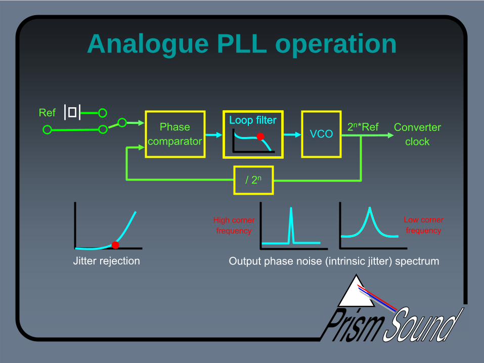
Analogue PLL operation
Phasecomparator
Loop filterLoop filterVCO
Ref
/ 2n
Converterclock
2n*Ref
Jitter rejection Output phase noise (intrinsic jitter) spectrum
High cornerfrequency
Low cornerfrequency

Some analogue PLL solutionsRef High fc RC
VCO
PLL Common, e.g. using DIR in DACPoor intrinsic jitter (RC multivibrator)Poor jitter rejection (high corner frequency)Good lock rangeLow cost
Ref Low fc QTZPLL
QTZ
Often found in better equipmentGood intrinsic jitter (hiQ
quartz VCXO)Good jitter rejection (low corner frequency)Possibly inadequate lock range (hiQ
qtz)High cost (two or more VCXOs)
Ref Low fc
PLL1
LGSVCO /n
PLL2
LCVCO
High fcGood overall analogue solutionGood intrinsic jitter (LF hiQ
and HF
loQ)Good jitter rejection (PLL1)Good lock range (LGS: lower Q than quartz)Moderate cost (only one VCXO)

Example of a hybrid PLL
From Cirrus CS2000
datasheet

Power supply issues•
Switching PSUs
have many advantages over linear:
Linear PSUs
are large, heavy, inefficient (hot) and expensiveSwitching PSUs
aren’t, but…
•
They are often feared by high-end audio designers who perceive them as:An unmanageable source of interference into the analogue
audio partsAn EMC approval headacheA reliability risk
•
Yet…They can be tamedIn DC-powered cases, they may be a necessity

Drawbacks of a basic SMPS
From ST application note AN1326
Flyback
converter is a popular choice…
Resonant SMPS topologies•
Wouldn’t it be nice if we had 500kHz
mains?
Resonant SMPS
approximates a sine wave through the transformer, by adding a resonant tank circuit in the primary, with zero-current/voltage switching
It’s more complex and expensive than the simple flyback
SMPS, and may be difficult to operate in off-line universal-input mode
But we only really need to achieve resonant operation at the switching points
•
Quasi-resonant SMPSA simple adaptation of a basic flyback
converter, which uses resonance at the switching points to reduce switching noise and losses
•
Difficulty in selecting appropriate SMPS
topology for audioManufacturers’
selection guides recommend simple topologies for low-power applications
But for audio, interference can be reduced by designinglow-power versions of higher-power topologies

Quasi-resonant SMPS
From NXP
TEA1507
application note

EMI improvement
From ST application note AN1326
Flyback
SMPS
conducted EMI Quasi-resonant SMPS
conducted EMI

Other SMPS considerations•
Cross-regulationCritical rails may benefit from linear post-regulation
•
Power-factor-correction (PFC) Reduces power-line distortion Can be useful in guaranteeing constant DC at SMPS
input for improved resonant and quasi-resonant performance
•
Beware recent efficiency legislation/guidelinesEU Ecodesign
Directive, US EnergyStar
Typically >80% efficiency for <20W unitsAnd <0.5W when units are in ‘standby’

Analogue signal path issues•
Opamp
stages (for that is what we shall use…)
Understand opamp
circuit noise modelsChoose the gain structure so as to maximize the signalChoose the right topologies, e.g. inverting stages usually cause
less distortion than non-invertingConsider a balanced signal path throughoutThink about bandwidthChoose the best opamp
‘on paper’
for each job –
then try some
othersRemember: there is no ‘best audio opamp’
•
Converter buffersΣ∆
ADC inputs often have non-linear characteristics and all
alias HF, requiring careful ADC buffer designCurrent output DACs
require careful
IVC
design

Analogue signal path issues•
Passive componentsResistor types: metal film or thin film (thick film ‘chip’
resistors
are nasty)Capacitor types: C0G/NP0
ceramic or low-loss plastic e.g.
polystyrene•
PhysicalGround planes, small SMT
components, laying down where
possibleTight channel strip layout, output/ground nodes outward, input
nodes inward, consider dual opamp
packagesConsider galvanic isolation between analogue and digital
domainsLots of test points, especially on the prototype

Look after the reference voltage…•
The reference voltage is very importantThe input to the converter is multiplied by its reference voltage (or
current) to produce the output, so the reference is just as critical as the analogue path
Reference care is your responsibility -
keep connections very shortPay attention to reference voltage decoupling capacitorsConsider driving reference voltage pins from a quiet, well-regulated
external source (not the power rail!)Pay attention to reference current IVC
resistors
•
A tip:If you have an elusive performance problem and the analogue signal
path looks fine: don’t forget the referenceIf it looks like modulation (sidebands or a noise skirt around the signal
frequency): if it gets worse with increasing signal frequency, it’s jitter; if it doesn’t, it’s probably a reference voltage problem
Digital path issues•
Digital processing (including ‘accidental’
processing)
Make sure that any bundled DSP
functions maintain sufficient precision not to let the analogue part down
Make sure that WLR schemes (dither, noise shaping etc.) pass on pre-WLR linearity below the WLR noise floor
For computer interfaces, remember the driver and the parts of the OS that you thought weren’t involved –
it’s vital to have
test gear to generate/analyze in the ‘computer domain’•
InterferenceModern converter sub-systems contain many hostile
asynchronous digital parts; despite lower voltages and smaller packages, modern chips have fast edge times which are hostile irrespective of operating frequency
Try to merge functionality into fewer devices,e.g. FPGAs
Observe good EMC design practices

System considerations•
Major decisions to make at the outset, although probably dictated by project requirements:Power source: DC-powered (wart or ‘computer bus’), or line-
powered (linear or SMPS
supply?)Habitat: own housing, or cohabiting with digital parts, or worse
in host computer? Do we need/can we afford screening cans?
Manufacturing technology: SMT
or THP, or mixed? Number of PCB layers available may affect plane topology
Isolation: can we galvanically
isolate analogue and digital grounds using optical or magnetic isolators?
EMC, efficiency: what statutory/voluntary directives will apply?

Assessment•
Measurement vs
listening
It’s better to debug and refine the design through objective measurement before subjective evaluation
•
EquipmentAn audio analyzer which can generate/analyze in the analogue and
digital domains (including the ‘computer domain’) is vitalAn RF
spectrum analyzer is useful for wideband inspection, especially
in SMPS
and computer-based designs; needed for EMC pre- compliance in any case
•
I like to…Set up the audio analyzer to be able to switch conveniently between
the important measurementsDisplay a high-resolution FFT
all the time –
it’s very handy when
tinkering

Summary of converter transparency parameters
Transparency Linearity Distortion THD
(vs
freq, ampl)
IMD
(close tone etc.)
Frequency response Amplitude response
Phase response
Nyquist Aliasing/imaging
Sampling jitter Intrinsic
Rejection
Quantisation Low-level linearity
Dither, noise-shaping action
Interference Modulation (RFI, powerline)
Additive Intrinsic noise In band
Out of band
Crosstalk Channel
Source etc.
Interference RFI
Powerline