performance analysis ofelectrical characteristics ofsingle ... · 1,2,3(department of physics,...
TRANSCRIPT

American Journal of Engineering Research (AJER) 2018
American Journal of Engineering Research (AJER)
e-ISSN: 2320-0847 p-ISSN : 2320-0936
Volume-7, Issue-6, pp-248-259
www.ajer.org Research Paper Open Access
w w w . a j e r . o r g
Page 248
Performance Analysis ofElectrical Characteristics ofSingle Gate
andDouble Gate Nano-MOSFET Devices
G.S.M Galadanci1, Abdulrazak Tijjani
2, SulaimanMuhammad Gana
3
[email protected], [email protected], [email protected]
1,2,3(Department of Physics, Bayero University, Kano, Nigeria)
Corresponding Author: G.S.M Galadanci
ABSTRACT:Metal oxide semiconductor field effect transistor (MOSFET) is a semiconductor device used in
many electronic devices for amplification and switching electrical signals. In modern era, low power portable
devices require more transistors to be integrated on a single chip to perform immeasurable number of functions
with high speed, low power consumption and less propagation delay since the number of circuits in a chip keeps
increasing daily. MOSFET downscaling has been the driving force towards the technological advancement, but
continuous scaling down of MOSFET causes problem of high power dissipation, high leakage current, Short
Channel Effects (SCEs), excessive process variation and reliability issues. In this work, performance analysis of
electrical characteristics of single gate and double gate nano-MOSFET devices are investigated using FETTOY
simulating software at room temperature (RT) by varying the oxide thickness from 0.3nm to 1.2nm to determine
the drain current, quantum capacitance, transconductance, quantum capacitance/insulator capacitance and
mobile electron. We can conclude that in deep nanometer regime, double gate MOSFET device have advantages
over single gate due to high conductivity to reduce leakage current and short channel effects (SCEs).
KEYWORDS -DG MOSFET, FETTOY, SG MOSFET, Short channel effects (SCEs)
----------------------------------------------------------------------------------------------------------------------------- ----------
I. INTRODUCTION
Silicon-based microelectronic devices have revolutionized our world in the past four decades. It all
started with the invention of integrated circuit in late 1950’s that unveiled the possibility of using transistors in
almost all kinds of electronic circuits. The breakthrough came with the demonstration of the first metal-oxide
semiconductor field-effect transistor (MOSFET) by Kahng and Atalla [1] which would enable cost effective
integration of large number of transistors with interconnections on a single silicon chip. Five years later, Gordon
Moore made the very important observation that the number of components on minimum cost integrated circuits
had increased roughly by a factor of two per year which then later transformed itself into a law known as the
Moore’s Law [2]. Moore’s Law is achieved primarily by scaling the transistor dimensions by a factor of 2 every
3 years. CMOS devices have been scaled down aggressively in each technology generations to achieve higher
integration density and performance [3]. As the device dimensions are getting smaller and smaller, scaling the
silicon based MOSFET devices for barrier potential, threshold voltage, oxide thickness, critical electric field etc.
are becoming increasingly harder. Further scaling down of MOSFET causes problem of high power dissipation,
high leakage current, Short Channel Effects (SCEs), excessive process variation and reliability issues. Many
solutions are proposed to overcome these limitations. Some of the solutions include modifications on the
existing structures and technologies with a hope of extending their scalability, while other solutions encompass
the use of new materials and technologies to replace the existing silicon MOSFETS [4]. Many works have been
done on transistor miniaturization, as transistor decreased in size, the thickness of the gate dielectric has steadily
been decreased to increase the gate capacitance and drive current, thereby improving reliability, raising device
performance and reducing power dissipation [5]. In this interesting journey of transistor size reduction, single
gate MOSFET is expected to exhibit a problem of short channel effects (SCE) which will lead to less scaling
capabilities [6]. Studies on the effects of gate length and oxide thickness on DG-MOSFET and concluded that
the short channel effect (SCEs) in DG-MOSFET is reduced and thinner gate oxide are necessary for higher drain

American Journal of Engineering Research (AJER) 2018
w w w . a j e r . o r g
Page 249
current [7]. Study the effect of gate length on the operation of silicon-on insulator (SOI) MOSFET structure,
using three transistors with gate lengths of 100, 200 and 500 nm with a fixed channel length of 500nm were
simulated and when the gate length is increased the output drain current characteristics slope and the transistor
transconductance increases [8]. The effect of gate length on DG-MOSFET at nano regime was studied, where
by DG-MOSFETs with gate lengths of 20,40, 60, 80 and 100nm were simulated respectively with a fixed
channel length of 100nm, oxide thickness of 1.0nm and channel thickness of 3nm, using simulation software
nanoFET [9]. A double gate (DG) MOSFET which comprises of conducting channel surrounded by gate
electrodes on either side offers distinct advantage for scaling and will have improved gate-channel control for
reduction of short-channel effects (SCEs) [6]. DG-MOSFET has higher drive current and transconductance,
lower leakage current thus better scaling capability when compared to the bulk MOSFET [10]. Gate oxide stack
with high-k materials in the oxide region was proposed by [11] to suppress the gate leakage current with
continuous thinning of gate oxide layer but this alternative is yet to demonstrate performance that is superior to
planar MOSFET [10, 11].
In this work, performance analysis of electrical characteristics of single gate and double gate nano-
MOSFET devices are investigated using FETTOY simulating software at room temperature (RT) by varying the
oxide thickness from 0.3nm to 1.2nm in accordance to international technology roadmap for semiconductors
(ITRS) [12], to overcome some limits and facilitate further scaling down of device dimensions by studying the
performance analysis of electrical characteristic of oxide thickness on drain current, quantum capacitance,
transconductance, quantum capacitance/insulator capacitance and mobile electron of single gate and double gate
nano MOSFET devices via simulation with nanoelectronics device simulation software FETTOY.
II. STRUCTURE OF SINGLE GATE AND DOUBLE GATE NANO-MOSFET
The traditional metal–oxide–semiconductor (MOS) structure is obtained by growing a layer of silicon
dioxide (SiO2) on top of a silicon substrate and depositing a layer of metal or polycrystalline silicon. As the
silicon dioxide is a dielectric material, its structure is equivalent to a planar capacitor, with one of the electrodes
replaced by a semiconductor. A MOSFET is based on the modulation of charge concentration by a MOS
capacitance between a body electrode and a gate electrode located above the body and insulated from all other
device regions by a gate dielectric layer which in the case of a MOSFET is an oxide, such as silicon dioxide as
shown in figure 1. In single gate MOSFET as the oxide thickness decreases the QC increases significantly as the
gate voltage increases [13].
Figure 1: Single Gate Nano-MOSFET
In double-gate MOSFET both gates control the current in the device as shown in Figure 2. Dual-gated
FETs are more immune to short channel effects and hence can be scaled to shorter dimensions than single gate
MOSFETs, for the same channel thickness. Also, dual-gated FETs have higher performance, due to lower
parasitic capacitance to ground. Like the single gate MOSFET, in double gate MOSFET also the QC increases
significantly with the decrease in gate oxide thickness [13].
Figure 2: Double Gate Nano-MOSFET
American Journal of Engineering Research (AJER) 2018
w w w . a j e r . o r g
Page 250
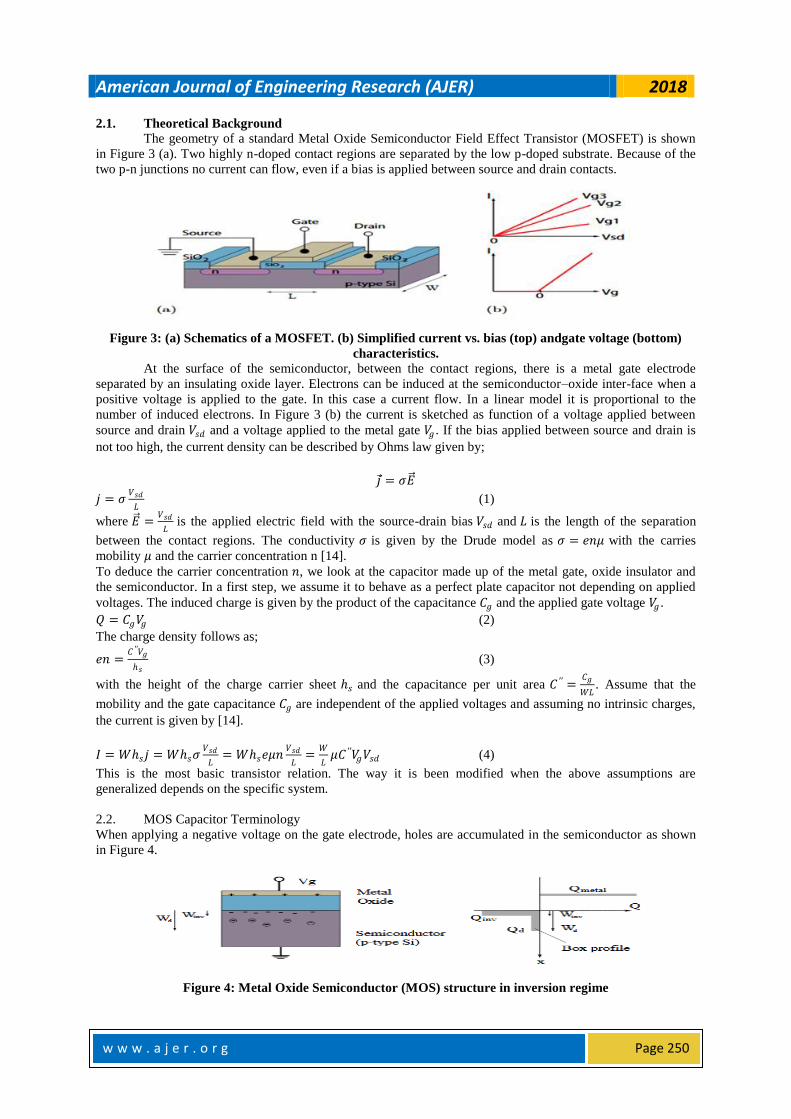
2.1. Theoretical Background
The geometry of a standard Metal Oxide Semiconductor Field Effect Transistor (MOSFET) is shown
in Figure 3 (a). Two highly n-doped contact regions are separated by the low p-doped substrate. Because of the
two p-n junctions no current can flow, even if a bias is applied between source and drain contacts.
Figure 3: (a) Schematics of a MOSFET. (b) Simplified current vs. bias (top) andgate voltage (bottom)
characteristics.
At the surface of the semiconductor, between the contact regions, there is a metal gate electrode
separated by an insulating oxide layer. Electrons can be induced at the semiconductor–oxide inter-face when a
positive voltage is applied to the gate. In this case a current flow. In a linear model it is proportional to the
number of induced electrons. In Figure 3 (b) the current is sketched as function of a voltage applied between
source and drain 𝑉𝑠𝑑 and a voltage applied to the metal gate 𝑉𝑔 . If the bias applied between source and drain is
not too high, the current density can be described by Ohms law given by;
𝑗 = 𝜎𝐸
𝑗 = 𝜎𝑉𝑠𝑑
𝐿 (1)
where 𝐸 =𝑉𝑠𝑑
𝐿 is the applied electric field with the source-drain bias 𝑉𝑠𝑑 and 𝐿 is the length of the separation
between the contact regions. The conductivity 𝜎 is given by the Drude model as 𝜎 = 𝑒𝑛𝜇 with the carries
mobility 𝜇 and the carrier concentration n [14].
To deduce the carrier concentration 𝑛, we look at the capacitor made up of the metal gate, oxide insulator and
the semiconductor. In a first step, we assume it to behave as a perfect plate capacitor not depending on applied
voltages. The induced charge is given by the product of the capacitance 𝐶𝑔 and the applied gate voltage 𝑉𝑔 .
𝑄 = 𝐶𝑔𝑉𝑔 (2)
The charge density follows as;
𝑒𝑛 =𝐶 ′′𝑉𝑔
𝑠 (3)
with the height of the charge carrier sheet 𝑠 and the capacitance per unit area 𝐶 ′′ =𝐶𝑔
𝑊𝐿. Assume that the
mobility and the gate capacitance 𝐶𝑔 are independent of the applied voltages and assuming no intrinsic charges,
the current is given by [14].
𝐼 = 𝑊𝑠𝑗 = 𝑊𝑠𝜎𝑉𝑠𝑑
𝐿= 𝑊𝑠𝑒𝜇𝑛
𝑉𝑠𝑑
𝐿=
𝑊
𝐿𝜇𝐶 ′′𝑉𝑔𝑉𝑠𝑑 (4)
This is the most basic transistor relation. The way it is been modified when the above assumptions are
generalized depends on the specific system.
2.2. MOS Capacitor Terminology
When applying a negative voltage on the gate electrode, holes are accumulated in the semiconductor as shown
in Figure 4.
Figure 4: Metal Oxide Semiconductor (MOS) structure in inversion regime

American Journal of Engineering Research (AJER) 2018
w w w . a j e r . o r g
Page 251
These holes are at the interface to the oxide within a thin layer called accumulation layer. When a
positive voltage is applied, the intrinsic holes must be depleted. In the depletion region, there are no mobile
charges, but only the immobile acceptor ions. The depletion approximation is used with assumption that the
depleted charge 𝑄𝑑 has a box profile of width 𝑊𝑑 . Thus,
𝑄𝑑 = −𝑒𝑁𝑎𝑊𝑑 (5)
where;
𝑁𝑎 is the acceptor dopant density.
𝑒 is the elementary charge.
When the gate voltage is driven further, electrons are induced at the interface and build up the inversion charge
𝑄𝑖𝑛𝑣 in the thin inversion layer of width 𝑊𝑖𝑛𝑣 . The transfer from accumulation to depletion region
occurs at finite voltage 𝑉𝑓𝑏 called flat band voltage. It is the voltage at which the bands in the semiconductor are
flat all the way from the bulk to the oxide interfaces.
In real devices one needs to consider charges within the oxide 𝑄𝑜𝑥 .They contribute via the gate capacitance 𝐶𝑔
so that the total flat band voltage is given by;
𝑉𝑓𝑏 = 𝜙𝑚 − 𝜙𝑠 −𝑄𝑜𝑥
𝐶𝑔 (6)
where;
𝜙𝑚 is the work function of the metal
𝜙𝑠 is the work function of the silicon
In the depletion region all acceptors are ionized, and the potential is described by the Poisson equation [15];
Ψ =𝑒𝑁𝑎
2𝜀𝑟𝜀𝑜(𝑥 − 𝑊𝑑 )2 (7)
The potential at the interface is given by the surface potential Ψ 0 = Ψ𝑠 , thus, the depletion width is given by
[15];
𝑊𝑑 = 2𝜀𝑟𝜀𝑜Ψ𝑠
𝑒𝑁𝑎 (8)
2.3. MOS Capacity
In MOS capacitor the voltage applied on the gate partially drops across the insulator and partly within the
semiconductor given by [15];
𝑉𝑔 = 𝑉𝑖 + 𝑉𝑠 (9)
where;
𝑉𝑠is the voltage drop within the semiconductor corresponds to the surface potential Ψ𝑠
𝑉𝑖 is the voltage drop across the insulator given by the charge 𝑄𝑠 on the semiconductor [15];
𝑉𝑖 = 𝐸 𝑑 =𝑄𝑠
𝐴𝑑
𝜀𝑆𝑖 02𝜀𝑜=
𝑄𝑠
𝐶𝑜𝑥 (10)
With the oxide capacitor 𝐶𝑜𝑥 = 𝐴𝜀𝑆𝑖02𝜀𝑜/𝑑 where d is the thickness of the oxide and A the area of the interface.
The relation between the applied gate voltage and the surface potential is given by [15];
𝑉𝑔 =𝑄𝑠
𝐶𝑜𝑥+ Ψ𝑠 (11)
In depletion regime, the plates capacitor separated by the depletion width 𝑊𝑑 is given by [15];
𝐶𝑑 =𝜀𝑆𝑖 𝜀𝑜
𝑊𝑑 (12)
The total gate capacitance is the series capacitance of the oxide capacitance and the depletion capacitance given
by [16];
1
𝐶𝑔 = 1
𝐶𝑜𝑥 + 1
𝐶𝑑 (13)
In accumulation and strong inversion, the depletion width goes to zero and the total gate capacitance 𝐶𝑔 is
dominated by 𝐶𝑜𝑥 .

American Journal of Engineering Research (AJER) 2018
w w w . a j e r . o r g
Page 252
2.4. Subthreshold Regime
In depletion, the small mobile charge that can be thermally excited in the depletion zone gives rise to a small
subthreshold current. The carrier concentration is far away from the Fermi energy is given by the Boltzmann
distribution 𝑛 = 𝑛𝑖exp(−𝑒Ψ𝑘𝑇 ) and so.
𝑄 = 𝑒 𝑛 𝑥 𝑑𝑥 = 𝑒 𝑛(Ψ)
𝑑Ψ/dx𝑑Ψ = e𝑛𝑖
1
𝑑Ψ/dxexp(−𝑒Ψ
𝑘𝑇 )𝑑Ψ0
Ψ𝑠
0
Ψ𝑠
𝑊𝑑
0 (14)
The integral approximatively is given by [17];
𝑄 = 𝐾𝑇 𝜀𝑆𝑖 𝜀𝑜
2𝑒Ψ𝑠𝑁𝑎
𝑛𝑖
𝑁𝑎
2
exp −𝑒Ψ𝑘𝑇 (15)
The mobile charge in the depletion region and the current in the subthreshold regime depend exponentially on
the surface potential Ψ𝑠: 𝐼 ∝ exp −𝑒Ψ𝑘𝑇 .
The subthreshold swing S is defined as the gate voltage charge needed to suppress the subthreshold current [17].
𝑆 = 𝑑𝑉𝑔
𝑑(log 𝐼 ) = 𝐼𝑛 10
𝑑𝑉𝑔
𝑑 In 𝐼 = 𝐼𝑛(10)
𝑑𝑉𝑔
𝑒/𝑘𝑇𝑑 Ψ𝑠 (16)
𝑆 = 59.6𝑚𝑉𝑘𝑇
𝑒 1 +
𝐶𝑑
𝐶0𝑥 (17)
III. MATETRIALS AND SIMULATION METHOD
This section will discuss the materials that are used, simulating tools and method of simulation.
3.1. Materials
The materials that are used in this research are silicon dioxide as the gate dielectric, silicon substrate as base
material and FETTOY as simulating tools available on nanohub.org.
Nanohub.org is the premier place for computational nanotechnology research, education, and collaboration. This
site hosts a rapidly growing collection of simulation tools for nanoscale phenomena that run in the cloud and are
accessible through a web browser. In addition to simulations, nanoHUB provides online presentations, cutting-
edge nanoHUB-U short courses, animations, teaching materials, and more. These resources help users learn
about simulation tools and about nanotechnology in general.
3.2. Method of Simulation
FETTOY tool is a numerical simulator that calculate the ballistic I-V characteristics for a conventional single
gate MOSFET and double gate MOSFET. For conventional MOSFET, FETTOY assumes either single or
double gate geometry.
Figure 5: FETTOY Software interface
The simulating procedure was as follows;
1. Modelling of the device was done by choosing the device type (Single gate and Double gate nano-
MOSFET).
2. Setting the oxide thickness from 0.3 to 1.2nm, Gate voltage and Drain voltage 0-1V with other parameters
fixed as shown in table 1.
American Journal of Engineering Research (AJER) 2018
w w w . a j e r . o r g
Page 253
Table 1: Values of Input Parameters FETTOY
INPUT PARAMETERS
VALUES
Oxide Thickness 0.3-1.2(nm)
Insulator dielectric constant 3.9
Temperature 300 (K)
Initial gate voltage 0 (V)
Final gate voltage 1 (V)
Number of bias points (gate) 13
Initial drain voltage 0 (V)
Final drain voltage 1 (V)
Number of bias points (drain) 13
threshold voltage 0.32
Gate control parameter 0.88
Drain control parameter 0.035
Series Resistance 0 (ohms)
Doping Density 1e+26 (/m^3)
Si Body Thickness 1e-08 (m)
Transport Effective Mass 0.19
Valley Degeneracy 2
3. The program is then run to obtain results for each set of devices chosen.
4. Drain current, quantum capacitance, transconductance, quantum capacitance/insulator capacitance and
mobile electron were obtained, and the results was analyzed for all the devices.
IV. RESULTS AND DISCUSSION
This section illustrates the simulation studies that have been carried out using nanoHUB tools [18]. Table 2 and
Table 3 shows the simulation results of single gate and double gate nano-MOSFET respectively for input
parameter given in Table 1, in determining the drain current at different gate voltage, oxide thickness and at a
constant drain voltage of 1V.
Table 2: Drain current against Gate Voltage at different Oxide Thickness in Single Gate MOSFET
Table 3: Drain current against Gate Voltage at different Oxide Thickness in Double Gate MOSFET
Single Gate MOSFET
At drain voltage 1V
Gate
Voltage
(V)
Drain current (uA/um)
𝑇𝑜𝑥 = 0.3𝑛𝑚 𝑇𝑜𝑥 = 0.5𝑛𝑚 𝑇𝑜𝑥 = 0.7𝑛𝑚 𝑇𝑜𝑥 = 0.9𝑛𝑚 𝑇𝑜𝑥 = 1.2𝑛𝑚
0 6.72e-03 6.72e-03 6.72e-03 6.72e-03 6.72e-03
0.083333 1.14e-01 1.14e-01 1.14e-01 1.14e-01 1.14e-01
0.166666 1.94e+00 1.93e+00 1.92e+00 1.92e+00 1.91e+00
0.25 30.1 28.9 27.8 26.8 25.5
0.333333 257 213 183 162 140
0.416666 875 647 517 433 351
0.5 1830 1280 988 803 628
0.583333 3070 2090 1570 1250 960
0.666666 4570 3050 2250 1770 1340
0.75 6260 4150 3030 2360 1760
0.833333 8110 5360 3900 3020 2220
0.916666 10100 6680 4850 3740 2730
1 12300 8090 5860 4510 3290
Double Gate MOSFET
At drain voltage 1V
Gate
Voltage (V)
Drain current (uA/um)
𝑇𝑜𝑥 = 0.3𝑛𝑚 𝑇𝑜𝑥 = 0.5𝑛𝑚 𝑇𝑜𝑥 = 0.7𝑛𝑚 𝑇𝑜𝑥 = 0.9𝑛𝑚 𝑇𝑜𝑥 = 1.2𝑛𝑚
0 6.72e-03 6.72e-03 6.72e-03 6.72e-03 6.72e-03
0.083333 1.14e-01 1.14e-01 1.14e-01 1.14e-01 1.14e-01
0.166666 1.94e+00 1.94e+00 1.93e+00 1.93e+00 1.93e+00
0.25 31.1 30.4 29.8 29.2 28.3
0.333333 309 272 244 222 197
0.416666 1200 962 803 692 575
0.5 2670 2050 1660 1390 1120
0.583333 4600 3470 2750 2270 1790

American Journal of Engineering Research (AJER) 2018
w w w . a j e r . o r g
Page 254
It has been observed from Table 2 and Table 3 that the drain current of double gate nano-MOSFET
increases with the reduction in oxide thickness. It means that when reducing the oxide thickness, the current
capability of double gate nano-MOSFET enhances. It is also observed from the simulation that at a very low
gate voltage such as 0V and 0.083V, the value of drain current is the same for all oxide thickness considered. A
graph of drain current against gate voltage was plotted for both single gate and double gate nano-MOSFET for
all oxide thickness (0.3nm, 0.5nm, 0.7nm, 0.9nm and 1.2nm) as shown in Fig.6 and Fig.7, we can conclude that
the conductivity of the double gate nano-MOSFET is inversely proportional to the oxide thickness.
Table 4 and Table 5 shows the simulation results of single gate and double gate nano-MOSFET respectively for
input parameter given in Table 1, in determining the quantum capacitance at different gate voltage, oxide
thickness and at a constant drain voltage of 1V.
Table 4: Quantum capacitance against Gate Voltage at different Oxide Thickness in Single Gate
MOSFET
0.666666 6890 5170 4080 3330 2590
0.75 9460 7090 5580 4550 3510
0.833333 12300 9200 7230 5890 4530
0.916666 15400 11500 9010 7330 5640
1 18700 13900 10900 8880 6830
Single Gate MOSFET
At drain voltage 1V
Gate Voltage
(V)
Quantum Capacitance (F/cm2)
𝑇𝑜𝑥 = 0.3𝑛𝑚 𝑇𝑜𝑥 = 0.5𝑛𝑚 𝑇𝑜𝑥 = 0.7𝑛𝑚 𝑇𝑜𝑥 = 0.9𝑛𝑚 𝑇𝑜𝑥 = 1.2𝑛𝑚
0 2.10e-10 2.10e-10 2.10e-10 2.10e-10 2.10e-10
0.083333 3.58e-09 3.58e-09 3.58e-09 3.58e-09 3.57e-09
0.166666 6.03e-08 6.02e-08 6.00e-08 5.98e-08 5.95e-08
0.25 8.97E-07 8.62E-07 8.31E-07 8.03E-07 7.65E-07
0.333333 5.62E-06 4.92E-06 4.41E-06 4.01E-06 3.56E-06
0.416666 1.04E-05 9.36E-06 8.47E-06 7.74E-06 6.86E-06
0.5 1.22E-05 1.15E-05 1.08E-05 1.02E-05 9.25E-06
0.583333 1.26E-05 1.23E-05 1.19E-05 1.15E-05 1.07E-05
0.666666 1.27E-05 1.26E-05 1.24E-05 1.21E-05 1.16E-05
0.75 1.28E-05 1.27E-05 1.26E-05 1.25E-05 1.21E-05
0.833333 1.28E-05 1.28E-05 1.27E-05 1.26E-05 1.24E-05
0.916666 1.28E-05 1.28E-05 1.28E-05 1.27E-05 1.26E-05

American Journal of Engineering Research (AJER) 2018
w w w . a j e r . o r g
Page 255
Table 5: Quantum capacitance against Gate Voltage at different Oxide Thicknessin Double Gate
MOSFET
It has been observed from Table 4 and Table 5 that the quantum capacitance (QC) of both single gate
and double gate nano-MOSFET increases significantly as the oxide thickness goes down from 1.2nm to 0.3nm,
and gate voltage increases. It is also observed from the simulation that at a very low gate voltage such as 0V and
0.083V, the value of quantum capacitance is the same for all oxide thickness considered here. A graph of
quantum capacitance against gate voltage was plotted for both single gate and double gate nano-MOSFET for
all oxide thickness (0.3nm, 0.5nm, 0.7nm, 0.9nm and 1.2nm) as shown in Fig.8 and Fig.9. For single gate
MOSFET, we can easily conclude that with decrease in oxide thickness the quantum capacitance increases at
different gate voltages. Whereas, in the case of double gate MOSFET under identical simulating condition the
decrease in gate oxide thickness the quantum capacitance increases at different gate voltages. However, it
saturated above 0.75 V for very small oxide thickness such as 0.3nm, 0.5nm, 0.7nm and 0.9nm.
Table 6 and Table 7 shows the simulation results of single gate and double gate nano-MOSFET respectively for
input parameter given in Table 1, in determining the Gm/Id at different gate voltage, oxide thickness and at a
constant drain voltage of 1V.
Table 6: Gm/Id against Gate Voltage at different Oxide Thickness in Single Gate MOSFET
1 1.28E-05 1.28E-05 1.28E-05 1.27E-05 1.27E-05
Double Gate MOSFET
At drain voltage 1V
Gate Voltage
(V)
Quantum Capacitance (F/cm2)
𝑇𝑜𝑥 = 0.3𝑛𝑚 𝑇𝑜𝑥 = 0.5𝑛𝑚 𝑇𝑜𝑥 = 0.7𝑛𝑚 𝑇𝑜𝑥 = 0.9𝑛𝑚 𝑇𝑜𝑥 = 1.2𝑛𝑚
0 2.10e-10 2.10e-10 2.10e-10 2.10e-10 2.10e-10
0.083333 3.58e-09 3.58e-09 3.58e-09 3.58e-09 3.58e-09
0.166666 6.05e-08 6.04e-08 6.03e-08 6.02e-08 6.01e-08
0.25 9.27E-07 9.07E-07 8.88E-07 8.71E-07 8.46E-07
0.333333 6.35E-06 5.83E-06 5.42E-06 5.07E-06 4.64E-06
0.416666 1.14E-05 1.07E-05 1.02E-05 9.61E-06 8.89E-06
0.5 1.26E-05 1.23E-05 0.000012 1.17E-05 1.12E-05
0.583333 1.27E-05 1.27E-05 1.26E-05 1.24E-05 1.21E-05
0.666666 1.28E-05 1.28E-05 1.27E-05 1.27E-05 1.25E-05
0.75 1.28E-05 1.28E-05 1.28E-05 1.27E-05 1.27E-05
0.833333 1.28E-05 1.28E-05 1.28E-05 1.28E-05 1.27E-05
0.916666 1.28E-05 1.28E-05 1.28E-05 1.28E-05 1.28E-05
1 1.28E-05 1.28E-05 1.28E-05 1.28E-05 1.28E-05
Single Gate MOSFET
At drain voltage 1V
Gate Gm/id

American Journal of Engineering Research (AJER) 2018
w w w . a j e r . o r g
Page 256
Table 7: Gm/Id against Gate Voltage at different Oxide Thickness in Double Gate MOSFET
It has been observed from Table 6 and Table 7 that the Gm/Id ratio of both single gate and double gate
nano-MOSFET increases significantly as the oxide thickness goes down from 1.2nm to 0.3nm, and gate voltage
increases this is due to the reason that gate oxide capacitance is increased as the gate insulator thickness is
reduced. It is also observed from the simulation that at a very low gate voltage such as 0V and 0.083V, the value
of Gm/Id ratio is the same for all oxide thickness considered. A graph of Gm/Id ratio against gate voltage was
plotted for both single gate and double gate nano-MOSFET for all oxide thickness (0.3nm, 0.5nm, 0.7nm, 0.9nm
and 1.2nm) as shown in Fig.10 and Fig.11.
Voltage (V)
𝑇𝑜𝑥 = 0.3𝑛𝑚 𝑇𝑜𝑥 = 0.5𝑛𝑚 𝑇𝑜𝑥 = 0.7𝑛𝑚 𝑇𝑜𝑥 = 0.9𝑛𝑚 𝑇𝑜𝑥 = 1.2𝑛𝑚
0 3.40e+01 3.40e+01 3.40e+01 3.40e+01 3.40e+01
0.083333 3.40e+01 3.40e+01 3.39e+01 3.39e+01 3.39e+01
0.166666 3.34e+01 3.32e+01 3.30e+01 3.28e+01 3.25e+01
0.25 29.3 28.2 27.3 26.6 25.7
0.333333 20.2 18.7 17.5 16.7 15.7
0.416666 11.8 10.8 10.1 9.59 9.03
0.5 7.54 7.02 6.65 6.37 6.05
0.583333 5.49 5.18 4.93 4.74 4.54
0.666666 4.26 4.12 3.95 3.8 3.63
0.75 3.44 3.4 3.31 3.2 3.05
0.833333 2.89 2.86 2.82 2.76 2.65
0.916666 2.49 2.46 2.45 2.42 2.34
1 2.32 2.3 2.28 2.26 2.21
Double Gate MOSFET
At drain voltage 1V
Gate
Voltage
(V)
Gm/id
𝑇𝑜𝑥 = 0.3𝑛𝑚 𝑇𝑜𝑥 = 0.5𝑛𝑚 𝑇𝑜𝑥 = 0.7𝑛𝑚 𝑇𝑜𝑥 = 0.9𝑛𝑚 𝑇𝑜𝑥 = 1.2𝑛𝑚
0 3.40e+01 3.40e+01 3.40e+01 3.40e+01 3.40e+01
0.083333 3.40e+01 3.40e+01 3.40e+01 3.40e+01 3.40e+01
0.166666 3.36e+01 3.35e+01 3.34e+01 3.33e+01 3.31e+01
0.25 30.4 29.7 29 28.5 27.8
0.333333 21.9 20.7 19.8 19 18.1
0.416666 12.9 12.1 11.5 11 10.4
0.5 8.06 7.7 7.39 7.13 6.82
0.583333 5.7 5.56 5.41 5.25 5.04
0.666666 4.32 4.29 4.24 4.17 4.04
0.75 3.48 3.45 3.44 3.41 3.36
0.833333 2.92 2.9 2.88 2.87 2.85
0.916666 2.52 2.5 2.48 2.47 2.46
1 2.35 2.33 2.31 2.3 2.29

American Journal of Engineering Research (AJER) 2018
w w w . a j e r . o r g
Page 257
Table 8 and Table 9 shows the simulation results of single gate and double gate nano-MOSFET respectively for
input parameter given in Table 1, in determining the QC/Insulator capacitance ratio at different gate voltage,
oxide thickness and at a constant drain voltage of 1V.
Table 8: QC/ Insulator Capacitance against Gate Voltage at different Oxide Thickness in Single Gate
MOSFET
Table 9: QC/ Insulator Capacitance against Gate Voltage at different Oxide Thickness in Double Gate
MOSFET
It has been observed from Table 8 and Table 9 that the QC/Insulator capacitance ratio of both single
gate and double gate nano-MOSFET decreases as the oxide thickness goes down from 1.2nm to 0.3nm, and gate
voltage increases. Lower drain voltage shows significant capacitance effect. It is also observed from the
simulation that at a very low gate voltage such as 0V and 0.083V, the value of QC/Insulator capacitance ratio is
the same for all oxide thickness considered.
Single Gate MOSFET
At drain voltage 1V
Gate
Voltage
(V)
Quantum Capacitance/Insulator Capacitance
𝑇𝑜𝑥 = 0.3𝑛𝑚 𝑇𝑜𝑥 = 0.5𝑛𝑚 𝑇𝑜𝑥 = 0.7𝑛𝑚 𝑇𝑜𝑥 = 0.9𝑛𝑚 𝑇𝑜𝑥 = 1.2𝑛𝑚
0 1.83e-05 3.05e-05 4.27e-05 5.49e-05 7.31e-05
0.083333 3.11e-04 5.18e-04 7.25e-04 9.32e-04 1.24e-03
0.166666 5.24e-03 8.71e-03 1.22e-02 1.56e-02 2.07e-02
0.25 0.078 0.125 0.169 0.209 0.266
0.333333 0.488 0.712 0.894 1.05 1.24
0.416666 0.907 1.36 1.72 2.02 2.38
0.5 1.06 1.67 2.19 2.65 3.22
0.583333 1.1 1.79 2.42 2.99 3.73
0.666666 1.11 1.83 2.52 3.16 4.04
0.75 1.11 1.84 2.56 3.25 4.21
0.833333 1.11 1.85 2.58 3.29 4.31
0.916666 1.11 1.85 2.59 3.31 4.37
1 1.11 1.85 2.59 3.32 4.4
Double Gate MOSFET
At drain voltage 1V
Gate
Voltage
(V)
Quantum Capacitance/Insulator Capacitance
𝑇𝑜𝑥 = 0.3𝑛𝑚 𝑇𝑜𝑥 = 0.5𝑛𝑚 𝑇𝑜𝑥 = 0.7𝑛𝑚 𝑇𝑜𝑥 = 0.9𝑛𝑚 𝑇𝑜𝑥 = 1.2𝑛𝑚
0 1.83e-05 3.05e-05 4.27e-05 5.49e-05 7.31e-05
0.083333 3.11e-04 5.18e-04 7.26e-04 9.33e-04 1.24e-03
0.166666 5.26e-03 8.75e-03 1.22e-02 1.57e-02 2.09e-02
0.25 0.0805 0.131 0.18 0.227 0.294
0.333333 0.552 0.845 1.1 1.32 1.61
0.416666 0.988 1.56 2.06 2.51 3.09
0.5 1.09 1.78 2.44 3.05 3.88
0.583333 1.11 1.84 2.55 3.24 4.22
0.666666 1.11 1.85 2.58 3.3 4.36
0.75 1.11 1.85 2.59 3.32 4.41
0.833333 1.11 1.85 2.59 3.33 4.43
0.916666 1.11 1.85 2.59 3.33 4.44
1 1.11 1.85 2.59 3.33 4.44
American Journal of Engineering Research (AJER) 2018
w w w . a j e r . o r g
Page 258
A graph of QC/Insulator capacitance ratio against gate voltage was plotted for both single gate and double gate
nano-MOSFET for all oxide thickness (0.3nm, 0.5nm, 0.7nm, 0.9nm and 1.2nm) as shown in Figure 12 and
figure 13.
Table 10 and Table 11 shows the simulation results of single gate and double gate nano-MOSFET respectively
for input parameter given in Table 1, in determining the mobile electron at different gate voltage, oxide
thickness and at a constant drain voltage of 1V.
Table 10: Mobile Electron against Gate Voltage at different Oxide Thickness inSingle Gate MOSFET
Table 11: Mobile Electron against Gate Voltage at different Oxide Thickness in Double Gate MOSFET
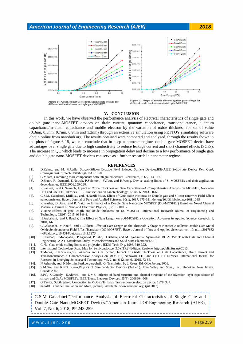
It has been observed from Table 10 and Table 11 that the mobile electron of both single gate and
double gate nano-MOSFET increases as the oxide thickness goes decreases from 1.2nm to 0.3nm, and gate
voltage increases. This shows that electrons in double move higher as the oxide thickness decreases. It is also
observed from the simulation that at a very low gate voltage such as 0V and 0.083V, the value of mobile
electron is the same for all oxide thickness considered.
A graph of mobile electron against gate voltage was plotted for both single gate and double gate nano-MOSFET
for all oxide thickness (0.3nm, 0.5nm, 0.7nm, 0.9nm and 1.2nm) as shown in Fig.14 and Fig.15.
Single Gate MOSFET
At drain voltage 1V
Gate Voltage
(V)
Mobile Electron (coul/mum)
𝑇𝑜𝑥 = 0.3𝑛𝑚 𝑇𝑜𝑥 = 0.5𝑛𝑚 𝑇𝑜𝑥 = 0.7𝑛𝑚 𝑇𝑜𝑥 = 0.9𝑛𝑚 𝑇𝑜𝑥 = 1.2𝑛𝑚
0 3.40e+07 3.40e+07 3.40e+07 3.40e+07 3.40e+07
0.083333 5.79e+08 5.79e+08 5.78e+08 5.78e+08 5.78e+08
0.166666 9.78e+09 9.75e+09 9.72e+09 9.69e+09 9.65e+09
0.25 1.5E+11 1.44E+11 1.39E+11 1.34E+11 1.28E+11
0.333333 1.2E+12 1E+12 8.74E+11 7.78E+11 6.74E+11
0.416666 3.51E+12 2.73E+12 2.25E+12 1.92E+12 1.59E+12
0.5 6.31E+12 4.79E+12 3.88E+12 3.27E+12 2.66E+12
0.583333 9.23E+12 6.96E+12 5.6E+12 4.69E+12 3.79E+12
0.666666 1.22E+13 9.17E+12 7.36E+12 6.15E+12 4.95E+12
0.75 1.51E+13 1.14E+13 9.14E+12 7.63E+12 6.12E+12
0.833333 1.81E+13 1.36E+13 1.09E+13 9.11E+12 7.31E+12
0.916666 2.11E+13 1.58E+13 1.27E+13 1.06E+13 8.49E+12
1 2.4E+13 1.81E+13 1.45E+13 1.21E+13 9.68E+12
Double Gate MOSFET
At drain voltage 1V
Gate Voltage
(V)
Mobile Electron (coul/mum)
𝑇𝑜𝑥 = 0.3𝑛𝑚 𝑇𝑜𝑥 = 0.5𝑛𝑚 𝑇𝑜𝑥 = 0.7𝑛𝑚 𝑇𝑜𝑥 = 0.9𝑛𝑚 𝑇𝑜𝑥 = 1.2𝑛𝑚
0 3.40e+07 3.40e+07 3.40e+07 3.40e+07 3.40e+07
0.083333 5.79e+08 5.79e+08 5.79e+08 5.79e+08 5.78e+08
0.166666 9.80e+09 9.79e+09 9.77e+09 9.76e+09 9.74e+09
0.25 1.56E+11 1.52E+11 1.49E+11 1.46E+11 1.42E+11
0.333333 1.42E+12 1.26E+12 1.14E+12 1.04E+12 9.33E+11
0.416666 4.54E+12 3.79E+12 3.27E+12 2.88E+12 2.46E+12
0.5 8.34E+12 6.86E+12 5.84E+12 5.09E+12 4.28E+12
0.583333 1.23E+13 1.01E+13 8.54E+12 7.42E+12 6.21E+12
0.666666 1.62E+13 1.33E+13 1.13E+13 9.78E+12 8.17E+12
0.75 2.01E+13 1.65E+13 1.4E+13 1.21E+13 1.01E+13
0.833333 2.41E+13 1.97E+13 1.67E+13 1.45E+13 1.21E+13
0.916666 2.8E+13 2.3E+13 1.95E+13 1.69E+13 1.41E+13
1 3.19E+13 2.62E+13 2.22E+13 1.93E+13 1.61E+13
American Journal of Engineering Research (AJER) 2018
w w w . a j e r . o r g
Page 259
V. CONCLUSION
In this work, we have observed the performance analysis of electrical characteristics of single gate and
double gate nano-MOSFET devices on drain current, quantum capacitance, transconductance, quantum
capacitance/insulator capacitance and mobile electron by the variation of oxide thickness for set of value
(0.3nm, 0.5nm, 0.7nm, 0.9nm and 1.2nm) through an extensive simulation using FETTOY simulating software
obtain online from nanohub.org. The results obtained were compared and analyzed, through the results shown in
the plots of figure 6-15, we can conclude that in deep nanometer regime, double gate MOSFET device have
advantages over single gate due to high conductivity to reduce leakage current and short channel effects (SCEs).
The increase in QC which leads to increase in propagation delay and decline to a low performance of single gate
and double gate nano-MOSFET devices can serve as a further research in nanometer regime.
REFERENCES [1]. D.Kahng, and M. MAtalla, Silicon-Silicon Dioxide Field Induced Surface Devices.IRE-AIEE Solid-state Device Res. ConJ,
(Carnegie Inst. of Tech., Pittsburgh, PA), 1960.
[2]. G.Moore, Cramming more components onto integrated circuits. Electronics, 1965, 114-117. [3]. D.Frank, R. Dennard, E.Nowak, P.Solomon, Y.Taur, and H.Wong, Device scaling limits of Si MOSFETs and their application
dependencies. IEEE,2001,259-288.
[4]. K.Sanjeet, and C.Suarabh, Impact of Oxide Thickness on Gate Capacitance-A Comprehensive Analysis on MOSFET, Nanowire
FET and CNTFET DEvices. IEEE transactions on nanotechnology, 12, no. 6.,2013, 50-62.
[5]. G.S.M. Galadanci, I.Bilkisu, and, H.Nazifi Musa, Effect of Gate oxide thickness on Double gate and Silicon nanowire Field Effect
nanotransistors. Bayero Journal of Pure and Applied Sciences, 10(1), 2017, 675-681. doi.org/10.4314/bajopas.v10i1.126S [6]. R.Prasher, D.Dass, and R. Vaid, Performance of a Double Gate Nanoscale MOSFET (DG-MOSFET) Based on Novel Channel
Materials. Journal of Nano and Electronic Physics, 5, 2013, 01017.
[7]. V.Harsh,Effects of gate length and oxide thickness on DG-MOSFET. International Research Journal of Engineering and Technology, 02(08), 2015, 938-941.
[8]. H.Arabshahi, and J. Baedia, The Effect of Gate Length on SOI-MOSFETs Operation. Advances in Applied Science Research, 1,
2010, 14-18. [9]. G.Galadanci, M.Nazifi, and I. Bilikisu, Effect of Gate Length on the Threshold Voltage of Nanoscale Ballistic Double Gate Metal
Oxide Semiconductor Field Effect Transistor (DG-MOSFET). Bayero Journal of Pure and Applied Sciences, vol. 10, no.1.,2017682
- 688.doi.org/10.4314/bajopas.v10i1.127S [10]. K.Pradhan, S.Mohapatra, P.Agarwal, P.Sahu, D.Behera, and M. Jyotismita, Symmetric DG-MOSFET with Gate and Channel
Engineering. A 2-D Simulation Study, Microelectronics and Solid State Electronics2013.
[11]. C.Hu, Gate oxide scaling limits and projection. IEDM Tech. Dig, 1996, 319-322. [12]. International Technology Road Map for Semiconductors 2.0 (ITRS),Edition. Retrieve: http://public.itrs.net/2015.
[13]. T.Manas, K.K.Sharma,S.R.Lokendra and C.K. Vinod, Impact of Oxide Thickness on Gate Capacitance, Drain current and
Transconductance-A Comprehensive Analysis on MOSFET, Nanowire FET and CNTFET DEvices. International Journal for Research in Emerging Science and Technology, vol. 2, no. 6 12, no. 6., 2015, 73-85.
[14]. N.Ashcroft, and, N.Mermin,Festkoerperpyhsik, G. Translation by J. Gress, Ed. Oldenbourg, 2001.
[15]. S.M.Sze, and K.NG. Kwok,Physics of Semiconductor Devices (3rd ed.). John Wiley and Sons., Inc., Hoboken, New Jersey,
Canada.2007.
[16]. S.Pal, K.Cantely, S.Ahmed, and L.MS, Inflence of band structure and channel structure of the inversion layer capacitance of
silicon and GaAs MOSFETs. IEEE Trans. Electron. Devices, 55(3), 2008904-908. [17]. G.Taylor, Subthreshold Conduction in MOSFETs. IEEE Transaction on electron device, 1978, 337.
[18]. nanoHUB online Simulation and More, [online]. Available: www.nanohub.org. (jul.2012).
G.S.M Galadanci."Performance Analysis of Electrical Characteristics of Single Gate and
Double Gate Nano-MOSFET Devices.”American Journal Of Engineering Research (AJER),
Vol. 7, No. 6, 2018, PP.248-259.