steady-state and transient electron transport...
TRANSCRIPT

J Mater Sci: Mater Electron (2006) 17: 87–126
DOI 10.1007/s10854-006-5624-2
R E V I E W
Steady-State and Transient Electron Transport Within the III–VNitride Semiconductors, GaN, AlN, and InN: A ReviewStephen K. O’Leary∗ · Brian E. Foutz† ·Michael S. Shur · Lester F. Eastman
Received: 15 July 2005 / Accepted: 26 July 2005C© Springer Science + Business Media, Inc. 2006
Abstract The III–V nitride semiconductors, gallium nitride,
aluminum nitride, and indium nitride, have, for some time
now, been recognized as promising materials for novel elec-
tronic and optoelectronic device applications. As informed
device design requires a firm grasp of the material properties
of the underlying electronic materials, the electron transport
that occurs within these III–V nitride semiconductors has
been the focus of considerable study over the years. In an
effort to provide some perspective on this rapidly evolving
field, in this paper we review analyses of the electron trans-
port within the III–V nitride semiconductors, gallium nitride,
aluminum nitride, and indium nitride. In particular, we dis-
cuss the evolution of the field, compare and contrast results
determined by different researchers, and survey the current
literature. In order to narrow the scope of this review, we will
primarily focus on the electron transport within bulk wurtzite
gallium nitride, aluminum nitride, and indium nitride, for this
analysis. Most of our discussion will focus on results ob-
tained from our ensemble semi-classical three-valley Monte
∗Author to whom correspondence should be addressed.
†Present address: Cadence Design Systems, 6210 Old Dobbin Lane,Columbia, Maryland 21045, USA.
S. K. O’LearyFaculty of Engineering, University of Regina, Regina,Saskatchewan, Canada, S4S [email protected]
B. E. Foutz · Lester F. EastmanSchool of Electrical Engineering, Cornell University, Ithaca, NewYork 14853, USA
M. S. ShurDepartment of Electrical, Computer, and Systems Engineering,Rensselaer Polytechnic Institute, Troy, New York 12180-3590,USA
Carlo simulations of the electron transport within these ma-
terials, our results conforming with state-of-the-art III–V ni-
tride semiconductor orthodoxy. A brief tutorial on the Monte
Carlo approach will also be featured. Steady-state and tran-
sient electron transport results are presented. We conclude
our discussion by presenting some recent developments on
the electron transport within these materials.
1. Introduction
The III–V nitride semiconductors, gallium nitride (GaN),
aluminum nitride (AlN), and indium nitride (InN), have,
for some time now, been recognized as promising materi-
als for novel electronic and optoelectronic device applica-
tions [1–9]. In terms of electronics, their wide energy gaps,
large breakdown fields, high thermal conductivities, and fa-
vorable electron transport characteristics, make GaN, AlN,
and InN, and alloys of these materials, ideally suited for novel
high-power and high-frequency electron device applications.
On the optoelectronics front, the direct nature of the energy
gaps associated with GaN, AlN, and InN, make this family
of materials, and its alloys, well suited for novel optoelec-
tronic device applications in the visible and ultraviolet fre-
quency range. While initial efforts to study these materials
were hindered by growth difficulties, recent improvements
in the material quality have made possible the realization of
a number of III–V nitride semiconductor based electronic
[10–16] and optoelectronic [17–25] devices. These develop-
ments have fueled considerable interest in the III–V nitride
semiconductors, GaN, AlN, and InN.
In order to analyze and improve the design of III–V ni-
tride semiconductor based devices, an understanding of the
electron transport which occurs within these materials is
necessary. Electron transport within bulk GaN, AlN, and
InN has been extensively examined over the years [26–45].
Springer

88 J Mater Sci: Mater Electron (2006) 17: 87–126
Unfortunately, uncertainty in the material parameters
associated with GaN, AlN, and InN remains a key source
of ambiguity in the analysis of the electron transport within
these materials [45]. In addition, some recent experimen-
tal [46] and theoretical [47] developments have cast doubt
upon the validity of widely accepted notions upon which our
understanding of the electron transport mechanisms within
the III–V nitride semiconductors, GaN, AlN, and InN, has
evolved. Further confounding matters is the sheer volume of
research activity being performed on the electron transport
within these materials, this presenting the researcher with a
dizzying array of seemingly disparate approaches and results.
Clearly, at this critical juncture at least, our understanding of
the electron transport within the III–V nitride semiconduc-
tors, GaN, AlN, and InN, remains in a state of flux.
In order to provide some perspective on this rapidly evolv-
ing field, we aim to review analyses of the electron transport
within the III–V nitride semiconductors, GaN, AlN, and
InN, within this paper. We start with a brief tutorial on the
electron transport mechanisms within semiconductors, and
on how the Monte Carlo approach may be used in order
to probe such mechanisms. Then, focusing on the III–V
nitride semiconductors under investigation in this analysis,
i.e., GaN, AlN, and InN, we present results obtained
from ensemble semiclassical three-valley steady-state and
transient Monte Carlo simulations of the electron transport
within these materials, these results conforming with
state-of-the-art III–V nitride semiconductor orthodoxy. We
conclude this review with a discussion on the evolution of the
field and a survey of the current literature. In order to narrow
the scope of this review, we will primarily focus on the
electron transport within bulk wurtzite GaN, AlN, and InN
for the purposes of this analysis. We hope that researchers
in the field will find this review useful and informative.
For our brief tutorial on the electron transport mechanisms
within semiconductors, we begin with an introduction to the
Boltzmann transport equation, this equation underlying most
analyses of the electron transport within semiconductors.
Then, the general principles underlying the ensemble semi-
classical three-valley Monte Carlo simulation approach, that
we employ in order to solve the Boltzmann transport equa-
tion, are presented. We conclude the tutorial by presenting
the material parameters corresponding to bulk wurtzite GaN,
AlN, and InN. We then use these material parameter selec-
tions and our ensemble semi-classical three-valley Monte
Carlo simulation approach to determine the nature of the
steady-state and transient electron transport within the III–V
nitride semiconductors. Finally, we present some recent de-
velopments on the electron transport within these materials.
This paper is organized in the following manner. In
Section 2, we present our tutorial on the electron transport
mechanisms within semiconductors. In particular, the Boltz-
mann transport equation and our ensemble semi-classical
three-valley Monte Carlo simulation approach, that we
employ in order to solve this equation for the III–V nitride
semiconductors, GaN, AlN, and InN, are presented. The
material parameters, corresponding to bulk wurtzite GaN,
AlN, and InN, are also presented in the tutorial featured
in Section 2. Then, in Section 3, using results obtained
from our ensemble semi-classical three-valley Monte Carlo
simulations of the electron transport within the III–V nitride
semiconductors, we study the nature of the steady-state elec-
tron transport that occurs within these materials. Transient
electron transport within the III–V nitride semiconductors
is also discussed in Section 3. A review of the III–V nitride
semiconductor electron transport literature, in which the
evolution of the field is discussed and a survey of the current
literature is presented, is then featured in Section 4. Finally,
conclusions are provided in Section 5.
2. Electron Transport Within Semiconductors andThe Monte Carlo Simulation Approach: A Tutorial
2.1. Introduction
The electrons within a semiconductor are in a perpetual state
of motion. In the absence of an applied electric field, this mo-
tion arises as a result of the thermal energy which is present,
and is referred to as thermal motion. From the perspective
of an individual electron, thermal motion may be viewed
as a series of trajectories interrupted by a series of random
scattering events. Scattering may arise as a result of interac-
tions with the lattice atoms, impurities, other electrons, and
defects. As these interactions lead to electron trajectories in
all possible directions, i.e., there is no preferred direction,
while individual electrons will move from one location to
another, taken as an ensemble, assuming that the electrons
are in thermal equilibrium, the overall electron distribution
will remain static. Accordingly, no net current flow occurs.
With the application of an applied electric field, �E , each
electron in the ensemble will experience a force, −q �E , qdenoting the electron charge. While this force may have a
negligible impact upon the motion of any given individual
electron, taken as an ensemble, the application of such a force
will lead to a net aggregate motion of the electron distribution.
Accordingly, a net current flow will occur, and the overall
electron ensemble will no longer be in thermal equilibrium.
This movement of the electron ensemble in response to an
applied electric field, in essence, represents the fundamental
issue at stake when we study the electron transport within a
semiconductor.
In this chapter, we provide a brief tutorial on the is-
sues at stake in our analysis of the electron transport within
the III–V nitride semiconductors, GaN, AlN, and InN. We
begin our analysis with an introduction to the Boltzmann
Springer

J Mater Sci: Mater Electron (2006) 17: 87–126 89
transport equation, this equation describing how the electron
distribution function evolves under the action of an applied
electric field, this equation underlying the electron transport
within bulk semiconductors. We then introduce the Monte
Carlo simulation approach to solving the Boltzmann trans-
port equation, focusing on the ensemble semi-classical three-
valley Monte Carlo simulation approach used in our own
simulations of the electron transport within the III–V nitride
semiconductors. Finally, we present the material parameters
corresponding to bulk wurtzite GaN, AlN, and InN.
This chapter is organized in the following manner. In
Section 2.2, the Boltzmann transport equation is introduced.
Then, in Section 2.3, a brief discussion on the ensemble
semiclassical three-valley Monte Carlo simulation approach
to solving this Boltzmann transport equation is presented. Fi-
nally, in Section 2.4, our material parameter selections, corre-
sponding to bulk wurtzite GaN, AlN, and InN, are presented.
2.2. The Boltzmann transport equation
An electron ensemble may be characterized by its distribution
function, f (�r , �p, t), where �r denotes the position, �p repre-
sents the momentum, and t indicates time. The response of
this distribution function to an applied electric field, �E , is
the issue at stake when one investigates the electron trans-
port within a semiconductor. When the dimensions of the
semiconductor are large, and quantum effects are negligible,
the ensemble of electrons may be treated as a continuum,
i.e., the corpuscular nature of the individual electrons within
the ensemble, and the attendant complications which arise,
may be neglected. In such a circumstance, the evolution of
the distribution function, f (�r , �p, t), may be determined us-
ing the Boltzmann transport equation. In contrast, when the
dimensions of the semiconductor are small, and quantum ef-
fects are significant, then the Boltzmann transport equation,
and its continuum description of the electron ensemble, is no
longer valid. In such a case, it is necessary to adopt quan-
tum transport methods in order to study the electron transport
within the semiconductor [48].
For the purposes of this analysis, we will focus on the elec-
tron transport within bulk semiconductors, i.e., semiconduc-
tors of sufficient dimensions so that the Boltzmann transport
equation is valid. Ashcroft and Mermin [49] demonstrated
that this equation may be expressed as
∂ f
∂t= − �p · ∇p f − �r · ∇r f + ∂ f
∂t
∣∣∣∣scat
. (1)
The first term on the right-hand side of Equation (1) repre-
sents the change in the distribution function due to external
forces applied on the system. The second term on the right-
hand side of Equation (1) accounts for the electron diffu-
sion which occurs. The final term on the right-hand side of
Equation (1) describes the effects of scattering.
Owing to its fundamental importance in the analysis of
the electron transport within semiconductors, a number of
techniques have been developed over the years in order to
solve the Boltzmann transport equation. Approximate solu-
tions to the Boltzmann transport equation, such as the dis-
placed Maxwellian distribution function approach of Ferry
[27] and Das and Ferry [28] and the non-stationary charge
transport analysis of Sandborn et al. [50], have proven useful.
Low-field approximate solutions have also proven elemen-
tary and insightful [30, 33, 51]. A number of these techniques
have been applied to the analysis of the electron transport
within the III–V nitride semiconductors, GaN, AlN, and InN
[27, 28, 30, 33, 51, 52]. Alternatively, more sophisticated
techniques have been developed, these solving the Boltz-
mann transport equation directly. These techniques, while
allowing for a rigorous solution of the Boltzmann transport
equation, are rather involved, and require intense numerical
analysis. They are further discussed by Nag [53].
For studies of the electron transport within the III–V
nitride semiconductors, GaN, AlN, and InN, the most
common approach to solving the Boltzmann transport
equation, by far, has been the ensemble semi-classical
Monte Carlo simulation approach. In terms of the III–V
nitride semiconductors, using the Monte Carlo simulation
approach, the electron transport within GaN has been studied
the most extensively [26, 29, 31, 32, 34, 35, 40, 42, 45],
AlN [37, 38, 42] and InN [36, 41, 42, 44] less so. The Monte
Carlo simulation approach has also been used to study the
electron transport within the two-dimensional electron gas
of the AlGaN/GaN interface which occurs in high electron
mobility AlGaN/GaN field-effect transistors [54, 55].
At this point, it should be noted that the complete so-
lution of the Boltzmann transport equation requires a reso-
lution of both steady-state and transient responses. Steady-
state electron transport refers to the electron transport that
occurs long after the application of an applied electric field,
i.e., once the electron ensemble has settled to a new equi-
librium state [56]. As the distribution function is difficult to
quantitatively visualize, in the analysis of steady-state elec-
tron transport, researchers typically study the dependence of
the electron drift velocity [57] on the applied electric field
strength, i.e., they determine the velocity-field characteristic.
Transient electron transport, by way of contrast, refers to the
transport that occurs while the electron ensemble is evolving
into its new equilibrium state. Typically, it is characterized
by studying the dependence of the electron drift velocity on
the time elapsed, or the distance displaced, since the electric
field was initially applied. Both steady-state and transient
electron transport within the III–V nitride semiconductors,
GaN, AlN, and InN, are reviewed within this paper.
Springer

90 J Mater Sci: Mater Electron (2006) 17: 87–126
2.3. The ensemble semi-classical Monte Carlo
simulation approach
In the study of the electron transport within a semiconduc-
tor, the Monte Carlo approach is often used in order to solve
the Boltzmann transport equation. In this approach, the mo-
tion of electrons within a semiconductor, under the action
of an applied electric field, is simulated. The acceleration
of each electron in the applied electric field, and the pres-
ence of scattering, are both taken into account in these sim-
ulations. The scattering events that an individual electron
experiences are selected randomly, the probability of each
such event being selected in proportion to the scattering rate
corresponding to that particular event. Through such an anal-
ysis, one hopes to be able to estimate the resultant distribution
function, f (�r , �p, t).In simulating the electron transport within a semicon-
ductor, there are a variety of different Monte Carlo ap-
proaches that researchers have adopted over the years. Most
of these approaches may be classified as being either single-
particle Monte Carlo simulation approaches or ensemble
Monte Carlo simulation approaches. In a single-particle
Monte Carlo approach, one simulates the motion of a single
electron, tracking its wave-vector for a sufficiently long time
so that, in steady-state conditions, this wave-vector sweeps
through all of phase space, the amount of time spent in any
particular place in phase space being a proportionate predic-
tor for the distribution function there. Ergodicity is implicitly
assumed, i.e., it is assumed that time-averages are equal to
ensemble-averages [58].
In an ensemble Monte Carlo simulation of the electron
transport within a semiconductor, the motion of a large num-
ber of electrons, under the action of an applied electric field,
is studied. The evolution over time of this distribution of elec-
trons is interpreted as being indicative of the corresponding
distribution function, the density of electrons at any point
in phase space being a proportionate predictor for the distri-
bution function there. Assuming that there are enough elec-
trons used in the simulation, the law of large numbers dic-
tates that the results will indeed correspond to those deter-
mined through an exact evaluation of the distribution func-
tion, f (�r , �p, t). This approach allows for the ready analysis
of both steady-state and transient electron transport. We have
adopted an ensemble Monte Carlo simulation approach for
the purposes of our analysis of the electron transport within
the III–V nitride semiconductors, GaN, AlN, and InN.
Before describing the algorithm used for our Monte Carlo
simulations, we first provide a brief overview of key model-
ing considerations. In particular, we present the three-valley
model that is used to represent the conduction band electron
band structure. Then, we discuss our semi-classical descrip-
tion for the motion of the electrons within this electron band
structure. The interactions of the electrons with the semicon-
ductor lattice, through the various scattering mechanisms, are
then elaborated upon. Finally, after the basic physics of the
electron transport within the III–V nitride semiconductors
has been introduced, a flow chart, describing the mechanics
of our own particular Monte Carlo simulation approach, is
presented.
2.3.1. The three-valley electron band structure model
We restrict our attention to the analysis of the electron trans-
port within the conduction band. In the absence of an applied
electric field, electrons tend to occupy the lowest energy lev-
els of the conduction band. When an electric field is applied,
the average electron energy increases. Typically, however,
only the lowest parts of the conduction band contain a sig-
nificant fraction of the electron population. This allows for
a considerable simplification in the analysis to be made. In-
stead of including the entire electron band structure for the
conduction band, only the lowest valleys need be represented.
The Monte Carlo simulation approach, used for our simula-
tions of the electron transport within the III–V nitride semi-
conductors, GaN, AlN, and InN, uses a three-valley model
for the conduction band electron band structure, representing
the three lowest energy minima of the conduction band.
Within the framework of this three-valley model, the non-
parabolicity of each valley is treated through the application
of the Kane model, the energy band corresponding to each
valley being assumed to be spherical and of the form
�2k2
2m∗ = E(1 + αE), (2)
where �k denotes the magnitude of the crystal momentum, Erepresents the electron energy, E = 0 corresponding to the
band minimum, m∗ is the effective mass of the electrons in
the valley, and the non-parabolicity coefficient, α, is given by
α = 1
Eg
(1 − m∗
me
)2
, (3)
where me and Eg denote the free electron mass and the energy
gap, respectively [59]. A schematic illustration of the three-
valley model representing the conduction band electron band
structure associated with bulk wurtzite GaN, used for the
purposes of our ensemble semi-classical three-valley Monte
Carlo simulations of the electron transport within this mate-
rial, is depicted in Fig. 1. Values for the valley parameters
corresponding to bulk wurtzite GaN, AlN, and InN, used for
the purposes of our simulations, are tabulated in Section 2.4.
2.3.2. The semi-classical motion of particles
Electrons in a periodic potential possess wave-functions that
can be distributed over volumes which are substantially larger
Springer

J Mater Sci: Mater Electron (2006) 17: 87–126 91
m*=0.2 me
α=0.189 eV–1
Valley 1
m*=me
α=0 eV –1
Valley 3
m*=me
α=0 eV –1
Valley 2
2.1 eV 1.9 eV
GaN
Fig. 1 The three-valley model used to represent the conduction bandelectron band structure associated with bulk wurtzite GaN for our MonteCarlo simulations of the electron transport within this material. Thevalley parameters, corresponding to bulk wurtzite GaN, AlN, and InN,are tabulated in Section 2.4
than the single unit cell. The electron is thus capable of inter-
acting with many different components of the crystal simul-
taneously. It can interact with different phonons and different
crystal impurities all at once. This picture, however, is too
complex to handle directly, and several approximations are
usually made in order to render the analysis tractable.
One approximation that is commonly made is that the
electrons behave as if they were point particles, whose mo-
tion, in response to an applied electric field, is well behaved
and deterministic. The velocity of each electron may thus be
expressed as
vg = 1
�∇kε(�k), (4)
where ε(�k) denotes the electron band structure, i.e., the en-
ergy of the electron as a function of the electron wave-vector,�k [60]. In addition, the rate-of-change of the electron’s wave-
vector with time is proportional to the force that the electron
experiences from the applied electric field, �E , i.e.,
�d�kdt
= −q �E, (5)
where q denotes the electron charge.
Equations (4) and (5) collectively determine the motion of
an electron, assuming that the periodic potential associated
with the underlying crystal is static. In reality, the thermal
motion of the lattice, imperfections, and interactions with
the other electrons in the ensemble, result in the electron de-
viating from the path literally prescribed by Equations (4)
and (5). Although an individual electron’s interaction with
the lattice is very complex, the description is simplified con-
siderably through the use of the quantum mechanical notion
of “scattering events.” During a scattering event, the elec-
tron’s wave-function abruptly changes. Quantum mechanics
determines the probability of each type of scattering event,
and dictates how to probabilistically determine the change in
the wave-vector after each such event. With this information,
the behavior of an ensemble of electrons may be simulated,
this behavior being expected to closely approximate the elec-
tron transport within a real semiconductor. The probability
of scattering is introduced into the Monte Carlo simulation
approach through a determination of the scattering rates cor-
responding to the different scattering processes.
2.3.3. Scattering processes
The scattering rate corresponding to a particular interaction
refers to the expected number of scattering events of that
particular interaction taking place per unit time. Quantum
mechanics determines the scattering rates for the different
processes based on the physics of the interaction. In general,
scattering processes within semiconductors can be classi-
fied into three basic types; (1) phonon scattering, (2) car-
rier scattering, and (3) defect scattering [53]. For the III–V
nitride semiconductors, GaN, AlN, and InN, phonon scat-
tering is the most important scattering mechanism, and it is
featured prominently in our simulations of the electron trans-
port within these materials. Carrier scattering, or in our case,
electron-electron scattering, has also been taken into account
in our simulations. It should be noted, however, that as this
scattering mechanism leads to very little change in the results
with a substantial increase in the running time, in an effort to
determine our results as expeditiously as possible, electron-
electron scattering was not included in our simulations. The
final category of scattering mechanism, defect scattering,
refers to the scattering of electrons due to the imperfections
within the crystal. Throughout this work, it is assumed that
donor impurities are the only defects present. These defects,
when ionized, scatter electrons through their positive charge.
This mechanism is an important factor in determining the
electron transport within the III–V nitride semiconductors,
and the effect of the doping concentration on the electron
transport within these materials is considered in our analysis.
Owing to their importance in determining the nature of the
electron transport within the III–V nitride semiconductors, it
is instructive to discuss the different types of phonon scatter-
ing mechanisms. Phonons naturally divide themselves into
two distinctive types, optical phonons and acoustic phonons.
Optical phonons are the phonons which cause the atoms of
the unit cell to vibrate in opposite directions. For acoustic
phonons, however, the atoms vibrate together, but the wave-
length of the vibration occurs over many unit cells. Typically,
the energy of the optical phonons is greater than that of the
acoustic phonons. For each type of phonon, two types of in-
teraction occur with the electrons. First, the deformations in
the lattice, which arise from the interaction of the lattice with
the phonons, changes the energy levels of the electrons, caus-
ing transitions to occur. This type of interaction is referred
Springer

92 J Mater Sci: Mater Electron (2006) 17: 87–126
to as non-polar optical phonon scattering for the case of op-
tical phonons and acoustic deformation potential scattering
for the case of acoustic phonons.
In polar semiconductors, such as the III–V nitride semi-
conductors, the deformations which arise also induce local-
ized electric fields. These electric fields also interact with
the electrons, causing them to scatter. For the case of optical
phonons, the interaction of the electrons with these localized
electric fields is referred to as polar optical phonon scattering.
For acoustic phonons, however, this mechanism is referred
to as piezoelectric scattering. Owing to the extremely polar
nature of the nitride bonds within the III–V nitride semicon-
ductors, GaN, AlN, and InN, it turns out that polar optical
phonon scattering is very important for these materials. It
will be shown that this mechanism alone determines many
of the key properties of the electron transport within the III–V
nitride semiconductors.
When the energy of an electron within a valley increases
beyond the energy minima of the other valleys, it is also
possible for the electrons to scatter from one valley to an-
other. This type of scattering is referred to as inter-valley
scattering. It is an important scattering mechanism for the
III–V compound semiconductors in general, and for the III–
V nitride semiconductors, GaN, AlN, and InN, in particular.
Inter-valley scattering is believed to be responsible for the
negative differential mobility observed in the velocity-field
characteristics associated with these materials
A derivation of all of these scattering rates, as a function
of the semiconductor parameters, can be found in the lit-
erature; see, for example, [53, 61, 62]. A formalism, which
closely matches the form used in our ensemble semi-classical
three-valley Monte Carlo simulations of electron transport,
is found in Nag [53]. Many of the scattering rates that are
employed for the purposes of our Monte Carlo simulations
of the electron transport within the III–V nitride semicon-
ductors, GaN, AlN, and InN, are also explicitly tabulated in
Appendix 22 of Shur [63].
2.3.4. Our Monte Carlo simulation approach
For the purposes of our analysis of the electron transport
within the III–V nitride semiconductors, GaN, AlN, and
InN, we employ ensemble semi-classical three-valley Monte
Carlo simulations. The scattering mechanisms considered are
(1) ionized impurity, (2) polar optical phonon, (3) piezo-
electric, and (4) acoustic deformation potential. Intervalley
scattering is also considered. We assume that all donors are
ionized and that the free electron concentration is equal to the
dopant concentration. For our steady-state electron transport
simulations, the motion of three thousand electrons is exam-
ined, while for our transient electron transport simulations,
the motion of ten thousand electrons is considered. For our
simulations, the crystal temperature is set to 300 K and the
Fig. 2 The scattering rates for the lowest (�) valley as a function ofthe wave-vector for bulk wurtzite GaN. The scattering mechanisms are:(1) ionized impurity, (2) polar optical phonon emission, (3) inter-valley(1 → 3) emission, (4) inter-valley (1 → 2) emission, (5) acoustic de-formation potential, (6) piezoelectric, (7) polar optical phonon absorp-tion, (8) inter-valley (1 → 3) absorption, and (9) inter-valley (1 → 2)absorption. The most important scattering mechanisms are shown inFig. 2(a), Fig. 2(b) depicting the other scattering mechanisms
doping concentration is set to 1017 cm−3 for all cases, un-
less otherwise specified. Electron degeneracy effects are ac-
counted for by means of the rejection technique of Lugli and
Ferry [64]. Electron screening is also accounted for follow-
ing the Brooks-Herring method [65]. Further details of our
approach are discussed in the literature [29, 34–37, 42, 45].
Figs. 2 through 4 plot the scattering rates corresponding to
the various scattering mechanisms as a function of the elec-
tron wave-vector, �k, for the III–V nitride semiconductors con-
sidered in this analysis, i.e., GaN, AlN, and InN. These are the
rates corresponding to the lowest energy valley in the conduc-
tion band, i.e., the � valley for the III–V nitride semiconduc-
tors under investigation in this review. The upper valleys have
similar scattering rates. Each of the scattering mechanisms
Springer

J Mater Sci: Mater Electron (2006) 17: 87–126 93
included in our simulations of the electron transport within
the III–V nitride semiconductors is described, in detail, by
Nag [53]. For the ionized impurity, polar optical phonon,
and piezoelectric scattering mechanisms, screening effects
are taken into account. These screening effects tend to lower
the scattering rate when the electron concentration is high.
2.3.5. The Monte Carlo algorithm
Now that the fundamentals of electron transport within a
semiconductor have been presented, a brief description of
our ensemble semi-classical three-valley Monte Carlo al-
gorithm will be provided. This description will be qualita-
tive in nature. Further quantitative details are presented in
Appendix A.
For the purposes of our analysis, we employ an en-
semble Monte Carlo approach. This approach simulates
the transport of many electrons simultaneously. Often, in
such an approach, the scattering rates are calculated once
at the beginning of the program and remain fixed. How-
ever, more sophisticated techniques have been developed
which depend upon the properties of the current electron
distribution. These scattering rate formulas can be imple-
mented using a self-consistent ensemble technique. This
technique recalculates the scattering rate table at regular
intervals throughout the simulation as the electron distri-
bution evolves. This self-consistent ensemble Monte Carlo
technique is the method employed for the purposes of our
analysis.
The essence of our Monte Carlo simulation algorithm,
used to simulate the electron transport within the III–V ni-
tride semiconductors, GaN, AlN, and InN, is as depicted
in the flow chart shown in Fig. 5. During the initialization
phase of our simulations, the initial scattering rate tables are
computed. The initial electron distribution is set by assign-
ing each electron a distinct wave-vector. The distribution of
wave-vectors is chosen using Fermi-Dirac occupation statis-
tics. As was mentioned earlier, the motion of three thousand
electrons is studied for each steady-state electron transport
simulation, while the motion of ten thousand electrons is
considered for each transient electron transport simulation,
these selections allowing us to achieve sufficient statistics.
Next, the main body of the algorithm begins. In this phase,
each electron moves through a series of time-steps, each time-
step being of duration �t . This is accomplished by mov-
ing the electron through a free-flight. During this free-flight,
the electron experiences no scattering events, and its motion
through the conduction band is determined semi-classically,
i.e., as suggested by Equations (4) and (5). The time for each
free-flight must be chosen carefully, and depends critically
on the scattering rate at the beginning of the electron’s flight,
as well as the scattering rate throughout its free-flight. Since
the scattering rate changes over the flight, the selection of
Fig. 3 The scattering rates for the lowest (�) valley as a function ofthe wave-vector for bulk wurtzite AlN. The scattering mechanisms are:(1) ionized impurity, (2) polar optical phonon emission, (3) inter-valley(1 → 2) emission, (4) inter-valley (1 → 3) emission, (5) acoustic de-formation potential, (6) piezoelectric, (7) polar optical phonon absorp-tion, (8) inter-valley (1 → 2) absorption, and (9) inter-valley (1 → 3)absorption. The most important scattering mechanisms are shown inFig. 3(a), Fig. 3(b) depicting the other scattering mechanisms. Notethat piezoelectric scattering is more pronounced in bulk wurtzite AlNthan in either bulk wurtzite GaN (see Fig. 2) or bulk wurtzite InN (seeFig. 4)
the free-flight time is complex. Methods used for generating
the free-flight time have been extensively studied, and the
algorithm employed for our simulations is further detailed
in Appendix A. At the end of each free-flight, the electron
experiences a scattering event. The scattering event is chosen
randomly, in proportion to the scattering rate for each mech-
anism. Finally, a new wave-vector for the electron is chosen,
based on conservation of momentum and conservation of en-
ergy considerations, as well as the angular distribution func-
tion corresponding to that particular scattering mechanism.
After the electron has moved, a new free-flight time is chosen
Springer

94 J Mater Sci: Mater Electron (2006) 17: 87–126
Fig. 4 The scattering rates for the lowest (�) valley as a func-tion of the wave-vector for bulk wurtzite InN. The scattering mech-anisms are: (1) ionized impurity, (2) polar optical phonon emis-sion, (3) inter-valley (1 → 2) emission, (4) inter-valley (1 → 3) emis-sion, (5) acoustic deformation potential, (6) polar optical phonon ab-sorption, (7) piezoelectric, (8) inter-valley (1 → 2) absorption, and(9) inter-valley (1 → 3) absorption. The most important scatteringmechanisms are shown in Fig. 4(a), Fig. 4(b) depicting the other scat-tering mechanisms
and the process repeats itself until that electron reaches the
end of the current time-step.
After all of the electrons have been moved through the
time-step, macroscopic quantities are extracted from the
resultant electron distribution. The relevant macroscopic
quantities include the electron drift velocity, the average elec-
tron energy, and the number of electrons in each valley. The
entire process repeats itself, time-step after time-step, until
the end of the simulation is reached. When statistics are to be
calculated as a function of the applied electric field strength,
the applied electric field strength is also periodically updated
throughout the simulation; it should be noted, however, that
steady-state equilibrium must be achieved before the next
update to the applied electric field strength occurs. At the
Fig. 5 A flowchart corresponding to our Monte Carlo algorithm. Amore detailed flowchart is shown in Appendix A
end of the simulation, the accumulated statistics are sent to a
file for the purposes of archiving, processing, and subsequent
retrieval.
2.4. Parameter selections for bulk wurtzite GaN, AlN,
and InN
The material parameter selections, used for our simulations
of the electron transport within the III–V nitride semicon-
ductors, GaN, AlN, and InN, are tabulated in Table 1 [3,
30, 33, 37, 66–78]. Most of these parameters are from Chin
et al. [30], although we did select some values from other
references [3, 33, 37, 42, 68, 69, 73–75]; these parameter se-
lections are the same as those employed by Foutz et al. [42].
While the band structures corresponding to bulk wurtzite
GaN, AlN, and InN, are still not agreed upon, for the pur-
poses of this analysis, the band structures of Lambrecht and
Segall [79] are adopted. For the case of bulk wurtzite GaN, the
analysis of Lambrecht and Segall [79] suggests that the low-
est point in the conduction band is located at the center of the
Brillouin zone, at the � point, the first upper conduction band
valley minimum also occurring at the � point, 1.9 eV above
the lowest point in the conduction band, the second upper
conduction band valley minima occurring along the symme-
try lines between the L and M points, 2.1 eV above the lowest
point in the conduction band; see Table 2. For the case of bulk
wurtzite AlN, the analysis of Lambrecht and Segall [79] sug-
gests that the lowest point in the conduction band is located
Springer

J Mater Sci: Mater Electron (2006) 17: 87–126 95
Table 1 The material parameterselections corresponding to bulkwurtzite GaN, AlN, and InN.Most of these parameterselections are from Chin et al.[30]; the source of the otherparameter selections isexplicitly indicated in the table.This selection of parameters isthe same as that employed byFoutz et al. [42]
Parameter GaN AlN InN
Mass density (g/cm3) 6.15 3.23 6.81
Longitudinal sound velocity (cm/s) [66] 6.56 × 10⁵ 9.06 × 10⁵ 6.24 × 10⁵
Transverse sound velocity (cm/s) [66] 2.68 × 10⁵ 3.70 × 10⁵ 2.55 × 10⁵
Acoustic deformation potential (eV) 8.3 9.5 7.1
Static dielectric constant 8.9 [33] 8.5 15.3
High-frequency dielectric constant. 5.35 [33] 4.77 8.4
Effective mass (�1 valley) [67] 0.20 me [33] 0.48 me 0.11 me [3, 68, 69]
Piezoelectric constant, e14 (C/cm2) [70, 71, 72] 3.75 × 10⁻⁵ 9.2 × 10⁻⁵ [37] 3.75 × 10⁻⁵
Direct energy gap (eV) 3.39 [73] 6.2 [74] 1.89 [75]
Optical phonon energy (meV) 91.2 99.2 89.0
Intervalley deformation potentials (eV/cm) [76] 109 109 109
Intervalley phonon energies (meV) [77] 91.2 99.2 89.0
Table 2 The valley parameterselections corresponding to bulkwurtzite GaN, AlN, and InN.These parameter selections arefrom the band structuralcalculations of Lambrecht andSegall [79]. This selection ofparameters is the same as thatemployed by Foutz et al. [42]
Valley number 1 2 3
GaN Valley location �1 �2 L-M
Valley degeneracy 1 1 6
Effective mass 0.2 me me me
Intervalley energy separation (eV) - 1.9 2.1
Energy gap (eV) 3.39 5.29 5.49
Non-parabolicity (eV−1) 0.189 0.0 0.0
AlN Valley location �1 L-M K
Valley degeneracy 1 6 2
Effective mass 0.48 me me me
Intervalley energy separation (eV) - 0.7 1.0
Energy gap (eV) 6.2 6.9 7.2
Non-parabolicity (eV−1) 0.044 0.0 0.0
InN Valley location �1 A �2
Valley degeneracy 1 1 1
Effective mass 0.11 me me me
Intervalley energy separation (eV) - 2.2 2.6
Energy gap (eV) 1.89 4.09 4.49
Non-parabolicity (eV−1) 0.419 0.0 0.0
at the center of the Brillouin zone, at the � point, the first
upper conduction band valley minima occurring along the
symmetry lines between the L and M points, 0.7 eV above
the lowest point in the conduction band, the second upper
conduction band valley minima occurring at the K points,
1 eV above the lowest point in the conduction band; see
Table 2. For the case of bulk wurtzite InN, the analysis of
Lambrecht and Segall [79] suggests that the lowest point in
the conduction band is located at the center of the Brillouin
zone, at the � point, the first upper conduction band valley
minimum occurring at the A point, 2.2 eV above the lowest
point in the conduction band, the second upper conduction
band valley minimum occurring at the � point, 2.6 eV above
the lowest point in the conduction band; see Table 2. We
ascribe an effective mass equal to the free electron mass,
me, to all of the upper conduction band valleys. Thus, from
Equation (3), it follows that the non-parabolicity coefficient,
α, corresponding to each upper conduction band valley is
zero, i.e., the upper conduction band valleys are completely
parabolic. For our simulations of the electron transport within
gallium arsenide (GaAs), the material parameters employed
are from Littlejohn et al. [78] and Blakemore [80].
It should be noted that the energy gap associated with InN
has been the subject of some controversy since 2002. The
pioneering experimental results of Tansley and Foley [75],
reported in 1986, suggested that InN has an energy gap of
1.89 eV. This value, or values similar to it [81], have been
used extensively in Monte Carlo simulations of the electron
transport within this material since that time [36, 41, 42,
44]; typically, the influence of the energy gap on the electron
transport occurs through its impact on the non-parabolicity
coefficient, α, i.e., through Equation (3), and on the effective
mass associated with the lowest energy valley, m∗; see, for
example, Fig. 1 of Chin et al. [30]. In 2002, Davydov et al.[82], Wu et al. [83], and Matsuoka et al. [84] presented ex-
perimental evidence which instead suggests a considerably
Springer

96 J Mater Sci: Mater Electron (2006) 17: 87–126
smaller energy gap for InN, around 0.7 eV. Most recently,
within the context of an experimental study on the electron
transport within InN, Tsen et al. [85] suggested an energy
gap of 0.75 eV and an effective mass of 0.045 me for this
material. As this new value for the energy gap associated
with InN is still under active investigation [86], for the pur-
poses of our present Monte Carlo simulations of the elec-
tron transport within this material, we adopt the traditional
Tansley and Foley [75] energy gap value. The sensitivity of
the velocity-field characteristic associated with bulk wurtzite
GaN to variations in the non-parabolicity coefficient, α, and
the effective mass associated with the lowest energy valley,
m∗, will be explored, in detail, in Section 3, InN being ex-
pected to exhibit a similar behavior.
The band structure associated with bulk wurtzite GaN has
also been the focus of some controversy. In particular, Brazel
et al. [87] employed ballistic electron emission microscopy
measurements in order to demonstrate that the first upper con-
duction band valley occurs only 340 meV above the lowest
point in the conduction band. This contrasts rather dramat-
ically with more traditional results, such as the calculation
of Lambrecht and Segall [79], which instead suggest that
the first upper conduction band valley minimum within this
material occurs about 2 eV above the lowest point in the
conduction band. Clearly, this will have a significant impact
upon the results. While the results of Brazel et al. [87] were
reported in 1997, most bulk wurtzite GaN electron trans-
port simulations have adopted the more traditional interval-
ley energy separation of about 2 eV. Accordingly, we have
adopted the more traditional intervalley energy separation
for the purposes of our present analysis. The sensitivity of
the velocity-field characteristic associated with bulk wurtzite
GaN to variations in the intervalley energy separation will be
explored, in detail, in Section 3.
3. Steady-State and Transient Electron TransportWithin Bulk Wurtzite GaN, AlN, and InN
3.1. Introduction
The current interest in the III–V nitride semiconductors,
GaN, AlN, and InN, is primarily being fueled by the tremen-
dous potential of these materials for novel electronic and op-
toelectronic device applications. With the recognition that in-
formed electronic and optoelectronic device design requires
a firm understanding of the nature of the electron transport
within these materials, electron transport within the III–V
nitride semiconductors has been the focus of intensive inves-
tigation over the years. The literature abounds with studies
on the steady-state and transient electron transport within
these materials [26–47, 51, 52, 54, 55]. As a result of this
intense flurry of research activity, novel III–V nitride semi-
conductor based devices are starting to be deployed in com-
mercial products today. Future developments in the III–V
nitride semiconductor field will undoubtably require an even
deeper understanding of the electron transport mechanisms
within these materials.
In the previous section, we presented details of our semi-
classical three-valley Monte Carlo simulation approach, that
we employ for the analysis of the electron transport within
the III–V nitride semiconductors, GaN, AlN, and InN. In this
section, a collection of steady-state and transient electron
transport results, obtained from these Monte Carlo simula-
tions, is presented. Initially, an overview of our steady-state
electron transport results, corresponding to the three III–V
nitride semiconductors under consideration in this analysis,
i.e., GaN, AlN, and InN, will be provided, and a comparison
with the more conventional III–V compound semiconductor,
GaAs, will be presented. A comparison between the temper-
ature dependence of the velocity-field characteristics asso-
ciated with GaN and GaAs will then be presented, and our
Monte Carlo results will be used in order to account for the
differences in behavior. A similar analysis will be presented
for the doping dependence. Next, detailed simulation results,
in which the sensitivity of the velocity-field characteristics
associated with AlN and InN to variations in the crystal tem-
perature and the doping concentration is explored, will be
presented. The sensitivity of the velocity-field characteris-
tic associated with bulk wurtzite GaN to variations in the
band structure will then be examined, this analysis providing
us with some insight into the range of outcomes expected
for these materials, this being a useful exercise, particularly
for those III–V nitride semiconductors which have, as yet,
unresolved band structures, i.e., GaN and InN. Finally, the
transient electron transport which occurs within the III–V ni-
tride semiconductors under investigation in this analysis, i.e.,
GaN, AlN, and InN, is determined and compared with that
corresponding to GaAs. Our Monte Carlo results conform
with state-of-the-art III–V nitride semiconductor orthodoxy,
although there have been some recent developments which
have led to mild corrections to these results. These will be
discussed in Section 4.
This section is organized in the following manner. In
Sections 3.2, 3.3, and 3.4, the velocity-field characteristics
associated with GaN, AlN, and InN are presented and an-
alyzed. For the purposes of comparison, in Section 3.5, an
analogous analysis is performed for the case of GaAs, the
velocity-field characteristics associated with the III–V ni-
tride semiconductors under consideration in this analysis,
i.e., GaN, AlN, and InN, being compared and contrasted with
that corresponding to GaAs in Section 3.6. The sensitivity of
the velocity-field characteristic associated with GaN to varia-
tions in the crystal temperature will then be examined in Sec-
tion 3.7, and a comparison with that corresponding to GaAs
presented. In Section 3.8, the sensitivity of the velocity-field
Springer

J Mater Sci: Mater Electron (2006) 17: 87–126 97
Fig. 6 The velocity-field characteristic associated with bulk wurtziteGaN. Like many other compound semiconductors, the electron driftvelocity reaches a peak, and at higher applied electric field strengths itdecreases until it saturates
characteristic associated with GaN to variations in the dop-
ing concentration level will be explored, and a comparison
with that corresponding to GaAs presented. The sensitivity
of the velocity-field characteristics associated with AlN and
InN to variations in the crystal temperature and the doping
concentration will then be examined in Sections 3.9 and 3.10,
respectively. The sensitivity of the velocity-field character-
istic associated with bulk wurtzite GaN to variations in the
band structure will then be examined in Section 3.11. Our
transient electron transport results are then presented in Sec-
tion 3.12. Finally, the conclusions of this electron transport
analysis are summarized in Section 3.13.
3.2. Steady-state electron transport within bulk wurtzite
GaN
Our examination of results begins with bulk wurtzite GaN,
the most commonly studied III–V nitride semiconductor. The
velocity-field characteristic associated with this material is
depicted in Fig. 6. This result was obtained through a steady-
state Monte Carlo simulation of the electron transport within
this material for the GaN parameter selections specified in
Tables 1 and 2, the crystal temperature being set to 300 K
and the doping concentration being set to 1017 cm−3. We
note that initially the electron drift velocity monotonically
increases with the applied electric field strength, reaching a
maximum of about 2.9 × 107 cm/s when the applied electric
field strength is around 140 kV/cm. For applied electric fields
strengths in excess of 140 kV/cm, the electron drift veloc-
ity decreases in response to further increases in the applied
electric field strength, i.e., a region of negative differential
mobility is observed, the electron drift velocity eventually
Fig. 7 The average electron energy as a function of the applied electricfield strength for bulk wurtzite GaN. Initially, the average electron en-ergy remains low, only slightly higher than the thermal energy, 3
2kbT ,
where kb denotes Boltzmann’s constant. At 100 kV/cm, however, theaverage electron energy increases dramatically. This increase is dueto the fact that the polar optical phonon scattering mechanism can nolonger absorb all of the energy gained from the applied electric field.The energy minima corresponding to the upper valleys are depictedwith the dashed lines
saturating at about 1.4 × 107 cm/s for sufficiently high ap-
plied electric field strengths. By examining further the results
of our Monte Carlo simulation, an understanding of this re-
sult becomes clear.
First, we consider the results at low applied electric
field strengths, i.e., applied electric field strengths less than
30 kV/cm. This is referred to as the linear regime of elec-
tron transport, as in this regime, the electron drift velocity
is well characterized by the low-field electron drift mobil-
ity, μ, i.e., a linear low-field electron drift velocity depen-
dence on the applied electric field strength, vd = μE , applies
in this regime. Examining the distribution function for this
regime, we find that it is very similar to the zero-field distri-
bution function with a slight shift in the direction opposite
of the applied electric field. In this regime, the average elec-
tron energy remains relatively low, with most of the energy
gained from the applied electric field being transferred into
the lattice through polar optical phonon scattering. We find
that the low-field electron drift mobility, μ, corresponding to
the velocity field characteristic depicted in Fig. 6, is around
850 cm2/Vs.
If we examine the average electron energy as a function of
the applied electric field strength, shown in Fig. 7, we see that
there is a sudden increase at around 100 kV/cm; this result
was obtained from the same steady-state GaN Monte Carlo
simulation of electron transport as that used to determine
Fig. 6. In order to understand why this increase occurs, we
note that the dominant energy loss mechanism for many of
the III–V compound semiconductors, including bulk wurtzite
Springer

98 J Mater Sci: Mater Electron (2006) 17: 87–126
Fig. 8 The valley occupancy as a function of the applied electric fieldstrength for the case of bulk wurtzite GaN. Soon after the average elec-tron energy increases, i.e., at about 100 kV/cm, electrons begin to trans-fer to the upper valleys of the conduction band. There were three thou-sand electrons employed for this simulation. The valleys are labeled 1,2, and 3, in accordance with their energy minima, i.e., the lowest energyvalley is valley 1, the next higher energy valley being valley 2, and thehighest energy valley being valley 3
GaN, is polar optical phonon scattering. When the applied
electric field strength is less than 100 kV/cm, all of the energy
that the electrons gain from the applied electric field is lost
through polar optical phonon scattering. The other scattering
mechanisms, i.e., ionized impurity scattering, piezoelectric
scattering, and acoustic deformation potential scattering, do
not remove energy from the electron ensemble, i.e., they are
elastic scattering mechanisms. Beyond a certain critical ap-
plied electric field strength, however, the polar optical phonon
scattering mechanism can no longer remove all of the energy
gained from the applied electric field. Other scattering mech-
anisms must start to play a role if the electron ensemble is to
remain in equilibrium. The average electron energy increases
until inter-valley scattering begins and an energy balance is
re-established.
As the applied electric field strength is increased beyond
100 kV/cm, the average electron energy increases until a
substantial fraction of the electrons have acquired enough
energy in order to transfer into the upper valleys. In Fig. 8,
we plot the occupancy of the valleys as a function of the
applied electric field strength for the case of bulk wurtzite
GaN, this result being obtained from the same steady-state
GaN Monte Carlo simulation of electron transport as that
used to determine Figs. 6 and 7, the motion of three thousand
electrons being considered for this analysis. As the effective
mass of the electrons in the upper valleys is greater than that
in the lowest valley, the electrons in the upper valleys will
be slower. As more electrons transfer to the upper valleys,
the electron drift velocity decreases. This accounts for the
negative differential mobility observed in the velocity-field
characteristic depicted in Fig. 6.
Finally, at sufficiently high applied electric fields, the num-
ber of electrons in each valley saturates. It can be shown that
in the high-field limit, the number of electrons in each valley
is proportional to the product of the density of states of that
particular valley and the corresponding valley degeneracy.
At this point, the electron drift velocity stops decreasing and
achieves saturation.
3.3. Steady-state electron transport within bulk wurtzite
AlN
We continue our analysis with an examination of the steady-
state electron transport within bulk wurtzite AlN, a material
often used as the insulator within III–V nitride semiconduc-
tor based electron devices. AlN has the highest effective mass
of the three III–V nitride semiconductors considered in this
analysis, and therefore, it is not surprising that it exhibits
the smallest electron drift velocity and the lowest low-field
electron drift mobility of the III–V nitride semiconductors
considered in this analysis. The velocity-field characteristic
associated with this material is depicted in Fig. 9. This result
was obtained through a steady-state Monte Carlo simulation
of the electron transport within this material for the AlN pa-
rameter selections specified in Tables 1 and 2, the crystal
temperature being set to 300 K and the doping concentration
being set to 1017 cm−3. We note that initially the electron drift
velocity monotonically increases with the applied electric
field strength, reaching a maximum of about 1.7 × 107 cm/s
when the applied electric field strength is around 450 kV/cm.
As with the case of GaN, a linear regime of electron transport
Fig. 9 The velocity-field characteristic associated with bulk wurtziteAlN. Like many other compound semiconductors, the electron driftvelocity reaches a peak, and at higher applied electric field strengths itdecreases until it saturates
Springer

J Mater Sci: Mater Electron (2006) 17: 87–126 99
Fig. 10 The average electron energy as a function of the applied elec-tric field strength for bulk wurtzite AlN. Initially, the average electronenergy remains low, only slightly higher than the thermal energy, 3
2kbT .
At 300 kV/cm, however, the average electron energy increases dramat-ically. This increase is due to the fact that the polar optical phononscattering mechanism can no longer absorb all of the energy gainedfrom the applied electric field. The energy minimum corresponding tothe first upper valley is depicted with the dashed line
is observed for the case of AlN for applied electric field
strengths less than 100 kV/cm, the low-field electron drift
mobility, μ, corresponding to the velocity-field characteris-
tic depicted in Fig. 9, being about 130 cm2/Vs. For applied
electric fields strengths in excess of 450 kV/cm, the electron
drift velocity decreases in response to further increases in
the applied electric field strength, i.e., a region of negative
differential mobility is observed, the electron drift velocity
eventually saturating at about 1.4 × 107 cm/s for sufficiently
high applied electric field strengths.
If we examine the average electron energy as a function
of the applied electric field strength, shown in Fig. 10, we
see that there is a sudden increase at around 300 kV/cm; this
result was obtained from the same steady-state AlN Monte
Carlo simulation of electron transport as that used to deter-
mine Fig. 9. As with the case of GaN, beyond a certain critical
applied electric field strength, polar optical phonon scatter-
ing can no longer remove all of the energy gained from the
applied electric field. The average electron energy increases
until inter-valley scattering begins and an energy balance is
re-established. In Fig. 11, we plot the occupancy of the val-
leys as a function of the applied electric field strength for
the case of AlN, this result being obtained from the same
steady-state AlN Monte Carlo simulation of electron trans-
port as that used to determine Figs. 9 and 10, the motion of
three thousand electrons being considered for this steady-
state electron transport analysis. This result is similar to that
found for the case of GaN.
Fig. 11 The valley occupancy as a function of the applied electricfield strength for the case of bulk wurtzite AlN. Soon after the averageelectron energy increases, i.e., at about 300 kV/cm, electrons beginto transfer to the upper valleys of the conduction band. There werethree thousand electrons employed for this simulation. The valleys arelabeled 1, 2, and 3, in accordance with their energy minima, i.e., thelowest energy valley is valley 1, the next higher energy valley beingvalley 2, and the highest energy valley being valley 3
3.4. Steady-state electron transport within bulk wurtzite
InN
The steady-state electron transport that occurs within bulk
wurtzite InN is the next focus of our analysis. InN has the
lowest effective mass of the three III–V nitride semicon-
ductors considered in this analysis, and therefore, it is not
surprising that it exhibits the largest electron drift velocity
and the highest low-field electron drift mobility of the III–
V nitride semiconductors considered in this analysis. The
velocity-field characteristic associated with this material is
depicted in Fig. 12. This result was obtained through a steady-
state Monte Carlo simulation of the electron transport within
this material for the InN parameter selections specified in
Tables 1 and 2, the crystal temperature being set to 300 K
and the doping concentration being set to 1017 cm−3. We
note that initially the electron drift velocity monotonically
increases with the applied electric field strength, reaching a
maximum of about 4.1 × 107 cm/s when the applied electric
field strength is around 65 kV/cm [88]. As with the cases of
GaN and AlN, a linear regime of electron transport is ob-
served for the case of InN for applied electric field strengths
less than 20 kV/cm, the low-field electron drift mobility, μ,
corresponding to the velocity-field characteristic depicted in
Fig. 12, being about 3400 cm2/Vs. For applied electric fields
strengths in excess of 65 kV/cm, the electron drift velocity de-
creases in response to further increases in the applied electric
field strength, i.e., a region of negative differential mobility
is observed, the electron drift velocity eventually saturating
Springer

100 J Mater Sci: Mater Electron (2006) 17: 87–126
Fig. 12 The velocity-field characteristic associated with bulk wurtziteInN. Like many other compound semiconductors, the electron driftvelocity reaches a peak, and at higher applied electric field strengths itdecreases until it saturates
Fig. 13 The average electron energy as a function of the applied electricfield strength for bulk wurtzite InN. Initially, the average electron energyremains low, only slightly higher than the thermal energy, 3
2kbT . At
50 kV/cm, however, the average electron energy increases dramatically.This increase is due to the fact that the polar optical phonon scatteringmechanism can no longer absorb all of the energy gained from theapplied electric field. The energy minima corresponding to the uppervalleys are depicted with the dashed lines
at about 1.8 × 107 cm/s for sufficiently high applied electric
field strengths.
If we examine the average electron energy as a function
of the applied electric field strength, shown in Fig. 13, we
see that there is a sudden increase at around 50 kV/cm; this
result was obtained from the same steady-state InN Monte
Carlo simulation of electron transport as that used to deter-
mine Fig. 12. As with the cases of GaN and AlN, beyond
a certain critical applied electric field strength, polar optical
Fig. 14 The valley occupancy as a function of the applied electric fieldstrength for the case of bulk wurtzite InN. Soon after the average electronenergy increases, i.e., at about 50 kV/cm, electrons begin to transfer tothe upper valleys of the conduction band. There were three thousandelectrons employed for this simulation. The valleys are labeled 1, 2,and 3, in accordance with their energy minima, i.e., the lowest energyvalley is valley 1, the next higher energy valley being valley 2, and thehighest energy valley being valley 3
phonon scattering can no longer remove all of the energy
gained from the applied electric field. The average electron
energy increases until inter-valley scattering begins and an
energy balance is re-established. In Fig. 14, we plot the occu-
pancy of the valleys as a function of the applied electric field
strength for the case of InN, this result being obtained from
the same steady-state InN Monte Carlo simulation of elec-
tron transport as that used to determine Figs. 12 and 13, the
motion of three thousand electrons being considered for this
steady-state electron transport analysis. This result is similar
to that found for the cases of GaN and AlN.
3.5. Steady-state electron transport within bulk GaAs
For the purposes of comparison, a study of the steady-state
electron transport that occurs within bulk GaAs is also pre-
sented. The velocity-field characteristic associated with this
material is depicted in Fig. 15. This result was obtained
through a steady-state Monte Carlo simulation of the elec-
tron transport within this material for the GaAs parameter
selections specified by Littlejohn et al. [78] and Blakemore
[80], the crystal temperature being set to 300 K and the dop-
ing concentration being set to 1017 cm−3. We note that ini-
tially the electron drift velocity monotonically increases with
the applied electric field strength, reaching a maximum of
about 1.6 × 107 cm/s when the applied electric field strength
is around 4 kV/cm. As with the cases of GaN, AlN, and
InN, a linear regime of electron transport is observed for
the case of GaAs for applied electric field strengths less than
Springer

J Mater Sci: Mater Electron (2006) 17: 87–126 101
Fig. 15 The velocity-field characteristic associated with bulk GaAs.Like many other compound semiconductors, the electron drift velocityreaches a peak, and at higher applied electric field strengths it decreasesuntil it saturates
Fig. 16 The average electron energy as a function of the applied elec-tric field strength for bulk GaAs. Initially, the average electron energyremains low, only slightly higher than the thermal energy, 3
2kbT . At
2 kV/cm, however, the average electron energy increases dramatically.This increase is due to the fact that the polar optical phonon scatter-ing mechanism can no longer absorb all of the energy gained from theapplied electric field. The energy minimum corresponding to the firstupper valley is depicted with the dashed line
2 kV/cm, the low-field electron drift mobility, μ, correspond-
ing to the velocity-field characteristic depicted in Fig. 15, be-
ing about 5600 cm2/Vs. For applied electric fields strengths
in excess of 4 kV/cm, the electron drift velocity decreases
in response to further increases in the applied electric field
strength, i.e., a region of negative differential mobility is ob-
served, the electron drift velocity eventually saturating at
about 1.0 × 107 cm/s for sufficiently high applied electric
field strengths.
Fig. 17 The valley occupancy as a function of the applied electric fieldstrength for the case of bulk GaAs. Soon after the average electronenergy increases, i.e., at about 2 kV/cm, electrons begin to transfer tothe upper valleys of the conduction band. There were three thousandelectrons employed for this simulation. The valleys are labeled 1, 2,and 3, in accordance with their energy minima, i.e., the lowest energyvalley is valley 1, the next higher energy valley being valley 2, and thehighest energy valley being valley 3
If we examine the average electron energy as a function
of the applied electric field strength, shown in Fig. 16, we
see that there is a sudden increase at around 2 kV/cm; this
result was obtained from the same steady-state GaAs Monte
Carlo simulation of electron transport as that used to de-
termine Fig. 15. As with the cases of GaN, AlN, and InN,
beyond a certain critical applied electric field strength, polar
optical phonon scattering can no longer remove all of the
energy gained from the applied electric field. The average
electron energy increases until inter-valley scattering begins
and an energy balance is re-established. In Fig. 17, we plot the
occupancy of the valleys as a function of the applied electric
field strength for the case of GaAs, this result being obtained
from the same steady-state GaAs Monte Carlo simulation
of electron transport as that used to determine Figs. 15 and
16, the motion of three thousand electrons being considered
for this steady-state electron transport analysis. This result is
similar to that found for the cases of GaN, AlN, and InN.
3.6. Steady-state electron transport: A comparison of
the III–V nitride semiconductors with GaAs
In Fig. 18, we contrast the velocity-field characteristics
associated with the III–V nitride semiconductors under con-
sideration in this analysis, i.e., GaN, AlN, and InN, with that
associated with GaAs. In all cases, we have set the crys-
tal temperature to 300 K and the doping concentration to
1017 cm−3, and the material parameters are as specified in
Tables 1 and 2, i.e., these results are the same as those pre-
sented in Figs. 6, 9, 12, and 15, for the cases of GaN, AlN,
Springer

102 J Mater Sci: Mater Electron (2006) 17: 87–126
Fig. 18 A comparison of the velocity-field characteristics associatedwith the III–V nitride semiconductors, GaN, AlN, and InN, with thatassociated with GaAs. This plot is depicted on a logarithmic scale.Adapted with permission from the American Institute of Physics; thisfigure was adapted from Figure 1 of Foutz et al. [42]
InN, and GaAs, respectively. We see that each of these III–V
compound semiconductors achieves a peak in its velocity-
field characteristic. InN achieves the highest steady-state
peak electron drift velocity, about 4.1 × 107 cm/s at an ap-
plied electric field strength of around 65 kV/cm. This con-
trasts with the case of GaN, 2.9 × 107 cm/s at 140 kV/cm,
and that of AlN, 1.7 × 107 cm/s at 450 kV/cm. For GaAs,
the peak electron drift velocity, 1.6 × 107 cm/s, occurs at a
much lower applied electric field strength than that for the
III–V nitride semiconductors considered in this analysis, only
4 kV/cm.
Fig. 19 A comparison of the crystal temperature dependence of thevelocity-field characteristics associated with bulk wurtzite GaN andbulk GaAs. GaN maintains a higher electron drift velocity with in-creased crystal temperature than does GaAs (Continued)
Fig. 19 (Continued)
3.7. The sensitivity of the velocity-field characteristic
associated with bulk wurtzite GaN to variations in the
crystal temperature
The temperature dependence of the velocity-field character-
istic associated with bulk wurtzite GaN is now examined. Fig.
19(a) shows how the velocity-field characteristic associated
with GaN varies as the crystal temperature is increased from
100 to 700 K, in increments of 200 K. The upper limit, 700 K,
is chosen as it is the highest operating temperature which may
be expected for AlGaN/GaN power devices. To highlight the
differences between the III–V nitride semiconductors with
Fig. 20 A comparison of the crystal temperature dependence ofthe peak electron drift velocity (open squares), the saturation elec-tron drift velocity (open diamonds), and the low-field electrondrift mobility for bulk wurtzite GaN and bulk GaAs. The low-field electron drift mobility of GaN drops quickly with increas-ing temperature, but its peak and saturation electron drift velocitiesare less sensitive to increases in temperature than those of GaAs
(Continued on next page)
Springer

J Mater Sci: Mater Electron (2006) 17: 87–126 103
Fig. 20 (Continued)
more conventional III–V compound semiconductors, such
as GaAs, Monte Carlo simulations of the electron transport
within GaAs have also been performed under the same con-
ditions as GaN. Fig. 19(b) shows the results of these simu-
lations. Note that the electron drift velocity for the case of
GaN is much less sensitive to changes in temperature than
that associated with GaAs.
To quantify this dependence further, the peak electron drift
velocity, the saturation electron drift velocity, and the low-
field electron drift mobility are plotted as functions of the
crystal temperature in Fig. 20, these results being determined
from our steady-state Monte Carlo simulations of the electron
transport within these materials. For both GaN and GaAs, it is
found that all of these electron transport metrics diminish as
the crystal temperature is increased. As may be seen through
an inspection of Fig. 19, the peak and saturation electron drift
velocities do not drop as much in GaN as they do in GaAs in
response to increases in the crystal temperature. The low-field
electron drift mobility in GaN, however, is seen to fall quite
rapidly with crystal temperature, this drop being particularly
severe for temperatures at and below room temperature. This
property will likely have an impact on high-power device
performance.
Delving deeper into our Monte Carlo results yields clues
into this difference in the temperature dependence. First, we
examine the polar optical phonon scattering rate as a function
of the applied electric field strength. Fig. 21 shows that the
scattering rate only increases slightly with temperature for the
case of GaN, from 6.7 × 10¹³ s−1 at 100 K to 8.6 × 10¹³ s−1
at 700 K, for high applied electric field strengths. Contrast
this with the case of GaAs, where the rate increases from
4.1 × 10¹² s−1 at 100 K to more than twice that amount at
700 K, 9.2 × 10¹² s−1, at high applied electric field strengths.
This large increase in the polar optical phonon scattering rate
for the case of GaAs is one reason for the large drop in the
electron drift velocity with increases in temperature for the
case of GaAs.
A second reason for the difference in the temperature de-
pendence of the two materials is the occupancy of the upper
valleys, shown in Fig. 22. In the case of GaN, the upper val-
leys begin to become occupied at roughly the same applied
electric field strength, 100 kV/cm, independent of tempera-
ture. For the case of GaAs, however, the upper valleys are
at a much lower energy than those in GaN. In particular,
while in GaN the first upper conduction band valley mini-
mum is at 1.9 eV above the lowest point in the conduction
band [79], in GaAs, the first upper conduction band valley is
only 290 meV above the bottom of the conduction band; see
Fig. 45 of Blakemore [80]. As the upper conduction band val-
leys are so close to the bottom of the conduction band for the
case of GaAs, the thermal energy (at 700 K, kbT � 60 meV)
is enough in order to allow for a small fraction of the elec-
trons to transfer into the upper valleys even before an electric
field is applied. When electrons occupy the upper valleys,
inter-valley scattering, as well as the upper valleys’ larger
effective masses, reduce the overall electron drift velocity.
This is another reason why the velocity-field characteristic
Springer

104 J Mater Sci: Mater Electron (2006) 17: 87–126
Fig. 21 A comparison of the polar optical phonon scattering rates asa function of the applied electric field strength for various crystal tem-peratures for bulk wurtzite GaN and bulk GaAs. Polar optical phononscattering is seen to increase much more quickly with temperature inGaAs
associated with GaAs is more sensitive to variations in the
crystal temperature than that associated with GaN.
3.8. The sensitivity of the velocity-field characteristic
associated with bulk wurtzite GaN to variations in the
doping concentration
The doping concentration is a parameter which can be read-
ily controlled in the fabrication of a semiconductor device.
Understanding the effect of the doping concentration on
the resultant electron transport is important. In Fig. 23, the
velocity-field characteristic associated with bulk wurtzite
GaN is presented for a number of different doping concen-
tration levels. Once again, three important electron transport
metrics are influenced by the doping concentration level, i.e.,
the peak electron drift velocity, the saturation electron drift
Fig. 22 A comparison of the number of particles in the lowest energyvalley of the conduction band, i.e., the � valley, as a function of theapplied electric field strength, for various crystal temperatures, for thecases of bulk wurtzite GaN and bulk GaAs. In GaAs, the electrons beginto occupy the upper valleys much more quickly, causing the electrondrift velocity to drop as the crystal temperature is increased. Three thou-sand electrons were employed for these steady-state electron transportsimulations
velocity, and the low-field electron drift mobility; see Fig. 24.
Our simulation results suggest that for doping concentrations
less than 1017 cm−3, there is very little effect on the velocity-
field characteristic for the case of GaN. However, for doping
concentrations above 1017 cm−3, the peak electron drift ve-
locity diminishes considerably, from about 2.9 × 107 cm/s
for the case of 1017 cm−3 doping to around 2.0 × 107 cm/s
for the case of 1019 cm−3 doping. The saturation electron drift
velocity within GaN is found to only decrease slightly in re-
sponse to increases in the doping concentration. The effect of
doping on the low-field electron drift mobility is also shown.
It is seen that this mobility drops significantly in response
to increases in the doping concentration level, from about
Springer

J Mater Sci: Mater Electron (2006) 17: 87–126 105
Fig. 23 A comparison of the dependence of the velocity-field char-acteristics associated with bulk wurtzite GaN and bulk GaAs on thedoping concentration. GaN maintains a higher electron drift velocitywith increased doping levels than does GaAs
1200 cm2/Vs at 1016 cm−3 doping to around 400 cm2/Vs at
1019 cm−3 doping.
As with the case of temperature, we compare the sensitiv-
ity of the velocity-field characteristic associated with GaN
to doping with that associated with GaAs. Fig. 23 shows this
comparison. For the case of GaAs, it is seen that the electron
drift velocities are much more greatly reduced with increased
doping when compared with those associated with GaN. In
particular, for the case of GaAs, the peak electron drift veloc-
ity decreases from about 1.9 × 107 cm/s at 1016 cm−3 doping
to around 0.6 × 107 cm/s at 1019 cm−3 doping. For GaAs, at
the higher doping levels, the peak in the velocity-field charac-
teristic disappears altogether for sufficiently high doping con-
centrations. The saturation electron drift velocity decreases,
from about 1.0 × 107 cm/s at 1016 cm−3 doping to around
0.6 × 107 cm/s at 1019 cm−3 doping. The low-field electron
drift mobility also diminishes dramatically with increased
doping, dropping from about 7600 cm2/Vs at 1016 cm−3
doping to around 2400 cm2/Vs at 1019 cm−3 doping. The
peak electron drift velocity, the saturation electron drift ve-
locity, and the low-field electron drift mobility associated
with GaAs are plotted as functions of the doping concentra-
tion in Fig. 24.
Once again, it is interesting to determine why the doping
dependence in GaAs is so much more pronounced than it is
in GaN. Again, we examine the polar optical phonon scat-
tering rate and the occupancy of the upper valleys. Fig. 25
shows the polar optical phonon scattering rates as a func-
tion of the applied electric field strength, for both GaN and
GaAs. In this case, however, due to screening effects, the
rate drops when the doping concentration is increased. The
decrease, however, is much more pronounced for the case
of GaAs rather than GaN. It is believed that this drop in the
polar optical phonon scattering rate allows for upper valley
Fig. 24 A comparison of the doping concentration dependence ofthe peak electron drift velocity (open squares), the saturation elec-tron drift velocity (open diamonds), and the low-field electron driftmobility, for bulk wurtzite GaN and bulk GaAs. These parametersare more insensitive to increases in doping in GaN rather than GaAs
(Continued on next page)
Springer

106 J Mater Sci: Mater Electron (2006) 17: 87–126
Fig. 24 (Continued)
occupancy to occur more quickly in GaAs rather than in GaN;
see Fig. 26. For GaN, electrons begin to occupy the upper
valleys at roughly the same applied electric field strength,
independent of the doping level. However, for the case of
GaAs, the upper valleys are occupied more quickly with
greater doping. When the upper valleys are occupied, the
electron drift velocity decreases due to inter-valley scattering
and the larger effective mass of the electrons within the upper
valleys.
3.9. The sensitivity of the velocity-field characteristic
associated with bulk wurtzite AlN to variations in the
crystal temperature and the doping concentration
The sensitivity of the velocity-field characteristic associated
with bulk wurtzite AlN to variations in the crystal tempera-
ture may be examined by considering Fig. 27. As with the
case of GaN, the velocity-field characteristic associated with
AlN is extremely robust to variations in the crystal temper-
Fig. 25 A comparison of the polar optical phonon scattering rates asa function of the applied electric field strength, for both bulk wurtziteGaN and bulk GaAs, for various doping concentrations
ature. In particular, the peak electron drift velocity, which
is about 1.9 × 107 cm/s at 100 K, only decreases to around
1.2 × 107 cm/s at 700 K. Similarly, the saturation electron
drift velocity, which is about 1.5 × 107 cm/s at 100 K, only
decreases to around 1.0 × 107 cm/s at 700 K. The low-field
electron drift mobility associated with AlN also diminishes in
response to increases in the crystal temperature, from about
375 cm2/Vs at 100 K to around 35 cm2/Vs at 700 K. The peak
electron drift velocity, the saturation electron drift velocity,
and the low-field electron drift mobility associated with AlN
are plotted as functions of the crystal temperature in Fig. 28.
The sensitivity of the velocity-field characteristic asso-
ciated with AlN to variations in the doping concentration
may be examined by considering Fig. 29. It is noted that
the variations in the velocity-field characteristic associated
with AlN in response to variations in the doping concentra-
tion are not as pronounced as those which occur in response
to variations in the crystal temperature. Quantitatively, the
peak electron drift velocity drops from about 1.7 × 107 cm/s
at 1017 cm−3 doping to around 1.4 × 107 cm/s at 1019 cm−3
Springer

J Mater Sci: Mater Electron (2006) 17: 87–126 107
Fig. 26 A comparison of the number of particles in the lowest valley ofthe conduction band, i.e., the � valley, as a function of the applied elec-tric field strength, for both bulk wurtzite GaN and bulk GaAs, for variousdoping concentration levels. Three thousand electrons were employedfor these steady-state electron transport simulations
Fig. 27 The velocity-field characteristic associated with bulk wurtziteAlN for various crystal temperatures. AlN exhibits its peak electron driftvelocity at very high applied electric fields. AlN has the smallest peakelectron drift velocity and the lowest low-field electron drift mobilityof the III–V nitride semiconductors considered in this analysis
Fig. 28 The variations in the bulk wurtzite AlN peak electron driftvelocity (open squares), the saturation electron drift velocity (open di-amonds), and the low-field electron drift mobility, as a function of thecrystal temperature, are shown
Fig. 29 The velocity-field characteristic associated with bulk wurtziteAlN for various doping concentrations
Springer

108 J Mater Sci: Mater Electron (2006) 17: 87–126
Fig. 30 The variations in the bulk wurtzite AlN peak electron driftvelocity (open squares), the saturation electron drift velocity (open di-amonds), and the low-field electron drift mobility, as a function of thedoping concentration, are shown
doping. Similarly, the saturation electron drift velocity drops
from about 1.4 × 107 cm/s at 1017 cm−3 doping to around
1.2 × 107 cm/s at 1019 cm−3 doping. The influence of dop-
ing on the low-field electron drift mobility associated with
AlN is also observed to be not as pronounced as for the case
of crystal temperature, the low-field electron drift mobility
decreasing from about 140 cm2/Vs at 1016 cm−3 doping to
around 100 cm2/Vs at 1019 cm−3 doping. The peak elec-
tron drift velocity, the saturation electron drift velocity, and
the low-field electron drift mobility associated with AlN are
plotted as functions of the doping concentration in Fig. 30.
3.10. The sensitivity of the velocity-field characteristic
associated with bulk wurtzite InN to variations in the
crystal temperature and the doping concentration
The sensitivity of the velocity-field characteristic associated
with bulk wurtzite InN to variations in the crystal temperature
Fig. 31 The velocity-field characteristic associated with bulk wurtziteInN for various crystal temperatures. InN has the largest peak electrondrift velocity and the highest low-field electron drift mobility of theIII–V nitride semiconductors considered in this analysis
may be examined by considering Fig. 31. As with the cases
of GaN and AlN, the velocity-field characteristic associated
with InN is extremely robust to increases in the crystal tem-
perature. In particular, the peak electron drift velocity, which
is about 4.4 × 107 cm/s at 100 K, only decreases to around
3.2 × 107 cm/s at 700 K. Similarly, the saturation electron
drift velocity, which is about 1.9 × 107 cm/s at 100 K, only
decreases to around 1.5 × 107 cm/s at 700 K. The low-field
electron drift mobility associated with InN also diminishes in
response to increases in the crystal temperature, from about
9000 cm2/Vs at 100 K to around 800 cm2/Vs at 700 K. The
peak electron drift velocity, the saturation electron drift ve-
locity, and the low-field electron drift mobility associated
with InN are plotted as functions of the crystal temperature
in Fig. 32.
The sensitivity of the velocity-field characteristic associ-
ated with InN to variations in the doping concentration may
be examined by considering Fig. 33. These results suggest
a similar robustness to the doping concentration for the case
of InN. In particular, it is noted that for doping concentra-
tions below 1017 cm−3, the velocity-field characteristic asso-
ciated with InN exhibits very little dependence on the doping
concentration. When the doping concentration is increased
above 1017 cm−3, however, the peak electron drift velocity
diminishes. Quantitatively, the peak electron drift velocity
decreases from about 4.1 × 107 cm/s at 1017 cm−3 doping
to around 3.1 × 107 cm/s at 1019 cm−3 doping. The satu-
ration electron drift velocity only drops slightly, however,
from about 1.8 × 107 cm/s at 1017 cm−3 doping to around
1.6 × 107 cm/s at 1019 cm−3 doping. The low-field elec-
tron drift mobility, however, drops significantly with dop-
ing, from about 4700 cm2/Vs at 1016 cm−3 doping to around
1400 cm2/Vs at 1019 cm−3 doping. The peak electron drift
Springer

J Mater Sci: Mater Electron (2006) 17: 87–126 109
Fig. 32 The variations in the bulk wurtzite InN peak electron driftvelocity (open squares), the saturation electron drift velocity (open di-amonds), and the low-field electron drift mobility, as a function of thecrystal temperature, are shown
Fig. 33 The velocity-field characteristic associated with bulk wurtziteInN for various doping concentrations
Fig. 34 The variations in the bulk wurtzite InN peak electron driftvelocity (open squares), the saturation electron drift velocity (open di-amonds), and the low-field electron drift mobility, as a function of thedoping concentration, are shown
velocity, the saturation electron drift velocity, and the low-
field electron drift mobility associated with InN are plotted
as functions of the doping concentration in Fig. 34.
3.11. The sensitivity of the velocity-field characteristic
associated with bulk wurtzite GaN to variations in the
band structure
While the electron transport that occurs within bulk wurtzite
GaN, AlN, and InN has been extensively examined over the
years [26–47, 51, 52, 54, 55], it is only recently that the sen-
sitivity of these results to variations in the band structure
parameters has been examined [45]. Unfortunately, as many
of the band structure parameters associated with GaN, AlN,
and InN remain the subject of debate, for the purposes of sim-
ulation, one is often forced to make specific selections from
wide ranges of potentially legitimate values. Therefore, the
Springer

110 J Mater Sci: Mater Electron (2006) 17: 87–126
study of how the electron transport within the III–V nitride
semiconductors varies in response to changes in the band
structure parameters, particularly those which have yet to be
determined, represents a worthwhile endeavor.
A sensitivity analysis into how the electron transport ex-
hibited by the III–V nitride semiconductors varies in response
to changes in the band structure has the added benefit of pro-
viding insight into the nature of the electron transport that
occurs in alloys of the III–V nitride semiconductors, in which
the band structure may be engineered to specification. Many
nitride based electronic and optoelectronic devices are com-
prised of alloys. For example, alloys of AlN and GaN are used
in field-effect transistors [10–16] and alloys of AlN and GaN
and alloys of InN and GaN are used in lasers [17–25]. Despite
their widespread use, electron transport within the alloys of
the III–V nitride semiconductors has yet to be studied to any
extent, the preliminary results of Krishnamurthy et al. [47],
Albrecht et al. [89], and Foutz et al. [90] being amongst the
first to be reported. Unfortunately, the results obtained pro-
vide little insight into the independent role that each material
parameter plays in determining the electron transport within
the III–V nitride semiconductors, GaN, AlN, and InN, an
important consideration if one wishes to optimize the alloy
composition. Clearly, an electron transport sensitivity anal-
ysis, in which the individual impact of each band structure
parameter on the electron transport is assessed, would ame-
liorate these limitations.
Accordingly, in this section, we examine the sensitivity of
the steady-state electron transport within bulk wurtzite GaN
to variations in some of the important band structure param-
eters. GaN is chosen as the reference material in this study
as it is the most common III–V nitride semiconductor. For
the purposes of our analysis, we focus on the velocity-field
characteristic, this being the usual means whereby steady-
state electron transport is characterized. To determine this
characteristic, we employ Monte Carlo simulations of the
electron transport. Within the framework of our three-valley
model for the conduction band of GaN, the band structure
parameters which we focus upon in this analysis are (1) the
lowest energy conduction band valley effective mass, m∗, (2)
the upper conduction band valley effective masses, m∗u, (3)
the non-parabolicity of the lowest energy conduction band
valley, α, (4) the conduction band intervalley energy sepa-
ration, �, and (5) the degeneracy of the upper conduction
band valleys, g. Our goal is to establish the bounds within
which we expect the velocity-field characteristics associated
with GaN, AlN, and InN to lie. The band structure parameter
variations are taken over the broad range of values expected
for the III–V nitride semiconductor alloys.
We first consider how the velocity-field characteristic as-
sociated with bulk wurtzite GaN varies in response to changes
in the lowest energy conduction band valley effective mass,
m∗. In Fig. 35(a), we plot this characteristic corresponding to
a number of selections of m∗, all other parameters being held
at their nominal values, i.e., as prescribed by Tables 1 and
2, these selections spanning over the range expected for the
III–V nitride semiconductor alloys; see, for example, Chin
et al. [30] and Tsen et al. [85]. We note that this characteristic
varies considerably in response to changes in m∗. In particu-
lar, it is seen that the peak in the velocity-field characteristic
lowers, broadens, and shifts to higher electric fields as m∗ is
increased. Quantitatively, the peak electron drift velocity de-
creases from about 3.9 × 107 cm/s when m∗ is set to 0.1 me
to around 2.1 × 107 cm/s when m∗ is set to 0.4 me. Concomi-
tantly, the saturation electron drift velocity is seen to increase
from about 1.2 × 107 cm/s when m∗ is set to 0.1 me to around
Fig. 35 (a) The velocity-field characteristic associated with bulkwurtzite GaN for various selections of the lowest conduction band valleyeffective mass, m∗, all other parameters being held at their nominal val-ues, i.e., as prescribed by Tables 1 and 2. Adapted with permission fromThe Minerals, Metals, and Materials Society; this figure was adaptedfrom Fig. l(a) of O’Leary et al. [45]. (b) The dependence of the bulkwurtzite GaN peak and saturation electron drift velocities on m∗, allother parameters being held at their nominal values, i.e., as prescribedby Tables 1 and 2. The m∗ associated with bulk wurtzite GaN, AlN, andInN are depicted with the dashed lines; a range of m∗ for the case of InN,corresponding to the values suggested by Tsen et al. [85] (0.045 me)and Mohammad and Morkoc [3, 67–69] (0.11 me), is shown. The peakelectron drift velocity values are shown with the open squares whilethe saturation electron drift velocity values are shown with the opendiamonds. Adapted with permission from The Minerals, Metals, andMaterials Society; this figure was adapted from Fig. l(b) of O’Learyet al. [45]. (c) The dependence of the bulk wurtzite GaN peak field onm∗, all other parameters being held at their nominal values, i.e., as pre-scribed by Tables 1 and 2. The m∗ associated with bulk wurtzite GaN,AlN, and InN are depicted with the dashed lines. Adapted with per-mission from The Minerals, Metals, and Materials Society; this figurewas adapted from Fig. l(c) of O’Leary et al. [45]. (d) The dependenceof the bulk wurtzite GaN low-field electron drift mobility on m∗, allother parameters being held at their nominal values, i.e., as prescribedby Tables 1 and 2. The open squares represent the results obtained fromour Monte Carlo simulations. The solid line depicts our theoretical mo-bility results, obtained using the analytical expressions of Shur et al.[33]. Adapted with permission from The Minerals, Metals, and Mate-rials Society; this figure was adapted from Fig. 1(d) of O’Leary et al.[45] (Continued on next page)
Springer

J Mater Sci: Mater Electron (2006) 17: 87–126 111
Fig. 35 (Continued)
1.5 × 107 cm/s when m∗ is set to 0.4 me. The electric field
at which the peak in the velocity-field characteristic occurs,
hereafter referred to as the peak field, is seen to increase with
m∗, varying from about 60 kV/cm when m∗ is set to 0.1 me
to around 320 kV/cm when m∗ is set to 0.4 me. The depen-
dence of the peak and saturation electron drift velocities on
m∗, and the dependence of the peak field on m∗, are shown
in Figs. 35(b) and 35(c), respectively.
One would expect that the low-field electron drift mobility
is a strong function of m∗. In Fig. 35(d), we plot the depen-
dence of this mobility on m∗, these results being obtained
from our Monte Carlo simulations of the electron transport;
in Fig. 35(d), the values for m∗ range from 0.05 me to 0.5 me,
this being the expected range for the III–V nitride semicon-
ductors considered in this analysis [30, 85]. We note that the
low-field electron drift mobility decreases dramatically as m∗
is increased. In particular, the low-field electron drift mobil-
ity is found to decrease from about 2200 cm2/Vs when m∗ is
set to 0.1 me to around 320 cm2/Vs when m∗ is set to 0.4 me;
the low-field electron drift mobility for the nominal selection
of m∗ being set to 0.2 me is found to be about 850 cm2/Vs.
Theoretical mobility results, obtained using the analytical
expressions of Shur et al. [33], are plotted alongside these
Monte Carlo results, all material parameters being held at the
same values as those used in the simulations. It is seen that
Fig. 36 (a) The velocity-field characteristic associated with bulkwurtzite GaN for various upper conduction band valley effective massselections; the upper conduction band valley effective mass, m∗
u, isas defined in the text. All other parameters are held at their nominalvalues, i.e., as prescribed by Tables 1 and 2. Adapted with permis-sion from The Minerals, Metals, and Materials Society; this figure wasadapted from Fig. 2a of O’Leary et al. [45]. (b) The dependence ofthe bulk wurtzite GaN peak and saturation electron drift velocities onm∗
u, all other parameters being held at their nominal values, i.e., asprescribed by Tables 1 and 2. The peak electron drift velocity valuesare shown with the open squares while the saturation electron driftvelocity values are shown with the open diamonds. Adapted with per-mission from The Minerals, Metals, and Materials Society; this figurewas adapted from Fig. 2b of O’Leary et al. [45]. (c) The dependenceof the bulk wurtzite GaN peak field on m∗
u, all other parameters be-ing held at their nominal values, i.e., as prescribed by Tables 1 and2. Adapted with permission from The Minerals, Metals, and MaterialsSociety; this figure was adapted from Figure 2c of O’Leary et al. [45]
(Continued on next page)
Springer

112 J Mater Sci: Mater Electron (2006) 17: 87–126
Fig. 36 (Continued)
the analysis of Shur et al. [33] forms a relatively tight upper
bound to our Monte Carlo results, exhibiting essentially the
same functional dependency.
We now consider how changes in the upper conduction
band valley effective masses, m∗u, influence the velocity-field
characteristic. In Fig. 36(a), we plot the velocity-field char-
acteristic associated with bulk wurtzite GaN for a number of
upper conduction band valley effective mass selections. In
order to simplify matters, we set the effective mass of the
first upper conduction band valley to that of all of the second
upper conduction band valleys, i.e., there is a common upper
conduction band valley effective mass, m∗u, endowed to all
upper conduction band valleys, our selections for m∗u captur-
ing the range found in the literature; see, for example [36–40].
All other parameters are held at their nominal values, i.e., as
prescribed by Tables 1 and 2. We note that the upper con-
duction band valley effective mass selection plays no role in
the low-field region of the velocity-field characteristic, i.e.,
the low-field electron drift mobility is around 850 cm2/Vs in
all cases. We also note, however, that the saturation electron
drift velocity decreases dramatically with increased m∗u. In
particular, we find that the saturation electron drift velocity
decreases from about 2.2 × 107 cm/s when m∗u is set to 0.5 me
to around 8.5 × 106 cm/s when m∗u is set to 2 me. In contrast,
the peak electron drift velocity and the peak field are found to
be relatively insensitive to variations in m∗u. The dependence
of the peak and saturation electron drift velocities on m∗u, and
the dependence of the peak field on m∗u, are depicted in Figs.
36(b) and (c), respectively.
We have treated the lowest energy conduction band val-
ley within the framework of the Kane model [59]. Ignoring
Kane’s prescription for the non-parabolicity coefficient, α, in
Fig. 37(a) we plot the band structure associated with the low-
est energy conduction band valley for various selections of
α, the effective mass being held at the nominal value we have
ascribed to bulk wurtzite GaN, i.e., 0.2 me; these selections
of α span over the range found in the literature [36–38, 40].
Fig. 37 (a) The band structure ascribed to the lowest energy conduc-tion band valley of bulk wurtzite GaN, for various selections of thenon-parabolicity coefficient, α. The effective mass, m∗, is held at thenominal value of 0.2 me. Adapted with permission from The Minerals,Metals, and Materials Society; this figure was adapted from Figure 3a ofO’Leary et al. [45]. (b) The velocity-field characteristic associated withbulk wurtzite GaN for various selections of the non-parabolicity coef-ficient, α. All other parameters are held at their nominal values, i.e., asprescribed by Tables 1 and 2. Adapted with permission from The Miner-als, Metals, and Materials Society; this figure was adapted from Figure3b of O’Leary et al. [45]. (c) The dependence of the bulk wurtzite GaNpeak and saturation electron drift velocities on α, all other parametersbeing held at their nominal values, i.e., as prescribed by Tables 1 and 2.The peak electron drift velocity values are shown with the open squareswhile the saturation electron drift velocity values are shown with theopen diamonds. The α associated with bulk wurtzite GaN, AlN, and InNare depicted with the dashed lines. Adapted with permission from TheMinerals, Metals, and Materials Society; this figure was adapted fromFigure 3c of O’Leary et al. [45]. (d) The dependence of the bulk wurtziteGaN peak field on α, all other parameters being held at their nominalvalues, i.e., as prescribed by Tables 1 and 2. The α associated withbulk wurtzite GaN, AlN, and InN are depicted with the dashed lines.Adapted with permission from The Minerals, Metals, and MaterialsSociety; this figure was adapted from Figure 3d of O’Leary et al. [45]
(Continued on next page)
Springer

J Mater Sci: Mater Electron (2006) 17: 87–126 113
Fig. 37 (Continued)
Increased non-parabolicity leads to lesser band structural cur-
vature. The impact of α on the velocity-field characteristic is
shown in Fig. 37(b), in which we plot the characteristic as-
sociated with bulk wurtzite GaN for various selections of α,
all other parameters being held at their nominal values, i.e.,
as prescribed by Tables 1 and 2. While the low-field electron
drift mobility remains around 850 cm2/Vs in all cases, we
find that the peak broadens and shifts to higher electric fields
as α is increased. In particular, while the peak and satura-
tion electron drift velocities are only weakly dependent on
Fig. 38 (a) The velocity-field characteristic associated with bulkwurtzite GaN for various conduction band intervalley energy separa-tions; the conduction band intervalley energy separation, �, is as definedin the text. All other parameters are held at their nominal values, i.e., asprescribed by Tables 1 and 2. Adapted with permission from The Min-erals, Metals, and Materials Society; this figure was adapted from Fig.4(a) of O’Leary et al. [45]. (b) The dependence of the bulk wurtzite GaNpeak and saturation electron drift velocities on �, all other parametersbeing held at their nominal values, i.e., as prescribed by Tables 1 and 2.The peak electron drift velocity values are shown with the open squareswhile the saturation electron drift velocity values are shown with theopen diamonds. The � associated with bulk wurtzite GaN, AlN, andInN are depicted with the dashed lines. Adapted with permission fromThe Minerals, Metals, and Materials Society; this figure was adaptedfrom Fig. 4(b) of O’Leary et al. [45]. (c) The dependence of the bulkwurtzite GaN peak field on �, all other parameters being held at theirnominal values, i.e., as prescribed by Tables 1 and 2. The � associatedwith bulk wurtzite GaN, AlN, and InN are depicted with the dashedlines. Adapted with permission from The Minerals, Metals, and Mate-rials Society; this figure was adapted from Fig. 4(c) of O’Leary et al. [45]
(Continued on next page)
Springer

114 J Mater Sci: Mater Electron (2006) 17: 87–126
Fig. 38 (Continued)
α, the peak field is a strong function of α; the peak field in-
creases from about 115 kV/cm when α = 0.0 eV−1 to around
225 kV/cm when α = 1.0 eV−1. The dependence of the peak
and saturation electron drift velocities on α, and the depen-
dence of the peak field on α, are depicted in Figs. 37(c) and
(d), respectively.
In Fig. 38(a), we study how the velocity-field character-
istic associated with bulk wurtzite GaN varies in response
to changes in the conduction band intervalley energy separa-
tion, all other parameters being held at their nominal selec-
tions, i.e., as prescribed by Tables 1 and 2. In this analysis,
the conduction band intervalley energy separation, �, is de-
fined as the difference in energy between the conduction band
minimum, located at the � point, and the first upper conduc-
tion band valley minimum, also located at the � point, the
energy difference between the first and second upper con-
duction band valley minima being held at our nominal selec-
tion of 0.2 eV; the intervalley energy separation ascribed to
bulk wurtzite InN is 2.2 eV [36] while that ascribed to bulk
wurtzite AlN is 0.7 eV [37], so the selections of � made
here are representative of the III–V nitride semiconductor al-
loys. We note that the velocity-field characteristic associated
with GaN varies moderately when � is increased. In particu-
lar, while the conduction band intervalley energy separation
plays no role in the low-field region of the velocity-field char-
acteristic, the low-field electron drift mobility being about
850 cm2/Vs in all cases, we see that the peak electron drift
velocity increases from about 2.3 × 107 cm/s when � is set
to 0.5 eV to around 3.0 × 107 cm/s when � is set to 2.5 eV.
The peak field is also seen to increase monotonically with �,
increasing from about 100 kV/cm when � is set to 0.5 eV to
around 150 kV/cm when � is set to 2.5 eV. The dependence
of the saturation electron drift velocity on � is considerably
milder. The dependence of the peak and saturation electron
drift velocities on �, and the dependence of the peak field
on �, are depicted in Figs. 38(b) and (c), respectively.
In Fig. 39(a), we plot the velocity-field characteristic asso-
ciated with bulk wurtzite GaN for various upper conduction
band minima degeneracy selections, all other parameters be-
ing held at their nominal values, i.e., as prescribed by Tables
1 and 2. In this analysis, we set the degeneracy of the first
upper conduction band valley minima to that of the second
Fig. 39 (a) The velocity-field characteristic associated with bulkwurtzite GaN for various upper conduction band valley degeneracyselections; the upper conduction band valley degeneracy, g, is as de-fined in the text. All other parameters are held at their nominal val-ues, i.e., as prescribed by Tables 1 and 2. Adapted with permissionfrom The Minerals, Metals, and Materials Society; this figure wasadapted from Fig. 5(a) of O’Leary et al. [45]. (b) The dependenceof the bulk wurtzite GaN peak and saturation electron drift velocitieson g, all other parameters being held at their nominal values, i.e., asprescribed by Tables 1 and 2. The peak electron drift velocity valuesare shown with the open squares while the saturation electron driftvelocity values are shown with the open diamonds. Adapted with per-mission from The Minerals, Metals, and Materials Society; this figurewas adapted from Fig. 5(b) of O’Leary et al. [45]. (c) The depen-dence of the bulk wurtzite GaN peak field on g, all other parametersbeing held at their nominal values, i.e., as prescribed by Tables 1 and2. Adapted with permission from The Minerals, Metals, and MaterialsSociety; this figure was adapted from Fig. 5(c) of O’Leary et al. [45]
(Continued on next page)
Springer

J Mater Sci: Mater Electron (2006) 17: 87–126 115
Fig. 39 (Continued)
upper conduction band valleys, i.e., there is a common degen-
eracy, g, given to all upper valleys, our selections for g being
representative of the degeneracies of the various conduction
band valley minima found in bulk wurtzite GaN, AlN, and
InN; see, for example, [36–38, 40]. We see that while the
low-field region of the velocity-field characteristic is essen-
tially independent of g, the low-field electron drift mobility
being about 850 cm2/Vs in all cases, the saturation electron
drift velocity is found to be moderately sensitive to variations
in the degeneracy. Quantitatively, we find that the saturation
electron drift velocity decreases from about 1.8 × 107 cm/s
when the degeneracy is set to one to around 1.3 × 107 cm/s
when the degeneracy is set to six. The peak electron drift ve-
locity and the peak field are seen to be relatively insensitive
to the degeneracy. The dependence of the peak and saturation
electron drift velocities on g, and the dependence of the peak
field on g, are depicted in Figs. 39(b) and 39(c), respectively.
3.12. Transient electron transport
Steady-state electron transport is the dominant electron trans-
port mechanism in devices with larger dimensions. For de-
vices with smaller dimensions, however, transient electron
transport must also be considered when evaluating device
performance. Ruch [91] demonstrated, for both silicon and
GaAs, that the transient electron drift velocity may exceed
the corresponding steady-state electron drift velocity by a
considerable margin for appropriate selections of the ap-
plied electric field strength. Shur and Eastman [92] explored
the device implications of transient electron transport, and
demonstrated that substantial improvements in the device
performance may be achieved as a consequence. Heiblum
et al. [93] made the first direct experimental observation of
transient electron transport within GaAs. Since then, there
have been a number of experimental investigations into the
transient electron transport within the III–V compound semi-
conductors; see, for example, [94–96].
Thus far, very little research has been invested into the
study of the transient electron transport within the III–V ni-
tride semiconductors, GaN, AlN, and InN. Foutz et al. [34]
examined transient electron transport within both the wurtzite
and zincblende phases of GaN. In particular, they examined
how electrons, initially in thermal equilibrium, respond to
the sudden application of a constant electric field. In devices
with dimensions greater than 0.2 μm, they found that steady-
state electron transport is expected to dominate device perfor-
mance. For devices with smaller dimensions, however, with
the application of a sufficiently high electric field strength,
they found that the transient electron drift velocity can con-
siderably overshoot the corresponding steady-state electron
Fig. 40 The electron drift velocity as a function of the distance dis-placed since the application of the electric field, for various appliedelectric field strength selections, for the cases of (a) bulk wurtziteGaN, (b) bulk wurtzite AlN, (c) bulk wurtzite InN, and (d) bulk GaAs.For all cases, we have assumed an initial zero field electron distri-bution, a crystal temperature of 300 K, and a doping concentrationof 1017 cm−3. Adapted with permission from the American Instituteof Physics; this figure was adapted from Fig. 2 of Foutz et al. [42]
(Continued on next page)
Springer

116 J Mater Sci: Mater Electron (2006) 17: 87–126
Fig. 40 (Continued)
drift velocity. This velocity overshoot was found to be com-
parable with that which occurs within GaAs.
Foutz et al. [42] performed a subsequent analysis in which
the transient electron transport within all of the III–V ni-
tride semiconductors under consideration in this analysis,
i.e., GaN, AlN, and InN, were compared with that which oc-
curs within GaAs. In particular, following the approach of
Foutz et al. [34], they examined how electrons, initially in
thermal equilibrium, respond to the sudden application of a
constant electric field. A key result of this study, presented in
Fig. 40, plots the transient electron drift velocity as a function
of the distance displaced since the electric field was initially
applied, for a number of applied electric field strength selec-
tions, for each of the materials considered in this analysis.
Focusing initially on the case of bulk wurtzite GaN (see
Fig. 40(a)), we note that for the applied electric field strength
selections 70 kV/cm and 140 kV/cm, that the electron drift
velocity reaches steady-state very quickly, with little or no ve-
locity overshoot. In contrast, for applied electric field strength
selections above 140 kV/cm, significant velocity overshoot
Fig. 41 A comparison of the velocity overshoot amongst the III–V ni-tride semiconductors considered in this analysis and GaAs. The appliedelectric field strengths chosen correspond to twice the critical appliedelectric field strength at which the peak in the steady-state velocity-fieldcharacteristic occurs (see Fig. 18), i.e., 280 kV/cm for the case of GaN,900 kV/cm for the case of AlN, 130 kV/cm for the case of InN, and8 kV/cm for the case of GaAs. The InN and GaAs results do not cross.Adapted with permission from the American Institute of Physics; thisfigure was adapted from Figure 4 of Foutz et al. [42]
occurs. This result suggests that in GaN, 140 kV/cm is a crit-
ical field for the onset of velocity overshoot effects. As was
mentioned in Sections 3.2 and 3.6, 140 kV/cm also corre-
sponds to the peak in the velocity-field characteristic asso-
ciated with GaN; recall Figs. 6 and 18. Steady-state Monte
Carlo simulations suggest that this is the point at which sig-
nificant upper valley occupation begins to occur; recall Fig. 7.
This suggests that velocity overshoot is related to the transfer
of electrons to the upper valleys. Similar results are found for
the other III–V nitride semiconductors, i.e., AlN and InN, and
GaAs, the critical fields being 450 kV/cm for AlN, 65 kV/cm
for InN, and 4 kV/cm for GaAs; see Figs. 40(b)–(d).
We now compare the transient electron transport charac-
teristics for the various materials. From Fig. 40, it is clear
that certain materials exhibit higher peak overshoot veloci-
ties and longer overshoot relaxation times. It is not possible
to fairly compare these different semiconductors by applying
the same applied electric field strength to all of the materi-
als, as the transient effects occur over such a disparate range
of applied electric field strengths for each material. In order
to facilitate such a comparison, we choose a field strength
equal to twice the critical applied electric field strength for
each material, i.e., 280 kV/cm for GaN, 900 kV/cm for AlN,
130 kV/cm for InN, and 8 kV/cm for GaAs. Fig. 41 shows
such a comparison of the velocity overshoot effects amongst
the four materials considered in this analysis, i.e., GaN, AlN,
InN, and GaAs. It is clear that among the three III–V nitride
semiconductors considered, InN exhibits superior transient
electron transport characteristics. In particular, InN has the
Springer

J Mater Sci: Mater Electron (2006) 17: 87–126 117
largest overshoot velocity and the distance over which this
overshoot occurs, 0.3 μm, is longer than in either GaN and
AlN. GaAs exhibits a longer overshoot relaxation distance,
approximately 0.7 μm, but the electron drift velocity exhib-
ited by InN is greater than that of GaAs for all distances.
3.13. Electron transport conclusions
In this section, steady-state and transient electron transport
results, corresponding to the III–V nitride semiconductors,
GaN, AlN, and InN, were presented, these results being ob-
tained from our Monte Carlo simulations of the electron
transport within these materials. Steady-state electron trans-
port was the dominant theme of our analysis. In order to
aid in the understanding of these electron transport charac-
teristics, a comparison was made between GaN and GaAs.
Our simulations showed that GaN is more robust to varia-
tions in crystal temperature and doping concentration than
GaAs, and an analysis of our Monte Carlo simulation re-
sults showed that polar optical phonon scattering plays the
dominant role in accounting for these differences in behav-
ior. This analysis was also performed for the other III–V
nitride semiconductors considered in this analysis, i.e., AlN
and InN, and similar results were obtained. The sensitivity
of the steady-state electron transport that occurs within bulk
wurtzite GaN to variations in the band structure parameters
was then examined. Finally, we presented some key tran-
sient electron transport results, these results indicating that
the transient electron transport that occurs within InN is the
most pronounced of all of the materials under consideration
in this review, i.e., GaN, AlN, InN, and GaAs.
4. Electron Transport Within the III–V NitrideSemiconductors: A Review
4.1. Introduction
Pioneering investigations into the material properties of the
III–V nitride semiconductors, GaN, AlN, and InN, were per-
formed during the earlier half of the 20th Century [97–99].
The III–V nitride semiconductor materials available at the
time, small crystals and powders, were of poor quality, and
completely unsuitable for device applications. Thus, it was
not until the late 1960s, when Maruska and Tietjen [73] em-
ployed chemical vapor deposition to fabricate GaN, that in-
terest in the III–V nitride semiconductors experienced a re-
naissance. Since that time, interest in the III–V nitride semi-
conductors has been growing, the material properties of these
semiconductors being considerably improved over the years.
As a result of this research effort, as of the present moment,
there are a number of commercial devices available which
employ the III–V nitride semiconductors. More III–V nitride
semiconductor based device applications are currently under
development, and these should become available in the near
future.
In this section, we present a brief overview of the III–V
nitride semiconductor electron transport field. We start with a
survey, describing the evolution of the field. In particular, the
sequence of critical developments that have occurred, con-
tributing to our current understanding of the electron trans-
port mechanisms within the III–V nitride semiconductors,
GaN, AlN, and InN, is chronicled. Then, some current liter-
ature is presented, particular emphasis being placed on the
most recent developments in the field and how such develop-
ments are modifying our understanding of the electron trans-
port mechanisms within the III–V nitride semiconductors,
GaN, AlN, and InN. Finally, frontiers for further research
and investigation are presented.
This section is organized in the following manner. In
Section 4.2, we present a brief survey, describing the evo-
lution of the field. Then, in Section 4.3, some current liter-
ature is discussed. Finally, frontiers for further research and
investigation are presented in Section 4.4.
4.2. The evolution of the field
The favorable electron transport characteristics of the III–V
nitride semiconductors, GaN, AlN, and InN, have been rec-
ognized for a long time now. As early as the 1970s, Littlejohn
et al. [26] pointed out that the large polar optical phonon en-
ergy characteristic of GaN, in conjunction with its large inter-
valley energy separation, suggests a high saturation electron
drift velocity for this material. As the high-frequency elec-
tron device performance is, in large measure, determined by
this saturation electron drift velocity [27], the recognition of
this fact ignited enhanced interest in this material, and its
III–V nitride semiconductor compatriots, AlN and InN. This
enhanced interest, and the developments which have tran-
spired as a result of it, are responsible for the III–V nitride
semiconductor industry of today.
In 1975, Littlejohn et al. [26] were the first to report results
obtained from semi-classical Monte Carlo simulations of the
steady-state electron transport within bulk wurtzite GaN. A
one-valley model for the conduction band was adopted for
the purposes of their analysis. Steady-state electron transport,
for both parabolic and non-parabolic band structures, was
considered in their analysis, non-parabolicity being treated
through the application of the Kane model [59]. The pri-
mary focus of their investigation was the determination of the
velocity-field characteristic associated with GaN. All donors
were assumed to be ionized and the free electron concentra-
tion was taken to be equal to the dopant concentration. The
scattering mechanisms considered were (1) ionized impurity,
(2) polar optical phonon, (3) piezoelectric, and (4) acoustic
deformation potential. For the case of the parabolic band, in
Springer

118 J Mater Sci: Mater Electron (2006) 17: 87–126
the absence of ionized impurities, they found that the elec-
tron drift velocity monotonically increases with the applied
electric field strength, saturating at a value of around 2.5 ×107 cm/s for the case of high applied electric field strengths.
In contrast, for the case of the non-parabolic band, in the ab-
sence of ionized impurities, a region of negative differential
mobility was found, the electron drift velocity achieving a
maximum of about 2 × 107 cm/s at an applied electric field
strength of around 100 kV/cm, further increases in the applied
electric field strength resulting in a slight decrease in the cor-
responding electron drift velocity. The role of ionized impu-
rity scattering was also investigated by Littlejohn et al. [26].
In 1993, Gelmont et al. [29] reported on ensemble semi-
classical two-valley Monte Carlo simulations of the electron
transport within bulk wurtzite GaN, this analysis improving
upon the analysis of Littlejohn et al. [26] by incorporating
intervalley scattering into the simulations. They found that
the negative differential mobility exhibited by bulk wurtzite
GaN is much more pronounced than that found by Littlejohn
et al. [26], and that intervalley transitions are responsible for
this. For a doping concentration of 1017 cm−3, Gelmont et al.[29] demonstrated that the electron drift velocity achieves a
peak value of about 2.8 × 107 cm/s at an applied electric
field strength of around 140 kV/cm. The impact of inter-
valley transitions on the electron distribution function was
also determined and shown to be significant. The impact of
doping and compensation on the velocity-field characteristic
associated with bulk wurtzite GaN was also examined.
Since these pioneering investigations, ensemble Monte
Carlo simulations of the electron transport within GaN have
been performed numerous times. In particular, in 1995 Man-
sour et al. [31] reported the use of such an approach in
order to determine how the crystal temperature influences
the velocity-field characteristic associated with bulk wurtzite
GaN. Later that year, Kolnık et al. [32] reported on employing
full-band Monte Carlo simulations of the electron transport
within bulk wurtzite GaN and bulk zincblende GaN, finding
that bulk zincblende GaN exhibits a much higher low-field
electron drift mobility than bulk wurtzite GaN. The peak elec-
tron drift velocity corresponding to bulk zincblende GaN was
found to be only marginally greater than that exhibited by
bulk wurtzite GaN. In 1997, Bhapkar and Shur [35] reported
on employing ensemble semi-classical three-valley Monte
Carlo simulations of the electron transport within bulk and
confined wurtzite GaN. Their simulations demonstrated that
the two-dimensional electron gas within a confined wurtzite
GaN structure will exhibit a higher low-field electron drift
mobility than bulk wurtzite GaN, by almost an order of mag-
nitude, this being in agreement with experiment. In 1998,
Albrecht et al. [40] reported on employing ensemble semi-
classical five-valley Monte Carlo simulations of the electron
transport within bulk wurtzite GaN, with the aim of deter-
mining elementary analytical expressions for a number of
the electron transport metrics corresponding to bulk wurtzite
GaN, for the purposes of device modeling.
Electron transport within the other III–V nitride semicon-
ductors, AlN and InN, has also been studied using ensem-
ble semi-classical Monte Carlo simulations of the electron
transport. In particular, employing ensemble semi-classical
three-valley Monte Carlo simulations, the velocity-field char-
acteristic associated with bulk wurtzite AlN was reported by
O’Leary et al. [37] in 1998. They found that AlN exhibits
the lowest peak and saturation electron drift velocities of
the III–V nitride semiconductors considered in this analy-
sis. Similar simulations of the electron transport within bulk
wurtzite AlN were also reported by Albrecht et al. [38] in
1998. The results of O’Leary et al. [37] and Albrecht et al.[38] were found to be quite similar. The first known simula-
tion of the electron transport within bulk wurtzite InN was
the semi-classical three-valley Monte Carlo simulations of
O’Leary et al. [36], reported in 1998. InN was demonstrated
to have the highest peak and saturation electron drift veloc-
ities of the III–V nitride semiconductors. The subsequent
ensemble full-band InN Monte Carlo simulations of Bellotti
et al. [41], reported in 1999, produced results similar to those
of O’Leary et al. [36].
The first known study of transient electron transport within
the III–V nitride semiconductors was that performed by
Foutz et al. [34], reported in 1997. In this study, ensem-
ble semi-classical three-valley Monte Carlo simulations were
employed in order to determine how the electrons within bulk
wurtzite and bulk zincblende GaN, initially in thermal equi-
librium, respond to the sudden application of a constant elec-
tric field. The velocity overshoot which occurs within these
materials was examined. It was found that the electron drift
velocities that occur within the zincblende phase of GaN are
slightly greater than those exhibited by the wurtzite phase
owing to the slightly higher steady-state electron drift veloc-
ity exhibited by the zincblende phase of GaN. A compari-
son with the transient electron transport which occurs within
GaAs was made. Using the results of this analysis, a deter-
mination of the minimum transit time, as a function of the
distance displaced since the application of the applied elec-
tric field, was performed for all three materials considered
in this study, i.e., wurtzite GaN, zincblende GaN, and GaAs.
For distances in excess of 0.1 μm, both phases of GaN were
shown to exhibit superior performance, i.e., reduced transit
time, when contrasted with that associated with GaAs.
A more general analysis, in which transient electron trans-
port within GaN, AlN, and InN, was studied, was performed
by Foutz et al. [42], and reported in 1999. As with their
previous study, Foutz et al. [42] determined how electrons,
initially in thermal equilibrium, respond to the sudden appli-
cation of a constant electric field. For GaN, AlN, InN, and
GaAs, it was found that the electron drift velocity overshoot
only occurs when the applied electric field exceeds a certain
Springer

J Mater Sci: Mater Electron (2006) 17: 87–126 119
critical applied electric field strength unique to each mate-
rial. The critical applied electric field strengths, 140 kV/cm
for the case of bulk wurtzite GaN, 450 kV/cm for the case of
AlN, 65 kV/cm for the case of InN, and 4 kV/cm for the case
of GaAs, were shown to correspond to the peak electron drift
velocity in the velocity-field characteristic associated with
each of these materials, i.e., the peak field; recall Fig. 18. It
was found that InN exhibits the highest peak overshoot ve-
locity, and that this overshoot lasts over prolonged distances,
compared with AlN, InN, and GaAs. A comparison with the
results of experiment was performed.
In addition to Monte Carlo simulations of the electron
transport within these materials, a number of other types
of electron transport studies have been performed. In 1975,
for example, Ferry [27] reported on the determination of
the velocity-field characteristic associated with bulk wurtzite
GaN using a displaced Maxwellian distribution function ap-
proach. For high applied electric fields, Ferry [27] found that
the electron drift velocity associated with GaN monotoni-
cally increases with the applied electric field strength, i.e., it
does not saturate, reaching a value of about 2.5 × 107 cm/s
at an applied electric field strength of 300 kV/cm. The de-
vice implications of this result were further explored by Das
and Ferry [28]. In 1994, Chin et al. [30] reported on a de-
tailed study of the dependence of the low-field electron drift
mobilities associated with the III–V nitride semiconductors,
GaN, AlN, and InN, on the crystal temperature and the dop-
ing concentration. An analytical expression for the low-field
electron drift mobility,μ, determined using a variational prin-
ciple, was employed for the purposes of this analysis. The
results obtained were contrasted with those of experiment.
Subsequent mobility studies were reported in 1996 by Shur
et al. [33] and in 1997 by Look et al. [51]. Then, in 1998,
Weimann et al. [39] reported on a model for the determina-
tion of how the scattering of electrons by the threading dis-
locations within bulk wurtzite GaN influences the low-field
electron drift mobility. They demonstrated why the experi-
mentally measured low-field electron drift mobility associ-
ated with this material is much lower than that predicted from
Monte Carlo analyses, threading dislocations not being taken
into account in the Monte Carlo simulations of the electron
transport within the III–V nitride semiconductors, GaN, AlN,
and InN.
While the negative differential mobility exhibited by the
velocity-field characteristics associated with the III–V ni-
tride semiconductors, GaN, AlN, and InN, is widely at-
tributed to intervalley transitions, and while direct experi-
mental evidence confirming this has been presented [100],
Krishnamurthy et al. [47] suggest that instead the inflection
points in the bands, located in the vicinity of the � valley, are
primarily responsible for the negative differential mobility
exhibited by bulk wurtzite GaN. The relative importance of
these two mechanisms, i.e., intervalley transitions and inflec-
tion point considerations, were evaluated by Krishnamurthy
et al. [47], both for the case of bulk wurtzite GaN and an
AlGaN alloy.
4.3. Recent developments
There have been a number of interesting recent develop-
ments in the study of the electron transport within the III–V
nitride semiconductors which have influenced the direction
of thought in this field. On the experimental front, in 2000
Wraback et al. [46] reported on the use of a femtosecond opti-
cally detected time-of-flight experimental technique in order
to experimentally determine the velocity-field characteristic
associated with bulk wurtzite GaN. They found that the peak
electron drift velocity, about 1.9 × 107 cm/s, is achieved
at an applied electric field strength of around 225 kV/cm.
No discernible negative differential mobility was observed.
Wraback et al. [46] suggested that the large defect density,
characteristic of the GaN samples they employed, these
not being taken into account in Monte Carlo simulations of
the electron transport within this material, accounts for this
difference between this experimental result and that obtained
using simulation. They also suggested that decreasing the
intervalley energy separation, from about 2 eV to 340 meV,
as suggested by the experimental results of Brazel et al. [87],
may also account for these observations; recall Fig. 38.
The determination of the electron drift velocity from ex-
perimental measurements of the unity gain cutoff frequency,
ft , has been pursued by a number of researchers. The key
challenge in these analyses is the de-embedding of the par-
asitics from the experimental measurements so that the true
intrinsic saturation electron drift velocity may be obtained.
Eastman et al. [101] present experimental evidence which
suggests that the electron drift velocity within bulk wurtzite
GaN is about 1.2–1.3 × 107 cm/s. A more recent report, by
Oxley and Uren [102], suggests a value of 1.1 × 107 cm/s.
The role of self-heating was probed by Oxley and Uren [102]
and shown to be relatively insignificant. A completely sat-
isfactory explanation for the discrepancy between these ex-
perimental results and those of the Monte Carlo simulations
has yet to be provided.
Wraback et al. [103] performed a subsequent study on
the transient electron transport within bulk wurtzite GaN. In
particular, using their femtosecond optically detected time-
of-flight experimental technique in order to experimentally
determine the velocity overshoot that occurs within bulk
wurtzite GaN, they observed substantial velocity overshoot
within this material. In particular, a peak transient electron
drift velocity, of 7.25 × 107 cm/s, was observed within the
first 200 fs after photoexcitation, for an applied electric field
strength of 320 kV/cm. These experimental results were
shown to be reasonably consistent with the theoretical pre-
dictions of Foutz et al. [42].
Springer

120 J Mater Sci: Mater Electron (2006) 17: 87–126
On the theoretical front, there have been a number of re-
cent developments. In 2001, O’Leary et al. [43] presented an
elementary one-dimensional analytical model for the elec-
tron transport within the III–V compound semiconductors,
and applied it to the cases of bulk wurtzite GaN and GaAs.
The predictions of this analytical model were compared with
those of Monte Carlo simulations and were found to be in
satisfactory agreement. Hot-electron energy relaxation times
within the III–V nitride semiconductors were recently stud-
ied by Matulionis et al. [104], and reported in 2002. Bulutay
et al. [105] studied the electron momentum and energy re-
laxation times within the III–V nitride semiconductors, and
reported the results of their study in 2003. It is particularly
interesting to note that their arguments add considerable
credence to the earlier inflection point argument of Krish-
namurthy et al. [47]. In 2004, Brazis and Raguotis [106]
reported on the results of a Monte Carlo study involving
additional phonon modes and a smaller intervalley energy
separation for the case of bulk wurtzite GaN. Their results
were found to be much closer to the experimental results of
Wraback et al. [46] than those found previously.
The influence of hot-phonons on the electron transport
mechanisms within the III–V nitride semiconductors, GaN,
AlN, and InN, an effect not considered in our simulations
of the electron transport within these materials, i.e., we as-
sumed steady-state phonon populations, has been the focus
of considerable recent investigation. In particular, in 2004 it-
self, Silva and Nascimento [107], Gokden [108], and Ridley
et al. [109], to name just three, presented results related to
this research focus. These results suggest that hot-phonon
effects play a role in influencing the nature of the electron
transport within the III–V nitride semiconductors, GaN, AlN,
and InN. In particular, Ridley et al. [109] point out that the
saturation electron drift velocity and the peak field are both
influenced by hot-phonon effects; it should be noted, how-
ever, that Ridley et al. [109] neglect intervalley transitions
in their analysis, their analysis challenging the conventional
belief that the negative differential mobility exhibited by the
velocity-field characteristics associated with the III–V ni-
tride semiconductors, GaN, AlN, and InN, is attributable to
transitions into the upper valleys. Research into the role that
hot-phonons play in influencing the electron transport mech-
anisms within the III–V nitride semiconductors, GaN, AlN,
and InN, seems likely to continue into the foreseeable future.
Research into how the electron transport within the III–
V nitride semiconductors, GaN, AlN, and InN, influences
the performance of nitride semiconductor based devices is
ongoing. In 2004, Matulionis and Liberis [110] reported on
the role that hot-phonons play in determining the microwave
noise within AlGaN/GaN channels. More recently, in 2005,
Ramonas et al. [111] further developed this analysis, focus-
ing on how hot-phonon effects influence power dissipation
within AlGaN/GaN channels. The high-field electron trans-
port within AlGaN/GaN heterostructures was examined and
reported in 2005 by Barker et al. [112] and Ardaravicius
et al. [113]. A numerical simulation of the current-voltage
characteristics of AlGaN/GaN high electron mobility transis-
tors at high temperatures was performed by Chang et al. [114]
and reported in 2005. Other device modeling work involving
Monte Carlo simulations of the electron transport within the
III–V nitride semiconductors, GaN, AlN, and InN, was re-
ported in 2005 by Yamakawa et al. [115] and Reklaitis and
Reggiani [116]. It is evident that research into how the elec-
tron transport which occurs within the III–V nitride semicon-
ductors, GaN, AlN, and InN, influences the performance of
nitride semiconductor based devices will continue for many
years to come.
4.4. Future prospectives
It is clear that our understanding of the electron transport
within the III–V nitride semiconductors, GaN, AlN, and InN,
is, at present at least, in a state of flux. A complete under-
standing of the electron transport mechanisms within these
materials has yet to be achieved, and is the subject of intense
current research. Most troubling is the discrepancy between
the results of experiment and those of simulation. There are
a two principle sources of uncertainty in our analysis of the
electron transport mechanisms within these materials; (1) un-
certainty in the material properties, and (2) uncertainty in the
underlying physics. We discuss each of these subsequently.
Uncertainty in the material parameters associated with the
III–V nitride semiconductors, GaN, AlN, and InN, remains a
key source of ambiguity in the analysis of the electron trans-
port within these materials [45]. Even for bulk wurtzite GaN,
the most studied of the III–V nitride semiconductors consid-
ered in this analysis, uncertainty in the band structure remains
an issue [87]. The energy gap associated with InN, and the
effective mass associated with this material, continues to fuel
debate; see, for example, Davydov et al. [82], Wu et al. [83],
Matsuoka et al. [84], and Tsen et al. [85]. Variations in the
experimentally determined energy gap associated with InN,
observed from sample to sample, further confound matters.
Most recently, Shubina et al. [117] suggested that nonstoi-
chiometry within InN may be responsible for these variations
in the energy gap. Further research will have to be performed
in order to confirm this. Given this uncertainty in the band
structures associated with the III–V nitride semiconductors,
GaN and InN, it is clear that new simulations of the electron
transport within these materials will have to be performed
once researchers have settled on appropriate band structures.
We thus view the results presented in Section 3 as a baseline,
our sensitivity analysis, presented in Section 3.11, providing
some insights into how variations in the band structure will
impact upon the results. Work on finalizing a set of mate-
rial parameters suitable for the III–V nitride semiconductors
Springer

J Mater Sci: Mater Electron (2006) 17: 87–126 121
under consideration in this analysis, i.e., GaN, AlN, and InN,
and on performing the corresponding electron transport sim-
ulations, is ongoing. New experimental results, such as those
of Tsen et al. [85], will aid in this endeavor.
Uncertainty in the underlying physics is considerable.
The source of the negative differential mobility remains a
matter to be resolved. The presence of hot-phonons within
these materials, and how such phonons impact upon the
electron transport mechanisms within these materials, re-
mains another point of contention. It is clear that a deeper
understanding of these electron transport mechanisms will
have to be achieved in order for the next generation of
III–V nitride semiconductor based devices to be properly
designed.
5. Conclusions
In this paper, we reviewed analyses of the electron trans-
port within the III–V nitride semiconductors, GaN, AlN, and
InN. In particular, we have discussed the evolution of the
field, surveyed the current literature, and presented frontiers
for further investigation and analysis. In order to narrow the
scope of this review, we focused on the electron transport
within bulk wurtzite GaN, AlN, and InN for the purposes of
this paper. Most of our discussion focused upon results ob-
tained from our ensemble semi-classical three-valley Monte
Carlo simulations of the electron transport within these ma-
terials, our results conforming with state-of-the-art III–V ni-
tride semiconductor orthodoxy.
We began our review with the Boltzmann transport equa-
tion, this equation underlying most analyses of the electron
transport within semiconductors. A brief description of our
ensemble semi-classical three-valley Monte Carlo simula-
tion approach to solving the Boltzmann transport equation
was then provided. The material parameters, corresponding
to bulk wurtzite GaN, AlN, and InN, were then presented.
We then used these material parameter selections and our
ensemble semi-classical three-valley Monte Carlo simula-
tion approach to determine the nature of the steady-state and
transient electron transport within the III–V nitride semicon-
ductors. Finally, we presented some recent developments on
the electron transport within these materials, and pointed to
fertile frontiers for further research and investigation.
Appendix A: Further Details of Our Monte CarloAlgorithm
We now provide further details of the semi-classical Monte
Carlo algorithm employed for the purposes of our simulations
of the electron transport within the III–V nitride semiconduc-
tors, GaN, AlN, and InN. Initially, we overview a more de-
tailed flow chart corresponding to our approach. Then, details
of some of the trickier parts of our Monte Carlo algorithm
will be discussed. The generation of the free flight time will
then be covered and then the selection of the scattering event
(after a free flight) will be described.
A.1. Flow chart for our Monte Carlo algorithm
A more detailed flow chart for our Monte Carlo algorithm
is shown in Fig. A1. This flow chart provides a detailed de-
scription of how the dynamics of the electrons are handled,
as well as how the statistics are kept during the simulation.
When the simulation initializes, it reads the input file and
sets the simulation parameters. Next, the initial electron dis-
tribution is determined. During this stage, each electron in
the simulation is given an initial wave-vector in accordance
with a Maxwell-Boltzmann distribution. At the same time, a
rejection technique is used in order to ensure that the number
of electrons in any given region of �k-space never exceeds the
Fermi-Dirac limit. This technique provides a close approxi-
mation to an initial Fermi-Dirac distribution.
Next, the electric field is set and the scattering rate tables
are initialized. The time step is set to zero and then a loop is
entered which moves each particle through free flights and
scattering events until the end of the time step is reached.
After all of the particles are moved, macroscopic quantities,
such as the electron drift velocity, are calculated over the
distribution and stored in temporary arrays. At the end of the
simulation, the accumulated statistics are output to a file. In
the next sections, details of some of these steps are provided.
A.2. Generation of the free-flight times
An electron’s energy and wave-vector, �k, determine the prob-
ability that this electron will scatter by means of any of the
aforementioned scattering processes. In between each scat-
tering event, the electron’s motion is determined through
semi-classical physics, i.e., Equations (4) and (5). The
amount of time between each scattering event is determined
statistically, based on the total scattering rate,
λ(�k) =∑
i
λi (�k), (6)
which is just the sum of the individual scattering rates cor-
responding to each scattering mechanism. The statistically
determined time between scattering events is known as the
free flight time, t f .
Generating a proper distribution of free flight times is es-
sential in order to obtain correct simulation results. A number
of methods, used for the purposes of generating these free
flight times, have already been studied in detail [118]. A
derivation of the algorithm used in our simulations of the
Springer

122 J Mater Sci: Mater Electron (2006) 17: 87–126
Fig. A1 A more completeflowchart for our Monte Carloalgorithm used for simulatingelectron transport within theIII–V nitride semiconductors,GaN, AlN, and InN
electron transport within the III–V nitride semiconductors,
GaN, AlN, and InN, will be provided here.
We first note that the probably distribution, P(t), for the
free flight time, of length t, is just the probability that an
electron survives without a collision to time t multipled by the
probability of a collision within a small interval, dt, around
t. The probability of a collision within dt of t is simply the
product of the scattering rate at time t and dt. The first part
of the distribution, the probability that the electron survives
to time t without a collision, can be found by assuming that
the scattering processes are Poisson in nature. For a Poisson
process, the probability of no scattering event for any interval,
δt , is exp(−λδt). If the scattering rate were constant, this
would be the distribution we require. However, the scattering
rate changes with time as the electron drifts under the action
of the applied electric field. To take into account the fact that
the scattering rates change with time, we divide the interval,
[0, t], into N small intervals. The probability, pi , that no
scattering event occurs, in interval i, is
pi = exp(−λiδt), (7)
Springer

J Mater Sci: Mater Electron (2006) 17: 87–126 123
1 + 2 + 3 + 4 + 5
1 + 2 + 3 + 4
1 + 2 + 3
1+ 2
1
t inc 2t inc 3t inc 4t inc 5t inc
t
Sca
tter
ing r
ate
0
Fig. A2 The scattering mechanism selection process
where λi is the scattering rate during interval i and δt is
duration of interval i. The probability that no scattering event
occurs in any of the i intervals, 1 through N, is the product of
the probabilities for each interval, i.e.,
p(t) =N∏
i=1
exp[−λiδt],
= exp
(−
N∑i=1
λiδt
). (8)
Letting the intervals become very small, i.e., δt → dt , the
sum of Equation (8) reduces to an integral, i.e.,
p(t) = exp
[−
∫ t
0
λ(�k(t ′)) dt ′]. (9)
The free flight time distribution then becomes the scattering
rate multiplied by p(t), i.e.,
P(t) = λ(�k(t)) exp
[−
∫ t
0
λ(�k(t ′)) dt ′]. (10)
In order to generate random free flight times, with a given
P(t), we apply a direct method [61]. In particular, we select
a random number, r, with a uniform distribution between [0,
1], and set it equal to the integrated probability distribution
function, i.e.,
r =∫ t
0
P(t ′) dt ′. (11)
Substituting Equation (10) into Equation (11), and solving
the integral, yields
r = 1 − exp
[−
∫ t
0
λ(�k(t ′))dt ′]
. (12)
Thus, we conclude that
− ln(1 − r ) =∫ t
0
λ(�k(t ′))dt ′. (13)
A time, t, must be found which satisfies the above equation
for the random number, r.
One difficulty in evaluating the integral over λ is that it is
a complicated function of t. This problem can be overcome
by introducing an artificial scattering mechanism, known as
the self-scattering mechanism, λ0 (�k). This new mechanism
makes the total scattering rate constant over some interval of
time, i.e.,
� = λ0(�k) + λ(�k). (14)
Yorston [118] discusses several algorithms for generating
the free flight times using this self-scattering concept. One
of the most efficient algorithms, and the one employed in our
Monte Carlo simulations of the electron transport within the
III–V nitride semiconductors, GaN, AlN, and InN, is the con-
stant time method. In this method, a fixed time, tinc, is chosen,
and the integral in Equation (13) is carried out over intervals
of length tinc. In each interval, a self-scattering mechanism,
λ0(�k), is added in order to make the total scattering rate con-
stant and greater than λ(�k) during the tinc interval. Fig. A2
illustrates this algorithm. The free flight time is chosen when
the total integral satisfies Equation (13). At that time, λ0(�k)
and each λi (�k) are used to determine the choice of scattering
event.
In the case that a self-scattering mechanism is chosen,
special treatment is necessary. The integral for the next free
flight time must continue where the previous one left off. In
the example shown in Fig. A2, the integral from t to 4tinc is
first used, then that from 4tinc to 5tinc is used, and so on.
A.3. Choice of scattering event
Once the electron finishes its free flight, it scatters. The choice
of the scattering event is also made with a random number.
This time, the probability that a particular scattering event is
selected is directly proportional to the scattering rate corre-
sponding to that particular mechanism. A random number,
r, uniformly distributed between [0, 1], is chosen, and the
scattering mechanism, i, which satisfies
Si < r < Si+1, (15)
where
Si =∑i
j=0 λ j (�k)
�, (16)
Springer
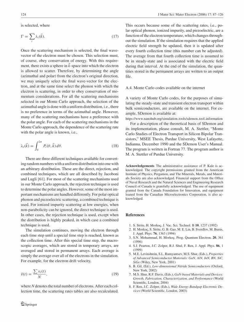
124 J Mater Sci: Mater Electron (2006) 17: 87–126
is selected, where
� =∑
i
λi (�k). (17)
Once the scattering mechanism is selected, the final wave-
vector of the electron must be chosen. This selection must,
of course, obey conservation of energy. With this require-
ment, there exists a sphere in �k-space into which the electron
is allowed to scatter. Therefore, by determining the angle
(azimuthal and polar) from the electron’s original direction,
we may uniquely select the final wave-vector for the elec-
tron, and at the same time select the phonon with which the
electron is scattering, in order to obey conservation of mo-
mentum considerations. For all the scattering mechanisms
selected in our Monte Carlo approach, the selection of the
azimuthal angle is done with a uniform distribution, i.e., there
is no preference in terms of the azimuthal angle. However,
many of the scattering mechanisms have a preference with
the polar angle. For each of the scattering mechanisms in the
Monte Carlo approach, the dependence of the scattering rate
with the polar angle is known, i.e.,
λi (�k) =∫ 2π
0
Pi (θ, �k) dθ. (18)
There are three different techniques available for convert-
ing random numbers with a uniform distribution into one with
an arbitrary distribution. These are the direct, rejection, and
combined techniques, which are all described by Jacoboni
and Lugli [61]. For most of the scattering mechanisms used
in our Monte Carlo approach, the rejection technique is used
to determine the polar angles. However, some of the most im-
portant mechanisms are handled differently. For polar optical
phonon and piezoelectric scattering, a combined technique is
used. For ionized impurity scattering at low energies, when
non-parabolicity can be ignored, the direct technique is used.
In other cases, the rejection technique is used, except when
the distribution is highly peaked, in which case a combined
technique is used.
The simulation continues, moving the electron through
each time step until a special time step is reached, known as
the collection time. After this special time step, the macro-
scopic averages, which are stored in temporary arrays, are
averaged and stored in permanent arrays. Each average is
simply the average over all of the electrons in the simulation.
For example, for the electron drift velocity,
v(t) =∑
vi (t)
N, (19)
where N denotes the total number of electrons. After each col-
lection time, the scattering rates tables are also recalculated.
This occurs because some of the scattering rates, i.e., po-
lar optical phonon, ionized impurity, and piezoelectric, are a
function of the electron temperature, which changes through-
out the simulation. If the simulation requires that the applied
electric field strength be updated, then it is updated after
every fourth collection time (this number can be adjusted).
The average from that fourth collection time is assumed to
be in steady-state and is associated with the electric field
during that interval. At the end of the simulation, the quan-
tities stored in the permanent arrays are written to an output
file.
A.4. Monte Carlo codes available on the internet
A variety of Monte Carlo codes, for the purposes of simu-
lating the steady-state and transient electron transport within
bulk semiconductors, are available on the internet. For ex-
ample, SDemon is available at:
https://www.nanohub.org/simulation tools/sdemon tool information
For a description of the theoretical basis of SDemon and
its implementation, please consult, M. A. Stettler, “Monte
Carlo Studies of Electron Transport in Silicon Bipolar Tran-
sistors,” MSEE Thesis, Purdue University, West Lafayette,
Indianna, December 1990 and the SDemon User’s Manual.
The program is written in Fortran 77. The program author is
M. A. Stettler of Purdue University.
Acknowledgements The administrative assistance of P. Kale is ac-knowledged. The copyright permissions granted from the AmericanInstitute of Physics, Pergamon, and The Minerals, Metals, and Materi-als Society are also acknowledged. Financial support from the Officeof Naval Research and the Natural Sciences and Engineering ResearchCouncil of Canada is gratefully acknowledged. The use of equipmentgranted from the Canada Foundation for Innovation, and equipmentloaned from the Canadian Microelectronics Corporation, is also ac-knowledged.
References
1. S. Strite, H. Morkoc, J. Vac. Sci. Technol. B 10, 1237 (1992)2. H. Morkoc, S. Strite, G. B. Gao, M. E. Lin, B. Sverdlov, M. Burns,
J. Appl. Phys. 76, 1363 (1994)3. S.N. Mohammad, H. Morkoc, Prog. Quantum Electron. 20, 361
(1996)4. S.J. Pearton, J.C. Zolper, R.J. Shul, F. Ren, J. Appl. Phys. 86, 1
(1999)5. M.E. Levinshtein, S.L. Rumyantsev, M.S. Shur, (Eds.), Properties
of Advanced Semiconductor Materials: GaN, AlN, InN, BN, SiC,SiGe (Wiley, New York, 2001)
6. B. Gil, (Ed.), Low-dimensional Nitride Semiconductors (Oxford,New York, 2002)
7. M.S. Shur, R.F. Davis, (Eds.), GaN-based Materials and Devices:Growth, Fabrication, Characterization, and Performance (WorldScientific, London, 2004)
8. F. Ren, J.C. Zolper, (Eds.), Wide Energy Bandgap Electronic De-vices (World Scientific, London, 2003)
Springer

J Mater Sci: Mater Electron (2006) 17: 87–126 125
9. S.J. Pearton, C.R. Abernathy, F. Ren, Gallium Nitride Processingfor Electronics, Sensors and Spintronics (Springer-Verlag, Berlin,2006)
10. M.S. Shur, M.A. Khan, Mater. Res. Soc. Bull. 22(2), 44 (1997)11. M.A. Khan, J.W. Yang, W. Knap, E. Frayssinet, X. Hu, G. Simin,
P. Prystawko, M. Leszczynski, I. Grzegory, S. Porowski, R. Gaska,M.S. Shur, B. Beaumont, M. Teisseire, G. Neu, Appl. Phys. Lett.76, 3807 (2000)
12. X. Hu, J. Deng, N. Pala, R. Gaska, M.S. Shur, C.Q. Chen, J. Yang,G. Simin, M.A. Khan, J.C. Rojo, L.J. Schowalter, Appl. Phys. Lett.82, 1299 (2003)
13. W. Lu, V. Kumar, E.L. Piner, I. Adesida, IEEE Trans. ElectronDevices 50, 1069 (2003)
14. A. Jimenez, Z. Bougrioua, J.M. Tirado, A.F. Brana, E. Calleja, E.Munoz, I. Moerman, Appl. Phys. Lett. 82, 4827 (2003)
15. A.A. Burk, Jr., M.J. O’Loughlin, R.R. Siergiej, A.K. Agarwal,S. Sriram, R.C. Clarke, M.F. MacMillan, V. Balakrishna, C.D.Brandt, Solid-State Electron. 43, 1459 (1999)
16. S. Karmalkar, M.S. Shur, R. Gaska, in Wide Energy Bandgap Elec-tronic Devices, edited by F. Ren and J.C. Zolper, (World Scientific,London, 2003) pp. 173–216.
17. S. Nakamura, Mater. Res. Soc. Bull. 22(2), 29 (1997)18. S.F. Chichibu, S. Nakamura, (Eds.), Nitride Semiconductor Blue
Lasers and Light Emitting Diodes (Taylor and Francis, New York,2000)
19. S. Nakamura, S. Pearton, G. Fasol, The Blue Laser Diode: TheComplete Story, 2nd. ed. (Springer-Verlag, New York, 2000)
20. M. Umeno, T. Egawa, H. Ishikawa, Mater. Sci. Semicond. Process.4, 459 (2001)
21. A. Krost, A. Dadgar, Phys. Status Solidi A 194, 361 (2002)22. A. Zukauskas, M.S. Shur, R. Gaska, Introduction to Solid-State
Lighting (Wiley, New York, 2002)23. C.L. Tseng, M.J. Youh, G.P. Moore, M.A. Hopkins, R. Stevens,
W.N. Wang, Appl. Phys. Lett. 83, 3677 (2003)24. M.S. Shur, A. Zukauskas, (Eds.), UV Solid-State Light Emitters
and Detectors (Kluwer, Boston, 2004)25. J.C. Carrano, A. Zukauskas, (Eds.), Optically Based Biological
and Chemical Sensing for Defense (SPIE, Bellingham, 2004)26. M.A. Littlejohn, J.R. Hauser, T.H. Glisson, Appl. Phys. Lett. 26,
625 (1975)27. D.K. Ferry, Phys. Rev. B 12, 2361 (1975)28. P. Das, D.K. Ferry, Solid-State Electron. 19, 851 (1976)29. B. Gelmont, K. Kim, M. Shur, J. Appl. Phys. 74, 1818
(1993)30. V.W.L. Chin, T.L. Tansley, T. Osotchan, J. Appl. Phys. 75, 7365
(1994)31. N.S. Mansour, K.W. Kim, M.A. Littlejohn, J. Appl. Phys. 77, 2834
(1995)32. J. Kolnık, I.H. Oguzman, K.F. Brennan, R. Wang, P.P. Ruden, Y.
Wang, J. Appl. Phys. 78, 1033 (1995)33. M. Shur, B. Gelmont, M.A. Khan, J. Electron. Mater. 25, 777
(1996)34. B.E. Foutz, L.F. Eastman, U.V. Bhapkar, M.S. Shur, Appl. Phys.
Lett. 70, 2849 (1997)35. U.V. Bhapkar, M.S. Shur, J. Appl. Phys. 82, 1649 (1997)36. S.K. O’Leary, B.E. Foutz, M.S. Shur, U.V. Bhapkar, L.F. Eastman,
J. Appl. Phys. 83, 826 (1998)37. S.K. O’Leary, B.E. Foutz, M.S. Shur, U.V. Bhapkar, L.F. Eastman,
Solid State Commun. 105, 621 (1998)38. J.D. Albrecht, R.P. Wang, P.P. Ruden, M. Farahmand, K.F.
Brennan, J. Appl. Phys. 83, 1446 (1998)39. N.G. Weimann, L.F. Eastman, D. Doppalapudi, H.M. Ng, T.D.
Moustakas, J. Appl. Phys. 83, 3656 (1998)40. J.D. Albrecht, R.P. Wang, P.P. Ruden, M. Farahmand, K.F.
Brennan, J. Appl. Phys. 83, 4777 (1998)
41. E. Bellotti, B.K. Doshi, K.F. Brennan, J.D. Albrecht, P.P. Ruden,J. Appl. Phys. 85, 916 (1999)
42. B.E. Foutz, S.K. O’Leary, M.S. Shur, L.F. Eastman, J. Appl. Phys.85, 7727 (1999)
43. S.K. O’Leary, B.E. Foutz, M.S. Shur, L.F. Eastman, Solid StateCommun. 118, 79 (2001)
44. T.F. de Vasconcelos, F.F. Maia, Jr., E.W.S. Caetano, V.N. Freire,J.A.P. da Costa, E.F. da Silva, Jr., J. Cryst. Growth 246, 320 (2002)
45. S.K. O’Leary, B.E. Foutz, M.S. Shur, L.F. Eastman, J. Electron.Mater. 32, 327 (2003)
46. M. Wraback, H. Shen, J.C. Carrano, T. Li, J.C. Campbell,M.J. Schurman, I.T. Ferguson, Appl. Phys. Lett. 76, 1155(2000)
47. S. Krishnamurthy, M. van Schilfgaarde, A. Sher, A.-B. Chen,Appl. Phys. Lett. 71, 1999 (1997)
48. D.K. Ferry, C. Jacoboni, (Eds.), Quantum Transport in Semicon-ductors (Plenum Press, New York, 1992)
49. N.W. Ashcroft, N.D. Mermin, Solid State Physics (Saunders Col-lege, Philadelphia, 1976)
50. P.A. Sandborn, A. Rao, P.A. Blakey, IEEE Trans. Electron Devices36, 1244 (1989)
51. D.C. Look, J.R. Sizelove, S. Keller, Y.F. Wu, U.K. Mishra, S.P.DenBaars, Solid State Commun. 102, 297 (1997)
52. N.A. Zakhleniuk, C.R. Bennett, B.K. Ridley, M. Babiker, Appl.Phys. Lett. 73, 2485 (1998)
53. B.R. Nag, Electron Transport in Compound Semiconductors(Springer-Verlag, Berlin, 1980)
54. M.S. Krishnan, N. Goldsman, A. Christou, J. Appl. Phys. 83, 5896(1998)
55. R. Oberhuber, G. Zandler, P. Vogl, Appl. Phys. Lett. 73, 818(1998)
56. By an equilibrium state, however, we are not necessarily referringto thermal equilibrium, thermal equilibrium only being achievedin the absence of an applied electric field.
57. By electron drift velocity, we are referring to the average elec-tron velocity, determined by statistically averaging over the entireelectron ensemble.
58. A. Papoulis, Probability, Random Variables, and Stochastic Pro-cesses, 3rd ed. (McGraw-Hill, New York, 1991)
59. W. Fawcett, A.D. Boardman, S. Swain, J. Phys. Chem. Solids 31,1963 (1970)
60. C. Kittel, Introduction to Solid State Physics, 8th ed. (Wiley, NewYork, 2005)
61. C. Jacoboni, P. Lugli, The Monte Carlo Method for SemiconductorDevice Simulation (Springer-Verlag, New York, 1989)
62. B.K. Ridley, Quantum Processes in Semiconductors, 3rd. ed. (Ox-ford, New York, 1993)
63. M. Shur, Physics of Semiconductor Devices (Prentice Hall, En-glewood Cliffs, 1990)
64. P. Lugli, D.K. Ferry, IEEE Trans. Electron Devices 32, 2431 (1985)65. K. Seeger, Semiconductor Physics: An Introduction, 9th ed.
(Springer-Verlag, Berlin, 2004)66. The longitudinal and transverse sound velocities are equal to
√Cl
ρand
√Ct
ρ,
respectively, where Cl and Ct denote the respective elastic con-stants and ρ represents the density. Values for the constants, Cl
and Ct , have been taken from Chin et al. [30].67. Our nominal selection of 0.11 me for the m∗ effective mass as-
sociated with InN was drawn from the review article of Mo-hammad and Morkoc [3], who cited the work of Tyagai et al.[68, 69].
Springer

126 J Mater Sci: Mater Electron (2006) 17: 87–126
68. V.A. Tyagai, A.M. Evstigneev, A.N. Krasiko, A.F. Andreeva, V.Y.Malakhov, Sov. Phys. Semicond. 11, 1257 (1977)
69. V.A. Tyagai, O.V. Snitko, A.M. Evstigneev, A.N. Krasiko, Phys.Status Solidi B 103, 589 (1981)
70. Piezoelectric scattering is treated using the well establishedzincblende scattering rates, and thus, a suitably transformed piezo-electric constant, e14, must be selected. This may be achievedthrough the transformation suggested by Bykhovski et al. [71, 72].The e14 values selected for bulk wurtzite GaN and bulk wurtziteInN are those suggested by Chin et al. [30]. The e14 value se-lected for bulk wurtzite AlN is that suggested by O’Leary et al.[37].
71. A. Bykhovski, B. Gelmont, M. Shur, A. Khan, J. Appl. Phys. 77,1616 (1995)
72. A.D. Bykhovski, V.V. Kaminski, M.S. Shur, Q.C. Chen, M. A.Khan, Appl. Phys. Lett. 68, 818 (1996)
73. H.P. Maruska, J.J. Tietjen, Appl. Phys. Lett. 15, 327 (1969)74. W.M. Yim, E.J. Stofko, P.J. Zanzucchi, J.I. Pankove, M. Ettenberg,
S.L. Gilbert, J. Appl. Phys. 44, 292 (1973)75. T.L. Tansley, C.P. Foley, J. Appl. Phys. 59, 3241 (1986).76. All intervalley deformation potentials are set to 109 eV/cm, fol-
lowing the approach of Gelmont et al. [29].77. We follow the approach of Bhapkar and Shur [35], and set the inter-
valley phonon energies equal to the polar optical phonon energy, arelationship which holds approximately for gallium arsenide [78].
78. M.A. Littlejohn, J.R. Hauser, T.H. Glisson, J. Appl. Phys. 48, 4587(1977)
79. W.R.L. Lambrecht, B. Segall, in Properties of Group III Nitrides,No. 11 EMIS Datareviews Series, edited by J.H. Edgar (Inspec.London, 1994), Chapter 4
80. J.S. Blakemore, J. Appl. Phys. 53, R123 (1982)81. K. Osamura, S. Naka, Y. Murakami, J. Appl. Phys. 46, 3432 (1975)82. V.Y. Davydov, A.A. Klochikhin, V.V. Emtsev, S.V. Ivanov, V.V.
Vekshin, F. Bechstedt, J. Furthmuller, H. Harima, A.V. Mudryi,A. Hashimoto, A. Yamamoto, J. Aderhold, J. Graul, E.E. Haller,Phys. Status Solidi B 230, R4 (2002)
83. J. Wu, W. Walukiewicz, K.M. Yu, J.W. Ager III, E.E. Haller, H.Lu, W.J. Schaff, Y. Saito, Y. Nanishi, Appl. Phys. Lett. 80, 3967(2002)
84. T. Matsuoka, H. Okamoto, M. Nakao, H. Harima, E. Kurimoto,Appl. Phys. Lett. 81, 1246 (2002)
85. K.T. Tsen, C. Poweleit, D.K. Ferry, H. Lu, W.J. Schaff, Appl. Phys.Lett. 86, 222103 (2005)
86. Q.X. Guo, T. Tanaka, M. Nishio, H. Ogawa, X.D. Pu, W.Z. Shen,Appl. Phys. Lett. 86, 231913 (2005)
87. E.G. Brazel, M.A. Chin, V. Narayanamurti, D. Kapolnek, E.J.Tarsa, S.P. DenBaars, Appl. Phys. Lett. 70, 330 (1997)
88. This result is somewhat different from that found earlier byO’Leary et al. [36], as a slightly different InN band structure wasemployed by O’Leary et al. [36].
89. J.D. Albrecht, R. Wang, P.P. Ruden, M. Farahmand, E. Bellotti,K.F. Brennan, Mater. Res. Symp. Proc. 482, 815 (1997)
90. B.E. Foutz, S.K. O’Leary, M.S. Shur, L.F. Eastman, Mater. Res.Symp. Proc. 572, 445 (1999)
91. J.G. Ruch, IEEE Trans. Electron Devices 19, 652 (1972)
92. M.S. Shur, L.F. Eastman, IEEE Trans. Electron Devices 26, 1677(1979)
93. M. Heiblum, M.I. Nathan, D.C. Thomas, C.M. Knoedler, Phys.Rev. Lett. 55, 2200 (1985)
94. A. Palevski, M. Heiblum, C.P. Umbach, C.M. Knoedler, A.N.Broers, R.H. Koch, Phys. Rev. Lett. 62, 1776 (1989)
95. A. Palevski, C.P. Umbach, M. Heiblum, Appl. Phys. Lett. 55, 1421(1989)
96. A. Yacoby, U. Sivan, C.P. Umbach, J.M. Hong, Phys. Rev. Lett.66, 1938 (1991)
97. E. Tiede, M. Thimann, K. Sensse, Chem. Berichte 61, 1568(1928)
98. W.C. Johnson, J.B. Parsons, M.C. Crew, J. Phys. Chem. 36, 2561(1932)
99. R. Juza, H. Hahn, Zeitschr. Anorgan. Allgem. Chem. 239, 282(1938)
100. Z.C. Huang, R. Goldberg, J.C. Chen, Y. Zheng, D.B. Mott, P. Shu,Appl. Phys. Lett. 67, 2825 (1995)
101. L.F. Eastman, V. Tilak, J. Smart, B.M. Green, E.M. Chumbes, R.Dimitrov, H. Kim, O.S. Ambacher, N. Weimann, T. Prunty. M.Murphy, W. J. Schaff, J.R. Shealy, IEEE Trans. Electron Devices48, 479 (2001)
102. C.H. Oxley, M.J. Uren, IEEE Trans. Electron Devices 52, 165(2005)
103. M. Wraback, H. Shen, J.C. Carrano, C.J. Collins, J.C. Campbell,R.D. Dupuis, M.J. Schurman, I.T. Ferguson, Appl. Phys. Lett. 79,1303 (2001)
104. A. Matulionis, J. Liberis, L. Ardaravicius, M. Ramonas,I. Matulioniene, J. Smart, Semicond. Sci. Technol. 17, L9 (2002)
105. C. Bulutay, B.K. Ridley, N.A. Zakhleniuk, Phys. Rev. B 68,115205 (2003)
106. R. Brazis, R. Raguotis, Appl. Phys. Lett. 85, 609 (2004)107. A.A.P. Silva, V.A. Nascimento, J. Lumin. 106, 253 (2004)108. S. Gokden, Physica E 23, 198 (2004)109. B.K. Ridley, W.J. Schaff, L.F. Eastman, J. Appl. Phys. 96, 1499
(2004)110. A. Matulionis, J. Liberis, IEE Proc. - Circ., Dev., and Syst. 151,
148 (2004)111. M. Ramonas, A. Matulionis, J. Liberis, L. Eastman, X. Chen, Y.-J.
Sun, Phys. Rev. B 71, 075324 (2005)112. J.M. Barker, D.K. Ferry, S.M. Goodnick, D.D. Koleske, A. Aller-
man, R.J. Shul, Phys. Status Solidi C 2, 2564 (2005)113. L. Ardaravicius, M. Ramonas, O. Kiprijanovic, J. Liberis, A. Mat-
ulionis, L.F. Eastman, J.R. Shealy, X. Chen, Y.J. Sun, Phys. StatusSolidi A 202, 808 (2005)
114. Y. Chang, K. Y. Tong, C. Surya, Semicond. Sci. Technol. 20, 188(2005)
115. S. Yamakawa, S.M. Goodnick, J. Branlard, M. Saraniti, Phys.Status Solidi C 2, 2573 (2005)
116. A. Reklaitis, L. Reggiani, J. Appl. Phys. 97, 043709 (2005)117. T.V. Shubina, S.V. Ivanov, V.N. Jmerik, M.M. Glazov, A.P.
Kalvarskii, M.G. Tkachman, A. Vasson, J. Leymarie, A. Kavokin,H. Amano, I. Akasaki, K.S.A. Butcher, Q. Guo, B. Monemar, P.S.Kop’ev, Phys. Status Solidi A 202, 377 (2005)
118. R.M. Yorston, J. Comput. Phys. 64, 177 (1986)
Springer