mpc553x, mpc555x, and mpc556x family nexus...
TRANSCRIPT

1 IntroductionThe IEEE-ISTO 5001™-2003 Nexus standard (referred to asthe Nexus standard) interface is an industry standard that crossesCPU boundaries and allows industry-standard tools to supportmultiple CPU architectures. It allows advanced debug capabilitiesby providing high-speed access to the microcontroller core.These advanced debug capabilities include trace, withoutrequiring extensive external circuitry to monitor an externaladdress bus. The Nexus standard defines a minimum feature setthat must be implemented. To simplify discussion of debugcapabilities between different requirements/capabilities, theminimum feature set requirements are divided into four classes.
• Nexus Class 1 defines basic run control capabilities thatmust be implemented.
• A Nexus compliant Class 2 or greater device allowsnon-intrusive instruction and ownership trace on amicrocontroller in single-chip mode or a microcontrollerwithout external data and address buses.
• A Nexus Class 3 or greater device also allows for datatrace and read/write access to memory while themicrocontroller is running.
• Class 4 supports some advanced debug capabilities, butFreescale currently has implemented only a few Class 4features and does not support all of them. Therefore thereare no devices or cores that support the full Class 4requirements.
© Freescale Semiconductor, 2004 – 2010. All rights reserved.
Document Number: AN2614Freescale SemiconductorRev. D, 18/March/2010Application Note
MPC553x, MPC555x, and MPC556xFamily Nexus Interface ConnectorMICTOR-38, Robust, and JTAG Connector Definitions
Randy Deesby:Applications EngineeringAustin,TxUSA
ContentsIntroduction...........................................................11
MPC5500 Nexus Architectural Overview.............22
Nexus Connector Recommendation and Pin-OutDefinitions.............................................................3
3
Nexus Signals for the MPC5500 Family...............94
Nexus Connector Voltages for the MPC5500......145
JTAG Clock Speed for MPC5500.......................156
Minimum External Circuitry...............................157
Nexus Port Configuration Register.....................168
MPC5500 Available Debug Adapters..................19A
Core Memory Access versus Nexus Read/WriteAccess ................................................................20
B
NOTEIn general, Freescale has implemented the Nexus Read/Write Access (RWA) mechanism in all devices usingthe Nexus interface, regardless of whether the device supports Nexus Class 1, Class 2, or Class 3, even thoughRWA is a Class 3 feature. In addition, all e200zx Nexus clients that support trace also implement the NexusClass 4 feature of enabling and disabling of trace upon occurrence of a watchpoint. As these are features thatare above the basic requirements of a given class, generally, these are referred to as a "+" feature. In otherwords, for a client that support all Nexus class 2 features and supports RWA, the implementation is referredto as Class 2+.
The MPC5554 microcontroller was the first device in the MPC5500 family that contained multiple Nexus clients that communicateover a single IEEE-ISTO 5001™-2003 Nexus Combined JTAG IEEE 1149.1/Auxiliary Out interface. When combined, all ofthe Nexus clients are referred to as the Nexus Development Interface (NDI). Class 3 Nexus allows for Program, Data, andOwnership Trace of the MPC5500 device execution without access to the external data and address buses.
This application note addresses the connector options and recommendations for the MPC5554 and other members of theMPC5500 family, including the MPC5533, MPC5534, MPC5553, MPC5561, MPC5565, MPC5566, and MPC5567. While theconnector definitions for the MPC5510 family of devices or any newer MPC56xx families of devices may be the same, someoperations may be slightly different and have different requirements.
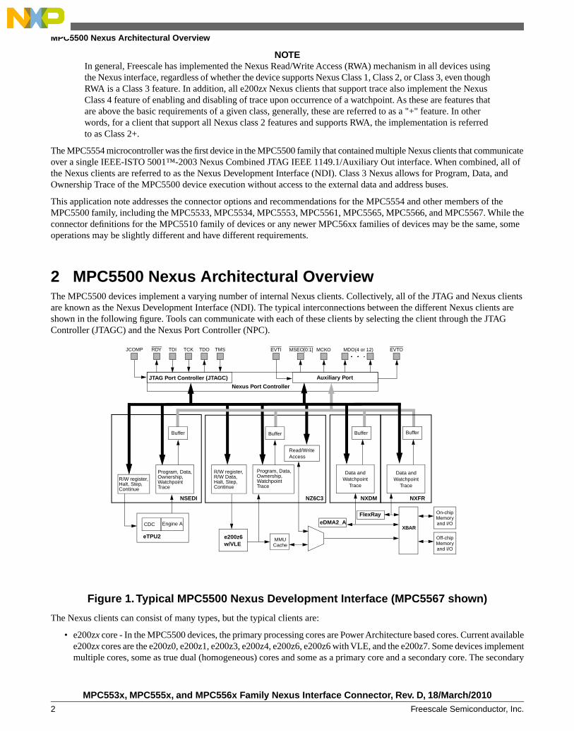
2 MPC5500 Nexus Architectural OverviewThe MPC5500 devices implement a varying number of internal Nexus clients. Collectively, all of the JTAG and Nexus clientsare known as the Nexus Development Interface (NDI). The typical interconnections between the different Nexus clients areshown in the following figure. Tools can communicate with each of these clients by selecting the client through the JTAGController (JTAGC) and the Nexus Port Controller (NPC).
MMUCache
NZ6C3 NXDM
XBAR
On-chipMemoryand I/O
Off-chipMemoryand I/O
RDY TDI TCK TDO TMS EVTI MSEO[0:1] MCKO MDO(4 or 12) EVTOJCOMP
NXFR
R/W register,Halt, Step,Continue
Program, Data,Ownership,WatchpointTrace
eDMA2_A
Data andWatchpoint
Trace
Data andWatchpoint
Trace
Read/WriteAccess
Buffer Buffer Buffer Buffer
Program, Data,Ownership,WatchpointTrace
R/W register,R/W Data,Halt, Step,Continue
e200z6w/VLE
JTAG Port Controller (JTAGC) Auxiliary Port
Nexus Port Controller
NSEDI
FlexRay
eTPU2
Engine ACDC
Figure 1.Typical MPC5500 Nexus Development Interface (MPC5567 shown)
The Nexus clients can consist of many types, but the typical clients are:
• e200zx core - In the MPC5500 devices, the primary processing cores are Power Architecture based cores. Current availablee200zx cores are the e200z0, e200z1, e200z3, e200z4, e200z6, e200z6 with VLE, and the e200z7. Some devices implementmultiple cores, some as true dual (homogeneous) cores and some as a primary core and a secondary core. The secondary
MPC553x, MPC555x, and MPC556x Family Nexus Interface Connector, Rev. D, 18/March/2010Freescale Semiconductor, Inc.2
MPC5500 Nexus Architectural Overview

core is a smaller core intended for off-loading the primary core. The Nexus client is usually named for the core that itsupports plus the Nexus class that the client supports. For example, the Nexus client for the e200z4 that supports Class 3functionality is called the NZ4C3.
• eTPU - The Enhanced Timing Processor (eTPU or eTPU2) is a task-specific computing engine that is designed primarilyfor dealing with timing functions and includes some mathematics capabilities (including multiplication and division). TheeTPU Nexus client is implemented as either a dual eTPU engine (Nexus Dual eTPU Development Interface - NDEDI)or a single eTPU engine client (Nexus Single eTPU Development Interface - NSEDI). In addition to the eTPU engineinterface, the NDEDI/NSEDI interfaces with a secondary Nexus client, the Coherent Data-Parameter Controller (CDC).The CDC supports the shared memory and logic between the dual eTPU engines. On NDEDI devices, the eTPU Nexusinterface appears to have three sub-clients (the two eTPU engines and the CDC). On NSEDI devices there are two (oneengine and the CDC).
• Bus Trace Clients - Another trace client available is a Nexus client that traces data accesses made through a Crossbar busport. Usually, these have been implemented on the master side of the crossbar switch for the eDMA module and theFlexRay Communication Interface. This allows master accesses made by these bus masters to peripherals or memoryaccessed though the Crossbar switch bus (XBAR). Freescale has chosen to implement these interfaces on the master sideof the crossbar for most devices, but this module can also be instantiated on the slave side of the crossbar switch on futuredevices, allowing trace of all accesses into a particular slave port of the crossbar switch bus. Bus trace clients are referencedby the the type of interface they support. For example, the Nexus eDMA Master XBAR client is referred to as the NXDM;the FlexRay Master XBAR trace client is the NXFR.
2.1 Nexus Class 1 JTAG-Only OperationFor Nexus class 1 (run control only) operation, the JTAG pins can be used for standard, stopped mode debug operations. In thismode, Nexus does not have to be enabled and the auxiliary port pins can be ignored by the debugger. Since there is no JTAGstandard connector pin-out definition, Freescale recommends that class 1 only debuggers use the same connector options as fullNexus debuggers. This allows customers to avoid putting two separate connectors on boards for Nexus versus JTAG-only debugtools. However, this document includes a definition for a 14-pin BERG style connector (2 x 7, 0.1" pin centers) for extremelylow-cost applications that cannot use one of the full Nexus connectors.
NOTEThe Nexus Class 3 feature read/write access is accessible through a JTAG connection. OtherClass 3 features are not available unless a full Nexus connector is used.
NOTEIt is recommended that all the full Nexus signals be made available (somewhere) onproduction boards to facilitate debugging new boards and analysis of errors in software,even on boards that have restricted space and provide a JTAG-only connection. If all of theNexus signals are available on the production board, an adapter could be built to provide aNexus connection on boards that do not have a complete footprint for one of the standardNexus connectors; likewise, the JTAG connector does not have to be populated on productionboards. It could even use a smaller connector footprint. This could be used with an adapterto the standard debug connections.
3 Nexus Connector Recommendation and Pin-Out DefinitionsFor the MPC5500 family, Freescale recommends that a single 38-pin MICTOR connector be used on all boards for both reduced-and full-port Nexus modes (M38C). In cases where a more robust connector is required, Freescale recommends that the 51-pinGlenair connector be used (R51C).
The table below shows the possible connectors that can be used for the MPC5500 family devices.
MPC553x, MPC555x, and MPC556x Family Nexus Interface Connector, Rev. D, 18/March/20103Freescale Semiconductor, Inc.
Nexus Connector Recommendation and Pin-Out Definitions

Table 1. Recommended Nexus Connectors for the MPC5500 Family
Maximum message data outsignals (per Nexus standard)
Total number ofpins
Part number (for targetsystem)
DesignationConnector
8 (12 by extension)238 (+ 5)767054-11M38C3M MICTOR
1676 (+ 10)767054-11 X 2M38-2C3M MICTOR
8 (12 by extension)251MR7580-51P2BNUR51CGlenair MicroD Robust
1. Other compatible part numbers are 2-5767004-2 (RoHS compliant), 2-767004-2, 767061-1, and 767044-1.2. Although the Nexus standard definition normally only allows eight MDO signals, Freescale has extended the definition toinclude an extra four MDO signals.
Since full-port mode requires twelve MDO pins and both of these connectors support only eight MDO pins, some of theVendor_IO and Tool_IO pins must be defined for MDO signals (MDO[8:11]). The MICTOR option has five vendor-definedpins (four for the extra MDO signals and then one extra pin), but the 51-pin robust connector only has three Vendor_IO pins.Therefore, to support the full twelve MDO signals, two Tool_IO pins had to be defined as MDO signals. The table below showsthe recommended signal usage for the vendor-defined I/O pins, as well as tool vendor-defined I/O pins. Freescale has workedwith tool vendors to insure minimal impact to tool needs on these pins.
Table 2. Extended MDO definition to the Nexus Standard Connector using IO for additionalMDO Signals
MPC5500 robust definitionMPC5500 MICTOR definitionNexus pin designation
MDO9/GPIO80MDO9/GPIO80VEN_IO0
MDO11/GPIO82MDO11/GPIO82VEN_IO1
RSTOUT1BOOTCFG1/IRQ3/GPIO212VEN_IO2
-2MDO8/GPIO70VEN_IO3
-MDO10/GPIO81VEN_IO4
--3TOOL_IO0
-TOOL_IO1
MDO8/GPIO70-TOOL_IO2
MDO10/GPIO81RSTOUTTOOL_IO3
1. This pin has been redefined since the original definition in 2004. Customers may want to make this signal selectable (via a 0ohm resistor option) between RSTOUT and BOOTCFG1/IRQ3/GPIO212.2. This signal is not available on the 51-pin robust connector3. This pin is defined for use by tool vendors and has no defined connection to the MPC5500 device for the MICTOR connectoroption.
3.1 Port Width Considerations
The 5001-2003 Nexus standard allows the Nexus Auxiliary Output Port to have 01-16 message data outputs (MDO) pins. TheMPC5500 family have two options for Nexus port widths; reduced-port mode has four MDO pins and full-port mode has twelveMDO pins. All levels (Class 1, 2, and 3) of Nexus trace can be supported over either port width, but the reduced port widthlimits the bandwidth available for trace information.
The 5001-2003 allows for a zero-width auxiliary output port to support Class 3 features by embedding the auxiliary outputdata into a specially formatted JTAG message. The MPC5500 devices do not support embedding trace information in a JTAGmessage.
1.
MPC553x, MPC555x, and MPC556x Family Nexus Interface Connector, Rev. D, 18/March/2010Freescale Semiconductor, Inc.4
Nexus Connector Recommendation and Pin-Out Definitions

Table 3. MPC5500 Family Nexus Port Width
Number of MDO SignalsPort Mode
4Reduced Port Mode (RPM)
12Full Port Mode (FPM)
The table below shows the port widths available in each of the possible package types for the currently defined members of theMPC5500 family.
Table 4. MPC5500 Family Nexus Port Width Options
Full Auxiliary Port Available/SizeReduced Auxiliary Port Available /SizePackage Size (Balls)
No / 0Yes / 4208
Yes / 12Yes / 4324
Yes / 12Yes / 4416
Yes / 12Yes / 44961
1.The 496 package is not a standard production package that can be purchased by customers. It is used in the VertiCal emulationdevice.
3.2 MPC5500 JTAG ConnectorThe figure below shows the pinout of the recommended JTAG connector to support the MPC5500 devices. If there is enoughroom allowed in the target system, a full Nexus connector is preferred over the simple 14-pin JTAG connector since it allowsa higher degree of debug capability. It can be used as a minimum debug access or for BSDL board testing.
The recommended connector for the target system is the Tyco part number 2514-6002UB.
NOTEThis pinout is similar to the Freescale MCORE and DSP JTAG/OnCE connector definitions.
Table 5. Recommended JTAG Connector Pinout
DescriptionPinPinDescription
GND21TDI
GND43TDO
GND65TCK
-87EVTI1
TMS109RESET
GND1211VREF
JCOMP1413RDY2
1. EVTI is optional and was not included in the original (very early) definitions of the JTAG-only connector.2. The RDY signal is not available on all packages or on all devices. Check the device pinout specification. In general it is notavailable in packages with 208 signals or less.
NOTEFreescale recommends that a full Nexus connector be used for all tool debug connectionsregardless of whether Nexus trace information is needed. Adapters for a JTAG Class 114-pin connector (tool side) to the full Nexus MICTOR connectors (board side) are availablefrom P&E Microcomputer Systems (http://www.pemicro.com), part number PE1906, andfrom Lauterbach (http://www.lauterbach.com), order number LA-3723
MPC553x, MPC555x, and MPC556x Family Nexus Interface Connector, Rev. D, 18/March/20105Freescale Semiconductor, Inc.
Nexus Connector Recommendation and Pin-Out Definitions

(CON-JTAG14-MICTOR). Lauterbach also has an adapter that will connect a MICTORconnector (tool side) to a 14-pin JTAG connector (board side). This adapter is order numberLA-3725 (CON-MIC38-J14-5500).
3.3 MICTOR Connector Definition for the MPC5500 FamilyThe following table shows the complete signal usage for the MPC5500 full-port mode MICTOR connector. This uses theVendor_IO pins 1–4 as MDO[11:8]. This connector may also be used for reduced-port mode (which only uses MDO[3:0]).While only one MICTOR is recommended, some tools may not support this configuration. For maximum tool compatibility, asecond MICTOR may need to be added for the upper four MDO signals (MDO[11:8]). If the second connector is used, thelayout of the two connectors should conform to the dimensions in the figure following the tables.
Table 6. MPC5500 Family MICTOR Connector M38C
MPC5500 signalCombined M38Cor M38-2C
Combined M38Cor M38-2C
MPC5500 signal
-Reserved1-2
Gro
und1-Reserved1-
-Reserved1-43-Reserved1-
CLKOUTCLOCKOUTOut65OutVEN_IO0MDO9/GPIO80
MDO8/GPIO70VEN_IO3Out87InVEN_IO2BOOTCFG1/IRQ3/GPIO212
EVTI/EVTIIn109In/RESETRESET
VDDE7VTREF1211OutTDOTDO
RDY/RDYOut1413OutVEN_IO4MDO10/GPIO81
MDO7/GPIO78MDO7Out1615InTCKTCK
MDO6/GPIO77MDO6Out18
Gro
und17InTMSTMS
MDO5/GPIO76MDO5Out2019TDITDI
MDO4/GPIO75MDO4Out2221In/TRSTJCOMP
MDO3MDO3Out24
Gro
und23OutVEN_IO1MDO11/GPIO82
MDO2MDO2Out2625OutTOOL_IO3RSTOUT
MDO1MDO1Out2827TOOL_IO2-2
MDO0MDO0Out3029TOOL_IO1-2
EVTO/EVTOOut3231UBATT12 volts
MCKOMCKOOut3433UBATT12 volts
MSEO1/MSEO1Out3635TOOL_IO0-2
MSEO0/MSEO0Out3837VALTREFVSTBY
1. Pins 1 through 4 should be considered "reserved" and may be used by some logic analyzers as ground connections. If careis taken (and the proper cables are used), these pins could be used for customer I/O signals. However, check with the toolvendors used.2. This optional Nexus signal is defined for use by tool vendors and has no defined connection to the MPC5500 family device.
MPC553x, MPC555x, and MPC556x Family Nexus Interface Connector, Rev. D, 18/March/2010Freescale Semiconductor, Inc.6
Nexus Connector Recommendation and Pin-Out Definitions

Table 7. MPC5500 Family MICTOR Connector M38-2C (Second Half, if needed)
MPC5500 SignalCombined M38-2C
Combined M38-2C
MPC5500 Signal
-Reserved-2
Gro
und1-Reserved-
-Reserved-43-Reserved-
---65In/OutVEN_IO5-
-PORT15In/Out87In/OutVEN_IO6-
-PORT14In/Out109In/OutVEN_IO7-
-PORT13In/Out1211In/OutVEN_IO8-
-PORT12In/Out1413In/OutVEN_IO9-
-PORT11In/Out1615In/OutTOOL_IO7-
-PORT10In/Out18
Gro
und17In/OutTOOL_IO6-
-PORT9In/Out2019In/OutTOOL_IO5-
-PORT8In/Out2221In/OutTOOL_IO4-
-PORT7In/Out24G
roun
d23OutMDO15
-PORT6In/Out2625OutMDO14
-PORT5In/Out2827OutMDO13
-PORT4In/Out3029OutMDO12
-PORT3In/Out3231OutMDO11MDO11/GPIO821
-PORT2In/Out3433OutMDO10MDO10/GPIO812
-PORT1In/Out3635OutMDO9MDO9/GPIO803
-PORT05In/Out3837OutMDO8MDO8/GPIO794
1. This pin duplicates the signal available on pin 23 of the first MICTOR connector.2. This pin duplicates the signal available on pin 13 of the first MICTOR connector.3. This pin duplicates the signal available on pin 8 of the first MICTOR connector.4. This pin duplicates the signal available on pin 7 of the first MICTOR connector.5. The MPC5500 family does not support port replacement.
The following figure shows the recommended layout for the M38-2C connectors. This spacing should be adhered to if the twoMICTOR connector option is implemented in the target system.
MPC553x, MPC555x, and MPC556x Family Nexus Interface Connector, Rev. D, 18/March/20107Freescale Semiconductor, Inc.
Nexus Connector Recommendation and Pin-Out Definitions

Target PCB1
M38CM38-2C 0.75 inch
[19.05 mm]
1
Figure 2. Nexus M38-2C Connector Layout
3.4 Robust Connectors for the MPC5500The robust connectors are designed to be used in harsh environments such as under the hood of an automobile. The robustconnectors listed in Table 3 are manufactured by Glenair, Inc. and feature TwistPin connections for highly reliable contactunder all conditions in a Micro-D configuration. The figure below is an illustration of a typical sub-D configuration and aclose-up of the TwistPin, and is provided courtesy of Glenair, Inc (http://www.glenair.com).
Figure 3. Details of the Glenair Micro-D TwistPin Connectors
Normally, a 100-pin Glenair Micro-D connector should be defined for a Nexus device with more than eight MDO pins. However,due to board area and cost, Freescale recommends the 51-pin Glenair Micro-D connector be used with the MPC5500. The tablebelow shows the recommended pinout for the robust connector option. It is similar to the R51C connector (which supports upto eight MDO pins), but it redefines the Vendor_IO and Tool_IO pins for use as four additional MDO signals (see Figure 5).
MPC553x, MPC555x, and MPC556x Family Nexus Interface Connector, Rev. D, 18/March/2010Freescale Semiconductor, Inc.8
Nexus Connector Recommendation and Pin-Out Definitions

Table 8. MPC5500 Family 51-Pin robust connector definition
1 UBATT19 MDO0
2 UBATT36 GND20 GND
3 VSTBY (VALTREF)37 MDO421 MCKO
4 TOOL_IO038 GND22 GND
5 TDO39 MDO523 EVTO
6RDY40 GND24 GND
7RESET41 MDO625 MSEO0
8 VDDE7 (VREF)42 GND26 MDO9 (VEN_IO0)
9 EVTI43 MDO727 MDO1
10 GND44 GND28 GND
11 JCOMP (TRST)45 MDO8 (TOOL_IO2)29 MDO2
12 GND46 GND30 GND
13 TMS47 MDO10 (TOOL_IO3)31 MDO3
14 GND48 GND32 GND
15 TDI49 MDO11 (VEN_IO1)33 TOOL_IO1
16 GND50 GND34 GND
17 TCK51 RSTOUT135 MSEO1
18 GND
1. For maximum system flexibility, a 0 Ω resistor option could be used to select between the RSTOUT function and theBootCFG1/IRQ3/GPIO212 for this pin for additional debug capabilities.
NOTECLKOUT is not available on the robust 51-pin connector. This may limit some capabilitiesof tools. Tools cannot directly determine the microcontroller's clock speed and mustdetermine the processor speed based on the MCKO frequency and the programmed MCKOdivider ratio.
NOTEIf RSTOUT is on pin 51 of the connector, then the capability of the tool triggering aninterrupt or DMA access will not be available. However, if BOOTCFG1/IRQ3/GPIO212is on pin 51, then the tool cannot determine exactly when an MCU-initiated reset wasasserted.
4 Nexus Signals for the MPC5500 FamilyThe figure below shows a block diagram of the MPC5500 family Nexus signals. The pins are divided between the JTAG/OnCEport, the auxiliary input port, the auxiliary output port, and reference signals. The RDY pin is grouped with the JTAG pins, butit is used for Nexus block transfers done through the JTAG port (read/write messaging).
MPC553x, MPC555x, and MPC556x Family Nexus Interface Connector, Rev. D, 18/March/20109Freescale Semiconductor, Inc.
Nexus Signals for the MPC5500 Family

JTAG
TD
I
TD
O
1 1
AUX Out
TC
K1
TM
S1 1
JCO
MP
1
EV
TI
1
AUX In
4,8,
12,o
r16
1
MD
O
MC
KO
1or
2
1E
VTO
MPC5500/MPC5600
Control and Read/WriteMessage Access
All Program, Data, Ownership and TraceMessages, plus Watchpoint Messages andEvent Triggering
RD
Y
1C
LKO
UT
RE
SE
T1
VE
N_I
O0–
4
VREF
VALTREF
Reference
Note: Dashed signals are optional in the Nexus standard.Tool_IO pins do not have any connectivity to the MCU.
RE
SE
TO
UT
1
MS
EO
Figure 4. Pin interface for an MPC5500 Nexus combined JTAG/AUX port
The auxiliary output port can be implemented with four, eight, twelve, or sixteen Message Data Output signals (MDO) andeither one or two Message Start/End Output signals (MSEO).
Some of the auxiliary output port functions on the MPC5500 family are shared with other pin functions. The following sectionsshow the JTAG and Nexus auxiliary port signals versus the MPC5500 pins and signal descriptions.
4.1 MPC5500 JTAG SignalsThe following table shows the JTAG signals for the MPC5500 families.
Table 9. JTAG Connector Signal Descriptions
DescriptionJTAG Signal
JTAG Test Data Output (TDO). TDO provides the serial test data output for the on-chip testlogic.
TDO
JTAG Test Data Input (TDI). TDI provides the serial test instruction and data input for the on-chip test logic.
TDI
JTAG Test Clock Input (TCK). TCK is the clock input to the JTAG TAP controller and shouldbe a maximum of one-fourth of the system clock frequency.
TCK
JTAG Test Mode Select Input (TMS). TMS controls test mode operations for the on-chip testlogic for boundary scan and debug access.
TMS
Nexus Event In (EVTI). After reset, the EVTI pin is used to initiate program and data tracesynchronization messages or generate a breakpoint. If asserted during reset, upon negationof RESET, the device will enter debug mode and not begin code execution.
EVTI
Nexus Ready Output (RDY). RDY is an output that indicates to the development tools that thedata is ready to be read from or written to the Nexus read/write access registers.
RDY
Reset (RESET). This is the reset input to the microcontroller. It should be driven by tools toreset the microcontroller. It should be driven by an open drain device. The tool should alsomonitor this pin to determine if other devices have forced a reset to the microcontroller. It doesnot reset the JTAG state machine.
RESET
JTAG TAP Controller Enable/ JTAG Compliancy (JCOMP). JCOMP is used to enable theTAP controller for communication to the JTAG state machine for boundary scan and for debug
access. A high on this pin enables the TAP controller.1
JCOMP
MPC553x, MPC555x, and MPC556x Family Nexus Interface Connector, Rev. D, 18/March/2010Freescale Semiconductor, Inc.10
Nexus Signals for the MPC5500 Family

DescriptionJTAG Signal
Nexus VREF (VREF). Provides a reference for the signal levels of the Nexus device. All inputhigh and low voltages should be referenced to this pin.The Nexus specification defines the inputvoltages as VIL = 0.3xVREF and VIH = 0.7xVREF.Note: This is a reference for the signal level and may not be the actual power supply for thedebug pins. See the device definition for the debug pins in the device reference manual.
VREF
Ground. This is the negative reference (return) for the interface.GND
1. The IEEE 1149.1 specifies a Test Reset (TRST) pin; however, the standard defines that by default the pin should be high(enabled) on the device. Since normal operation of the device does not require the JTAG port to be enabled, Freescale uses theJTAG Compliancy pin (JCOMP), which performs the same basic function, but is asserted (low) by default to disable the JTAGboundary scan/debug port (for normal operation).
The recommended voltage of the JTAG connector is a nominal 3.3 volts for the MPC5500 family devices. For the MPC5600family and the MPC5510 family, see the definition in each device's reference manual for the recommended voltage. Somedevices recommend a nominal 3.3 volts and some devices are 5.0 volts.
4.2 Nexus Auxiliary Port SignalsSome of the auxiliary output port functions on the MPC5500 family are shared with other pin functions. The table below showsthe Nexus signal versus the MPC5500/ pins and signal descriptions.
Table 10. Nexus Auxiliary Port Signal Descriptions
DescriptionFull SignalName
MPC5500 SignalNexus SignalSignal Type
EVTO is an output that provides timing to adevelopment tool for a single watchpoint orbreakpoint occurrence.
Nexus EventOut
EVTO/EVTO
Aux
iliar
y O
utpu
t Por
t
The MSEO[1:0] signals indicate when an MDOpacket has started and when an MDO packethas ended.
Nexus Mes-sageStart/End Out-put
MSEO[1:0]/MSEO[1:0]
MCKO provides timing for the MDO andMSEO[0:1] signals.
Nexus Mes-sage ClockOut
MCKOMCKO
MDO[3:0] provide the message data out of theauxiliary output port in the reduced-port config-uration. The full-port configuration usesMDO[11:0].
Nexus Mes-sage DataOutput
MDO11_GPIO82MDO10_GPIO81MDO9_GPIO80MDO8_GPIO70MDO7_GPIO78MDO6_GPIO77MDO5_GPIO76MDO4_GPIO75MDO3MDO2MDO1MDO0
MDO[11:0]
MPC553x, MPC555x, and MPC556x Family Nexus Interface Connector, Rev. D, 18/March/201011Freescale Semiconductor, Inc.
Nexus Signals for the MPC5500 Family

DescriptionFull SignalName
MPC5500 SignalNexus SignalSignal Type
After reset, the EVTI pin is used to initiate pro-gram and data trace synchronization messagesor generate a breakpoint. If asserted duringreset, upon negation of RESET, the device willenter debug mode and not begin code execu-tion.
Nexus EventInput
EVTI/EVTI
Aux
iliar
y In
put P
ort
4.3 Other Nexus Connector SignalsIn addition to the JTAG and Nexus auxiliary port signals, there are additional signals included on the connector for referenceand for use by tools or other purposes. The following table shows the definition of these signals.
Table 11. Other Nexus Connector Signal Descriptions
DescriptionFull SignalName
MPC5500 SignalNexus SignalSignal Type
Nexus Vendor_IO0 (VEN_IO2).The MPC5500signal BOOTCFG1_IRQ3_GPIO212 gives theNexus tool access to IRQ3. This signal caneither generate an interrupt to the interruptcontroller or can be used to initiate a DMAtransfer via DMA channel 3. This allows theNexus port to request a DMA transfer. It canalso invoke the DMA gather data feature. TheBOOTCFG1 function can be used during resetto change the default boot mode of the device.
On the robust connector, this pin is used forRSTOUT.
VendorDefined IO 2
BOOTCFG1_IRQ3_GPIO212VEN_IO2
Ven
dor
IO
MPC553x, MPC555x, and MPC556x Family Nexus Interface Connector, Rev. D, 18/March/2010Freescale Semiconductor, Inc.12
Nexus Signals for the MPC5500 Family
DescriptionFull SignalName
MPC5500 SignalNexus SignalSignal Type
Nexus Tool_IO0 (TOOL_BR). This pin is re-served for use as a bus request signal for arbit-ration between different tools on the Nexus bus.It has no connection to the MPC5500 device.
Note: Tool arbitration is an informal extensionof the Nexus IEEE-ISTO 5001-2003 specifica-tion and has not been approved by the NexusConsortium.
Tool DefinedIO 0
TOOL_IO0
Tool
IO
Nexus Tool_IO1 (TOOL_BG). This pin is re-served for use as a bus grant signal for arbitra-tion between different tools on the Nexus bus.It has no connection to the MPC5500 device.Note: Tool arbitration is an informal extensionof the Nexus IEEE-ISTO 5001-2003 specifica-tion and has not been approved by the NexusConsortium.
Tool DefinedIO 1
TOOL_IO1
Nexus Tool_IO3 (Tool_IO3) This pin is definedon the MICTOR 38 pin connector as RSTOUTof the MPC5500. This allows a tool to monitorwhen the MPC5500 has caused an internalreset.Note: The MCU can drive RSTOUT low viasoftware to reset external devices, but notcause a reset of the MCU.
This pin is defined for use as MDO10 on therobust connector option.
Tool DefinedIO 3
TOOL_IO3
Tool_IO pins (TOOL_IO[4:7]). Designated forNexus tool use. At this time, there are nodefined connections from these pins to theMPC5500 family device. They may be used forcommunication between multiple tools on theNexus connector. These pins are not availableon the single MICTOR connector option or onthe 51-pin robust connector.
Tool DefinedIO [4:7]
TOOL_IO[4:7]
MPC553x, MPC555x, and MPC556x Family Nexus Interface Connector, Rev. D, 18/March/201013Freescale Semiconductor, Inc.
Nexus Signals for the MPC5500 Family

DescriptionFull SignalName
MPC5500 SignalNexus SignalSignal Type
Reset (/RESET). This is the reset input to theMPC5500 microcontroller and should be drivenby tools to reset the microcontroller. It shouldbe driven by an open drain device. The toolshould also monitor this pin to determine ifother devices have forced a reset to the micro-controller. It does not reset the JTAG statemachine.
/ResetRESET/RESET
Ref
eren
ce S
igna
ls
Clock Out (CLKOUT). Clock out provides areference clock for determining the systemclock frequency. The user can disable this sig-nal.
System ClockOutput
CLKOUTCLOCKOUT
Nexus VREF (VREF). Provides a reference forthe signal levels of the Nexus device. All inputhigh and low voltages should be referenced tothis pin. The Nexus specification defines theinput voltages as VIL = 0.3 × VREF andVIH = 0.7 × VREF.
Signal PowerReference
VDDE7VREF
Nexus VALTREF (VSTBY). Provides a monitorfor the backup power supply for theMPC5500family internal SRAM. This pin is monitored bythe Nexus tool to determine if power is lost tothe standby supply of the system. This pinshould be grounded if standby operation is notallowed in a particular system.
Alternate Ref-erence
VSTBYVALTREF
Ground. This is the return (ground) referencepoint for the Nexus connectors. Many groundsignals are included to provide shielding for thehigh-speed Nexus signals. In the MICTORconnector, the center pins should be grounded.
Ground Refer-ence
GNDGND
Battery/unregulated module voltage. This is asupply voltage output from the target systemand should have reverse-bias protection. Thisallows tools to have circuitry powered by thetarget system. The IEEE-ISTO 5001-2003defines this as a 5 to 20 volt supply of up to300 mA of current.
UnregulatedBatteryVoltage
12VUBATT
5 Nexus Connector Voltages for the MPC5500All of the Nexus pins on the MPC5500 family are supplied by VDDE7. VDDE7 can be used with any voltage from 1.62 to 3.6volts. The user determines the voltage level of the Nexus pins. See the following table for the common voltages that could beused. Most commonly, this should be set to 3.3 V, which is also the most common bus voltage used on the MPC5500 family.
Table 12. Nexus Port Voltages Options
Recommended Nexus VoltageSystem Bus Voltage
1.8 volts1.8 volts
2.5 volts2.5 volts
3.3 volts13.3 volts
MPC553x, MPC555x, and MPC556x Family Nexus Interface Connector, Rev. D, 18/March/2010Freescale Semiconductor, Inc.14
Nexus Connector Voltages for the MPC5500

1. A 3.3 V supply is the preferred option. 1.8 V and 2.5 V are not recommended, although they are allowed within the specification.
On the MPC5500, the RESET input should be driven by devices with an open drain. The target system is required to have apullup device to the device power supply. This can be up to 5 V for the MPC5500. Care must be taken to insure that all circuitryconnected to the RESET signal is 5 V tolerant. Tools need to be able to drive RESET, but they also need to sense RESET todetermine if another device in the target system has requested the MCU be reset.
NOTERSTOUT is negated 2400 clocks after RESET is negated or the system PLL is locked(whichever occurs last) in normal clock operating modes (crystal or external reference).RSTOUT is negated 16000 clocks after RESET is negated or the PLL is locked in bypassor 1:1 clock modes.
NOTERESET and RSTOUT are powered by VDDEH6. VDDEH6 can have a nominal voltage of3.3 or 5.0 volts. Other than the UBATT pins, the IEEE-ISTO 5001-2003 standard does notallow voltages greater than VREF. If VDDEH6 is connected to 5.0 volts, then the tool musthave protection for the RESET and RSTOUT signals.
NOTEConsult the hardware specifications of the debug interface to insure that the voltages areall compatible with the module design.
6 JTAG Clock Speed for MPC5500The JTAG/OnCE interface on the MPC5500 devices has a maximum operating frequency of one-fourth of the system frequency.Immediately after reset, the MCU system frequency will be 1.5 times the crystal input (or input frequency). The JTAG/OnCEclock frequency should therefore be set to a maximum of 3 MHz (assuming an 8-MHz crystal, the operating frequency will be12 MHz) until the tool detects that the user has changed the operating frequency of the device. Clock Out (CLKOUT) may bemonitored by the tool initially to determine the system frequency. This clock should not be a requirement for the normal operationof the Nexus interface since the user has the option of disabling this clock.
NOTE
CLKOUT is not available on the robust connector.
7 Minimum External CircuitryIn general, other than the connector, no additional circuitry is required for the Nexus/JTAG debug circuitry. The MPC5500devices include internal pull devices that insure the pins remain in a safe state; however, if there is additional circuitry connectedto the Nexus/JTAG pins or long traces that could affected by other signals (due to crosstalk from high current or high speedsignals), a minimum number of external pull resistors can be added to insure proper operation under all conditions.
Table 13. Optional Minimum Debug Port External Resistors
DescriptionResistor direction andvalue
Nexus/JTAG Signal
Holds debug port in reset and prevents any debug commands from interferingwith the normal operation of the MCU.
10K Ω pull downJCOMP
The RESET input should be driven from an open collector output; therefore,it requires a pullup resistor for the MCU.
4.7K Ω pull upRESET
With no tool attached, this signal should be held low and may or may not beconnected to a pin of the MCU, depending on the system definition.
10K Ω pull downTD/WDT1
MPC553x, MPC555x, and MPC556x Family Nexus Interface Connector, Rev. D, 18/March/201015Freescale Semiconductor, Inc.
JTAG Clock Speed for MPC5500

DescriptionResistor direction andvalue
Nexus/JTAG Signal
A pullup prevents debug mode from being forced after reset if debug modeis enabled (JCOMP = high). It also prevents breakpoints from being forcedif debug mode is enabled.Note: In almost all situations, a resistor is not required on this signal.
10K Ω pull upEVTI
1. This is an optional signal and is not actually required for the MCU.
In addition to the pull resistors, some systems may want to use buffers between the Nexus/JTAG connector inputs and the MCU.This will prevent over-voltage conditions from causing damage to the MCU signals. Normal systems should not require thiscircuitry, but it is helpful in systems that can be exposed to improper connections that provide voltages that are outside the
operating conditions of the MCU. A common circuit to use is the Texas Instruments SN74CBTLV38612. This device is a busswitch that implements a bidirectional interface between two terminals with less than 5 Ω of resistance. It should be poweredby the same supply that powers the debug port. The device enable should be connected to ground for the interface to be enabledwhenever the debug port on the MCU is powered. This circuit provides a high impedance to the tool when the debug port ispowered off.
NOTEIt is recommended that at least the reduced port configuration Nexus signals be madeavailable (somewhere) on production boards. This facilitates debugging of new boards andanalysis of errors in software, even on boards that have restricted space and normally providea JTAG-only connection. If the Nexus signals are available on the production board, anadapter could be built to provide a Nexus connection on boards that do not have a completefootprint for one of the standard Nexus connectors. Likewise, the JTAG connector does nothave to be populated on production boards and could even utilize a smaller connectorfootprint that could be used with an adapter to the standard debug connections.
8 Nexus Port Configuration RegisterThe Nexus Port Controller Port Configuration Register (NPC_PCR) controls the operation and configuration of the Nexus debuginterface for the entire device. This register overrides any control settings (MCKO_DIV, FPM, and MCKO_EN) that may beavailable in individual Nexus client (NDEDI/NSEDI, NZ6C3/NZ3C3, NXDM, and NXFR) Debug Control (DC) or PortConfiguration Registers (PCR).
During RESET, the MPC5500 will assert (high) MDO0 until the PLL is locked after the initial internal power-on reset. OnceMDO0 is negated (low), access to the JTAG controller is enabled and registers can be written by tools. The nexus port shouldbe enabled in the NPC_PCR while the processor is in reset. After the port has been configured, the NPC will transmit a deviceidentification (DID) message through the Nexus auxiliary output port.
NOTEThe numbering of the bits in the NPC_PCR are set per the IEEE-ISTO 5001 standard, asit is accessed only by tools and the CPU cannot write to any of the bits in the register. Allbits are controlled by the external tool.
SN74CBTLV3861-Q1 is automotive qualified if required.2.
MPC553x, MPC555x, and MPC556x Family Nexus Interface Connector, Rev. D, 18/March/2010Freescale Semiconductor, Inc.16
Nexus Port Configuration Register

Table 14. NPC Port Configuration Register (NPC_PCR)
16171819202122232425262728293031
NP
C R
egis
ter
Inde
x 12
7
0000000
NE
XC
FG3
DD
R_E
N2
EV
T_E
N1MCKO_DIV
MC
KO
_EN
MC
KO
_GT
FPMR
W
0000000000000000Reset
0123456789101112131415
PS
TAT_
EN
50000000
LP1_
SY
N4
LP2_
SY
N400000
LP_D
BG
4R
W
0000000000000000Reset
1. This bit is not implemented on all devices. It is not implemented on any of the MPC5500 devices.2. The Double Data Rate feature does not conform to the Nexus 5001 standard and may not be supported.3. Not supported on all devices. This use of this bit is determined by the MCU definition.4. Not supported on devices that do not support true low-power modes (where some power supplies can be removed from theMCU).5. PSTAT is an internal Freescale monitor mechanism and its use is not supported. This bit should always be set to 0.
8.1 MPC5500 Nexus Port Size (NPC_PCR[FPM])The configuration of the full-port mode or reduced-port mode is selected via the JTAG/OnCE port by setting of the Full PortMode (FPM) bit in the Nexus Port Controller port configuration register (NPC_PCR). Setting NPC_PCR[FPM] selects full-portmode. Clearing NPC_PCR[FPM] selects reduced-port mode. In RPM, MDO[4:11] are defined to the GPIO function; FPMautomatically disables the GPIO function.
Table 15. Nexus Port Controller Full Port Mode bit Settings
DescriptionSet-ting
Reduced port mode is selected.0b0
Full port mode is selected.0b1
Table 16. MPC5500 Family Nexus Port Sizes Across Packages
Full Port SizeReduced Port SizePackageDevice
NA14208 MAPBGAMPC5534
124324 PBGA
124324 PBGAMPC5553
124416 PBGA
124416 PBGAMPC5554
124324 PBGAMPC5561
124324 PBGAMPC5565
124416 PBGAMPC5566
MPC553x, MPC555x, and MPC556x Family Nexus Interface Connector, Rev. D, 18/March/201017Freescale Semiconductor, Inc.
Nexus Port Configuration Register

Full Port SizeReduced Port SizePackageDevice
124324 PBGAMPC5567
124416 PBGA
1. Not available.
8.2 Nexus Clock Speed (NPC_PCR[MCKO_DIV])The Nexus auxiliary clock prescaler should be programmed in the NPC_PCR. For systems with a maximum operating frequencyof over 80 MHz, the auxiliary clock prescaler should be set to divide by 2 or more. MCKO_DIV should not be changed afterthe auxiliary output port is enabled (NPC_PCR[MCKO_EN]). The ability to run the MCKO at the same frequency as the systemfrequency is available on some devices if the system frequency is 80 MHz or less. In all cases, see the device electrical specificationto determine if the signals have any other speed limitations.
Table 17. Nexus MCKO Clock Divider Options
MCKO FrequencyMCKO_DIV
System Frequency10b000
System frequency ÷ 20b001
Reserved0b010
System frequency ÷ 40b011
Reserved0b100
Reserved0b101
Reserved0b110
System frequency ÷ 80b111
1. The 1X clock mode is not supported on all devices. In addition, MCKO is limited to 80 MHz maximum on all devices.
The speed of the Nexus port limits the amount of trace information that will be available to tools. Enabling too much trace willcause overflows of the trace buffers included on the device. In general, trace of the core program execution will not causeoverflows with the MCKO frequency set to divide by two. A divide of four may also support full instruction trace if branchhistory mode is used. Enabling data trace may cause overruns if too much information is requested. Care should be taken whenenabling data trace to limit the information that should be traced. Watchpoints can be used to enable trace upon an eventoccurrence and then disabled by a second event to limit the data trace bandwidth requirements.
8.3 Nexus Clock Gating (NPC_PCR[MCKO_GT])The Nexus auxiliary output clock (MCKO) can be gated off when the MPC5500 is not transmitting trace information. SettingNPC_PCR[MCKO_GT] gates the auxiliary clock off when auxiliary messages are not being transmitted. If this bit is cleared,then the Nexus auxiliary clock is always present when the Nexus auxiliary port is enabled.
NOTETools may require that the MCKO not be gated. Check with your tool vendor to determineif the tool can work with a gated MCKO.
8.4 Unsupported Bits in the NPC_PCRNone of the MPC5500 devices covered by this application note support low power modes. Therefore the Low Power DebugEnable (LP_DBG) and the Low Power Mode Synchronization (LP2_SYN and LP1_SYN) bits in the NPC_PCR are not supported.In addition, none of the devices implement or use the Nexus Configuration Select (NEXCFG) bit in the NPC_PCR.
MPC553x, MPC555x, and MPC556x Family Nexus Interface Connector, Rev. D, 18/March/2010Freescale Semiconductor, Inc.18
Nexus Port Configuration Register

The Event Enable (EVT_EN - for enabling/disabling of the EVTI and EVTO.
The Dual Data Rate (DDR) enables a non-standard signal format that clocks two bits per clock cycle. The MDO bits are validapproximately halfway between the falling and rising edges of MCKO and then again between the rising and falling edges ofMCKO. This convention is not covered by the IEEE-ISTO5001 standard and is not expected to be supported by the standard.
The Nexus Configuration (NEXCFG) bit is not supported on any of the MPC5500 devices.
The Processor Status Enable (PSTAT_EN) is not supported on any devices. This is an internal mode for Freescale use only.
Appendix A MPC5500 Available Debug AdaptersA number of adapters are available to ease the task of having full debug capabilities available with a minimum board footprintimpact to the target system. The following table lists adapters that are available from Freescale and third-party manufacturers.
Table A-1. Available Debug Connector Adapters
ManufacturerDescriptionPart Number
P&E Microcomputer Systems14-pin JTAG debug tool to MICTOR 38-pin target board con-nector adapter
PE1906
Lauterbach GmbH14-pin JTAG debug tool to MICTOR 38-pin target board con-nector adapter
LA-3723
CON-JTAG14-MICTOR
Lauterbach GmbH38-pin MICTOR debug trace tool to 14-pin JTAG target boardconnector adapter
LA-3725
CON-MIC38-J14-5500
Freescale SemiconductorVertiCal Debug Board with JTAG / MICTOR Connector Inter-face, Rigid PCB (Lead Free)
VertiCal Lead Free Debug Interface board which consists of aVertiCal Male interface on the secondary side and a VertiCalFemale interface on the primary side, allowing the user toconnect to any VertiCal-based development tool. Debug toolinterface is facilitated by both a 2x7 pin JTAG header andMICTOR connector interface on the primary side.The LFVDBJR
is implemented with a rigid PCB.1
LFVDBJR
Freescale SemiconductorVertiCal Debug Board with JTAG / MICTOR Interface, FlexiblePCB (Lead Free )
VertiCal Lead Free Debug Interface board which consists of aVertiCal Male interface on the secondary side and a VertiCalFemale interface on the primary side, allowing the user toconnect to any VertiCal-based development tool. Debug toolinterface is facilitated by both a 2x7 pin JTAG header andMICTOR connector interface on the primary side.The LFVDBJF
is implemented with a flexible PCB.1
LFVDBJF
Freescale SemiconductorVertiCal Debug Board with Robust Nexus 51-pin ConnectorInterface, Rigid PCB (Lead Free )
VertiCal Lead Free Debug Interface board which consists of aVertiCal Male interface on the secondary side and a VertiCalFemale interface on the primary side, allowing the user toconnect to any VertiCal-based development tool. Debug toolinterface is facilitated by a Robust Nexus connector interfaceon the primary side.The LFVDBGR is implemented with a rigid
PCB.1
LFVDBGR2
MPC553x, MPC555x, and MPC556x Family Nexus Interface Connector, Rev. D, 18/March/201019Freescale Semiconductor, Inc.
Nexus Port Configuration Register

ManufacturerDescriptionPart Number
Freescale SemiconductorVertiCal Debug Board with Robust Nexus 51-pin ConnectorInterface, Flexible PCB (Lead Free )
VertiCal Lead Free Debug Interface board which consists of aVertiCal Male interface on the secondary side and a VertiCalFemale interface on the primary side, allowing the user toconnect to any VertiCal-based development tool. Debug toolinterface is facilitated by a Robust Nexus 51-pin connector in-terface on the secondary side. The LFVDBGF is implemented
with a Flexible PCB.1
LFVDBGF2
1. Works with LFVCALSRAM or any tool with a Male Vertical interface.2. This adapter only supports a maximum of 12 MDO signals.
Additional information is available at the web links in the following table.
Table A-2. Adapter manufacturer contact information
Web LinkCompany
http://www.freescale.comFreescale Semiconductor
http://www.lauterbach.comLauterbach GmbH
http://www.pemicro.comP&E Microcomputer Systems
Appendix B Core Memory Access versus Nexus Read/Write AccessThere seems to be much confusion about accessing memory via either the e200zx core or via Nexus Read/Write Access. TheNexus Read/Write Access feature is sometimes referred to as the DMA access. This itself causes confusion because the e200zxdevices implement an eDMA module, and on the high end devices any transfers via the eDMA module can also be traced usingthe Nexus data trace features of the device.
Core access (by a debugger) is performed by forcing instructions into the e200zx core. Accesses to memory, therefore, arethrough the cache and through the Memory Management Unit (MMU). Memory accesses use the virtual addresses. (Virtualaddresses are translated by the MMU to the physical address.)
Nexus Read/Write Accesses do not access memory through the core. Nexus R/W accesses bypass both the cache and the MMU.All accesses utilize physical addresses. Nexus R/W access can be performed while the core is running. This allows a debuggerto perform real-time access of variables without stopping the core.
NOTEOn devices with cache, Nexus R/W Access will not see changes made by the core to variablesor data in the cache, until the cache contents are flushed to memory. Conversely, changesto memory by Nexus R/W Access may not be seen by the core, if that area of memory iscached by the CPU.
Nexus Read/Write access provides a much faster and much more streamlined transfer of blocks of data. A tool initializesRead/Write start address (RWA), the word transfer size (RWCS[SZ]), and the number of the transfers (RWCS[CNT]) to beperformed.
The two different paths from the debugger to memory are shown in the following figure. This MCU architecture shown in thisfigure is based on the MPC5567.
MPC553x, MPC555x, and MPC556x Family Nexus Interface Connector, Rev. D, 18/March/2010Freescale Semiconductor, Inc.20

R/W register, Program, Data,Ownership,Watchpoint,
Trace
Halt, Step,Continue
Engine 1
eTPU
NDEDI
Engine 2
RDY TDI TCK TDO TMS
JTAG Port Controller (JTAGC)
CDC
Buffer
JCOMP
R/W register,R/W data,Halt, Step,Continue
Program, Data,Ownership,Watchpoint,
Trace
Read/WriteAccess
MMU
NZ6C3
e200z6
eDMAC
Buffer
EVTI MSEO[0:1] MCKO MDO(4 or 8)
Nexus Port Controller
Auxiliary Port
EVTO
NXDM
Buffer
NXFR
Buffer
Data,Watchpoint,
Trace
Data,Watchpoint,
Trace
FlexRay
Cache
Class 1 Memory Access through e200z6 core to memory/peripheral
Class 3 Memory Access directly to memory/peripheral
XBAR
Peripheral
ExternalBus
Interface
BridgeA
PeripheralBridge
B
SRAMFlash
FEC
Figure B-1. Core (Class 1) versus Nexus Class 3 Memory Access
The sequence for performing a Nexus read/write access is as follows.
1. Enable access to e200zx Nexus.2. Write address to Nexus Read/Write Access Address register.3. Write data to Nexus Read/Write Access Data register.4. Write to Nexus Read/Write Control/Status register to set the size and length of the transfer.5. Poll the RDY pin (if available) to determine if a single access (when performing a block read or write operation) is
complete. If the RDY pin is not available, the Read/Write Access Control register should be polled for the status of theoperation.
MPC553x, MPC555x, and MPC556x Family Nexus Interface Connector, Rev. D, 18/March/201021Freescale Semiconductor, Inc.

How to Reach Us:
Home Page:www.freescale.com
Web Support:http://www.freescale.com/support
USA/Europe or Locations Not Listed:Freescale SemiconductorTechnical Information Center, EL5162100 East Elliot RoadTempe, Arizona 85284+1-800-521-6274 or +1-480-768-2130www.freescale.com/support
Europe, Middle East, and Africa:Freescale Halbleiter Deutschland GmbHTechnical Information CenterSchatzbogen 781829 Muenchen, Germany+44 1296 380 456 (English)+46 8 52200080 (English)+49 89 92103 559 (German)+33 1 69 35 48 48 (French)www.freescale.com/support
Japan:Freescale Semiconductor Japan Ltd.HeadquartersARCO Tower 15F1-8-1, Shimo-Meguro, Meguro-ku,Tokyo 153-0064Japan0120 191014 or +81 3 5437 [email protected]
Asia/Pacific:Freescale Semiconductor China Ltd.Exchange Building 23FNo. 118 Jianguo RoadChaoyang DistrictBeijing 100022China+86 10 5879 [email protected]
For Literature Requests Only:Freescale Semiconductor Literature Distribution Center1-800-441-2447 or +1-303-675-2140Fax: [email protected]
Document Number: AN2614Rev. D, 18/March/2010
Information in this document is provided solely to enable system and sofware implementersto use Freescale Semiconductors products. There are no express or implied copyright licensesgranted hereunder to design or fabricate any integrated circuits or integrated circuits basedon the information in this document.
Freescale Semiconductor reserves the right to make changes without further notice to anyproducts herein. Freescale Semiconductor makes no warranty, representation, or guaranteeregarding the suitability of its products for any particular purpose, nor does FreescaleSemiconductor assume any liability arising out of the application or use of any product orcircuit, and specifically disclaims any liability, including without limitation consequentialor incidental damages. "Typical" parameters that may be provided in FreescaleSemiconductor data sheets and/or specifications can and do vary in different applicationsand actual performance may vary over time. All operating parameters, including "Typicals",must be validated for each customer application by customer's technical experts. FreescaleSemiconductor does not convey any license under its patent rights nor the rights of others.Freescale Semiconductor prodcuts are not designed, intended, or authorized for use ascomponents in systems intended for surgical implant into the body, or other applicationsintended to support or sustain life, or for any other application in which failure of theFreescale Semiconductor product could create a situation where personal injury or deathmay occur. Should Buyer purchase or use Freescale Semiconductor products for any suchunintended or unauthorized application, Buyer shall indemnify Freescale Semiconductorand its officers, employees, subsidiaries, affiliates, and distributors harmless against allclaims, costs, damages, and expenses, and reasonable attorney fees arising out of, directlyor indirectly, any claim of personal injury or death associated with such unintended orunauthorized use, even if such claims alleges that Freescale Semiconductor was negligentregarding the design or manufacture of the part.
RoHS-compliant and/or Pb-free versions of Freescale products have the functionality andelectrical characteristics as their non-RoHS-complaint and/or non-Pb-free counterparts. Forfurther information, see http://www.freescale.com or contact your Freescale salesrepresentative.
For information on Freescale's Environmental Products program, go tohttp://www.freescale.com/epp.
Freescale™ and the Freescale logo are trademarks of Freescale Semiconductor, Inc. Allother product or service names are the property of their respective owners.
© Freescale Semiconductor, Inc.2010. All rights reserved.