isl9111, isl9111a - intersil.com isl9111a fn7602rev.4.00 page 2 of 15 jun 4, 2012 block diagram:...
TRANSCRIPT

FN7602Rev.4.00
Jun 4, 2012
ISL9111, ISL9111ALow Input Voltage, High Efficiency Synchronous Boost Converter with 1A Switch
DATASHEET
The ISL9111 and ISL9111A provide a power supply solution for single-cell, dual-cell, or three-cell alkaline, NiCd or NiMH battery-powered applications. The device has a typical 0.8V start-up voltage and is capable of supplying up to 5.25V output voltage. Both devices are guaranteed to supply 100mA from a single-cell input and 240mA from a dual-cell input when output is 3.3V. High 1.2MHz switching frequency allows for the use of tiny, low-profile inductors and ceramic capacitors to minimize the size of the solution.
The ISL9111 and ISL9111A are internally compensated, fully integrated synchronous boost converters optimized for efficiency with minimal external components. At light load, the device enters skip mode and consumes only 20µA of quiescent current, resulting in higher efficiency at light loads and maximum battery life.
The ISL9111 and ISL9111A address both rechargeable and non-rechargeable battery applications. The ISL9111 has a UVLO feature, which will internally shut off at 0.7V protecting a rechargeable battery. The ISL9111A has this feature disabled to maximize the usable life of a non-rechargeable single cell battery. The parts are available in fixed 3.0V, 3.3V and 5.0V output voltage versions or an adjustable output voltage version (ADJ). The fixed output voltage version also provides a FAULT pin for fault condition monitoring. The ISL9111 and ISL9111A are available in a 6 Ld SOT-23 package.
Features• Up to 97% Efficiency at Typical Operating Conditions
• Minimum Start-up Voltage
- 0.8V (ISL9111)
- 0.6V (ISL9111A)
• Minimum Operating Voltage
- 0.7V (ISL9111)
- 0.5V (ISL9111A)
• Low Quiescent Current: 20μA (Typical)
• At VOUT = 3.3V
- 100mA Output Current @ VIN = 0.9V
- 240mA Output from @ VIN = 1.8V
• Logic Control Shutdown (Iq < 1µA)
• Output Voltage Up to 5.25V
• Output Disconnect During Shutdown
• Skip Mode Under Light Load Condition
• Undervoltage Lockout (ISL9111 Only)
• Fault Protection: OVP (ADJ Version Only), OTP, Short Circuit
• 6 Ld SOT-23 Package
Applications• Products Including Portable HDMI and USB-OTG
• Personal Medical Products
• Wireless Mouse/Keyboard
• Bluetooth Headsets
• MP3/MP4 Players/DSC
• Single-cell, Dual-cell and Triple-cell Alkaline, NiCd, NiMH Powered Products
FIGURE 1. TYPICAL APPLICATION FIGURE 2. FIXED 5V EFFICIENCY
SW
EN
GNDFAULT
VOUT
VIN6
5
4
3
2
1
VIN
VOUT
VFLT
4.7µH
4.7µF
4.7µF
1k
ISL9111: 3.0/3.3/5.0V, ISL9111A: 3.0/3.3/5.0V 50
55
60
65
70
75
80
85
90
95
100
0.1 1 10 100 1000
IOUT (mA)
EF
FIC
IEN
CY
(%
)
VIN = 0.9V
VIN = 3.6V
VIN = 1.8V
FN7602 Rev.4.00 Page 1 of 15Jun 4, 2012

ISL9111, ISL9111A
Block Diagram: ISL9111-ADJ, ISL9111A-ADJ
GATEDRIVER
AND
ANTI-CROSSCONDUCTION
1.2MHzOSCILLATOR
gm
VOLTAGECLAMP
N-WELLSWITCH
VOLTAGESELECTOR
UVLO
THERMALSHUTDOWN
DIGITALSOFT-START
REFERENCEGENERATOR
CONTROL LOGIC
AND
FAULTMONITORING
OVP
CURRENTSENSE
START-UP
EN
VOUT
FB
CURRENT LIMIT
SW
VOUT
SWZCD
VIN VOUT
VINT
VIN
T
OFF ON
C1
C2
L1
R1
R2
1
56
3
2
4
SLOPE COMP
FN7602 Rev.4.00 Page 2 of 15Jun 4, 2012

ISL9111, ISL9111A
FN7602 Rev.4.00 Page 3 of 15Jun 4, 2012
Block Diagram: ISL9111-3.0/3.3/5.0V, ISL9111A-3.0/3.3/5.0V
GATEDRIVER
AND
ANTI-CROSSCONDUCTION
1.2MHzOSCILLATOR
gm
VOLTAGECLAMP
SLOPE COMP
N-WELLSWITCH
VOLTAGESELECTOR
UVLO
THERMALSHUTDOWN
DIGITALSOFT-START
REFERENCEGENERATOR
CONTROL LOGIC
AND
FAULTMONITORING
CURRENTSENSE
START-UP
EN
CURRENT LIMIT
SW
VOUT
SWZCD
VIN VOUT
VINT
VIN
T
C1
C2
L1
VOUT
OFF ON
FAULT
3
6 5
1
2
4

ISL9111, ISL9111A
Pin ConfigurationsFIXED (5.0V/3.3V/3.0V)
(6 LD SOT-23)TOP VIEW
ADJUSTABLE OUTPUT(6 LD SOT-23)
TOP VIEW
VOUT5
VIN
FAULT
SW
GND
EN
1
2
3 4
6
VOUT5
VIN
FB
SW
GND
EN
1
2
3 4
6
Pin Descriptions
FIXED (5.0V, 3.3V, 3.0V)PIN NUMBER
ADJUSTABLE OUTPUTPIN NUMBER SYMBOL PIN DESCRIPTION
1 1 SW The SW pin is the switching node of the power converter. Connect one terminal of the inductor to the SW pin and the other to power input.
2 2 GND System ground
3 3 EN The EN pin is an active-high logic input for enabling the device. When asserted high, the boost function begins. When asserted low, the device is completely disabled, and current is blocked from flowing from the SW pin to the output and vice versa. This pin should be tied either high to enable the device or low to disable.
4 - FAULT Fault output; outputs logic LOW under a number of fault conditions (see Table 1 on page 10).
- 4 FB Feedback pin of the converter. Connect voltage divider resistors between VOUT, FB and GND for desired output. See Figures 3A, 4A, and 5A.
5 5 VOUT Device output
6 6 VIN Device input supply pin. Connect a 4.7µF ceramic capacitor to the power ground.
FN7602 Rev.4.00 Page 4 of 15Jun 4, 2012
ISL9111, ISL9111A
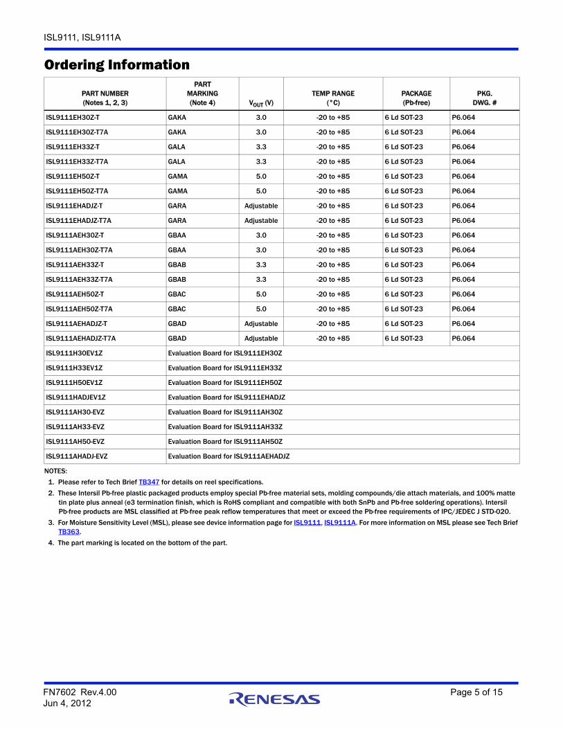
Ordering Information
PART NUMBER(Notes 1, 2, 3)
PARTMARKING(Note 4) VOUT (V)
TEMP RANGE(°C)
PACKAGE(Pb-free)
PKG. DWG. #
ISL9111EH30Z-T GAKA 3.0 -20 to +85 6 Ld SOT-23 P6.064
ISL9111EH30Z-T7A GAKA 3.0 -20 to +85 6 Ld SOT-23 P6.064
ISL9111EH33Z-T GALA 3.3 -20 to +85 6 Ld SOT-23 P6.064
ISL9111EH33Z-T7A GALA 3.3 -20 to +85 6 Ld SOT-23 P6.064
ISL9111EH50Z-T GAMA 5.0 -20 to +85 6 Ld SOT-23 P6.064
ISL9111EH50Z-T7A GAMA 5.0 -20 to +85 6 Ld SOT-23 P6.064
ISL9111EHADJZ-T GARA Adjustable -20 to +85 6 Ld SOT-23 P6.064
ISL9111EHADJZ-T7A GARA Adjustable -20 to +85 6 Ld SOT-23 P6.064
ISL9111AEH30Z-T GBAA 3.0 -20 to +85 6 Ld SOT-23 P6.064
ISL9111AEH30Z-T7A GBAA 3.0 -20 to +85 6 Ld SOT-23 P6.064
ISL9111AEH33Z-T GBAB 3.3 -20 to +85 6 Ld SOT-23 P6.064
ISL9111AEH33Z-T7A GBAB 3.3 -20 to +85 6 Ld SOT-23 P6.064
ISL9111AEH50Z-T GBAC 5.0 -20 to +85 6 Ld SOT-23 P6.064
ISL9111AEH50Z-T7A GBAC 5.0 -20 to +85 6 Ld SOT-23 P6.064
ISL9111AEHADJZ-T GBAD Adjustable -20 to +85 6 Ld SOT-23 P6.064
ISL9111AEHADJZ-T7A GBAD Adjustable -20 to +85 6 Ld SOT-23 P6.064
ISL9111H30EV1Z Evaluation Board for ISL9111EH30Z
ISL9111H33EV1Z Evaluation Board for ISL9111EH33Z
ISL9111H50EV1Z Evaluation Board for ISL9111EH50Z
ISL9111HADJEV1Z Evaluation Board for ISL9111EHADJZ
ISL9111AH30-EVZ Evaluation Board for ISL9111AH30Z
ISL9111AH33-EVZ Evaluation Board for ISL9111AH33Z
ISL9111AH50-EVZ Evaluation Board for ISL9111AH50Z
ISL9111AHADJ-EVZ Evaluation Board for ISL9111AEHADJZ
NOTES:
1. Please refer to Tech Brief TB347 for details on reel specifications.
2. These Intersil Pb-free plastic packaged products employ special Pb-free material sets, molding compounds/die attach materials, and 100% matte tin plate plus anneal (e3 termination finish, which is RoHS compliant and compatible with both SnPb and Pb-free soldering operations). Intersil Pb-free products are MSL classified at Pb-free peak reflow temperatures that meet or exceed the Pb-free requirements of IPC/JEDEC J STD-020.
3. For Moisture Sensitivity Level (MSL), please see device information page for ISL9111, ISL9111A. For more information on MSL please see Tech Brief TB363.
4. The part marking is located on the bottom of the part.
FN7602 Rev.4.00 Page 5 of 15Jun 4, 2012

ISL9111, ISL9111A
Absolute Maximum Ratings Thermal InformationVIN, EN, FAULT, VOUT . . . . . . . . . . . . . . . . . . . . . . . . . . . . . . . . . . -0.3V to 6.5VFB . . . . . . . . . . . . . . . . . . . . . . . . . . . . . . . . . . . . . . . . . . . . . . . . . -0.3V to 6.5VSW Voltage DC . . . . . . . . . . . . . . . . . . . . . . . . . . . . . . . . . . . . . . . . . . . . . . . . . -0.5V to 6.5VPulse < 10ns . . . . . . . . . . . . . . . . . . . . . . . . . . . . . . . . . . . . . . . . -0.5V to 8.0VESD Ratings
Human Body Model (Tested per JESD22-A114F) . . . . . . . . . . . . . . . . 3kVMachine Model (Tested per JESD22-A115-A) . . . . . . . . . . . . . . . . . . 250V*Other ESD Spec should meet Level 1 requirement
Latch Up (Tested per JESD78; Class 2, Level A) . . . . . . . . . . . . . . . . 100mA
Thermal Resistance (Typical) JA (°C/W)
6 Ld SOT-23 (Note 5) . . . . . . . . . . . . . . . . . . . . . . . . . . . . 146Junction Temperature Range . . . . . . . . . . . . . . . . . . . . . . .-20°C to +125°COperating Temperature Range . . . . . . . . . . . . . . . . . . . . . . . -20°C to +85°CStorage Temperature Range. . . . . . . . . . . . . . . . . . . . . . . .-65°C to +150°CPb-Free Reflow Profile . . . . . . . . . . . . . . . . . . . . . . . . . . . . . . . see link below
http://www.intersil.com/pbfree/Pb-FreeReflow.asp
Recommended Operating ConditionsVIN. . . . . . . . . . . . . . . . . . . . . . . . . . . . . . . . . . . . . . . . . . 0.8V to VOUT - 200mVAmbient Temperature Range . . . . . . . . . . . . . . . . . . . . . . . . -20°C to +85°CMaximum DC Current from Input . . . . . . . . . . . . . . . . . . . . . . . . . . . . 750mA
CAUTION: Do not operate at or near the maximum ratings listed for extended periods of time. Exposure to such conditions may adversely impact productreliability and result in failures not covered by warranty.
NOTE:5. JA is measured with the component mounted on a high effective thermal conductivity test board in free air. See Tech Brief TB379 for details.
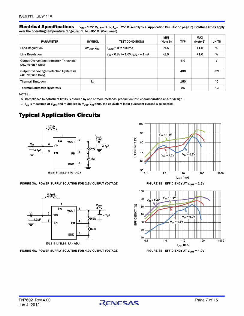
Electrical Specifications VIN = 1.2V, VOUT = 3.3V, TA = +25°C (see “Typical Application Circuits” on page 7). Boldface limits apply over the operating temperature range, -20°C to +85°C.
PARAMETER SYMBOL TEST CONDITIONSMIN
(Note 6) TYPMAX
(Note 6) UNITS
Minimum Start-up Voltage (ISL9111) VMIN VEN = VIN, RLOAD = 50Ω 0.80 0.90 V
Minimum Operating Voltage after Start-up (ISL9111)
VUVLO VEN = VIN, RLOAD = 50Ω 0.68 0.70 0.76 V
Minimum Start-up Voltage (ISL9111A) VMIN VEN = VIN, No Load 0.75 V
Minimum Operating Voltage after Start-up (ISL9111A)
VOPT VEN = VIN, No Load 0.50 V
Output Voltage Range (ISL9111-ADJ/ISL9111A-ADJ)
VOUT VIN < VOUT 2.5 5.25 V
Output Voltage Accuracy(ISL9111: 3.0/3.3/5.0V, ISL9111A: 3.0/3.3/5.0V)
VOUT VIN = 1.2V, ILOAD = 50mA -100 +100 mV
Feedback Voltage(ISL9111-ADJ/ISL9111A-ADJ)
VFB VOUT = 5V 784 800 816 mV
Feedback Pin Input Current 100 nA
Quiescent Current from VOUT IQ1 No Load (Note 7) 20 45 μA
Shutdown Current from VIN ISD VEN = 0V, VIN = 1.2V, VO = 0 0.5 2 μA
Leakage Current at SW Pin VEN = 0V, VIN = 5V, VO = 0, TA = +25°C 1 μA
N-Channel MOSFET ON-Resistance VOUT = 5V 0.2 Ω
P-Channel MOSFET ON-Resistance VOUT = 5V 0.35 Ω
N-Channel MOSFET Peak Current Limit IPK 0.8 1.0 1.2 A
Maximum Duty Cycle DMAX 84 87.5 %
PWM Switching Frequency FOSC 1.0 1.2 1.4 MHz
Soft-Start-Up Time 1 ms
EN Logic High 0.8*VIN V
EN Logic Low 0.2*VIN V
FAULT Pin Leakage Current when High VFLT = VOUT 100 nA
FAULT Pin Sink Current when Low VFLT = 0.5V 10 mA
FN7602 Rev.4.00 Page 6 of 15Jun 4, 2012
ISL9111, ISL9111A
Load Regulation ΔVOUT/VOUT ILOAD = 0 to 100mA -1.5 +1.5 %
Line Regulation VIN = 0.8V to 1.6V, ILOAD = 1mA -1.0 +1.0 %
Output Overvoltage Protection Threshold (ADJ Version Only)
5.9 V
Output Overvoltage Protection Hysteresis (ADJ Version Only)
400 mV
Thermal Shutdown TSD 150 °C
Thermal Shutdown Hysteresis 25 °C
NOTES:
6. Compliance to datasheet limits is assured by one or more methods: production test, characterization and/or design.
7. IQ1 is measured at VOUT and multiplied by VOUT/VIN; thus, the equivalent input quiescent current is calculated.
Electrical Specifications VIN = 1.2V, VOUT = 3.3V, TA = +25°C (see “Typical Application Circuits” on page 7). Boldface limits apply over the operating temperature range, -20°C to +85°C. (Continued)
PARAMETER SYMBOL TEST CONDITIONSMIN
(Note 6) TYPMAX
(Note 6) UNITS
Typical Application Circuits
FIGURE 3A. POWER SUPPLY SOLUTION FOR 2.5V OUTPUT VOLTAGE FIGURE 3B. EFFICIENCY AT VOUT = 2.5V
FIGURE 4A. POWER SUPPLY SOLUTION FOR 4.0V OUTPUT VOLTAGE FIGURE 4B. EFFICIENCY AT VOUT = 4.0V
SW
EN
GND
FB
VOUTVIN6
5
43
2
1
4.7µH
4.7µF
4.7µFVIN
VOUT
357k
166k
2.5V
ISL9111, ISL9111A - ADJ50
60
70
80
90
100
0.1 1.0 10 100 1000
IOUT (mA)
EF
FIC
IEN
CY
(%
)
VIN = 0.9VVIN = 1.2V
VIN = 1.8V
SW
EN
GND
FB
VOUTVIN6
5
43
2
1
4.7µH
4.7µF
4.7µFVIN
VOUT
665k
166k
4.0V
ISL9111, ISL9111A - ADJ
40
50
60
70
80
90
100
0.1 1.0 10 100 1000
IOUT (mA)
EF
FIC
IEN
CY
(%
)
VIN = 1.5V
VIN = 0.9V
VIN = 1.8VVIN = 2.4V
FN7602 Rev.4.00 Page 7 of 15Jun 4, 2012

ISL9111, ISL9111A
Detailed DescriptionCurrent Mode PWM OperationThe control scheme of the device is based on the peak current mode control, and the control loop is compensated internally. The peak current of the N-channel MOSFET switch is sensed to limit the maximum current flowing through the switch and the inductor. The typical current limit is set to 1A.
The control circuit includes ramp generator, slope compensator, error amplifier, PWM comparator (see block diagrams on page 2 and page 3). The ramp signal is derived from the inductor current. This ramp signal is then compared to the error amplifier output to generate the PWM gating signals for driving both N-channel and P-channel MOSFETs. The PWM operation is initialized by the clock from the internal oscillator (typical 1.2MHz). The N-channel MOSFET is turned on at the beginning of a PWM cycle, the P-channel MOSFET remains off, and the current starts ramping up. When the sum of the ramp and the slope compensator output reaches the error amplifier output voltage, the PWM comparator outputs a signal to turn off the N-channel MOSFET. Here, both MOSFETs remain off during the dead-time interval, and then the P-channel MOSFET is turned on and remains on until the end of this PWM cycle. During this time, the inductor current ramps down until the next clock. At this point, following a short dead time, the N-channel MOSFET is again turned on, repeating as previously described.
Skip Mode OperationThe device is capable of operating in two different modes. When the inductor current is sensed to cross zero for eight consecutive times, the converter enters skip mode. In skip mode, each pulse cycle is still synchronized by the PWM clock. The N-channel MOSFET is turned on at the rising edge of the clock and turned off when the inductor peak current reaches typically 25% of the current limit. Then the P-channel MOSFET is turned on, and it stays on until its current goes to zero. Subsequently, both N-channel and P-channel MOSFETs are turned off until the next clock cycle starts, at which time the N-channel MOSFET is turned on again. When VOUT is 1.5% typically higher than the nominal output voltage, the N-channel MOSFET is immediately turned off and the P-channel MOSFET is turned on until the inductor current
goes to zero. The N-channel MOSFET resumes operation when VFB falls back to its nominal value, repeating the previous operation. The converter returns to 1.2MHz PWM mode operation when VFB drops 1.5% below its nominal voltage.
Given the skip mode algorithm incorporated in the ISL9111 and ISL9111A, the average value of the output voltage is approximately 0.75% higher than the nominal output voltage under PWM operation. This positive offset improves the load transient response when switching from skip mode to PWM mode operation. The ripple on the output voltage is typically 1.5%*VOUT(nominal) when input voltage is sufficiently lower than output voltage, and it increases as input voltage approaches output voltage. Figure 9 shows the ripple voltage versus input voltage.
Synchronous RectifierThe ISL9111 and ISL9111A integrate one N-channel MOSFET and one P-channel MOSFET to realize synchronous boost converters. Because the commonly used discrete Schottky rectifier is replaced with the low rDS(ON) P-channel MOSFET, the power conversion efficiency reaches a value above 90%. Since a typical step-up converter has a conduction path from the input to the output via the body diode of the P-channel MOSFET, a special circuit (see Block Diagrams on page 2 and page 3) is used to reverse the polarity of the P-channel body diode when the part is shut down. This configuration completely disconnects the load from the input during shutdown of the converter. The benefit of this feature is that the battery will not be completely depleted during shutdown of the converter. No additional components are needed to disconnect the battery from the output of the converter.
Minimum Startup and Minimum Operating VoltageThe ISL9111 and ISL9111A address applications with rechargeable and non-rechargeable battery cells.
1. The ISL9111 has a UVLO feature. The part can start up with a 0.8V typical input voltage and internally shut off when the battery drops below 0.7V to protect a rechargeable battery from over-discharge.
FIGURE 5A. POWER SUPPLY SOLUTION FOR 5.25V OUTPUT VOLTAGE FIGURE 5B. EFFICIENCY AT VOUT = 5.25V
Typical Application Circuits (Continued)
SW
EN
GND
FB
VOUTVIN6
5
43
2
1
4.7µH
4.7µF
4.7µFVIN
VOUT
923k
166k
5.25V
ISL9111, ISL9111A - ADJ
40
50
60
70
80
90
100
0.1 1.0 10 100 1000
IOUT (mA)
EF
FIC
IEN
CY
(%
)
VIN = 1.5V
VIN = 0.9V
VIN = 1.8V
VIN = 3.6V
VIN = 4.2V
FN7602 Rev.4.00 Page 8 of 15Jun 4, 2012
ISL9111, ISL9111A
2. UVLO function is disabled in the ISL9111A. The minimum start-up voltage can be as low as 0.6V, and minimum operating voltage can be as low as 0.5V after start-up. The advantage of minimum operating voltage maximizes the performance of a non-rechargeable battery, allowing the system to operate until the battery is fully depleted.
Soft-startWhen the device is enabled, the start-up cycle starts with linear phase. During linear phase, the rectifying switch is turned on in a current limited configuration, delivering about 200mA, until the output capacitor is charged to approximately 90% of the input voltage. At this point, PWM begins, and thus, boost operation starts. If the output voltage is below 2.3V, PWM switching is done at a fixed duty-cycle of 75% until the output voltage reaches 2.3V. When the output voltage exceeds 2.3V, the closed-loop current mode PWM loop overrides the duty cycle until the output voltage is regulated. Peak inductor current is ramped to the final value (typically 1A) during the soft-start period to limit in-rush current from the input source. Fault monitoring begins approximately 2ms after the device is enabled.
Over-temperature Protection (OTP)The device offers over-temperature protection. A temperature sensor circuit is integrated and monitors the internal IC temperature. Once the temperature exceeds the preset threshold (typically +150°C), the IC shuts down immediately. The OTP has a typical hysteresis of +25°C. When the device temperature decreases by this, the device starts operating.
Overvoltage Protection (OVP) The adjustable version of the ISL9111 and ISL9111A have built in overvoltage protection (OVP) to enhance product robustness for transient up to 8V on SW pin. VOUT is actively monitored, and should the voltage reach 5.9V (typical), the device will stop switching. This turns off both power MOSFETs and the stored inductor energy is discharged to VOUT through the body diode of the synchronous rectifier.
Fault Monitoring and ReportingFault monitoring starts 2ms after start-up. Table 1 shows the response to different detected faults. Any fault condition shown in Table 1 causes the FAULT pin to be taken low. The FAULT pin will not release until VIN and VOUT fully collapse or until the fault condition is removed.
Board Layout RecommendationsThe ISL9111 and ISL9111A are high frequency switching boost converters. Accordingly, the converter creates fast voltage changes and high switching current that may cause EMI and stability issues if good PCB layout practices are not followed.
Although the ISL9111 and ISL9111A can tolerate short durations of 8.0V transients, prolonged or higher amplitude excursions may damage the device. Care should be taken to minimize the trace inductance and reduce the area of the power loop.
Power components such as input capacitor, inductor and output capacitor should be placed close to the device. Board traces that
carry high switching current should be routed wide and short. A solid power ground plane is important for EMI suppression.
The switching node (SW pin) of the converter and the traces connected to this pin are noisy. Noise sensitive traces such as the feedback trace should be kept away from SW pin and traces. The voltage divider should be placed close to the feedback pin to prevent noise pickup. Figure 6 shows the recommended EVB layout.
Fixed Output Voltage and Adjustable Output VoltageISL9111 and ISL9111A offer options for fixed output voltages of 5V, 3.3V and 3V, or an adjustable output voltage.
For fixed output voltage versions (ISL9111-5.0, ISL9111A-5.0, ISL9111-3.3, ISL9111A-3.3, ISL9111-3.0, ISL9111A-3.0), an internal voltage divider is used (see “Block Diagram: ISL9111-3.0/3.3/5.0V, ISL9111A-3.0/3.3/5.0V” on page 3). For the adjustable output voltage version (ISL9111-ADJ, ISL9111A -ADJ), the output voltage is programmed by connecting two external voltage divider resistors among OUT, FB and GND (see “Block Diagram: ISL9111-ADJ, ISL9111A-ADJ” on page 2).
Output Voltage Setting Resistor SelectionFor the ISL9111 adjustable output version, the resistors, R1 and R2, as shown in the block diagram on page 2, set the desired output voltage values. The output voltage can be calculated using Equation 1:
where VFB is the internal feedback reference voltage (0.8V typical). The current flowing through the divider resistors is calculated as VO/(R1 + R2). Large resistance is recommended to minimize current into the divider and thus improve the total efficiency of the converter. R1 and R2 should be placed close to the feedback pin of the device to prevent noise pickup.
FIGURE 6. RECOMMENDED EVALUATION BOARD LAYOUT
VIN
VOUT
GND
GND
VO VFB 1R1R2-------+
= (EQ. 1)
FN7602 Rev.4.00 Page 9 of 15Jun 4, 2012
ISL9111, ISL9111A
Inductor SelectionAn inductor with core material suitable for high frequency applications (e.g., ferrite) is desirable to minimize core loss and improve efficiency. The inductor should have a low ESR to reduce copper loss. Moreover, the inductor saturation current should be higher than the maximum peak current of the part; i.e., 1.2A.
The part is designed to operate with an inductor value of 4.7µH to provide stable operation across the range of load, input and output voltages. Stable mode switching between PWM and skip mode operation is guaranteed at this inductor value. Table 2 shows recommended inductors.
Capacitor Selection
INPUT CAPACITOR A minimum 4.7µF ceramic capacitor is recommended to provide stable operation under typical operating conditions. For input voltage less than 1.0V application, an additional 4.7µF ceramic capacitor is recommended for better noise filtering and EMI suppression. The input capacitor should be placed close to the input pin, GND pin, and the non-switching terminal of the inductor.
OUTPUT CAPACITORFor the output capacitor, a ceramic capacitor with small ESR is recommended to minimize output voltage ripple. A typical 4.7µF should be used to provide stable operation at different typical operating conditions. The output capacitor should be placed close to the output pin and GND pin of the device. Table 3 shows recommended capacitors.
TABLE 1. FAULT DETECTION AND RESPONSE
FAULT CONDITION DETECTION DETAILS ACTION
Low Battery Voltage(ISL9111 only)
VIN < 0.7V Shut down until VEN or VIN is cycled.
VOUT Out of Regulation VOUT is 10% below the target output voltage. Shut down only if VIN and VOUT fall below 2.1V. Device automatically restarts after 200ms.
Fault signal switches on and off when VOUT drops out of regulation due to overload condition.
Short Circuit VOUT falls below VIN. Shut down immediately. Device automatically restarts after 200ms.
Over-temperature Protection Die temperature is > +150°C. Switching stops. Device restarts when temperature decreases to +125°C (typical).
Output Overvoltage Protection (ADJ Version Only)
VOUT > 5.90V Switching stops until VOUT drops 400mV below OVP threshold.
TABLE 2. INDUCTOR VENDOR INFORMATION
MANUFACTURER SERIES WEBSITE
Sumida CDRH2D18/HPNP www.sumida.com
Abracon ASPI-0412FS www.abracon.com
Bourns SDR0302 www.bourns.com
Taiyo Yuden NRS4012 www.t-yuden.com
TDK VLF5012AT www.tdk.com
TABLE 3. CAPACITOR VENDOR INFORMATION
MANUFACTURER SERIES WEBSITE
AVX X5R www.avx.com
Murata X5R www.murata.com
Taiyo Yuden X5R www.t-yuden.com
TDK X5R www.tdk.com
FN7602 Rev.4.00 Page 10 of 15Jun 4, 2012

ISL9111, ISL9111A
Typical Characteristics
FIGURE 7. EFFICIENCY AT VOUT = 3.0V FIGURE 8. EFFICIENCY AT VOUT = 3.3V
FIGURE 9. OUTPUT RIPPLE vs INPUT VOLTAGE FIGURE 10. QUIESCENT CURRENT vs TEMPERATURE
FIGURE 11. MAXIMUM OUTPUT CURRENT vs INPUT VOLTAGE FIGURE 12. LINE REGULATION, VOUT = 3.3V
50
60
70
80
90
100
0.1 1 10 100 1000
IOUT (mA)
EF
FIC
IEN
CY
(%
)
VIN = 1.2VVIN = 0.9V
VIN = 1.8V
50
60
70
80
90
100
0.1 1 10 100 1000
IOUT (mA)
EF
FIC
IEN
CY
(%
)
VIN = 1.8VVIN = 1.2V
VIN = 2.4V
0
50
100
150
200
250
300
0 1 2 3 4 5
VIN (V)
VR
IPP
LE (
mV
)
5.0V_10mA
3.3V_0A
3.3V_10mA
5.0V_0A
3.0V_10mA
3.0V_0A
27.5
28.0
28.5
29.0
29.5
30.0
30.5
31.0
31.5
32.0
32.5
0 1 2 3 4 5 6
I Q (
μA
)+85°C
+25°C
VIN (V)
-40°C
-10°C
0
100
200
300
400
500
600
700
0.5 1.0 1.5 2.0 2.5 3.0 3.5 4.0 4.5 5.0 5.5VIN (V)
I OU
T (
mA
)
VO = 3.3V
VO = 5.0V
VO = 3.0V
3.320
3.325
3.330
3.335
3.340
3.345
3.350
3.355
0.6 0.8 1.0 1.2 1.4 1.6 1.8
VIN (V)
VO
UT (
V)
IOUT = 1mA(PSM)
IOUT = 50mA(PWM)
FN7602 Rev.4.00 Page 11 of 15Jun 4, 2012
ISL9111, ISL9111A
FIGURE 13. LOAD REGULATION, VIN = 1.2V FIGURE 14. LINE REGULATION, VOUT = 5.0
FIGURE 15. LOAD REGULATION, VIN = 3.6V FIGURE 16. START-UP WITH MINIMUM RESISTANCE (PRELOADED) vs VIN
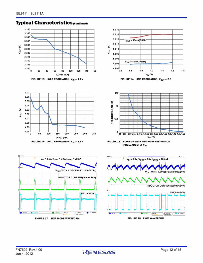
FIGURE 17. SKIP MODE WAVEFORM FIGURE 18. PWM WAVEFORM
Typical Characteristics (Continued)
3.300
3.305
3.310
3.315
3.320
3.325
3.330
3.335
3.340
3.345
3.350
0 20 40 60 80 100 120 140 160
LOAD (mA)
VO
UT (
V)
4.990
4.995
5.000
5.005
5.010
5.015
5.020
5.025
5.030
0.6 0.8 1.0 1.2 1.4 1.6 1.8
VIN (V)
VO
UT (
V)
IOUT = 10mA(PSM)
IOUT = 40mA(PWM)
4.98
4.99
5.00
5.01
5.02
5.03
5.04
5.05
5.06
5.07
0 50 100 150 200 250 300 350
LOAD (mA)
VO
UT (
V)
10
100
1k
10k
0.5 0.55 0.60 0.65 0.70 0.75 0.80 0.85 0.90 0.95 1.00 1.05 1.10 1.15 1.20 VIN (V)
RE
SIS
TO
R L
OA
D (
Ω)
VIN = 3.6V, VOUT = 5.0V, ILOAD = 20mA
VOUT WITH 5.0V OFFSET(200mV/DIV)
INDUCTOR CURRENT(200mA/DIV)
SW(2.0V/DIV)
VIN = 3.6V, VOUT = 5.0V, ILOAD = 200mA
VOUT WITH 5.0V OFFSET(50mV/DIV)
INDUCTOR CURRENT(200mA/DIV)
SW(2.0V/DIV)
FN7602 Rev.4.00 Page 12 of 15Jun 4, 2012
ISL9111, ISL9111A
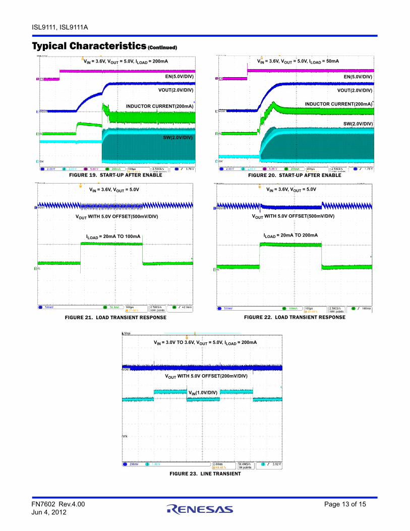
FIGURE 19. START-UP AFTER ENABLE FIGURE 20. START-UP AFTER ENABLE
FIGURE 21. LOAD TRANSIENT RESPONSE FIGURE 22. LOAD TRANSIENT RESPONSE
FIGURE 23. LINE TRANSIENT
Typical Characteristics (Continued)
VIN = 3.6V, VOUT = 5.0V, ILOAD = 200mA
VOUT(2.0V/DIV)
INDUCTOR CURRENT(200mA)
EN(5.0V/DIV)
SW(2.0V/DIV)
VIN = 3.6V, VOUT = 5.0V, ILOAD = 50mA
VOUT(2.0V/DIV)
INDUCTOR CURRENT(200mA)
EN(5.0V/DIV)
SW(2.0V/DIV)
VIN = 3.6V, VOUT = 5.0V
VOUT WITH 5.0V OFFSET(500mV/DIV)
ILOAD = 20mA TO 100mA
VIN = 3.6V, VOUT = 5.0V
ILOAD = 20mA TO 200mA
VOUT WITH 5.0V OFFSET(500mV/DIV)
VIN = 3.0V TO 3.6V, VOUT = 5.0V, ILOAD = 200mA
VOUT WITH 5.0V OFFSET(200mV/DIV)
VIN(1.0V/DIV)
FN7602 Rev.4.00 Page 13 of 15Jun 4, 2012

ISL9111, ISL9111A
Intersil products are manufactured, assembled and tested utilizing ISO9001 quality systems as notedin the quality certifications found at www.intersil.com/en/support/qualandreliability.html
Intersil products are sold by description only. Intersil may modify the circuit design and/or specifications of products at any time without notice, provided that such modification does not, in Intersil's sole judgment, affect the form, fit or function of the product. Accordingly, the reader is cautioned to verify that datasheets are current before placing orders. Information furnished by Intersil is believed to be accurate and reliable. However, no responsibility is assumed by Intersil or its subsidiaries for its use; nor for any infringements of patents or other rights of third parties which may result from its use. No license is granted by implication or otherwise under any patent or patent rights of Intersil or its subsidiaries.
For information regarding Intersil Corporation and its products, see www.intersil.com
For additional products, see www.intersil.com/en/products.html
© Copyright Intersil Americas LLC 2011-2012. All Rights Reserved.All trademarks and registered trademarks are the property of their respective owners.
About IntersilIntersil Corporation is a leading provider of innovative power management and precision analog solutions. The company's products address some of the largest markets within the industrial and infrastructure, mobile computing, and high-end consumer markets.
For the most updated datasheet, application notes, related documentation, and related parts, see the respective product information page found at www.intersil.com.
For a listing of definitions and abbreviations of common terms used in our documents, visit www.intersil.com/glossary.
You can report errors or suggestions for improving this datasheet by visiting www.intersil.com/ask.
Reliability reports are also available from our website at www.intersil.com/support.
Revision HistoryThe revision history provided is for informational purposes only and is believed to be accurate, but not warranted. Please go to web to make sure you have the latest revision.
DATE REVISION CHANGE
May 16, 2012 FN7602.4 Corrected y-axis scale on Figures 2, 7, 8 and 16.Updated evaluation board part numbers in the “Ordering Information” table on page 5.
December 7, 2011 FN7602.3 Initial release to web.
FN7602 Rev.4.00 Page 14 of 15Jun 4, 2012

ISL9111, ISL9111A
FN7602 Rev.4.00 Page 15 of 15Jun 4, 2012
Package Outline Drawing
P6.0646 LEAD SMALL OUTLINE TRANSISTOR PLASTIC PACKAGERev 4, 2/10
Dimension is exclusive of mold flash, protrusions or gate burrs.
Package conforms to JEDEC MO-178AB.
Foot length is measured at reference to guage plane.
Dimensions in ( ) for Reference Only.
Dimensioning and tolerancing conform to ASME Y14.5M-1994.
5.
3.
4.
2.
Dimensions are in millimeters.1.
NOTES:
DETAIL "X"SIDE VIEW
TYPICAL RECOMMENDED LAND PATTERN
TOP VIEW
END VIEW
INDEX AREAPIN 1
SEATING PLANE
GAUGE
0.45±0.1
(2 PLCS)10° TYP
4
1.90
0.40 ±0.10
2.90 ±0.10
0.95
1.60 +0.15/-0.102.80
0.00-0.15
1.15 +0.15/-0.25
0.20 C A-B DM
(1.20)
(0.60)
(0.95)
(2.40)
0.10 C
0.08-0.22
SEE DETAIL X
(0.25)1.45 MAX
(0.60)
0-8°
C
B
A
D
3
3
3
3
0.20 C2x
1 2 3
6 5 4
PLANE