configurable mixed-signal array with on-board...
TRANSCRIPT

May 17, 2005 Document #: 38-12010 CY Rev. *C 1
Not Recommended for New Designs: Use CY8C27xxx
Configurable
Mixed-Signal Array
with On-board Controller
CY8C25122, CY8C26233, CY8C26443, CY8C26643
Device Data Sheet for Silicon Revision D
Programmable System-on-Chip (PSoC™)
[+] Feedback
CY8C25122/CY8C26233/CY8C26443/CY8C26643 Device Family Data Sheet
Getting Started in the PSoC World!
The award winning PSoC Designer software and PSoC silicon are an integrated unit. The quickest path to understand-
ing the PSoC silicon is through the PSoC Designer software GUI. This data sheet is useful for understanding the
details of the PSOC integrated circuit, but is not a good starting point for a new PSoC developer seeking to get a gen-
eral overview of this new technology.
PSoC developers are NOT required to build their own ADCs, DACs, and other peripherals. Embedded in the PSoC
Designer software are the individual data sheets, performance graphs, and PSoC User Modules (graphically selected
code packets) for the peripherals, such as the incremental ADCs, DACs, LCD controllers, op amps, low-pass filters,
etc. With simple GUI-based selection, placement, and connection, the basic architecture of a design may be
developed within PSoC Designer software without ever writing a single line of code.
Development Kits are available from the following distributors: Digi-Key, Avnet, Arrow, and Future. The Cypress Online
Store also contains development kits, C compilers, and all accessories for PSoC development. Go to the Cypress
Online Store web site at http://www.cypress.com, click the Online Store shopping cart icon at the bottom of the web
page, and click PSoC (Programmable System-on-Chip) to view a current list of available items.
Free PSoC technical training is available for beginners and is taught by a marketing or application engineer over the
phone. PSoC training classes cover designing, debugging, advanced analog, as well as application-specific classes
covering topics such as PSoC and the LIN bus. Go to http://www.cypress.com, click on Design Support located on the
left side of the web page, and select Technical Training for more details.
Certified PSoC Consultants offer everything from technical assistance to completed PSoC designs. To contact or
become a PSoC Consultant go to http://www.cypress.com, click on Design Support located on the left side of the web
page, and select CYPros Consultants.
PSoC application engineers take pride in fast and accurate response. They can be reached with a 4-hour guaranteed
response at http://www.cypress.com/support/login.cfm.
Cypress Semiconductor2700 162nd Street SW, Building D
Lynnwood, WA 98037Phone: 425.787.4400
Fax: 425.787.4641Application Support Hotline: 425.787.4814
© Cypress Semiconductor Corporation. 2000-2005. All rights reserved. PSoC™, PSoC Designer™, and Programmable System-on-Chip™ are PSoC-related trademarks of Cypress Semiconductor Corporation. All other trademarks or registered trademarks referenced herein are property of the respec-tive corporations.
The information contained herein is subject to change without notice. Cypress Semiconductor assumes no responsibility for the use of any circuitry otherthan circuitry embodied in a Cypress Semiconductor product. Nor does it convey or imply any license under patent or other rights. Cypress Semiconductordoes not authorize its products for use as critical components in life-support systems where a malfunction or failure may reasonably be expected to resultin significant injury to the user. The inclusion of Cypress Semiconductor products in life-support systems application implies that the manufacturer assumesall risk of such use and in doing so indemnifies Cypress Semiconductor against all charges. Cypress Semiconductor products are not warranted norintended to be used for medical, life-support, life-saving, critical control or safety applications, unless pursuant to an express written agreement withCypress Semiconductor.Note the following details of the Flash code protection features on Cypress Semiconductor PSoC devices.
Cypress Semiconductor products meet the specifications contained in their particular Cypress Semiconductor Data Sheets. Cypress Semiconductorbelieves that its family of products is one of the most secure families of its kind on the market today, regardless of how they are used. There may bemethods, unknown to Cypress Semiconductor, that can breach the code protection features. Any of these methods, to our knowledge, would be dishon-est and possibly illegal. Neither Cypress Semiconductor nor any other semiconductor manufacturer can guarantee the security of their code. Code pro-tection does not mean that we are guaranteeing the product as "unbreakable." Cypress Semiconductor is willing to work with the customer who isconcerned about the integrity of their code. Code protection is constantly evolving. We at Cypress Semiconductor are committed to continuously improv-ing the code protection features of our products.
2 Document #: 38-12010 CY Rev. *C May 17, 2005
[+] Feedback
Not Recommended for New Designs: Use CY8C27xxxThe PSoC™ CY8C25122/CY8C26233/CY8C26443/CY8C26643 family of programmable sys-
tem-on-chip devices replace multiple MCU-based system components with one single-chip, con-
figurable device. A PSoC device includes configurable analog and digital peripheral blocks, a fast
CPU, Flash program memory, and SRAM data memory in a range of convenient pin-outs and
memory sizes. The driving force behind this innovative programmable system-on-chip comes
from user configurability of the analog and digital arrays: the PSoC blocks.
Programmable System-on-Chip (PSoC™) Blocks
On-chip, user configurable analog and digital peripheral blocks
PSoC blocks can be used individually or in combina-tion
12 Analog PSoC blocks provide:
Up to 11-bit Delta-Sigma ADC
Up to 8-bit Successive Approximation ADC
Up to 12-bit Incremental ADC
Up to 9-bit DAC
Programmable gain amplifier
Programmable filters
Differential comparators
8 Digital PSoC blocks provide:
Multipurpose timers: event timing, real-time clock, pulse width modulation (PWM) and PWM with deadband
CRC modules
Full-duplex UARTs
SPI™ master or slave configuration
Flexible clocking sources for analog PSoC blocks
Powerful Harvard Architecture Processor with FastMultiply/Accumulate
M8C processor instruction set
Processor speeds to 24 MHz
Register speed memory transfers
Flexible addressing modes
Bit manipulation on I/O and memory
8x8 multiply, 32-bit accumulate
Flexible On-Chip Memory
Flash program storage, 4K to 16K bytes, depending on device
50,000 erase/write cycles
256 bytes SRAM data storage
In-System Serial Programming (ISSP™)
Partial Flash updates
Flexible protection modes
EEPROM emulation in Flash, up to 2,304 bytes
Programmable Pin Configurations
Schmitt trigger TTL I/O pins
Logic output drive to 25 mA with internal pull-up or pull-down resistors, High Z, or strong driver
Interrupt on pin change
Analog output drive to 40 mA
Precision, Programmable Clocking
Internal 24/48 MHz Oscillator (+/- 2.5%, no external components)
External 32.768 kHz Crystal Oscillator (optional pre-cision source for PLL)
Internal Low Speed Oscillator for Watchdog and Sleep
Dedicated Peripherals
Watchdog and Sleep Timers
Low Voltage Detection with user-configurable threshold voltages
On-chip voltage reference
Fully Static CMOS Devices using advanced Flashtechnology
Low power at high speed
Operating voltage from 3.0 to 5.25 V
Operating voltage down to 1.0 V using on-chip switch mode voltage pump
Wide temperature range: -40 oC to + 85 oC
Complete Development Tools
Powerful integrated development environment (PSoC™ Designer)
Low-cost, in-circuit emulator and programmer
May 17, 2005 Document #: 38-12010 CY Rev. *C 3
[+] Feedback

CY8C25122/CY8C26233/CY8C26443/CY8C26643 Device Family Data Sheet
This page has intentionally been left blank.
4 Document #: 38-12010 CY Rev. *C May 17, 2005
[+] Feedback

Table of Contents
1.0 Functional Overview ......................................................................................................................141.1 Key Features ..............................................................................................................................141.2 Pin-out Descriptions ...................................................................................................................15
2.0 CPU Architecture ............................................................................................................................192.1 Introduction ................................................................................................................................192.2 CPU Registers ...........................................................................................................................202.3 Addressing Modes .....................................................................................................................212.4 Instruction Set Summary ...........................................................................................................25
3.0 Memory Organization .....................................................................................................................263.1 Flash Program Memory Organization ........................................................................................263.2 RAM Data Memory Organization ...............................................................................................26
4.0 Register Organization ....................................................................................................................264.1 Introduction ................................................................................................................................264.2 Register Bank 0 Map .................................................................................................................274.3 Register Bank 1 Map ................................................................................................................28
5.0 I/O Ports ...........................................................................................................................................295.1 Introduction ................................................................................................................................29
6.0 I/O Registers ...................................................................................................................................316.1 Port Data Registers ...................................................................................................................316.2 Port Interrupt Enable Registers .................................................................................................316.3 Port Global Select Registers .....................................................................................................32
7.0 Clocking ..........................................................................................................................................357.1 Oscillator Options .......................................................................................................................357.2 System Clocking Signals ............................................................................................................38
8.0 Interrupts .........................................................................................................................................428.1 Overview ....................................................................................................................................428.2 Interrupt Control Architecture .....................................................................................................448.3 Interrupt Vectors .........................................................................................................................448.4 Interrupt Masks ..........................................................................................................................458.5 Interrupt Vector Register ...........................................................................................................468.6 GPIO Interrupt ............................................................................................................................47
9.0 Digital PSoC Blocks .......................................................................................................................489.1 Introduction ................................................................................................................................489.2 Digital PSoC Block Bank 1 Registers .........................................................................................499.3 Digital PSoC Block Bank 0 Registers .........................................................................................549.4 Global Inputs and Outputs .........................................................................................................609.5 Available Programmed Digital Functionality ...............................................................................60
10.0 Analog PSoC Blocks ....................................................................................................................7110.1 Introduction ..............................................................................................................................7110.2 Analog System Clocking Signals .............................................................................................7210.3 Array of Analog PSoC Blocks .................................................................................................7210.4 Analog Reference Control ........................................................................................................7310.5 Analog PSoC Block Clocking Options ......................................................................................7610.6 Analog Clock Select Register ..................................................................................................7710.7 Analog Continuous Time PSoC Blocks ....................................................................................80
May 17, 2005 Document #: 38-12010 CY Rev. *C 5
[+] Feedback
CY8C25122/CY8C26233/CY8C26443/CY8C26643 Device Family Data Sheet
10.8 Analog Switch Cap Type A PSoC Blocks ................................................................................8510.9 Analog Switch Cap Type B PSoC Blocks ................................................................................9410.10 Analog Comparator Bus .......................................................................................................10110.11 Analog Synchronization .......................................................................................................10110.12 Analog I/O ............................................................................................................................10310.13 Analog Modulator .................................................................................................................10610.14 Analog PSoC Block Functionality .........................................................................................10710.15 Temperature Sensing Capability ..........................................................................................108
11.0 Special Features of the CPU ......................................................................................................10911.1 Multiplier/Accumulator ............................................................................................................10911.2 Decimator ...............................................................................................................................11211.3 Reset ......................................................................................................................................11411.4 Sleep States ...........................................................................................................................11611.5 Supply Voltage Monitor ..........................................................................................................11811.6 Switch Mode Pump ................................................................................................................11911.7 Internal Voltage Reference ....................................................................................................12011.8 Supervisor ROM/System Supervisor Call Instruction .............................................................12011.9 Flash Program Memory Protection ........................................................................................12211.10 Programming Requirements and Step Descriptions ............................................................12211.11 Programming Wave Forms .................................................................................................12411.12 Programming File Format ....................................................................................................124
12.0 Development Tools ...................................................................................................................12512.1 Overview ................................................................................................................................12512.2 Integrated Development Environment Subsystems ...............................................................12612.3 Hardware Tools ......................................................................................................................126
13.0 DC and AC Characteristics ........................................................................................................12713.1 Absolute Maximum Ratings ..................................................................................................12713.2 DC Characteristics .................................................................................................................12913.3 AC Characteristics .................................................................................................................138
14.0 Packaging Information ..............................................................................................................14314.1 Thermal Impedances per Package .......................................................................................148
15.0 Ordering Guide ..........................................................................................................................14916.0 Document Revision History .......................................................................................................150
6 Document #: 38-12010 CY Rev. *C May 17, 2005
[+] Feedback

List of Tables
Table 1: Device Family Key Features.........................................................................................................14Table 2: Pin-out 8 Pin .................................................................................................................................15Table 3: Pin-out 20 Pin ...............................................................................................................................15Table 4: Pin-out 28 Pin ...............................................................................................................................16Table 5: Pin-out 44 Pin ...............................................................................................................................16Table 6: Pin-out 48 Pin ...............................................................................................................................17Table 7: CPU Registers and Mnemonics ...................................................................................................19Table 8: Flags Register ..............................................................................................................................20Table 9: Accumulator Register (CPU_A)....................................................................................................20Table 10: Index Register (CPU_X) .............................................................................................................21Table 11: Stack Pointer Register (CPU_SP) ..............................................................................................21Table 12: Program Counter Register (CPU_PC)........................................................................................21Table 13: Source Immediate ......................................................................................................................21Table 14: Source Direct..............................................................................................................................22Table 15: Source Indexed ..........................................................................................................................22Table 16: Destination Direct .......................................................................................................................22Table 17: Destination Indexed....................................................................................................................23Table 18: Destination Direct Immediate .....................................................................................................23Table 19: Destination Indexed Immediate ..................................................................................................23Table 20: Destination Direct Direct.............................................................................................................24Table 21: Source Indirect Post Increment ..................................................................................................24Table 22: Destination Indirect Post Increment............................................................................................24Table 23: Instruction Set Summary (Sorted by Mnemonic)........................................................................25Table 24: Flash Program Memory Map ......................................................................................................26Table 25: RAM Data Memory Map .............................................................................................................26Table 26: Bank 0 ........................................................................................................................................27Table 27: Bank 1 ........................................................................................................................................28Table 28: Port Data Registers ....................................................................................................................31Table 29: Port Interrupt Enable Registers ..................................................................................................31Table 30: Port Global Select Registers ......................................................................................................32Table 31: Port Drive Mode 0 Registers ......................................................................................................32Table 32: Port Drive Mode 1 Registers ......................................................................................................33Table 33: Port Interrupt Control 0 Registers...............................................................................................33Table 34: Port Interrupt Control 1 Registers...............................................................................................34Table 35: Internal Main Oscillator Trim Register ........................................................................................35Table 36: Internal Low Speed Oscillator Trim Register ..............................................................................36Table 37: External Crystal Oscillator Trim Register....................................................................................37Table 38: Typical Package Capacitances ..................................................................................................37Table 39: System Clocking Signals and Definitions ...................................................................................38Table 40: Oscillator Control 0 Register.......................................................................................................40Table 41: Oscillator Control 1 Register.......................................................................................................40Table 42: 24V1/24V2 Frequency Selection ................................................................................................41Table 43: Interrupt Vector Table.................................................................................................................44Table 44: General Interrupt Mask Register ................................................................................................45Table 45: Digital PSoC Block Interrupt Mask Register ...............................................................................46
May 17, 2005 Document #: 38-12010 CY Rev. *C 7
[+] Feedback

CY8C25122/CY8C26233/CY8C26443/CY8C26643 Device Family Data Sheet
Table 46: Interrupt Vector Register ............................................................................................................46Table 47: Digital Basic Type A/ Communications Type A Block xx Function Register...............................50Table 48: Digital Basic Type A / Communications Type A Block xx Input Register ...................................51Table 49: Digital Function Data Input Definitions .......................................................................................52Table 50: Digital Basic Type A / Communications Type A Block xx Output Register.................................53Table 51: Digital Function Outputs .............................................................................................................54Table 52: Digital Basic Type A / Communications Type A Block xx Data Register 0,1,2...........................54Table 53: R/W Variations per User Module Selection ................................................................................55Table 54: Digital Basic Type A / Communications Type A Block xx Control Register 0.............................55Table 55: Digital Basic Type A/Communications Type A Block xx Control Register 0... ............................56Table 56: Digital Communications Type A Block xx Control Register 0... ..................................................57Table 57: Digital Communications Type A Block xx Control Register 0... ..................................................58Table 58: Digital Communications Type A Block xx Control Register 0... ..................................................59Table 59: Global Input Assignments...........................................................................................................60Table 60: Global Output Assignments........................................................................................................60Table 61: Analog System Clocking Signals................................................................................................72Table 62: AGND, RefHI, RefLO Operating Parameters .............................................................................74Table 63: Analog Reference Control Register............................................................................................75Table 64: Analog Column Clock Select Register........................................................................................76Table 65: Analog Clock Select Register .....................................................................................................77Table 66: Analog Continuous Time Block xx Control 0 Register................................................................82Table 67: Analog Continuous Time Block xx Control 1 Register................................................................83Table 68: Analog Continuous Time Type A Block xx Control 2 Register ...................................................84Table 69: Analog Switch Cap Type A Block xx Control 0 Register ............................................................88Table 70: Analog Switch Cap Type A Block xx Control 1 Register ............................................................90Table 71: Analog Switch Cap Type A Block xx Control 2 Register ............................................................92Table 72: Analog Switch Cap Type A Block xx Control 3 Register ............................................................93Table 73: Analog Switch Cap Type B Block xx Control 0 Register ............................................................95Table 74: Analog Switch Cap Type B Block xx Control 1 Register ............................................................97Table 75: Analog Switch Cap Type B Block xx Control 2 Register ............................................................99Table 76: Analog Switch Cap Type B Block xx Control 3 Register ..........................................................100Table 77: Analog Comparator Control Register .......................................................................................101Table 78: Analog Frequency Relationships..............................................................................................102Table 79: Analog Synchronization Control Register.................................................................................102Table 80: Analog Input Select Register ....................................................................................................104Table 81: Analog Output Buffer Control Register .....................................................................................106Table 82: Analog Modulator Control Register ..........................................................................................107Table 83: Multiply Input X Register...........................................................................................................110Table 84: Multiply Input Y Register...........................................................................................................110Table 85: Multiply Result High Register ...................................................................................................111Table 86: Multiply Result Low Register ....................................................................................................111Table 87: Accumulator Result 1 / Multiply/Accumulator Input X Register ................................................111Table 88: Accumulator Result 0 / Multiply/Accumulator Input Y Register ................................................111Table 89: Accumulator Result 3 / Multiply/Accumulator Clear 0 Register ................................................112Table 90: Accumulator Result 2 / Multiply/Accumulator Clear 1 Register ................................................112Table 91: Decimator/Incremental Control Register ..................................................................................113Table 92: Decimator Data High Register..................................................................................................113Table 93: Decimator Data Low Register...................................................................................................113Table 94: Processor Status and Control Register ....................................................................................114Table 95: Reset WDT Register.................................................................................................................116Table 96: Voltage Monitor Control Register .............................................................................................118Table 97: Bandgap Trim Register.............................................................................................................120Table 98: CY8C25122, CY8C26233, CY8C26443, CY8C26643 (256 Bytes of SRAM) ..........................121Table 99: Table Read for Supervisory Call Functions ..............................................................................122
8 Document #: 38-12010 CY Rev. *C May 17, 2005
[+] Feedback

Table 100: Flash Program Memory Protection.........................................................................................122Table 101: Programmer Requirements ....................................................................................................122Table 102: Absolute Maximum Ratings....................................................................................................127Table 103: Temperature Specifications....................................................................................................128Table 104: DC Operating Specifications ..................................................................................................129Table 105: 5V DC Operational Amplifier Specifications ...........................................................................130Table 106: 3.3V DC Operational Amplifier Specifications ........................................................................131Table 107: DC Analog Input Pin with Multiplexer Specifications ..............................................................132Table 108: DC Analog Input Pin to SC Block Specifications ....................................................................132Table 109: 5V DC Analog Output Buffer Specifications ...........................................................................132Table 110: 3.3V DC Analog Output Buffer Specifications ........................................................................133Table 111: DC Switch Mode Pump Specifications ...................................................................................134Table 112: 5V DC Analog Reference Specifications ................................................................................135Table 113: 3.3V DC Analog Reference Specifications .............................................................................136Table 114: DC Analog PSoC Block Specifications...................................................................................136Table 115: DC Programming Specifications.............................................................................................137Table 116: AC Operating Specifications...................................................................................................138Table 117: 5V AC Operational Amplifier Specifications ...........................................................................139Table 118: 3.3V AC Operational Amplifier Specifications ........................................................................140Table 119: 5V AC Analog Output Buffer Specifications ...........................................................................141Table 120: 3.3V AC Analog Output Buffer Specifications ........................................................................142Table 121: AC Programming Specifications.............................................................................................142Table 122: Thermal Impedances..............................................................................................................148Table 123: Ordering Guide (Leaded)........................................................................................................149Table 124: Ordering Guide (Pb-Free Denoted with an “X” in Ordering Code) .........................................149Table 125: Document Revision History ....................................................................................................150
May 17, 2005 Document #: 38-12010 CY Rev. *C 9
[+] Feedback

CY8C25122/CY8C26233/CY8C26443/CY8C26643 Device Family Data Sheet
10 Document #: 38-12010 CY Rev. *C May 17, 2005
[+] Feedback

List of Figures
Figure 1: Block Diagram ............................................................................................................................13Figure 2: CY8C25122 ................................................................................................................................15Figure 3: CY8C26233 ................................................................................................................................15Figure 4: 26443 PDIP/SOIC/SSOP ...........................................................................................................16Figure 5: 26643 TQFP ...............................................................................................................................17Figure 6: 26643 PDIP/SSOP .....................................................................................................................18Figure 7: General Purpose I/O Pins ..........................................................................................................30Figure 8: External Crystal Oscillator Connections .....................................................................................37Figure 9: PSoC MCU Clock Tree of Signals ..............................................................................................39Figure 10: Interrupts Overview ..................................................................................................................43Figure 11: GPIO Interrupt Enable Diagram ...............................................................................................47Figure 12: Digital Basic and Digital Communications PSoC Blocks ..........................................................49Figure 13: Polynomial LFSR ......................................................................................................................65Figure 14: Polynomial PRS .......................................................................................................................65Figure 15: SPI Waveforms ........................................................................................................................68Figure 16: Array of Analog PSoC Blocks ...................................................................................................72Figure 17: Analog Reference Control Schematic ......................................................................................73Figure 18: NMux Connections ...................................................................................................................78Figure 19: PMux Connections ...................................................................................................................79Figure 20: RBotMux Connections ..............................................................................................................79Figure 21: Analog Continuous Time PSoC Blocks ....................................................................................81Figure 22: Analog Switch Cap Type A PSoC Blocks .................................................................................86Figure 23: AMux Connections ...................................................................................................................87Figure 24: CMux Connections ...................................................................................................................87Figure 25: BMuxSCA/SCB Connections ...................................................................................................88Figure 26: Analog Switch Cap Type B PSoC Blocks .................................................................................95Figure 27: Analog Input Muxing ...............................................................................................................103Figure 28: Analog Output Buffers ............................................................................................................105Figure 29: Multiply/Accumulate Block Diagram .......................................................................................110Figure 30: Decimator Coefficients ...........................................................................................................112Figure 31: Execution Reset .....................................................................................................................115Figure 32: Three Sleep States .................................................................................................................117Figure 33: Switch Mode Pump ................................................................................................................119Figure 34: Programming Wave Forms ....................................................................................................124Figure 35: PSoC Designer Functional Flow ............................................................................................125Figure 36: CY8C25xxx/CY8C26xxx Voltage Frequency Graph ..............................................................127Figure 37: 44-Lead Thin Plastic Quad Flat Pack A44 .............................................................................143Figure 38: 20-Pin Shrunk Small Outline Package O20 ...........................................................................144Figure 39: 28-Lead (210-Mil) Shrunk Small Outline Package O28 .........................................................145Figure 40: 48-Lead Shrunk Small Outline Package O48 .........................................................................145Figure 41: 20-Lead (300-Mil) Molded DIP P5 ..........................................................................................146Figure 42: 28-Lead (300-Mil) Molded DIP P21 ........................................................................................146Figure 43: 48-Lead (600-Mil) Molded DIP P25 ........................................................................................147Figure 44: 20-Lead (300-Mil) Molded SOIC S5 .......................................................................................147Figure 45: 28-Lead (300-Mil) Molded SOIC S21 .....................................................................................148
May 17, 2005 Document #: 38-12010 CY Rev. *C 11
[+] Feedback

CY8C25122/CY8C26233/CY8C26443/CY8C26643 Device Family Data Sheet
Figure 46: 8-Lead (300-Mil) Molded DIP .................................................................................................148
12 Document #: 38-12010 CY Rev. *C May 17, 2005
[+] Feedback
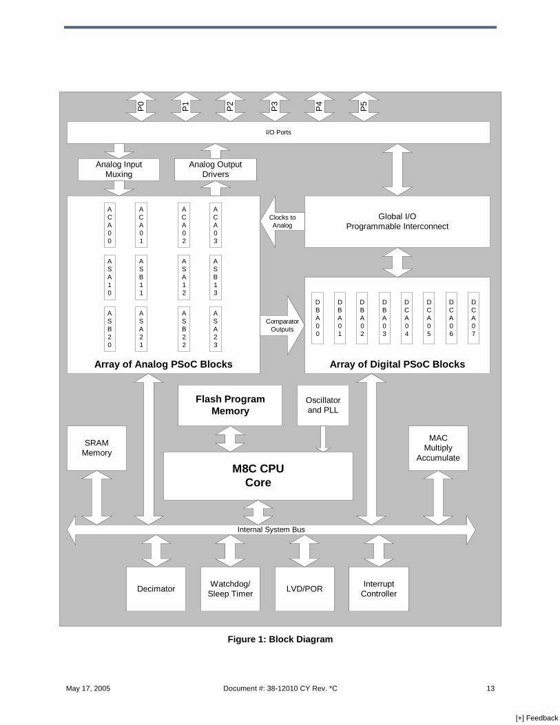
Figure 1: Block Diagram
Array of Analog PSoC Blocks
SRAMMemory
I/O Ports
Global I/OProgrammable Interconnect
Array of Digital PSoC Blocks
Analog InputMuxing
DBA00
ACA00
DBA03
DBA02
DBA01
DCA04
DCA07
DCA06
DCA05
Analog OutputDrivers
P1
P0
ComparatorOutputs
Clocks toAnalog
P3
P2
P4
P5
ASA10
ASB20
ACA01
ASB11
ASA21
ACA02
ASA12
ASB22
ACA03
ASB13
ASA23
Internal System Bus
M8C CPUCore
Flash ProgramMemory
MACMultiply
Accumulate
DecimatorWatchdog/
Sleep TimerLVD/POR
InterruptController
Oscillatorand PLL
May 17, 2005 Document #: 38-12010 CY Rev. *C 13
[+] Feedback

CY8C25122/CY8C26233/CY8C26443/CY8C26643 Device Family Data Sheet
1.0 Functional OverviewThe CPU heart of this next generation family of micro-controllers is a high performance, 8-bit, M8C Harvardarchitecture microprocessor. Separate program andmemory busses allow for faster overall throughput. Pro-cessor clock speeds to 24 MHz are available. The pro-cessor may also be run at lower clock speeds for power-sensitive applications. A rich instruction set allows forefficient low-level language support.
All devices in this family include both analog and digitalconfigurable peripherals (PSoC blocks). These blocksenable the user to define unique functions during config-uration of the device. Included are twelve analog PSoCblocks and eight digital PSoC blocks. Potential applica-tions for the digital PSoC blocks are timers, counters,UARTs, CRC generators, PWMs, and other functions.The analog PSoC blocks can be used for SAR ADCs,Multi-slope ADCs, programmable gain amplifiers, pro-grammable filters, DACs, and other functions. Higherorder User Modules such as modems, complex motorcontrollers, and complete sensor signal chains can becreated from these building blocks. This allows for anunprecedented level of flexibility and integration in micro-controller-based systems.
A Multiplier/Accumulator (MAC) is available on alldevices in this family. The MAC is implemented on thisdevice as a peripheral that is mapped into the registerspace. When an instruction writes to the MAC input reg-isters, the result of an 8x8 multiply and a 32-bit accumu-late are available to be read from the output registers onthe next instruction cycle.
The number of general purpose I/Os available in thisfamily of parts range from 6 to 44. Each of these I/O pinshas a variety of programmable options. In the output
mode, the user can select the drive strength desired.Any pin can serve as an interrupt source, and can beselected to trigger on positive edges, negative edges, orany change. Digital signal sources can be routed directlyfrom a pin to the digital PSoC blocks. Some pins haveadditional capability to route analog signals to the analogPSoC blocks.
Multiple oscillator options are available for use in clock-ing the CPU, analog PSoC blocks and digital PSoCblocks. These options include an internal main oscillatorrunning at 48/24 MHz, an external crystal oscillator foruse with a 32.768 kHz watch crystal, and an internal low-speed oscillator for use in clocking the PSoC blocks andthe Watchdog/Sleep timer. User selectable clock divisorsallow for optimizing code execution speed and powertrade-offs.
The different device types in this family provide variousamounts of code and data memory. The code spaceranges in size from 4K to 16K bytes of user programma-ble Flash memory. This memory can be programmedserially in either a programming Pod or on the userboard. The endurance on the Flash memory is 50,000erase/write cycles. The data space is 256 bytes of userSRAM.
A powerful and flexible protection model secures theuser’s sensitive information. This model allows the userto selectively lock blocks of memory for read and writeprotection. This allows partial code updates withoutexposing proprietary information.
Devices in this family range from 8 pins through 48 pinsin PDIP, SOIC and SSOP packages.
1.1 Key Features
Table 1: Device Family Key Features
CY8C25122 CY8C26233 CY8C26443 CY8C26643Operating Frequency 93.7kHz - 24MHz 93.7kHz - 24MHz 93.7kHz - 24MHz 93.7kHz - 24MHzOperating Voltage 3.0 - 5.25V 3.0 - 5.25V 3.0 - 5.25V 3.0 - 5.25VProgram Memory (KBytes) 4 8 16 16Data Memory (Bytes) 256 256 256 256Digital PSoC Blocks 8 8 8 8Analog PSoC Blocks 12 12 12 12I/O Pins 6 16 24 40/44External Switch Mode Pump No Yes Yes YesAvailable Packages 8 PDIP 20 PDIP 28 PDIP 48 PDIP
20 SOIC 28 SOIC 48 SSOP20 SSOP 28 SSOP 44 TQFP
14 Document #: 38-12010 CY Rev. *C May 17, 2005
[+] Feedback

Functional Overview
1.2 Pin-out Descriptions
Table 2: Pin-out 8 Pin
Name I/O Pin Description
P0[7] I/O 1 Port 0[7] (Analog Input)
P0[5] I/O 2 Port 0[5] (Analog Input/Output)
P1[1] I/O 3 Port 1[1] / XtalIn / SCLK
Vss Power 4 Ground
P1[0] I/O 5 Port 1[0] / XtalOut / SDATA
P0[2] I/O 6 Port 0[2] (Analog Input/Output)
P0[4] I/O 7 Port 0[4] (Analog Input/Output)
Vcc Power 8 Supply Voltage
Figure 2: CY8C25122
1234
8765
P0[7]P0[5]
XtalIn/SCLK/P1[1]P0[4]P0[2]P1[0]/XtalOut/SDATA
CY
8C25122Vss
Vcc
Table 3: Pin-out 20 Pin
Name I/O Pin Description
P0[7] I/O 1 Port 0[7] (Analog Input)
P0[5] I/O 2 Port 0[5] (Analog Input/Output)
P0[3] I/O 3 Port 0[3] (Analog Input/Output)
P0[1] I/O 4 Port 0[1] (Analog Input)
SMP O 5 Switch Mode Pump
P1[7] I/O 6 Port 1[7]
P1[5] I/O 7 Port 1[5]
P1[3] I/O 8 Port 1[3]
P1[1] I/O 9 Port 1[1] / XtalIn / SCLK
Vss Power 10 Ground
P1[0] I/O 11 Port 1[0] / XtalOut / SDATA
P1[2] I/O 12 Port 1[2]
P1[4] I/O 13 Port 1[4]
P1[6] I/O 14 Port 1[6]
XRES I 15 External Reset
P0[0] I/O 16 Port 0[0] (Analog Input)
P0[2] I/O 17 Port 0[2] (Analog Input/Output)
P0[4] I/O 18 Port 0[4] (Analog Input/Output)
P0[6] I/O 19 Port 0[6] (Analog Input)
Vcc Power 20 Supply Voltage
Figure 3: CY8C26233
12345678910
20191817161514131211
P0[7]P0[5]P0[3]P0[1]SMPP1[7]P1[5]P1[3]
XtalIn/SCLK/P1[1]
P0[6]P0[4]P0[2]P0[0]
P1[6]P1[4]P1[2]P1[0]/XtalOut/SDATA
CY
8C26233
PD
IP/S
OIC
/SS
OPVss
Vcc
XRES
May 17, 2005 Document #: 38-12010 CY Rev. *C 15
[+] Feedback
CY8C25122/CY8C26233/CY8C26443/CY8C26643 Device Family Data Sheet
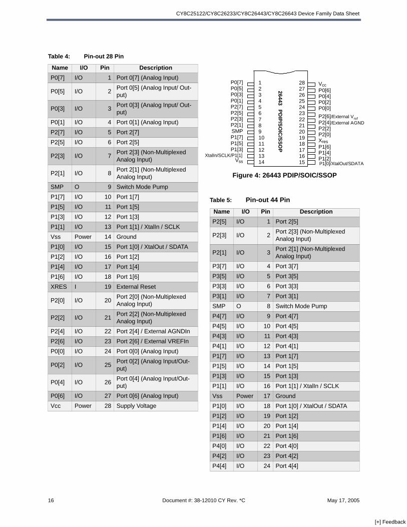
Table 4: Pin-out 28 Pin
Name I/O Pin Description
P0[7] I/O 1 Port 0[7] (Analog Input)
P0[5] I/O 2Port 0[5] (Analog Input/ Out-put)
P0[3] I/O 3Port 0[3] (Analog Input/ Out-put)
P0[1] I/O 4 Port 0[1] (Analog Input)
P2[7] I/O 5 Port 2[7]
P2[5] I/O 6 Port 2[5]
P2[3] I/O 7Port 2[3] (Non-Multiplexed Analog Input)
P2[1] I/O 8Port 2[1] (Non-Multiplexed Analog Input)
SMP O 9 Switch Mode Pump
P1[7] I/O 10 Port 1[7]
P1[5] I/O 11 Port 1[5]
P1[3] I/O 12 Port 1[3]
P1[1] I/O 13 Port 1[1] / XtalIn / SCLK
Vss Power 14 Ground
P1[0] I/O 15 Port 1[0] / XtalOut / SDATA
P1[2] I/O 16 Port 1[2]
P1[4] I/O 17 Port 1[4]
P1[6] I/O 18 Port 1[6]
XRES I 19 External Reset
P2[0] I/O 20Port 2[0] (Non-Multiplexed Analog Input)
P2[2] I/O 21Port 2[2] (Non-Multiplexed Analog Input)
P2[4] I/O 22 Port 2[4] / External AGNDIn
P2[6] I/O 23 Port 2[6] / External VREFIn
P0[0] I/O 24 Port 0[0] (Analog Input)
P0[2] I/O 25Port 0[2] (Analog Input/Out-put)
P0[4] I/O 26Port 0[4] (Analog Input/Out-put)
P0[6] I/O 27 Port 0[6] (Analog Input)
Vcc Power 28 Supply Voltage
Figure 4: 26443 PDIP/SOIC/SSOP
Table 5: Pin-out 44 Pin
Name I/O Pin Description
P2[5] I/O 1 Port 2[5]
P2[3] I/O 2Port 2[3] (Non-Multiplexed Analog Input)
P2[1] I/O 3Port 2[1] (Non-Multiplexed Analog Input)
P3[7] I/O 4 Port 3[7]
P3[5] I/O 5 Port 3[5]
P3[3] I/O 6 Port 3[3]
P3[1] I/O 7 Port 3[1]
SMP O 8 Switch Mode Pump
P4[7] I/O 9 Port 4[7]
P4[5] I/O 10 Port 4[5]
P4[3] I/O 11 Port 4[3]
P4[1] I/O 12 Port 4[1]
P1[7] I/O 13 Port 1[7]
P1[5] I/O 14 Port 1[5]
P1[3] I/O 15 Port 1[3]
P1[1] I/O 16 Port 1[1] / XtalIn / SCLK
Vss Power 17 Ground
P1[0] I/O 18 Port 1[0] / XtalOut / SDATA
P1[2] I/O 19 Port 1[2]
P1[4] I/O 20 Port 1[4]
P1[6] I/O 21 Port 1[6]
P4[0] I/O 22 Port 4[0]
P4[2] I/O 23 Port 4[2]
P4[4] I/O 24 Port 4[4]
1234567891011121314
2827262524232221201918171615
P0[7]P0[5]P0[3]P0[1]P2[7]P2[5]P2[3]P2[1]SMPP1[7]P1[5]P1[3]
XtalIn/SCLK/P1[1]
P0[6]P0[4]P0[2]P0[0]
P2[2]P2[0]
P1[6]P1[4]P1[2]P1[0]/XtalOut/SDATA
26443P
DIP
/SO
IC/S
SO
P
Xres
P2[6]/External Vref
Vcc
P2[4]/External AGND
Vss
16 Document #: 38-12010 CY Rev. *C May 17, 2005
[+] Feedback

Functional Overview
P4[6] I/O 25 Port 4[6]
XRES I 26 External Reset
P3[0] I/O 27 Port 3[0]
P3[2] I/O 28 Port 3[2]
P3[4] I/O 29 Port 3[4]
P3[6] I/O 30 Port 3[6]
P2[0] I/O 31Port 2[0] (Non-Multiplexed Analog Input)
P2[2] I/O 32Port 2[2] (Non-Multiplexed Analog Input)
P2[4] I/O 33 Port 2[4] / External AGNDIn
P2[6] I/O 34 Port 2[6] / External VREFIn
P0[0] I/O 35 Port 0[0] (Analog Input)
P0[2] I/O 36 Port 0[2] (Analog Input/Output)
P0[4] I/O 37 Port 0[4] (Analog Input/Output)
P0[6] I/O 38 Port 0[6] (Analog Input)
Vcc Power 39 Supply Voltage
P0[7] I/O 40 Port 0[7] (Analog Input)
P0[5] I/O 41 Port 0[5] (Analog Input/Output)
P0[3] I/O 42 Port 0[3] (Analog Input/Output)
P0[1] I/O 43 Port 0[1] (Analog Input)
P2[7] I/O 44 Port 2[7]
Figure 5: 26643 TQFP
Table 5: Pin-out 44 Pin, continued
1234567891011
3332313029282726252423
12 13 14 15 16 17 18 19 20 21 22
44 43 42 41 40 39 38 37 36 35 34P2[5]P2[3]P2[1]P3[7]P3[5]P3[3]P3[1]SMPP4[7]P4[5]P4[3]
P2[4]/Ex AGNDIn
P2[0]P3[6]P3[4]P3[2]P3[0]
P4[6]P4[4]P4[2]
P4[
1]P
1[7]
P1[
5]P
1[3]
Xta
lIn/S
CLK
/P1[
1]
Xta
lOut
/SD
AT
A/P
1[0]
P1[
2]P
1[4]
P1[
6]P
4[0]
P2[
7]P
0[1]
P0[
3]P
0[5]
P0[
7]
P0[
6]P
0[4]
P0[
2]P
0[0]
26643 TQF
P Xres
Vss
P2[2]
P2[
6]/E
xVre
fIn
Vcc
Table 6: Pin-out 48 Pin
Name I/O Pin Description
P0[7] I/O 1 Port 0[7] (Analog Input)
P0[5] I/O 2Port 0[5] (Analog Input/Out-put)
P0[3] I/O 3Port 0[3] (Analog Input/Out-put)
P0[1] I/O 4 Port 0[1] (Analog Input)
P2[7] I/O 5 Port 2[7]
P2[5] I/O 6 Port 2[5]
P2[3] I/O 7Port 2[3] (Non-Multiplexed Analog Input)
P2[1] I/O 8Port 2[1] (Non-Multiplexed Analog Input)
P3[7] I/O 9 Port 3[7]
P3[5] I/O 10 Port 3[5]
P3[3] I/O 11 Port 3[3]
P3[1] I/O 12 Port 3[1]
SMP O 13 Switch Mode Pump
P4[7] I/O 14 Port 4[7]
P4[5] I/O 15 Port 4[5]
P4[3] I/O 16 Port 4[3]
P4[1] I/O 17 Port 4[1]
P5[3] I/O 18 Port 5[3]
P5[1] I/O 19 Port 5[1]
P1[7] I/O 20 Port 1[7]
P1[5] I/O 21 Port 1[5]
P1[3] I/O 22 Port 1[3]
P1[1] I/O 23 Port 1[1] / XtalIn / SCLK
Vss Power 24 Ground
P1[0] I/O 25 Port 1[0] / XtalOut / SDATA
P1[2] I/O 26 Port 1[2]
P1[4] I/O 27 Port 1[4]
P1[6] I/O 28 Port 1[6]
May 17, 2005 Document #: 38-12010 CY Rev. *C 17
[+] Feedback

CY8C25122/CY8C26233/CY8C26443/CY8C26643 Device Family Data Sheet
P5[0] I/O 29 Port 5[0]
P5[2] I/O 30 Port 5[2]
P4[0] I/O 31 Port 4[0]
P4[2] I/O 32 Port 4[2]
P4[4] I/O 33 Port 4[4]
P4[6] I/O 34 Port 4[6]
XRES I 35 External Reset
P3[0] I/O 36 Port 3[0]
P3[2] I/O 37 Port 3[2]
P3[4] I/O 38 Port 3[4]
P3[6] I/O 39 Port 3[6]
P2[0] I/O 40Port 2[0] (Non-Multiplexed Analog Input)
P2[2] I/O 41Port 2[2] (Non-Multiplexed Analog Input)
P2[4] I/O 42 Port 2[4] / External AGNDIn
P2[6] I/O 43 Port 2[6] / External VREFIn
P0[0] I/O 44 Port 0[0] (Analog Input)
P0[2] I/O 45Port 0[2] (Analog Input/Out-put)
P0[4] I/O 46Port 0[4] (Analog Input/Out-put)
P0[6] I/O 47 Port 0[6] (Analog Input)
Vcc Power 48 Supply Voltage
Figure 6: 26643 PDIP/SSOP
Table 6: Pin-out 48 Pin, continued
123456789101112131415161718192021222324
484746454443424140393837363534333231302928272625
P0[7]P0[5]P0[3]P0[1]P2[7]P2[5]P2[3]P2[1]P3[7]P3[5]P3[3]P3[1]SMPP4[7]P4[5]P4[3]P4[1]P5[3]P5[1]P1[7]P1[5]P1[3]
XtalIn/SCLK/P1[1]
VccP0[6]P0[4]P0[2]P0[0]P2[6]/External Vref
P2[4] /External AGNDINP2[2]P2[0]P3[6]P3[4]P3[2]P3[0]
P4[6]P4[4]P4[2]P4[0]P5[2]P5[0]P1[6]P1[4]P1[2]P1[0]/XtalOut/SDATA
26643P
DIP
/SS
OP
Vss
Xres
IN
18 Document #: 38-12010 CY Rev. *C May 17, 2005
[+] Feedback
CPU Architecture
2.0 CPU Architecture
2.1 Introduction
This family of microcontrollers is based on a high perfor-
mance, 8-bit, Harvard architecture microprocessor. Five
registers control the primary operation of the CPU core.
These registers are affected by various instructions, but
are not directly accessible through the register space by
the user. For more details on addressing with the register
space, see section 4.0.
The 16 bit Program Counter Register (CPU_PC) allows
for direct addressing of the full 16 Kbytes of program
memory space available in the largest members of this
family. This forms one contiguous program space, and
no paging is required.
The Accumulator Register (CPU_A) is the general-pur-
pose register that holds the results of instructions that
specify any of the source addressing modes.
The Index Register (CPU_X) holds an offset value that is
used in the indexed addressing modes. Typically, this is
used to address a block of data within the data memory
space.
The Stack Pointer Register (CPU_SP) holds the address
of the current top-of-stack in the data memory space. It is
affected by the PUSH, POP, LCALL, CALL, RETI, and
RET instructions, which manage the software stack. It
can also be affected by the SWAP and ADD instructions.
The Flag Register (CPU_F) has three status bits: Zero
Flag bit [1]; Carry Flag bit [2]; Supervisory State bit [3].
The Global Interrupt Enable bit [0] is used to globally
enable or disable interrupts. An extended I/O space
address, bit [4], is used to determine which bank of the
register space is in use. The user cannot manipulate the
Supervisory State status bit [3]. The flags are affected by
arithmetic, logic, and shift operations. The manner in
which each flag is changed is dependent upon the
instruction being executed (i.e., AND, OR, XOR... See
Table 23 on page 25).
Table 7: CPU Registers and Mnemonics
Register Mnemonic
Flags CPU_F
Program Counter CPU_PC
Accumulator CPU_A
Stack Pointer CPU_SP
Index CPU_X
May 17, 2005 Document #: 38-12010 CY Rev. *C 19
[+] Feedback

CY8C25122/CY8C26233/CY8C26443/CY8C26643 Device Family Data Sheet
2.2 CPU Registers
2.2.1 Flags Register
The Flags Register can only be set or reset with logical instruction.
2.2.2 Accumulator Register
Table 8: Flags Register
Bit # 7 6 5 4 3 2 1 0
POR 0 0 0 0 0 0 1 0Read/Write -- -- -- RW R RW RW RW
Bit Name Reserved Reserved Reserved XIO Super Carry Zero Global IE
Bit 7: ReservedBit 6: ReservedBit 5: Reserved
Bit 4: XIO Set by the user to select between the register banks0 = Bank 01 = Bank 1
Bit 3: Super Indicates whether the CPU is executing user code or Supervisor Code. (This code cannot be accessed directly by the user and is not displayed in the ICE debugger.)0 = User Code1 = Supervisor Code
Bit 2: Carry Set by CPU to indicate whether there has been a carry in the previous logical/arithmetic operation0 = No Carry1 = Carry
Bit 1: Zero Set by CPU to indicate whether there has been a zero result in the previous logical/arithmetic operation0 = Not Equal to Zero1 = Equal to Zero
Bit 0: Global IE Determines whether all interrupts are enabled or disabled0 = Disabled1 = Enabled
Table 9: Accumulator Register (CPU_A)
Bit # 7 6 5 4 3 2 1 0POR 0 0 0 0 0 0 0 0
Read/Write System1 System1 System1 System1 System1 System1 System1 System1
Bit Name Data [7] Data [6] Data [5] Data [4] Data [3] Data [2] Data [1] Data [0]
Bit [7:0]: Data [7:0] 8-bit data value holds the result of any logical/arithmetic instruction that uses a source address-ing mode
1. System - not directly accessible by the user
20 Document #: 38-12010 CY Rev. *C May 17, 2005
[+] Feedback

CPU Architecture
2.2.3 Index Register
2.2.4 Stack Pointer Register
2.2.5 Program Counter Register
2.3 Addressing Modes
2.3.1 Source Immediate
The result of an instruction using this addressing mode is
placed in the A register, the F register, the SP register, or
the X register, which is specified as part of the instruction
opcode. Operand 1 is an immediate value that serves as
a source for the instruction. Arithmetic instructions
require two sources. Instructions using this addressing
mode are two bytes in length.
Table 10: Index Register (CPU_X)
Bit # 7 6 5 4 3 2 1 0POR 0 0 0 0 0 0 0 0Read/Write System1 System1 System1 System1 System1 System1 System1 System1
Bit Name Data [7] Data [6] Data [5] Data [4] Data [3] Data [2] Data [1] Data [0]
Bit [7:0]: Data [7:0] 8-bit data value holds an index for any instruction that uses an indexed addressing mode
1. System - not directly accessible by the user
Table 11: Stack Pointer Register (CPU_SP)
Bit # 7 6 5 4 3 2 1 0POR 0 0 0 0 0 0 0 0Read/Write System1 System1 System1 System1 System1 System1 System1 System1
Bit Name Data [7] Data [6] Data [5] Data [4] Data [3] Data [2] Data [1] Data [0]
Bit [7:0]: Data [7:0] 8-bit data value holds a pointer to the current top-of-stack
1. System - not directly accessible by the user
Table 12: Program Counter Register (CPU_PC)
Bit # 15 14 13 12 11 10 9 8 7 6 5 4 3 2 1 0POR 0 0 0 0 0 0 0 0 0 0 0 0 0 0 0 0Read/Write
1 1 1 1 1 1 1 1 1 1 1 1 1 1 1 1
Bit Name
Data [15]
Data [14]
Data [13]
Data [12]
Data [11]
Data [10]
Data [9]
Data [8]
Data [7]
Data [6]
Data [5]
Data [4]
Data [3]
Data [2]
Data [1]
Data [0]
Bit [15:0]: Data [15:0] 16-bit data value is the low-order/high-order byte of the Program Counter
1. System - not directly accessible by the user
Table 13: Source Immediate
Opcode Operand 1
Instruction Immediate Value
May 17, 2005 Document #: 38-12010 CY Rev. *C 21
[+] Feedback
CY8C25122/CY8C26233/CY8C26443/CY8C26643 Device Family Data Sheet
Examples:
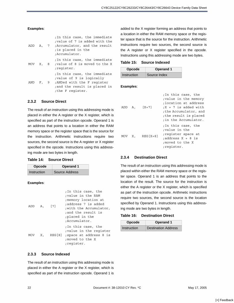
2.3.2 Source Direct
The result of an instruction using this addressing mode is
placed in either the A register or the X register, which is
specified as part of the instruction opcode. Operand 1 is
an address that points to a location in either the RAM
memory space or the register space that is the source for
the instruction. Arithmetic instructions require two
sources, the second source is the A register or X register
specified in the opcode. Instructions using this address-
ing mode are two bytes in length.
Examples:
2.3.3 Source Indexed
The result of an instruction using this addressing mode is
placed in either the A register or the X register, which is
specified as part of the instruction opcode. Operand 1 is
added to the X register forming an address that points to
a location in either the RAM memory space or the regis-
ter space that is the source for the instruction. Arithmetic
instructions require two sources, the second source is
the A register or X register specified in the opcode.
Instructions using this addressing mode are two bytes.
Examples:
2.3.4 Destination Direct
The result of an instruction using this addressing mode is
placed within either the RAM memory space or the regis-
ter space. Operand 1 is an address that points to the
location of the result. The source for the instruction is
either the A register or the X register, which is specified
as part of the instruction opcode. Arithmetic instructions
require two sources, the second source is the location
specified by Operand 1. Instructions using this address-
ing mode are two bytes in length.
ADD A, 7
;In this case, the immediate ;value of 7 is added with the ;Accumulator, and the result ;is placed in the ;Accumulator.
MOV X, 8;In this case, the immediate ;value of 8 is moved to the X ;register.
AND F, 9
;In this case, the immediate ;value of 9 is logically ;ANDed with the F register ;and the result is placed in ;the F register.
Table 14: Source Direct
Opcode Operand 1
Instruction Source Address
ADD A, [7]
;In this case, the ;value in the RAM ;memory location at ;address 7 is added ;with the Accumulator, ;and the result is ;placed in the ;Accumulator.
MOV X, REG[8]
;In this case, the ;value in the register ;space at address 8 is ;moved to the X ;register.
Table 15: Source Indexed
Opcode Operand 1
Instruction Source Index
ADD A, [X+7]
;In this case, the ;value in the memory ;location at address ;X + 7 is added with ;the Accumulator, and ;the result is placed ;in the Accumulator.
MOV X, REG[X+8]
;In this case, the ;value in the ;register space at ;address X + 8 is ;moved to the X ;register.
Table 16: Destination Direct
Opcode Operand 1
Instruction Destination Address
22 Document #: 38-12010 CY Rev. *C May 17, 2005
[+] Feedback
CPU Architecture
Examples:
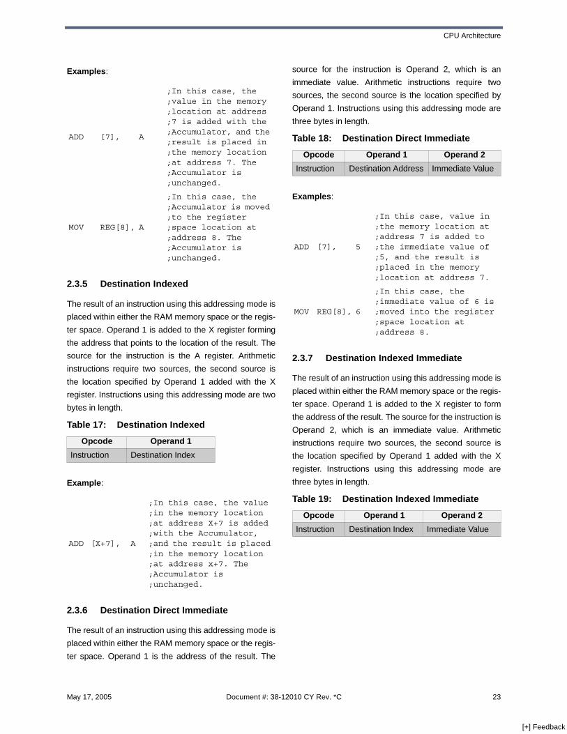
2.3.5 Destination Indexed
The result of an instruction using this addressing mode is
placed within either the RAM memory space or the regis-
ter space. Operand 1 is added to the X register forming
the address that points to the location of the result. The
source for the instruction is the A register. Arithmetic
instructions require two sources, the second source is
the location specified by Operand 1 added with the X
register. Instructions using this addressing mode are two
bytes in length.
Example:
2.3.6 Destination Direct Immediate
The result of an instruction using this addressing mode is
placed within either the RAM memory space or the regis-
ter space. Operand 1 is the address of the result. The
source for the instruction is Operand 2, which is an
immediate value. Arithmetic instructions require two
sources, the second source is the location specified by
Operand 1. Instructions using this addressing mode are
three bytes in length.
Examples:
2.3.7 Destination Indexed Immediate
The result of an instruction using this addressing mode is
placed within either the RAM memory space or the regis-
ter space. Operand 1 is added to the X register to form
the address of the result. The source for the instruction is
Operand 2, which is an immediate value. Arithmetic
instructions require two sources, the second source is
the location specified by Operand 1 added with the X
register. Instructions using this addressing mode are
three bytes in length.
ADD [7], A
;In this case, the ;value in the memory ;location at address ;7 is added with the ;Accumulator, and the ;result is placed in ;the memory location ;at address 7. The ;Accumulator is ;unchanged.
MOV REG[8], A
;In this case, the ;Accumulator is moved ;to the register ;space location at ;address 8. The ;Accumulator is ;unchanged.
Table 17: Destination Indexed
Opcode Operand 1
Instruction Destination Index
ADD [X+7], A
;In this case, the value ;in the memory location ;at address X+7 is added ;with the Accumulator, ;and the result is placed ;in the memory location ;at address x+7. The ;Accumulator is ;unchanged.
Table 18: Destination Direct Immediate
Opcode Operand 1 Operand 2
Instruction Destination Address Immediate Value
ADD [7], 5
;In this case, value in ;the memory location at ;address 7 is added to ;the immediate value of ;5, and the result is ;placed in the memory ;location at address 7.
MOV REG[8], 6
;In this case, the ;immediate value of 6 is ;moved into the register ;space location at ;address 8.
Table 19: Destination Indexed Immediate
Opcode Operand 1 Operand 2
Instruction Destination Index Immediate Value
May 17, 2005 Document #: 38-12010 CY Rev. *C 23
[+] Feedback
CY8C25122/CY8C26233/CY8C26443/CY8C26643 Device Family Data Sheet
Examples:
2.3.8 Destination Direct Direct
The result of an instruction using this addressing mode is
placed within the RAM memory. Operand 1 is the
address of the result. Operand 2 is an address that
points to a location in the RAM memory that is the source
for the instruction. This addressing mode is only valid on
the MOV instruction. The instruction using this address-
ing mode is three bytes in length.
Example:
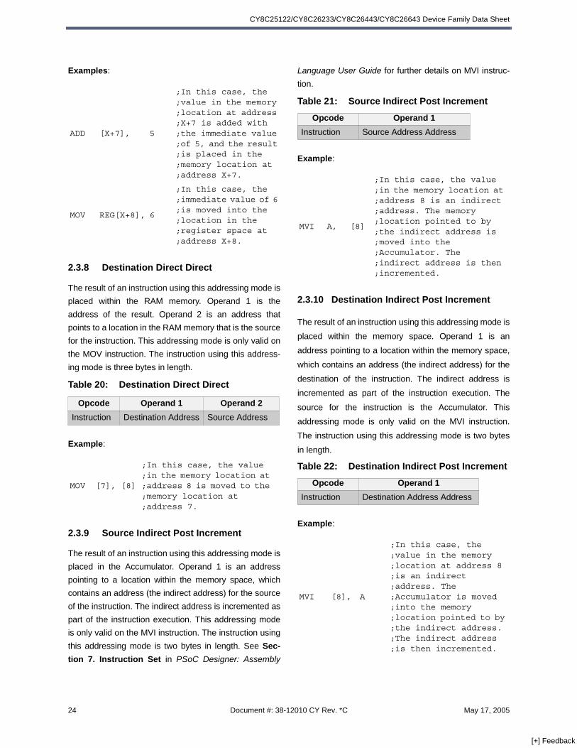
2.3.9 Source Indirect Post Increment
The result of an instruction using this addressing mode is
placed in the Accumulator. Operand 1 is an address
pointing to a location within the memory space, which
contains an address (the indirect address) for the source
of the instruction. The indirect address is incremented as
part of the instruction execution. This addressing mode
is only valid on the MVI instruction. The instruction using
this addressing mode is two bytes in length. See Sec-
tion 7. Instruction Set in PSoC Designer: Assembly
Language User Guide for further details on MVI instruc-
tion.
Example:
2.3.10 Destination Indirect Post Increment
The result of an instruction using this addressing mode is
placed within the memory space. Operand 1 is an
address pointing to a location within the memory space,
which contains an address (the indirect address) for the
destination of the instruction. The indirect address is
incremented as part of the instruction execution. The
source for the instruction is the Accumulator. This
addressing mode is only valid on the MVI instruction.
The instruction using this addressing mode is two bytes
in length.
Example:
ADD [X+7], 5
;In this case, the ;value in the memory ;location at address ;X+7 is added with ;the immediate value ;of 5, and the result ;is placed in the ;memory location at ;address X+7.
MOV REG[X+8], 6
;In this case, the ;immediate value of 6 ;is moved into the ;location in the ;register space at ;address X+8.
Table 20: Destination Direct Direct
Opcode Operand 1 Operand 2
Instruction Destination Address Source Address
MOV [7], [8]
;In this case, the value ;in the memory location at ;address 8 is moved to the ;memory location at ;address 7.
Table 21: Source Indirect Post Increment
Opcode Operand 1
Instruction Source Address Address
MVI A, [8]
;In this case, the value ;in the memory location at ;address 8 is an indirect ;address. The memory ;location pointed to by ;the indirect address is ;moved into the ;Accumulator. The ;indirect address is then ;incremented.
Table 22: Destination Indirect Post Increment
Opcode Operand 1
Instruction Destination Address Address
MVI [8], A
;In this case, the ;value in the memory ;location at address 8 ;is an indirect ;address. The ;Accumulator is moved ;into the memory ;location pointed to by ;the indirect address. ;The indirect address ;is then incremented.
24 Document #: 38-12010 CY Rev. *C May 17, 2005
[+] Feedback
CPU Architecture
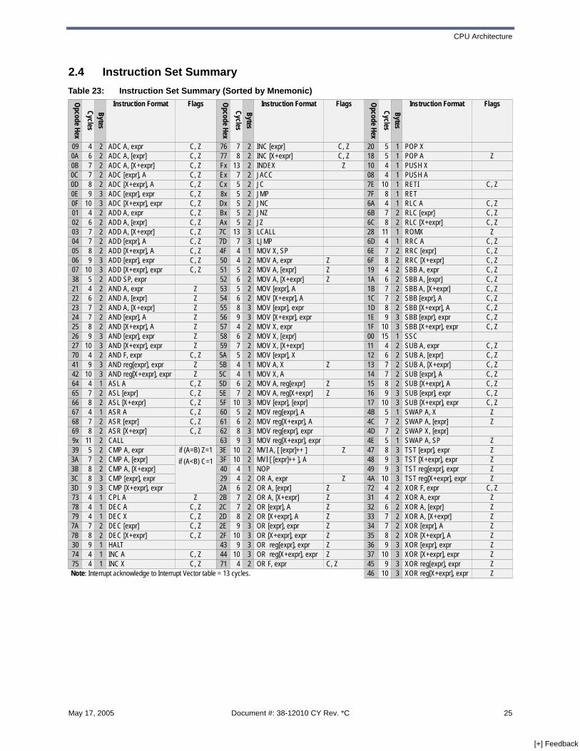
2.4 Instruction Set Summary
Table 23: Instruction Set Summary (Sorted by Mnemonic)
Opcode Hex
Cycles
Bytes
Instruction Format Flags Opcode Hex
Cycles
Bytes
Instruction Format Flags Opcode Hex
Cycles
Bytes
Instruction Format Flags
09 4 2 ADC A, expr C, Z 76 7 2 INC [expr] C, Z 20 5 1 POP X0A 6 2 ADC A, [expr] C, Z 77 8 2 INC [X+expr] C, Z 18 5 1 POP A Z0B 7 2 ADC A, [X+expr] C, Z Fx 13 2 INDEX Z 10 4 1 PUSH X0C 7 2 ADC [expr], A C, Z Ex 7 2 JACC 08 4 1 PUSH A0D 8 2 ADC [X+expr], A C, Z Cx 5 2 JC 7E 10 1 RETI C, Z0E 9 3 ADC [expr], expr C, Z 8x 5 2 JMP 7F 8 1 RET0F 10 3 ADC [X+expr], expr C, Z Dx 5 2 JNC 6A 4 1 RLC A C, Z01 4 2 ADD A, expr C, Z Bx 5 2 JNZ 6B 7 2 RLC [expr] C, Z02 6 2 ADD A, [expr] C, Z Ax 5 2 JZ 6C 8 2 RLC [X+expr] C, Z03 7 2 ADD A, [X+expr] C, Z 7C 13 3 LCALL 28 11 1 ROMX Z04 7 2 ADD [expr], A C, Z 7D 7 3 LJMP 6D 4 1 RRC A C, Z05 8 2 ADD [X+expr], A C, Z 4F 4 1 MOV X, SP 6E 7 2 RRC [expr] C, Z06 9 3 ADD [expr], expr C, Z 50 4 2 MOV A, expr Z 6F 8 2 RRC [X+expr] C, Z07 10 3 ADD [X+expr], expr C, Z 51 5 2 MOV A, [expr] Z 19 4 2 SBB A, expr C, Z38 5 2 ADD SP, expr 52 6 2 MOV A, [X+expr] Z 1A 6 2 SBB A, [expr] C, Z21 4 2 AND A, expr Z 53 5 2 MOV [expr], A 1B 7 2 SBB A, [X+expr] C, Z22 6 2 AND A, [expr] Z 54 6 2 MOV [X+expr], A 1C 7 2 SBB [expr], A C, Z23 7 2 AND A, [X+expr] Z 55 8 3 MOV [expr], expr 1D 8 2 SBB [X+expr], A C, Z24 7 2 AND [expr], A Z 56 9 3 MOV [X+expr], expr 1E 9 3 SBB [expr], expr C, Z25 8 2 AND [X+expr], A Z 57 4 2 MOV X, expr 1F 10 3 SBB [X+expr], expr C, Z26 9 3 AND [expr], expr Z 58 6 2 MOV X, [expr] 00 15 1 SSC27 10 3 AND [X+expr], expr Z 59 7 2 MOV X, [X+expr] 11 4 2 SUB A, expr C, Z70 4 2 AND F, expr C, Z 5A 5 2 MOV [expr], X 12 6 2 SUB A, [expr] C, Z41 9 3 AND reg[expr], expr Z 5B 4 1 MOV A, X Z 13 7 2 SUB A, [X+expr] C, Z42 10 3 AND reg[X+expr], expr Z 5C 4 1 MOV X, A 14 7 2 SUB [expr], A C, Z64 4 1 ASL A C, Z 5D 6 2 MOV A, reg[expr] Z 15 8 2 SUB [X+expr], A C, Z65 7 2 ASL [expr] C, Z 5E 7 2 MOV A, reg[X+expr] Z 16 9 3 SUB [expr], expr C, Z66 8 2 ASL [X+expr] C, Z 5F 10 3 MOV [expr], [expr] 17 10 3 SUB [X+expr], expr C, Z67 4 1 ASR A C, Z 60 5 2 MOV reg[expr], A 4B 5 1 SWAP A, X Z68 7 2 ASR [expr] C, Z 61 6 2 MOV reg[X+expr], A 4C 7 2 SWAP A, [expr] Z69 8 2 ASR [X+expr] C, Z 62 8 3 MOV reg[expr], expr 4D 7 2 SWAP X, [expr]9x 11 2 CALL 63 9 3 MOV reg[X+expr], expr 4E 5 1 SWAP A, SP Z39 5 2 CMP A, expr if (A=B) Z=1
if (A<B) C=1
3E 10 2 MVI A, [ [expr]++ ] Z 47 8 3 TST [expr], expr Z3A 7 2 CMP A, [expr] 3F 10 2 MVI [ [expr]++ ], A 48 9 3 TST [X+expr], expr Z3B 8 2 CMP A, [X+expr] 40 4 1 NOP 49 9 3 TST reg[expr], expr Z3C 8 3 CMP [expr], expr 29 4 2 OR A, expr Z 4A 10 3 TST reg[X+expr], expr Z3D 9 3 CMP [X+expr], expr 2A 6 2 OR A, [expr] Z 72 4 2 XOR F, expr C, Z73 4 1 CPL A Z 2B 7 2 OR A, [X+expr] Z 31 4 2 XOR A, expr Z78 4 1 DEC A C, Z 2C 7 2 OR [expr], A Z 32 6 2 XOR A, [expr] Z79 4 1 DEC X C, Z 2D 8 2 OR [X+expr], A Z 33 7 2 XOR A, [X+expr] Z7A 7 2 DEC [expr] C, Z 2E 9 3 OR [expr], expr Z 34 7 2 XOR [expr], A Z7B 8 2 DEC [X+expr] C, Z 2F 10 3 OR [X+expr], expr Z 35 8 2 XOR [X+expr], A Z30 9 1 HALT 43 9 3 OR reg[expr], expr Z 36 9 3 XOR [expr], expr Z74 4 1 INC A C, Z 44 10 3 OR reg[X+expr], expr Z 37 10 3 XOR [X+expr], expr Z75 4 1 INC X C, Z 71 4 2 OR F, expr C, Z 45 9 3 XOR reg[expr], expr ZNote: Interrupt acknowledge to Interrupt Vector table = 13 cycles. 46 10 3 XOR reg[X+expr], expr Z
May 17, 2005 Document #: 38-12010 CY Rev. *C 25
[+] Feedback
CY8C25122/CY8C26233/CY8C26443/CY8C26643 Device Family Data Sheet
3.0 Memory Organization
3.1 Flash Program Memory Organization
3.2 RAM Data Memory Organization
The stack on this device grows from low addresses to
high addresses. The Linker function within PSoC
Designer locates the bottom of the stack after the end of
Global Variables. This allows the stack to grow from just
after the Global Variables until 0xFF. The stack will wrap
back to 0x00 on an overflow condition.
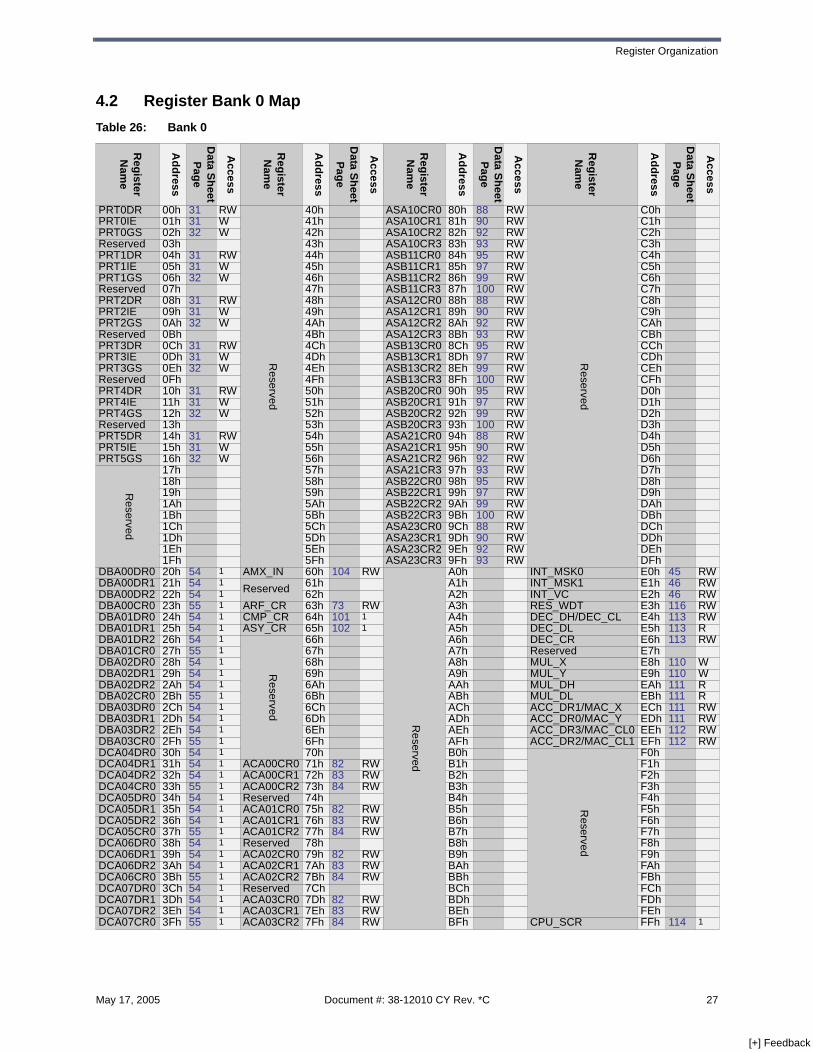
4.0 Register Organization
4.1 Introduction
There are two register banks implemented on these
devices. Each bank contains 256 addresses. The pur-
pose of these register banks is to personalize and
parameterize the on-chip resources as well as read and
write data values.
The user selects between the two banks by setting the
XIO bit in the CPU_F Flag Register.
In some cases, the same register is available on either
bank, for convenience. These registers (71h to 9fh) can
be accessed from either bank.
Note: All register addresses not shown are reserved and
should never be written. In addition, unused or reserved
bits in any register should always be written to 0.
Table 24: Flash Program Memory Map
Address Description
0x0000 Reset Vector
0x0004 Supply Monitor Interrupt Vector
0x0008 DBA 00 PSoC Block Interrupt Vector
0x000C DBA 01 PSoC Block Interrupt Vector
0x0010 DBA 02 PSoC Block Interrupt Vector
0x0014 DBA 03 PSoC Block Interrupt Vector
0x0018 DCA 04 PSoC Block Interrupt Vector
0x001C DCA 05 PSoC Block Interrupt Vector
0x0020 DCA 06 PSoC Block Interrupt Vector
0x0024 DCA 07 PSoC Block Interrupt Vector
0x0028 Analog Column 0 Interrupt Vector
0x002C Analog Column 1 Interrupt Vector
0x0030 Analog Column 2 Interrupt Vector
0x0034 Analog Column 3 Interrupt Vector
0x0038 GPIO Interrupt Vector
0x003C Sleep Timer Interrupt Vector
0x0040On-Chip User Program Memory Starts Here
***
***
***
0x3FFF16K Flash Maximum Depending on Ver-sion
Table 25: RAM Data Memory Map
Address Description
0x00 First General Purpose RAM Location
0xXX General Purpose RAM
0xXY General Purpose RAM
0xXZ Last General Purpose RAM Location
0xYX Bottom of Hardware Stack
0xYY ⇓ Stack Grows This Way ⇓0xFF Top of Hardware Stack
26 Document #: 38-12010 CY Rev. *C May 17, 2005
[+] Feedback
Register Organization
4.2 Register Bank 0 Map
Table 26: Bank 0
Reg
isterN
ame
Ad
dress
Data S
heet
Pag
e
Access
Reg
isterN
ame
Ad
dress
Data S
heet
Pag
e
Access
Reg
isterN
ame
Ad
dress
Data S
heet
Pag
e
Access
Reg
isterN
ame
Ad
dress
Data S
heet
Pag
e
Access
PRT0DR 00h 31 RW
Reserved
40h ASA10CR0 80h 88 RW
Reserved
C0hPRT0IE 01h 31 W 41h ASA10CR1 81h 90 RW C1hPRT0GS 02h 32 W 42h ASA10CR2 82h 92 RW C2hReserved 03h 43h ASA10CR3 83h 93 RW C3hPRT1DR 04h 31 RW 44h ASB11CR0 84h 95 RW C4hPRT1IE 05h 31 W 45h ASB11CR1 85h 97 RW C5hPRT1GS 06h 32 W 46h ASB11CR2 86h 99 RW C6hReserved 07h 47h ASB11CR3 87h 100 RW C7hPRT2DR 08h 31 RW 48h ASA12CR0 88h 88 RW C8hPRT2IE 09h 31 W 49h ASA12CR1 89h 90 RW C9hPRT2GS 0Ah 32 W 4Ah ASA12CR2 8Ah 92 RW CAhReserved 0Bh 4Bh ASA12CR3 8Bh 93 RW CBhPRT3DR 0Ch 31 RW 4Ch ASB13CR0 8Ch 95 RW CChPRT3IE 0Dh 31 W 4Dh ASB13CR1 8Dh 97 RW CDhPRT3GS 0Eh 32 W 4Eh ASB13CR2 8Eh 99 RW CEhReserved 0Fh 4Fh ASB13CR3 8Fh 100 RW CFhPRT4DR 10h 31 RW 50h ASB20CR0 90h 95 RW D0hPRT4IE 11h 31 W 51h ASB20CR1 91h 97 RW D1hPRT4GS 12h 32 W 52h ASB20CR2 92h 99 RW D2hReserved 13h 53h ASB20CR3 93h 100 RW D3hPRT5DR 14h 31 RW 54h ASA21CR0 94h 88 RW D4hPRT5IE 15h 31 W 55h ASA21CR1 95h 90 RW D5hPRT5GS 16h 32 W 56h ASA21CR2 96h 92 RW D6h
Reserved
17h 57h ASA21CR3 97h 93 RW D7h18h 58h ASB22CR0 98h 95 RW D8h19h 59h ASB22CR1 99h 97 RW D9h1Ah 5Ah ASB22CR2 9Ah 99 RW DAh1Bh 5Bh ASB22CR3 9Bh 100 RW DBh1Ch 5Ch ASA23CR0 9Ch 88 RW DCh1Dh 5Dh ASA23CR1 9Dh 90 RW DDh1Eh 5Eh ASA23CR2 9Eh 92 RW DEh1Fh 5Fh ASA23CR3 9Fh 93 RW DFh
DBA00DR0 20h 54 1 AMX_IN 60h 104 RW
Reserved
A0h INT_MSK0 E0h 45 RWDBA00DR1 21h 54 1
Reserved 61h A1h INT_MSK1 E1h 46 RWDBA00DR2 22h 54 1 62h A2h INT_VC E2h 46 RWDBA00CR0 23h 55 1 ARF_CR 63h 73 RW A3h RES_WDT E3h 116 RWDBA01DR0 24h 54 1 CMP_CR 64h 101 1 A4h DEC_DH/DEC_CL E4h 113 RWDBA01DR1 25h 54 1 ASY_CR 65h 102 1 A5h DEC_DL E5h 113 RDBA01DR2 26h 54 1
Reserved
66h A6h DEC_CR E6h 113 RWDBA01CR0 27h 55 1 67h A7h Reserved E7hDBA02DR0 28h 54 1 68h A8h MUL_X E8h 110 WDBA02DR1 29h 54 1 69h A9h MUL_Y E9h 110 WDBA02DR2 2Ah 54 1 6Ah AAh MUL_DH EAh 111 RDBA02CR0 2Bh 55 1 6Bh ABh MUL_DL EBh 111 RDBA03DR0 2Ch 54 1 6Ch ACh ACC_DR1/MAC_X ECh 111 RWDBA03DR1 2Dh 54 1 6Dh ADh ACC_DR0/MAC_Y EDh 111 RWDBA03DR2 2Eh 54 1 6Eh AEh ACC_DR3/MAC_CL0 EEh 112 RWDBA03CR0 2Fh 55 1 6Fh AFh ACC_DR2/MAC_CL1 EFh 112 RWDCA04DR0 30h 54 1 70h B0h
Reserved
F0hDCA04DR1 31h 54 1 ACA00CR0 71h 82 RW B1h F1hDCA04DR2 32h 54 1 ACA00CR1 72h 83 RW B2h F2hDCA04CR0 33h 55 1 ACA00CR2 73h 84 RW B3h F3hDCA05DR0 34h 54 1 Reserved 74h B4h F4hDCA05DR1 35h 54 1 ACA01CR0 75h 82 RW B5h F5hDCA05DR2 36h 54 1 ACA01CR1 76h 83 RW B6h F6hDCA05CR0 37h 55 1 ACA01CR2 77h 84 RW B7h F7hDCA06DR0 38h 54 1 Reserved 78h B8h F8hDCA06DR1 39h 54 1 ACA02CR0 79h 82 RW B9h F9hDCA06DR2 3Ah 54 1 ACA02CR1 7Ah 83 RW BAh FAhDCA06CR0 3Bh 55 1 ACA02CR2 7Bh 84 RW BBh FBhDCA07DR0 3Ch 54 1 Reserved 7Ch BCh FChDCA07DR1 3Dh 54 1 ACA03CR0 7Dh 82 RW BDh FDhDCA07DR2 3Eh 54 1 ACA03CR1 7Eh 83 RW BEh FEhDCA07CR0 3Fh 55 1 ACA03CR2 7Fh 84 RW BFh CPU_SCR FFh 114 1
May 17, 2005 Document #: 38-12010 CY Rev. *C 27
[+] Feedback
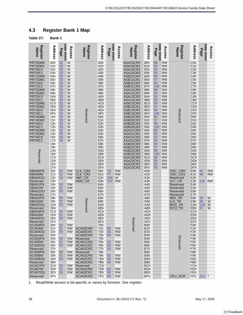
CY8C25122/CY8C26233/CY8C26443/CY8C26643 Device Family Data Sheet
4.3 Register Bank 1 Map
Table 27: Bank 1
Reg
isterN
ame
Ad
dress
Data S
heet
Pag
e
Access
Reg
isterN
ame
Ad
dress
Data S
heet
Pag
e
Access
Reg
isterN
ame
Ad
dress
Data S
heet
Pag
e
Access
Reg
isterN
ame
Ad
dress
Data S
heet
Pag
e
Access
PRT0DM0 00h 32 W
Reserved
40h ASA10CR0 80h 88 RWR
eservedC0h
PRT0DM1 01h 33 W 41h ASA10CR1 81h 90 RW C1hPRT0IC0 02h 33 W 42h ASA10CR2 82h 92 RW C2hPRT0IC1 03h 34 W 43h ASA10CR3 83h 93 RW C3hPRT1DM0 04h 32 W 44h ASB11CR0 84h 95 RW C4hPRT1DM1 05h 33 W 45h ASB11CR1 85h 97 RW C5hPRT1IC0 06h 33 W 46h ASB11CR2 86h 99 RW C6hPRT1IC1 07h 34 W 47h ASB11CR3 87h 100 RW C7hPRT2DM0 08h 32 W 48h ASA12CR0 88h 88 RW C8hPRT2DM1 09h 33 W 49h ASA12CR1 89h 90 RW C9hPRT2IC0 0Ah 33 W 4Ah ASA12CR2 8Ah 92 RW CAhPRT2IC1 0Bh 34 W 4Bh ASA12CR3 8Bh 93 RW CBhPRT3DM0 0Ch 32 W 4Ch ASB13CR0 8Ch 95 RW CChPRT3DM1 0Dh 33 W 4Dh ASB13CR1 8Dh 97 RW CDhPRT3IC0 0Eh 33 W 4Eh ASB13CR2 8Eh 99 RW CEhPRT3IC1 0Fh 34 W 4Fh ASB13CR3 8Fh 100 RW CFhPRT4DM0 10h 32 W 50h ASB20CR0 90h 95 RW D0hPRT4DM1 11h 33 W 51h ASB20CR1 91h 97 RW D1hPRT4IC0 12h 33 W 52h ASB20CR2 92h 99 RW D2hPRT4IC1 13h 34 W 53h ASB20CR3 93h 100 RW D3hPRT5DM0 14h 32 W 54h ASA21CR0 94h 88 RW D4hPRT5DM1 15h 33 W 55h ASA21CR1 95h 90 RW D5hPRT5IC0 16h 33 W 56h ASA21CR2 96h 92 RW D6hPRT5IC1 17h 34 W 57h ASA21CR3 97h 93 RW D7h
Reserved
18h 58h ASB22CR0 98h 95 RW D8h19h 59h ASB22CR1 99h 97 RW D9h1Ah 5Ah ASB22CR2 9Ah 99 RW DAh1Bh 5Bh ASB22CR3 9Bh 100 RW DBh1Ch 5Ch ASA23CR0 9Ch 88 RW DCh1Dh 5Dh ASA23CR1 9Dh 90 RW DDh1Eh 5Eh ASA23CR2 9Eh 92 RW DEh1Fh 5Fh ASA23CR3 9Fh 93 RW DFh
DBA00FN 20h 50 RW CLK_CR0 60h 76 RW
Reserved
A0h OSC_CR0 E0h 40 RWDBA00IN 21h 51 RW CLK_CR1 61h 77 RW A1h OSC_CR1 E1h 40 RWDBA00OU 22h 53 RW ABF_CR 62h 106 W A2h Reserved E2hReserved 23h AMD_CR 63h 107 RW A3h VLT_CR E3h 118 RWDBA01FN 24h 50 RW
Reserved
64h A4h Reserved E4hDBA01IN 25h 51 RW 65h A5h Reserved E5hDBA01OU 26h 53 RW 66h A6h Reserved E6hReserved 27h 67h A7h Reserved E7hDBA02FN 28h 50 RW 68h A8h IMO_TR E8h 35 WDBA02IN 29h 51 RW 69h A9h ILO_TR E9h 36 WDBA02OU 2Ah 53 RW 6Ah AAh BDG_TR EAh 120 WReserved 2Bh 6Bh ABh ECO_TR EBh 37 WDBA03FN 2Ch 50 RW 6Ch ACh
Reserved
EChDBA03IN 2Dh 51 RW 6Dh ADh EDhDBA03OU 2Eh 53 RW 6Eh AEh EEhReserved 2Fh 6Fh AFh EFhDCA04FN 30h 50 RW 70h B0h F0hDCA04IN 31h 51 RW ACA00CR0 71h 82 RW B1h F1hDCA04OU 32h 53 RW ACA00CR1 72h 83 RW B2h F2hReserved 33h ACA00CR2 73h 84 RW B3h F3hDCA05FN 34h 50 RW Reserved 74h B4h F4hDCA05IN 35h 51 RW ACA01CR0 75h 82 RW B5h F5hDCA05OU 36h 53 RW ACA01CR1 76h 83 RW B6h F6hReserved 37h ACA01CR2 77h 84 RW B7h F7hDCA06FN 38h 50 RW Reserved 78h B8h F8hDCA06IN 39h 51 RW ACA02CR0 79h 82 RW B9h F9hDCA06OU 3Ah 53 RW ACA02CR1 7Ah 83 RW BAh FAhReserved 3Bh ACA02CR2 7Bh 84 RW BBh FBhDCA07FN 3Ch 50 RW Reserved 7Ch BCh FChDCA07IN 3Dh 51 RW ACA03CR0 7Dh 82 RW BDh FDhDCA07OU 3Eh 53 RW ACA03CR1 7Eh 83 RW BEh FEhReserved 3Fh ACA03CR2 7Fh 84 RW BFh CPU_SCR FFh 114 1
1. Read/Write access is bit-specific or varies by function. See register.
28 Document #: 38-12010 CY Rev. *C May 17, 2005
[+] Feedback

I/O Ports
5.0 I/O Ports
5.1 Introduction
Up to five 8-bit-wide I/O ports (P0-P4) and one 4-bit wide
I/O port (P5) are implemented. The number of general
purpose I/Os implemented and connected to pins
depends on the individual part chosen. All port bits are
independently programmable and have the following
capabilities:
General-purpose digital input readable by the CPU.
General-purpose digital output writable by the CPU.
Independent control of data direction for each port bit.
Independent access for each port bit to Global Input and Global Output busses.
Interrupt programmable to assert on rising edge, falling edge, or change from last pin state read.
Output drive strength programmable in logic 0 and 1 states as strong, resistive (pull-up or pull-down), or high impedance.
A slew rate controlled output mode is available.
In high impedence, the digital input can be disabled to lower power consumption.
Port 1, Pin 0 is used in conjunction with device Test
Mode and does not behave the same as other I/O ports
immediately after reset. A device reset with Power On
Reset (POR) will drive P1[0] high for 8 ms immediately
after POR is released because there is a CPU hold-off
time of approximately 64 ms before code execution
begins. It will then drive P1[0] low for 8 ms. This can
impact external circuits connected to Port 1, Pin 0.
In System Sleep State, GPIO Pins P2[4] and P2[6]
should be held to a logic low or a false Low Voltage
Detect interrupt may be triggered. The cause is in the
System Sleep State, the internal Bandgap reference
generator is turned off and the reference voltage is main-
tained on a capacitor.
The circumstances are that during sleep, the reference
voltage on the capacitor is refreshed periodically at the
sleep system duty cycle. Between refresh cycles, this
voltage may leak slightly to either the positive supply or
ground. If pins P2[4] or P2[6] are in a high state, the leak-
age to the positive supply is accelerated (especially at
high temperature). Since the reference voltage is com-
pared to the supply to detect a low voltage condition, this
accelerated leakage to the positive supply voltage will
cause that voltage to appear lower than it actually is,
leading to the generation of a false Low Voltage Detect
interrupt.
Port 0 and Port 2 have additional analog input and/or
analog output capability. The specific routing and multi-
plexing of analog signals is shown in the following dia-
gram:
May 17, 2005 Document #: 38-12010 CY Rev. *C 29
[+] Feedback

CY8C25122/CY8C26233/CY8C26443/CY8C26643 Device Family Data Sheet
Figure 7: General Purpose I/O Pins
GPIOInterruptEnable(INT_MSK0:5)
Global Input Line
To CPU Bus
IM0IM1
IM0IM1
IM0IM1
GPIO Read
Global Select
D QEn
Change
Fall
Rise
Interrupt ModeIM0IM1 Output
0 0 Suppress Interrupt0 1 Falling Edge1 0 Rising Edge1 1 Change from last read
BondingPad
Analog In (Ports 0 and 2 Only)
CPU Bus
GPIO Write
5.6K
Global Select
DM0DM1
5.6K
VDD
VSS
VDD
VSS
DQ
DM0DM1
Drive ModeDM0DM1 Output
0 0 Resistive Pulldown0 1 Strong Drive1 0 High Z (off)1 1 Resistive Pullup
DM1
DM0
Global Out
DQ
1
FromOtherGPIOPins
GPIO Int
DM0DM1
Analog Out (Port 0 Only)
30 Document #: 38-12010 CY Rev. *C May 17, 2005
[+] Feedback

I/O Registers
6.0 I/O Registers
6.1 Port Data Registers
Port 0 Data Register (PRT0DR, Address = Bank 0, 00h)Port 1 Data Register (PRT1DR, Address = Bank 0, 04h)Port 2 Data Register (PRT2DR, Address = Bank 0, 08h)Port 3 Data Register (PRT3DR, Address = Bank 0, 0Ch)Port 4 Data Register (PRT4DR, Address = Bank 0, 10h)Port 5 Data Register (PRT5DR, Address = Bank 0, 14h) Note: Port 5 is 4-bits wide, Bit [3:0]
6.2 Port Interrupt Enable Registers
Port 0 Interrupt Enable Register (PRT0IE, Address = Bank 0, 01h)Port 1 Interrupt Enable Register (PRT1IE, Address = Bank 0, 05h)Port 2 Interrupt Enable Register (PRT2IE, Address = Bank 0, 09h)Port 3 Interrupt Enable Register (PRT3IE, Address = Bank 0, 0Dh)Port 4 Interrupt Enable Register (PRT4IE, Address = Bank 0, 11h)Port 5 Interrupt Enable Register (PRT5IE, Address = Bank 0, 15h) Note: Port 5 is 4-bits wide
Table 28: Port Data Registers
Bit # 7 6 5 4 3 2 1 0
POR 0 0 0 0 0 0 0 0
Read/Write RW RW RW RW RW RW RW RW
Bit Name Data [7] Data [6] Data [5] Data [4] Data [3] Data [2] Data [1] Data [0]
Bit [7:0]: Data [7:0] When written is the bits for output on port pins. When read is the state of the port pins
Table 29: Port Interrupt Enable Registers
Bit # 7 6 5 4 3 2 1 0
POR 0 0 0 0 0 0 0 0
Read/Write W W W W W W W W
Bit Name Int En [7] Int En [6] Int En [5] Int En [4] Int En [3] Int En [2] Int En [1] Int En [0]
Bit [7:0]: Int En [7:0] When written sets the pin interrupt state0 = Interrupt disabled for pin1 = Interrupt enabled for pin
May 17, 2005 Document #: 38-12010 CY Rev. *C 31
[+] Feedback
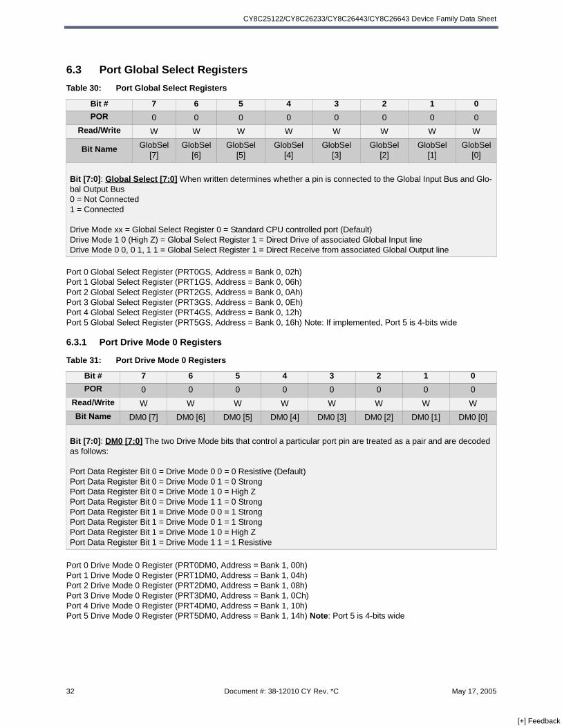
CY8C25122/CY8C26233/CY8C26443/CY8C26643 Device Family Data Sheet
6.3 Port Global Select Registers
Port 0 Global Select Register (PRT0GS, Address = Bank 0, 02h)Port 1 Global Select Register (PRT1GS, Address = Bank 0, 06h)Port 2 Global Select Register (PRT2GS, Address = Bank 0, 0Ah)Port 3 Global Select Register (PRT3GS, Address = Bank 0, 0Eh)Port 4 Global Select Register (PRT4GS, Address = Bank 0, 12h)Port 5 Global Select Register (PRT5GS, Address = Bank 0, 16h) Note: If implemented, Port 5 is 4-bits wide
6.3.1 Port Drive Mode 0 Registers
Port 0 Drive Mode 0 Register (PRT0DM0, Address = Bank 1, 00h)Port 1 Drive Mode 0 Register (PRT1DM0, Address = Bank 1, 04h)Port 2 Drive Mode 0 Register (PRT2DM0, Address = Bank 1, 08h)Port 3 Drive Mode 0 Register (PRT3DM0, Address = Bank 1, 0Ch)Port 4 Drive Mode 0 Register (PRT4DM0, Address = Bank 1, 10h)Port 5 Drive Mode 0 Register (PRT5DM0, Address = Bank 1, 14h) Note: Port 5 is 4-bits wide
Table 30: Port Global Select Registers
Bit # 7 6 5 4 3 2 1 0
POR 0 0 0 0 0 0 0 0
Read/Write W W W W W W W W
Bit Name GlobSel [7]
GlobSel [6]
GlobSel [5]
GlobSel [4]
GlobSel [3]
GlobSel [2]
GlobSel [1]
GlobSel [0]
Bit [7:0]: Global Select [7:0] When written determines whether a pin is connected to the Global Input Bus and Glo-bal Output Bus0 = Not Connected1 = Connected
Drive Mode xx = Global Select Register 0 = Standard CPU controlled port (Default)Drive Mode 1 0 (High Z) = Global Select Register 1 = Direct Drive of associated Global Input lineDrive Mode 0 0, 0 1, 1 1 = Global Select Register 1 = Direct Receive from associated Global Output line
Table 31: Port Drive Mode 0 Registers
Bit # 7 6 5 4 3 2 1 0
POR 0 0 0 0 0 0 0 0
Read/Write W W W W W W W W
Bit Name DM0 [7] DM0 [6] DM0 [5] DM0 [4] DM0 [3] DM0 [2] DM0 [1] DM0 [0]
Bit [7:0]: DM0 [7:0] The two Drive Mode bits that control a particular port pin are treated as a pair and are decoded as follows:
Port Data Register Bit 0 = Drive Mode 0 0 = 0 Resistive (Default)Port Data Register Bit 0 = Drive Mode 0 1 = 0 StrongPort Data Register Bit 0 = Drive Mode 1 0 = High ZPort Data Register Bit 0 = Drive Mode 1 1 = 0 StrongPort Data Register Bit 1 = Drive Mode 0 0 = 1 Strong Port Data Register Bit 1 = Drive Mode 0 1 = 1 StrongPort Data Register Bit 1 = Drive Mode 1 0 = High ZPort Data Register Bit 1 = Drive Mode 1 1 = 1 Resistive
32 Document #: 38-12010 CY Rev. *C May 17, 2005
[+] Feedback

I/O Registers
6.3.2 Port Drive Mode 1 Registers
Port 0 Drive Mode 1 Register (PRT0DM1, Address = Bank 1, 01h)Port 1 Drive Mode 1 Register (PRT1DM1, Address = Bank 1, 05h)Port 2 Drive Mode 1 Register (PRT2DM1, Address = Bank 1, 09h)Port 3 Drive Mode 1 Register (PRT3DM1, Address = Bank 1, 0Dh)Port 4 Drive Mode 1 Register (PRT4DM1, Address = Bank 1, 11h)Port 5 Drive Mode 1 Register (PRT5DM1, Address = Bank 1, 15h) Note: Port 5 is 4-bits wide
6.3.3 Port Interrupt Control 0 Registers
Port 0 Interrupt Control 0 Register (PRT0IC0, Address = Bank 1, 02h)Port 1 Interrupt Control 0 Register (PRT1IC0, Address = Bank 1, 06h)Port 2 Interrupt Control 0 Register (PRT2IC0, Address = Bank 1, 0Ah)Port 3 Interrupt Control 0 Register (PRT3IC0, Address = Bank 1, 0Eh)Port 4 Interrupt Control 0 Register (PRT4IC0, Address = Bank 1, 12h)Port 5 Interrupt Control 0 Register (PRT5IC0, Address = Bank 1, 16h) Note: Port 5 is 4-bits wide
Table 32: Port Drive Mode 1 Registers
Bit # 7 6 5 4 3 2 1 0
POR 0 0 0 0 0 0 0 0
Read/Write W W W W W W W W
Bit Name DM1 [7] DM1 [6] DM1 [5] DM1 [4] DM1 [3] DM1 [2] DM1 [1] DM1 [0]
Bit [7:0]: DM1 [7:0] See truth table for Port Drive Mode 0 Registers, above
Table 33: Port Interrupt Control 0 Registers
Bit # 7 6 5 4 3 2 1 0
POR 0 0 0 0 0 0 0 0
Read/Write W W W W W W W W
Bit Name IC0 [7] IC0 [6] IC0 [5] IC0 [4] IC0 [3] IC0 [2] IC0 [1] IC0 [0]
Bit [7:0]: IC0 [7:0] The two Interrupt Control bits that control a particular port pin are treated as a pair and are decoded as follows:IC1 [x], IC0 [x] = 0 0 = Disabled (Default)IC1 [x], IC0 [x] = 0 1 = Falling Edge (-)IC1 [x], IC0 [x] = 1 0 = Rising Edge (+)IC1 [x], IC0 [x] = 1 1 = Change from Last Direct Read
May 17, 2005 Document #: 38-12010 CY Rev. *C 33
[+] Feedback

CY8C25122/CY8C26233/CY8C26443/CY8C26643 Device Family Data Sheet
6.3.4 Port Interrupt Control 1 Registers
Port 0 Interrupt Control 1 Register (PRT0IC1, Address = Bank 1, 03h)Port 1 Interrupt Control 1 Register (PRT1IC1, Address = Bank 1, 07h)Port 2 Interrupt Control 1 Register (PRT2IC1, Address = Bank 1, 0Bh)Port 3 Interrupt Control 1 Register (PRT3IC1, Address = Bank 1, 0Fh)Port 4 Interrupt Control 1 Register (PRT4IC1, Address = Bank 1, 13h)Port 5 Interrupt Control 1 Register (PRT5IC1, Address = Bank 1, 17h) Note: Port 5 is 4-bits wide
Table 34: Port Interrupt Control 1 Registers
Bit # 7 6 5 4 3 2 1 0
POR 0 0 0 0 0 0 0 0Read/Write W W W W W W W W
Bit Name IC1 [7] IC1 [6] IC1 [5] IC1 [4] IC1 [3] IC1 [2] IC1 [1] IC1 [0]
Bit [7:0]: IC1 [7:0] See truth table for Port Interrupt Control 0 Registers, above
34 Document #: 38-12010 CY Rev. *C May 17, 2005
[+] Feedback

Clocking
7.0 Clocking
7.1 Oscillator Options
7.1.1 Internal Main Oscillator
The internal main oscillator outputs two frequencies, 48
MHz and 24 MHz. In the absence of a high-precision
input source from the external oscillator, the accuracy of
this circuit is +/- 2.5% (between 0oC and +85oC). No
external components are required to achieve this level of
accuracy. The Internal Main Oscillator Trim Register
(IMO_TR) is used to calibrate this oscillator into specified
tolerance. Factory-programmed trim values are available
for 5.0V and 3.3V operation. The 5.0V value is loaded in
the IMO_TR register upon reset. This register must be
adjusted when the operating voltage is outside the range
for which factory calibration was set. The factory-pro-
grammed trim value is selected using the Table Read
Supervisor Call, and is documented in 11.8.
There is an option to phase lock this oscillator to the
External Crystal Oscillator. The choice of crystal and its
inherent accuracy will determine the overall accuracy of
the oscillator. The External Crystal Oscillator must be
stable prior to locking the frequency of the Internal Main
Oscillator to this reference source.
Internal Main Oscillator Trim Register (IMO_TR, Address = Bank 1, E8h)
7.1.2 Internal Low Speed Oscillator
An internal low speed oscillator of nominally 32 kHz is
available to generate sleep wake-up interrupts and
Watchdog resets if the user does not want to attach a
32.768 kHz watch crystal. This oscillator can also be
used as a clocking source for the digital PSoC blocks.
The oscillator operates in two different modes. A trim
value is written to the Internal Low Speed Oscillator Trim
Register (ILO_TR), shown below, upon reset. See sec-
tion 13.0 for accuracy information. When the IC is put
into sleep mode this oscillator drops into an ultra low cur-
rent state and the accuracy is reduced.
This register sets the adjustment for the Internal Low
Speed Oscillator. The value placed in this register is
based on factory testing. It is recommended that the user
not alter this value.
Table 35: Internal Main Oscillator Trim Register
Bit # 7 6 5 4 3 2 1 0
POR FS1 FS1 FS1 FS1 FS1 FS1 FS1 FS1
Read/Write W W W W W W W W
Bit Name IMO Trim [7]
IMO Trim [6]
IMO Trim [5]
IMO Trim [4]
IMO Trim [3]
IMO Trim [2]
IMO Trim [1]
IMO Trim [0]
Bit [7:0]: IMO Trim [7:0] Data value stored will alter the trimmed frequency of the Internal Main Oscillator. A larger value in this register will increase the speed of the Internal Main Oscillator
1. FS = Factory set trim value
May 17, 2005 Document #: 38-12010 CY Rev. *C 35
[+] Feedback

CY8C25122/CY8C26233/CY8C26443/CY8C26643 Device Family Data Sheet
Internal Low Speed Oscillator Trim Register (ILO_TR, Address = Bank 1, E9h)
7.1.3 External Crystal Oscillator
The XtalIn and XtalOut pins support connection of a
32.768 kHz watch crystal to drive the 32K clock. To con-
nect to the external crystal, the XtalIn and XtalOut pins’
drive modes must be set to High Z. To enable the exter-
nal crystal oscillator, bit 7 of the Oscillator Control 0 Reg-
ister (OSC_CR0) must be set (default is off). Note that
the Internal Low Speed Oscillator continues to run when
this external function is selected. It runs until the oscilla-
tor is automatically switched over when the sleep timer
reaches terminal count. External feedback capacitors to
Vcc are required.
The firmware steps involved in switching between the
Internal Low Speed Oscillator and External Crystal Oscil-
lator are as follows:
1. At reset, the chip begins operation using the Internal Low Speed Oscillator.
2. User immediately selects a sleep interval of 1 sec-ond in the Oscillator Control 0 Register (OSC_CR0), as the oscillator stabilization interval.
3. User selects External Crystal Oscillator by setting bit [7] in Oscillator Control 0 Register (OSC_CR0) to 1.
4. The External Crystal Oscillator becomes the selected 32.768 kHz source at the end of the 1-sec-
ond interval, created by the Sleep Interrupt logic. The 1-second interval gives the oscillator time to stabilize before it becomes the active source. The Sleep Interrupt need not be enabled for the switch over to occur. The user may want to reset the sleep timer (if this does not interfere with any ongoing real-time clock operation), to guarantee the interval length.
5. The user must wait the 1-second stabilization period prior to engaging the PLL mode to lock the Internal Main Oscillator frequency to the External Crystal Oscillator frequency.
If the proper settings are selected in PSoC Designer, the
above steps are automatically done in boot.asm.
Note: Transitions between oscillator domains may pro-
duce glitches on the 32K clock bus. Functions that
require accuracy on the 32K clock should be enabled
after the transition in oscillator domains.
The External Crystal Oscillator Trim Register (ECO_TR)
sets the adjustment for the External Crystal Oscillator.
The value placed in this register at reset is based on fac-
tory testing. This register does not adjust the frequency
of the External Crystal Oscillator. It is recommended that
the user not alter this value.
Table 36: Internal Low Speed Oscillator Trim Register
Bit # 7 6 5 4 3 2 1 0
POR 0 0 FS1
1. FS = Factory set trim value
FS1 FS1 FS1 FS1 FS1
Read/Write -- W W W W W W W
Bit Name Reserved DisableILO Trim
[5]ILO Trim
[4]ILO Trim
[3]ILO Trim
[2]ILO Trim
[1]ILO Trim
[0]
Bit 7: Reserved
Bit 6: Disable0 = Low Speed Oscillator is on1 = Low Speed Oscillator is off (minimum power state)
Bit [5:0]: ILO Trim [5:0] Data value stored will alter the trimmed frequency of the Internal Low Speed Oscillator. (Not recommended for customer alteration)
36 Document #: 38-12010 CY Rev. *C May 17, 2005
[+] Feedback
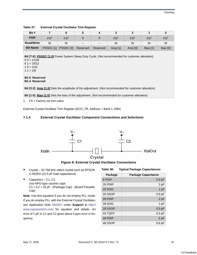
Clocking
External Crystal Oscillator Trim Register (ECO_TR, Address = Bank 1, EBh)
7.1.4 External Crystal Oscillator Component Connections and Selections
Crystal – 32.768 kHz watch crystal such as EPSON C-002RX (12.5 pF load capacitance)
Capacitors – C1, C2Use NPO-type ceramic capsC1 = C2 = 25 pF - (Package Cap) - (Board Parasitic Cap)
Note: Use this equation if you do not employ PLL mode.
If you do employ PLL with the External Crystal Oscillator,
see Application Note AN2027 under Support at http://
www.cypressmicro.com for equation and details. An
error of 1 pF in C1 and C2 gives about 3 ppm error in fre-
quency.
Table 37: External Crystal Oscillator Trim Register
Bit # 7 6 5 4 3 2 1 0
POR FS1
1. FS = Factory set trim value
FS1 0 0 FS1 FS1 FS1 FS1
Read/Write W W -- -- W W W W
Bit Name PSSDC [1] PSSDC [0] Reserved Reserved Amp [1] Amp [0] Bias [1] Bias [0]
Bit [7:6]: PSSDC [1:0] Power System Sleep Duty Cycle. (Not recommended for customer alteration)0 0 = 1/1280 1 = 1/5121 0 = 1/321 1 = 1/8
Bit 5: Reserved Bit 4: Reserved
Bit [3:2]: Amp [1:0] Sets the amplitude of the adjustment. (Not recommended for customer alteration)
Bit [1:0]: Bias [1:0] Sets the bias of the adjustment. (Not recommended for customer alteration)
Figure 8: External Crystal Oscillator Connections
XtalIn XtalOut
Crystal
C1 C2
VccVcc
Table 38: Typical Package Capacitances
Package Package Capacitance
8 PDIP 0.9 pF
20 PDIP 2 pF
20 SOIC 1 pF
20 SSOP 0.5 pF
28 PDIP 2 pF
28 SOIC 1 pF
28 SSOP 0.5 pF
44 TQFP 0.5 pF
48 PDIP 5 pF
48 SSOP 0.6 pF
May 17, 2005 Document #: 38-12010 CY Rev. *C 37
[+] Feedback

CY8C25122/CY8C26233/CY8C26443/CY8C26643 Device Family Data Sheet
7.1.5 Phase-Locked Loop (PLL) Operation
The Phase-Locked Loop (PLL) function generates the
system clock with crystal accuracy. It is designed to pro-
vide a 23.986 MHz oscillator when utilized with an exter-
nal 32.768 kHz crystal. Although the PLL provides
crystal accuracy it requires time to lock onto the refer-
ence frequency when first starting. After the External
Crystal Oscillator has been selected and enabled, the
following procedure should be followed to enable the
PLL and allow for proper frequency lock:
1. Select a CPU frequency of 3 MHz or less.
2. Enable the PLL.
3. Wait at least 10 ms.
4. Set CPU to a faster frequency, if desired. To do this, write the bits CPU[2:0] in the OSC_CR0 register.
The CPU frequency will immediately change when these bits are set.
If the proper settings are selected in PSoC Designer, the
above steps are automatically done in boot.asm.
7.2 System Clocking Signals
There are twelve system-clocking signals that are used
throughout the device. Referenced frequencies are
based on use of 32.768 kHz crystal. The names of these
signals and their definitions are as follows:
Table 39: System Clocking Signals and Definitions
Signal Definition
48M The direct 48 MHz output from the Internal Main Oscillator.
24M The direct 24 MHz output from the Internal Main Oscillator.
24V1
The 24 MHz output from the Internal Main Oscillator that has been passed through a user-selectable 1 to 16 divider F = 24 MHz / (1 to 16) = 24 MHz to 1.5 MHz. The divider value is found in the Oscillator Control 1 Register (OSC_CR1). Note that the divider will be N+1, based on a value of N written into the register bits.
24V2
The 24V1 signal that has been passed through an additional user-selectable 1 to 16 divider F = 24 MHz / ((1 to 16) * (1 to 16)) = 24 MHz to 93.7 kHz. The divider value is found in the Oscillator Control 1 Register (OSC_CR1). Note that the divider will be N+1, based on a value of N written into the register bits.
32K The multiplexed output of either the Internal Low Speed Oscillator or the External Crystal Oscillator.
CPUThe output from the Internal Main Oscillator that has been passed through a divider that has 8 user selectable ratios ranging from 1:1 to 1:256, yielding frequencies ranging from 24 MHz to 93.7 kHz.
SLPThe 32K system-clocking signal that has been passed through a divider that has 4 user selectable
ratios ranging from 1:26 to 1:215, yielding frequencies ranging from 512 Hz to 1 Hz. This signal is used to clock the sleep timer period.
38 Document #: 38-12010 CY Rev. *C May 17, 2005
[+] Feedback

Clocking
The following diagram shows the PSoC MCU Clock Tree of signals 48M through SLP:
7.2.1 CPU and Sleep Timer Clock Options
The CPU is clocked off the CPU system-clocking signal,
which can be configured to run at one of eight rates. This
selection is independent from all other clock selection
functions. It is completely safe for the CPU to change its
clock rate without a timing hazard. The CPU clock period
is determined by setting the CPU[2:0] bits in the Oscilla-
tor Control 0 Register (OSC_CR0).
The sleep timer is clocked off the SLP system-clocking
signal. The SLEEP[1] and SLEEP[0] bits in the Oscillator
Control 0 Register (OSC_CR0) allow the user to select
from the four available periods.
Figure 9: PSoC MCU Clock Tree of Signals
InternalMain
Oscillator
ExternalCrystal
Oscillator
InternalLow SpeedOscillator
48M
24M
÷ n24V1
24V2
CPU
32K
SLP
48 MHz
24 MHz
IMO_TR[7:0]OSC_CR0[6]
OSC_CR1[7:4]
OSC_CR1[3:0]
OSC_CR0[2:0]
ECO_TR[7:0]
ILO_TR[7:0] OSC_CR0[7]
OSC_CR0[4:3]
P1[1]
P1[0]
Vcc
Vcc
÷ 1÷ 2÷ 4÷ 8÷ 16÷ 32÷ 128÷ 256
PLL Lock Enable IMO Trim Register
ECO Trim Register
ILO Trim Register
24V1 Clock Div isor
24V2 Clock Div isor
CPU Clock Div isor
Sleep Clock Div isor
32 kHz Select
÷ 732
÷ n
÷ 26
÷ 29
÷ 212
÷ 215
PhaseLock Loop
May 17, 2005 Document #: 38-12010 CY Rev. *C 39
[+] Feedback

CY8C25122/CY8C26233/CY8C26443/CY8C26643 Device Family Data Sheet
Oscillator Control 0 Register (OSC_CR0, Address = Bank 1, E0h)
Oscillator Control 1 Register (OSC_CR1, Address = Bank 1, E1h)
Table 40: Oscillator Control 0 Register
Bit # 7 6 5 4 3 2 1 0
POR 0 0 0 0 0 0 0 0Read/Write RW RW RW RW RW RW RW RW
Bit Name 32k Select PLL Mode Reserved Sleep [1] Sleep [0] CPU [2] CPU [1] CPU [0]
Bit 7: 32k Select0 = Internal low precision 32 kHz oscillator1 = External Crystal Oscillator
Bit 6: PLL Mode0 = Disabled1 = Enabled, Internal Main Oscillator is locked to External Crystal Oscillator
Bit 5: Reserved
Bit [4:3]: Sleep [1:0]0 0 = 512 Hz or 1.95 ms period0 1 = 64 Hz or 15.6 ms period1 0 = 8 Hz or 125 ms period1 1 = 1 Hz or 1 s period
Bit [2:0]: CPU [2:0]0 0 0 = 3 MHz0 0 1 = 6 MHz0 1 0 = 12 MHz0 1 1 = 24 MHz1 0 0 = 1.5 MHz1 0 1 = 750 kHz1 1 0 = 187.5 kHz1 1 1 = 93.7 kHz
Table 41: Oscillator Control 1 Register
Bit # 7 6 5 4 3 2 1 0
POR 0 0 0 0 0 0 0 0Read/Write RW RW RW RW RW RW RW RW
Bit Name 24V1 [3] 24V1 [2] 24V1 [1] 24V1 [0] 24V2 [3] 24V2 [2] 24V2 [1] 24V2 [0]
Bit [7:4]: 24V1 [3:0] 4-bit data value determines the divider value for the 24V1 system-clocking signal. Note that the 4-bit data value equals n-1, where n is the desired divider value, as illustrated in PSoC MCU Clock Tree of Signals. See Table 42 on page 41.
Bit [3:0]: 24V2 [3:0] 4-bit data value determines the divider value for the 24V2 system-clocking signal. Note that the 4-bit data value equals n-1, where n is the desired divider value, as illustrated in the PSoC MCU Clock Tree of Sig-nals. See Table 42 on page 41.
40 Document #: 38-12010 CY Rev. *C May 17, 2005
[+] Feedback

Clocking
7.2.2 24V1/24V2 Frequency Selection
The following table shows the resulting frequencies for
24V1 and 24V2 based on the value written to the
OSC_CR1 register.
Table 42: 24V1/24V2 Frequency Selection
Reg. Value
24V1 MHz 24V2 kHz Reg.
Value24V1 MHz 24V2 kHz Reg.
Value24V1 MHz 24V2 kHz Reg.
Value24V1 MHz 24V2 kHz
00 24.00 24000.00 40 4.80 4800.00 80 2.67 2666.67 C0 1.85 1846.1501 24.00 12000.00 41 4.80 2400.00 81 2.67 1333.33 C1 1.85 923.0802 24.00 8000.00 42 4.80 1600.00 82 2.67 888.89 C2 1.85 615.3803 24.00 6000.00 43 4.80 1200.00 83 2.67 666.67 C3 1.85 461.5404 24.00 4800.00 44 4.80 960.00 84 2.67 533.33 C4 1.85 369.2305 24.00 4000.00 45 4.80 800.00 85 2.67 444.44 C5 1.85 307.6906 24.00 3428.57 46 4.80 685.71 86 2.67 380.95 C6 1.85 263.7407 24.00 3000.00 47 4.80 600.00 87 2.67 333.33 C7 1.85 230.7708 24.00 2666.67 48 4.80 533.33 88 2.67 296.30 C8 1.85 205.1309 24.00 2400.00 49 4.80 480.00 89 2.67 266.67 C9 1.85 184.620A 24.00 2181.82 4A 4.80 436.36 8A 2.67 242.42 CA 1.85 167.830B 24.00 2000.00 4B 4.80 400.00 8B 2.67 222.22 CB 1.85 153.850C 24.00 1846.15 4C 4.80 369.23 8C 2.67 205.13 CC 1.85 142.010D 24.00 1714.29 4D 4.80 342.86 8D 2.67 190.48 CD 1.85 131.870E 24.00 1600.00 4E 4.80 320.00 8E 2.67 177.78 CE 1.85 123.080F 24.00 1500.00 4F 4.80 300.00 8F 2.67 166.67 CF 1.85 115.3810 12.00 12000.00 50 4.00 4000.00 90 2.40 2400.00 D0 1.71 1714.2911 12.00 6000.00 51 4.00 2000.00 91 2.40 1200.00 D1 1.71 857.1412 12.00 4000.00 52 4.00 1333.33 92 2.40 800.00 D2 1.71 571.4313 12.00 3000.00 53 4.00 1000.00 93 2.40 600.00 D3 1.71 428.5714 12.00 2400.00 54 4.00 800.00 94 2.40 480.00 D4 1.71 342.8615 12.00 2000.00 55 4.00 666.67 95 2.40 400.00 D5 1.71 285.7116 12.00 1714.29 56 4.00 571.43 96 2.40 342.86 D6 1.71 244.9017 12.00 1500.00 57 4.00 500.00 97 2.40 300.00 D7 1.71 214.2918 12.00 1333.33 58 4.00 444.44 98 2.40 266.67 D8 1.71 190.4819 12.00 1200.00 59 4.00 400.00 99 2.40 240.00 D9 1.71 171.431A 12.00 1090.91 5A 4.00 363.64 9A 2.40 218.18 DA 1.71 155.841B 12.00 1000.00 5B 4.00 333.33 9B 2.40 200.00 DB 1.71 142.861C 12.00 923.08 5C 4.00 307.69 9C 2.40 184.62 DC 1.71 131.871D 12.00 857.14 5D 4.00 285.71 9D 2.40 171.43 DD 1.71 122.451E 12.00 800.00 5E 4.00 266.67 9E 2.40 160.00 DE 1.71 114.291F 12.00 750.00 5F 4.00 250.00 9F 2.40 150.00 DF 1.71 107.1420 8.00 8000.00 60 3.43 3428.57 A0 2.18 2181.82 E0 1.60 1600.0021 8.00 4000.00 61 3.43 1714.29 A1 2.18 1090.91 E1 1.60 800.0022 8.00 2666.67 62 3.43 1142.86 A2 2.18 727.27 E2 1.60 533.3323 8.00 2000.00 63 3.43 857.14 A3 2.18 545.45 E3 1.60 400.0024 8.00 1600.00 64 3.43 685.71 A4 2.18 436.36 E4 1.60 320.0025 8.00 1333.33 65 3.43 571.43 A5 2.18 363.64 E5 1.60 266.6726 8.00 1142.86 66 3.43 489.80 A6 2.18 311.69 E6 1.60 228.5727 8.00 1000.00 67 3.43 428.57 A7 2.18 272.73 E7 1.60 200.0028 8.00 888.89 68 3.43 380.95 A8 2.18 242.42 E8 1.60 177.7829 8.00 800.00 69 3.43 342.86 A9 2.18 218.18 E9 1.60 160.002A 8.00 727.27 6A 3.43 311.69 AA 2.18 198.35 EA 1.60 145.452B 8.00 666.67 6B 3.43 285.71 AB 2.18 181.82 EB 1.60 133.332C 8.00 615.38 6C 3.43 263.74 AC 2.18 167.83 EC 1.60 123.082D 8.00 571.43 6D 3.43 244.90 AD 2.18 155.84 ED 1.60 114.292E 8.00 533.33 6E 3.43 228.57 AE 2.18 145.45 EE 1.60 106.672F 8.00 500.00 6F 3.43 214.29 AF 2.18 136.36 EF 1.60 100.0030 6.00 6000.00 70 3.00 3000.00 B0 2.00 2000.00 F0 1.50 1500.0031 6.00 3000.00 71 3.00 1500.00 B1 2.00 1000.00 F1 1.50 750.0032 6.00 2000.00 72 3.00 1000.00 B2 2.00 666.67 F2 1.50 500.0033 6.00 1500.00 73 3.00 750.00 B3 2.00 500.00 F3 1.50 375.0034 6.00 1200.00 74 3.00 600.00 B4 2.00 400.00 F4 1.50 300.0035 6.00 1000.00 75 3.00 500.00 B5 2.00 333.33 F5 1.50 250.0036 6.00 857.14 76 3.00 428.57 B6 2.00 285.71 F6 1.50 214.2937 6.00 750.00 77 3.00 375.00 B7 2.00 250.00 F7 1.50 187.5038 6.00 666.67 78 3.00 333.33 B8 2.00 222.22 F8 1.50 166.6739 6.00 600.00 79 3.00 300.00 B9 2.00 200.00 F9 1.50 150.003A 6.00 545.45 7A 3.00 272.73 BA 2.00 181.82 FA 1.50 136.363B 6.00 500.00 7B 3.00 250.00 BB 2.00 166.67 FB 1.50 125.003C 6.00 461.54 7C 3.00 230.77 BC 2.00 153.85 FC 1.50 115.383D 6.00 428.57 7D 3.00 214.29 BD 2.00 142.86 FD 1.50 107.143E 6.00 400.00 7E 3.00 200.00 BE 2.00 133.33 FE 1.50 100.003F 6.00 375.00 7F 3.00 187.5 BF 2.00 125.00 FF 1.50 93.75
May 17, 2005 Document #: 38-12010 CY Rev. *C 41
[+] Feedback
CY8C25122/CY8C26233/CY8C26443/CY8C26643 Device Family Data Sheet
7.2.3 Digital PSoC Block Clocking Options
All digital PSoC block clocks are a user-selectable
choice of 48M, 24V1, 24V2, or 32K, as well as clocking
signals from other digital PSoC blocks or general pur-
pose I/O pins. There are a total of 16 possible clock
options for each digital PSoC block. See the Digital
PSoC Block section for details.
8.0 Interrupts
8.1 Overview
Interrupts can be generated by the General Purpose I/O
lines, the Power monitor, the internal Sleep Timer, the
eight Digital PSoC blocks, and the four analog columns.
Every interrupt has a separate enable bit, which is con-
tained in the General Interrupt Mask Register
(INT_MSK0) and the Digital PSoC Block Interrupt Mask
Register (INT_MSK1). When the user writes a “1” to a
particular bit position, this enables the interrupt associ-
ated with that position. There is a single Global Interrupt
Enable bit in the Flags Register (CPU_F), which can dis-
able all interrupts, or enable those interrupts that also
have their individual interrupt bit enabled. During a reset,
the enable bits in the General Interrupt Mask Register
(INT_MASK0), the enable bits in the Digital PSoC Block
Interrupt Mask Register (INT_MSK1) and the Global
Interrupt Enable bit in the Flags Register (CPU_F) are all
cleared. The Interrupt Vector Register (INT_VC) holds
the interrupt vector for the highest priority pending inter-
rupt when read, and when written will clear all pending
interrupts.
If there is only one interrupt pending and an instruction is
executed that would mask that pending interrupt (by
clearing the corresponding bit in either of the interrupt
mask registers at address E0h or E1h in Bank 0), the
CPU will take that interrupt. Since the pending interrupt
has been cleared and there are no others, the resulting
interrupt vector is 0000h and the CPU will jump to the
user code at the beginning of Flash. To address this
issue, use the macro defined in m8c.inc called
"M8C_DisableIntMask" in PSoC Designer. This macro
brackets the register write with a disable then an enable
of global interrupts.
42 Document #: 38-12010 CY Rev. *C May 17, 2005
[+] Feedback
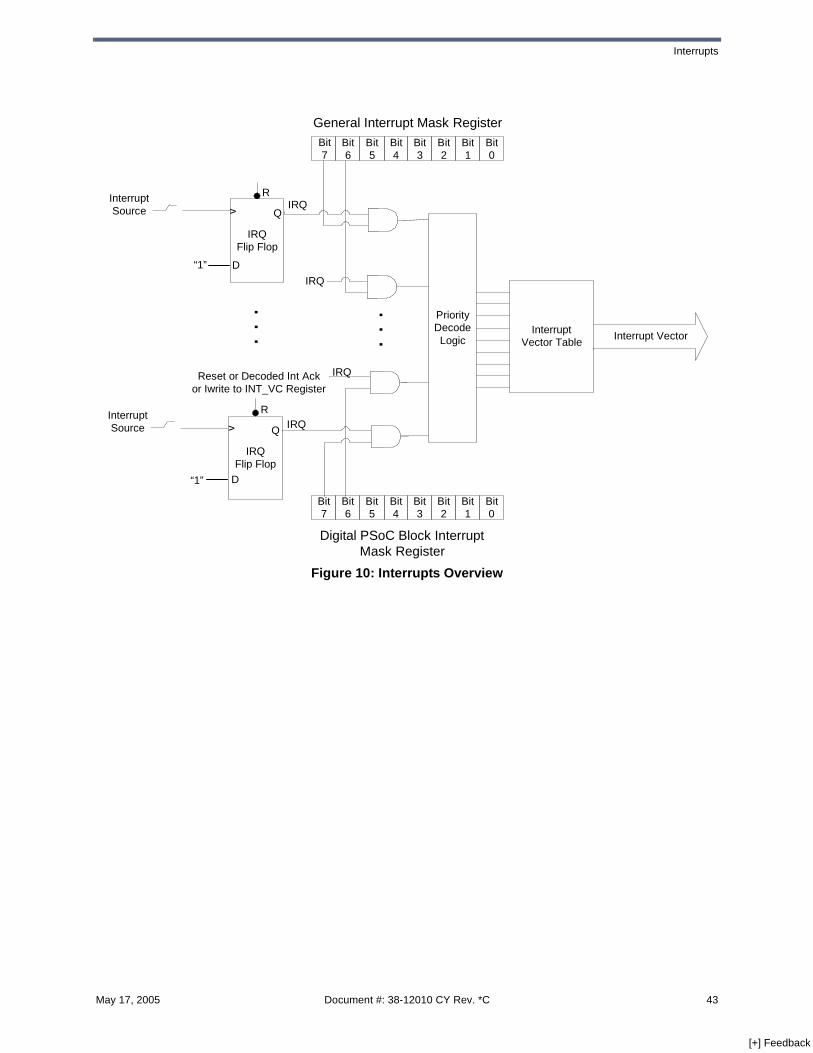
Interrupts
Figure 10: Interrupts Overview
PriorityDecodeLogic
InterruptVector Table
Interrupt Vector
Bit7
Bit0
Bit1
Bit2
Bit3
Bit4
Bit5
Bit6
Bit7
Bit0
Bit1
Bit2
Bit3
Bit4
Bit5
Bit6
General Interrupt Mask Register
Digital PSoC Block InterruptMask Register
IRQ
IRQ
...
IRQFlip Flop
RInterruptSource Q
IRQ
IRQFlip Flop
R
v
D
InterruptSource Q IRQ
“1”
Reset or Decoded Int Ackor Iwrite to INT_VC Register
...
“1” D
v
May 17, 2005 Document #: 38-12010 CY Rev. *C 43
[+] Feedback
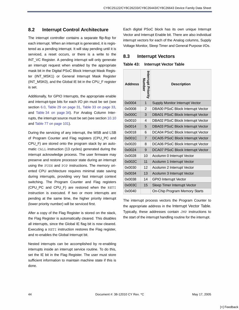
CY8C25122/CY8C26233/CY8C26443/CY8C26643 Device Family Data Sheet
8.2 Interrupt Control Architecture
The interrupt controller contains a separate flip-flop for
each interrupt. When an interrupt is generated, it is regis-
tered as a pending interrupt. It will stay pending until it is
serviced, a reset occurs, or there is a write to the
INT_VC Register. A pending interrupt will only generate
an interrupt request when enabled by the appropriate
mask bit in the Digital PSoC Block Interrupt Mask Regis-
ter (INT_MSK1) or General Interrupt Mask Register
(INT_MSK0), and the Global IE bit in the CPU_F register
is set.
Additionally, for GPIO Interrupts, the appropriate enable
and interrupt-type bits for each I/O pin must be set (see
section 6.0, Table 29 on page 31, Table 33 on page 33,
and Table 34 on page 34). For Analog Column Inter-
rupts, the interrupt source must be set (see section 10.10
and Table 77 on page 101).
During the servicing of any interrupt, the MSB and LSB
of Program Counter and Flag registers (CPU_PC and
CPU_F) are stored onto the program stack by an auto-
matic CALL instruction (13 cycles) generated during the
interrupt acknowledge process. The user firmware may
preserve and restore processor state during an interrupt
using the PUSH and POP instructions. The memory ori-
ented CPU architecture requires minimal state saving
during interrupts, providing very fast interrupt context
switching. The Program Counter and Flag registers
(CPU_PC and CPU_F) are restored when the RETI
instruction is executed. If two or more interrupts are
pending at the same time, the higher priority interrupt
(lower priority number) will be serviced first.
After a copy of the Flag Register is stored on the stack,
the Flag Register is automatically cleared. This disables
all interrupts, since the Global IE flag bit is now cleared.
Executing a RETI instruction restores the Flag register,
and re-enables the Global Interrupt bit.
Nested interrupts can be accomplished by re-enabling
interrupts inside an interrupt service routine. To do this,
set the IE bit in the Flag Register. The user must store
sufficient information to maintain machine state if this is
done.
Each digital PSoC block has its own unique Interrupt
Vector and Interrupt Enable bit. There are also individual
interrupt vectors for each of the Analog columns, Supply
Voltage Monitor, Sleep Timer and General Purpose I/Os.
8.3 Interrupt Vectors
The interrupt process vectors the Program Counter to
the appropriate address in the Interrupt Vector Table.
Typically, these addresses contain JMP instructions to
the start of the interrupt handling routine for the interrupt.
Table 43: Interrupt Vector Table
Address
Interru
pt P
riority
Nu
mb
er
Description
0x0004 1 Supply Monitor Interrupt Vector
0x0008 2 DBA00 PSoC Block Interrupt Vector
0x000C 3 DBA01 PSoC Block Interrupt Vector
0x0010 4 DBA02 PSoC Block Interrupt Vector
0x0014 5 DBA03 PSoC Block Interrupt Vector
0x0018 6 DCA04 PSoC Block Interrupt Vector
0x001C 7 DCA05 PSoC Block Interrupt Vector
0x0020 8 DCA06 PSoC Block Interrupt Vector
0x0024 9 DCA07 PSoC Block Interrupt Vector
0x0028 10 Acolumn 0 Interrupt Vector
0x002C 11 Acolumn 1 Interrupt Vector
0x0030 12 Acolumn 2 Interrupt Vector
0x0034 13 Acolumn 3 Interrupt Vector
0x0038 14 GPIO Interrupt Vector
0x003C 15 Sleep Timer Interrupt Vector
0x0040 On-Chip Program Memory Starts
44 Document #: 38-12010 CY Rev. *C May 17, 2005
[+] Feedback

Interrupts
8.4 Interrupt Masks
General Interrupt Mask Register (INT_MSK0, Address = Bank 0, E0h)
Table 44: General Interrupt Mask Register
Bit # 7 6 5 4 3 2 1 0
POR 0 0 0 0 0 0 0 0Read/Write RW RW RW RW RW RW RW RW
Bit Name Reserved Sleep GPIO Acolumn3 Acolumn2 Acolumn1 Acolumn0 Voltage Monitor
Bit 7: Reserved
Bit 6: Sleep Interrupt Enable Bit (see 11.4)0 = Disabled1 = Enabled
Bit 5: GPIO Interrupt Enable Bit (see 8.6)0 = Disabled1 = Enabled
Bit [4]: Acolumn 3 Interrupt Enable Bit (see 10.0)0 = Disabled1 = Enabled
Bit [3]: Acolumn 2 Interrupt Enable Bit (see 10.0)0 = Disabled1 = Enabled
Bit [2]: Acolumn 1 Interrupt Enable Bit (see 10.0)0 = Disabled1 = Enabled
Bit [1]: Acolumn 0 Interrupt Enable Bit (see 10.0)0 = Disabled1 = Enabled
Bit 0: Voltage Monitor Interrupt Enable Bit (see 11.5)0 = Disabled1 = Enabled
May 17, 2005 Document #: 38-12010 CY Rev. *C 45
[+] Feedback

CY8C25122/CY8C26233/CY8C26443/CY8C26643 Device Family Data Sheet
Digital PSoC Block Interrupt Mask Register (INT_MSK1, Address = Bank 0, E1h)
8.5 Interrupt Vector Register
Interrupt Vector Register (INT_VC, Address = Bank 0, E2h)
Table 45: Digital PSoC Block Interrupt Mask Register
Bit # 7 6 5 4 3 2 1 0
POR 0 0 0 0 0 0 0 0
Read/Write RW RW RW RW RW RW RW RW
Bit Name DCA07 DCA06 DCA05 DCA04 DBA03 DBA02 DBA01 DBA00
Bit 7: DCA07 Interrupt Enable Bit 0 = Disabled1 = Enabled
Bit 6: DCA06 Interrupt Enable Bit 0 = Disabled1 = Enabled
Bit 5: DCA05 Interrupt Enable Bit 0 = Disabled1 = Enabled
Bit 4: DCA04 Interrupt Enable Bit 0 = Disabled1 = Enabled
Bit 3: DBA03 Interrupt Enable Bit 0 = Disabled1 = Enabled
Bit 2: DBA02 Interrupt Enable Bit 0 = Disabled1 = Enabled
Bit 1: DBA01 Interrupt Enable Bit 0 = Disabled1 = Enabled
Bit 0: DBA00 Interrupt Enable Bit 0 = Disabled1 = Enabled
Table 46: Interrupt Vector Register
Bit # 7 6 5 4 3 2 1 0
POR 0 0 0 0 0 0 0 0
Read/Write RW RW RW RW RW RW RW RW
Bit Name Data[7] Data[6] Data[5] Data[4] Data[3] Data[2] Data[1] Data[0]
Bit [7:0]: Data [7:0] 8-bit data value holds the interrupt vector for the highest priority pending interrupt. Writing to this register will clear all pending interrupts
46 Document #: 38-12010 CY Rev. *C May 17, 2005
[+] Feedback

Interrupts
8.6 GPIO Interrupt
GPIO Interrupts are polarity configurable and pin-wise
maskable (within each Port’s pin configuration registers).
They all share the same interrupt priority and vector.
Any general purpose I/O can be used as an interrupt
source. The GPIO bit in the General Interrupt Mask Reg-
ister (INT_MSK0) must be set to enable pin interrupts, as
well as the enable bits for each pin, which are located in
the Port x Interrupt Enable Registers (PRTxIE). There
are user selectable options to generate an interrupt on 1)
any change from the last read state, 2) rising edge, and
3) falling edge.
When Interrupt on Change is selected, the state of the
GPIO pin is stored when the port is read. Changes from
this state will then assert the interrupt, if enabled.
For a GPIO interrupt to occur, the following steps must
be taken:
1. The pin Drive Mode must be set so the pin can be an input.
2. The pin must be enabled to generate an interrupt by setting the appropriate bit in the Port interrupt Enable Register (PRTxIE).
3. The edge type for the interrupt must be set in the Port Interrupt Control 0 and Control 1 Registers (PRTxIC0 and PRTxIC1). Edge type must be set to a value other than 00.
4. The GPIO bit must be set in the General Interrupt Mask Register (INT_MSK0).
5. The Global Interrupt Enable bit must be set.
6. Because the GPIO interrupts all share the same interrupt vector, the source for the GPIO interrupt must be cleared before any other GPIO interrupt will occur (i.e., the OR gate in Figure 11: “ors” all of the INTOUTn signals together). If any of the INTOUTn signals are high, the flip-flop in Figure 11: will not see a rising edge and no IRQ will occur.
Figure 11: GPIO Interrupt Enable Diagram
RD IRQ
To PriorityDecode Logic
GPIO Int EnableBIT S, INT_MSK0
QAll GPIO INTOUTs
Int Logic
GPIO BIT IEPORTX IE Register(PRT0IE...PRT5IE)
INTOUTn
GPIO Cell
PIN
“1”
OR
May 17, 2005 Document #: 38-12010 CY Rev. *C 47
[+] Feedback

CY8C25122/CY8C26233/CY8C26443/CY8C26643 Device Family Data Sheet
9.0 Digital PSoC Blocks
9.1 Introduction
PSoC blocks are user configurable system resources.
On-chip digital PSoC blocks reduce the need for many
MCU part types and external peripheral components.
Digital PSoC blocks can be configured to provide a wide
variety of peripheral functions. PSoC Designer Software
Integrated Development Environment provides auto-
mated configuration of PSoC blocks by simply selecting
the desired functions. PSoC Designer then generates
the proper configuration information and can print a
device data sheet unique to that configuration.
Digital PSoC blocks provide up to eight, 8-bit multipur-
pose timers/counters supporting multiple event timers,
real-time clocks, Pulse Width Modulators (PWM), and
CRCs. In addition to all PSoC block functions, communi-
cation PSoC blocks support full-duplex UARTs and SPI
master or slave functions.
As shown in Figure 12:, there are a total of eight 8-bit
digital PSoC blocks in this device family configured as a
linear array. Four of these are the Digital Basic Type A
blocks and four are the Digital Communications Type A
blocks. Each of these digital PSoC blocks can be config-
ured independently, or used in combination.
Each digital PSoC block has a unique Interrupt Vector
and Interrupt Enable bit. Functions can be stopped or
started with a user-accessible Enable bit.
The Timer/Counter/CRC/PRS/Deadband functions are
available on the Digital Basic Type A blocks and also the
Digital Communications Type A blocks. The UART and
SPI communications functions are only available on the
Digital Communications Type A blocks.
There are three configuration registers: the Function
Register (DBA00FN-DCA07FN) to select the block func-
tion and mode, the Input Register (DBA00IN-DCA07IN)
to select data input and clock selection, and the Output
Register (DBA00OU-DCA07OU) to select and enable
function outputs.
The three data registers are designated Data 0
(DBA00DR0-DCA07DR0), Data 1 (DBA00DR1-
DCA07DR1), and Data 2 (DBA00DR2-DCA07DR2). The
function of these registers and their bit mapping is
dependent on the overall block function selected by the
user.
The one Control Register (DBA00CR0-DCA07CR0) is
designated Control 0. The function of this register and its
bit mapping is dependent on the overall block function
selected by the user.
If the CPU frequency is 24 MHz and a PSoC timer/
counter of 24-bits or longer is operating at 48 MHz, a
write to the block Control Register to enable it (for exam-
ple, a call to Timer_1_Start) may not start the block prop-
erly. In the failure case, the first count will typically be
indeterminate as the upper bytes fail to make the first
count correctly. However, on the first terminal count, the
correct period will be loaded and counted thereafter.
48 Document #: 38-12010 CY Rev. *C May 17, 2005
[+] Feedback
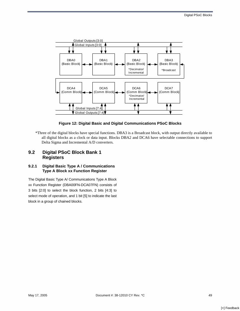
Digital PSoC Blocks
*Three of the digital blocks have special functions. DBA3 is a Broadcast block, with output directly available toall digital blocks as a clock or data input. Blocks DBA2 and DCA6 have selectable connections to supportDelta Sigma and Incremental A/D converters.
9.2 Digital PSoC Block Bank 1 Registers
9.2.1 Digital Basic Type A / Communications Type A Block xx Function Register
The Digital Basic Type A/ Communications Type A Block
xx Function Register (DBA00FN-DCA07FN) consists of
3 bits [2:0] to select the block function, 2 bits [4:3] to
select mode of operation, and 1 bit [5] to indicate the last
block in a group of chained blocks.
Figure 12: Digital Basic and Digital Communications PSoC Blocks
DBA0(Basic Block)
DBA1(Basic Block)
DBA2(Basic Block)
DBA3(Basic Block)
DCA4(Comm Block)
DCA5(Comm Block)
DCA6(Comm Block)
DCA7(Comm Block)
*Broadcast*Decimator/Incremental
*Decimator/Incremental
Global Inputs [3:0]Global Outputs [3:0]
Global Inputs [7:4]Global Outputs [7:4]
May 17, 2005 Document #: 38-12010 CY Rev. *C 49
[+] Feedback

CY8C25122/CY8C26233/CY8C26443/CY8C26643 Device Family Data Sheet
Digital Basic Type A Block 00 Function Register (DBA00FN, Address = Bank 1, 20h) Digital Basic Type A Block 01 Function Register (DBA01FN, Address = Bank 1, 24h)Digital Basic Type A Block 02 Function Register (DBA02FN, Address = Bank 1, 28h)Digital Basic Type A Block 03 Function Register (DBA03FN, Address = Bank 1, 2Ch)Digital Communications Type A Block 04 Function Register (DCA04FN, Address = Bank 1, 30h)
Table 47: Digital Basic Type A/ Communications Type A Block xx Function Register
Bit # 7 6 5 4 3 2 1 0
POR 0 0 0 0 0 0 0 0
Read/Write RW RW RW RW RW RW RW RW
Bit Name Reserved Reserved End Mode 1 Mode 0 Function [2] Function [1] Function [0]
Bit 7: ReservedBit 6: Reserved
Bit 5: End0 = PSoC block is not the end of a chained function (End should not be set to 0 in block DCA07)1 = PSoC block is the end of a chained function, or is an unchained PSoC block
Bit 4: Mode 1 The definition of the Mode [1] bit depends on the block function selectedTimer: The Mode [1] bit signifies the Compare Type0 = Less Than or Equal 1 = Less ThanCounter: The Mode [1] bit signifies the Compare Type0 = Less Than or Equal 1 = Less ThanCRC/PRS: The Mode [1] bit is unused in this functionDeadband: The Mode [1] bit is unused in this functionUART: The Mode[1] bit signifies the Interrupt Type (Transmitter only)0 = Transmit: Interrupt on TX_Reg Empty1 = Transmit: Interrupt on TX CompleteSPI: The Mode[1] bit signifies the Interrupt Type0 = Master: Interrupt on TX Reg Empty, Slave: Interrupt on RX Reg Full1 = Master: Interrupt on SPI Complete, Slave: Interrupt on SPI Complete
Bit 3: Mode 0 The definition of the Mode [0] bit depends on the block function selectedTimer: The Mode [0] bit signifies Interrupt Type 0 = Terminal Count 1 = Compare TrueCounter: The Mode [0] bit signifies Interrupt Type 0 = Terminal Count 1 = Compare TrueCRC/PRS: The Mode [0] bit is unused in this functionDeadband: The Mode [0] bit is unused in this functionUART: The Mode [0] bit signifies the Direction0 = Receive 1 = TransmitSPI: The Mode [0] bit signifies the Type0 = Master 1 = Slave
Bit [2:0]: Function [2:0] The Function [2:0] bits select the block function which determines the basic hardware configuration0 0 0 = Timer (chainable)0 0 1 = Counter (chainable)0 1 0 = CRC/PRS (Cyclical Redundancy Checker or Pseudo Random Sequencer) (chainable)0 1 1 = Reserved1 0 0 = Deadband for Pulse Width Modulator1 0 1 = UART (function only available on DCA type blocks)1 1 0 = SPI (function only available on DCA type blocks)1 1 1 = Reserved
50 Document #: 38-12010 CY Rev. *C May 17, 2005
[+] Feedback

Digital PSoC Blocks
Digital Communications Type A Block 05 Function Register (DCA05FN, Address = Bank 1, 34h)Digital Communications Type A Block 06 Function Register (DCA06FN, Address = Bank 1, 38h)Digital Communications Type A Block 07 Function Register (DCA07FN, Address = Bank 1, 3Ch)
9.2.2 Digital Basic Type A / Communications Type A Block xx Input Register
The Digital Basic Type A / Communications Type A Block
xx Input Register (DBA00IN-DCA07IN) consists of 4 bits
[3:0] to select the block input clock and 4 bits [7:4] to
select the primary data/enable input. The actual usage of
the input data/enable is function dependent.
Digital Basic Type A Block 00 Input Register (DBA00IN, Address = Bank 1, 21h)Digital Basic Type A Block 01 Input Register (DBA01IN, Address = Bank 1, 25h)Digital Basic Type A Block 02 Input Register (DBA02IN, Address = Bank 1, 29h)Digital Basic Type A Block 03 Input Register (DBA03IN, Address = Bank 1, 2Dh)Digital Communications Type A Block 04 Input Register (DCA04IN, Address = Bank 1, 31h)Digital Communications Type A Block 05 Input Register (DCA05IN, Address = Bank 1, 35h)
Table 48: Digital Basic Type A / Communications Type A Block xx Input Register
Bit # 7 6 5 4 3 2 1 0
POR 0 0 0 0 0 0 0 0
Read/Write RW RW RW RW RW RW RW RW
Bit Name Data [3] Data [2] Data [1] Data [0] Clock [3] Clock [2] Clock [1] Clock [0]
Bit [7:4]: Data [3:0] Data Enable Source Select0 0 0 0 = Data = 0 0 0 0 1 = Data = 1 0 0 1 0 = Digital Block 03 0 0 1 1 = Chain Function to Previous Block 0 1 0 0 = Analog Column Comparator 0 0 1 0 1 = Analog Column Comparator 1 0 1 1 0 = Analog Column Comparator 2 0 1 1 1 = Analog Column Comparator 3 1 0 0 0 = Global Output[0] (for Digital Blocks 00 to 03) or Global Output[4] (for Digital Blocks 04 to 07)1 0 0 1 = Global Output[1] (for Digital Blocks 00 to 03) or Global Output[5] (for Digital Blocks 04 to 07)1 0 1 0 = Global Output[2] (for Digital Blocks 00 to 03) or Global Output[6] (for Digital Blocks 04 to 07)1 0 1 1 = Global Output[3] (for Digital Blocks 00 to 03) or Global Output[7] (for Digital Blocks 04 to 07)1 1 0 0 = Global Input[0] (for Digital Blocks 00 to 03) or Global Input[4] (for Digital Blocks 04 to 07)1 1 0 1 = Global Input[1] (for Digital Blocks 00 to 03) or Global Input[5] (for Digital Blocks 04 to 07)1 1 1 0 = Global Input[2] (for Digital Blocks 00 to 03) or Global Input[6] (for Digital Blocks 04 to 07)1 1 1 1 = Global Input[3] (for Digital Blocks 00 to 03) or Global Input[7] (for Digital Blocks 04 to 07)
Bit [3:0]: Clock [3:0] Clock Source Select 0 0 0 0 = Clock Disabled0 0 0 1 = Global Output[4] (for Digital Blocks 00 to 03) or Global Output[0] (for Digital Blocks 04 to 07)0 0 1 0 = Digital Block 03 (Primary Output)0 0 1 1 = Previous Digital PSoC block (Primary Output)0 1 0 0 = 48M 0 1 0 1 = 24V1 0 1 1 0 = 24V2 0 1 1 1 = 32k 1 0 0 0 = Global Output[0] (for Digital Blocks 00 to 03) or Global Output[4] (for Digital Blocks 04 to 07)1 0 0 1 = Global Output[1] (for Digital Blocks 00 to 03) or Global Output[5] (for Digital Blocks 04 to 07)1 0 1 0 = Global Output[2] (for Digital Blocks 00 to 03) or Global Output[6] (for Digital Blocks 04 to 07)1 0 1 1 = Global Output[3] (for Digital Blocks 00 to 03) or Global Output[7] (for Digital Blocks 04 to 07)1 1 0 0 = Global Input[0] (for Digital Blocks 00 to 03) or Global Input[4] (for Digital Blocks 04 to 07)1 1 0 1 = Global Input[1] (for Digital Blocks 00 to 03) or Global Input[5] (for Digital Blocks 04 to 07)1 1 1 0 = Global Input[2] (for Digital Blocks 00 to 03) or Global Input[6] (for Digital Blocks 04 to 07)1 1 1 1 = Global Input[3] (for Digital Blocks 00 to 03) or Global Input[7] (for Digital Blocks 04 to 07)
May 17, 2005 Document #: 38-12010 CY Rev. *C 51
[+] Feedback

CY8C25122/CY8C26233/CY8C26443/CY8C26643 Device Family Data Sheet
Digital Communications Type A Block 06 Input Register (DCA06IN, Address = Bank 1, 39h)Digital Communications Type A Block 07 Input Register (DCA07IN, Address = Bank 1, 3Dh)
The Data/Enable source select [3:0] bits select between
multiple inputs to the Digital PSoC Blocks. These inputs
serve as Clock Enables or Data Input depending on the
Digital PSoC Block’s programmed function. If “Chain
Function to Previous” data input is selected for Data/
Enable then the selected Digital PSoC block receives its
Data, Enable, Zero Detect, and all chaining information
from the previous digital PSoC block. The data inputs
that are selected from the GPIO pins (through the Global
Input Bus) are synchronized to the 24 MHz clock. The
following table shows the function dependent meaning of
the data input.
The Clock[3:0] bits select multiple sources for the clock
for each digital PSoC block. The sources for each digital
PSoC block clock are selected from the Global Input
Bus, System Clocks, and other neighboring digital PSoC
blocks. As shown in the table, Digital PSoC Blocks 0-3
can interface to Global I/Os 00-03, and Digital PSoC
block 04-07 can interface to Global I/Os 4-7. It is impor-
tant to note that clock inputs selected from the GPIO pins
(through the Global Input Bus) are not synchronized.
This may cause indeterminate results if the CPU reads a
block register as it is changing in response to an external
clock. CPU reads must be manually synchronized, either
through the block interrupt, or through a multiple read
and voting scheme.
9.2.3 Digital Basic Type A / Communications Type A Block xx Output Register
The digital PSoC block’s outputs can be selected to drive
associated Global Output Bus signals via the Output
Select bits. In addition, the output drive can be selec-
tively enabled in this register. The SPI Slave has an aux-
iliary input which is also controlled by selections in this
register.
Table 49: Digital Function Data Input Definitions
Function Data Input
Timer Positive Edge Capture
Counter Count Enable (Active High)
CRC Data Input
PRS N/A
Deadband Kill Signal (Active High)
TX UART N/A
RX UART RX Data In
SPI Master MISO (Master In/Slave Out)
SPI Slave MOSI (Master Out/Slave In)
52 Document #: 38-12010 CY Rev. *C May 17, 2005
[+] Feedback

Digital PSoC Blocks
Digital Basic Type A Block 00 Output Register (DBA00OU, Address = Bank 1, 22h)Digital Basic Type A Block 01 Output Register (DBA01OU, Address = Bank 1, 26h)Digital Basic Type A Block 02 Output Register (DBA02OU, Address = Bank 1, 2Ah)Digital Basic Type A Block 03 Output Register (DBA03OU, Address = Bank 1, 2Eh)Digital Communications Type A Block 04 Output Register (DCA04OU, Address = Bank 1, 32h)Digital Communications Type A Block 05 Output Register (DCA05OU, Address = Bank 1, 36h)Digital Communications Type A Block 06 Output Register (DCA06OU, Address = Bank 1, 3Ah)Digital Communications Type A Block 07 Output Register (DCA07OU, Address = Bank 1, 3Eh)
The Primary Output is the source for “Previous Digital PSoC Block” or “Digital Block 03,” selections for the “Clock
Source Select” in the Digital Basic Type A/Communications Type A Block xx Input Register (Table 48 on page 51).
A digital PSoC block may have 0, 1, or 2 outputs depending on its function, as shown in the following table:
Table 50: Digital Basic Type A / Communications Type A Block xx Output Register
Bit # 7 6 5 4 3 2 1 0
POR 0 0 0 0 0 0 0 0Read/Write RW RW RW RW RW RW RW RW
Bit Name Reserved ReservedAUX Out Enable
AUX IO Sel [1]
AUX IO Sel [0]
Out Enable
Out Sel [1]
Out Sel [0]
Bit 7: ReservedBit 6: Reserved
Bit 5: AUX Out Enable0 = Disable Auxiliary Output1 = Enable Auxiliary Output (function dependent)
Bit [4:3]: AUX IO Sel [1:0] Function-dependent selection of auxiliary input or output0 0 = Drive Global Output[0] (for Digital Blocks 00 to 03) or
Input from Global Input[4] or Drive Global Output [4] (for Digital Blocks 04 to 07)0 1 = Drive Global Output[1] (for Digital Blocks 00 to 03) or
Input from Global Input[5] or Drive Global Output[5] (for Digital Blocks 04 to 07)1 0 = Drive Global Output[2] (for Digital Blocks 00 to 03) or
Input from Global Input[6] or Drive Global Output[6] (for Digital Blocks 04 to 07)1 1 = Drive Global Output[3] (for Digital Blocks 00 to 03) or
Input from Global Input[7] or Drive Global Output[7] (for Digital Blocks 04 to 07)
Bit 2: Out Enable0 = Disable Primary Output1 = Enable Primary Output (function dependant)
Bit [1:0]: Out Sel [1:0] Primary Output0 0 = Drive Global Output[0] (for Digital Blocks 00 to 03) or Drive Global Output[4] (for Digital Blocks 04 to 07)0 1 = Drive Global Output[1] (for Digital Blocks 00 to 03) or Drive Global Output[5] (for Digital Blocks 04 to 07)1 0 = Drive Global Output[2] (for Digital Blocks 00 to 03) or Drive Global Output[6] (for Digital Blocks 04 to 07)1 1 = Drive Global Output[3] (for Digital Blocks 00 to 03) or Drive Global Output[7] (for Digital Blocks 04 to 07)
May 17, 2005 Document #: 38-12010 CY Rev. *C 53
[+] Feedback

CY8C25122/CY8C26233/CY8C26443/CY8C26643 Device Family Data Sheet
9.3 Digital PSoC Block Bank 0 Registers
There are four user registers within each digital PSoC
block: three data registers, and one status/control regis-
ter. The three data registers are DR0, which is a shifter/
counter, and DR1 and DR2 registers, which contain data
used during the operation. The status/control register
(CR0) contains an enable bit that is used for all configu-
rations. In addition, it contains function-specific status
and control, which is outlined below.
9.3.1 Digital Basic Type A / Communications Type A Block xx Data Register 0,1,2
Digital Basic Type A Block 00 Data Register 0 (DBA00DR0, Address = Bank 0, 20h) Digital Basic Type A Block 00 Data Register 1 (DBA00DR1, Address = Bank 0, 21h) Digital Basic Type A Block 00 Data Register 2 (DBA00DR2, Address = Bank 0, 22h) Digital Basic Type A Block 01 Data Register 0 (DBA01DR0, Address = Bank 0, 24h)Digital Basic Type A Block 01 Data Register 1 (DBA01DR1, Address = Bank 0, 25h)Digital Basic Type A Block 01 Data Register 2 (DBA01DR2, Address = Bank 0, 26h)Digital Basic Type A Block 02 Data Register 0 (DBA02DR0, Address = Bank 0, 28h)Digital Basic Type A Block 02 Data Register 1 (DBA02DR1, Address = Bank 0, 29h)Digital Basic Type A Block 02 Data Register 2 (DBA02DR2, Address = Bank 0, 2Ah)Digital Basic Type A Block 03 Data Register 0 (DBA03DR0, Address = Bank 0, 2Ch)Digital Basic Type A Block 03 Data Register 1 (DBA03DR1, Address = Bank 0, 2Dh)Digital Basic Type A Block 03 Data Register 2 (DBA03DR2, Address = Bank 0, 2Eh)Digital Communications Type A Block 04 Data Register 0 (DCA04DR0, Address = Bank 0, 30h)Digital Communications Type A Block 04 Data Register 1 (DCA04DR1, Address = Bank 0, 31h)Digital Communications Type A Block 04 Data Register 2 (DCA04DR2, Address = Bank 0, 32h)Digital Communications Type A Block 05 Data Register 0 (DCA05DR0, Address = Bank 0, 34h)Digital Communications Type A Block 05 Data Register 1 (DCA05DR1, Address = Bank 0, 35h)Digital Communications Type A Block 05 Data Register 2 (DCA05DR2, Address = Bank 0, 36h)Digital Communications Type A Block 06 Data Register 0 (DCA06DR0, Address = Bank 0, 38h)Digital Communications Type A Block 06 Data Register 1 (DCA06DR1, Address = Bank 0, 39h)
Table 51: Digital Function Outputs
Function Primary Output Auxiliary Output Auxiliary Input
Timer Terminal Count Compare True N/A
Counter Compare True Terminal Count N/A
CRC N/A Compare True N/A
PRS Serial Data Compare True N/A
Deadband F0 F1 N/A
TX UART TX Data Out N/A N/A
RX UART N/A N/A N/A
SPI Master MOSI SCLK N/A
SPI Slave MISO N/A SS_
Table 52: Digital Basic Type A / Communications Type A Block xx Data Register 0,1,2
Bit # 7 6 5 4 3 2 1 0
POR 0 0 0 0 0 0 0 0
Read/Write VF1
1. Varies by function/User Module selection. (See Table 53 on page 55.)
VF1 VF1 VF1 VF1 VF1 VF1 VF1
Bit Name Data [7] Data [6] Data [5] Data [4] Data [3] Data [2] Data [1] Data [0]
Bit [7:0]: Data [7:0]
54 Document #: 38-12010 CY Rev. *C May 17, 2005
[+] Feedback

Digital PSoC Blocks
Digital Communications Type A Block 06 Data Register 2 (DCA06DR2, Address = Bank 0, 3Ah)Digital Communications Type A Block 07 Data Register 0 (DCA07DR0, Address = Bank 0, 3Ch)Digital Communications Type A Block 07 Data Register 1 (DCA07DR1, Address = Bank 0, 3Dh)Digital Communications Type A Block 07 Data Register 2 (DCA07DR2, Address = Bank 0, 3Eh)
9.3.2 Digital Basic Type A / Communications Type A Block xx Control Register 0
Digital Basic Type A Block 00 Control Register 0 (DBA00CR0, Address = Bank 0, 23h)Digital Basic Type A Block 01 Control Register 0 (DBA01CR0, Address = Bank 0, 27h)Digital Basic Type A Block 02 Control Register 0 (DBA02CR0, Address = Bank 0, 2Bh)Digital Basic Type A Block 03 Control Register 0 (DBA03CR0, Address = Bank 0, 2Fh)Digital Communications Type A Block 04 Control Register 0 (DCA04CR0, Address = Bank 0, 33h)Digital Communications Type A Block 05 Control Register 0 (DCA05CR0, Address = Bank 0, 37h)Digital Communications Type A Block 06 Control Register 0 (DCA06CR0, Address = Bank 0, 3Bh)Digital Communications Type A Block 07 Control Register 0 (DCA07CR0, Address = Bank 0, 3Fh)
Table 53: R/W Variations per User Module Selection
Function DR0 R/W DR1 R/W DR2 R/W
Timer Count R1 Period Value W Capture Value RW
Counter Count R1 Period Value W Compare Value RW
CRC Current Value/CRC Residue R1 Polynomial Mask Value W Seed Value RW
PRS Current Value R1 Polynomial Mask Value W Seed Value RW
Deadband Count R1 Period Value W Not Used RW
RX UART Shifter NA Not Used NA Data Register R
TX UART Shifter NA Data Register W Not Used NA
SPI Shifter NA TX Data Register RX Data Register R
1. Each time the register is read, its value is written to the DR2 register.
Table 54: Digital Basic Type A / Communications Type A Block xx Control Register 0
Bit # 7 6 5 4 3 2 1 0
POR 0 0 0 0 0 0 0 0
Read/Write VF1
1. Varies by function.
VF1 VF1 VF1 VF1 VF1 VF1 VF1
Bit Name Data [7] Data [6] Data [5] Data [4] Data [3] Data [2] Data [1] Data [0]
Bit [7:0]: Data [7:0]
May 17, 2005 Document #: 38-12010 CY Rev. *C 55
[+] Feedback
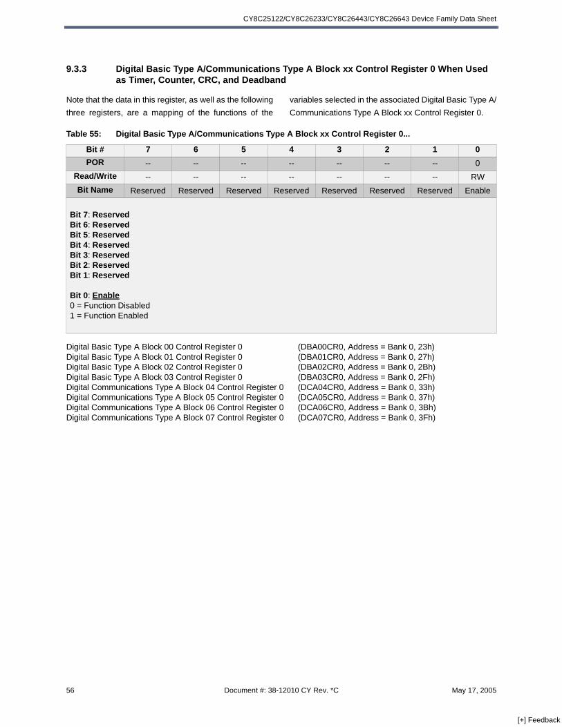
CY8C25122/CY8C26233/CY8C26443/CY8C26643 Device Family Data Sheet
9.3.3 Digital Basic Type A/Communications Type A Block xx Control Register 0 When Used as Timer, Counter, CRC, and Deadband
Note that the data in this register, as well as the following
three registers, are a mapping of the functions of the
variables selected in the associated Digital Basic Type A/
Communications Type A Block xx Control Register 0.
Digital Basic Type A Block 00 Control Register 0 (DBA00CR0, Address = Bank 0, 23h)Digital Basic Type A Block 01 Control Register 0 (DBA01CR0, Address = Bank 0, 27h)Digital Basic Type A Block 02 Control Register 0 (DBA02CR0, Address = Bank 0, 2Bh)Digital Basic Type A Block 03 Control Register 0 (DBA03CR0, Address = Bank 0, 2Fh)Digital Communications Type A Block 04 Control Register 0 (DCA04CR0, Address = Bank 0, 33h)Digital Communications Type A Block 05 Control Register 0 (DCA05CR0, Address = Bank 0, 37h)Digital Communications Type A Block 06 Control Register 0 (DCA06CR0, Address = Bank 0, 3Bh)Digital Communications Type A Block 07 Control Register 0 (DCA07CR0, Address = Bank 0, 3Fh)
Table 55: Digital Basic Type A/Communications Type A Block xx Control Register 0...
Bit # 7 6 5 4 3 2 1 0
POR -- -- -- -- -- -- -- 0
Read/Write -- -- -- -- -- -- -- RW
Bit Name Reserved Reserved Reserved Reserved Reserved Reserved Reserved Enable
Bit 7: ReservedBit 6: ReservedBit 5: ReservedBit 4: ReservedBit 3: ReservedBit 2: ReservedBit 1: Reserved
Bit 0: Enable0 = Function Disabled1 = Function Enabled
56 Document #: 38-12010 CY Rev. *C May 17, 2005
[+] Feedback
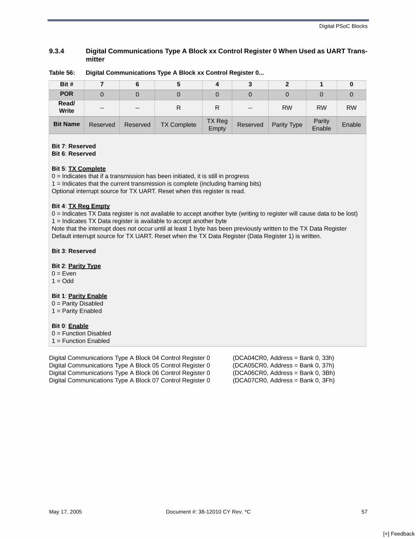
Digital PSoC Blocks
9.3.4 Digital Communications Type A Block xx Control Register 0 When Used as UART Trans-mitter
Digital Communications Type A Block 04 Control Register 0 (DCA04CR0, Address = Bank 0, 33h)Digital Communications Type A Block 05 Control Register 0 (DCA05CR0, Address = Bank 0, 37h)Digital Communications Type A Block 06 Control Register 0 (DCA06CR0, Address = Bank 0, 3Bh)Digital Communications Type A Block 07 Control Register 0 (DCA07CR0, Address = Bank 0, 3Fh)
Table 56: Digital Communications Type A Block xx Control Register 0...
Bit # 7 6 5 4 3 2 1 0
POR 0 0 0 0 0 0 0 0Read/Write -- -- R R -- RW RW RW
Bit Name Reserved Reserved TX CompleteTX Reg Empty
Reserved Parity TypeParity Enable
Enable
Bit 7: ReservedBit 6: Reserved
Bit 5: TX Complete0 = Indicates that if a transmission has been initiated, it is still in progress1 = Indicates that the current transmission is complete (including framing bits)Optional interrupt source for TX UART. Reset when this register is read.
Bit 4: TX Reg Empty0 = Indicates TX Data register is not available to accept another byte (writing to register will cause data to be lost)1 = Indicates TX Data register is available to accept another byte Note that the interrupt does not occur until at least 1 byte has been previously written to the TX Data RegisterDefault interrupt source for TX UART. Reset when the TX Data Register (Data Register 1) is written.
Bit 3: Reserved
Bit 2: Parity Type0 = Even1 = Odd
Bit 1: Parity Enable0 = Parity Disabled1 = Parity Enabled
Bit 0: Enable0 = Function Disabled1 = Function Enabled
May 17, 2005 Document #: 38-12010 CY Rev. *C 57
[+] Feedback
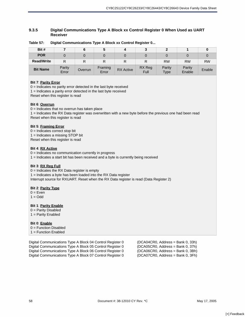
CY8C25122/CY8C26233/CY8C26443/CY8C26643 Device Family Data Sheet
9.3.5 Digital Communications Type A Block xx Control Register 0 When Used as UART Receiver
Digital Communications Type A Block 04 Control Register 0 (DCA04CR0, Address = Bank 0, 33h)Digital Communications Type A Block 05 Control Register 0 (DCA05CR0, Address = Bank 0, 37h)Digital Communications Type A Block 06 Control Register 0 (DCA06CR0, Address = Bank 0, 3Bh)Digital Communications Type A Block 07 Control Register 0 (DCA07CR0, Address = Bank 0, 3Fh)
Table 57: Digital Communications Type A Block xx Control Register 0...
Bit # 7 6 5 4 3 2 1 0
POR 0 0 0 0 0 0 0 0
Read/Write R R R R R RW RW RW
Bit Name Parity Error
OverrunFraming
ErrorRX Active
RX Reg Full
Parity Type
Parity Enable
Enable
Bit 7: Parity Error0 = Indicates no parity error detected in the last byte received1 = Indicates a parity error detected in the last byte received Reset when this register is read
Bit 6: Overrun0 = Indicates that no overrun has taken place 1 = Indicates the RX Data register was overwritten with a new byte before the previous one had been read Reset when this register is read
Bit 5: Framing Error0 = Indicates correct stop bit1 = Indicates a missing STOP bit Reset when this register is read
Bit 4: RX Active0 = Indicates no communication currently in progress1 = Indicates a start bit has been received and a byte is currently being received
Bit 3: RX Reg Full0 = Indicates the RX Data register is empty1 = Indicates a byte has been loaded into the RX Data register Interrupt source for RXUART. Reset when the RX Data register is read (Data Register 2)
Bit 2: Parity Type0 = Even1 = Odd
Bit 1: Parity Enable0 = Parity Disabled1 = Parity Enabled
Bit 0: Enable0 = Function Disabled1 = Function Enabled
58 Document #: 38-12010 CY Rev. *C May 17, 2005
[+] Feedback

Digital PSoC Blocks
9.3.6 Digital Communications Type A Block xx Control Register 0 When Used as SPI Trans-ceiver
Digital Communications Type A Block 04 Control Register 0 (DCA04CR0, Address = Bank 0, 33h)Digital Communications Type A Block 05 Control Register 0 (DCA05CR0, Address = Bank 0, 37h)Digital Communications Type A Block 06 Control Register 0 (DCA06CR0, Address = Bank 0, 3Bh)Digital Communications Type A Block 07 Control Register 0 (DCA07CR0, Address = Bank 0, 3Fh)
Table 58: Digital Communications Type A Block xx Control Register 0...
Bit # 7 6 5 4 3 2 1 0
POR 0 0 0 0 0 0 0 0Read/Write RW R R R R RW RW RW
Bit Name LSB First Overrun SPI CompleteTX Reg Empty
RX Reg Full
Clock Phase
Clock Polarity
Enable
Bit 7: LSB First0 = MSB First1 = LSB First
Bit 6: Overrun0 = Indicates that no overrun has taken place 1 = Indicates the RX Data register was overwritten with a new byte before the previous one had been read Reset when this register is read
Bit 5: SPI Complete0 = Indicates the byte is in process of shifting out1 = Indicates the byte has been shifted out (reset when register is read)Optional interrupt source for both SPI Master and SPI Slave. Reset when this register is read
Bit 4: TX Reg Empty0 = Indicates the TX Data register is not available to accept another byte1 = Indicates the TX Data register is available to accept another byteDefault interrupt source for SPI Master. Reset when the TX Data Register (Data Register 1) is written.
Bit 3: RX Reg Full0 = Indicates the RX Data register is empty1 = Indicates a byte has been loaded into the RX Data registerDefault interrupt source for SPI Slave. Reset when the RX Data Register (Data Register 2) is read
Bit 2: Clock Phase0 = Data changes on leading edge and is latched on trailing edge1 = Data is latched on leading edge and is changed on trailing edge
Bit 1: Clock Polarity0 = Non-inverted (clock idle state is low)1 = Inverted (clock idle state is high)
Bit 0: Enable0 = Function Disabled1 = Function Enabled
May 17, 2005 Document #: 38-12010 CY Rev. *C 59
[+] Feedback
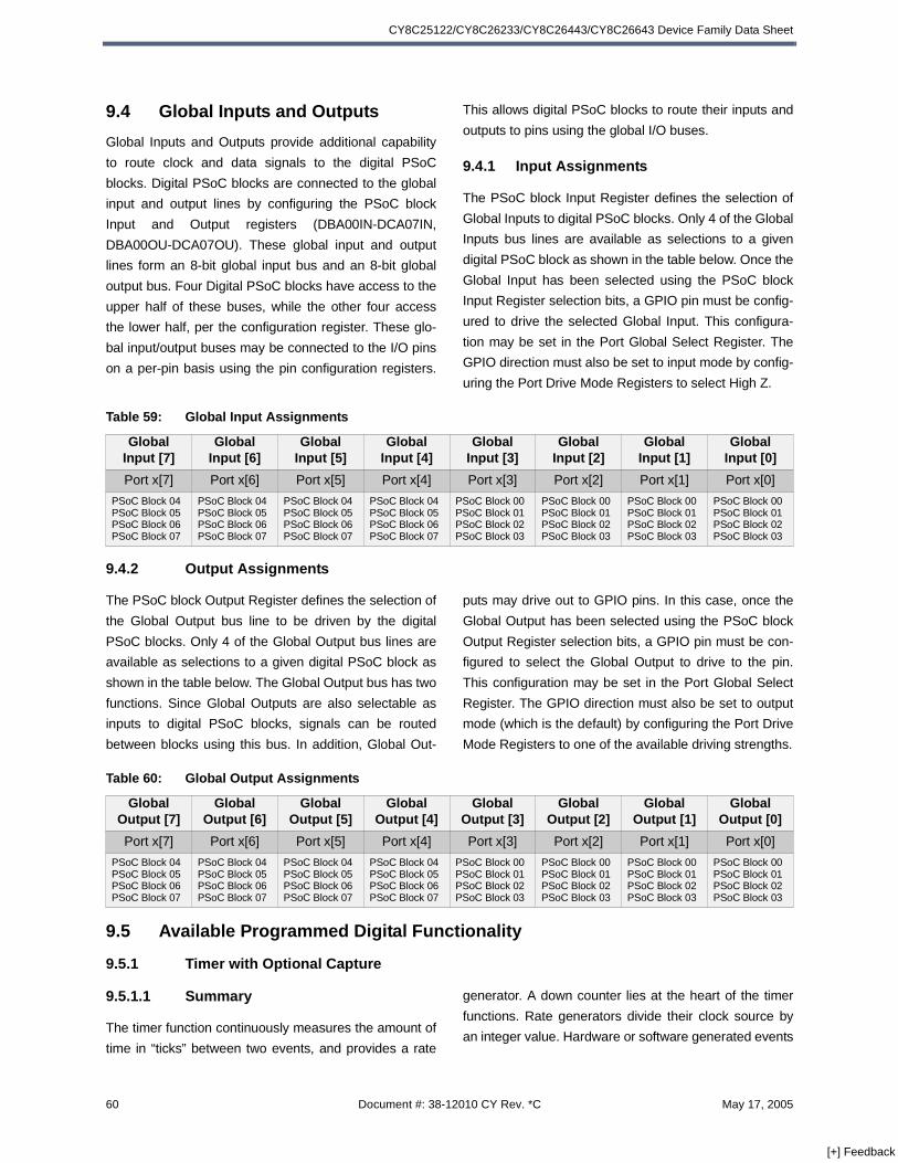
CY8C25122/CY8C26233/CY8C26443/CY8C26643 Device Family Data Sheet
9.4 Global Inputs and Outputs
Global Inputs and Outputs provide additional capability
to route clock and data signals to the digital PSoC
blocks. Digital PSoC blocks are connected to the global
input and output lines by configuring the PSoC block
Input and Output registers (DBA00IN-DCA07IN,
DBA00OU-DCA07OU). These global input and output
lines form an 8-bit global input bus and an 8-bit global
output bus. Four Digital PSoC blocks have access to the
upper half of these buses, while the other four access
the lower half, per the configuration register. These glo-
bal input/output buses may be connected to the I/O pins
on a per-pin basis using the pin configuration registers.
This allows digital PSoC blocks to route their inputs and
outputs to pins using the global I/O buses.
9.4.1 Input Assignments
The PSoC block Input Register defines the selection of
Global Inputs to digital PSoC blocks. Only 4 of the Global
Inputs bus lines are available as selections to a given
digital PSoC block as shown in the table below. Once the
Global Input has been selected using the PSoC block
Input Register selection bits, a GPIO pin must be config-
ured to drive the selected Global Input. This configura-
tion may be set in the Port Global Select Register. The
GPIO direction must also be set to input mode by config-
uring the Port Drive Mode Registers to select High Z.
9.4.2 Output Assignments
The PSoC block Output Register defines the selection of
the Global Output bus line to be driven by the digital
PSoC blocks. Only 4 of the Global Output bus lines are
available as selections to a given digital PSoC block as
shown in the table below. The Global Output bus has two
functions. Since Global Outputs are also selectable as
inputs to digital PSoC blocks, signals can be routed
between blocks using this bus. In addition, Global Out-
puts may drive out to GPIO pins. In this case, once the
Global Output has been selected using the PSoC block
Output Register selection bits, a GPIO pin must be con-
figured to select the Global Output to drive to the pin.
This configuration may be set in the Port Global Select
Register. The GPIO direction must also be set to output
mode (which is the default) by configuring the Port Drive
Mode Registers to one of the available driving strengths.
9.5 Available Programmed Digital Functionality
9.5.1 Timer with Optional Capture
9.5.1.1 Summary
The timer function continuously measures the amount of
time in “ticks” between two events, and provides a rate
generator. A down counter lies at the heart of the timer
functions. Rate generators divide their clock source by
an integer value. Hardware or software generated events
Table 59: Global Input Assignments
GlobalInput [7]
GlobalInput [6]
GlobalInput [5]
GlobalInput [4]
GlobalInput [3]
GlobalInput [2]
GlobalInput [1]
GlobalInput [0]
Port x[7] Port x[6] Port x[5] Port x[4] Port x[3] Port x[2] Port x[1] Port x[0]
PSoC Block 04PSoC Block 05PSoC Block 06PSoC Block 07
PSoC Block 04PSoC Block 05PSoC Block 06PSoC Block 07
PSoC Block 04PSoC Block 05PSoC Block 06PSoC Block 07
PSoC Block 04PSoC Block 05PSoC Block 06PSoC Block 07
PSoC Block 00PSoC Block 01PSoC Block 02PSoC Block 03
PSoC Block 00PSoC Block 01PSoC Block 02PSoC Block 03
PSoC Block 00PSoC Block 01PSoC Block 02PSoC Block 03
PSoC Block 00PSoC Block 01PSoC Block 02PSoC Block 03
Table 60: Global Output Assignments
Global Output [7]
GlobalOutput [6]
GlobalOutput [5]
GlobalOutput [4]
GlobalOutput [3]
GlobalOutput [2]
GlobalOutput [1]
GlobalOutput [0]
Port x[7] Port x[6] Port x[5] Port x[4] Port x[3] Port x[2] Port x[1] Port x[0]
PSoC Block 04PSoC Block 05PSoC Block 06PSoC Block 07
PSoC Block 04PSoC Block 05PSoC Block 06PSoC Block 07
PSoC Block 04PSoC Block 05PSoC Block 06PSoC Block 07
PSoC Block 04PSoC Block 05PSoC Block 06PSoC Block 07
PSoC Block 00PSoC Block 01PSoC Block 02PSoC Block 03
PSoC Block 00PSoC Block 01PSoC Block 02PSoC Block 03
PSoC Block 00PSoC Block 01PSoC Block 02PSoC Block 03
PSoC Block 00PSoC Block 01PSoC Block 02PSoC Block 03
60 Document #: 38-12010 CY Rev. *C May 17, 2005
[+] Feedback

Digital PSoC Blocks
trigger capture operations that permit calculation of
elapsed “ticks.” Timer-configured PSoC blocks may be
chained to arbitrary lengths in 8 bit increments.
9.5.1.2 Registers
Data Register 1 establishes the period or integer clock
division value. Data Register 0 holds the current state of
the down counter. If the function is disabled, writing a
period into Data Register 1, will automatically load Data
Register 0. It is also automatically reloaded on the clock
cycle after it reaches zero, the terminal count value.
When a capture event occurs, the current value of Data
Register 0 is transferred to Data Register 2. The cap-
tured value in Data Register 2 may then be read by the
CPU. In addition to the hardware capture input, A CPU
read of Data Register 0 generates a software capture
event. This read will return 0 as data. A subsequent read
of Data Register 2 will return the captured value. Control
Register 0 contains one bit to enable/disable the func-
tion.
9.5.1.3 Inputs
There are two inputs, the Source Clock and the Hard-
ware Capture signal. The down counter is decremented
on the rising-edge of the Source Clock. A hardware cap-
ture event is signaled by a rising edge of the Hardware
Capture signal. This is synchronized to the 24 MHz sys-
tem clock and the data is synchronously transferred to
Data Register 2. The Hardware Capture Signal is OR’ed
with a software capture signal that is generated when
Data Register 0 is read directly by the CPU. In order to
use the software capture mechanism, the Hardware
Capture signal input selection must be low. The multi-
plexers selecting these input sources are controlled by
the PSoC block Input Register (DBA00IN-DCA07IN).
9.5.1.4 Outputs
The Terminal Count signal is the primary output and it
exhibits a duty cycle that is the reciprocal of the period
value contained in Data Register 1. In other words, it is
high during the source clock cycle when the value in
Data Register 0 is zero and low otherwise. The Terminal
Count can be routed to additional analog or digital PSoC
blocks or via Global Output lines. The auxiliary output is
the Compare True signal. This output is high when the
current count is less than (or less than or equal to) the
value in Data Register 2 (compare type controlled by
Mode[1] in the PSoC block Function Register). The auxil-
iary output can be routed via Global Output lines. The
PSoC block Output Register (DBA00OU-DCA07OU)
controls output options.
9.5.1.5 Interrupts
Interrupts may be generated in either of two ways. First,
the PSoC block may optionally generate an interrupt on
the rising edge of Terminal Count or the rising edge of
the Compare True signal. The selection of interrupt
source is determined by the MODE[0] bit of the PSoC
block Function Register (DBA00FN-DCA07FN). The
MODE[1] bit controls whether the comparison operation
is “less than” or “less than or equal to.” If capture events
are disabled, Data Register 2 can be used to create a
periodic interrupt with a particular offset from the terminal
count.
9.5.1.6 Usage Notes
1. Constraints
Hardware/software synchronous capture is only available with a clocking rate of 24 MHz and below.
2. Software Capture
When a capture event occurs, all bytes in a multi-byte timer transfer simultaneously from the current count (Data Register 0) to the capture register (Data Register 2). To generate a software capture event, only the least significant Data Register 0 byte needs to be read by the CPU. This causes the same simul-taneous transfer as a hardware event.
3. Disabled State
When the Control Register Enable bit is set to ‘0’, the internal block clock is turned off. A write to Data Register 1 (Period) is loaded directly into Data Reg-ister 0 (Counter) to initialize or reset the count. All outputs are low and the block interrupt is held low. Disabling a timer does not affect the current count value and it may be read by the CPU. However, since hardware/software capture is disabled in this state, two reads are required to read each byte of a multi-byte register. One to transfer each Data Regis-ter 0 count value to the associated Data Register 2 capture register, then one to read the result in Data Register 2.
May 17, 2005 Document #: 38-12010 CY Rev. *C 61
[+] Feedback
CY8C25122/CY8C26233/CY8C26443/CY8C26643 Device Family Data Sheet
4. Capture vs. Compare
A capture event will overwrite Data Register 2. This is also the register that holds the compare value. Therefore, using the capture function may not be compatible with using the timer compare function.
9.5.2 Counter with Optional Compare (Pulse-Width) Output
9.5.2.1 Summary
Conceptually, a counter measures the number of events
between “ticks,” however, this distinction between
counter and timer blurs because both functions provide a
complete range of clock selections. The counter trades
the timer’s hardware capture for a clock gate or ”enable”
and provides a means of adjusting the duty cycle of its
output so that it can double as a pulse-width modulator.
A down counter lies at the heart of the counter function.
Counter-configured PSoC blocks may be chained to
arbitrary lengths in 8 bit increments.
In a Counter User Module, the data input is an enable for
counting. Normally, when the enable goes low, the
counter will hold the current count. However, if the
enable happens to go low in the same clock period as
Terminal Count (count of all 0's), one additional count will
occur that will reload the counter from the Period Regis-
ter. Once the counter is reloaded from the Period Regis-
ter, counting will stop.
9.5.2.2 Registers
Data Register 1 establishes the period of the counter.
Data Register 0 holds the current state of the down
counter. If the function is disabled, writing a period into
Data Register 1, will automatically load Data Register 0.
It is also automatically reloaded on the clock cycle after it
reaches zero, the terminal count value. The value in
Data Register 2 (compare value) is continually compared
to Data Register 0 (count value) to establish the output
pulse-width (duty cycle). Reading Data Register 0 to
obtain the current value of the down counter may occur
only when the function is disabled. When read, this
transfers the value from Data Register 0 to Data Register
2 and returns a 0 on the data bus. The value transferred
to Data Register 2 can then be directly read by the CPU.
However, reading the count value in this manner will
overwrite any previously written compare value in Data
Register 2. Control Register 0 contains one bit to
enable/disable the function.
9.5.2.3 Inputs
There are two primary inputs, the Source Clock and the
Enable signal. When the Enable signal is high, the down
counter is decremented on the rising-edge of the Source
Clock. The multiplexers selecting these inputs are con-
trolled by the PSoC block Input Register (DBA00IN-
DCA07IN).
9.5.2.4 Outputs
The counter function drives its primary output signal,
Compare True, high on the falling edge of the Source
Clock when the value in Data Register 0 is less (or less
than or equal to) the value in Data Register 2. The duty
cycle of the pulse-width modulator formed in this way is
the ratio of Data Register 2 (or Data Register 2 minus
one) to Data Register 1. The choice of compare opera-
tors is determined by the MODE[1] bit. The Compare
value can be routed to additional analog or digital PSoC
blocks or via Global Output lines The auxiliary output sig-
nal is the Terminal Count signal which can be routed via
Global Output lines. The PSoC block Output Register
(DBA00OU-DCA07OU) controls output options.
9.5.2.5 Interrupts
Interrupts may be generated in either of two ways. First,
the PSoC block may optionally generate an interrupt on
the rising edge of Terminal Count or the rising edge of
the Compare signal. The selection of interrupt source is
determined by the MODE[0] bit of the PSoC block Func-
tion Register (DBA00FN-DCA07FN). The MODE[1] bit
controls whether the comparison operation is “less than”
or “less than or equal to.”
9.5.2.6 Usage Notes
1. Enable Input
The enable input is synchronous and when low forces the counter into a ‘hold’ state. Outputs are unaffected by the state of the enable input. If an external source is selected as the enable input, it is synchronized to the 24 MHz clock.
62 Document #: 38-12010 CY Rev. *C May 17, 2005
[+] Feedback

Digital PSoC Blocks
2. Disabled State
When the Control Register Enable bit is set to ‘0’, the internal block clock is turned off. A write to Data Register 1 (Period) is loaded directly into Data Reg-ister 0 (Counter) to initialize or reset the count. All outputs are low and the block interrupt is held low. Disabling a counter does not affect the current count value and it may be read by the CPU. Two reads are required to read each byte of a multi-byte register. One to transfer each Data Register 0 count value to the associated Data Register 2 capture register, then one to read the result in Data Register 2.
3. Reading the Count Value
A CPU read of Data Register 0 (count value) will overwrite Data Register 2 (compare value). There-fore, when reading the current count, a previously written compare value will be overwritten.
4. Extra Count
In a Counter User Module, the data input is an enable for counting. Normally, when the enable goes low, the counter will hold the current count. However, if the enable happens to go low in the same clock period as Terminal Count (count of all 0's), one additional count will occur that will reload the counter from the Period Register. Once the counter is reloaded from the Period Register, count-ing will stop.
9.5.3 Deadband Generator
9.5.3.1 Summary
The Deadband function produces two output waveforms,
F0 and F1, with the same frequency as the input, but
“under-lapped” so they are never both high at the same
time. An 8-bit down counter controls the length of the
“dead time” during which both output signals are low.
When the deadband function detects a rising edge on
the input waveform, the F1 output signal goes low and
the counter decrements from its initial value to its termi-
nal count. When the down counter reaches zero, the F0
output signal goes high. The process reverses on the
falling edge of the input waveform so that after the same
dead time, F1 goes high until the input signal transitions
again. Dead-band generator PSoC blocks cannot be
chained to increase the width of the down counter
beyond 8 bits or 256 dead-time “ticks.”
9.5.3.2 Registers
Data Register 1 stores the count that controls the
elapsed dead time. Data Register 0 holds the current
state of the dead-time down counter. If the function is
disabled, writing a period into Data Register 1, will auto-
matically load Data Register 0 with the deadband period.
This period is automatically re-loaded into the counter on
each edge of the input signal. Data Register 2 is unused.
Control Register 0 contains one bit to enable/disable the
function.
9.5.3.3 Inputs
The input controls the period and duty cycle of the dead-
band generator outputs. This input is fixed to be derived
from the primary output of the previous block. If this sig-
nal is pulse-width modulated, i.e., if a PWM block is con-
figured as the previous block, the dead-band outputs will
be similarly modulated. The F0 output corresponds to
the duty cycle of the input (less the dead time) and F1 to
the duty cycle of the inverted input (again, less the dead
time). The clock input to the dead-band generator con-
trols the rate at which the down counter is decremented.
The primary data input is the “Kill” Signal. When this sig-
nal is asserted high, both F0 and F1 outputs will go low.
The multiplexers selecting these input are controlled by
the PSoC block Input Register (DBA00IN-DCA07IN).
9.5.3.4 Outputs
Both the F0 and F1 outputs can be driven onto the Glo-
bal Output bus. If the next PSoC block selects “Previous
PSoC block” for its clock input, it only “sees” the F0 out-
put of the dead-band function. The PSoC block Output
Register (DBA00OU-DCA07OU) controls output options.
9.5.3.5 Interrupts
The rising edge of the F0 signal provides the interrupt for
this block.
9.5.3.6 Usage Notes
1. Constraints
The dead time must not exceed the minimum of the input signal’s pulse-width high and pulse-width low time, less two CPU clocks. Dead time equals the period of the input clock times one plus the value written to Data Register 1.
May 17, 2005 Document #: 38-12010 CY Rev. *C 63
[+] Feedback

CY8C25122/CY8C26233/CY8C26443/CY8C26643 Device Family Data Sheet
2. Enabling
The data input to the Dead-Band function is hard-ware to the primary output of the previous block, which is typically programmed to be a PWM. The proper order for enabling these blocks (writing the Control Register 0) is PWM first, then Dead-Band.
3. Disabled State
When the Control Register Enable bit is set to ‘0’, the internal block clock is turned off. A write to Data Register 1 (Period) is loaded directly into Data Reg-ister 0 (Counter) to initialize or reset the dead-band time. All outputs are low and the block interrupt is held low.
4. Asserting the Kill Signal
When the Kill signal is asserted high, both outputs FO and F1 are held low. When the Kill signal is selected from an external source through a Global Input, it is synchronized to the 24 MHz clock and therefore has up to 42 ns of latency.
5. Negating the Kill Signal
The Kill signal may be negated at any time. How-ever, the output may be enabled at an arbitrary time with respect to the F0 and F1 generation. If exact timing is required when re-enabling the F0 and F1 outputs, the following procedure is recommended:
1.Kill is asserted.
2.Write to Control Register 0 to disable the block.
3.Write to Data Register 1 (Deadband time) to initialize the period.
4.Kill is eventually negated.
5.Write to Control Register 0 to enable the block.
9.5.4 PRS - Pseudo-Random Sequence Generator
9.5.4.1 Summary
The PRS function generates an output waveform corre-
sponding to a sequence of pseudo-random numbers. A
linear-feedback shift register generates the sequence
according to a user-specified polynomial. The width of
the numbers in the sequence is variable and the initial
value is determined by a user-defined “seed” value. PRS
PSoC blocks can be chained to increase the width of the
numbers and, hence, the length of the sequence. A
chain of N PSoC blocks can generate numbers from 2-
to 8N-bits wide and sequences of up to 28N-1 distinct val-
ues.
9.5.4.2 Registers
Data Register 0 implements a linear-feedback shift regis-
ter. Data Register 2 holds the “seed” value and when the
block is disabled, a write to Data Register 2 is loaded
directly into Data Register 0 (The block must be disabled
when writing this value). Data Register 1 specifies the
polynomial and width of the numbers in the sequence
(see 9.5.4.6).
9.5.4.3 Inputs
The clock input determines the rate at which the output
sequence is produced. The data input must be set to low
for the block to function as a PRS. The multiplexer for
selecting these inputs is controlled by the PSoC block
Input Register (DBA00IN-DCA07IN).
9.5.4.4 Outputs
The PRS function drives the output serial data stream
synchronous with the input clock. The output bits change
on the rising edge of the input clock. The output may be
driven on the Global Output bus or to the subsequent
digital PSoC block. The PSoC block Output Register
(DBA00OU-DCA07OU) controls output options.
9.5.4.5 Interrupts
The PRS function provides an interrupt based on the
Compare signal between Data Register 0 and Data Reg-
ister 2. Data Register 2 is initially loaded with the “seed”
value, and therefore a periodic interrupt will be gener-
ated when the PRS count matches the seed value.
64 Document #: 38-12010 CY Rev. *C May 17, 2005
[+] Feedback
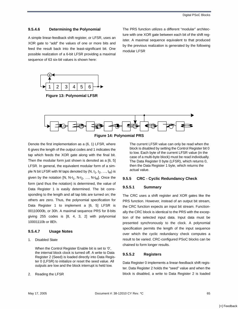
Digital PSoC Blocks
9.5.4.6 Determining the Polynomial
A simple linear-feedback shift register, or LFSR, uses an
XOR gate to “add” the values of one or more bits and
feed the result back into the least-significant bit. One
possible realization of a 6-bit LFSR providing a maximal
sequence of 63 six-bit values is shown here:
The PRS function utilizes a different “modular” architec-
ture with one XOR gate between each bit of the shift reg-
ister. A maximal sequence equivalent to that produced
by the previous realization is generated by the following
modular LFSR
Denote the first implementation as a (6, 1) LFSR, where
6 gives the length of the output codes and 1 indicates the
tap which feeds the XOR gate along with the final bit.
Then the modular form just shown is denoted as a [6, 5]
LFSR. In general, the equivalent modular form of a sim-
ple N bit LFSR with M taps denoted by (N, t1, t2, …, tM) is
given by the notation [N, N-t1, N-t2, …, N-tM]. Once the
form (and thus the notation) is determined, the value of
Data Register 1 is easily determined. The bit corre-
sponding to the length and all tap bits are turned on; the
others are zero. Thus, the polynomial specification for
Data Register 1 to implement a [6, 5] LFSR is
00110000b, or 30h. A maximal sequence PRS for 8-bits
giving 255 codes is [8, 4, 3, 2] with polynomial
10001110b or 8Eh.
9.5.4.7 Usage Notes
1. Disabled State
When the Control Register Enable bit is set to ‘0’, the internal block clock is turned off. A write to Data Register 2 (Seed) is loaded directly into Data Regis-ter 0 (LFSR) to initialize or reset the seed value. All outputs are low and the block interrupt is held low.
2. Reading the LFSR
The current LFSR value can only be read when the block is disabled by setting the Control Register bit 0 to low. Each byte of the current LFSR value (in the case of a multi-byte block) must be read individually. The Data Register 0 byte (LFSR), which returns 0, then the Data Register 1 byte, which returns the actual value.
9.5.5 CRC - Cyclic Redundancy Check
9.5.5.1 Summary
The CRC uses a shift register and XOR gates like the
PRS function. However, instead of an output bit stream,
the CRC function expects an input bit stream. Function-
ally the CRC block is identical to the PRS with the excep-
tion of the selected input data. Input data must be
presented synchronously to the clock. A polynomial
specification permits the length of the input sequence
over which the cyclic redundancy check computes a
result to be varied. CRC-configured PSoC blocks can be
chained to form longer results.
9.5.5.2 Registers
Data Register 0 implements a linear-feedback shift regis-
ter. Data Register 2 holds the “seed” value and when the
block is disabled, a write to Data Register 2 is loaded
Figure 13: Polynomial LFSR
1 2 3 4 5 6
+
Figure 14: Polynomial PRS
B+++++++1 2 345 6 7 8
May 17, 2005 Document #: 38-12010 CY Rev. *C 65
[+] Feedback
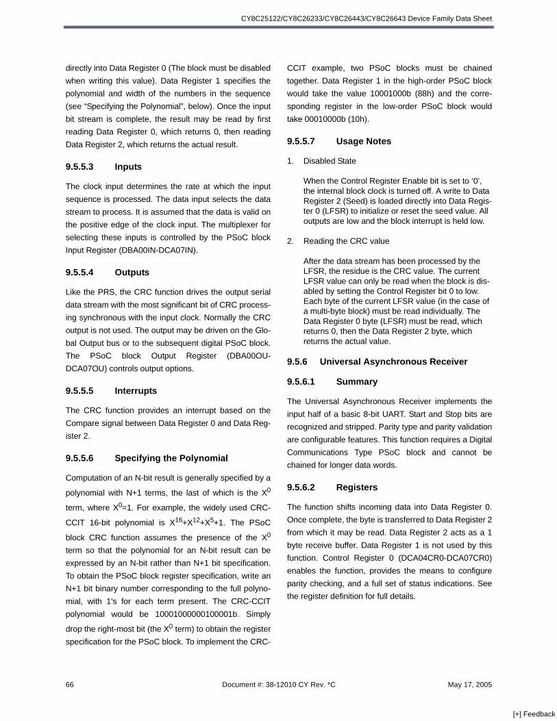
CY8C25122/CY8C26233/CY8C26443/CY8C26643 Device Family Data Sheet
directly into Data Register 0 (The block must be disabled
when writing this value). Data Register 1 specifies the
polynomial and width of the numbers in the sequence
(see “Specifying the Polynomial”, below). Once the input
bit stream is complete, the result may be read by first
reading Data Register 0, which returns 0, then reading
Data Register 2, which returns the actual result.
9.5.5.3 Inputs
The clock input determines the rate at which the input
sequence is processed. The data input selects the data
stream to process. It is assumed that the data is valid on
the positive edge of the clock input. The multiplexer for
selecting these inputs is controlled by the PSoC block
Input Register (DBA00IN-DCA07IN).
9.5.5.4 Outputs
Like the PRS, the CRC function drives the output serial
data stream with the most significant bit of CRC process-
ing synchronous with the input clock. Normally the CRC
output is not used. The output may be driven on the Glo-
bal Output bus or to the subsequent digital PSoC block.
The PSoC block Output Register (DBA00OU-
DCA07OU) controls output options.
9.5.5.5 Interrupts
The CRC function provides an interrupt based on the
Compare signal between Data Register 0 and Data Reg-
ister 2.
9.5.5.6 Specifying the Polynomial
Computation of an N-bit result is generally specified by a
polynomial with N+1 terms, the last of which is the X0
term, where X0=1. For example, the widely used CRC-
CCIT 16-bit polynomial is X16+X12+X5+1. The PSoC
block CRC function assumes the presence of the X0
term so that the polynomial for an N-bit result can be
expressed by an N-bit rather than N+1 bit specification.
To obtain the PSoC block register specification, write an
N+1 bit binary number corresponding to the full polyno-
mial, with 1’s for each term present. The CRC-CCIT
polynomial would be 10001000000100001b. Simply
drop the right-most bit (the X0 term) to obtain the register
specification for the PSoC block. To implement the CRC-
CCIT example, two PSoC blocks must be chained
together. Data Register 1 in the high-order PSoC block
would take the value 10001000b (88h) and the corre-
sponding register in the low-order PSoC block would
take 00010000b (10h).
9.5.5.7 Usage Notes
1. Disabled State
When the Control Register Enable bit is set to ‘0’, the internal block clock is turned off. A write to Data Register 2 (Seed) is loaded directly into Data Regis-ter 0 (LFSR) to initialize or reset the seed value. All outputs are low and the block interrupt is held low.
2. Reading the CRC value
After the data stream has been processed by the LFSR, the residue is the CRC value. The current LFSR value can only be read when the block is dis-abled by setting the Control Register bit 0 to low. Each byte of the current LFSR value (in the case of a multi-byte block) must be read individually. The Data Register 0 byte (LFSR) must be read, which returns 0, then the Data Register 2 byte, which returns the actual value.
9.5.6 Universal Asynchronous Receiver
9.5.6.1 Summary
The Universal Asynchronous Receiver implements the
input half of a basic 8-bit UART. Start and Stop bits are
recognized and stripped. Parity type and parity validation
are configurable features. This function requires a Digital
Communications Type PSoC block and cannot be
chained for longer data words.
9.5.6.2 Registers
The function shifts incoming data into Data Register 0.
Once complete, the byte is transferred to Data Register 2
from which it may be read. Data Register 2 acts as a 1
byte receive buffer. Data Register 1 is not used by this
function. Control Register 0 (DCA04CR0-DCA07CR0)
enables the function, provides the means to configure
parity checking, and a full set of status indications. See
the register definition for full details.
66 Document #: 38-12010 CY Rev. *C May 17, 2005
[+] Feedback
Digital PSoC Blocks
9.5.6.3 Inputs
A baud-rate clock running at 8 times the desired input bit
rate is selected by the clock-input multiplexer The serial
data input and clock input are controlled by the Input
Register (DCA04IN-DCA07IN).
9.5.6.4 Outputs
None.
9.5.6.5 Interrupts
The function can be configured to generate an interrupt
on RXREGFULL (Receive Register Full) status (Data
Register 2 is full)
9.5.6.6 Usage Notes
1. Reading the Status
Reading Control Register 0, which contains the sta-tus bits, automatically resets all status bits to 0 with the exception of RX Reg Full. Reading Data Regis-ter 2 (Receive Data Register) clears the RX Reg Full status.
2. Using Interrupts
RX Reg Full status generates an interrupt but the Receive Data Register (Data Register 2) must be read to clear the RX Reg Full status. If this registers is not read in the interrupt routine, the status will not be cleared and further interrupts will be suppressed.
If the stop bit in a transmitted byte is missing, the receiver will declare a framing error. Once this occurs, this missing stop bit can be interpreted as the start bit of the next byte, which will produce another framing error.
9.5.7 Universal Asynchronous Transmitter
9.5.7.1 Summary
The Universal Asynchronous Transmitter implements the
output half of a basic 8-bit UART. Start and Stop bits are
generated. Parity bit generation and type are config-
urable features. This function requires a Digital Commu-
nications Type PSoC block. It cannot be chained for
longer data words.
9.5.7.2 Registers
When Data Register 0 is empty and a new byte has been
written to Data Register 1, the function transfers the byte
to Data Register 0 and shifts it out along with a start bit,
optionally a parity bit and a stop bit. Once Data Register
0 is loaded with the byte to shift out, Data Register 0 can
be immediately loaded with the next byte to transmit, act-
ing as a 1 byte transmit buffer. Data Register 2 is not
used by this function. The PSoC block’s Control Register
0 (DCA04CR0-DCA07CR0) configures the parity type
and enable. It also provides status information to enable
detection of transmission complete.
9.5.7.3 Inputs
A baud-rate clock running at 8 times the desired output
bit rate is selected by the clock-input multiplexer con-
trolled by the PSoC block Input Register (DCA04IN-
DCA07IN). The Data Input multiplexer is ignored by this
function.
9.5.7.4 Outputs
The transmitter’s serial data output appears at the PSoC
block output and may be driven onto one of the Global
Output bus lines. The PSoC block Output Register
(DCA04OU-DCA07OU) controls output options.
9.5.7.5 Interrupts
If enabled, the function will generate an interrupt when
the TX Reg Empty status is set (Data Register 1 is
empty). Optionally, the interrupt can be set to TX Com-
plete status, which indicates all bits of a given byte have
been sent, including framing bits. This option is selected
based on the Mode[1] bit in the Function Register.
9.5.7.6 Usage Notes
1. TX Reg Empty Interrupt
An initial byte must be written to the TX Data Regis-ter (Data Register 1) to enable subsequent TX Reg Empty status interrupts. This does not apply if the TX Complete interrupt source is selected.
2. Reading the Status
Reading Control Register 0, which contains the sta-tus bits, automatically resets the status bits to 0,
May 17, 2005 Document #: 38-12010 CY Rev. *C 67
[+] Feedback

CY8C25122/CY8C26233/CY8C26443/CY8C26643 Device Family Data Sheet
except for TX Reg Empty. TX Reg Empty is auto-matically cleared when a byte is written to the TX Data Register (Data Register 1).
3. Using CPU Interrupts
TX Reg Empty status or optionally TX Complete sta-tus generates the block interrupt. Executing the interrupt routine does not automatically clear status. If TX Complete is selected as the interrupt source, Control Register 0 (status) must be read in the inter-rupt routine to clear the status. If TX Reg Empty is selected, a byte must be written to the TX Data Reg-ister (Data Register 1) to clear the status. If the sta-tus is not cleared, further interrupts will be suppressed.
9.5.8 SPI Master - Serial Peripheral Interface (SPIM)
9.5.8.1 Summary
The SPI Master function provides a full-duplex synchro-
nous data transceiver that also generates a bit clock for
the data. This function requires a Digital Communica-
tions Type PSoC block. It cannot be chained for longer
data words. This Digital Communications Type PSoC
block supports SPI modes for 0, 1, 2, and 3. See Figure
15: for waveforms of the Clock Phase modes.
9.5.8.2 Registers
Data Register 0 provides a shift register for both incom-
ing and outgoing data. Output data is written to Data
Register 1 (TX Data Register). When this block is idle, a
write to the TX Data Register will initiate a transmission.
Input data is read from Data Register 2 (RX Data Regis-
ter). When Data Register 0 is empty, its value is updated
from Data Register 1, if new data is available. As data
bits are shifted in, the transmit bits are shifted out. After
the 8 bits are transmitted and received by Data Register
0, the received byte is transferred into Data Register 2
from where it can be read. Simultaneously, the next byte
to transmit, if available, is transferred from Data Register
1 into Data Register 0. Control Register 0 (DCA04CR0-
DCA07CR0) provides status information and configures
the function for one of the four standard modes, which
configure the interface based on clock polarity and
phase with respect to data.
Figure 15: SPI Waveforms
Bit7 Bit6 Bit5 Bit4 Bit3 Bit2 Bit1 Bit0 Bit7
SS_ (required f or slav e)
Polarity=0, Mode 0
MOSI/MISO
Clock Phase 0 (Mode 0, 1)Data registered on the leading edge of the clockData output on the trail ing edge of the clock
Polarity=1, Mode 1SCLK
SS_ (optional f or slav e)
Polarity=0, Mode 2
MOSI/MISO
Clock Phase 1 (Mode 2, 3)Data output on the leading edge of the clockData registered on the trail ing edge of the clock
Polarity=1, Mode 3SCLK
Bit7 Bit6 Bit5 Bit4 Bit3 Bit2 Bit1 Bit0
68 Document #: 38-12010 CY Rev. *C May 17, 2005
[+] Feedback

Digital PSoC Blocks
If the SPI Master block is being used to receive data,
“dummy” bytes must be written to the TX Data Register
in order to initiate transmission/reception of each byte.
9.5.8.3 Inputs
MISO (master-in, slave-out) is selected by the input mul-
tiplexer. The clock input multiplexer selects a clock that
runs at twice the desired data rate. The SPIM function
divides the input clock by 2 to obtain the 50% duty-cycle
required for proper timing. The input multiplexer is con-
trolled by the PSoC block Input Register (DCA04IN-
DCA07IN).
9.5.8.4 Outputs
There are two outputs, both of which can be enabled
onto the Global Output bus. The MOSI (master-out,
slave-in) data line provides the output serial data. The
second output is the bit-clock derived by dividing the
input clock by 2 to ensure a 50% duty-cycle. The PSoC
block Output Register (DCA04OU-DCA07OU) controls
output options.
Note: The SPIM function does not provide the SS_ sig-
nal that may be used by a corresponding SPI Slave.
However, this can be implemented with a GPIO pin and
supporting firmware if desired.
9.5.8.5 Interrupts
When enabled, the function generates an interrupt on TX
Reg Empty status (Data Register 1 empty). If Mode[1] in
the Function Register is set, the SPI Master will generate
an interrupt on SPI Complete.
9.5.8.6 Usage Notes
1. Reading the Status
Reading Control Register 0, which contains the sta-tus bits, automatically resets the status bits to 0 with the exception of TX Reg Empty, which is cleared when a byte is written to the TX Data Register (Data Register 1), and the RX Reg Full, which is cleared when a byte is read from the RX Data Register (Data Register 2).
2. Using Interrupts
TX Reg Empty status or optionally SPI Complete status generates the block interrupt. Executing the
interrupt routine does not automatically clear status. If SPI Complete is selected as the interrupt source, Control Register 0 (status) must be read in the inter-rupt routine to clear the status. If TX Reg Empty sta-tus is selected, a byte must be written to the TX Data Register (Data Register 1) to clear the status. If the interrupting status is not cleared further inter-rupts will be suppressed.
9.5.9 SPI Slave - Serial Peripheral Interface (SPIS)
9.5.9.1 Summary
The SPI Slave function provides a full-duplex bi-direc-
tional synchronous data transceiver that requires an
externally provided bit clock for the data. This function
requires a Digital Communications Type PSoC block. It
cannot be chained for longer data words. This Digital
Communications Type PSoC block supports SPI modes
for 0, 1, 2, and 3. See Figure 15: for waveforms of the
supported modes.
9.5.9.2 Registers
Data Register 0 provides a shift register for both incom-
ing and outgoing data. Output data is written to Data
Register 1 (TX Data Register). Input data is read from
Data Register 2 (RX Data Register). When Data Register
0 is empty, its value is updated from Data Register 1. As
new data bits are shifted in, the transmit bits are shifted
out. After the 8 bits are transmitted and received by Data
Register 0, the received byte is transferred into Data
Register 2 from which it can be read. Simultaneously, the
next byte to transmit, if available, is transferred from
Data Register 1 into Data Register 0. Control Register 0
(DCA04CR0-DCA07CR0) provides status information
and configures the function for one of the four standard
modes, which configure the interface based on clock
polarity and phase with respect to data.
9.5.9.3 Inputs
The SPIS function has three inputs. The Input Register
(DCA04IN-DCA07IN) controls the input multiplexer,
which selects the MOSI data stream. It also controls the
clock selection multiplexer from which the function
obtains the master’s bit clock. The AUX-IO bits of the
Output Register (DCA04OU-DCA07OU) select a Global
Input signal from which the SS_ (Slave Select) signal is
obtained. It is important to note that the SS_ signal can
May 17, 2005 Document #: 38-12010 CY Rev. *C 69
[+] Feedback
CY8C25122/CY8C26233/CY8C26443/CY8C26643 Device Family Data Sheet
only be input from GPIO input pins (Global Input Bus).
There is no way to enable the SS_internally. In SPI
modes 2 & 3, where SS is not required between each
byte, the external pin may be grounded.
Important: The AUX Out Enable bit (bit 5) of the Output
Register (DCA04OU-DCA07OU) must be set to 0 to dis-
able it.
9.5.9.4 Outputs
The function output is the MISO (master-in, slave-out)
signal, which may be driven on the Global Output bus
and is selected by Output Register (DCA04OU-
DCA07OU).
9.5.9.5 Interrupts
When enabled, the function generates an interrupt on
RX Reg Full status (Data Register 2 full). If Mode[1] of
the Function Register is set, the interrupt will be gener-
ated on SPI Complete status.
9.5.9.6 Usage Notes
1. Reading the Status
Reading Control Register 0, which contains the sta-tus bits, automatically resets the status bits to 0 with the exception of TX Reg Empty, which is cleared when a byte is written to the TX Data Register (Data Register 1), and the RX Reg Full, which is cleared when a byte is read from the RX Data Register (Data Register 2).
2. Multi-Slave Environment
The SS_ signal does not have any affect on the out-put from the slave. The output of the slave at the end of a reception/transmission is always the first bit sent (the MSB, unless LSBF option is selected, then it’s the LSB). To implement a multi-slave environ-ment, a GPIO interrupt may be configured on the SS_ input, and the Slave output strength may be toggled between driving and High Z in firmware.
3. Using Interrupts
RX Reg Full status or SPI Complete status gener-ates an interrupt. Executing the interrupt routine does not automatically clear status. If SPI Complete is selected as the interrupt source, Control Register 0 (status) must be read in the interrupt routine to clear the status. If RX Reg Full status is selected, a byte must be read from the RX Data Register (Data
Register 2) to clear the status. If the interrupting sta-tus is not cleared further interrupts will be sup-pressed.
4. Synchronization of CPU Interaction
Because the SPI Slave is clocked asynchronously by the master SCLK, transfer of data between the TX Register to shifter and shifter to RX Register occurs asynchronously.
Either polling or interrupts can be used to detect that a byte has been received and is ready to read. How-ever, on the TX side, the user is responsible for implementing a protocol that ensures there is enough set-up time from the TX Data Register write to the first clock (mode 2, 3) or SS_ (mode 0, 1) from the master.
70 Document #: 38-12010 CY Rev. *C May 17, 2005
[+] Feedback
Analog PSoC Blocks
10.0 Analog PSoC Blocks
10.1 Introduction
PSoC blocks are user configurable system resources.
On-chip analog PSoC blocks reduce the need for many
MCU part types and external peripheral components.
Analog PSoC blocks can be configured to provide a wide
variety of peripheral functions. PSoC Designer Software
Integrated Development Environment provides auto-
mated configuration of PSoC blocks by simply selecting
the desired functions. PSoC Designer then generates
the proper configuration information and can print a
device data sheet unique to that configuration.
Each of the analog blocks has many potential inputs and
several outputs. The inputs to these blocks include ana-
log signals from external sources, intrinsic analog sig-
nals driven from neighboring analog blocks or various
voltage reference sources.
There are three discrete outputs from each analog block
(there are an additional two discrete outputs in the Con-
tinuous Time blocks), 1) the analog output bus (ABUS),
which is an analog bus resource that is shared by all of
the analog blocks in a column, 2) the comparator bus
(CBUS), which is a digital bus resource that is shared by
all of the analog blocks in a column, and 3) the output
bus (OUT, (plus GOUT and LOUT in the Continuous
Time blocks)), which is an analog bus resource that is
shared by all of the analog blocks in a column and con-
nects to one of the analog output buffers, to send a sig-
nal externally to the device. There are also intrinsic
outputs that connect to neighboring analog blocks.
Twelve analog PSoC blocks are available separately or
combined with the digital PSoC blocks. A precision inter-
nal voltage reference provides accurate analog compari-
sons. A temperature sensor input is provided to the
analog PSoC block array supporting applications like
battery chargers and data acquisition without requiring
external components.
There are three analog PSoC block types: Continuous
Time (CT) blocks, and Type A and Type B Switch Capac-
itor (SC) blocks. CT blocks provide continuous time ana-
log functions. SC blocks provide ADC and DAC analog
functions. Currently, supported analog functions are 12-
bit Incremental and 11-bit Delta-Sigma ADC, successive
approximation ADCs up to 6 bits, DACs up to 8 bits, pro-
grammable gain stages, sample and hold circuits, pro-
grammable filters, comparators, and a temperature
sensor.
The analog functionality provided is as follows:
A/D and D/A converters, programmable gain blocks, comparators, and switched capacitor filters.
Single ended configuration is cost effective for rea-sonable speed / accuracy, and provides simple interface to most real-world analog inputs and out-puts.
Support is provided for sensor interfaces, audio codes, embedded modems, and general-purpose op amp circuits.
Flexible, System on-a-Chip programmability, provid-ing variations in functions.
For a given function, easily selected trade-offs of accuracy and resolution with speed, resources (number of analog blocks), and power dissipated for that application.
The analog section is an “Analog Computation Unit,” providing programmed steering of signal flow and selecting functionality through register-based control of analog switches. It also sets coefficients in Switched Capacitor Filters and noise shaping (Delta-Sigma) modulators, as well as programs gain or attenuation settings in amplifier configurations.
The architecture provides continuous time blocks and discrete time (Switched Capacitor) blocks. The continuous time blocks allow selection of precision amplifier or comparator circuitry using programma-ble resistors as passive configuration and parameter setting elements. The Switched Capacitor (SC) blocks allow configuration of DACs, Delta Sigma, incremental or Successive Approximation ADCs, or Switched Capacitor filters with programmable coeffi-cients.
May 17, 2005 Document #: 38-12010 CY Rev. *C 71
[+] Feedback

CY8C25122/CY8C26233/CY8C26443/CY8C26643 Device Family Data Sheet
10.2 Analog System Clocking Signals
10.3 Array of Analog PSoC Blocks
Table 61: Analog System Clocking Signals
Signal Definition
ACLK0A system-clocking signal that is driven by the clock output of a digital PSoC block and can be selected by the user to drive the clocking signal to an analog column. Any of the 8 digital PSoC blocks can be muxed into this line using the ACLK0[2:0] bits in the Analog Clock Select Register (CLK_CR1).
ACLK1A system-clocking signal that is driven by the clock output of a digital PSoC block and can be selected by the user to drive the clocking signal to an analog column. Any of the 8 digital PSoC blocks can be muxed into this line using the ACLK1[2:0] bits in the Analog Clock Select Register (CLK_CR1).
Acolumn0
A system-clocking signal that can drive all analog PSoC blocks in Analog Column 0. This signal is derived from the muxed input of the 24V1, 24V2, ACLK0, and ACLK1 system clock signals. The output of this mux is then passed through a 1:4 divider to reduce the frequency by a factor of 4. The Acolumn0[1:0] bits in the CLK_CR0 Register determine the selected Column Clock.
Acolumn1
A system-clocking signal that can drive all analog PSoC blocks in Analog Column 1. This signal is derived from the muxed input of the 24V1, 24V2, ACLK0, and ACLK1 system clock signals. The output of this mux is then passed through a 1:4 divider to reduce the frequency by a factor of 4.The Acolumn1[1:0] bits in the CLK_CR0 Register determine the selected Column Clock.
Acolumn2
A system-clocking signal that can drive all analog PSoC blocks in Analog Column 2. This signal is derived from the muxed input of the 24V1, 24V2, ACLK0, and ACLK1 system clock signals. The output of this mux is then passed through a 1:4 divider to reduce the frequency by a factor of 4. The Acolumn2[1:0] bits in the CLK_CR0 Register determine the selected Column Clock.
Acolumn3
A system-clocking signal that can drive all analog PSoC blocks in Analog Column 3. This signal is derived from the muxed input of the 24V1, 24V2, ACLK0, and ACLK1 system clock signals. The output of this mux is then passed through a 1:4 divider to reduce the frequency by a factor of 4. The Acolumn3[1:0] bits in the CLK_CR0 Register determine the selected Column Clock.
Figure 16: Array of Analog PSoC Blocks
ACA00 ACA03ACA02ACA01
ASA10
ASA23
ASA12
ASA21ASB20
ASB13
ASB22
ASB11
AnalogColumn 0
AnalogColumn 1
AnalogColumn 3
AnalogColumn 2
72 Document #: 38-12010 CY Rev. *C May 17, 2005
[+] Feedback

Analog PSoC Blocks
10.4 Analog Reference Control
The reference generator establishes a set of three inter-
nally fixed reference voltages for the whole chip, AGND,
RefHi and RefLo. The 8C26xxx is a single supply part,
with no negative voltage available or applicable. Analog
ground (AGND) is constructed near mid-supply. This
ground is routed to all analog blocks and separately buff-
ered within each block. There may be a small offset volt-
age between buffered analog grounds, as indicated in
the AC/DC Characteristics section. RefHi and RefLo sig-
nals are generated, buffered and routed to the analog
blocks. RefHi is used to set the conversion range (i.e.,
span) of analog to digital (ADC) and digital to analog
(DAC) converters. RefHi and RefLo can be used to set
thresholds in comparators.
10.4.1 Bandgap Test
BGT Bandgap Test is used for factory testing of the
internal reference voltage testing.
10.4.2 Bias Level
HBE Controls the bias level for all analog functions. It
operates with the power setting in each block to set the
parameters of that block. Most applications will benefit
most from the low bias level. At high bias, the analog
block op-amps have faster slew rate but slightly less volt-
age swing and higher noise.
10.4.3 AGND, RefHI, RefLO
REF Sets Analog Array Reference Control, selecting
specific combinations of voltage for analog ground and
references. Many of these reference voltages are based
on the precision internal reference, a Silicon band gap
operating at 1.300 Volts. This reference has good ther-
mal stability and power supply rejection.
Alternatively, the power supply can be scaled to provide
analog ground and references; this is particularly useful
for signals, which are ratiometric to the power supply
voltage.
User supplied external precision references can be con-
nected to Port 2 inputs (available on 28 pin and larger
parts). This is useful in setting reference for specific cus-
tomer applications such as a +/-1.000 V (from AGND)
ADC scale. References derived from Port 2 inputs are
limited to the same output voltage range as the op-amps
in the analog blocks.
Figure 17: Analog Reference Control Schematic
Vbandgap
Port 2.6
Port 2.4
Vcc/2
Vcc
Vss
Ground Buffer inEach AnalogBlock
RefHI toAnalogBlocks
DistributedGound
RefLO toAnalogBlocks
AGND
x122*Vbandgap
May 17, 2005 Document #: 38-12010 CY Rev. *C 73
[+] Feedback
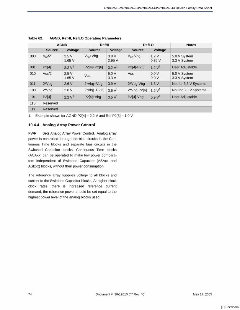
CY8C25122/CY8C26233/CY8C26443/CY8C26643 Device Family Data Sheet
10.4.4 Analog Array Power Control
PWR Sets Analog Array Power Control. Analog array
power is controlled through the bias circuits in the Con-
tinuous Time blocks and separate bias circuits in the
Switched Capacitor blocks. Continuous Time blocks
(ACAxx) can be operated to make low power compara-
tors independent of Switched Capacitor (ASAxx and
ASBxx) blocks, without their power consumption.
The reference array supplies voltage to all blocks and
current to the Switched Capacitor blocks. At higher block
clock rates, there is increased reference current
demand; the reference power should be set equal to the
highest power level of the analog blocks used.
Table 62: AGND, RefHI, RefLO Operating Parameters
AGND RefHI RefLO NotesSource Voltage Source Voltage Source Voltage
000 Vcc/2 2.5 V1.65 V
Vcc+Vbg 3.8 V2.95 V
Vcc-Vbg 1.2 V0.35 V
5.0 V System3.3 V System
001 P2[4] 2.2 V1 P2[4]+P2[6] 3.2 V1 P2[4]-P2[6] 1.2 V1 User Adjustable
010 Vcc/2 2.5 V1.65 V
Vcc5.0 V3.3 V
Vss 0.0 V0.0 V
5.0 V System3.3 V System
011 2*Vbg 2.6 V 2*Vbg+Vbg 3.9 V 2*Vbg-Vbg 1.3 V Not for 3.3 V Systems
100 2*Vbg 2.6 V 2*Vbg+P2[6] 3.6 V1 2*Vbg-P2[6] 1.6 V1 Not for 3.3 V Systems
101 P2[4] 2.2 V1 P2[4]+Vbg 3.5 V1 P2[4]-Vbg 0.9 V1 User Adjustable
110 Reserved
111 Reserved
1. Example shown for AGND P2[4] = 2.2 V and Ref P2[6] = 1.0 V
74 Document #: 38-12010 CY Rev. *C May 17, 2005
[+] Feedback
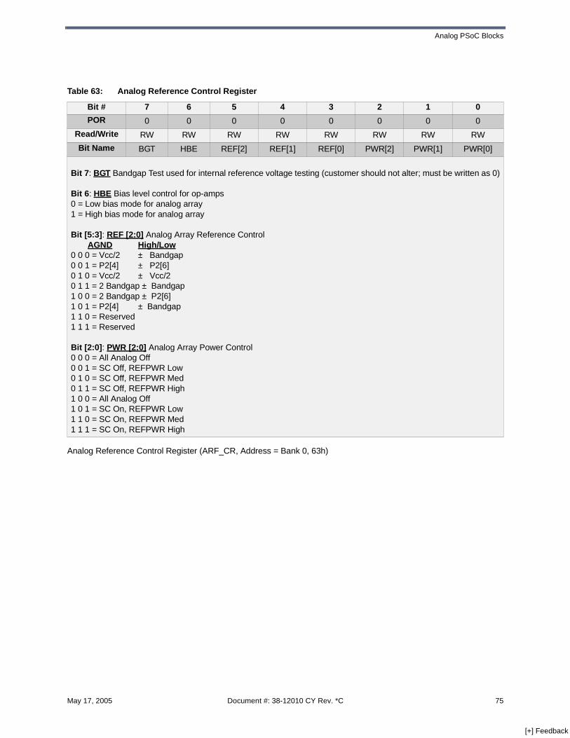
Analog PSoC Blocks
Analog Reference Control Register (ARF_CR, Address = Bank 0, 63h)
Table 63: Analog Reference Control Register
Bit # 7 6 5 4 3 2 1 0
POR 0 0 0 0 0 0 0 0
Read/Write RW RW RW RW RW RW RW RW
Bit Name BGT HBE REF[2] REF[1] REF[0] PWR[2] PWR[1] PWR[0]
Bit 7: BGT Bandgap Test used for internal reference voltage testing (customer should not alter; must be written as 0)
Bit 6: HBE Bias level control for op-amps0 = Low bias mode for analog array1 = High bias mode for analog array
Bit [5:3]: REF [2:0] Analog Array Reference ControlAGND High/Low
0 0 0 = Vcc/2 ± Bandgap 0 0 1 = P2[4] ± P2[6]0 1 0 = Vcc/2 ± Vcc/20 1 1 = 2 Bandgap ± Bandgap1 0 0 = 2 Bandgap ± P2[6]1 0 1 = P2[4] ± Bandgap1 1 0 = Reserved1 1 1 = Reserved
Bit [2:0]: PWR [2:0] Analog Array Power Control0 0 0 = All Analog Off0 0 1 = SC Off, REFPWR Low0 1 0 = SC Off, REFPWR Med0 1 1 = SC Off, REFPWR High1 0 0 = All Analog Off1 0 1 = SC On, REFPWR Low1 1 0 = SC On, REFPWR Med1 1 1 = SC On, REFPWR High
May 17, 2005 Document #: 38-12010 CY Rev. *C 75
[+] Feedback

CY8C25122/CY8C26233/CY8C26443/CY8C26643 Device Family Data Sheet
10.5 Analog PSoC Block Clocking Options
All analog PSoC blocks in a particular Analog Column
share the same clock signal. Choosing the clocking for
an analog PSoC block is a two-step process.
1. First, if the user wants to use the ACLK0 and ACLK1 system-clocking signals, the digital PSoC blocks that serve as the source for these signals must be selected. This selection is made in the Ana-log Clock Select Register (CLK_CR1).
2. Next, the user must select the source for the Acolumn0, Acolumn1, Acolumn2, and Acolumn3 system-clocking signals. The user will choose the clock for Acolumnx[1:0] bits in the Analog Column Clock Select Register (CLK_CR0). Each analog PSoC block in a particular Analog Column is clocked from the Acolumn[x] system-clocking sig-nal for that column. (Note that the Acolumn[x] sig-nals have a 1:4 divider on them.)
10.5.1 Analog Column Clock Select Register
Analog Column Clock Select Register (CLK_CR0, Address = Bank 1, 60h)
Table 64: Analog Column Clock Select Register
Bit # 7 6 5 4 3 2 1 0
POR 0 0 0 0 0 0 0 0Read/Write RW RW RW RW RW RW RW RW
Bit Name Acolumn3 [1]
Acolumn3 [0]
Acolumn2 [1]
Acolumn2 [0]
Acolumn1 [1]
Acolumn1 [0]
Acolumn0 [1]
Acolumn0 [0]
Bit [7:6]: Acolumn3 [1:0]0 0 = 24V10 1 = 24V21 0 = ACLK01 1 = ACLK1
Bit [5:4]: Acolumn2 [1:0]0 0 = 24V10 1 = 24V21 0 = ACLK01 1 = ACLK1
Bit [3:2]: Acolumn1 [1:0]0 0 = 24V10 1 = 24V21 0 = ACLK01 1 = ACLK1
Bit [1:0]: Acolumn0 [1:0]0 0 = 24V10 1 = 24V21 0 = ACLK01 1 = ACLK1
76 Document #: 38-12010 CY Rev. *C May 17, 2005
[+] Feedback

Analog PSoC Blocks
10.6 Analog Clock Select Register
Analog Clock Select Register (CLK_CR1, Address = Bank 1, 61h)
There are a total of twelve analog PSoC blocks imple-
mented for each of the following types; Analog Continu-
ous Time Type A (ACAxx), Analog Switch Cap Type A
(ASAxx), and Analog Switch Cap Type B (ASBxx).
These blocks are arranged in an array of three rows by
four columns. Each column has one of each type of
PSoC block, and the individual PSoC blocks are identi-
fied by the row and column in which they reside.
There are two primary types of analog PSoC blocks.
Both types contain one op-amp but their principles of
operation are quite different. Continuous-time PSoC
blocks employ three configuration registers and use
resistors to condition amplifier response. Switched
capacitor blocks have one comparator and four configu-
ration registers and operate as discrete-time sampling
operators. In both types, the configuration registers are
Table 65: Analog Clock Select Register
Bit # 7 6 5 4 3 2 1 0
POR 0 0 0 0 0 0 0 0Read/Write RW RW RW RW RW RW RW RW
Bit Name Reserved SHDIS ACLK1 [2] ACLK1 [1] ACLK1 [0] ACLK0 [2] ACLK0 [1] ACLK0 [0]
Bit 7: Reserved
Bit 6: SHDIS During normal operation of an SC block for the amplifier of a column enabled to drive the output bus, the connection is only made for the last half of PHI2 (during PHI1 and for the first half of PHI2, the output bus floats at the last voltage to which it was driven). This forms a sample and hold operation using the output bus and its asso-ciated capacitance. This design prevents the output bus from being perturbed by the intermediate states of the SC operation (often a reset state for PHI1 and settling to the valid state during PHI2)
Following are the exceptions: 1) If the ClockPhase bit in CR0 (for the SC block in question) is set to 1, then the out-put is enabled for the whole of PHI2. 2) If the SHDIS signal is set in bit 6 of the Analog Clock Select Register, then sample and hold operation is disabled for all columns and all enabled outputs of SC blocks are connected to their respective output busses for the entire period of their respective PHI2s
0 = Sample and hold function enabled 1 = Sample and hold function disabled
Bit [5:3]: ACLK1 [2:0]0 0 0 = Digital Basic Type A Block 000 0 1 = Digital Basic Type A Block 010 1 0 = Digital Basic Type A Block 020 1 1 = Digital Basic Type A Block 031 0 0 = Digital Communications Type A Block 041 0 1 = Digital Communications Type A Block 051 1 0 = Digital Communications Type A Block 061 1 1 = Digital Communications Type A Block 07
Bit [2:0]: ACLK0 [2:0] Same configurations as ACLK1 [2:0]0 0 0 = Digital Basic Type A Block 000 0 1 = Digital Basic Type A Block 010 1 0 = Digital Basic Type A Block 020 1 1 = Digital Basic Type A Block 031 0 0 = Digital Communications Type A Block 041 0 1 = Digital Communications Type A Block 051 1 0 = Digital Communications Type A Block 061 1 1 = Digital Communications Type A Block 07
May 17, 2005 Document #: 38-12010 CY Rev. *C 77
[+] Feedback
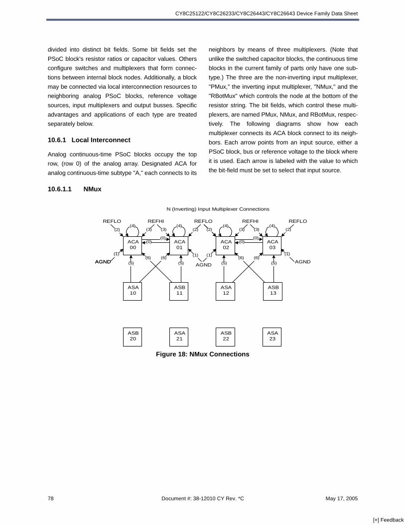
CY8C25122/CY8C26233/CY8C26443/CY8C26643 Device Family Data Sheet
divided into distinct bit fields. Some bit fields set the
PSoC block's resistor ratios or capacitor values. Others
configure switches and multiplexers that form connec-
tions between internal block nodes. Additionally, a block
may be connected via local interconnection resources to
neighboring analog PSoC blocks, reference voltage
sources, input multiplexers and output busses. Specific
advantages and applications of each type are treated
separately below.
10.6.1 Local Interconnect
Analog continuous-time PSoC blocks occupy the top
row, (row 0) of the analog array. Designated ACA for
analog continuous-time subtype "A," each connects to its
neighbors by means of three multiplexers. (Note that
unlike the switched capacitor blocks, the continuous time
blocks in the current family of parts only have one sub-
type.) The three are the non-inverting input multiplexer,
"PMux," the inverting input multiplexer, "NMux," and the
"RBotMux" which controls the node at the bottom of the
resistor string. The bit fields, which control these multi-
plexers, are named PMux, NMux, and RBotMux, respec-
tively. The following diagrams show how each
multiplexer connects its ACA block connect to its neigh-
bors. Each arrow points from an input source, either a
PSoC block, bus or reference voltage to the block where
it is used. Each arrow is labeled with the value to which
the bit-field must be set to select that input source.
10.6.1.1 NMux
Figure 18: NMux Connections
N (Inverting) Input Multiplexer Connections
ASB20
ACA00
ACA01
ACA02
ACA03
ASA10
ASB11
ASA12
ASB13
ASA21
ASB22
ASA23
(6)(5)
REFLO
AGND
(3)(6)
(5) AGND
(1)(1)
AGND
(1) (3)
AGND
(1)
(0)(0)
(0)(0)
(6)(5)
(6)(5)
(3) (2) (3) (2)
REFHI REFHIREFLO REFLO
(3) (3)(2)(2)(3)(4) (3)(4) (3)(4) (3)(4)
78 Document #: 38-12010 CY Rev. *C May 17, 2005
[+] Feedback

Analog PSoC Blocks
10.6.1.2 PMux
10.6.1.3 RBotMux
Figure 19: PMux Connections
P (Non-inverting) Input Multiplexer Connections
REFLO
ASB20
ACA00
ACA01
ACA02
ACA03
ASA10
ASB11
ASA12
ASB13
ASA21
ASB22
ASA23
(0)
(5)(4)
(1) (1) (1) (1)
(0) (0)REFLO (0)
AGND
(3)(5)
(4) AGND
(3)(3)
AGND
(3) (3)
AGND
(3)
(2)(2)
(2)(2)
(5)(4)
(5)(4)
(6)
ABUS 0
(6) (6) (6)
PortInputs
PortInputs
PortInputs
PortInputs
ABUS 1 ABUS 2 ABUS 3
Figure 20: RBotMux Connections
RB Input Multiplexer Connections
ASB20
ACA00
ACA01
ACA02
ACA03
ASA10
ASB11
ASA12
ASB13
ASA21
ASB22
ASA23
(3)
VSS
AGND
(3)
(3)AGND
(1)
AGND
(1)
AGND
(0)(0)
(0)(0)
(3) (3)
(2) (3)(2)(2)
VSS
VSS
VSS
(1) (3)(1)
May 17, 2005 Document #: 38-12010 CY Rev. *C 79
[+] Feedback

CY8C25122/CY8C26233/CY8C26443/CY8C26643 Device Family Data Sheet
10.7 Analog Continuous Time PSoC Blocks
10.7.1 Introduction
The Analog Continuous Time PSoC blocks are built
around an operational amplifier. There are several ana-
log muxes that are controlled by register-bit settings in
the control registers that determine the signal topology
inside the block. There is also a precision resistor matrix
that is located in the feedback path for the op-amp, and
is controlled by register-bit setting. There is also an ana-
log comparator connected to the output OUT, which con-
verts analog comparisons into digital signals.
There are five discrete outputs from this block. These
outputs are:
1. The analog output bus (ABUS), which is an analog bus resource that is shared by all of the analog blocks in the analog column for that block.
2. The comparator bus (CBUS), which is a digital bus that is a resource that is shared by all of the analog blocks in a column for that block.
3. The output bus (OUT, GOUT and LOUT), which is an analog bus resource that is shared by all of the analog blocks in a column and connects to one of the analog output buffers, to send a signal externally to the device.
This block supports Programmable Gain or attenuation
Op-Amp Circuits, (Differential Gain) Instrumentation
Amplifiers (using two CT Blocks), Continuous time high
frequency anti-aliasing filters, and modest response-time
analog comparators.
80 Document #: 38-12010 CY Rev. *C May 17, 2005
[+] Feedback

Analog PSoC Blocks
10.7.2 Registers
10.7.2.1 Analog Continuous Time Block xx Control 0 Register
The RTopMux and RBotMux bits control the connection
of the two ends of the resistor string. The RTopMux bit
controls the top end of the resistor string, which can
either be connected to Vcc or to the op-amp output. The
RBotMux bits control the connection of the bottom end of
the resistor string.
The RTapMux bits control the center tap of the resistor
string. Note that only relative weighting of units is given
in the table.
The Gain and Loss columns correspond to the gain or
loss obtained if the RTopMux and Gain bits are set so
that the overall amplifier provides gain or loss.
The Gain bit controls whether the resistor string is con-
nected around the op-amp as for gain (center tap to
Figure 21: Analog Continuous Time PSoC Blocks
RBotMux
Block Inputs
Block Inputs
PMux
AGND
AGND
ABUS
NMux
REFHI, LO
Power
CompCap
AGND VSS
SCBLK
RTapMux
GOUT
LOUT
Gain
RE
SIS
TO
RM
AT
RIX
Port Input
GIN
LIN
FB
ABUSAnalogBus
OUT
CBUSCompBus
CPhase
CLatch
Gain
TestMux
REFHI
AGND
PMuxOut
REFLO
VCC
RTopMux
May 17, 2005 Document #: 38-12010 CY Rev. *C 81
[+] Feedback
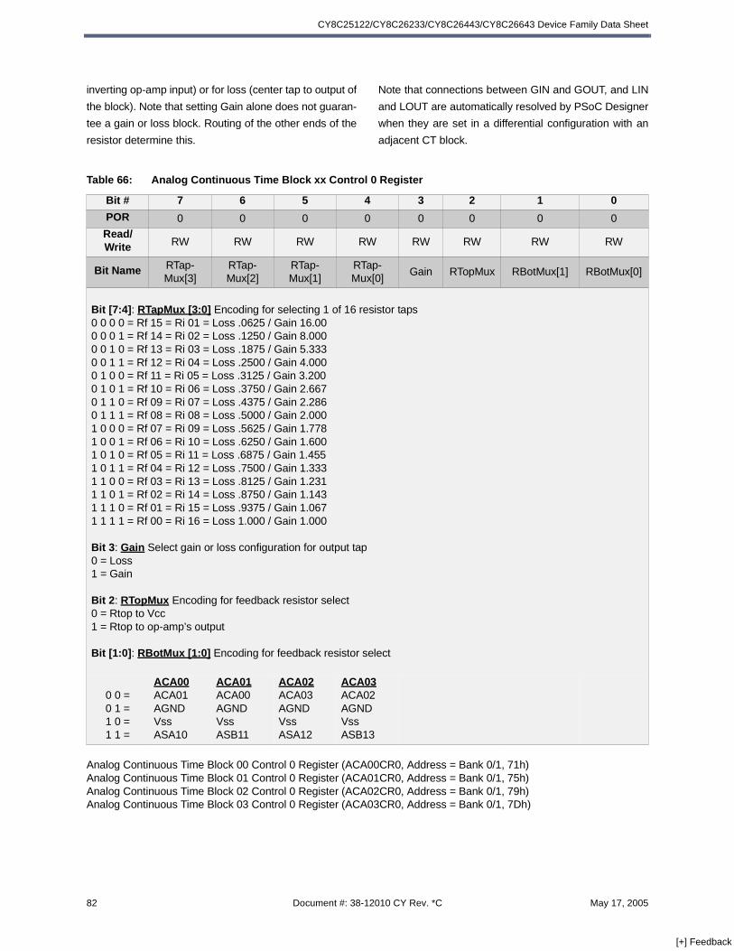
CY8C25122/CY8C26233/CY8C26443/CY8C26643 Device Family Data Sheet
inverting op-amp input) or for loss (center tap to output of
the block). Note that setting Gain alone does not guaran-
tee a gain or loss block. Routing of the other ends of the
resistor determine this.
Note that connections between GIN and GOUT, and LIN
and LOUT are automatically resolved by PSoC Designer
when they are set in a differential configuration with an
adjacent CT block.
Analog Continuous Time Block 00 Control 0 Register (ACA00CR0, Address = Bank 0/1, 71h)Analog Continuous Time Block 01 Control 0 Register (ACA01CR0, Address = Bank 0/1, 75h)Analog Continuous Time Block 02 Control 0 Register (ACA02CR0, Address = Bank 0/1, 79h)Analog Continuous Time Block 03 Control 0 Register (ACA03CR0, Address = Bank 0/1, 7Dh)
Table 66: Analog Continuous Time Block xx Control 0 Register
Bit # 7 6 5 4 3 2 1 0
POR 0 0 0 0 0 0 0 0Read/Write RW RW RW RW RW RW RW RW
Bit Name RTap-Mux[3]
RTap-Mux[2]
RTap-Mux[1]
RTap-Mux[0]
Gain RTopMux RBotMux[1] RBotMux[0]
Bit [7:4]: RTapMux [3:0] Encoding for selecting 1 of 16 resistor taps0 0 0 0 = Rf 15 = Ri 01 = Loss .0625 / Gain 16.000 0 0 1 = Rf 14 = Ri 02 = Loss .1250 / Gain 8.0000 0 1 0 = Rf 13 = Ri 03 = Loss .1875 / Gain 5.3330 0 1 1 = Rf 12 = Ri 04 = Loss .2500 / Gain 4.0000 1 0 0 = Rf 11 = Ri 05 = Loss .3125 / Gain 3.2000 1 0 1 = Rf 10 = Ri 06 = Loss .3750 / Gain 2.6670 1 1 0 = Rf 09 = Ri 07 = Loss .4375 / Gain 2.2860 1 1 1 = Rf 08 = Ri 08 = Loss .5000 / Gain 2.0001 0 0 0 = Rf 07 = Ri 09 = Loss .5625 / Gain 1.7781 0 0 1 = Rf 06 = Ri 10 = Loss .6250 / Gain 1.6001 0 1 0 = Rf 05 = Ri 11 = Loss .6875 / Gain 1.4551 0 1 1 = Rf 04 = Ri 12 = Loss .7500 / Gain 1.3331 1 0 0 = Rf 03 = Ri 13 = Loss .8125 / Gain 1.2311 1 0 1 = Rf 02 = Ri 14 = Loss .8750 / Gain 1.1431 1 1 0 = Rf 01 = Ri 15 = Loss .9375 / Gain 1.0671 1 1 1 = Rf 00 = Ri 16 = Loss 1.000 / Gain 1.000
Bit 3: Gain Select gain or loss configuration for output tap0 = Loss1 = Gain
Bit 2: RTopMux Encoding for feedback resistor select0 = Rtop to Vcc1 = Rtop to op-amp’s output
Bit [1:0]: RBotMux [1:0] Encoding for feedback resistor select
0 0 =0 1 =1 0 =1 1 =
ACA00ACA01AGNDVssASA10
ACA01ACA00AGNDVssASB11
ACA02ACA03AGNDVssASA12
ACA03ACA02AGNDVssASB13
82 Document #: 38-12010 CY Rev. *C May 17, 2005
[+] Feedback
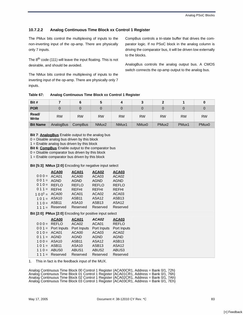
Analog PSoC Blocks
10.7.2.2 Analog Continuous Time Block xx Control 1 Register
The PMux bits control the multiplexing of inputs to the
non-inverting input of the op-amp. There are physically
only 7 inputs.
The 8th code (111) will leave the input floating. This is not
desirable, and should be avoided.
The NMux bits control the multiplexing of inputs to the
inverting input of the op-amp. There are physically only 7
inputs.
CompBus controls a tri-state buffer that drives the com-
parator logic. If no PSoC block in the analog column is
driving the comparator bus, it will be driven low externally
to the blocks.
AnalogBus controls the analog output bus. A CMOS
switch connects the op-amp output to the analog bus.
Analog Continuous Time Block 00 Control 1 Register (ACA00CR1, Address = Bank 0/1, 72h)Analog Continuous Time Block 01 Control 1 Register (ACA01CR1, Address = Bank 0/1, 76h)Analog Continuous Time Block 02 Control 1 Register (ACA02CR1, Address = Bank 0/1, 7Ah)Analog Continuous Time Block 03 Control 1 Register (ACA03CR1, Address = Bank 0/1, 7Eh)
Table 67: Analog Continuous Time Block xx Control 1 Register
Bit # 7 6 5 4 3 2 1 0
POR 0 0 0 0 0 0 0 0
Read/Write
RW RW RW RW RW RW RW RW
Bit Name AnalogBus CompBus NMux2 NMux1 NMux0 PMux2 PMux1 PMux0
Bit 7: AnalogBus Enable output to the analog bus 0 = Disable analog bus driven by this block1 = Enable analog bus driven by this blockBit 6: CompBus Enable output to the comparator bus0 = Disable comparator bus driven by this block1 = Enable comparator bus driven by this block
Bit [5:3]: NMux [2:0] Encoding for negative input select
0 0 0 =0 0 1 =0 1 0 =0 1 1 =
1 0 01 =1 0 1 =1 1 0 =1 1 1 =
ACA00ACA01AGNDREFLOREFHIACA00ASA10ASB11Reserved
ACA01ACA00AGNDREFLOREFHIACA01ASB11ASA10Reserved
ACA02ACA03AGNDREFLOREFHIACA02ASA12ASB13Reserved
ACA03ACA02AGNDREFLOREFHIACA03ASB13ASA12Reserved
Bit [2:0]: PMux [2:0] Encoding for positive input select
0 0 0 =0 0 1 =0 1 0 =0 1 1 =1 0 0 =1 0 1 =1 1 0 =1 1 1 =
ACA00REFLOPort InputsACA01AGNDASA10ASB11ABUS0Reserved
ACA01ACA02Port InputsACA00AGNDASB11ASA10ABUS1Reserved
ACA02ACA01Port InputsACA03AGNDASA12ASB13ABUS2Reserved
ACA03REFLOPort InputsACA02AGNDASB13ASA12ABUS3Reserved
1. This in fact is the feedback input of the MUX.
May 17, 2005 Document #: 38-12010 CY Rev. *C 83
[+] Feedback

CY8C25122/CY8C26233/CY8C26443/CY8C26643 Device Family Data Sheet
10.7.2.3 Analog Continuous Time Type A Block xx Control 2 Register
CPhase controls which internal clock phase the compar-
ator data is latched on.
CLatch controls whether the latch is active or if it is
always transparent.
CompCap controls whether the compensation capacitor
is switched in or not in the op-amp. By not switching in
the compensation capacitance, a much faster response
can be obtained if the amplifier is being used as a com-
parator.
TestMux – selects block bypass mode for testing and
characterization purposes.
Power – encoding for selecting 1 of 4 power levels. The
blocks always power up in the off state.
Analog Continuous Time Block 00 Control 2 Register (ACA00CR2, Address = Bank 0/1, 73h)Analog Continuous Time Block 01 Control 2 Register (ACA01CR2, Address = Bank 0/1, 77h)Analog Continuous Time Block 02 Control 2 Register (ACA02CR2, Address = Bank 0/1, 7Bh)Analog Continuous Time Block 03 Control 2 Register (ACA03CR2, Address = Bank 0/1, 7Fh)
Table 68: Analog Continuous Time Type A Block xx Control 2 Register
Bit # 7 6 5 4 3 2 1 0
POR 0 0 0 0 0 0 0 0Read/Write RW RW RW RW RW RW RW RW
Bit Name CPhase CLatch CompCap TestMux[2] TestMux[1] TestMux[0] Power[1] Power[0]
Bit 7: CPhase0 = Comparator Control latch transparent on PHI11 = Comparator Control latch transparent on PHI2
Bit 6: CLatch0 = Comparator Control latch is always transparent1 = Comparator Control latch is active
Bit 5: CompCap0 = Comparator Mode 1 = Op-amp Mode
Bit [4:2]: TestMux [2:0] Select block bypass mode for testing and characterization purposes ACA00 ACA01 ACA02 ACA031 0 0 = Positive Input to…ABUS0 ABUS1 ABUS2 ABUS31 0 1 = AGND to… ABUS0 ABUS1 ABUS2 ABUS31 1 0 = REFLO to… ABUS0 ABUS1 ABUS2 ABUS31 1 1 = REFHI to… ABUS0 ABUS1 ABUS2 ABUS30 x x = All Paths Off
Bit [1:0]: Power [1:0] Encoding for selecting 1 of 4 power levels0 0 = Off0 1 = Low (60 µA)1 0 = Med (150 µA)1 1 = High (500 µA)
84 Document #: 38-12010 CY Rev. *C May 17, 2005
[+] Feedback

Analog PSoC Blocks
10.8 Analog Switch Cap Type A PSoC Blocks
10.8.1 Introduction
The Analog Switch Cap Type A PSoC blocks are built
around an operational amplifier. There are several ana-
log muxes that are controlled by register-bit settings in
the control registers that determine the signal topology
inside the block. There are also four arrays of unit value
capacitors that are located in the feedback path for the
op-amp, and are switched by two phase clocks, PHI1
and PHI2. These four capacitor arrays are labeled A Cap
Array, B Cap Array, C Cap Array, and F Cap Array. There
is also an analog comparator connected to the output
OUT, which converts analog comparisons into digital sig-
nals.
There are three discrete outputs from this block. These
outputs are:
1. The analog output bus (ABUS), which is an analog bus resource that is shared by all of the analog blocks in the analog column for that block.
2. The comparator bus (CBUS), which is a digital bus that is a resource that is shared by all of the analog blocks in a column for that block.
3. The output bus (OUT), which is an analog bus resource that is shared by all of the analog blocks in a column and connects to one of the analog output buffers, to send a signal externally to the device.
SC Integrator Block A supports Delta-Sigma, Successive
Approximation and Incremental A/D Conversion, Capaci-
tor DACs, and SC filters. It has three input arrays of bina-
rily-weighted switched capacitors, allowing user
programmability of the capacitor weights. This provides
summing capability of two (CDAC) scaled inputs, and a
non-switched capacitor input. Since the input of SC
Block A has this additional switched capacitor, it is con-
figured for the input stage of such a switched capacitor
biquad filter. When followed by an SC Block B Integrator,
this combination of blocks can be used to provide a full
Switched Capacitor Biquad.
May 17, 2005 Document #: 38-12010 CY Rev. *C 85
[+] Feedback
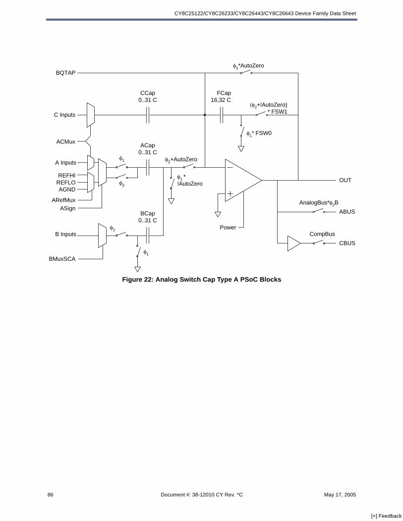
CY8C25122/CY8C26233/CY8C26443/CY8C26643 Device Family Data Sheet
Figure 22: Analog Switch Cap Type A PSoC Blocks
φ1* FSW0
φ1 *!AutoZero
BMuxSCA
BQTAP
ABUS
CBUS
C Inputs
CCap0..31 C
BCap0..31 C
ACap0..31 C
FCap16,32 C
φ2
φ2+AutoZero
φ1*AutoZero
(φ2+!AutoZero)* FSW1
Power
AnalogBus*φ2B
CompBus
φ1
ASignARefMux
OUTφ2
φ1
REFHIREFLOAGND
ACMux
A Inputs
B Inputs
86 Document #: 38-12010 CY Rev. *C May 17, 2005
[+] Feedback
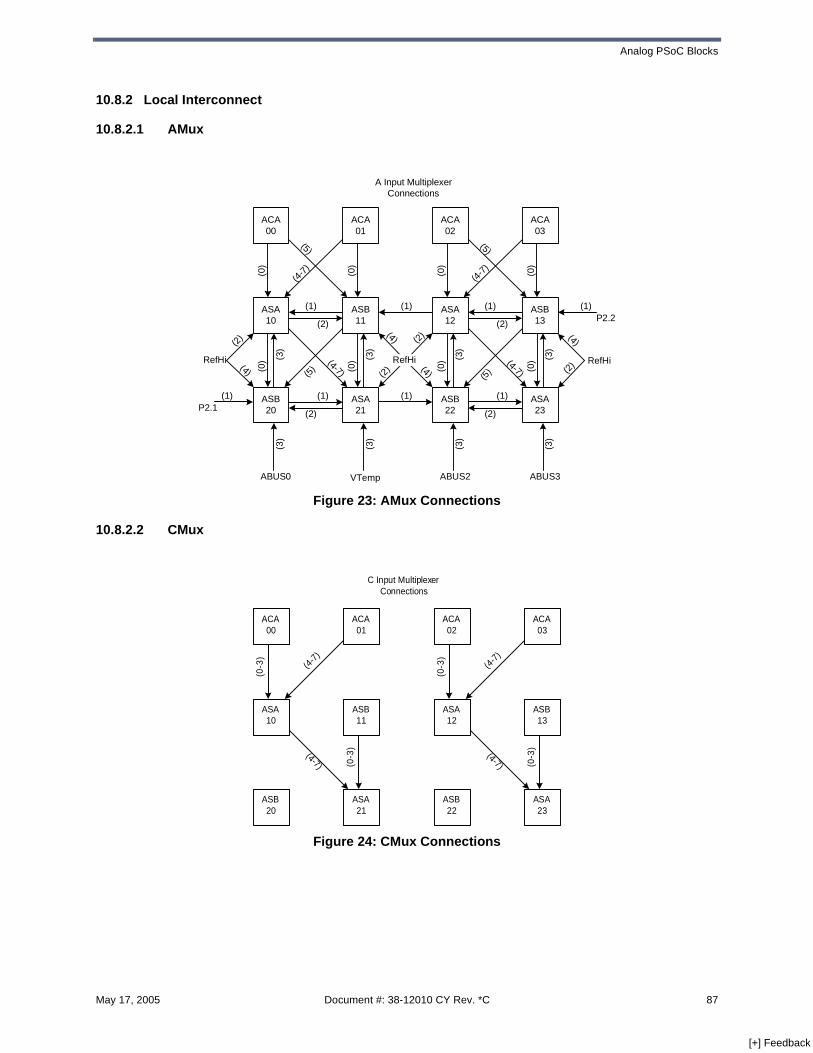
Analog PSoC Blocks
10.8.2 Local Interconnect
10.8.2.1 AMux
10.8.2.2 CMux
Figure 23: AMux Connections
A Input MultiplexerConnections
(1)
(2)
(1) (1)
(2)
(1)
(2)
(1)(1)
(2)
(3)
(4-7
)(0
)
(5)
(4) (2)
(0)
(0)
(0)
(0)
(0)
(0)
(0)(3
)
(3)
(3)
(4-7)
(5)
(4-7
)
(5)
(4-7)
(5)
RefHi
(2) (4)
(2)
RefHi(4)
(4)
RefHi(2
)
P2.2
P2.1
ABUS0 ABUS2 ABUS3VTemp
(3)
(3)
(3)
(3)
(1)
(1) ASB20
ACA00
ACA01
ACA02
ACA03
ASA10
ASB11
ASA12
ASB13
ASA21
ASB22
ASA23
Figure 24: CMux Connections
C Input MultiplexerConnections
ASB20
ACA00
ACA01
ACA02
ACA03
ASA10
ASB11
ASA12
ASB13
ASA21
ASB22
ASA23
(0-3
)
(4-7) (0-3
)
(4-7
)
(0-3
)
(4-7) (0-3
)
(4-7
)
May 17, 2005 Document #: 38-12010 CY Rev. *C 87
[+] Feedback
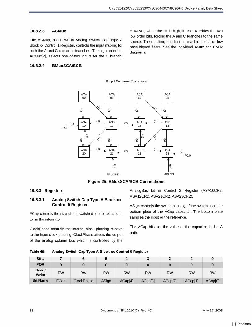
CY8C25122/CY8C26233/CY8C26443/CY8C26643 Device Family Data Sheet
10.8.2.3 ACMux
The ACMux, as shown in Analog Switch Cap Type ABlock xx Control 1 Register, controls the input muxing forboth the A and C capacitor branches. The high order bit,ACMux[2], selects one of two inputs for the C branch.
However, when the bit is high, it also overrides the twolow order bits, forcing the A and C branches to the samesource. The resulting condition is used to construct lowpass biquad filters. See the individual AMux and CMuxdiagrams.
10.8.2.4 BMuxSCA/SCB
10.8.3 Registers
10.8.3.1 Analog Switch Cap Type A Block xx Control 0 Register
FCap controls the size of the switched feedback capaci-
tor in the integrator.
ClockPhase controls the internal clock phasing relative
to the input clock phasing. ClockPhase affects the output
of the analog column bus which is controlled by the
AnalogBus bit in Control 2 Register (ASA10CR2,
ASA12CR2, ASA21CR2, ASA23CR2).
ASign controls the switch phasing of the switches on the
bottom plate of the ACap capacitor. The bottom plate
samples the input or the reference.
The ACap bits set the value of the capacitor in the A
path.
Figure 25: BMuxSCA/SCB Connections
B Input Multiplexer Connections
ASB20
ACA00
ACA01
ACA02
ACA03
ASA10
ASB11
ASA12
ASB13
ASA21
ASB22
ASA23
(1)(2)
(1)
(1)(2)
(1)
(3)
(0)
(1)
(0)
(0)
(0)
(0)
(0)
(0)
(0)(3
)
(1)
(1)
(1)
P2.0
P2.3
ABUS3TRefGND
(3)
(3)
(2)
(2)
Table 69: Analog Switch Cap Type A Block xx Control 0 Register
Bit # 7 6 5 4 3 2 1 0
POR 0 0 0 0 0 0 0 0Read/Write RW RW RW RW RW RW RW RW
Bit Name FCap ClockPhase ASign ACap[4] ACap[3] ACap[2] ACap[1] ACap[0]
88 Document #: 38-12010 CY Rev. *C May 17, 2005
[+] Feedback

Analog PSoC Blocks
Analog Switch Cap Type A Block 10 Control 0 Register (ASA10CR0, Address = Bank 0/1, 80h)Analog Switch Cap Type A Block 12 Control 0 Register (ASA12CR0, Address = Bank 0/1, 88h)Analog Switch Cap Type A Block 21 Control 0 Register (ASA21CR0, Address = Bank 0/1, 94h)Analog Switch Cap Type A Block 23 Control 0 Register (ASA23CR0, Address = Bank 0/1, 9Ch)
Bit 7: FCap F Capacitor value selection bit0 = 16 capacitor units1 = 32 capacitor units
Bit 6: ClockPhase Clock phase select, will invert clocks internal to the blocks. During normal operation of an SC block for the amplifier of a column enabled to drive the output bus, the connection is only made for the last half of PHI2 (during PHI1 and for the first half of PHI2, the output bus floats at the last voltage to which it was driven). This forms a sample and hold operation using the output bus and its associated capacitance. This design prevents the output bus from being perturbed by the intermediate states of the SC operation (often a reset state for PHI1 and set-tling to the valid state during PHI2)
Following are the exceptions: 1) If the ClockPhase bit in CR0 (for the SC block in question) is set to 1, then the out-put is enabled for the whole of PHI2. 2) If the SHDIS signal is set in bit 6 of the Analog Clock Select Register, then sample and hold operation is disabled for all columns and all enabled outputs of SC blocks are connected to their respective output busses for the entire period of their respective PHI2s
0 = Internal PHI1 = External PHI11 = Internal PHI1 = External PHI2
This bit also affects the latching of the comparator output (CBUS). Both clock phases, PHI1 and PHI2, are involved in the output latching mechanism. The capture of the next value to be output from the latch (capture point event) hap-pens during the falling edge of one clock phase, and the rising edge of the other clock phase will cause the value to come out (output point event). This bit determines which clock phase triggers the capture point event, and the other clock will trigger the output point event. The value output to the comparator bus will remain stable between output point events.
0 = Capture Point Event triggered by Falling PHI2, Output Point Event triggered by Rising PHI11 = Capture Point Event triggered by Falling PHI1, Output Point Event triggered by Rising PHI2
Bit 5: ASign0 = Input sampled on Internal PHI1, Reference Input sampled on internal PHI21 = Input sampled on Internal PHI2, Reference Input sampled on internal PHI1
Bit [4:0]: ACap [4:0] Binary encoding for 32 possible capacitor sizes for A Capacitor:
0 0 0 0 0 = 0 Capacitor units in array0 0 0 0 1 = 1 Capacitor units in array0 0 0 1 0 = 2 Capacitor units in array0 0 0 1 1 = 3 Capacitor units in array0 0 1 0 0 = 4 Capacitor units in array0 0 1 0 1 = 5 Capacitor units in array0 0 1 1 0 = 6 Capacitor units in array0 0 1 1 1 = 7 Capacitor units in array0 1 0 0 0 = 8 Capacitor units in array0 1 0 0 1 = 9 Capacitor units in array0 1 0 1 0 = 10 Capacitor units in array0 1 0 1 1 = 11 Capacitor units in array0 1 1 0 0 = 12 Capacitor units in array0 1 1 0 1 = 13 Capacitor units in array0 1 1 1 0 = 14 Capacitor units in array0 1 1 1 1 = 15 Capacitor units in array
1 0 0 0 0 = 16 Capacitor units in array1 0 0 0 1 = 17 Capacitor units in array1 0 0 1 0 = 18 Capacitor units in array1 0 0 1 1 = 19 Capacitor units in array1 0 1 0 0 = 20 Capacitor units in array1 0 1 0 1 = 21 Capacitor units in array1 0 1 1 0 = 22 Capacitor units in array1 0 1 1 1 = 23 Capacitor units in array1 1 0 0 0 = 24 Capacitor units in array1 1 0 0 1 = 25 Capacitor units in array1 1 0 1 0 = 26 Capacitor units in array1 1 0 1 1 = 27 Capacitor units in array1 1 1 0 0 = 28 Capacitor units in array1 1 1 0 1 = 29 Capacitor units in array1 1 1 1 0 = 30 Capacitor units in array1 1 1 1 1 = 31 Capacitor units in array
Table 69: Analog Switch Cap Type A Block xx Control 0 Register, continued
May 17, 2005 Document #: 38-12010 CY Rev. *C 89
[+] Feedback
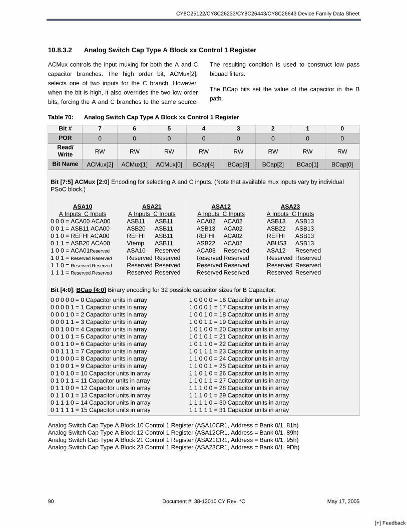
CY8C25122/CY8C26233/CY8C26443/CY8C26643 Device Family Data Sheet
10.8.3.2 Analog Switch Cap Type A Block xx Control 1 Register
ACMux controls the input muxing for both the A and C
capacitor branches. The high order bit, ACMux[2],
selects one of two inputs for the C branch. However,
when the bit is high, it also overrides the two low order
bits, forcing the A and C branches to the same source.
The resulting condition is used to construct low pass
biquad filters.
The BCap bits set the value of the capacitor in the B
path.
Analog Switch Cap Type A Block 10 Control 1 Register (ASA10CR1, Address = Bank 0/1, 81h)Analog Switch Cap Type A Block 12 Control 1 Register (ASA12CR1, Address = Bank 0/1, 89h)Analog Switch Cap Type A Block 21 Control 1 Register (ASA21CR1, Address = Bank 0/1, 95h)Analog Switch Cap Type A Block 23 Control 1 Register (ASA23CR1, Address = Bank 0/1, 9Dh)
Table 70: Analog Switch Cap Type A Block xx Control 1 Register
Bit # 7 6 5 4 3 2 1 0
POR 0 0 0 0 0 0 0 0Read/Write RW RW RW RW RW RW RW RW
Bit Name ACMux[2] ACMux[1] ACMux[0] BCap[4] BCap[3] BCap[2] BCap[1] BCap[0]
Bit [7:5] ACMux [2:0] Encoding for selecting A and C inputs. (Note that available mux inputs vary by individual PSoC block.)
ASA10A Inputs C Inputs
0 0 0 = ACA00 ACA000 0 1 = ASB11 ACA000 1 0 = REFHI ACA000 1 1 = ASB20 ACA001 0 0 = ACA01Reserved
1 0 1 = Reserved Reserved
1 1 0 = Reserved Reserved
1 1 1 = Reserved Reserved
ASA21A Inputs C InputsASB11 ASB11ASB20 ASB11REFHI ASB11Vtemp ASB11ASA10 ReservedReserved ReservedReserved ReservedReserved Reserved
ASA12A Inputs C InputsACA02 ACA02ASB13 ACA02REFHI ACA02ASB22 ACA02ACA03 ReservedReserved ReservedReserved ReservedReserved Reserved
ASA23A Inputs C InputsASB13 ASB13ASB22 ASB13REFHI ASB13ABUS3 ASB13ASA12 ReservedReserved ReservedReserved ReservedReserved Reserved
Bit [4:0]: BCap [4:0] Binary encoding for 32 possible capacitor sizes for B Capacitor:
0 0 0 0 0 = 0 Capacitor units in array0 0 0 0 1 = 1 Capacitor units in array0 0 0 1 0 = 2 Capacitor units in array0 0 0 1 1 = 3 Capacitor units in array0 0 1 0 0 = 4 Capacitor units in array0 0 1 0 1 = 5 Capacitor units in array0 0 1 1 0 = 6 Capacitor units in array0 0 1 1 1 = 7 Capacitor units in array0 1 0 0 0 = 8 Capacitor units in array0 1 0 0 1 = 9 Capacitor units in array0 1 0 1 0 = 10 Capacitor units in array0 1 0 1 1 = 11 Capacitor units in array0 1 1 0 0 = 12 Capacitor units in array0 1 1 0 1 = 13 Capacitor units in array0 1 1 1 0 = 14 Capacitor units in array0 1 1 1 1 = 15 Capacitor units in array
1 0 0 0 0 = 16 Capacitor units in array1 0 0 0 1 = 17 Capacitor units in array1 0 0 1 0 = 18 Capacitor units in array1 0 0 1 1 = 19 Capacitor units in array1 0 1 0 0 = 20 Capacitor units in array1 0 1 0 1 = 21 Capacitor units in array1 0 1 1 0 = 22 Capacitor units in array1 0 1 1 1 = 23 Capacitor units in array1 1 0 0 0 = 24 Capacitor units in array1 1 0 0 1 = 25 Capacitor units in array1 1 0 1 0 = 26 Capacitor units in array1 1 0 1 1 = 27 Capacitor units in array1 1 1 0 0 = 28 Capacitor units in array1 1 1 0 1 = 29 Capacitor units in array1 1 1 1 0 = 30 Capacitor units in array1 1 1 1 1 = 31 Capacitor units in array
90 Document #: 38-12010 CY Rev. *C May 17, 2005
[+] Feedback
Analog PSoC Blocks
10.8.3.3 Analog Switch Cap Type A Block xx Control 2 Register
AnalogBus gates the output to the analog column bus.
The output on the analog column bus is affected by the
state of the ClockPhase bit in Control 0 Register
(ASA10CR0, ASA12CR0, ASA21CR0, ASA23CR0). If
AnalogBus is set to 0, the output to the analog column
bus is tri-stated. If AnalogBus is set to 1, the signal that is
output to the analog column bus is selected by the
ClockPhase bit. If the ClockPhase bit is 0, the block out-
put is gated by sampling clock on last part of PHI2. If the
ClockPhase bit is 1, the block output continuously drives
the analog column bus.
CompBus controls the output to the column comparator
bus. Note that if the comparator bus is not driven by any-
thing in the column, it is pulled low. The comparator out-
put is evaluated on the rising edge of internal PHI1 and
is latched so it is available during internal PHI2.
AutoZero controls the shorting of the output to the invert-
ing input of the op-amp. When shorted, the op-amp is
basically a follower. The output is the op-amp offset. By
using the feedback capacitor of the integrator, the block
can memorize the offset and create an offset cancella-
tion scheme. AutoZero also controls a pair of switches
between the A and B branches and the summing node of
the op-amp. If AutoZero is enabled, then the pair of
switches is active. AutoZero also affects the function of
the FSW1 bit in Control 3 Register.
The CCap bits set the value of the capacitor in the C
path.
May 17, 2005 Document #: 38-12010 CY Rev. *C 91
[+] Feedback
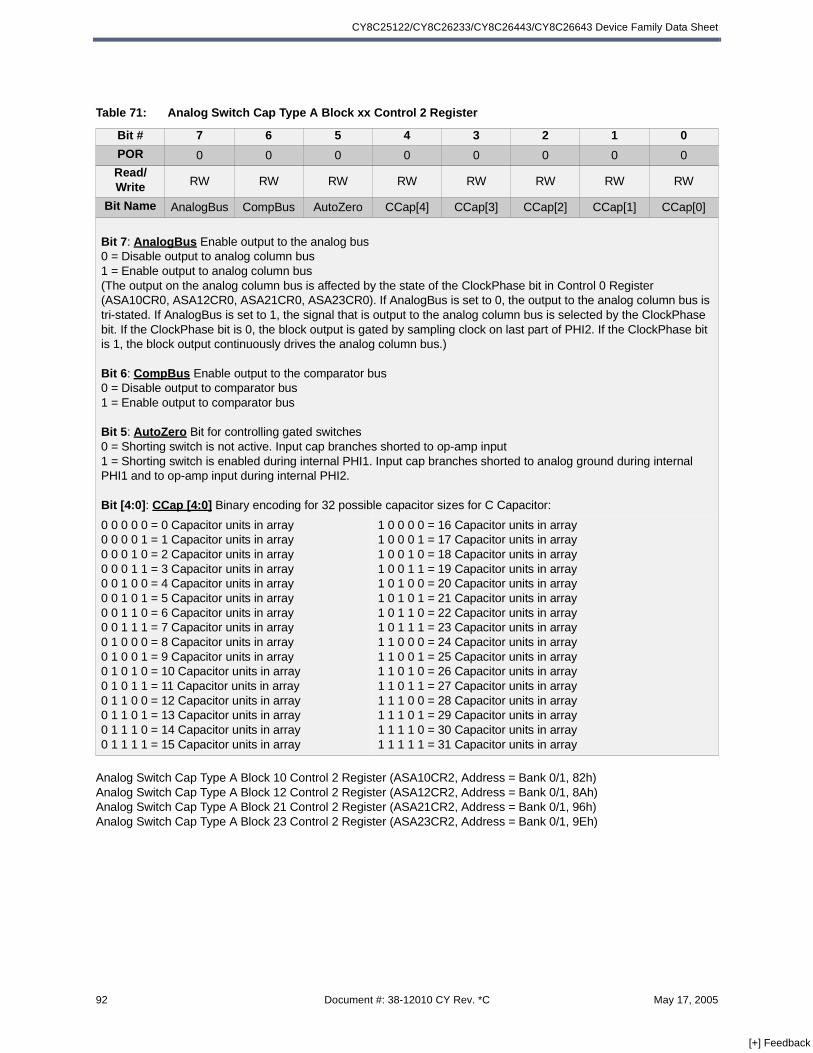
CY8C25122/CY8C26233/CY8C26443/CY8C26643 Device Family Data Sheet
Analog Switch Cap Type A Block 10 Control 2 Register (ASA10CR2, Address = Bank 0/1, 82h)Analog Switch Cap Type A Block 12 Control 2 Register (ASA12CR2, Address = Bank 0/1, 8Ah)Analog Switch Cap Type A Block 21 Control 2 Register (ASA21CR2, Address = Bank 0/1, 96h)Analog Switch Cap Type A Block 23 Control 2 Register (ASA23CR2, Address = Bank 0/1, 9Eh)
Table 71: Analog Switch Cap Type A Block xx Control 2 Register
Bit # 7 6 5 4 3 2 1 0
POR 0 0 0 0 0 0 0 0Read/Write RW RW RW RW RW RW RW RW
Bit Name AnalogBus CompBus AutoZero CCap[4] CCap[3] CCap[2] CCap[1] CCap[0]
Bit 7: AnalogBus Enable output to the analog bus0 = Disable output to analog column bus1 = Enable output to analog column bus (The output on the analog column bus is affected by the state of the ClockPhase bit in Control 0 Register (ASA10CR0, ASA12CR0, ASA21CR0, ASA23CR0). If AnalogBus is set to 0, the output to the analog column bus is tri-stated. If AnalogBus is set to 1, the signal that is output to the analog column bus is selected by the ClockPhase bit. If the ClockPhase bit is 0, the block output is gated by sampling clock on last part of PHI2. If the ClockPhase bit is 1, the block output continuously drives the analog column bus.)
Bit 6: CompBus Enable output to the comparator bus0 = Disable output to comparator bus1 = Enable output to comparator bus
Bit 5: AutoZero Bit for controlling gated switches0 = Shorting switch is not active. Input cap branches shorted to op-amp input1 = Shorting switch is enabled during internal PHI1. Input cap branches shorted to analog ground during internal PHI1 and to op-amp input during internal PHI2.
Bit [4:0]: CCap [4:0] Binary encoding for 32 possible capacitor sizes for C Capacitor:
0 0 0 0 0 = 0 Capacitor units in array0 0 0 0 1 = 1 Capacitor units in array0 0 0 1 0 = 2 Capacitor units in array0 0 0 1 1 = 3 Capacitor units in array0 0 1 0 0 = 4 Capacitor units in array0 0 1 0 1 = 5 Capacitor units in array0 0 1 1 0 = 6 Capacitor units in array0 0 1 1 1 = 7 Capacitor units in array0 1 0 0 0 = 8 Capacitor units in array0 1 0 0 1 = 9 Capacitor units in array0 1 0 1 0 = 10 Capacitor units in array0 1 0 1 1 = 11 Capacitor units in array0 1 1 0 0 = 12 Capacitor units in array0 1 1 0 1 = 13 Capacitor units in array0 1 1 1 0 = 14 Capacitor units in array0 1 1 1 1 = 15 Capacitor units in array
1 0 0 0 0 = 16 Capacitor units in array1 0 0 0 1 = 17 Capacitor units in array1 0 0 1 0 = 18 Capacitor units in array1 0 0 1 1 = 19 Capacitor units in array1 0 1 0 0 = 20 Capacitor units in array1 0 1 0 1 = 21 Capacitor units in array1 0 1 1 0 = 22 Capacitor units in array1 0 1 1 1 = 23 Capacitor units in array1 1 0 0 0 = 24 Capacitor units in array1 1 0 0 1 = 25 Capacitor units in array1 1 0 1 0 = 26 Capacitor units in array1 1 0 1 1 = 27 Capacitor units in array1 1 1 0 0 = 28 Capacitor units in array1 1 1 0 1 = 29 Capacitor units in array1 1 1 1 0 = 30 Capacitor units in array1 1 1 1 1 = 31 Capacitor units in array
92 Document #: 38-12010 CY Rev. *C May 17, 2005
[+] Feedback

Analog PSoC Blocks
10.8.3.4 Analog Switch Cap Type A Block xx Control 3 Register
ARefMux selects the reference input of the A capacitorbranch.
FSW1 is used to control a switch in the integrator capac-itor path. It connects the output of the op-amp to the inte-grating cap. The state of the switch is affected by thestate of the AutoZero bit in Control 2 Register(ASA10CR2, ASA12CR2, ASA21CR2, ASA23CR2). Ifthe FSW1 bit is set to 0, the switch is always disabled. Ifthe FSW1 bit is set to 1, the AutoZero bit determines thestate of the switch. If the AutoZero bit is 0, the switch is
enabled at all times. If the AutoZero bit is 1, the switch isenabled only when the internal PHI2 is high.
FSW0 is used to control a switch in the integrator capac-itor path. It connects the output of the op-amp to analogground.
BMuxSCA controls the muxing to the input of the Bcapacitor branch.
Power – encoding for selecting 1 of 4 power levels. Theblock always powers up in the off state.
Table 72: Analog Switch Cap Type A Block xx Control 3 Register
Analog Switch Cap Type A Block 10 Control 3 Register (ASA10CR3, Address = Bank 0/1, 83h)Analog Switch Cap Type A Block 12 Control 3 Register (ASA12CR3, Address = Bank 0/1, 8Bh)Analog Switch Cap Type A Block 21 Control 3 Register (ASA21CR3, Address = Bank 0/1, 97h)Analog Switch Cap Type A Block 23 Control 3 Register (ASA23CR3, Address = Bank 0/1, 9Fh)
Bit # 7 6 5 4 3 2 1 0
POR 0 0 0 0 0 0 0 0Read/Write RW RW RW RW RW RW RW RW
Bit Name ARefMux[1] ARefMux[0] FSW[1] FSW[0] BMuxSCA[1] BMuxSCA[0] Power[1] Power[0]
Bit [7:6]: ARefMux [1:0] Encoding for selecting reference input0 0 = Analog ground is selected0 1 = REFHI input selected (This is usually the high reference)1 0 = REFLO input selected (This is usually the low reference)1 1 = Reference selection is driven by the comparator (When output comparator node is set high, the input is set to REFHI. When set low, the input is set to REFLO)
Bit 5: FSW1 Bit for controlling gated switches0 = Switch is disabled1 = If the FSW1 bit is set to 1, the state of the switch is determined by the AutoZero bit. If the AutoZero bit is 0, the switch is enabled at all times. If the AutoZero bit is 1, the switch is enabled only when the internal PHI2 is high
Bit 4: FSW0 Bits for controlling gated switches0 = Switch is disabled1 = Switch is enabled when PHI1 is high
Bit [3:2] BMuxSCA [1:0] Encoding for selecting B inputs. (Note that the available mux inputs vary by individual PSoC block.) ASA10 ASA21 ASA12 ASA230 0 = ACA00 ASB11 ACA02 ASB130 1 = ASB11 ASB20 ASB13 ASB221 0 = P2.3 ASB22 ASB11 P2.01 1 = ASB20 TrefGND ASB22 ABUS3
Bit [1:0]: Power [1:0] Encoding for selecting 1 of 4 power levels0 0 = Off0 1 = 10 µA, typical1 0 = 50 µA, typical1 1 = 200 µA, typical
May 17, 2005 Document #: 38-12010 CY Rev. *C 93
[+] Feedback

CY8C25122/CY8C26233/CY8C26443/CY8C26643 Device Family Data Sheet
10.9 Analog Switch Cap Type B PSoC Blocks
10.9.1 Introduction
The Analog Switch Cap Type B PSoC blocks are built
around an operational amplifier. There are several ana-
log muxes that are controlled by register-bit settings in
the control registers that determine the signal topology
inside the block. There are also four arrays of unit value
capacitors that are located in the feedback path for the
op-amp, and are switched by two phase clocks, PHI1
and PHI2. These four capacitor arrays are labeled A Cap
Array, B Cap Array, C Cap Array, and F Cap Array. There
is also an analog comparator connected to the output
OUT, which converts analog comparisons into digital sig-
nals.
There are three discrete outputs from this block. These
outputs are:
1. The analog output bus (ABUS), which is an analog bus resource that is shared by all of the analog blocks in the analog column for that block.
2. The comparator bus (CBUS), which is a digital bus that is a resource that is shared by all of the analog blocks in a column for that block.
3. The output bus (OUT), which is an analog bus resource that is shared by all of the analog blocks in a column and connects to one of the analog output buffers, to send a signal externally to the device.
The SCB block also supports Delta-Sigma, Successive
Approximation and Incremental A/D Conversion, Capaci-
tor DACs, and SC filters. It has two input arrays of
switched capacitors, and a Non-Switched capacitor feed-
back array from the output. When preceded by an SC
Block A Integrator, the combination can be used to pro-
vide a full Switched Capacitor Biquad.
94 Document #: 38-12010 CY Rev. *C May 17, 2005
[+] Feedback

Analog PSoC Blocks
10.9.2 Registers
10.9.2.1 Analog Switch Cap Type B Block xx Control 0 Register
FCap controls the size of the switched feedback capaci-
tor in the integrator.
ClockPhase controls the internal clock phasing relative
to the input clock phasing. ClockPhase affects the output
of the analog column bus which is controlled by the
AnalogBus bit in Control 2 Register (ASB11CR2,
ASB13CR2, ASB20CR2, ASB22CR2).
ASign controls the switch phasing of the switches on the
bottom plate of the A capacitor. The bottom plate sam-
ples the input or the reference.
The ACap bits set the value of the capacitor in the A
path.
Figure 26: Analog Switch Cap Type B PSoC Blocks
φ1* FSW0
Power
φ1*BSW
φ2 +!BSW
BMuxSCB
B Inputs
BQTAP
CCap0..31 C
BCap0..31 C
ACap0..31 C
FCap16,32 C
φ1*AutoZero
(φ2+!AutoZero)* FSW1
φ2+AutoZero
φ1*BSW
φ2+!BSW
ABUS
CBUS
AnalogBus*φ2B
CompBus
OUTφ1 *!AutoZeroφ2
φ1A Inputs
ASignARefMux
REFHIREFLOAGND
A Mux
Table 73: Analog Switch Cap Type B Block xx Control 0 Register
Bit # 7 6 5 4 3 2 1 0
POR 0 0 0 0 0 0 0 0
Read/Write
RW RW RW RW RW RW RW RW
Bit Name FCap ClockPhase ASign ACap[4] ACap[3] ACap[2] ACap[1] ACap[0]
May 17, 2005 Document #: 38-12010 CY Rev. *C 95
[+] Feedback
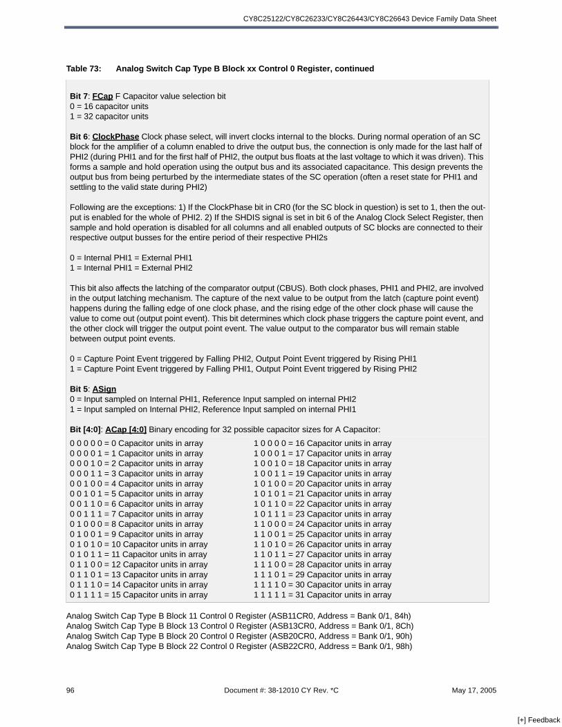
CY8C25122/CY8C26233/CY8C26443/CY8C26643 Device Family Data Sheet
Analog Switch Cap Type B Block 11 Control 0 Register (ASB11CR0, Address = Bank 0/1, 84h)Analog Switch Cap Type B Block 13 Control 0 Register (ASB13CR0, Address = Bank 0/1, 8Ch)Analog Switch Cap Type B Block 20 Control 0 Register (ASB20CR0, Address = Bank 0/1, 90h)Analog Switch Cap Type B Block 22 Control 0 Register (ASB22CR0, Address = Bank 0/1, 98h)
Bit 7: FCap F Capacitor value selection bit0 = 16 capacitor units1 = 32 capacitor units
Bit 6: ClockPhase Clock phase select, will invert clocks internal to the blocks. During normal operation of an SC block for the amplifier of a column enabled to drive the output bus, the connection is only made for the last half of PHI2 (during PHI1 and for the first half of PHI2, the output bus floats at the last voltage to which it was driven). This forms a sample and hold operation using the output bus and its associated capacitance. This design prevents the output bus from being perturbed by the intermediate states of the SC operation (often a reset state for PHI1 and settling to the valid state during PHI2)
Following are the exceptions: 1) If the ClockPhase bit in CR0 (for the SC block in question) is set to 1, then the out-put is enabled for the whole of PHI2. 2) If the SHDIS signal is set in bit 6 of the Analog Clock Select Register, then sample and hold operation is disabled for all columns and all enabled outputs of SC blocks are connected to their respective output busses for the entire period of their respective PHI2s
0 = Internal PHI1 = External PHI11 = Internal PHI1 = External PHI2
This bit also affects the latching of the comparator output (CBUS). Both clock phases, PHI1 and PHI2, are involved in the output latching mechanism. The capture of the next value to be output from the latch (capture point event) happens during the falling edge of one clock phase, and the rising edge of the other clock phase will cause the value to come out (output point event). This bit determines which clock phase triggers the capture point event, and the other clock will trigger the output point event. The value output to the comparator bus will remain stable between output point events.
0 = Capture Point Event triggered by Falling PHI2, Output Point Event triggered by Rising PHI11 = Capture Point Event triggered by Falling PHI1, Output Point Event triggered by Rising PHI2
Bit 5: ASign0 = Input sampled on Internal PHI1, Reference Input sampled on internal PHI21 = Input sampled on Internal PHI2, Reference Input sampled on internal PHI1
Bit [4:0]: ACap [4:0] Binary encoding for 32 possible capacitor sizes for A Capacitor:
0 0 0 0 0 = 0 Capacitor units in array0 0 0 0 1 = 1 Capacitor units in array0 0 0 1 0 = 2 Capacitor units in array0 0 0 1 1 = 3 Capacitor units in array0 0 1 0 0 = 4 Capacitor units in array0 0 1 0 1 = 5 Capacitor units in array0 0 1 1 0 = 6 Capacitor units in array0 0 1 1 1 = 7 Capacitor units in array0 1 0 0 0 = 8 Capacitor units in array0 1 0 0 1 = 9 Capacitor units in array0 1 0 1 0 = 10 Capacitor units in array0 1 0 1 1 = 11 Capacitor units in array0 1 1 0 0 = 12 Capacitor units in array0 1 1 0 1 = 13 Capacitor units in array0 1 1 1 0 = 14 Capacitor units in array0 1 1 1 1 = 15 Capacitor units in array
1 0 0 0 0 = 16 Capacitor units in array1 0 0 0 1 = 17 Capacitor units in array1 0 0 1 0 = 18 Capacitor units in array1 0 0 1 1 = 19 Capacitor units in array1 0 1 0 0 = 20 Capacitor units in array1 0 1 0 1 = 21 Capacitor units in array1 0 1 1 0 = 22 Capacitor units in array1 0 1 1 1 = 23 Capacitor units in array1 1 0 0 0 = 24 Capacitor units in array1 1 0 0 1 = 25 Capacitor units in array1 1 0 1 0 = 26 Capacitor units in array1 1 0 1 1 = 27 Capacitor units in array1 1 1 0 0 = 28 Capacitor units in array1 1 1 0 1 = 29 Capacitor units in array1 1 1 1 0 = 30 Capacitor units in array1 1 1 1 1 = 31 Capacitor units in array
Table 73: Analog Switch Cap Type B Block xx Control 0 Register, continued
96 Document #: 38-12010 CY Rev. *C May 17, 2005
[+] Feedback
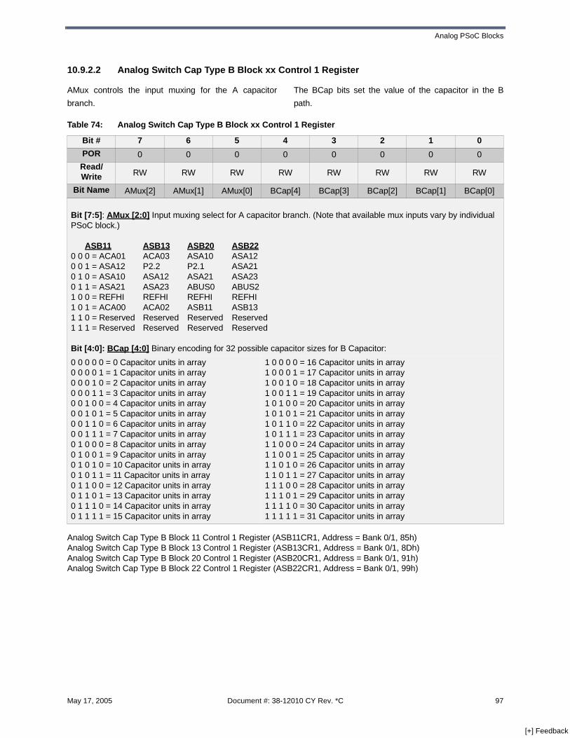
Analog PSoC Blocks
10.9.2.2 Analog Switch Cap Type B Block xx Control 1 Register
AMux controls the input muxing for the A capacitor
branch.
The BCap bits set the value of the capacitor in the B
path.
Analog Switch Cap Type B Block 11 Control 1 Register (ASB11CR1, Address = Bank 0/1, 85h)Analog Switch Cap Type B Block 13 Control 1 Register (ASB13CR1, Address = Bank 0/1, 8Dh)Analog Switch Cap Type B Block 20 Control 1 Register (ASB20CR1, Address = Bank 0/1, 91h)Analog Switch Cap Type B Block 22 Control 1 Register (ASB22CR1, Address = Bank 0/1, 99h)
Table 74: Analog Switch Cap Type B Block xx Control 1 Register
Bit # 7 6 5 4 3 2 1 0
POR 0 0 0 0 0 0 0 0Read/Write RW RW RW RW RW RW RW RW
Bit Name AMux[2] AMux[1] AMux[0] BCap[4] BCap[3] BCap[2] BCap[1] BCap[0]
Bit [7:5]: AMux [2:0] Input muxing select for A capacitor branch. (Note that available mux inputs vary by individual PSoC block.)
ASB11 ASB13 ASB20 ASB220 0 0 = ACA01 ACA03 ASA10 ASA120 0 1 = ASA12 P2.2 P2.1 ASA210 1 0 = ASA10 ASA12 ASA21 ASA230 1 1 = ASA21 ASA23 ABUS0 ABUS21 0 0 = REFHI REFHI REFHI REFHI1 0 1 = ACA00 ACA02 ASB11 ASB131 1 0 = Reserved Reserved Reserved Reserved1 1 1 = Reserved Reserved Reserved Reserved
Bit [4:0]: BCap [4:0] Binary encoding for 32 possible capacitor sizes for B Capacitor:
0 0 0 0 0 = 0 Capacitor units in array0 0 0 0 1 = 1 Capacitor units in array0 0 0 1 0 = 2 Capacitor units in array0 0 0 1 1 = 3 Capacitor units in array0 0 1 0 0 = 4 Capacitor units in array0 0 1 0 1 = 5 Capacitor units in array0 0 1 1 0 = 6 Capacitor units in array0 0 1 1 1 = 7 Capacitor units in array0 1 0 0 0 = 8 Capacitor units in array0 1 0 0 1 = 9 Capacitor units in array0 1 0 1 0 = 10 Capacitor units in array0 1 0 1 1 = 11 Capacitor units in array0 1 1 0 0 = 12 Capacitor units in array0 1 1 0 1 = 13 Capacitor units in array0 1 1 1 0 = 14 Capacitor units in array0 1 1 1 1 = 15 Capacitor units in array
1 0 0 0 0 = 16 Capacitor units in array1 0 0 0 1 = 17 Capacitor units in array1 0 0 1 0 = 18 Capacitor units in array1 0 0 1 1 = 19 Capacitor units in array1 0 1 0 0 = 20 Capacitor units in array1 0 1 0 1 = 21 Capacitor units in array1 0 1 1 0 = 22 Capacitor units in array1 0 1 1 1 = 23 Capacitor units in array1 1 0 0 0 = 24 Capacitor units in array1 1 0 0 1 = 25 Capacitor units in array1 1 0 1 0 = 26 Capacitor units in array1 1 0 1 1 = 27 Capacitor units in array1 1 1 0 0 = 28 Capacitor units in array1 1 1 0 1 = 29 Capacitor units in array1 1 1 1 0 = 30 Capacitor units in array1 1 1 1 1 = 31 Capacitor units in array
May 17, 2005 Document #: 38-12010 CY Rev. *C 97
[+] Feedback

CY8C25122/CY8C26233/CY8C26443/CY8C26643 Device Family Data Sheet
10.9.2.3 Analog Switch Cap Type B Block xx Control 2 Register
AnalogBus gates the output to the analog column bus.
The output on the analog column bus is affected by the
state of the ClockPhase bit in Control 0 Register
(ASB11CR0, ASB13CR0, ASB20CR0, ASB22CR0). If
AnalogBus is set to 0, the output to the analog column
bus is tri-stated. If AnalogBus is set to 1, the ClockPhase
bit selects the signal that is output to the analog-column
bus. If the ClockPhase bit is 0, the block output is gated
by sampling clock on last part of PHI2. If the ClockPhase
bit is 1, the block ClockPhase continuously drives the
analog column bus.
CompBus controls the output to the column comparator
bus. Note that if the comparator bus is not driven by any-
thing in the column, it is pulled low. The comparator out-
put is evaluated on the rising edge of internal PHI1 and
is latched so it is available during internal PHI2.
AutoZero controls the shorting of the output to the invert-
ing input of the op-amp. When shorted, the op-amp is
basically a follower. The output is the op-amp offset. By
using the feedback capacitor of the integrator, the block
can memorize the offset and create an offset cancella-
tion scheme. AutoZero also controls a pair of switches
between the A and B branches and the summing node of
the op-amp. If AutoZero is enabled, then the pair of
switches is active. AutoZero also affects the function of
the FSW1 bit in Control 3 Register.
The CCap bits set the value of the capacitor in the C
path.
98 Document #: 38-12010 CY Rev. *C May 17, 2005
[+] Feedback

Analog PSoC Blocks
Analog Switch Cap Type B Block 11 Control 2 Register (ASB11CR2, Address = Bank 0/1, 86h)Analog Switch Cap Type B Block 13 Control 2 Register (ASB13CR2, Address = Bank 0/1, 8Eh)Analog Switch Cap Type B Block 20 Control 2 Register (ASB20CR2, Address = Bank 0/1, 92h)Analog Switch Cap Type B Block 22 Control 2 Register (ASB22CR2, Address = Bank 0/1, 9Ah)
Table 75: Analog Switch Cap Type B Block xx Control 2 Register
Bit # 7 6 5 4 3 2 1 0
POR 0 0 0 0 0 0 0 0Read/Write RW RW RW RW RW RW RW RW
Bit Name AnalogBus CompBus AutoZero CCap[4] CCap[3] CCap[2] CCap[1] CCap[0]
Bit 7: AnalogBus Enable output to the analog bus0 = Disable output to analog column bus1 = Enable output to analog column bus (The output on the analog column bus is affected by the state of the ClockPhase bit in Control 0 Register (ASB11CR0, ASB13CR0, ASB20CR0, ASB22CR0). If AnalogBus is set to 0, the output to the analog column bus is tri-stated. If AnalogBus is set to 1, the ClockPhase bit selects the signal that is output to the analog column bus. If the ClockPhase bit is 0, the block output is gated by sampling clock on last part of PHI2. If the ClockPhase bit is 1, the block output continuously drives the analog column bus)
Bit 6: CompBus Enable output to the comparator bus0 = Disable output to comparator bus1 = Enable output to comparator bus
Bit 5: AutoZero Bit for controlling gated switches0 = Shorting switch is not active. Input cap branches shorted to op-amp input1 = Shorting switch is enabled during internal PHI1. Input cap branches shorted to analog ground during internal PHI1 and to op-amp input during internal PHI2.
Bit [4:0]: CCap [4:0] Binary encoding for 32 possible capacitor sizes for C Capacitor:
0 0 0 0 0 = 0 Capacitor units in array0 0 0 0 1 = 1 Capacitor units in array0 0 0 1 0 = 2 Capacitor units in array0 0 0 1 1 = 3 Capacitor units in array0 0 1 0 0 = 4 Capacitor units in array0 0 1 0 1 = 5 Capacitor units in array0 0 1 1 0 = 6 Capacitor units in array0 0 1 1 1 = 7 Capacitor units in array0 1 0 0 0 = 8 Capacitor units in array0 1 0 0 1 = 9 Capacitor units in array0 1 0 1 0 = 10 Capacitor units in array0 1 0 1 1 = 11 Capacitor units in array0 1 1 0 0 = 12 Capacitor units in array0 1 1 0 1 = 13 Capacitor units in array0 1 1 1 0 = 14 Capacitor units in array0 1 1 1 1 = 15 Capacitor units in array
1 0 0 0 0 = 16 Capacitor units in array1 0 0 0 1 = 17 Capacitor units in array1 0 0 1 0 = 18 Capacitor units in array1 0 0 1 1 = 19 Capacitor units in array1 0 1 0 0 = 20 Capacitor units in array1 0 1 0 1 = 21 Capacitor units in array1 0 1 1 0 = 22 Capacitor units in array1 0 1 1 1 = 23 Capacitor units in array1 1 0 0 0 = 24 Capacitor units in array1 1 0 0 1 = 25 Capacitor units in array1 1 0 1 0 = 26 Capacitor units in array1 1 0 1 1 = 27 Capacitor units in array1 1 1 0 0 = 28 Capacitor units in array1 1 1 0 1 = 29 Capacitor units in array1 1 1 1 0 = 30 Capacitor units in array1 1 1 1 1 = 31 Capacitor units in array
May 17, 2005 Document #: 38-12010 CY Rev. *C 99
[+] Feedback

CY8C25122/CY8C26233/CY8C26443/CY8C26643 Device Family Data Sheet
10.9.2.4 Analog Switch Cap Type B Block xx Control 3 Register
ARefMux selects the reference input of the A capacitorbranch.
FSW1 is used to control a switch in the integrator capac-itor path. It connects the output of the op-amp to the inte-grating cap. The state of the switch is affected by thestate of the AutoZero bit in Control 2 Register(ASB11CR2, ASB13CR2, ASB20CR2, ASB22CR2). Ifthe FSW1 bit is set to 0, the switch is always disabled. Ifthe FSW1 bit is set to 1, the AutoZero bit determines thestate of the switch. If the AutoZero bit is 0, the switch isenabled at all times. If the AutoZero bit is 1, the switch isenabled only when the internal PHI2 is high.
FSW0 is used to control a switch in the integrator capac-itor path. It connects the output of the op-amp to analogground.
BSW is used to control switching in the B branch. If dis-abled, the B capacitor branch is a continuous timebranch like the C branch of the SC A Block. If enabled,then on internal PHI1, both ends of the cap are switchedto analog ground. On internal PHI2, one end is switchedto the B input and the other end is switched to the sum-ming node.
BMuxSCB controls muxing to the input of the B capacitorbranch. The B branch can be switched or unswitched.
Analog Switch Cap Type B Block 11 Control 3 Register (ASB11CR3, Address = Bank 0/1, 87h)Analog Switch Cap Type B Block 13 Control 3 Register (ASB13CR3, Address = Bank 0/1, 8Fh)Analog Switch Cap Type B Block 20 Control 3 Register (ASB20CR3, Address = Bank 0/1, 93h)Analog Switch Cap Type B Block 22 Control 3 Register (ASB22CR3, Address = Bank 0/1, 9Bh)
Table 76: Analog Switch Cap Type B Block xx Control 3 Register
Bit # 7 6 5 4 3 2 1 0POR 0 0 0 0 0 0 0 0Read/Write RW RW RW RW RW RW RW RW
Bit Name ARefMux[1] ARefMux[0] FSW[1] FSW[0] BSW BMuxSCB Power[1] Power[0]
Bit [7:6]: ARefMux [1:0] Encoding for selecting reference input0 0 = Analog ground is selected0 1 = REFHI input selected (This is usually the high reference)1 0 = REFLO input selected (This is usually the low reference)1 1 = Reference selection is driven by the comparator (When output comparator node is set high, the input is set to REFHI. When set low, the input is set to REFLO)
Bit 5: FSW1 Bit for controlling gated switches0 = Switch is disabledFSW1 bit is set to 1; the state of the switch is determined by the AutoZero bit. If the AutoZero bit is 0, the switch is enabled at all times. If the AutoZero bit is 1, the switch is enabled only when the internal PHI2 is high
Bit 4: FSW0 Bits for controlling gated switches0 = Switch is disabled1 = Switch is enabled when PHI1 is high
Bit 3: BSW Enable switching in branch0 = B branch is a continuous time path1 = B branch is switched with internal PHI2 sampling
Bit 2: BMuxSCB Encoding for selecting B inputs. (Note that the available mux inputs vary by individual PSoC block)ASB11 ASB13 ASB20 ASB22
0 = ACA00 ACA02 ASB11 ASB131 = ACA01 ACA03 ASA10 ASA12
Bit [1:0]: Power [1:0] Encoding for selecting 1 of 4 power levels0 0 = Off0 1 = 10 µA, typical1 0 = 50 µA, typical1 1 = 200 µA, typical
100 Document #: 38-12010 CY Rev. *C May 17, 2005
[+] Feedback
Analog PSoC Blocks
10.10 Analog Comparator Bus
Each analog column has a dedicated comparator bus
associated with it. Every analog PSoC block has a com-
parator output that can drive out on this bus, but the
comparator output from only one analog block in a col-
umn can be actively driving the comparator bus for that
column at any one time. The output on the comparator
bus can drive into the digital blocks, and is also available
to be read in the Analog Comparator Control Register
(CMP_CR, Address = Bank 0,64H).
The comparator bus is latched before it is available to
either drive the digital blocks, or be read in the Analog
Comparator Control Register. The latch for each compar-
ator bus is transparent (the output tracks the input) dur-
ing the high period of PHI2. During the low period of
PHI2 the latch retains the value on the comparator bus
during the high to low transition of PHI2.
The output from the analog block that is actively driving
the bus may also be latched internal to the analog block
itself.
In the Continuous Time analog blocks, the CPhase and
CLatch bits inside the Analog Continuous Time Type A
Block xx Control Register 2 determine whether the out-
put signal on the comparator bus is latched inside the
block, and if it is, which clock phase it is latched on.
In the Switched Capacitor analog blocks, the output on
the comparator bus is always latched. The ClockPhase
bit in the Analog SwitchCap Type A Block xx Control
Register 0 or the Analog SwitchCap Type B Block xx
Control Register 0 determines the phase on which this
data is latched and available.
Analog Comparator Control Register (CMP_CR, Address = Bank 0, 64h)
10.11 Analog Synchronization
For high precision analog operation, it may be necessary
to precisely time when updated register values are avail-
able to the analog PSOC blocks. The optimum time to
update values in Switch Cap registers is at the beginning
of the PHI1 active period. The SYNCEN bit in the Analog
Synchronization Control Register is designed to address
this. (The AINT bits of the Analog Comparator Register
(CMP_CR) are another way to address it with interrupts.)
When the SYNCEN bit is set, a subsequent write instruc-
tion to any register in a Switch Cap block will cause the
CPU to stall until the rising edge of PHI1. This mode is in
effect until the SYNCEN bit is cleared.
Table 77: Analog Comparator Control Register
Bit # 7 6 5 4 3 2 1 0
POR 0 0 0 0 0 0 0 0Read/Write R R R R RW RW RW RW
Bit Name COMP 3 COMP 2 COMP 1 COMP 0 AINT 3 AINT 2 AINT 1 AINT 0
Bit 7: COMP 3 COMP 3 bit [0] indicates the state of the analog comparator bus for the Analog Column xBit 6: COMP 2 COMP 2 bit [0] indicates the state of the analog comparator bus for the Analog Column xBit 5: COMP 1 COMP 1 bit [0] indicates the state of the analog comparator bus for the Analog Column xBit 4: COMP 0 COMP 0 bit [0] indicates the state of the analog comparator bus for the Analog Column x
Bit 3: AINT 3 AINT 3 bit [0] or [1] (as defined below) selects the Analog Interrupt Source for the Analog Column xBit 2: AINT 2 AINT 2 bit [0] or [1] (as defined below) selects the Analog Interrupt Source for the Analog Column xBit 1: AINT 1 AINT 1 bit [0] or [1] (as defined below) selects the Analog Interrupt Source for the Analog Column xBit 0: AINT 0 AINT 0 bit [0] or [1] (as defined below) selects the Analog Interrupt Source for the Analog Column x
0 = Comparator bus1 = PHI2 (Falling edge of PHI2 causes an interrupt)
May 17, 2005 Document #: 38-12010 CY Rev. *C 101
[+] Feedback
CY8C25122/CY8C26233/CY8C26443/CY8C26643 Device Family Data Sheet
The SAR hardware accelerator is a block of specialized
hardware designed to sequence the SAR algorithm for
efficient A/D conversion. A SAR ADC is implemented
conceptually with a DAC of the desired precision, and a
comparator. This functionality can be configured from
one or more PSoC blocks. For each conversion, the firm-
ware should initialize the ASY_CR register as defined
below, and set the sign bit of the DAC as the first guess
in the algorithm. A sequence of OR instructions (Read,
Modify, Write) to the DAC (CR0) register is then exe-
cuted. Each of these OR instructions causes the SAR
hardware to read the current state of the comparator,
checking the validity of the previous guess. It either
clears it or leaves it set, accordingly. The next LSB in the
DAC register is also set as the next guess. Six OR
instructions will complete the conversion of a 6-bit DAC.
The resulting DAC code, which matches the input volt-
age to within 1 LSB, is then read back from the DAC
CR0 register.
10.11.1 Analog Stall and Analog Stall Lockup
Stall lockup affects the operation of stalled IO writes,
such as DAC writes and the stalled IOR of the SAR hard-
ware accelerator. The DAC and SAR User Modules
operate in this mode. The analog column clock fre-
quency must not be a power of two multiple (2, 4, 8...)
higher than the CPU clock frequency. Under this condi-
tion, the CPU will never recover from a stall.
See the list of relationships (in MHz) that will fail:
You can still run the CPU clock slower than the column
clock if the relationship is not a power of two multiple.
For example, you can run at 0.6 MHz, which is not a
power of two multiple of any CPU frequency and there-
fore any CPU frequency can be selected. If the CPU fre-
quency is greater than or equal to the analog column
clock, there is not a problem.
Analog Synchronization Control Register (ASY_CR, Address = Bank 0, 65h)
Table 78: Analog Frequency Relationships
Analog Column Clock CPU Clock
3. 1.5, 0.75, .018, 0.093
1.5 0.75, 0.18, 0.093
0.75 0.18, 0.093
0.37 0.18, 0.093
0.18 0.093
Table 79: Analog Synchronization Control Register
Bit # 7 6 5 4 3 2 1 0
POR 0 0 0 0 0 0 0 0Read/Write -- W W W RW RW RW RW
Bit Name ReservedSARCOUNT
[2]SARCOUNT
[1]SARCOUNT
[0]SAR-SIGN
SARCOL [1]
SARCOL [0]
SYN-CEN
Bit 7: Reserved
Bit [6:4]: SARCOUNT [2:0] Initial SAR count. Load this field with the number of bits to process. In a typical 6-bit SAR, the value would be 6
Bit 3: SARSIGN Adjust the SAR comparator based on the type of block addressed. In a DAC configuration with more than one PSoC block (more than 6-bits), this bit would be 0 when processing the most significant block and 1 when processing the least significant block. This is because the least significant block of a DAC is an inverting input to the most significant block
Bit [2:1]: SARCOL [1:0] Column select for SAR comparator input. The DAC portion of the SAR can reside in any of the appropriate positions in the analog PSOC block array. However, once the comparator block is positioned (and it is possible to have the DAC and comparator in the same block), this should be the column selected
Bit 0: SYNCEN Set to 1, will stall the CPU until the rising edge of PHI1, if a write to a register within an analog Switch Cap block takes place
102 Document #: 38-12010 CY Rev. *C May 17, 2005
[+] Feedback
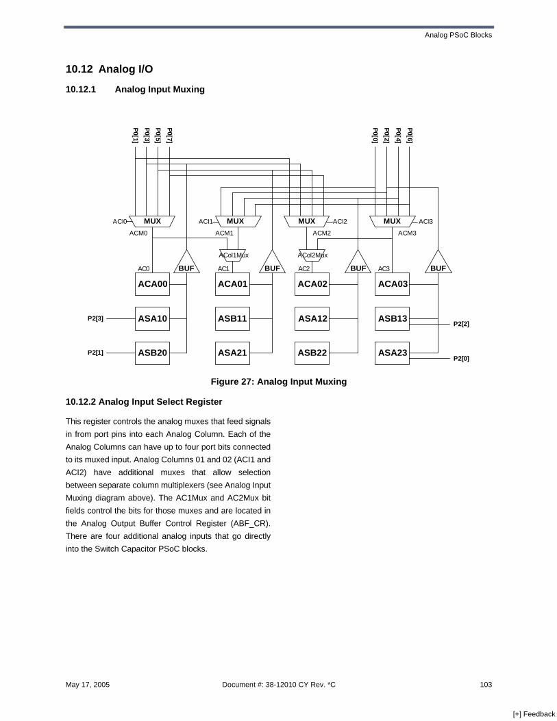
Analog PSoC Blocks
10.12 Analog I/O
10.12.1 Analog Input Muxing
10.12.2 Analog Input Select Register
This register controls the analog muxes that feed signals
in from port pins into each Analog Column. Each of the
Analog Columns can have up to four port bits connected
to its muxed input. Analog Columns 01 and 02 (ACI1 and
ACI2) have additional muxes that allow selection
between separate column multiplexers (see Analog Input
Muxing diagram above). The AC1Mux and AC2Mux bit
fields control the bits for those muxes and are located in
the Analog Output Buffer Control Register (ABF_CR).
There are four additional analog inputs that go directly
into the Switch Capacitor PSoC blocks.
Figure 27: Analog Input Muxing
P2[0]
P2[2]
P2[1]
P2[3]
ACA00 ACA03ACA02ACA01
ASA10
ASA23
ASA12
ASA21ASB20
ASB13
ASB22
ASB11
MUX MUXMUXMUX
BUF BUF BUF BUF
P0[0]
P0[2]
P0[4]
P0[6]
P0[1]
P0[3]
P0[5]
P0[7]
ACI0 ACI1 ACI2 ACI3
ACM0 ACM1 ACM2 ACM3
AC0 AC1 AC2 AC3
ACol1Mux ACol2Mux
May 17, 2005 Document #: 38-12010 CY Rev. *C 103
[+] Feedback
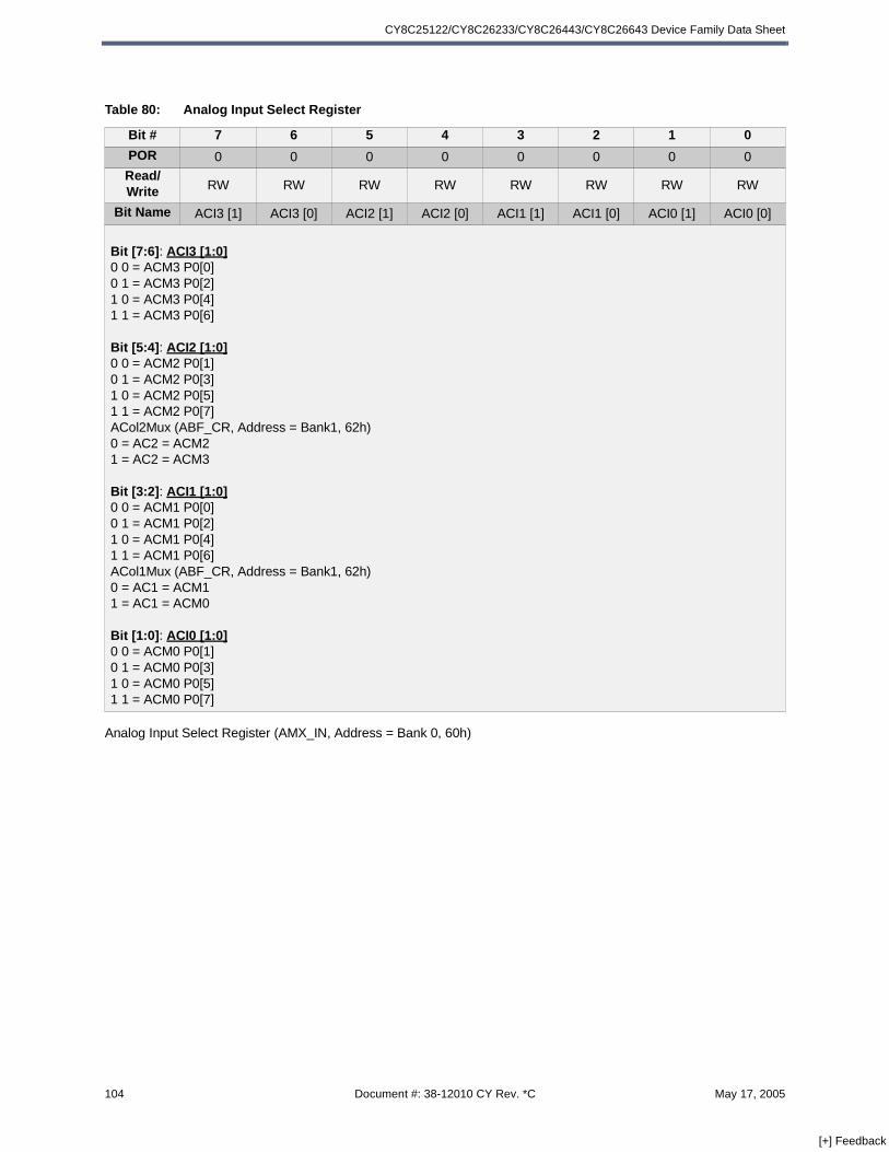
CY8C25122/CY8C26233/CY8C26443/CY8C26643 Device Family Data Sheet
Table 80: Analog Input Select Register
Analog Input Select Register (AMX_IN, Address = Bank 0, 60h)
Bit # 7 6 5 4 3 2 1 0
POR 0 0 0 0 0 0 0 0Read/Write RW RW RW RW RW RW RW RW
Bit Name ACI3 [1] ACI3 [0] ACI2 [1] ACI2 [0] ACI1 [1] ACI1 [0] ACI0 [1] ACI0 [0]
Bit [7:6]: ACI3 [1:0]0 0 = ACM3 P0[0]0 1 = ACM3 P0[2]1 0 = ACM3 P0[4]1 1 = ACM3 P0[6]
Bit [5:4]: ACI2 [1:0]0 0 = ACM2 P0[1] 0 1 = ACM2 P0[3] 1 0 = ACM2 P0[5]1 1 = ACM2 P0[7]ACol2Mux (ABF_CR, Address = Bank1, 62h)0 = AC2 = ACM21 = AC2 = ACM3 Bit [3:2]: ACI1 [1:0]0 0 = ACM1 P0[0] 0 1 = ACM1 P0[2] 1 0 = ACM1 P0[4]1 1 = ACM1 P0[6]ACol1Mux (ABF_CR, Address = Bank1, 62h)0 = AC1 = ACM11 = AC1 = ACM0
Bit [1:0]: ACI0 [1:0]0 0 = ACM0 P0[1]0 1 = ACM0 P0[3]1 0 = ACM0 P0[5]1 1 = ACM0 P0[7]
104 Document #: 38-12010 CY Rev. *C May 17, 2005
[+] Feedback
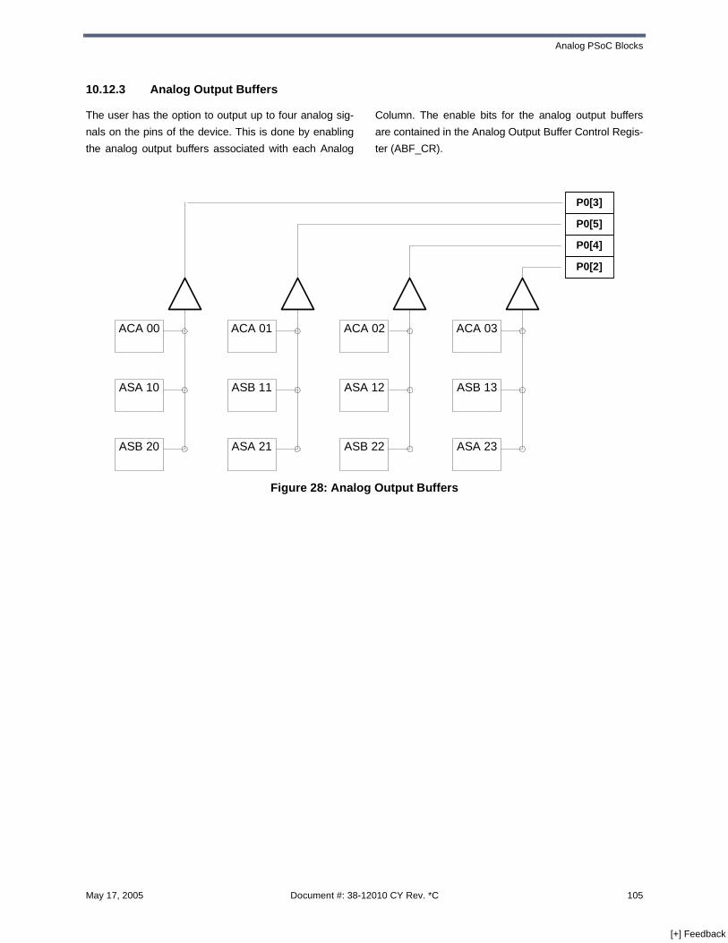
Analog PSoC Blocks
10.12.3 Analog Output Buffers
The user has the option to output up to four analog sig-
nals on the pins of the device. This is done by enabling
the analog output buffers associated with each Analog
Column. The enable bits for the analog output buffers
are contained in the Analog Output Buffer Control Regis-
ter (ABF_CR).
Figure 28: Analog Output Buffers
ASA 23
ASB 13
ACA 03
ASB 22
ASA 12
ACA 02
ASA 21
ASB 11
ACA 01
ASB 20
ASA 10
ACA 00
P0[3]
P0[5]
P0[4]
P0[2]
May 17, 2005 Document #: 38-12010 CY Rev. *C 105
[+] Feedback

CY8C25122/CY8C26233/CY8C26443/CY8C26643 Device Family Data Sheet
10.12.4 Analog Output Buffer Control Register
Analog Output Buffer Control Register (ABF_CR, Address = Bank 1, 62h)
10.13 Analog Modulator
The user has the capability to use the Analog SwitchCap Type A PSoC Blocks in Columns 0 and 2 as ampli-tude modulators. The Analog Modulator Control Register(AMD_CR) allows the user to select the appropriatemodulating signal. When the modulating signal is low,the polarity follows the setting of the ASign bit set in theAnalog Switch Cap Type A Control 0 Register(ASAxxCR0). When this signal is high, the normal gainpolarity of the PSoC block is inverted.
Table 81: Analog Output Buffer Control Register
Bit # 7 6 5 4 3 2 1 0
POR 0 0 0 0 0 0 0 0Read/Write W W W W W W -- W
Bit Name ACol1Mux ACol2Mux ABUF1EN ABUF2EN ABUF0EN ABUF3EN Reserved PWR
Bit 7: ACol1Mux0 = Set column 1 input to column 1 input mux output1 = Set column 1 input to column 0 input mux output
Bit 6: ACol2Mux0 = Set column 2 input to column 2 input mux output1 = Set column 2 input to column 3 input mux output
Bit 5: ABUF1EN Enables the analog output buffer for Analog Column 1 (Pin P0[5])0 = Disable analog output buffer1 = Enable analog output buffer
Bit 4: ABUF2EN Enables the analog output buffer for Analog Column 2 (Pin P0[4])0 = Disable analog output buffer1 = Enable analog output buffer
Bit 3: ABUF0EN Enables the analog output buffer for Analog Column 0 (Pin P0[3])0 = Disable analog output buffer1 = Enable analog output buffer
Bit 2: ABUF3EN Enables the analog output buffer for Analog Column 3 (Pin P0[2])0 = Disable analog output buffer1 = Enable analog output buffer
Bit [1]: Reserved Must be left as 0
Bit [0]: PWR Determines power level of all output buffers0 = Low output power1 = High output power
106 Document #: 38-12010 CY Rev. *C May 17, 2005
[+] Feedback

Analog PSoC Blocks
Analog Modulator Control Register (AMD_CR, Address = Bank 1, 63h)
10.14 Analog PSoC Block Functionality
The analog PSoC blocks can be used to implement a
wide range of functions, limited only by the designer’s
imagination. The following functions operate within the
capability of the analog PSoC blocks using one analog
PSoC block, multiple analog blocks, a combination of
more than one type of analog block, or a combination of
analog and digital PSoC blocks. Most of these functions
are currently available as User Modules in PSoC
Designer. Others will be added in the future.
Delta-Sigma A/D Converters
Successive Approximation A/D Converters
Incremental A/D Converters
Programmable Gain/Loss Stage
Analog Comparators
Zero-Crossing Detectors
Low-Pass Filter
Band-Pass Filter
Notch Filter
Amplitude Modulators
Amplitude Demodulators
Sine-Wave Generators
Sine-Wave Detectors
Sideband Detection
Sideband Stripping
Audio Output Drive
DTMF Generator
FSK Modulator
By modifying registers, as described in this Data Sheet,
users can configure PSoC blocks to perform these func-
tions and more.
Table 82: Analog Modulator Control Register
Bit # 7 6 5 4 3 2 1 0
POR 0 0 0 0 0 0 0 0Read/Write RW RW RW RW RW RW RW RW
Bit Name Reserved Reserved Reserved Reserved AMOD2[1] AMOD2[0] AMOD0[1] AMOD0[0]
Bit 7: ReservedBit 6: ReservedBit 5: ReservedBit 4: Reserved
Bit [3:2]: AMOD2[1], AMOD2[0] Selects the modulation signal for Analog Column 20 0 = No Modulation0 1 = Global Output [0]1 0 = Global Output [4]1 1 = Digital Basic Type A Block 03
Bit [1:0]: AMOD0[1], AMOD0[0] Selects the modulation signal for Analog Column 00 0 = No Modulation0 1 = Global Output [0]1 0 = Global Output [4]1 1 = Digital Basic Type A Block 03
May 17, 2005 Document #: 38-12010 CY Rev. *C 107
[+] Feedback

CY8C25122/CY8C26233/CY8C26443/CY8C26643 Device Family Data Sheet
10.15 Temperature Sensing Capability
A temperature-sensitive voltage derived from the Band
Gap sensing on the die is buffered and available as an
analog input into the Analog Switch Cap Type A Block
ASA21. Temperature sensing allows protection of device
operating ranges for fail-safe applications. Temperature
sensing combined with a long sleep timer interval (to
allow the die to approximate ambient temperature) can
give an approximate ambient temperature for data acqui-
sition and battery charging applications. The user may
also calibrate the internal temperature rise based on a
known current consumption.
The temperature sensor input to the ASA21 block is
labeled VTemp, and its associated ground reference is
labeled TRefGND (see Figure 22:, Figure 24:).
108 Document #: 38-12010 CY Rev. *C May 17, 2005
[+] Feedback

Special Features of the CPU
11.0 Special Features of the CPU
11.1 Multiplier/Accumulator
A fast, on-chip signed 2’s complement MAC (Multiply/
Accumulate) function is provided to assist the main CPU
with digital signal processing applications. Multiply
results, as well as the lower 2 bytes of the Accumulator,
are available immediately after the input registers are
written. The upper 2 bytes require a single instruction
delay before reading. The MAC function is tied directly
on the internal data bus, and is mapped into the register
space. The following MAC block diagram provides data
flow information. The user has the choice to either cause
a multiply/accumulate function to take place, or a multi-
ply only function. The user selects which operation is
performed by the choice of input register. The multiply
function occurs immediately whenever the MUL_X or the
MUL_Y multiplier input registers are written, and the
result is available in the MUL_DH and MUL_DL multiplier
result registers. The Multiply/Accumulate function is exe-
cuted whenever there is a write to the MAC_X or the
MAC_Y Multiply/Accumulate input registers, and the
result is available in the ACC_DR3, ACC_DR2,
ACC_DR1, and ACC_DR0 accumulator result registers.
A write to MUL_X or MAC_X is input as the X value to
both the multiply and Multiply/Accumulate functions. A
write to MUL_Y or MAC_Y is input as the Y value to both
the multiply and Multiply/Accumulate functions. A write to
the MAC_CL0 or MAC_CL1 registers will clear the value
in the four accumulate registers.
Operation of the Multiply/Accumulate function relies on
proper multiplicand input. The first value of each multipli-
cand must be placed into MUL_X (or MUL_Y) register to
avoid causing a Multiply/Accumulate to occur. The sec-
ond multiplicand must be placed into MAC_Y (or
MAC_X) thereby triggering the Multiply/Accumulate
function.
MUL_X, MUL_Y, MAC_X, and MAC_Y are 8-bit signed
input registers. MUL_DL and MUL_DH form a 16-bit
signed output. ACC_DR0, ACC_DR1, ACC_DR2 and
ACC_DR3 form a 32-bit signed output.
An extra instruction must be inserted between the follow-
ing sequences of MAC operations to provide extra delay.
If this is not done, the Accumulator results will be inaccu-
rate.
a. Two MAC instructions in succession:
mov reg[MAC_X],anop //add nop or any other instructionmov reg[MAC_X],a
For sequence a., there is no workaround, the nop or
other instruction must be inserted.
b. A MAC instruction followed by a read of the most significant Accumulator bytes:
mov reg[MAC_X],anop //add nop or any other instructionmov a,[ACC_DR2] // or ACC_DR3
For sequence b., the least significant Accumulator bytes
(ACC_DR0, ACC_DR1) may be reliably read directly
after the MAC instruction.
Writing to the multiplier registers (MUL_X, MUL_Y), and
reading the result back from the multiplier product regis-
ters (MUL_DH, MUL_DL), is not affected by this problem
and does not have any restrictions.
May 17, 2005 Document #: 38-12010 CY Rev. *C 109
[+] Feedback

CY8C25122/CY8C26233/CY8C26443/CY8C26643 Device Family Data Sheet
Multiply Input X Register (MUL_X, Address = Bank 0, E8h)
Multiply Input Y Register (MUL_Y, Address = Bank 0, E9h)
Figure 29: Multiply/Accumulate Block Diagram
Table 83: Multiply Input X Register
Bit # 7 6 5 4 3 2 1 0
POR 0 0 0 0 0 0 0 0
Read/Write W W W W W W W W
Name Data [7] Data [6] Data [5] Data [4] Data [3] Data [2] Data [1] Data [0]
Bit [7:0]: Data [7:0] 8-bit data is the input value for X multiplier
Table 84: Multiply Input Y Register
Bit # 7 6 5 4 3 2 1 0
POR 0 0 0 0 0 0 0 0
Read/Write W W W W W W W W
Bit Name Data [7] Data [6] Data [5] Data [4] Data [3] Data [2] Data [1] Data [0]
Bit [7:0]: Data [7:0] 8-bit data is the input value for Y multiplier
MULTIPLIER Z out, 16 BIT
32-BITACCUMULATOR
32-BIT ACC
16 BIT
ToInternalSystem
Bus
MUL_Y or MAC_Y
MUL_X or MAC_X
A CC_DR0
A CC_DR1
A CC_DR2
A CC_DR3
MUL_DL
MUL_DH
MAC_CL0
MAC_CL1
110 Document #: 38-12010 CY Rev. *C May 17, 2005
[+] Feedback
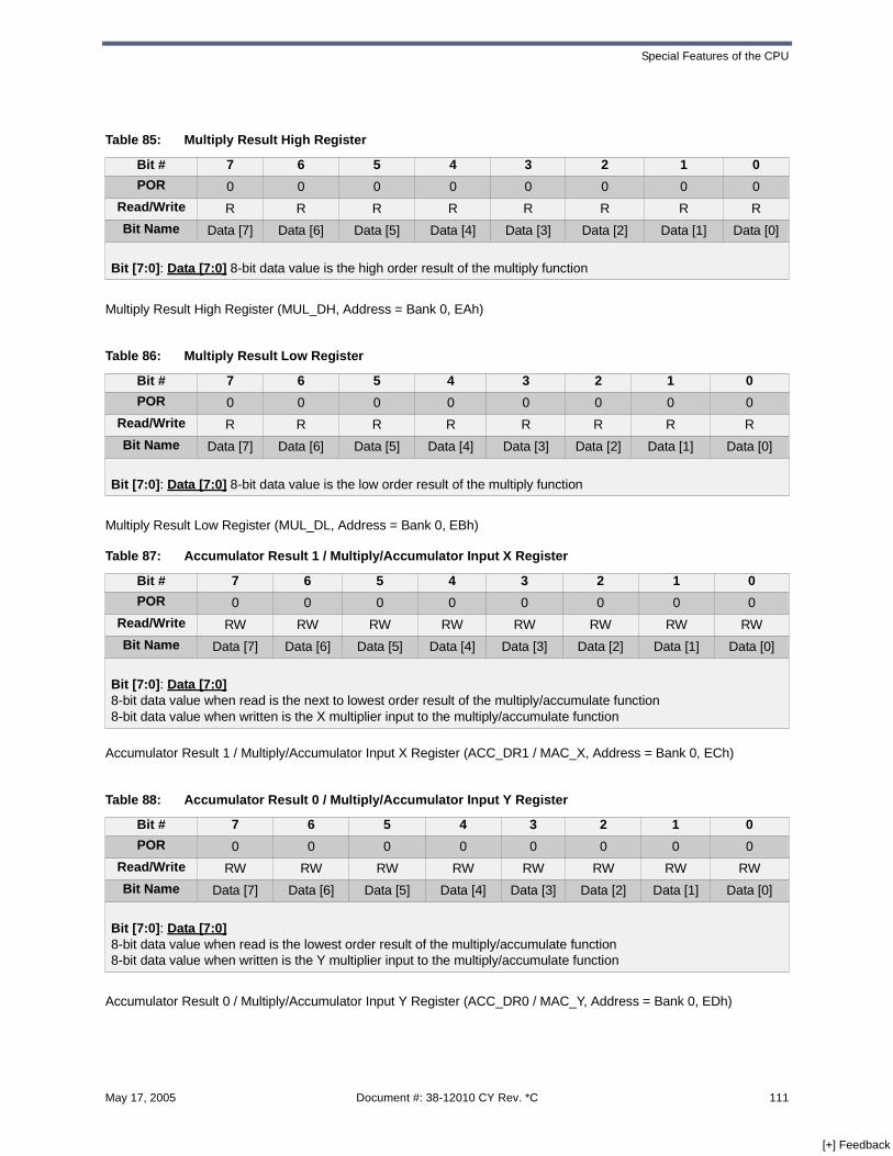
Special Features of the CPU
Multiply Result High Register (MUL_DH, Address = Bank 0, EAh)
Multiply Result Low Register (MUL_DL, Address = Bank 0, EBh)
Accumulator Result 1 / Multiply/Accumulator Input X Register (ACC_DR1 / MAC_X, Address = Bank 0, ECh)
Accumulator Result 0 / Multiply/Accumulator Input Y Register (ACC_DR0 / MAC_Y, Address = Bank 0, EDh)
Table 85: Multiply Result High Register
Bit # 7 6 5 4 3 2 1 0
POR 0 0 0 0 0 0 0 0
Read/Write R R R R R R R R
Bit Name Data [7] Data [6] Data [5] Data [4] Data [3] Data [2] Data [1] Data [0]
Bit [7:0]: Data [7:0] 8-bit data value is the high order result of the multiply function
Table 86: Multiply Result Low Register
Bit # 7 6 5 4 3 2 1 0
POR 0 0 0 0 0 0 0 0
Read/Write R R R R R R R R
Bit Name Data [7] Data [6] Data [5] Data [4] Data [3] Data [2] Data [1] Data [0]
Bit [7:0]: Data [7:0] 8-bit data value is the low order result of the multiply function
Table 87: Accumulator Result 1 / Multiply/Accumulator Input X Register
Bit # 7 6 5 4 3 2 1 0
POR 0 0 0 0 0 0 0 0
Read/Write RW RW RW RW RW RW RW RW
Bit Name Data [7] Data [6] Data [5] Data [4] Data [3] Data [2] Data [1] Data [0]
Bit [7:0]: Data [7:0]8-bit data value when read is the next to lowest order result of the multiply/accumulate function8-bit data value when written is the X multiplier input to the multiply/accumulate function
Table 88: Accumulator Result 0 / Multiply/Accumulator Input Y Register
Bit # 7 6 5 4 3 2 1 0
POR 0 0 0 0 0 0 0 0
Read/Write RW RW RW RW RW RW RW RW
Bit Name Data [7] Data [6] Data [5] Data [4] Data [3] Data [2] Data [1] Data [0]
Bit [7:0]: Data [7:0]8-bit data value when read is the lowest order result of the multiply/accumulate function8-bit data value when written is the Y multiplier input to the multiply/accumulate function
May 17, 2005 Document #: 38-12010 CY Rev. *C 111
[+] Feedback

CY8C25122/CY8C26233/CY8C26443/CY8C26643 Device Family Data Sheet
Accumulator Result 3 / Multiply/Accumulator Clear 0 Register (ACC_DR3 / MAC_CL0, Address = Bank 0, EEh)
Accumulator Result 2 / Multiply/Accumulator Clear 1 Register (ACC_DR2 / MAC_CL1, Address = Bank 0, EFh)
11.2 Decimator
The output of a ∆−Σ modulator is a high-speed, single bit
A/D converter. A single bit A/D converter is of little use to
anyone and must be converted to a lower speed multiple
bit output. Converting this high-speed single bit data
stream to a lower speed multiple bit data stream requires
a data decimator.
A “divide by n” decimator is a digital filter that takes the
single bit data at a fast rate and outputs multiple bits at
one nth the speed. For a single stage ∆−Σ converter, the
optimal filter has a sinc2 response. This filter can be
implemented as a finite impulse response (FIR) filter and
for a “divide by n” implementation should have the follow-
ing coefficients:
Table 89: Accumulator Result 3 / Multiply/Accumulator Clear 0 Register
Bit # 7 6 5 4 3 2 1 0
POR 0 0 0 0 0 0 0 0
Read/Write RW RW RW RW RW RW RW RW
Bit Name Data [7] Data [6] Data [5] Data [4] Data [3] Data [2] Data [1] Data [0]
Bit [7:0]: Data [7:0]8-bit data value when read is the highest order result of the multiply/accumulate functionAny 8-bit data value when written will cause all four Accumulator result registers to clear
Table 90: Accumulator Result 2 / Multiply/Accumulator Clear 1 Register
Bit # 7 6 5 4 3 2 1 0
POR 0 0 0 0 0 0 0 0
Read/Write RW RW RW RW RW RW RW RW
Bit Name Data [7] Data [6] Data [5] Data [4] Data [3] Data [2] Data [1] Data [0]
Bit [7:0]: Data [7:0]8-bit data value when read is next to highest order result of the multiply/accumulate functionAny 8-bit data value when written will cause all four Accumulator result registers to clear
Figure 30: Decimator Coefficients
0
n
Coeff
t
0 n-1 2n-1
112 Document #: 38-12010 CY Rev. *C May 17, 2005
[+] Feedback
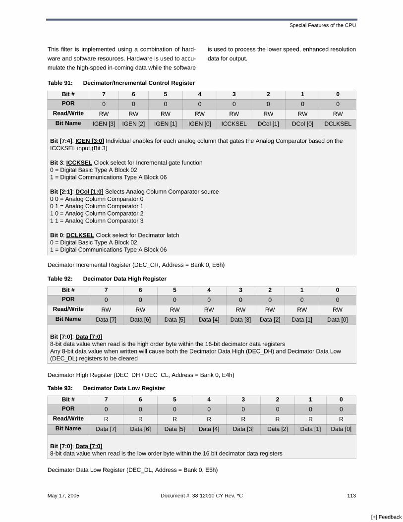
Special Features of the CPU
This filter is implemented using a combination of hard-
ware and software resources. Hardware is used to accu-
mulate the high-speed in-coming data while the software
is used to process the lower speed, enhanced resolution
data for output.
Decimator Incremental Register (DEC_CR, Address = Bank 0, E6h)
Decimator High Register (DEC_DH / DEC_CL, Address = Bank 0, E4h)
Decimator Data Low Register (DEC_DL, Address = Bank 0, E5h)
Table 91: Decimator/Incremental Control Register
Bit # 7 6 5 4 3 2 1 0
POR 0 0 0 0 0 0 0 0
Read/Write RW RW RW RW RW RW RW RW
Bit Name IGEN [3] IGEN [2] IGEN [1] IGEN [0] ICCKSEL DCol [1] DCol [0] DCLKSEL
Bit [7:4]: IGEN [3:0] Individual enables for each analog column that gates the Analog Comparator based on the ICCKSEL input (Bit 3)
Bit 3: ICCKSEL Clock select for Incremental gate function0 = Digital Basic Type A Block 021 = Digital Communications Type A Block 06
Bit [2:1]: DCol [1:0] Selects Analog Column Comparator source0 0 = Analog Column Comparator 00 1 = Analog Column Comparator 11 0 = Analog Column Comparator 21 1 = Analog Column Comparator 3
Bit 0: DCLKSEL Clock select for Decimator latch0 = Digital Basic Type A Block 021 = Digital Communications Type A Block 06
Table 92: Decimator Data High Register
Bit # 7 6 5 4 3 2 1 0
POR 0 0 0 0 0 0 0 0
Read/Write RW RW RW RW RW RW RW RW
Bit Name Data [7] Data [6] Data [5] Data [4] Data [3] Data [2] Data [1] Data [0]
Bit [7:0]: Data [7:0]8-bit data value when read is the high order byte within the 16-bit decimator data registersAny 8-bit data value when written will cause both the Decimator Data High (DEC_DH) and Decimator Data Low (DEC_DL) registers to be cleared
Table 93: Decimator Data Low Register
Bit # 7 6 5 4 3 2 1 0
POR 0 0 0 0 0 0 0 0
Read/Write R R R R R R R R
Bit Name Data [7] Data [6] Data [5] Data [4] Data [3] Data [2] Data [1] Data [0]
Bit [7:0]: Data [7:0]8-bit data value when read is the low order byte within the 16 bit decimator data registers
May 17, 2005 Document #: 38-12010 CY Rev. *C 113
[+] Feedback

CY8C25122/CY8C26233/CY8C26443/CY8C26643 Device Family Data Sheet
11.3 Reset
11.3.1 Overview
The microcontroller supports two types of resets. When
reset is initiated, all registers are restored to their default
states and all interrupts are disabled.
Reset Types: Power On Reset (POR), External Reset
(Xres), and Watchdog Reset (WDR).
The occurrence of a reset is recorded in the Status and
Control Register (CPU_SCR). Bits within this register
record the occurrence of POR and WDR Reset respec-
tively. The firmware can interrogate these bits to deter-
mine the cause of a reset.
The microcontroller resumes execution from ROM
address 0x0000 after a reset. The internal clocking mode
is active after a reset, until changed by user firmware. In
addition, the Sleep / Watchdog Timer is reset to its mini-
mum interval count.
Important: The CPU clock defaults to divide by 8 mode
at POR to guarantee operation at the low Vcc that might
be present during the supply ramp.
Status and Control Register (CPU_SCR, Address = Bank 0/1, FFh)
Table 94: Processor Status and Control Register
Bit # 7 6 5 4 3 2 1 0
POR 0 0 0 1 0 0 0 0Read/Write R -- R/C1
1. C = Clear
R/C1 RW -- -- RW
Bit Name IES Reserved WDRS PORS Sleep Reserved Reserved Stop
Bit 7: IES Global interrupt enable status from CPU Flag register0 = Global interrupts disabled1 = Global interrupts enabled
Bit 6: Reserved
Bit 5: WDRSWDRS is set by the CPU to indicate that a Watchdog Reset event has occurred. The user can read this bit to deter-mine the type of reset that has occurred. The user can clear but not set this bit0 = No WDR1 = A WDR event has occurred
Bit 4: PORSPORS is set by the CPU to indicate that a Power On Reset event has occurred. The user can read this bit to deter-mine the type of reset that has occurred. The user can clear but not set this bit0 = No POR1 = A POR event has occurred. (Note that WDR events will not occur until this bit is cleared)
Bit 3: Sleep Set by the user to enable CPU sleep state. CPU will remain in sleep mode until any interrupt is pending0 = Normal operation1 = Sleep
Bit 2: ReservedBit 1: Reserved
Bit 0: Stop Set by the user to halt the CPU. The CPU will remain halted until a reset (WDR or POR) has taken place0 = Normal CPU operation1 = CPU is halted (not recommended)
114 Document #: 38-12010 CY Rev. *C May 17, 2005
[+] Feedback
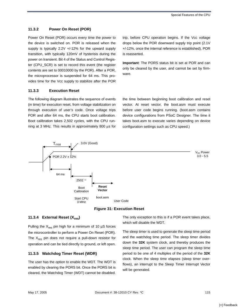
Special Features of the CPU
11.3.2 Power On Reset (POR)
Power On Reset (POR) occurs every time the power to
the device is switched on. POR is released when the
supply is typically 2.2V +/-12% for the upward supply
transition, with typically 120mV of hysterisis during the
power on transient. Bit 4 of the Status and Control Regis-
ter (CPU_SCR) is set to record this event (the register
contents are set to 00010000 by the POR). After a POR,
the microprocessor is suspended for 64 ms. This pro-
vides time for the Vcc supply to stabilize after the POR
trip, before CPU operation begins. If the Vcc voltage
drops below the POR downward supply trip point (2.1V
+/-12%, once the internal reference is established), POR
is reasserted.
Important: The PORS status bit is set at POR and can
only be cleared by the user, and cannot be set by firm-
ware.
11.3.3 Execution Reset
The following diagram illustrates the sequence of events
(in time) for execution reset, from voltage stabilization on
through execution of user’s code. Once voltage trips
POR and after 64 ms, the CPU starts boot calibration.
Boot calibration takes 2,502 cycles, with the CPU run-
ning at 3 MHz. This results in approximately 800 µs for
the time between beginning boot calibration and reset
vector. At reset vector, the boot.asm must execute
before user code begins running. (boot.asm contains
device configurations from PSoC Designer. The time it
takes boot.asm to execute varies depending on device
configuration settings such as CPU speed.)
11.3.4 External Reset (Xres)
Pulling the Xres pin high for a minimum of 10 µS forces
the microcontroller to perform a Power On Reset (POR).
The Xres pin does not require a pull-down resistor for
operation and can be tied directly to ground, or left open.
11.3.5 Watchdog Timer Reset (WDR)
The user has the option to enable the WDT. The WDT is
enabled by clearing the PORS bit. Once the PORS bit is
cleared, the Watchdog Timer (WDT) cannot be disabled.
The only exception to this is if a POR event takes place,
which will disable the WDT.
The sleep timer is used to generate the sleep time period
and the watchdog time period. The sleep timer divides
down the 32K system clock, and thereby produces the
sleep time period. The user can program the sleep time
period to be one of 4 multiples of the period of the 32K
clock. When the sleep time elapses (sleep timer over-
flows), an interrupt to the Sleep Timer Interrupt Vector
will be generated.
Figure 31: Execution Reset
3.0V (Good)
Vcc Power3.0 - 5.5
64 ms
2502 ~
BootCalibration
Start CPU3 MHz
ResetVector
boot.asmUser Code
POR 2.2V ± 12%
TrVdd
May 17, 2005 Document #: 38-12010 CY Rev. *C 115
[+] Feedback

CY8C25122/CY8C26233/CY8C26443/CY8C26643 Device Family Data Sheet
The Watchdog Timer period is automatically set to be 3
counts of the Sleep Timer overflows. This represents
between two and three sleep intervals depending on the
count in the Sleep Timer at the previous WDT clear.
When this timer reaches 3, a WDR is generated.
The user can either clear the WDT, or the WDT and the
Sleep Timer. Whenever the user writes to the Reset
WDT Register (RES_WDT), the WDT will be cleared. If
the data that is written is the hex value 38H, the Sleep
Timer will also be cleared at the same time.
This timer chain is also used to time the startup for the
external 32 kHz crystal oscillator. When selecting the
external 32 kHz oscillator, a value of 1 second must be
selected as the sleep interval. When the sleep interrupt
occurs, the 32 kHz oscillator source will switch from
internal to the crystal. The device does not have to be
put into sleep for this event to occur. Note that if too short
of a sleep interval is given, the crystal oscillator will not
be stable prior to switch over and the results will be
unpredictable.
Reset WDT Register (RES_WDT, Address = Bank 0, E3h)
11.4 Sleep States
There are three sleep states that can be used to lower
the overall power consumption on the device. The three
states are CPU Sleep, Analog Sleep, and Full Sleep.
The CPU can only be put to sleep by the firmware. This
is accomplished by setting the Sleep Bit in the Status
and Control Register (CPU_SCR). This stops the CPU
from executing instructions, and the CPU will remain
asleep until an interrupt comes pending, or there is a
reset event (either a Power On Reset, or a Watchdog
Timer Reset). While in the CPU Sleep state, all clocking
signals derived from the Internal Main Oscillator are
inactivated, including the 48M, 24M, 24V1, and 24V2
system clocking signals. The Internal Low Speed Oscilla-
tor will continue to operate during the CPU Sleep state.
The function of any analog or digital PSoC block that is
clocked from these system-clocking signals will stop dur-
ing the CPU Sleep state.
The user can also put all the analog PSoC block circuits
to sleep. This is accomplished by resetting the Analog
Array Power Control bits in the Analog Reference Con-
trol Register (ARF_CR), which overrides the individual
enable bits within each analog PSoC block. Setting the
Analog Array Power Control bits will restore the function
to those analog PSoC blocks that were previously in use.
The user should take into account the required settling
time after an analog PSoC block is enabled before it will
provide the maximum precision.
For greatest power savings, the user should put the
device in the Full Sleep state. This is accomplished by
first transitioning to the Analog Sleep state, and then set-
ting the Sleep Bit in the CPU_SCR Register to the Full
Sleep state. The CPU will be stopped at this point, and
either an interrupt or reset event is required to transition
back to the Analog Sleep state.
The Voltage Reference and Supply Voltage Monitor drop
into (fully functional) power-reduced states. All interrupts
remain active. The Internal Low Speed Oscillator
remains running (it will however drop into a less accu-
rate, low-power state). If enabled, the External Crystal
Oscillator will continue running throughout sleep (the
Internal Low Speed Oscillator is disabled if the External
Crystal Oscillator is selected). Only the occurrence of an
Table 95: Reset WDT Register
Bit # 7 6 5 4 3 2 1 0
POR 0 0 0 0 0 0 0 0
Read/Write W W W W W W W W
Bit Name Data [7] Data [6] Data [5] Data [4] Data [3] Data [2] Data [1] Data [0]
Bit [7:0]: Data [7:0] Any write to this register will clear Watchdog Timer, a write of 38h will also clear the Sleep Timer
116 Document #: 38-12010 CY Rev. *C May 17, 2005
[+] Feedback

Special Features of the CPU
interrupt will wake the part from sleep. The Stop bit in the
Status and Control Register (CPU_SCR) must be
cleared for a part to resume out of sleep.
Any digital PSoC block that is clocked by a System Clock
other than the 32K system-clocking signal or external
pins will be stopped, as these clocks do not run in sleep
mode.
The Internal Main Oscillator restarts immediately on exit-
ing either the Full Sleep or CPU Sleep modes. Analog
functions must be re-enabled by firmware. If the External
Crystal Oscillator is used and the internal PLL is
enabled, the PLL will take many cycles to change from
its initial 2.5% accuracy to track that of the External Crys-
tal Oscillator. If the PLL is enabled, there will be a 30µs
(one full 32K cycle) delay hold-off time for the CPU to let
the VCO and PLL stabilize. If the PLL is not enabled, the
hold-off time is one half of the 32K cycle. For further
details on PLL, see 7.0.
The Sleep interrupt allows the microcontroller to wake up
periodically and poll system components while maintain-
ing very low average power consumption. The sleep
interrupt may also be used to provide periodic interrupts
during non-sleep modes.
In System Sleep State, GPIO Pins P2[4] and P2[6]
should be held to a logic low or a false Low Voltage
Detect interrupt may be triggered. The cause is in the
System Sleep State, the internal Bandgap reference
generator is turned off and the reference voltage is main-
tained on a capacitor.
The circumstances are that during sleep, the reference
voltage on the capacitor is refreshed periodically at the
sleep system duty cycle. Between refresh cycles, this
voltage may leak slightly to either the positive supply or
ground. If pins P2[4] or P2[6] are in a high state, the leak-
age to the positive supply is accelerated (especially at
high temperature). Since the reference voltage is com-
pared to the supply to detect a low voltage condition, this
accelerated leakage to the positive supply voltage will
cause that voltage to appear lower than it actually is,
leading to the generation of a false Low Voltage Detect
interrupt.
Figure 32: Three Sleep States
RunAnalogSleep
CPU Running
CPU not Running
Full SleepCPU Sleep
May 17, 2005 Document #: 38-12010 CY Rev. *C 117
[+] Feedback
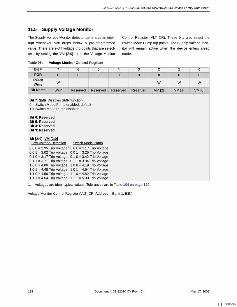
CY8C25122/CY8C26233/CY8C26443/CY8C26643 Device Family Data Sheet
11.5 Supply Voltage Monitor
The Supply Voltage Monitor detector generates an inter-
rupt whenever Vcc drops below a pre-programmed
value. There are eight voltage trip points that are select-
able by setting the VM [2:0] bit in the Voltage Monitor
Control Register (VLT_CR). These bits also select the
Switch Mode Pump trip points. The Supply Voltage Mon-
itor will remain active when the device enters sleep
mode.
Voltage Monitor Control Register (VLT_CR, Address = Bank 1, E3h)
Table 96: Voltage Monitor Control Register
Bit # 7 6 5 4 3 2 1 0
POR 0 0 0 0 0 0 0 0Read/Write W -- -- -- -- W W W
Bit Name SMP Reserved Reserved Reserved Reserved VM [2] VM [1] VM [0]
Bit 7: SMP Disables SMP function0 = Switch Mode Pump enabled, default1 = Switch Mode Pump disabled
Bit 6: ReservedBit 5: ReservedBit 4: ReservedBit 3: Reserved
Bit [2:0]: VM [2:0] Low Voltage Detection Switch Mode Pump
0 0 0 = 2.95 Trip Voltage1 0 0 0 = 3.17 Trip Voltage0 0 1 = 3.02 Trip Voltage 0 0 1 = 3.25 Trip Voltage0 1 0 = 3.17 Trip Voltage 0 1 0 = 3.42 Trip Voltage0 1 1 = 3.71 Trip Voltage 0 1 1 = 3.94 Trip Voltage1 0 0 = 4.00 Trip Voltage 1 0 0 = 4.19 Trip Voltage1 0 1 = 4.48 Trip Voltage 1 0 1 = 4.64 Trip Voltage1 1 0 = 4.56 Trip Voltage 1 1 0 = 4.82 Trip Voltage1 1 1 = 4.64 Trip Voltage 1 1 1 = 5.00 Trip Voltage
1. Voltages are ideal typical values. Tolerances are in Table 104 on page 129.
118 Document #: 38-12010 CY Rev. *C May 17, 2005
[+] Feedback
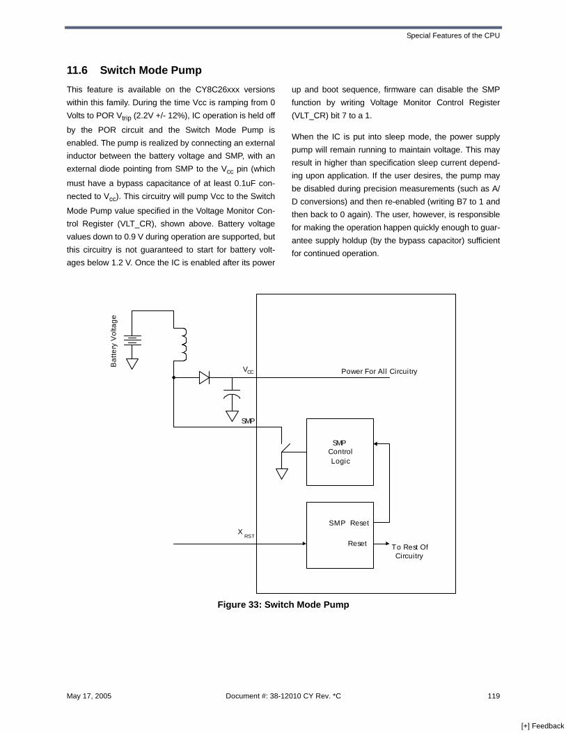
Special Features of the CPU
11.6 Switch Mode Pump
This feature is available on the CY8C26xxx versions
within this family. During the time Vcc is ramping from 0
Volts to POR Vtrip (2.2V +/- 12%), IC operation is held off
by the POR circuit and the Switch Mode Pump is
enabled. The pump is realized by connecting an external
inductor between the battery voltage and SMP, with an
external diode pointing from SMP to the Vcc pin (which
must have a bypass capacitance of at least 0.1uF con-
nected to Vcc). This circuitry will pump Vcc to the Switch
Mode Pump value specified in the Voltage Monitor Con-
trol Register (VLT_CR), shown above. Battery voltage
values down to 0.9 V during operation are supported, but
this circuitry is not guaranteed to start for battery volt-
ages below 1.2 V. Once the IC is enabled after its power
up and boot sequence, firmware can disable the SMP
function by writing Voltage Monitor Control Register
(VLT_CR) bit 7 to a 1.
When the IC is put into sleep mode, the power supply
pump will remain running to maintain voltage. This may
result in higher than specification sleep current depend-
ing upon application. If the user desires, the pump may
be disabled during precision measurements (such as A/
D conversions) and then re-enabled (writing B7 to 1 and
then back to 0 again). The user, however, is responsible
for making the operation happen quickly enough to guar-
antee supply holdup (by the bypass capacitor) sufficient
for continued operation.
Figure 33: Switch Mode Pump
To Rest OfCircuitry
XRST
SMP
SMPControlLogic
SMP Reset
Reset
Power For All CircuitryVCC
Ba
tte
ry V
olta
ge
May 17, 2005 Document #: 38-12010 CY Rev. *C 119
[+] Feedback

CY8C25122/CY8C26233/CY8C26443/CY8C26643 Device Family Data Sheet
11.7 Internal Voltage Reference
An internal bandgap voltage reference source is pro-
vided on-chip. This reference is used for the Supply Volt-
age Monitor, and can also be accessed by the user as a
reference voltage for analog operations. There is a
Bandgap Oscillator Trim Register (BDG_TR) used to cal-
ibrate this reference into specified tolerance. Factory-
programmed trim values are available for 5.0V and 3.3V
operation. The 5.0V value is loaded in the BDG_TR reg-
ister upon reset. This register must be adjusted when
operating voltage outside the range for which factory cal-
ibration was set. Changing the factory-programmed trim
value is done using the Table Read Supervisor Call rou-
tine, and is documented in 11.8.
Bandgap Trim Register (BDG_TR, Address = Bank 1, EAh)
11.8 Supervisor ROM/System Supervisor Call Instruction
The parts in this family have a Supervisor ROM to man-
age the programming, erasure, and protection of the on-
chip Flash user program space. The Supervisor ROM
also gives the user the capability to read the internal
product ID, access factory trim values, as well as calcu-
late checksums on blocks of the Flash memory space.
The System Supervisor Call instruction (SSC, opcode/
byte 00h) provides the method for the user to access the
pre-existing routines in the Supervisor ROM to imple-
ment these functions. This instruction sets the Flags
Register (CPU_F) bit 3 to 1 and performs an interrupt to
address 0000 into the Supervisory ROM. The flag and
old PC are pushed onto the Stack. The fact that the flag
pushed has F[3] = 1 is irrelevant as the RETI instruction
always clears F[3]. The Supervisory code at 0000 does a
JACC table lookup based on the Accumulator value,
which is effectively another level of instruction encoding.
This service table implements the vectors to the various
supervisory functions. The user must set several param-
eters when utilizing these functions. The parameters are
written to 5 bytes of an 8-byte block near the top of RAM
memory space.
Access to these functions must be through the Flash
APIs provided in PSoC Designer and described in Appli-
cation Note AN2015.
The following table documents each function, as well as
the required parameter values:
Table 97: Bandgap Trim Register
Bit # 7 6 5 4 3 2 1 0
POR FS1 FS1 FS1 FS1 FS1 FS1 FS1 FS1
Read/Write W W W W W W W W
Bit Name FMRD BGT[2] BGT[1] BGT[0] BGO[3] BGO[2] BGO[1] BGO[0]
Bit 7: FMRD0 = Enable voltage divider between BG and Flash (User must not use other than this setting)1 = Disable voltage divider between BG and Flash (Test purposes only)
Bit [6:4]: BGT [2:0] Provides Temperature Curve compensation Bit [3:0]: BGO [3:0] Provides +/- 5% Offset Trim to center Vbg to 1.30V
1. FS = Factory set trim value
120 Document #: 38-12010 CY Rev. *C May 17, 2005
[+] Feedback

Special Features of the CPU
Notes:
NA: Not applicable
*: Indeterminate
Blk ID: Number of 64-byte block within FLASH memory space
Clock: CPU system clocking signal value
Pointer: Address of first byte of 64-byte block within SRAM memory space
TV: Table value
Table 98: CY8C25122, CY8C26233, CY8C26443, CY8C26643 (256 Bytes of SRAM)
Operation Function
Accu
mu
lator
Input SRAM Data Output SRAM Data
F8h F9h FAh FBh FCh FDh FEh FFh F8h F9h FAh FBh FCh FDh FEh FFh
Reset1
1. This is a software-only reset.
Calibrates then sets PC and SP values to 0
00 NA NA NA NA NA NA NA NA * * * * * * * *
Read Block
Move block of 64 bytes of FLASH data into SRAM
01 3Ah SP+3
Blk ID Pointer NA 0 0 0 0 0 * * * * * *
Write Block2
2. This operation should only be invoked by calling a function in the FlashBlock library. Device specifications are no longer guaranteed if this function is directly called by the user’s code.
Program block of FLASH with data from SRAM
02 3Ah SP+3
Blk ID
Pointer Clock 0 0 0 0 0 * * * * * *
Erase Block Erase block of FLASH
03 3Ah SP+3
Blk ID
NA Clock 0 0 0 0 0 * * * * * *
Protect Block3
3. This function can only be invoked by the device programmer, not by user’s code.
Set memory protection bits4
4. The address is hard coded by algorithm.
04 3Ah SP+3
NA NA Clock 0 0 0 0 0 * * * * * *
Erase All3Erase all FLASH data
05 3Ah SP+3
NA NA Clock 0 0 0 0 0 * * * * * *
Table Read Read device type code
06 3Ah SP+3
Tbl ID
NA NA NA NA NA TV(0)
TV(1)
TV(2)
TV(3)
TV(4)
TV(5)
TV(6)
TV(7)
Checksum
Calculate FLASH checksum for data range speci-fied
07 3AhSP+3
Blk Counter
NA NA 0 0 0CSH CSL * * * * * *
Calibrate5
5. User-writeable registers include Main Oscillator Trim (IMO_TR), Internal Low Speed Oscillator Trim (ILO_TR), and Bandgap Trim (BDG_TR).
Sets user-writable reg-isters to default
08 3AhSP+3 NA NA NA 0 0 * * * * * *
May 17, 2005 Document #: 38-12010 CY Rev. *C 121
[+] Feedback

CY8C25122/CY8C26233/CY8C26443/CY8C26643 Device Family Data Sheet
11.8.1 Additional Function for Table Read Supervisory Call
The Table Read supervisory operation will return the Ver-
sion ID in the Accumulator. The value in the Accumulator
is divided into a high and low nibble, indicating major and
minor revisions, respectively. Note: The value in the X
register is modified during the Table Read Supervisory
Call, and must be saved and restored if needed after the
call completes.
A[7:4]: Major silicon revisions.
A[3:0]: Minor silicon revisions.
11.9 Flash Program Memory Protection
The user has the option to define the access to the Flash
memory. A flexible system allows the user to select one
of four protection modes for each 64-byte block within
the Flash, based on the particular application. The pro-
tection mechanism is implemented by a device program-
mer using the System Supervisor Call. When this
command is executed, two bits within the data pro-
grammed into the Flash will select the protection mode.
It is not intended that the protection byte will be modified
by the user’s code. The following table lists the available
protection options:
Note: Mode 10 is the default.
11.10 Programming Requirements and Step Descriptions
The pins in the following table are critical for the pro-
grammer:
Table 99: Table Read for Supervisory Call Functions
Table ID
Function TV(0) TV(1) TV(2) TV(3) TV(4) TV(5) TV(6) TV(7)
001
1. Determines silicon revision values in Accumulator and X registers.
Produc-tion Sili-con ID
Silicon ID 1
Silicon ID 0
Reserved Reserved Reserved Reserved Reserved Reserved
01
Provides trim value for Inter-nal Main Oscillator and Inter-nal Volt-age Refer-ence
Internal Voltage Refer-ence trim value for 3.3V
Internal Main Oscillator trim value for 3.3V
Reserved Reserved
Internal Voltage Refer-ence trim value for 5.0V
Internal Main Oscilla-tor trim value for 5.0V
Reserved Reserved
Table 100: Flash Program Memory Protection
Mode Bits
Mode NameExternal
ReadExternal
WriteInternal
Write
00 Unprotected Enabled Enabled Enabled
01 Factory Upgrade
Disabled Enabled Enabled
10 Field Upgrade Disabled Disabled Enabled
11 Full Protection Disabled Disabled Disabled
Table 101: Programmer Requirements
Pin Name
FunctionProgrammer HW Pin
Requirements
SDATA Serial Data In/OutDrive TTL Levels, Read TTL, High Z
SCLK Serial ClockDrive TTL levEl Clock Signal
Vss
Power Supply Ground Connec-tion
Low Resistance Ground Connection
VccPower Supply Positive Voltage
0V, 3.0V, 5V, & 5.4V. 0.1V Accuracy. 20mA Current Capability
122 Document #: 38-12010 CY Rev. *C May 17, 2005
[+] Feedback

Special Features of the CPU
11.10.1 Data File Read
The user’s data file should be read into the programmer.
The checksum should be calculated by the programmer
for each record and compared to the record checksum
stored in the file for each record. If there is an error, a
message should be sent to the user explaining that the
file has a checksum error and the programming should
not be allowed to continue.
11.10.2 Programmer Flow
The following sequence (with descriptions) is the main
flow used to program the devices: (Note that failure at
any step will result in termination of the flow and an error
message to the device programmer’s operator.)
11.10.2.1 Verify Silicon ID
The silicon ID is read and verified against the expected
value. If it is not the expected value, then the device is
failed and an error message is sent to the device pro-
grammer’s operator.
This test will detect a bad connection to the programmer
or an incorrect device selection on the programmer.
The silicon ID test is required to be first in the flow and
cannot be bypassed. The sequence is as follows:
Set Vcc=0VSet SDATA=HighZSet SCLK=VILPSet Vcc=VccpStart the programmer’s SCLK driver “free running”WAIT-AND-POLL ID-SETUPWAIT-AND-POLLREAD-ID-WORD
Notes: See “DC Specifications“ table in section 13 for
value of Vccp and VILP. See “AC Specifications” table in
section 13 for value of frequency for the SCLK driver
(Fsclk).
11.10.2.2 Erase
The Flash memory is erased. This is accomplished by
the following sequence:
SET-CLK-FREQ(num_MHz_times_5)
Erase AllWAIT-AND-POLL
11.10.2.3 Program
The Flash is programmed with the contents of the user’s
programming file. This is accomplished by the following
sequence:
For num_block = 0 to max_data_blockFor address =0 to 63WRITE-BYTE(address,data):End for address loopSET-CLK-FREQ(num_MHz_times_5)SET-BLOCK-NUM(num_block)PROGRAM-BLOCKWAIT-AND-POLLEnd for num_block loop
11.10.2.4 Verify (at Low Vcc and High Vcc)
The device data is read out to compare to the data in the
user’s programming file. This is accomplished by the fol-
lowing sequence:
For num_block = 0 to max_data_blockSET-BLOCK-NUM (num_block)VERIFY-SETUPWait & POLL the SDATA for a high to low transitionFor address =0 to max_byte_per_blockREAD-BYTE(address,data)End for address loopEnd for num_block loop
Note: This should be done 2 times; once at Vcc=Vcclv
and once at Vcc=Vcchv.
11.10.2.5 Set Security
The security operation protects certain blocks from being
read or changed. This is done at the end of the flow so
that the security does not interfere with the verify step.
Security is set with the following sequence:
For address =0 to 63WRITE-SECURITY-BYTE(address,data):End for address loopSET-CLK-FREQ(num_MHz_times_5)SECUREWAIT-AND-POLL
Note: This sequence is done at Vcc=Vccp.
May 17, 2005 Document #: 38-12010 CY Rev. *C 123
[+] Feedback

CY8C25122/CY8C26233/CY8C26443/CY8C26643 Device Family Data Sheet
11.10.2.6 Device Checksum (at Low Vcc and High Vcc)
The device checksum is retrieved from the device and
compared to the “Device Checksum” from the user’s file
(Note that this is NOT the same thing as the “Record
Checksum.”) The checksum is retrieved from the device
with the following sequence:
CHECKSUM-SETUP(max_data_block)WAIT-AND-POLLREAD-CHECKSUM(data)
Note: This should be done 2 times; once at Vcc=Vcchv
and once at Vcc=Vcclv.
11.10.2.7 Power Down
The last step is to power down the device. This is
accomplished by the following sequence:
Set SDATA=HighZ (float pin P1[0])Set SCLK=0V (Vin on pin P1[1]=Vilp)Set Vcc = 0V
11.11 Programming Wave Forms
Notes:
11.12 Programming File Format
The programming file is created by PSoC Designer, the
Cypress MicroSystems development tool. This tool gen-
erates the programming file in an Intel Hex format.
The programmer should assume the data is 30h/HALT if
it is not specified in the user’s data file.
Figure 34: Programming Wave Forms
Vcc
SDATA
SCLK
OUT OUT IN IN
Tssclk Thsclk
1 Vcc is only turned off (0V) at the very beginning and the very end of the flow - not within the programming flow.
2When the programmer puts the driver on SDATA in a High Z (floating) state, the SDATA pin will float to a low due to an internal device pull down circuit.
3
SCLK is set to VILP during the power up and power down; at other times the SCLK is “free running.” The fre-quency of the hardware’s SCLK signal must be known by the software because the value (entered in the num-ber of MegaHertz multiplied by the number 5) must be passed into the device with the SET-CLK-FREQ() mnemonic.
124 Document #: 38-12010 CY Rev. *C May 17, 2005
[+] Feedback
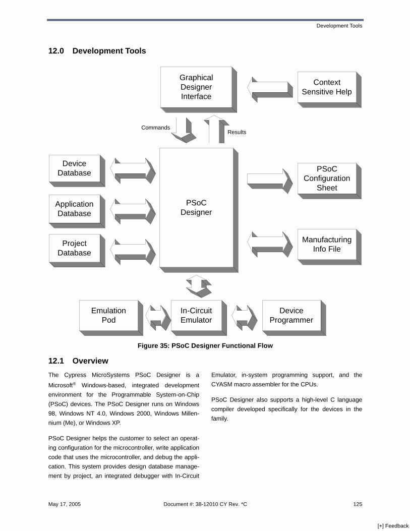
Development Tools
12.0 Development Tools
12.1 Overview
The Cypress MicroSystems PSoC Designer is a
Microsoft® Windows-based, integrated development
environment for the Programmable System-on-Chip
(PSoC) devices. The PSoC Designer runs on Windows
98, Windows NT 4.0, Windows 2000, Windows Millen-
nium (Me), or Windows XP.
PSoC Designer helps the customer to select an operat-
ing configuration for the microcontroller, write application
code that uses the microcontroller, and debug the appli-
cation. This system provides design database manage-
ment by project, an integrated debugger with In-Circuit
Emulator, in-system programming support, and the
CYASM macro assembler for the CPUs.
PSoC Designer also supports a high-level C language
compiler developed specifically for the devices in the
family.
Figure 35: PSoC Designer Functional Flow
DeviceDatabase
PSoCDesigner
ApplicationDatabase
ProjectDatabase
In-CircuitEmulator
DeviceProgrammer
ManufacturingInfo File
PSoCConfiguration
Sheet
GraphicalDesignerInterface
CommandsResults
ContextSensitive Help
EmulationPod
May 17, 2005 Document #: 38-12010 CY Rev. *C 125
[+] Feedback
CY8C25122/CY8C26233/CY8C26443/CY8C26643 Device Family Data Sheet
12.2 Integrated Development Environment Subsystems
12.2.1 Online Help System
The online help system displays online, context-sensitive
help for the user. Designed for procedural and quick ref-
erence, each functional subsystem has its own context-
sensitive help. This system also provides tutorials and
links to FAQs and an Online Support Forum to aid the
designer in getting started.
12.2.2 Device Editor
PSoC Designer has several main functions. The Device
Editor subsystem lets the user select different onboard
analog and digital component configurations for the
PSoC blocks. PSoC Designer sets up power-on initial-
ization tables for selected PSoC block configurations and
creates source code for an application framework. The
framework contains software to operate the selected
components and, if the project uses more than one oper-
ating configuration, contains routines to switch between
different sets of PSoC block configurations at runtime.
PSoC Designer can print out a configuration sheet for
given project configuration for use during application pro-
gramming in conjunction with the Device Data Sheet.
Once the framework is generated, the user can add
application-specific code to flesh out the framework. It’s
also possible to change the selected components and
regenerate the framework.
12.2.3 Assembler
The included CYASM macro assembler supports the
M8C microcontroller instruction set and generates a load
file ready for device programming or system debugging
using the ICE hardware.
12.2.4 C Language Software Development
A C language compiler supports Cypress MicroSystems’
PSoC family devices. Even if you have never worked in
the C language before, the product quickly allows you to
create complete C programs for the PSoC family
devices.
The embedded, optimizing C compiler provides all the
features of C tailored to the PSoC architecture. It
includes a built-in macro assembler allowing assembly
code to be merged seamlessly with C code. The link
libraries automatically use absolute addressing or can be
compiled in relative mode, and linked with other software
modules to get absolute addressing.
The compiler comes complete with embedded libraries
providing port and bus operations, standard keypad and
display support, and extended math functionality.
12.2.5 Debugger
The PSoC Designer Debugger subsystem provides
hardware in-circuit emulation, allowing the designer to
test the program in a physical system while providing an
internal view of the PSoC device. Debugger commands
allow the designer to read and write program and data
memory, read and write I/O registers, read and write
CPU registers, set and clear breakpoints, and provide
program run, halt, and step control. The debugger also
allows the designer to create a trace buffer of registers
and memory locations of interest.
12.3 Hardware Tools
12.3.1 In-Circuit Emulator
A low cost, high functionality ICE is available for devel-
opment support. This hardware has the capability to pro-
gram single devices.
126 Document #: 38-12010 CY Rev. *C May 17, 2005
[+] Feedback

DC and AC Characteristics
13.0 DC and AC CharacteristicsSpecifications are valid for -40 oC </= TA </= 85 oC and TJ </= 100 oC as specified, except where noted. Specifications
for devices running at 24 MHz are valid at -40 oC </= TA </= 70oC and TJ </= 82 oC.
13.1 Absolute Maximum Ratings
Figure 36: CY8C25xxx/CY8C26xxx Voltage Frequency Graph
Table 102: Absolute Maximum Ratings
Symbol Absolute Maximum Ratings Minimum Typical Maximum Unit
Storage Temperature -65 - +100 1
1. Higher storage temperatures will reduce data retention time.
oC
Ambient Temperature with Power Applied -40 - +85 oC
Supply Voltage on Vcc Relative to Vss -0.5 - +6.0 V
DC Input Voltage -0.5 - Vcc+0.5 V
DC Voltage Applied to Tri-state Vss-0.5 - Vcc+0.5 V
Maximum Current into any Port Pin -25 - +50 mA
Maximum Current into any Port Pin Config-ured as Analog Driver
-50 - +50 mA
Junction Temperature up to 12 MHz - - 1002 oC
Junction Temperature at 24 MHz - - 82 oC
Static Discharge Voltage 2000 - - V
Latch-up Current 200 - - mA
5.25
4.75
3.00
93 kHz 12 MHz 24 MHzCPU Frequency
Vo
ltage
May 17, 2005 Document #: 38-12010 CY Rev. *C 127
[+] Feedback

CY8C25122/CY8C26233/CY8C26443/CY8C26643 Device Family Data Sheet
2. The temperature rise from junction to ambient is package specific. (See Table 122 on page 149 for thermal imped-ances of available packages.) User must limit power consumption to comply with this requirement.
Table 103: Temperature Specifications
Symbol Temperature Specifications Minimum Typical Maximum Unit
TA Ambient Temperature -40 24 +85 oC
TJ Junction Temperature -40 100 oC
128 Document #: 38-12010 CY Rev. *C May 17, 2005
[+] Feedback

DC and AC Characteristics
13.2 DC Characteristics
Table 104: DC Operating Specifications
Symbol DC Operating Specifications Minimum Typical Maximum Unit
Vcc Supply Voltage 3.00 - 5.25 V
Icc Supply Current - 5 81
1. Conditions are 5.0V, 25 oC, 3 MHz.
mA
Isb Sleep (Mode) Current - - 52
2. Without Crystal Oscillator, Vcc = 3.3 V, TA <= 85 oC.
µA
Isbxtl Sleep (Mode) Current with Crystal Oscillator - 3 53
3. Conditions are 3.0V <= Vcc <= 3.6V, -40 oC <= TA <= 85 oC. Correct operation assumes a properly loaded, 1 uW maximum drive level, 32.768 kHz crystal.
µA
Vref Reference Voltage (Bandgap) 1.275 1.3 1.3254
4. Trimmed for appropriate Vcc.
V
Vil Input Low Voltage - - 0.8 V
Vih Input High Voltage 2.2 - - V
Vh Hysterisis Voltage - 60 - mV
Vol Output Low Voltage - - Vss+0.755
5. Isink = 25 mA, Vcc = 4.5 V (maximum of 8 IO sinking, 4 on each side of the IC).
V
Voh Output High Voltage Vcc-1.06
6. Isource =10 mA, Vcc = 4.5 V (maximum of 8 IO sourcing, 4 on each side of the IC).
- - V
Rpu Pull Up Resistor Value 4000 5600 8000 Ω
Rpd Pull Down Resistor Value 4000 5600 8000 Ω
Iil Input Leakage (Absolute Value) - 0.1 5 µA
Cin Capacitive Load on Pins as Input 0.5 1.7 107
7. Package dependent.
pF
Cout Capacitive Load on Pins as Output 0.5 1.7 107 pF
VLVD LVD and SMP Tolerance8
8. Ideal values are +/- 5% absolute tolerance and +/- 1% tolerance relative to each other (for adjacent levels).
0.95 x Ideal8 Ideal 1.05 x Ideal8 V
May 17, 2005 Document #: 38-12010 CY Rev. *C 129
[+] Feedback
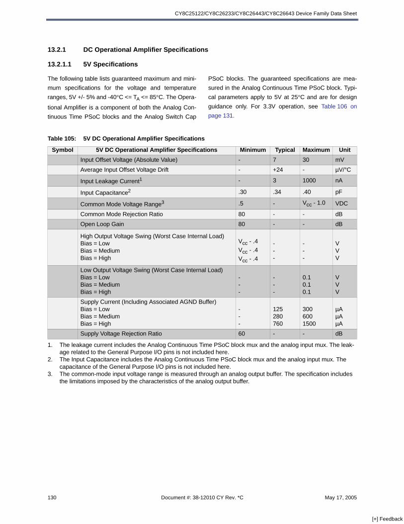
CY8C25122/CY8C26233/CY8C26443/CY8C26643 Device Family Data Sheet
13.2.1 DC Operational Amplifier Specifications
13.2.1.1 5V Specifications
The following table lists guaranteed maximum and mini-
mum specifications for the voltage and temperature
ranges, 5V +/- 5% and -40°C <= TA <= 85°C. The Opera-
tional Amplifier is a component of both the Analog Con-
tinuous Time PSoC blocks and the Analog Switch Cap
PSoC blocks. The guaranteed specifications are mea-
sured in the Analog Continuous Time PSoC block. Typi-
cal parameters apply to 5V at 25°C and are for design
guidance only. For 3.3V operation, see Table 106 on
page 131.
Table 105: 5V DC Operational Amplifier Specifications
Symbol 5V DC Operational Amplifier Specifications Minimum Typical Maximum Unit
Input Offset Voltage (Absolute Value) - 7 30 mV
Average Input Offset Voltage Drift - +24 - µV/°C
Input Leakage Current1
1. The leakage current includes the Analog Continuous Time PSoC block mux and the analog input mux. The leak-age related to the General Purpose I/O pins is not included here.
- 3 1000 nA
Input Capacitance2
2. The Input Capacitance includes the Analog Continuous Time PSoC block mux and the analog input mux. The capacitance of the General Purpose I/O pins is not included here.
.30 .34 .40 pF
Common Mode Voltage Range3
3. The common-mode input voltage range is measured through an analog output buffer. The specification includes the limitations imposed by the characteristics of the analog output buffer.
.5 - Vcc - 1.0 VDC
Common Mode Rejection Ratio 80 - - dB
Open Loop Gain 80 - - dB
High Output Voltage Swing (Worst Case Internal Load)Bias = LowBias = MediumBias = High
Vcc - .4
Vcc - .4
Vcc - .4
---
---
VVV
Low Output Voltage Swing (Worst Case Internal Load)Bias = LowBias = MediumBias = High
---
---
0.10.10.1
VVV
Supply Current (Including Associated AGND Buffer)Bias = LowBias = MediumBias = High
---
125280760
3006001500
µAµAµA
Supply Voltage Rejection Ratio 60 - - dB
130 Document #: 38-12010 CY Rev. *C May 17, 2005
[+] Feedback

DC and AC Characteristics
13.2.1.2 3.3V Specifications
The following table lists guaranteed maximum and mini-
mum specifications for the voltage and temperature
ranges, 3.3V +/- 10% and -40°C <= TA <= 85°C. The
Operational Amplifier is a component of both the Analog
Continuous Time PSoC blocks and the Analog Switch
Cap PSoC blocks. The guaranteed specifications are
measured in the Analog Continuous Time PSoC block.
Typical parameters apply to 5V at 25°C and are for
design guidance only. For 5V operation, see Table 105
on page 130.
Table 106: 3.3V DC Operational Amplifier Specifications
Symbol 3.3V DC Operational Amplifier Specifications Minimum Typical Maximum Unit
Input Offset Voltage (Absolute Value) - 7 30 mV
Average Input Offset Voltage Drift - +24 - µV/°C
Input Leakage Current1
1. The leakage current includes the Analog Continuous Time PSoC block mux and the analog input mux. The leak-age related to the General Purpose I/O pins is not included here.
- 2 700 nA
Input Capacitance2
2. The Input Capacitance includes the Analog Continuous Time PSoC block mux and the analog input mux. The capacitance of the General Purpose I/O pins is not included here.
.32 .36 .42 pF
Common Mode Voltage Range3
3. The common-mode input voltage range is measured through an analog output buffer. The specification includes the limitations imposed by the characteristics of the analog output buffer
.5 - Vcc - 1.0 VDC
Common Mode Rejection Ratio 80 - - dB
Open Loop Gain 80 - - dB
High Output Voltage Swing (Worst Case Internal Load)Bias = LowBias = MediumBias = High
Vcc - .4
Vcc - .4
Vcc - .4
---
---
VVV
Low Output Voltage Swing (Worst Case Internal Load)Bias = LowBias = MediumBias = High
---
---
0.10.10.1
VVV
Supply Current (Including Associated AGND Buffer)Bias = LowBias = MediumBias = High
---
80112320
200300800
µAµAµA
Supply Voltage Rejection Ratio 60 - - dB
May 17, 2005 Document #: 38-12010 CY Rev. *C 131
[+] Feedback
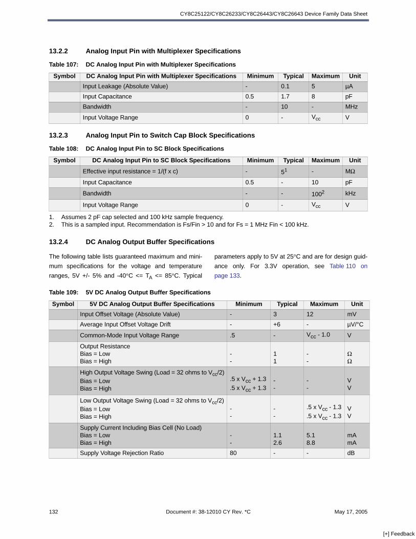
CY8C25122/CY8C26233/CY8C26443/CY8C26643 Device Family Data Sheet
13.2.2 Analog Input Pin with Multiplexer Specifications
13.2.3 Analog Input Pin to Switch Cap Block Specifications
13.2.4 DC Analog Output Buffer Specifications
The following table lists guaranteed maximum and mini-
mum specifications for the voltage and temperature
ranges, 5V +/- 5% and -40°C <= TA <= 85°C. Typical
parameters apply to 5V at 25°C and are for design guid-
ance only. For 3.3V operation, see Table 110 on
page 133.
Table 107: DC Analog Input Pin with Multiplexer Specifications
Symbol DC Analog Input Pin with Multiplexer Specifications Minimum Typical Maximum Unit
Input Leakage (Absolute Value) - 0.1 5 µA
Input Capacitance 0.5 1.7 8 pF
Bandwidth - 10 - MHz
Input Voltage Range 0 - Vcc V
Table 108: DC Analog Input Pin to SC Block Specifications
Symbol DC Analog Input Pin to SC Block Specifications Minimum Typical Maximum Unit
Effective input resistance = 1/(f x c) - 51
1. Assumes 2 pF cap selected and 100 kHz sample frequency.
- MΩ
Input Capacitance 0.5 - 10 pF
Bandwidth - - 1002
2. This is a sampled input. Recommendation is Fs/Fin > 10 and for Fs = 1 MHz Fin < 100 kHz.
kHz
Input Voltage Range 0 - Vcc V
Table 109: 5V DC Analog Output Buffer Specifications
Symbol 5V DC Analog Output Buffer Specifications Minimum Typical Maximum Unit
Input Offset Voltage (Absolute Value) - 3 12 mV
Average Input Offset Voltage Drift - +6 - µV/°C
Common-Mode Input Voltage Range .5 - Vcc - 1.0 V
Output ResistanceBias = LowBias = High
--
11
--
ΩΩ
High Output Voltage Swing (Load = 32 ohms to Vcc/2)Bias = LowBias = High
.5 x Vcc + 1.3
.5 x Vcc + 1.3--
--
VV
Low Output Voltage Swing (Load = 32 ohms to Vcc/2)Bias = LowBias = High
--
--
.5 x Vcc - 1.3
.5 x Vcc - 1.3VV
Supply Current Including Bias Cell (No Load)Bias = LowBias = High
--
1.12.6
5.18.8
mAmA
Supply Voltage Rejection Ratio 80 - - dB
132 Document #: 38-12010 CY Rev. *C May 17, 2005
[+] Feedback

DC and AC Characteristics
The following table lists guaranteed maximum and mini-
mum specifications for the voltage and temperature
ranges, 3.3V +/- 10% and -40°C <= TA <= 85°C. Typical
parameters apply to 5V at 25°C and are for design guid-
ance only. For 5V operation, see Table 109 on page 132.
Table 110: 3.3V DC Analog Output Buffer Specifications
Symbol 3.3V DC Analog Output Buffer Specifications Minimum Typical Maximum Unit
Input Offset Voltage (Absolute Value) - 3 12 mV
Average Input Offset Voltage Drift - +6 - µV/°C
Common-Mode Input Voltage Range .5 - Vcc - 1.0 V
Output ResistanceBias = LowBias = High
--
11
--
ΩΩ
High Output Voltage Swing (Load = 32 ohms to Vcc/2)Bias = LowBias = High
.5 x Vcc + 1.3
.5 x Vcc + 1.3--
--
VV
Low Output Voltage Swing (Load = 32 ohms to Vcc/2)Bias = LowBias = High
--
--
.5 x Vcc - 1.3
.5 x Vcc - 1.3VV
Supply Current Including Bias Cell (No Load)Bias = LowBias = High
--
0.82.0
2.04.3
mAmA
Supply Voltage Rejection Ratio 80 - - dB
May 17, 2005 Document #: 38-12010 CY Rev. *C 133
[+] Feedback
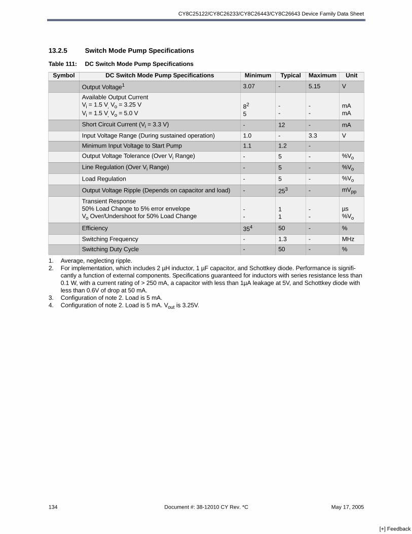
CY8C25122/CY8C26233/CY8C26443/CY8C26643 Device Family Data Sheet
13.2.5 Switch Mode Pump Specifications
Table 111: DC Switch Mode Pump Specifications
Symbol DC Switch Mode Pump Specifications Minimum Typical Maximum Unit
Output Voltage1
1. Average, neglecting ripple.
3.07 - 5.15 V
Available Output CurrentVi = 1.5 V, Vo = 3.25 VVi = 1.5 V, Vo = 5.0 V
82
5
2. For implementation, which includes 2 µH inductor, 1 µF capacitor, and Schottkey diode. Performance is signifi-cantly a function of external components. Specifications guaranteed for inductors with series resistance less than 0.1 W, with a current rating of > 250 mA, a capacitor with less than 1µA leakage at 5V, and Schottkey diode with less than 0.6V of drop at 50 mA.
--
--
mAmA
Short Circuit Current (Vi = 3.3 V) - 12 - mA
Input Voltage Range (During sustained operation) 1.0 - 3.3 V
Minimum Input Voltage to Start Pump 1.1 1.2 -
Output Voltage Tolerance (Over Vi Range) - 5 - %Vo
Line Regulation (Over Vi Range) - 5 - %Vo
Load Regulation - 5 - %Vo
Output Voltage Ripple (Depends on capacitor and load) - 253
3. Configuration of note 2. Load is 5 mA.
- mVpp
Transient Response50% Load Change to 5% error envelopeVo Over/Undershoot for 50% Load Change
--
11
--
µs%Vo
Efficiency 354
4. Configuration of note 2. Load is 5 mA. Vout is 3.25V.
50 - %
Switching Frequency - 1.3 - MHz
Switching Duty Cycle - 50 - %
134 Document #: 38-12010 CY Rev. *C May 17, 2005
[+] Feedback

DC and AC Characteristics
13.2.6 DC Analog Reference Specifications
The following table lists guaranteed maximum and mini-
mum specifications for the voltage and temperature
ranges, 5V +/- 5% and -40°C <= TA <= 85°C. The guar-
anteed specifications are measured through the Analog
Continuous Time PSoC blocks. The bias levels for
AGND refer to the bias of the Analog Continuous Time
PSoC block. The bias levels for RefHi and RefLo refer to
the Analog Reference Control Register. The limits stated
for AGND include the offset error of the AGND buffer
local to the Analog Continuous Time PSoC block. Typical
parameters apply to 5V at 25C and are for design guid-
ance only. (3.3V replaces 5V for the 3.3V DC Analog
Reference Specifications.)
Table 112: 5V DC Analog Reference Specifications
Symbol 5V DC Analog Reference Specifications Minimum Typical Maximum Unit
AGND = Vcc/21
CT Block Bias = High Vcc/2 - 0.010 Vcc/2 - 0.004 Vcc/2 + 0.003 V
AGND = 2*BandGap1
CT Block Bias = High 2*BG - 0.043 2*BG - 0.010 2*BG + 0.024 V
AGND = P2[4] (P2[4] = Vcc/2)1
CT Block Bias = High P24 - 0.013 P24 0.001 P24 + 0.014 V
AGND Column to Column Variation (AGND=Vcc/
2)1
CT Block Bias = High-0.034 0.000 0.034 mV
REFHI = Vcc/2 + BandGap Ref Control Bias = High Vcc/2+BG - 0.140 Vcc/2+BG - 0.018
Vcc/2+BG +
0.103V
REFHI = 3*BandGap Ref Control Bias = High 3*BG - 0.112 3*BG - 0.018 3*BG + 0.076 V
REFHI = 2*BandGap + P2[6] (P2[6] = 1.3V) Ref Control Bias = High
2*BG+P2[6] - 0.113
2*BG+P2[6] - 0.018
2*BG+P2[6]+ 0.077
V
REFHI = P2[4] + BandGap (P2[4] = Vcc/2) Ref Control Bias = High
P2[4]+BG - 0.130
P2[4]+BG - 0.016
P2[4]+BG + 0.098
V
REFHI = P2[4] + P2[6] (P2[4] = Vcc/2, P2[6] = 1.3V) Ref Control Bias = High
P2[4]+P2[6] - 0.133
P2[4]+P2[6] - 0.016
P2[4]+P2[6]+ 0.100
V
REFLO = Vcc/2 – BandGap Ref Control Bias = High Vcc/2-BG - 0.051 Vcc/2-BG + 0.024 Vcc/2-BG + 0.098 V
REFLO = BandGap Ref Control Bias = High BG - 0.082 BG + 0.023 BG + 0.129 V
REFLO = 2*BandGap - P2[6] (P2[6] = 1.3V) Ref Control Bias = High
2*BG-P2[6] - 0.084
2*BG-P2[6] + 0.025
2*BG-P2[6] + 0.134
V
REFLO = P2[4] – BandGap (P2[4] = Vcc/2) Ref Control Bias = High
P2[4]-BG - 0.056
P2[4]-BG + 0.026
P2[4]-BG + 0.107
V
REFLO = P2[4]-P2[6] (P2[4] = Vcc/2, P2[6] = 1.3V) Ref Control Bias = High
P2[4]-P2[6] - 0.057
P24-P26 + 0.026
P2[4]-P2[6] + 0.110
V
May 17, 2005 Document #: 38-12010 CY Rev. *C 135
[+] Feedback

CY8C25122/CY8C26233/CY8C26443/CY8C26643 Device Family Data Sheet
13.2.7 DC Analog PSoC Block Specifications
The following table lists guaranteed maximum and mini-
mum specifications include both voltage ranges, 5V +/-
5% and 3.3V +/- 10% and the temperature range -40°C
<= TA <= 85°C. Typical parameters apply to 3.3V and 5V
at 25°C and are for design guidance only.
Table 113: 3.3V DC Analog Reference Specifications
Symbol 3.3V DC Analog Reference Specifications Minimum Typical Maximum Unit
AGND = Vcc/2 1
CT Block Bias = High
1. AGND tolerance includes the offsets of the local buffer in the PSoC block. Bandgap voltage is 1.3V ± 2%
Vcc/2 - 0.007 Vcc/2 - 0.003 Vcc/2 + 0.002 V
AGND = 2*BandGap1
CT Block Bias = HighNot Allowed
AGND = P2[4] (P2[4] = Vcc/2) CT Block Bias = High P24 - 0.008 P24 + 0.001 P24 + 0.009 V
AGND Column to Column Variation (AGND=Vcc/
2)1
CT Block Bias = High-0.034 0.000 0.034 mV
REFHI = Vcc/2 + BandGap Ref Control Bias = High
Not Allowed
REFHI = 3*BandGap Ref Control Bias = High
Not Allowed
REFHI = 2*BandGap + P2[6] (P2[6] = 0.5V) Ref Control Bias = High
Not Allowed
REFHI = P2[4] + BandGap (P2[4] = Vcc/2) Ref Control Bias = High
Not Allowed
REFHI = P2[4] + P2[6] (P2[4] = Vcc/2, P2[6] = 0.5V) Ref Control Bias = High
P2[4]+P2[6] - 0.075
P2[4]+P2[6] - 0.009
P2[4]+P2[6]+ 0.057
V
REFLO = Vcc/2 - BandGap Ref Control Bias = High
Not Allowed
REFLO = BandGap Ref Control Bias = High
Not Allowed
REFLO = 2*BandGap - P2[6] (P2[6] = 0.5V) Ref Control Bias = High
Not Allowed
REFLO = P2[4] – BandGap (P2[4] = Vcc/2) Ref Control Bias = High
Not Allowed
REFLO = P2[4]-P2[6] (P2[4] = Vcc/2, P2[6] = 0.5V) Ref Control Bias = High
P2[4]-P2[6] - 0.048
P24-P26 + 0.022
P2[4]-P2[6] + 0.092
V
Table 114: DC Analog PSoC Block Specifications
Symbol DC Analog PSoC Block Specifications Minimum Typical Maximum Unit
Resistor Unit Value (Continuous Time) - 45 - kΩ
Capacitor Unit Value (Switch Cap) - 70 - fF
136 Document #: 38-12010 CY Rev. *C May 17, 2005
[+] Feedback

DC and AC Characteristics
13.2.8 DC Programming Specifications
Table 115: DC Programming Specifications
Symbol DC Programming Specifications Minimum Typical Maximum Unit
Iccp Supply Current During Programming or Verify - 5 20 mA
Vilp Input Low Voltage During Programming or Verify - - 0.8 V
Vihp Input High Voltage During Programming or Verify 2.2 - - V
IilpInput Current when Applying Vilp to P1[0] or P1[1] During Programming or Verify
- - 0.2 mA
IihpInput Current when Applying Vihp to P1[0] or P1[1] During Programming or Verify
- - 1.51
1. Driving internal pull-down resistor.
mA
Volv Output Low Voltage During Programming or Verify - - Vss + 0.75 V
VohvOutput High Voltage During Programming or Verify
Vcc - 1.0 - Vcc V
Flashenpb Flash Endurance (Per Block) 50,000 - -E/W Cycles per Block
Flashent Flash Endurance (Total)2
2. A maximum of 36 x 50,000 block endurance cycles is allowed. This may be balanced between operations on 36x1 blocks of 50,000 maximum cycles each, 36x2 blocks of 25,000 maximum cycles each, or 36x4 blocks of 12,500 maximum cycles each (and so forth to limit the total number of cycles to 36x50,000 and that no single block ever sees more than 50,000 cycles).
The CY8C25xxx/26xxx family of PSoC devices uses an adaptive algorithm to enhance endurance over the indus-trial temperature range (-40°C to +85°C ambient). Any temperature range within a 50°C span between 0°C and 85°C is considered constant with respect to endurance enhancements. For instance, if room temperature (25°C) is the nominal operating temperature, then the range from 0°C to 50°C can be approximated by the constant value 25 and a temperature sensor is not needed.
For the full industrial range, the user must employ a temperature sensor User Module (FlashTemp) and feed the result to the temperature argument before writing. Refer to the Flash APIs Application Note AN2015 at http://www.cypressmicro.com under Support or Active Design Support for more information.
1,800,000 E/W Cycles
Flashdr Flash Data Retention (After Cycling) 10 - - Years
May 17, 2005 Document #: 38-12010 CY Rev. *C 137
[+] Feedback

CY8C25122/CY8C26233/CY8C26443/CY8C26643 Device Family Data Sheet
13.3 AC Characteristics
Table 116: AC Operating Specifications
Symbol AC Operating Specifications Minimum Typical Maximum Unit
FCPU1 CPU Frequency (5 V Nominal)1,2,3
1. 4.75V < Vcc < 5.25V.2. Accuracy derived from Internal Main Oscillator with appropriate trim for Vcc range.
3. 0oC to +85oC.
91.35 2,400 2,460 kHz
FCPU2 CPU Frequency (3.3V Nominal)4,3
4. 3.0V < Vcc < 3.6V.
91.35 1,200 1,230 kHz
F48M Digital PSoC Block Frequency 48 49.21,5
5. See Application Note AN2012 ”Adjusting PSoC Microcontroller Trims for Dual Voltage-Range Operation” for infor-mation on maximum frequency for User Modules.
MHz
F24M Digital PSoC Block Frequency 24 24.62,4 MHz
FGPIO GPIO Operating Frequency 12 MHz
FIMOInternal Main Oscillator Frequency
(0oC to +85oC)23.4 24 24.6 MHz
FIMOCInternal Main Oscillator Frequency Cold
(-40oC to 0oC)22.44 24 24.6 MHz
F32K1Internal Low Speed Oscillator Frequency (Non Sleep) 156
6. Limits are valid only when not in sleep mode.
32 50 kHz
F32K2Internal Low Speed Oscillator Frequency (Sleep or Halt) 157
7. Limits are valid only when in sleep mode.
32 64 kHz
F32K3 External Crystal Oscillator - 32.7688
8. Accuracy is capacitor and crystal dependent.
- kHz
Fpll PLL Frequency - 23.9869
9. Is a multiple (x732) of crystal frequency.
- MHz
Tf Output Fall Time 210
10. Load capacitance = 50 pF.
- 12 ns
Tr Output Rise Time 310 - 18 ns
Tpllslew PLL Lock Time 0.5 - 10 ms
SVdd Vdd Rise Rate at Power Up 8011
11. To minimum allowable voltage for desired frequency.
- - mV/ms
Tos External Crystal Oscillator Startup to 1% - 100 50012
12. The crystal oscillator frequency is guaranteed to be within 1% of its final value by the end of the 1s startup timer period. Timer period may be as short as 640 ms for the case where F32K1 is 50 kHz. Correct operation assumes a properly loaded 1uW maximum drive level 32.768 kHz crystal.
ms
Tosacc External Crystal Oscillator Startup to 100 ppm - 150 60013
13. The crystal oscillator frequency is within 100 ppm of its final value by the end of the Tosacc period. Correct opera-
tion assumes a properly loaded 1 uW maximum drive level 32.768 kHz crystal. 3.0V <= Vcc <= 5.5V, -40 oC <= TA
<= 85 oC.
ms
Txrst External Reset Pulse Width 10 - - µs
138 Document #: 38-12010 CY Rev. *C May 17, 2005
[+] Feedback
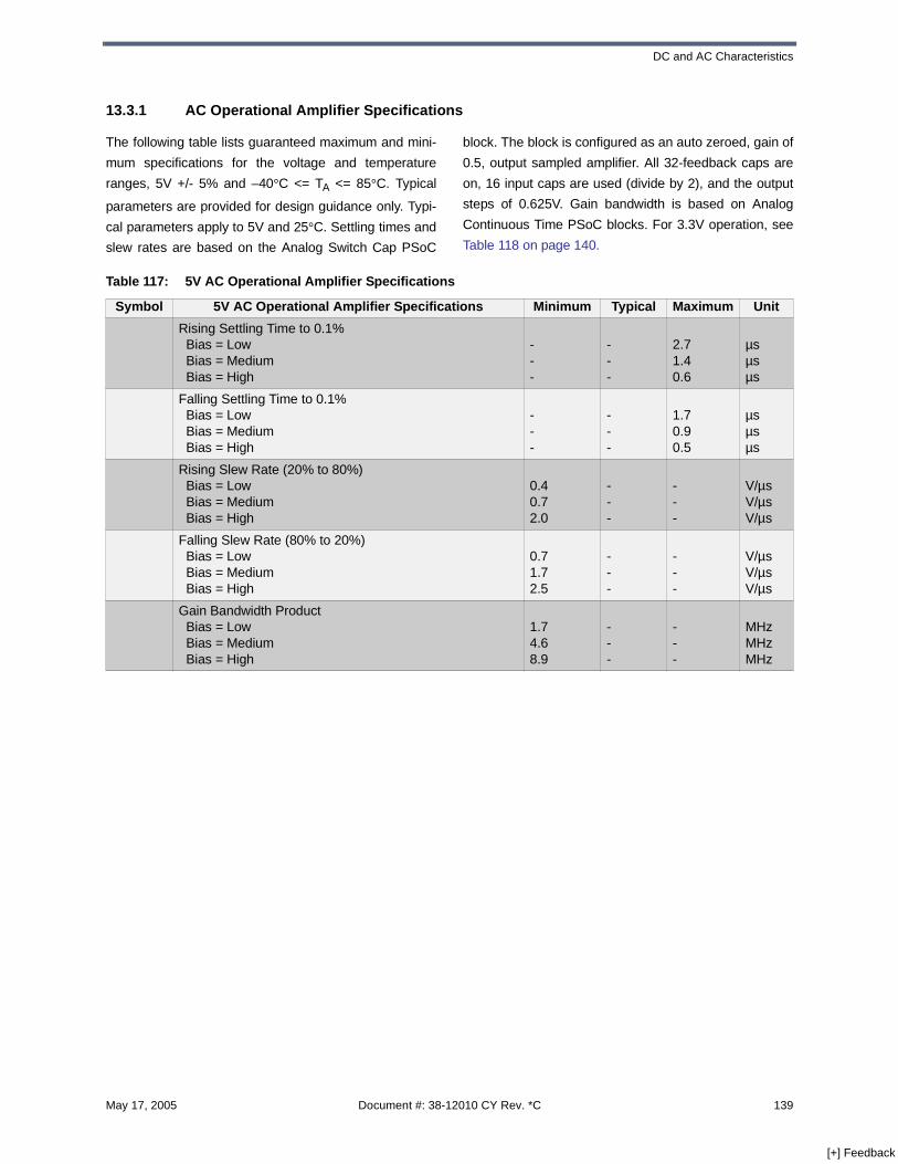
DC and AC Characteristics
13.3.1 AC Operational Amplifier Specifications
The following table lists guaranteed maximum and mini-
mum specifications for the voltage and temperature
ranges, 5V +/- 5% and –40°C <= TA <= 85°C. Typical
parameters are provided for design guidance only. Typi-
cal parameters apply to 5V and 25°C. Settling times and
slew rates are based on the Analog Switch Cap PSoC
block. The block is configured as an auto zeroed, gain of
0.5, output sampled amplifier. All 32-feedback caps are
on, 16 input caps are used (divide by 2), and the output
steps of 0.625V. Gain bandwidth is based on Analog
Continuous Time PSoC blocks. For 3.3V operation, see
Table 118 on page 140.
Table 117: 5V AC Operational Amplifier Specifications
Symbol 5V AC Operational Amplifier Specifications Minimum Typical Maximum Unit
Rising Settling Time to 0.1% Bias = Low Bias = Medium Bias = High
---
---
2.71.40.6
µsµsµs
Falling Settling Time to 0.1% Bias = Low Bias = Medium Bias = High
---
---
1.70.90.5
µsµsµs
Rising Slew Rate (20% to 80%) Bias = Low Bias = Medium Bias = High
0.40.72.0
---
---
V/µsV/µsV/µs
Falling Slew Rate (80% to 20%) Bias = Low Bias = Medium Bias = High
0.71.72.5
---
---
V/µsV/µsV/µs
Gain Bandwidth Product Bias = Low Bias = Medium Bias = High
1.74.68.9
---
---
MHzMHzMHz
May 17, 2005 Document #: 38-12010 CY Rev. *C 139
[+] Feedback

CY8C25122/CY8C26233/CY8C26443/CY8C26643 Device Family Data Sheet
Table 118: 3.3V AC Operational Amplifier Specifications
Symbol 3.3V AC Operational Amplifier Specifications Minimum Typical Maximum Unit
Rising Settling Time to 0.1% Bias = Low Bias = Medium Bias = High
---
---
3.01.61.5
µsµsµs
Falling Settling Time to 0.1% Bias = Low Bias = Medium Bias = High
---
---
2.61.71.6
µsµsµs
Rising Slew Rate (20% to 80%) Bias = Low Bias = Medium Bias = High
0.20.30.3
---
---
V/µsV/µsV/µs
Falling Slew Rate (80% to 20%) Bias = Low Bias = Medium Bias = High
0.30.30.3
---
---
V/µsV/µsV/µs
Gain Bandwidth Product Bias = Low Bias = Medium Bias = High
1.54.48.7
---
---
MHzMHzMHz
140 Document #: 38-12010 CY Rev. *C May 17, 2005
[+] Feedback

DC and AC Characteristics
13.3.2 AC Analog Output Buffer Specifications
The following table lists guaranteed maximum and mini-
mum specifications for the voltage and temperature
ranges, 5V +/- 5% and –40°C <= TA <= 85°C. Typical
parameters are provided for design guidance only. Typi-
cal parameters apply to 5V and 25°C. For 3.3V opera-
tion, see Table 120 on page 142.
Table 119: 5V AC Analog Output Buffer Specifications
Symbol 5V AC Analog Output Buffer Specifications Minimum Typical Maximum Unit
Rising Settling Time to 0.1%, 1V Step, 100pF Load Bias = Low Bias = High
--
--
2.52.5
µsµs
Falling Settling Time to 0.1%, 1V Step, 100pF Load Bias = Low Bias = High
--
--
2.22.2
µsµs
Rising Slew Rate (20% to 80%), 1V Step, 100pF Load Bias = Low Bias = High
.9
.9--
--
V/µsV/µs
Falling Slew Rate (80% to 20%), 1V Step, 100pF Load Bias = Low Bias = High
.9
.9--
--
V/µsV/µs
Small Signal Bandwidth, 20mVpp, 3dB BW, 100pF Load Bias = Low Bias = High
1.51.5
--
--
MHzMHz
Large Signal Bandwidth, 1Vpp, 3dB BW, 100pF Load Bias = Low Bias = High
600600
--
--
kHzkHz
May 17, 2005 Document #: 38-12010 CY Rev. *C 141
[+] Feedback
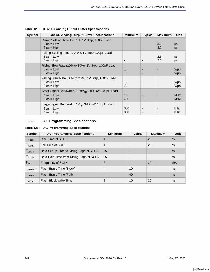
CY8C25122/CY8C26233/CY8C26443/CY8C26643 Device Family Data Sheet
13.3.3 AC Programming Specifications
Table 120: 3.3V AC Analog Output Buffer Specifications
Symbol 3.3V AC Analog Output Buffer Specifications Minimum Typical Maximum Unit
Rising Settling Time to 0.1%, 1V Step, 100pF Load Bias = Low Bias = High
--
--
3.23.2
µsµs
Falling Settling Time to 0.1%, 1V Step, 100pF Load Bias = Low Bias = High
--
--
2.62.6
µsµs
Rising Slew Rate (20% to 80%), 1V Step, 100pF Load Bias = Low Bias = High
.5
.5--
--
V/µsV/µs
Falling Slew Rate (80% to 20%), 1V Step, 100pF Load Bias = Low Bias = High
.5
.5--
--
V/µsV/µs
Small Signal Bandwidth, 20mVpp, 3dB BW, 100pF Load Bias = Low Bias = High
1.31.3
--
--
MHzMHz
Large Signal Bandwidth, 1Vpp, 3dB BW, 100pF Load Bias = Low Bias = High
360360
--
--
kHzkHz
Table 121: AC Programming Specifications
Symbol AC Programming Specifications Minimum Typical Maximum Unit
Trsclk Rise Time of SCLK 1 - 20 ns
Tfsclk Fall Time of SCLK 1 - 20 ns
Tssclk Data Set up Time to Rising Edge of SCLK 25 - - ns
Thsclk Data Hold Time from Rising Edge of SCLK 25 - - ns
Fsclk Frequency of SCLK 2 - 20 MHz
Teraseb Flash Erase Time (Block) - 10 - ms
Terasef Flash Erase Time (Full) - 40 - ms
Twrite Flash Block Write Time 2 10 20 ms
142 Document #: 38-12010 CY Rev. *C May 17, 2005
[+] Feedback

Packaging Information
14.0 Packaging Information
Figure 37: 44-Lead Thin Plastic Quad Flat Pack A44
51-85064-B
May 17, 2005 Document #: 38-12010 CY Rev. *C 143
[+] Feedback

CY8C25122/CY8C26233/CY8C26443/CY8C26643 Device Family Data Sheet
Figure 38: 20-Pin Shrunk Small Outline Package O20
51-85077 *C
144 Document #: 38-12010 CY Rev. *C May 17, 2005
[+] Feedback

Packaging Information
Figure 39: 28-Lead (210-Mil) Shrunk Small Outline Package O28
Figure 40: 48-Lead Shrunk Small Outline Package O48
51-85079 *C
51-85061-C
May 17, 2005 Document #: 38-12010 CY Rev. *C 145
[+] Feedback
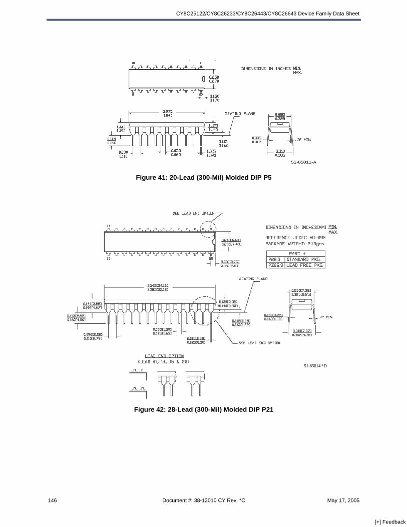
CY8C25122/CY8C26233/CY8C26443/CY8C26643 Device Family Data Sheet
Figure 41: 20-Lead (300-Mil) Molded DIP P5
Figure 42: 28-Lead (300-Mil) Molded DIP P21
51-85011-A
20-Lead(300-Mil)MoldedDIPP5
51-85014 *D
146 Document #: 38-12010 CY Rev. *C May 17, 2005
[+] Feedback

Packaging Information
Figure 43: 48-Lead (600-Mil) Molded DIP P25
Figure 44: 20-Lead (300-Mil) Molded SOIC S5
51-85020-A
48-Lead (600-Mil) Molded DIP P25
51-85024 *B
May 17, 2005 Document #: 38-12010 CY Rev. *C 147
[+] Feedback

CY8C25122/CY8C26233/CY8C26443/CY8C26643 Device Family Data Sheet
Figure 45: 28-Lead (300-Mil) Molded SOIC S21
Figure 46: 8-Lead (300-Mil) Molded DIP
51-85026 *C
0.115
0.100 BSC.
0.125
0.055
0.014
0.015 MIN.
0.145
0.070
0.022
0.140
SEATINGPLANE
0.380
0.240
0.180 MAX.
0.300
0.430 MAX.
0.325
0.0080°-10°0.015
0.390
0.260
DIMENSIONS IN INCHES MIN.MAX.
PIN 1 ID
HTN 04/03/97
8LD (300 MIL) PDIP PKG OUTLINE
P08.3 51-85075 *A
8 Lead (300 Mil) PDIP
14
5 8
CYPRESS
+-
-+
+- -+
.XXXX
.XXX
.XX
PART NO.
UNLESS OTHERWISE SPECIFIED
REVDWG NOSIZE
TITLE
MATERIAL
ANGLESDECIMALS
STANDARD TOLERANCES ON:
ALL DIMENSIONS ARE IN INCHES
APPROVED BY
APPROVED BY
CHK BY
DRAWN
DESIGNED BY
DATE
DATE
DATE
DATE
DATE
SEMICONDUCTOR
A
148 Document #: 38-12010 CY Rev. *C May 17, 2005
[+] Feedback

Packaging Information
14.1 Thermal Impedances per Package
Table 122: Thermal Impedances
Package Typical ΘJA
8 PDIP 121 C/W
20 PDIP 107 C/W
20 SOIC 80 C/W
20 SSOP 116 C/W
28 PDIP 68 C/W
28 SOIC 72 C/W
28 SSOP 95 C/W
48 PDIP 70 C/W
48 SSOP 69 C/W
44 TQFP 58 C/W
May 17, 2005 Document #: 38-12010 CY Rev. *C 149
[+] Feedback
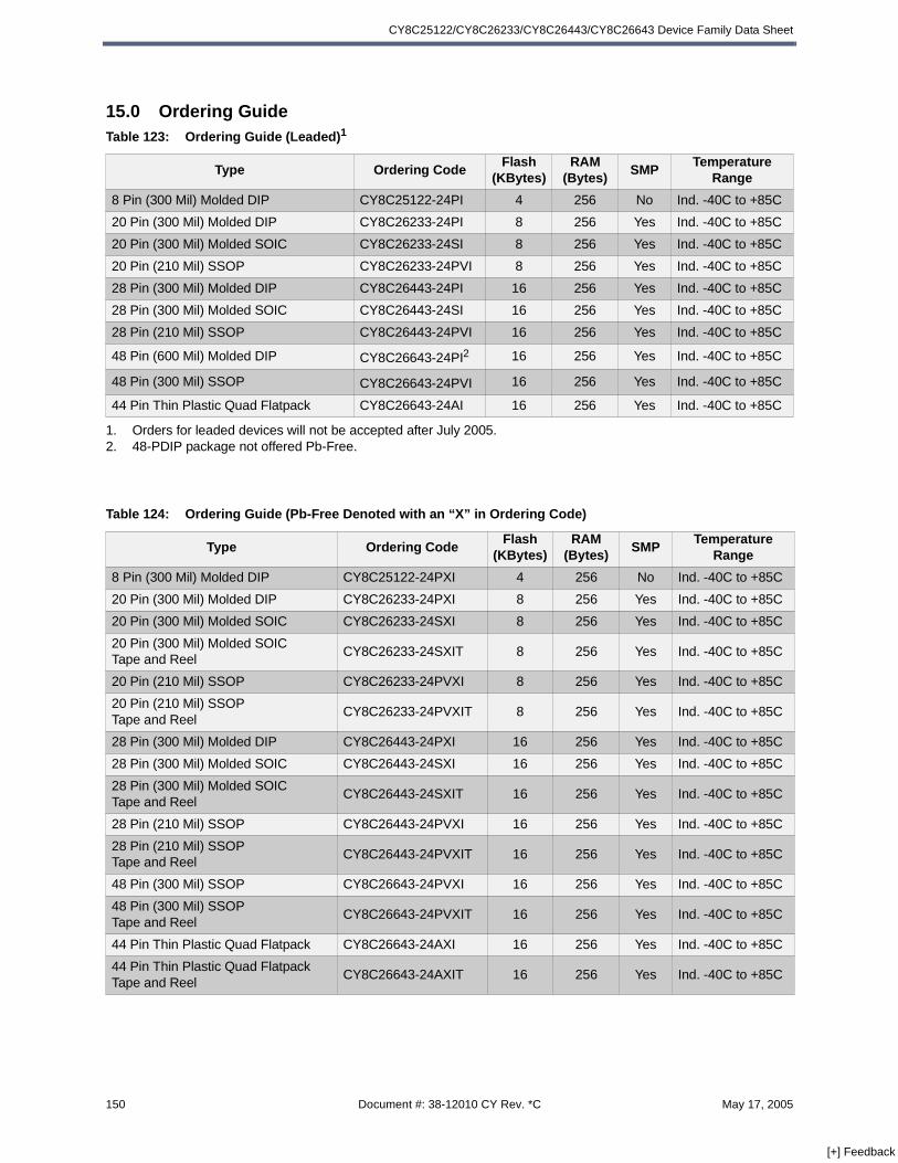
CY8C25122/CY8C26233/CY8C26443/CY8C26643 Device Family Data Sheet
15.0 Ordering Guide Table 123: Ordering Guide (Leaded)1
1. Orders for leaded devices will not be accepted after July 2005.
Type Ordering CodeFlash
(KBytes)RAM
(Bytes)SMP
Temperature Range
8 Pin (300 Mil) Molded DIP CY8C25122-24PI 4 256 No Ind. -40C to +85C
20 Pin (300 Mil) Molded DIP CY8C26233-24PI 8 256 Yes Ind. -40C to +85C
20 Pin (300 Mil) Molded SOIC CY8C26233-24SI 8 256 Yes Ind. -40C to +85C
20 Pin (210 Mil) SSOP CY8C26233-24PVI 8 256 Yes Ind. -40C to +85C
28 Pin (300 Mil) Molded DIP CY8C26443-24PI 16 256 Yes Ind. -40C to +85C
28 Pin (300 Mil) Molded SOIC CY8C26443-24SI 16 256 Yes Ind. -40C to +85C
28 Pin (210 Mil) SSOP CY8C26443-24PVI 16 256 Yes Ind. -40C to +85C
48 Pin (600 Mil) Molded DIP CY8C26643-24PI2
2. 48-PDIP package not offered Pb-Free.
16 256 Yes Ind. -40C to +85C
48 Pin (300 Mil) SSOP CY8C26643-24PVI 16 256 Yes Ind. -40C to +85C
44 Pin Thin Plastic Quad Flatpack CY8C26643-24AI 16 256 Yes Ind. -40C to +85C
Table 124: Ordering Guide (Pb-Free Denoted with an “X” in Ordering Code)
Type Ordering CodeFlash
(KBytes)RAM
(Bytes)SMP
Temperature Range
8 Pin (300 Mil) Molded DIP CY8C25122-24PXI 4 256 No Ind. -40C to +85C
20 Pin (300 Mil) Molded DIP CY8C26233-24PXI 8 256 Yes Ind. -40C to +85C
20 Pin (300 Mil) Molded SOIC CY8C26233-24SXI 8 256 Yes Ind. -40C to +85C
20 Pin (300 Mil) Molded SOICTape and Reel
CY8C26233-24SXIT 8 256 Yes Ind. -40C to +85C
20 Pin (210 Mil) SSOP CY8C26233-24PVXI 8 256 Yes Ind. -40C to +85C
20 Pin (210 Mil) SSOPTape and Reel
CY8C26233-24PVXIT 8 256 Yes Ind. -40C to +85C
28 Pin (300 Mil) Molded DIP CY8C26443-24PXI 16 256 Yes Ind. -40C to +85C
28 Pin (300 Mil) Molded SOIC CY8C26443-24SXI 16 256 Yes Ind. -40C to +85C
28 Pin (300 Mil) Molded SOICTape and Reel
CY8C26443-24SXIT 16 256 Yes Ind. -40C to +85C
28 Pin (210 Mil) SSOP CY8C26443-24PVXI 16 256 Yes Ind. -40C to +85C
28 Pin (210 Mil) SSOPTape and Reel
CY8C26443-24PVXIT 16 256 Yes Ind. -40C to +85C
48 Pin (300 Mil) SSOP CY8C26643-24PVXI 16 256 Yes Ind. -40C to +85C
48 Pin (300 Mil) SSOPTape and Reel
CY8C26643-24PVXIT 16 256 Yes Ind. -40C to +85C
44 Pin Thin Plastic Quad Flatpack CY8C26643-24AXI 16 256 Yes Ind. -40C to +85C
44 Pin Thin Plastic Quad FlatpackTape and Reel
CY8C26643-24AXIT 16 256 Yes Ind. -40C to +85C
150 Document #: 38-12010 CY Rev. *C May 17, 2005
[+] Feedback

Document Revision History
16.0 Document Revision HistoryTable 125: Document Revision History
Document Title: CY8C25122, CY8C26233, CY8C26443, CY8C26643 Device Data Sheet for Silicon Revision DDocument Number: 38-12010Revision ECN # Issue Date Origin of Change Description of Change
** 116628 6/17/2002CMS Cypress Man-agement. New Sili-con Revision.
New document to CY Document Control (Revision **). Revision 3.20 for CMS customers.
*A 127231 5/22/2003 HMT. Implementing new error tracking and document release procedure. Changes in red for Document #: 38-12010 CY Rev. *A CMS Rev. 3.20a. Changes include:--Bit 6 of the VLT_CR register is RW. Should be changed from "RW" to "--." --Analog Output Buffer Control Register ABF_CR Read/Write in Bank 1 table was corrected to Write Only. --Rewrite of section 10.4 Analog Reference Control .--AC Char. Spec. table changed .080 to 80 in "Vdd Rise Rate at Power Up." On features pg. 2, changed "Up to 10 bit DAC" to "Up to 8 bit DAC." --Adding temp. spec. for 24 MHz at beginning of AC/DC Characteristics section and Absolute Maximum Value table.--In AC Operating Spec. table fixed footnote for Out-put Rise Time minimum.--In AC Operating Spec. table fixed value for External Reset Pulse Width.--Changed uS to us units in tables.--New intro. --In the Analog Reference Control Register, ARF_CR, state 100 for bits 2:0should be described as "All Analog Off.“--Rework title pgs.
*B 127231 5/22/2003 HMT. Several updates including Thermal Impedances table, 8 PDIP diagram and company address. OSC_CR0 register name.
*C 362598 See ECN HMT. Add Pb-Free table. Add “Not Recommended for New Designs“ banner. Update package revisions. Fix reg-ister typo’s.
Distribution: External/PublicPosting: None
May 17, 2005 Document #: 38-12010 CY Rev. *C 151
[+] Feedback