8-bit arithmetic logic unit design...
TRANSCRIPT
8-bit Arithmetic Logic Unit Design Report Fang, Hongxia
Zhang, Zhaobo
Zhao, Yang
Zhong, Wei
Instructor: James Morizio
2007-12-09
ECE 261 Project

8bit ALU Design Report
Outline - Generalization - Function - Structure - Assignment - Design results - Summary
Generalization
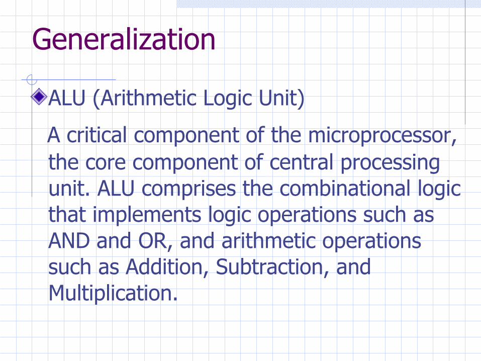
ALU (Arithmetic Logic Unit)
A critical component of the microprocessor, the core component of central processing unit. ALU comprises the combinational logic that implements logic operations such as AND and OR, and arithmetic operations such as Addition, Subtraction, and Multiplication.

Generalization
A and B: N-bit InputsResult: N-bit OutputOp: ALU operation, K-bit means
could support maximum 2k operation
Zero, CarryOut, Overflow: 1-bit flagA
B
N
N
N Result
K
Op
CarryOutZero
Overflow
ALU
ALU symbol
Function
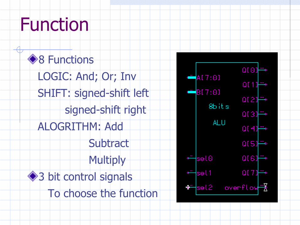
8 Functions LOGIC: And; Or; Inv SHIFT: signed-shift left signed-shift right ALOGRITHM: Add Subtract Multiply
3 bit control signals To choose the function

Structure
Schematic – 7 components

Structure
Layout - place
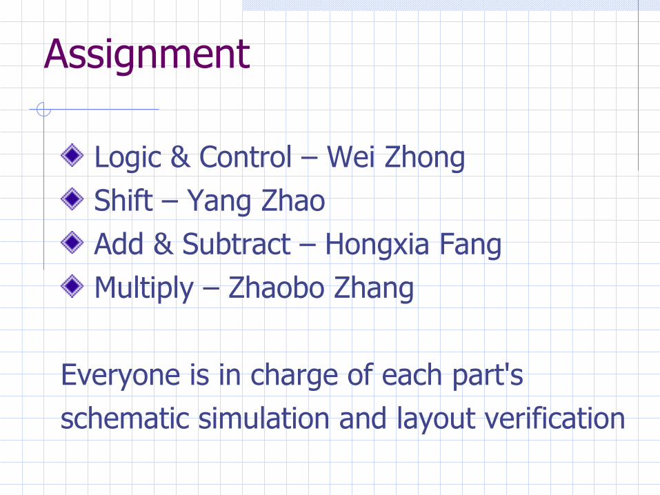
Assignment
Logic & Control – Wei Zhong Shift – Yang Zhao Add & Subtract – Hongxia Fang Multiply – Zhaobo Zhang
Everyone is in charge of each part's schematic simulation and layout verification

Design results
8 to 1 MUX - Using compound gate to realize 2 to 1
MUX
٠ ١Y D S D S= +

8 to 1 Mux

Set A0=1, A1~A7=0. whenS2S1S0=000, Out=1

8-bit 8 to 1 Mux

Layout of 1-bit Mux81 2-bit Mux81

Logic Function8-bit AND

Simulation for 8bit input AND Input A[7:0]=01010101, B[7:0]=10101010, Q[7:0]=00000000

8bit OR
Logic Function

Simulation for 8bit input OR Input A[7:0]=01010101, B[7:0]=10101010, Q[7:0]=11111111

Simulation for 8bit input AND & OR
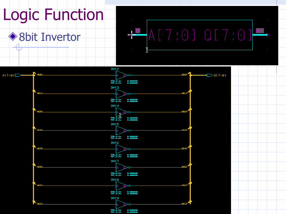
Logic Function8bit Invertor

Simulation for 8bit input OR Input A[7:0]=01010101, Q[7:0]=10101010

Signed-Shift Right Schematic

Simulation for Signed-shift right S0S1S2=010, connect A0 to extra bit, shift A7~A0=00101011 right for 2
bits, the output R7~R0=11001010

Signed-shift right Layout consist of 24 2-input MUX, using Metal 1 and Metal 2 interconnects

Signed-shift left Schematic
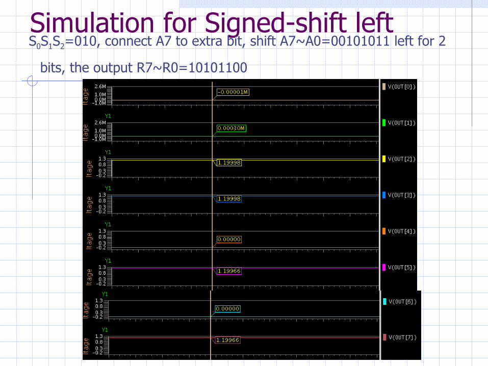
Simulation for Signed-shift left S0S1S2=010, connect A7 to extra bit, shift A7~A0=00101011 left for 2
bits, the output R7~R0=10101100

Signed-shift left Layout consist of 24 2-input MUX, using Metal 1 and Metal 2 interconnects

27
8-bit ripple Adder schematic

28
8-bit ripple Add-sub schematic
29
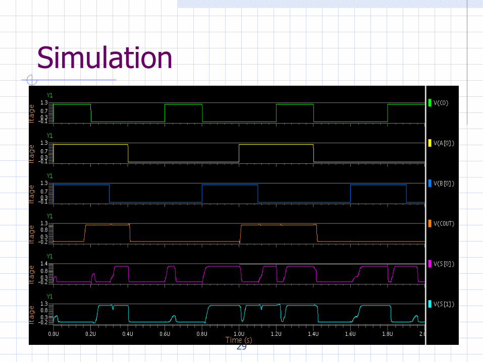
Simulation

30
1-bit full adder layout

31
8-bit ripple adder layout (part)

32
8-bit add-sub layout (part)

4-bit Booth Multiplier
Schematic
4-bit Booth Multiplier
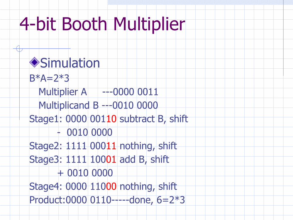
SimulationB*A=2*3 Multiplier A ---0000 0011 Multiplicand B ---0010 0000Stage1: 0000 00110 subtract B, shift - 0010 0000Stage2: 1111 00011 nothing, shiftStage3: 1111 10001 add B, shift + 0010 0000Stage4: 0000 11000 nothing, shiftProduct:0000 0110-----done, 6=2*3

4-bit Booth MultiplierStage1 out-11110001 stage2 out-11111000
Stage3 out-00001100 stage4 out-00000110

4-bit Booth Multiplier
Layout

Summary
We successfully design 8-bit ALU, supporting 4-bit multiplication. The design has a right simulation result and passes the DRC and LVS verificationFinal chip:
4464 transistors S=2mm*2mm