pci express v3.0 product guide - japan.xilinx.com
TRANSCRIPT

Versal ACAP CPM Mode forPCI Express v3.0
Product GuideVivado Design Suite
PG346 (v3.0) November 9, 2021
Xilinx is creating an environment where employees, customers, andpartners feel welcome and included. To that end, we’re removing non-inclusive language from our products and related collateral. We’velaunched an internal initiative to remove language that could excludepeople or reinforce historical biases, including terms embedded in oursoftware and IPs. You may still find examples of non-inclusivelanguage in our older products as we work to make these changes andalign with evolving industry standards. Follow this link for moreinformation.

Table of ContentsChapter 1: Overview......................................................................................................4
Navigating Content by Design Process.................................................................................... 4Introduction to the CPM4...........................................................................................................5Use Modes..................................................................................................................................10Limitations..................................................................................................................................16Licensing and Ordering............................................................................................................ 17
Chapter 2: Product Specification......................................................................... 18Minimum Device Requirements.............................................................................................. 18Port Descriptions.......................................................................................................................18Register Space........................................................................................................................... 80
Chapter 3: Designing with the Core................................................................... 82Clocking...................................................................................................................................... 82Resets..........................................................................................................................................84Tandem Configuration..............................................................................................................84
Chapter 4: Design Flow Steps.................................................................................92Customizing and Generating the CIPS IP Core......................................................................92
Appendix A: GT Selection and Pin Planning for CPM4............................120CPM4 GT Selection.................................................................................................................. 121CPM4 Additional Considerations...........................................................................................123GT Locations............................................................................................................................ 124
Appendix B: Debugging...........................................................................................128Finding Help on Xilinx.com.................................................................................................... 128PCIe Link Debug Enablement................................................................................................ 129
Appendix C: Migrating............................................................................................. 136Ports..........................................................................................................................................136GT Locations............................................................................................................................ 138
PG346 (v3.0) November 9, 2021 www.xilinx.comCPM Mode for PCI Express 2Send Feedback

Clocking.................................................................................................................................... 138Reset......................................................................................................................................... 139Features....................................................................................................................................139Attributes..................................................................................................................................141
Appendix D: Additional Resources and Legal Notices........................... 142Xilinx Resources.......................................................................................................................142Documentation Navigator and Design Hubs...................................................................... 142References................................................................................................................................143Revision History.......................................................................................................................143Please Read: Important Legal Notices................................................................................. 144
PG346 (v3.0) November 9, 2021 www.xilinx.comCPM Mode for PCI Express 3Send Feedback

Chapter 1
Overview
Navigating Content by Design ProcessXilinx® documentation is organized around a set of standard design processes to help you findrelevant content for your current development task. All Versal® ACAP design process DesignHubs and the Design Flow Assistant materials can be found on the Xilinx.com website. Thisdocument covers the following design processes:
• System and Solution Planning: Identifying the components, performance, I/O, and datatransfer requirements at a system level. Includes application mapping for the solution to PS,PL, and AI Engine. Topics in this document that apply to this design process include:
• Introduction to the CPM4
• Use Modes
• Embedded Software Development: Creating the software platform from the hardwareplatform and developing the application code using the embedded CPU. Also covers XRT andGraph APIs. The topic in this document that applies to this design process include:
• Register Space
• Host Software Development: Developing the application code, accelerator development,including library, XRT, and Graph API use. The topic in this document that applies to thisdesign process include:
• Register Space
• Hardware, IP, and Platform Development: Creating the PL IP blocks for the hardwareplatform, creating PL kernels, functional simulation, and evaluating the Vivado® timing,resource use, and power closure. Also involves developing the hardware platform for systemintegration. Topics in this document that apply to this design process include:
• Chapter 4: Design Flow Steps
• Appendix A: GT Selection and Pin Planning for CPM4
• PCIe Link Debug Enablement
Chapter 1: Overview
PG346 (v3.0) November 9, 2021 www.xilinx.comCPM Mode for PCI Express 4Send Feedback

Introduction to the CPM4The integrated block for PCIe® Rev. 4.0 with DMA and CCIX Rev. 1.0 (CPM4) consists of twoPCIe® controllers, DMA features, CCIX features, and network on chip (NoC) integration. TheVersal® ACAP CPM Mode for PCI Express enables direct access to the two high-performance,independently customizable PCIe controllers. The CPM4 uses up to 16 Versal device GTYchannels over the XPIPE. Application designs can also interface to the CPM4 with soft logic andclocking resources in the programmable logic. All feature references are applicable to bothinstances of CPM4 PCIe controllers, with the following exceptions:
• CPM4 PCIe Controller 0 supports up to x16 operation, and CPM4 PCIe Controller 1 supportsup to x8 operation.
• CPM4 PCIe Controller 1 with up to x8 support is available only when CPM4 PCIe Controller 0is configured with 8 lanes or fewer.
• The CPM4 DMA features are supported only with CPM4 PCIe Controller 0. For moreinformation about CPM4 DMA features, see the Versal ACAP CPM DMA and Bridge Mode forPCI Express Product Guide (PG347).
Chapter 1: Overview
PG346 (v3.0) November 9, 2021 www.xilinx.comCPM Mode for PCI Express 5Send Feedback

Figure 1: CPM4 Sub-Block for PCIe Function (CPM4 PCIE)
CPM4 PCIe Controller #1
CPM4 PCIe Controller #0
ARM(*) CoreSight I/F Module
AXI4-ST
DataLink
Layer
Mux
/Dem
ux
Physical Layer
CfgReg
Space
Integrated PCIe RAM
Clock &Reset
cfg
XPIPE Hard I/FUp to 2 Quads
Gen1 (2.5 GT/s) 16b@125 MHzGen2 (5.0 GT/s) 16b@250 MHzGen3 (8.0 GT/s) 16b@500 MHzGen4 (16.0 GT/s) 32b@500 MHz
TransactionLayer(VC0,
CCIX VC1)
APBBlock
Program-ming
Hard I/F
XPIP
EIM
InitCtrl
AXI4-ST
DataLink
Layer
Mux
/Dem
ux
CPM4 DMA
DMA Core
Physical Layer
CfgReg
Space
Integrated PCIe RAM
Clock &Reset
cfg
512b512b
512b
cfg
AXI4-ST TX
Integrated DMA RAM
AXI4-ST RX
512b
512bcfg
XPIPE Hard I/FUp to 4 Quads
Gen1 (2.5 GT/s) 16b@125 MHzGen2 (5.0 GT/s) 16b@250 MHzGen3 (8.0 GT/s) 16b@500 MHzGen4 (16.0 GT/s) 32b@500 MHz
TransactionLayer(VC0,
CCIX VC1)
PCIe Core Clock InPCIe Reset InGlobal Event Inputs
XPIP
EIM
Misc Port
512b
512b
AXI4-MM
Bridge
DMA
AXI4-MMSwitch
InitCtrl
XPIPEStaticSwitch
PS InternalHard I/F
Programming Register Space
512b
512bcfg
512b
256b
256b
256b
512b 512b
32b
attr_*0
dbg_0_0 dbg_0_1
attr_dma_*
AXI4-MMMaster1
AXI4-MMMaster0
AXI4-MMSlave0
Enhanced AXI4-ST + CFG
+ Fabric I/F
64/128/256/512b
62.5/125/250 MHz
CCIX TL Hard I/F #1256b
500/625/781.25 MHz
Enhanced AXI4-ST +
CFG + Misc DMA I/OsFabric I/F
64/128/256/512b
62.5/125/250 MHz
ToOn Chip NOC
Hard I/F62.5/125/
250/390.625/500
MHz
CCIX TL Hard I/F #0
256b500/625/
781.25 MHz
To On Chip NOC Hard I/F
32b AXI4-MM Lite (MCAP)
To On Chip NOC Hard I/F32b AXI4-MM Lite (MCAP)
attr_*1
dbg_1_0 dbg_1_1
32b
RX
TX
RX
TX
X22665-072320
Chapter 1: Overview
PG346 (v3.0) November 9, 2021 www.xilinx.comCPM Mode for PCI Express 6Send Feedback

The CPM4 PCIe controllers are designed to the PCI Express Base Specification Revision 4.0 andsupport the Gen4 data rate (16 GT/s per lane). They also support the Gen1 (2.5 GT/s per lane),Gen2 (5 GT/s per lane) and Gen3 (8 GT/s per lane) data rates, and can interoperate withcomponents that are compliant with all versions of the PCI Express Base Specification.
The CPM4 PCIe controllers are available through the Vivado IP catalog in the Vivado IntegratedDesign Environment (IDE). The combination of the CPM4 PCIe controllers, the GTY, and clockingimplement all layers of the PCI Express protocol, and the configuration space and controller.
Protocol LayersThe layers of the protocol are the AXI4-Stream layer, the transaction layer, the data link layer andthe physical layer, and they are described below.
AXI4-Stream Layer
The AXI4-Stream layer implements Xilinx-specific requirements. In the transmit or outbounddirection, the AXI4 layer interfaces the transaction layer with two AXI4-Stream interfaces. In thereceive or inbound direction, the transaction layer output is forwarded to two AXI4-Streaminterfaces. Application designs can attach to the AXI4-Stream interfaces, exchange informationwith the Versal® ACAP CPM Mode for PCI Express encoded as a Xilinx-specific streamingprotocol implementation, and run on top of the industry standard AXI4-Stream interface. TheCPM4 PCIe controllers support management of up to 256 (extended tag) or 768 (10 bit Tag)outstanding customer initiated read requests, as part of the streaming protocol. The AXI4-Streamlayer supports:
• Reception and transmission of address translation services (ATS) invalid requests, ATS invalidcompletions, ATS page requests and ATS PRG response message TLPs, which enable ATS tobe implemented in the fabric logic.
• AXI4-Stream interface widths of 64 bits, 128 bits, 256 bits and 512 bits.
Transaction Layer
The transaction layer is the upper layer of the PCI Express architecture, and its primary functionis to accept, buffer, and forward transaction layer packets (TLPs). TLPs communicate informationwith the use of memory, I/O, configuration, and message transactions. To maximize the efficiencyof communication between devices, the transaction layer enforces PCI-compliant transactionordering rules and supports relaxed ordering (RO) of received transactions. The transaction layeralso manages TLP buffer space through credit-based flow control. The transaction layerimplements built-in tag management for transmitted non-posted transactions. It also implementscut-through forwarding of transactions in the transmit (or outbound) direction.
Chapter 1: Overview
PG346 (v3.0) November 9, 2021 www.xilinx.comCPM Mode for PCI Express 7Send Feedback

CCIX Transaction Layer
The Cache Coherent Interconnect for Accelerators (CCIX) transaction layer requirements areimplemented by the optional virtual channel 1 (VC1) in the design. Note that VC1 storage is inaddition to the PCI Express-compliant virtual channel 0 (VC0) storage. The CCIX transaction layerinterfaces with the CCIX protocol layer is implemented externally to the PCIe ports over theCCIX transaction layer (ARM CXS) hard interface. For more information, see the Versal ACAP CPMCCIX Architecture Manual (AM016).
Data Link Layer
The data link layer acts as an intermediate stage between the transaction layer and the physicallayer. Its primary responsibility is to provide a reliable mechanism for the exchange of informationbetween two components on a link. This includes data exchange (TLPs), error detection andrecovery, initialization services and the generation and consumption of data link layer packets(DLLPs). DLLPs are used to transfer information between data link layers of two directlyconnected components on the link. DLLPs convey information, such as power management, flowcontrol, and TLP acknowledgments. The data link layer supports 32 kilobyte replay buffers andthe feature DLLP.
Physical Layer
The physical layer interfaces the data link layer with signaling technology for link datainterchange, and is subdivided into the logical sub-block and the electrical sub-block.
• The logical sub-block frames and de-frames TLPs and DLLPs. It also implements the linktraining and status state machine (LTSSM), which handles link initialization, training, andmaintenance. Scrambling and descrambling of data (for Gen1/Gen2/Gen3/Gen4 operation) isalso performed in this sub-block.
• The electrical sub-block defines the input and output buffer characteristics that interface thedevice to the PCIe link. The physical layer also supports lane reversal (for multi-lane designs)and lane polarity inversion, as required by the PCI Express Base Specification 4.0 (https://www.pcisig.com/specifications).
Data exchange with the other components on the link occurs over the serial lines of one or moregigabit transceivers (GTs), which expose parallel interfaces at lower clock frequencies to the PCIecontroller. For Gen1, Gen2, Gen3 and Gen4 operation, the physical layer is up-configurationcapable in the downstream port mode only.
StandardsThe CPM4 block adheres to the following standards:
• PCI Express Base Specification 4.0 Version 1.0, and Errata updates (available at http://pcisig.com/specifications).
Chapter 1: Overview
PG346 (v3.0) November 9, 2021 www.xilinx.comCPM Mode for PCI Express 8Send Feedback

• Cache Coherent Interconnect for Accelerators (CCIX) Transport Specification 1.0 (available at http://www.ccixconsortium.com).
Features• Support for the following PCI Express architecture components:
○ PCI Express Endpoint, Legacy Endpoint
○ Root Port
○ Switch Upstream and Downstream Ports
• 2.5 GT/s, 5.0 GT/s and 8.0 GT/s line rates with x1, x2, x4, x8, and x16 lane operation.
• 16.0 GT/s line rate with x1, x2, x4, x8 lane operation.
• CCIX support in PCI Express and EDR PHY Modes
○ PCI Express support for Gen4x4, and Gen4x8
• Advanced Error Reporting (AER) and End-to-End CRC (ECRC)
• Two PCI Express virtual channels
○ One PCI Express compliant virtual channel, eight traffic classes
○ One CCIX compliant virtual channel
• Support for multiple functions and Single-Root IO Virtualization (SR-IOV)
○ Up to 4 physical functions
○ Up to 252 virtual functions
• Built-in lane reversal and receiver lane-lane de-skew
• 3 x 64-bit or 6 x 32-bit Base Address Registers (BARs) that are fully configurable
○ Expansion ROM BAR supported
• All Interrupt types are supported:
○ INTx
○ 32 multi-vector MSI capability
○ MSI-X capability with up to 2048 vectors with optional built-in vector tables
• Features that enable high-performance applications include:
○ AXI4-Stream TLP Straddle on Requester Completion Interface
○ Address Translation Services (ATS) and Page Request Interface (PRI) Messaging
○ Atomic Operation Transactions Support
Chapter 1: Overview
PG346 (v3.0) November 9, 2021 www.xilinx.comCPM Mode for PCI Express 9Send Feedback

○ Transaction Tag Scaling as Completer
○ Flow Control Scaling
Use ModesAll design use modes support Endpoint, Legacy Endpoint, and Root Port configurations.
PCI Express Endpoint Use ModesIllustrative Example of Basic Bus Mastering Endpoint
By far the most common use of the Versal® ACAP CPM Mode for PCI Express is to construct abus mastering Endpoint using a CPM PCIe controller. This use model is applicable to mostapplications that interface the Endpoint port on the ACAP (on an add-in card) to a root complexor that switch downstream port through a PCI Express connector. The following figure shows ablock diagram of the bus mastering Endpoint use case.
Chapter 1: Overview
PG346 (v3.0) November 9, 2021 www.xilinx.comCPM Mode for PCI Express 10Send Feedback

Figure 2: Basic PCI Express Bus Mastering Endpoint Use Case
Initiator Interface
TX
A R B I T E R
Mem
Wr
CplD
RX D
ATA
TX D
ATA
Bus Mastering (DMA) Logic
Bridge to User Application
Mem
Rd
Mem
Rd/
Wr
Control & Status Registers
RX
CplD
PCIe
CPM PCIe Controller
CONTROL LOGIC
Mem
Rd
Mem
Wr
D E M U X
CplD
CplD
Completer Interfaces Requester Interfaces
X22666-071620
Chapter 1: Overview
PG346 (v3.0) November 9, 2021 www.xilinx.comCPM Mode for PCI Express 11Send Feedback

PCI Express Two Function Endpoint
The following figure shows the architecture of a two-function Endpoint design. The CPM PCIeController is configured to enable two built-in function configuration spaces. This use caseenables the application device driver to access and control two distinct applicationsindependently. The user logic implements the DMA, control registers and applications.
Figure 3: Illustrative Example of Two Function Endpoint Use Case
FUN0
Application Function #0
Arbiter/Demux
CPM PCIe Controller
DMA
ControlRegs
TXBuf
RXBuf
FUN1
ControlRegs
TXBuf
RXBuf
ApplicationFunction #1
X22667-071620
Chapter 1: Overview
PG346 (v3.0) November 9, 2021 www.xilinx.comCPM Mode for PCI Express 12Send Feedback

PCI Express Endpoint with SR-IOV
The following figure shows the CPM PCIe Controller configured as a SR-IOV capable Endpoint,interfacing with the user design. This use case addresses requirements for up to four physical and252 virtual functions, and minimizes the soft logic requirement to implement an SR-IOVEndpoint.
Figure 4: Illustrative Example of Endpoint with SR-IOV Use Case
VM1VM0
VF0
CPM PCIe Controller
DMA
ControlRegs
TXBuf
RXBuf
VF1
ControlRegs
TXBuf
RXBuf
Application
PF Driver
Guest OSApplication
RXBuf
TXBuf
VF Driver
PF
Host
PCIe Link
VMM
X22668-071620
Chapter 1: Overview
PG346 (v3.0) November 9, 2021 www.xilinx.comCPM Mode for PCI Express 13Send Feedback

PCI Express Endpoint with AXI4 Memory Mapped Interface
This use case describes a PCI Express Endpoint functional unit that implements AXI4 MemoryMapped (AXI-MM) interfaces. This functional block implements a soft logic bridge between thenative AXI4-Stream interface on the CPM PCIe controller and AXI4 Memory Mappedinterconnect.
PCI Express Endpoint Using Tandem PROM
This use case addresses the ability to configure the ACAP in two stages and bring up the PCIExpress protocol in less than 100 ms after power to the ACAP is stable. This is accomplishedthrough a staged configuration flow.
PCI Express Endpoint Using Tandem PCIe
This use case addresses the ability to initially load fully configurable PCI Express protocolsolution from a small external ROM, so as to meet the 100 ms configuration requirement. A PCIelink is formed with a Root Complex or Switch component, which is subsequently used todownload the design that configures the rest of the ACAP. In this case the PCIe link is used bythe user application. This is accomplished through a staged configuration flow.
PCI Express Root Port Use ModeBasic PCI Express Root Complex Use Case
The following figure shows a PCI Express Root Complex in the simplest form consisting of a PCIExpress Root Port to an AXI4 memory mapped bridge interfaced with the interconnect. Theinterconnect consists of an Arm®-based processor system (PS) containing most of the criticalblocks such as CPU, memory controller and other important peripherals. One of the goals of thisuse case is to minimize ACAP soft logic requirements.
Chapter 1: Overview
PG346 (v3.0) November 9, 2021 www.xilinx.comCPM Mode for PCI Express 14Send Feedback

Figure 5: Basic PCI Express Root Complex Use Case
NEONSP, DP FPU
128-bit Vector DSP
Q-SPI1,2,4,8 bit
SLCRSystem Level
ControlRegisters
NEONSP, DP FPU
128-bit Vector DSP
Processor System (PS)
Parallel 8 bitNOR/SRAM
NAND 8, 16bit
USB DMAUSB DMAGigE DMAGigE DMASD DMASD DMA
GPIO x54, x64UARTUART
I2CI2CSPISPI
CANCAN
TTC/WDT
PJTAGCoresightTrace In
Trace OutCross Trigger
Reset
CLK / PLLCPU, DDR, IOU
ARM A932 KB I Cache32 KB D Cache
ARM A932 KB I Cache32 KB D Cache
IRQ20 I, 29 O SCU- Snoop Control Unit
L2Cache Memory
256 KB
Core Switch
OCMOn Chip Memory
256 KB
DMA8 channel Mem Switch
DDRMemory
Controller
DDR2DDR3
LPDDR2
16-bit32-bit
16- bit w/ECC
AXGM# x 2General Purpose32-bit AXI Master
AXGS# x 2General Purpose32-bit AXI Slave
AXCSAXI Coherent64-bit Slave
AXDS# x 4AXI Data
32/64
32- bit AXI64- bit AXI
FMIO
SystemController
M0128b
32b
AXI064bAXI1128b
S0
M064/128b
AXI MMPCIe
S64/128b
PCIe 4.0
GT
POR_BSRST_B
CLK
DDR
APBRegister Access
DAP
MIO[53:0]
SystemReset
SystemClock PCIe
Interrupts
CPM
PCAPProcessorConfig
M0S0
X22670-121420
Chapter 1: Overview
PG346 (v3.0) November 9, 2021 www.xilinx.comCPM Mode for PCI Express 15Send Feedback
LimitationsSpeed Change Related Issue
• Description: Repeated speed changes can result in the link not coming up to the intendedtargeted speed.
• Workaround: A follow-on attempt should bring the link back. In extremely rare scenarios a fullreboot might be required.
Link Autonomous Bandwidth Status (LABS) Bit
• Description: As a Root Complex when performing the link width/rate changes, the link widthchange works as expected. However, the PCIe protocol requires a LABS bit which is notgetting set after the link width/rate change.
Note: This is an informational bit and does not impact actual functionality.
• Workaround: Software / Application to ignore LABS bit as this is an informational bit and doesnot impact functionality.
Power Management - ASPM L1/L0s/PM D3
• Description:
1. Enabling ASPM L0s / ASPM L1 could show correctable errors being reported on link byboth Link partners (i.e., replay timer timeout, replay timer rollover, receiver error).
2. PCIe Endpoint device might also log errors when Configuration PM D3 transition requestcomes in during non-quiesced traffic mode.
• Workaround:
1. It is recommended that the application disables correctable error reporting or ignorescorrectable errors reported in event of link transitioned to ASPM L0s / ASPM L1.
2. For transition to D3Hot, software needs to make sure that the link is quiesced. To ensureMemory Write packets are finished, issue a Memory Read request to the same location.When the completion packet is received, it indicates that the link is quiesced and PM D3request can be issued.
ECAM Access
• Description: Repeated Link Rate changes might also result in ECAM access becomingunresponsive, applicable to both Root Port and End Point.
• In EP mode, the host may report Machine Check 0x12 Vector Trap if attempt is made toaccess multiple EP ECAM / Bridge Registers in this scenario.
Chapter 1: Overview
PG346 (v3.0) November 9, 2021 www.xilinx.comCPM Mode for PCI Express 16Send Feedback

• When PM D3 is also enabled and when the Pre-Read is done before the PM D3 sequenceis targeted to the EP ECAM space, the host might receive completion timeout for this readdue to this scenario.
• Workaround: Waiting for some time (in order of tens of milliseconds) after link rate beforeattempting any EP ECAM / Bridge access may help, recommendation for Pre-Read before PMD3 sequence is to target any valid EP address except EP ECAM space. In scenarios where thetransaction does not complete, a full reboot would be required.
Licensing and OrderingThis Xilinx® LogiCORE™ IP module is provided at no additional cost with the Xilinx Vivado®
Design Suite under the terms of the Xilinx End User License.
For more information about this Versal® ACAP CPM Mode for PCIe, visit the Versal® ACAP CPMMode for PCIe product web page.
Information about other Xilinx® LogiCORE™ IP modules is available at the Xilinx IntellectualProperty page. For information about pricing and availability of other Xilinx LogiCORE IP modulesand tools, contact your local Xilinx sales representative.
Chapter 1: Overview
PG346 (v3.0) November 9, 2021 www.xilinx.comCPM Mode for PCI Express 17Send Feedback

Chapter 2
Product Specification
Minimum Device RequirementsCPM4
CPM4 Gen4x16 configurations can only be enabled when using DMA mode, as described inVersal ACAP CPM DMA and Bridge Mode for PCI Express Product Guide (PG347). PCIe® controller-only mode does not support Gen4x16. The support is limited to Gen4x8.
Table 1: CPM4 Controller-Only Maximum Configurations (Versal Prime, Versal AI Core,Versal AI Edge)
Speed Grade -1 -1 -2 -2 -2 -3Voltage Grade L (0.70V) M (0.80V) L (0.70V) M (0.80V) H (0.88V) H (0.88V)
Gen1 (2.5 GT/s perlane)
x16 x16 x16 x16 x16 x16
Gen2 (5 GT/s per lane) x16 x16 x16 x16 x16 x16
Gen3 (8 GT/s per lane) x16 x16 x16 x16 x16 x16
Gen4 (16 GT/s perlane)
x8 x8 x8 x8 x81 x81
Notes:1. x16 configuration is available using CPM4 in DMA mode. For details, see Versal ACAP CPM DMA and Bridge Mode for PCI
Express Product Guide (PG347).
Port DescriptionsNote: All the ports in the description field of the table excludes pcie0/pcie1 appended to the port names asthe description is same for both. Please note that the pcie0* port name maps to pcie0* port names in thedescription field and pcie1* port name maps to pcie1* port names in the description field.
For example, the description for pcie0_m_axis_cq_tuser and pcie1_m_axis_cq_tuser states: These signals arevalid when m_axis_cq_tvalid is High. Here, pcie0_m_axis_cq_tuser is valid when pcie0_m_axis_cq_tvalid is High,and pcie1_m_axis_cq_tuser is valid when pcie1_m_axis_cq_tvalid is High.
Chapter 2: Product Specification
PG346 (v3.0) November 9, 2021 www.xilinx.comCPM Mode for PCI Express 18Send Feedback

AXI4-Stream Core Interfaces
64/128/256-Bit Interfaces
In addition to status and control interfaces, the core has four required AXI4-Stream interfacesused to transfer and receive transactions, which are described in this section.
Completer Request Interface
The Completer Request (CQ) interface are the ports through which all received requests from thelink are delivered to the user application. The following table defines the ports in the CQinterface of the core. In the Width column, DW denotes the configured data bus width (64, 128,or 256 bits).
Table 2: Completer Request Interface Port Descriptions
Port I/O Width Description
pcie0_m_axis_cq_tdatapcie1_m_axis_cq_tdata O DW
Transmit Data from the CQ Interface.Only the lower 128 bits are used when the interface widthis 128 bits, and only the lower 64 bits are used when theinterface width is 64 bits.Bits [255:128] are set permanently to 0 by the core whenthe interface width is configured as 128 bits, and bits[255:64] are set permanently to 0 when the interfacewidth is configured as 64 bits.
pcie0_m_axis_cq_tuserpcie1_m_axis_cq_tuser O 108
CQ User Data.This set of signals contains sideband information for thetransaction layer packets (TLP) being transferred. Thesesignals are valid when pcie(n)_m_axis_cq_tvalid is High.Table 3: Sideband Signal Descriptions inpcie(n)_m_axis_cq_tuser describes the individual signals inthis set.
pcie0_m_axis_cq_tlastpcie1_m_axis_cq_tlast O 1
TLAST indication for CQ Data.The core asserts this signal in the last beat of a packet toindicate the end of the packet. When a TLP is transferredin a single beat, the core sets this signal in the first beatof the transfer.
pcie0_m_axis_cq_tkeeppcie1_m_axis_cq_tkeep O DW/32
TKEEP indication for CQ Data.The assertion of bit i of this bus during a transferindicates to the user application that Dword i of thepcie(n)_m_axis_cq_tdata bus contains valid data. The coresets this bit to 1 contiguously for all Dwords starting fromthe first Dword of the descriptor to the last Dword of thepayload. Thus, pcie(n)_m_axis_cq_tdata is set to all 1s in allbeats of a packet, except in the final beat when the totalsize of the packet is not a multiple of the width of the databus (in both Dwords). This is true for both Dword-alignedand address-aligned modes of payload transfer.Bits [7:4] of this bus are set permanently to 0 by the corewhen the interface width is configured as 128 bits, andbits [7:2] are set permanently to 0 when the interfacewidth is configured as 64 bits.
Chapter 2: Product Specification
PG346 (v3.0) November 9, 2021 www.xilinx.comCPM Mode for PCI Express 19Send Feedback

Table 2: Completer Request Interface Port Descriptions (cont'd)
Port I/O Width Description
pcie0_m_axis_cq_tvalidpcie1_m_axis_cq_tvalid O 1
CQ Data Valid.The core asserts this output whenever it is driving validdata on the pcie(n)_m_axis_cq_tdata bus. The core keepsthe valid signal asserted during the transfer of a packet.The user application can pace the data transfer using thepcie(n)_m_axis_cq_tready signal.
pcie0_m_axis_cq_treadypcie1_m_axis_cq_tready I 1
CQ Data Ready.Activation of this signal by the user logic indicates to thecore that the user application is ready to accept data.Data is transferred across the interface when bothpcie(n)_m_axis_cq_tvalid and pcie(n)_m_axis_cq_tready areasserted in the same cycle.If the user application deasserts the ready signal whenpcie(n)_m_axis_cq_tvalid is High, the core maintains thedata on the bus and keeps the valid signal asserted untilthe user application has asserted the ready signal.
pcie0_cq_np_reqpcie1_cq_np_req I 2
This input is used by the user application to request thedelivery of a Non-Posted request. The core implements acredit-based flow control mechanism to control thedelivery of Non-Posted requests across the interface,without blocking Posted TLPs.This input to the core controls an internal credit count.The credit count is updated in each clock cycle based onthe setting of pcie(n)_cq_np_req[1:0] as follows:• 00: No change• 01: Increment by 1• 10 or 11: Reserved (bit [1] only applicable in 512-bit
interface)The credit count is decremented on the delivery of eachNon-Posted request across the interface. The coretemporarily stops delivering Non-Posted requests to theuser logic when the credit count is zero. It continues todeliver any Posted TLPs received from the link even whenthe delivery of Non-Posted requests has been paused.The user application can either set pcie_cq_np_req[1:0] ineach cycle based on the status of its Non-Posted requestreceive buffer, or can set it to 11 permanently if it doesnot need to exercise selective backpressure on Non-Posted requests.The setting of pcie(n)_cq_np_req[1:0] does not need to bealigned with the packet transfers on the completerrequest interface.
pcie0_cq_np_req_countpcie1_cq_np_req_count O 6
This output provides the current value of the credit countmaintained by the core for delivery of Non-Postedrequests to the user logic. The core delivers a Non-Postedrequest across the completer request interface only whenthis credit count is non-zero. This counter saturates at amaximum limit of 32.Because of internal pipeline delays, there can be severalcycles of delay between the user application providingcredit on the pcie(n)_cq_np_req[1:0] inputs and the PCIecore updating the pcie_cq_np_req_count output inresponse.This count resets on user_reset and de-assertion ofuser_lnk_up.
Chapter 2: Product Specification
PG346 (v3.0) November 9, 2021 www.xilinx.comCPM Mode for PCI Express 20Send Feedback

When PASID_CAP_ON is enabled then pcie(n)_m_axis_cq_tuser [107:85] pins areshared with cfg* ports. The following table provides more information.
Table 3: Sideband Signal Descriptions in pcie(n)_m_axis_cq_tuser
Bit Index Name Width Description
3:0 first_be[3:0] 4
Byte enables for the first Dword of the payload.This field reflects the setting of the First_BE bits in theTransaction-Layer header of the TLP. For Memory Reads andI/O Reads, these four bits indicate the valid bytes to be readin the first Dword. For Memory Writes and I/O Writes, thesebits indicate the valid bytes in the first Dword of thepayload. For Atomic Operations and Messages with apayload, these bits are set to all 1s.This field is valid in the first beat of a packet, that is, whensop and pcie(n)_m_axis_cq_tvalid are both High.
7:4 last_be[3:0] 4
Byte enables for the last Dword.This field reflects the setting of the Last_BE bits in theTransaction-Layer header of the TLP. For Memory Reads,these four bits indicate the valid bytes to be read in the lastDword of the block of data. For Memory Writes, these bitsindicate the valid bytes in the ending Dword of the payload.For Atomic Operations and Messages with a payload, thesebits are set to all 1s. For Memory Reads and Writes of oneDW transfers and zero length transfers, these bits should be0s.This field is valid in the first beat of a packet, that is, whensop and pcie(n)_m_axis_cq_tvalid are both High.
39:8 byte_en[31:0] 32
The user logic can optionally use these byte enable bits todetermine the valid bytes in the payload of a packet beingtransferred. The assertion of bit i of this bus during atransfer indicates that byte i of the pcie(n)_m_axis_cq_tdatabus contains a valid payload byte. This bit is not asserted fordescriptor bytes.Although the byte enables can be generated by user logicfrom information in the request descriptor (address andlength) as well as the settings of the first_be and last_besignals, you can use these signals directly instead ofgenerating them from other interface signals.When the payload size is more than two Dwords (eightbytes), the one bit on this bus for the payload is alwayscontiguous. When the payload size is two Dwords or less,the one bit can be non-contiguous.For the special case of a zero-length memory writetransaction defined by the PCI Express specifications, thebyte_en bits are all 0s when the associated one-DW payloadis being transferred.Bits [31:16] of this bus are set permanently to 0 by the corewhen the interface width is configured as 128 bits, and bits[31:8] are set permanently to 0 when the interface width isconfigured as 64 bits.
40 sop 1
Start of packet.This signal is asserted by the core in the first beat of apacket to indicate the start of the packet. Using this signal isoptional.
Chapter 2: Product Specification
PG346 (v3.0) November 9, 2021 www.xilinx.comCPM Mode for PCI Express 21Send Feedback

Table 3: Sideband Signal Descriptions in pcie(n)_m_axis_cq_tuser (cont'd)
Bit Index Name Width Description
41 discontinue 1
This signal is asserted by the core in the last beat of a TLP, ifit has detected an uncorrectable error while reading the TLPpayload from its internal FIFO memory. The user applicationmust discard the entire TLP when such an error is signaledby the core.This signal is never asserted when the TLP has no payload.It is asserted only in a cycle when pcie(n)_m_axis_cq_tlast isHigh.When the core is configured as an Endpoint, the error is alsoreported by the core to the Root Complex to which it isattached, using Advanced Error Reporting (AER).
84:53 parity 32
Bit i provides the odd parity computed for byte i ofpcie(n)_m_axis_cq_tdata. Only the lower 16 bits are usedwhen the interface width is 128 bits, and only the lower 8bits are used when the interface width is 64 bits. Bits [31:16]are set permanently to 0 by the core when the interfacewidth is configured as 128 bits, and bits [31:8] are setpermanently to 0 when the interface width is configured as64 bits.
85 PASID TLP Valid 1 Indicates PASID TLP is valid.
105:86 PASID 20 Indicates PASID TLP prefix.
106 Execute Requested 1 Indicates Execute Requested to the user design.
107 Privileged Mode Requested 1 Indicates Privileged Mode Requested to the user design.
Completer Completion Interface
The Completer Completion (CC) interface are the ports through which completions generated bythe user application responses to the completer requests are transmitted. You can process allNon-Posted transactions as split transactions. That is, the CC interface can continue to acceptnew requests on the requester completion interface while sending a completion for a request.The following table defines the ports in the CC interface of the core. In the Width column, DWdenotes the configured data bus width (64, 128, or 256 bits).
Table 4: Completer Completion Interface Port Descriptions
Port I/O Width Description
pcie0_s_axis_cc_tdatapcie1_s_axis_cc_tdata I DW
Completer Completion Data bus.Completion data from the user application to the core.Only the lower 128 bits are used when the interface widthis 128 bits, and only the lower 64 bits are used when theinterface width is 64 bits.
pcie0_s_axis_cc_tuserpcie1_s_axis_cc_tuser I 33
Completer Completion User Data.This set of signals contain sideband information for theTLP being transferred. These signals are valid whenpcie(n)_s_axis_cc_tvalid is High.The following tables describe the individual signals in thisset.
Chapter 2: Product Specification
PG346 (v3.0) November 9, 2021 www.xilinx.comCPM Mode for PCI Express 22Send Feedback

Table 4: Completer Completion Interface Port Descriptions (cont'd)
Port I/O Width Description
pcie0_s_axis_cc_tlastpcie1_s_axis_cc_tlast I 1
TLAST indication for Completer Completion Data.The user application must assert this signal in the lastcycle of a packet to indicate the end of the packet. Whenthe TLP is transferred in a single beat, the userapplication must set this bit in the first cycle of thetransfer.
pcie0_s_axis_cc_tkeeppcie1_s_axis_cc_tkeep I DW/32
TKEEP indication for Completer Completion Data.The assertion of bit i of this bus during a transferindicates to the core that Dword i of thepcie(n)_s_axis_cc_tdata bus contains valid data. Set this bitto 1 contiguously for all Dwords starting from the firstDword of the descriptor to the last Dword of the payload.Thus, pcie(n)_s_axis_cc_tdata must be set to all 1s in allbeats of a packet, except in the final beat when the totalsize of the packet is not a multiple of the width of the databus (both in Dwords). This is true for both Dword-alignedand address-aligned modes of payload transfer.Bits [7:4] of this bus are not used by the core when theinterface width is configured as 128 bits, and bits [7:2] arenot used when the interface width is configured as 64bits.
pcie0_s_axis_cc_tvalidpcie1_s_axis_cc_tvalid I 1
Completer Completion Data Valid.The user application must assert this output whenever itis driving valid data on the pcie(n)_s_axis_cc_tdata bus.The user application must keep the valid signal assertedduring the transfer of a packet. The core paces the datatransfer using the pcie(n)_s_axis_cc_tready signal.
pcie0_s_axis_cc_treadypcie1_s_axis_cc_tready O 4
Completer Completion Data Ready.Activation of this signal by the core indicates that it isready to accept data. Data is transferred across theinterface when both pcie(n)_s_axis_cc_tvalid andpcie(n)_s_axis_cc_tready are asserted in the same cycle.If the core deasserts the ready signal when the validsignal is High, the user application must maintain thedata on the bus and keep the valid signal asserted untilthe core has asserted the ready signal.
Chapter 2: Product Specification
PG346 (v3.0) November 9, 2021 www.xilinx.comCPM Mode for PCI Express 23Send Feedback

Table 5: Sideband Signal Descriptions in pcie(n)_s_axis_cc_tuser
Bit Index Name Width Description
0 discontinue 1
This signal can be asserted by the user application during atransfer if it has detected an error (such as an uncorrectableECC error while reading the payload from memory) in thedata being transferred and needs to abort the packet. Thecore nullifies the corresponding TLP on the link to avoiddata corruption.The user application can assert this signal during any cycleduring the transfer. It can either choose to terminate thepacket prematurely in the cycle where the error wassignaled, or can continue until all bytes of the payload aredelivered to the core. In the latter case, the core treats theerror as sticky for the following beats of the packet, even ifthe user application deasserts the discontinue signal beforethe end of the packet.The discontinue signal can be asserted only whenpcie(n)_s_axis_cc_tvalid is High. The core samples this signalonly when pcie(n)_s_axis_cc_tready is High. Thus, whenasserted, it should not be deasserted untilpcie(n)_s_axis_cc_tready is High.When the core is configured as an Endpoint, this error isalso reported by the core to the Root Complex to which it isattached, using AER.
32:1 parity 32
Odd parity for the 256-bit data.When parity checking is enabled in the core, user logic mustset bit i of this bus to the odd parity computed for byte i ofpcie(n)_s_axis_cc_tdata. Only the lower 16 bits are usedwhen the interface width is 128 bits, and only the lower 8bits are used when the interface width is 64 bits.When an interface parity error is detected, it is recorded asan uncorrectable internal error and the packet is discarded.According to the Base Spec 6.2.9, an uncorrectable internalerror is an error that occurs within a component that resultsin improper operation of the component. The only methodof recovering from an uncorrectable internal error is a resetor hardware replacement.The parity bits can be permanently tied to 0 if parity check isnot enabled in the core.
Requester Request Interface
The Requester Request (RQ) interface consists of the ports through which the user applicationgenerates requests to remote PCIe® devices. The following table defines the ports in the RQinterface of the core. In the Width column, DW denotes the configured data bus width (64, 128,or 256 bits).
Table 6: Requester Request Interface Port Descriptions
Port I/O Width Description
pcie0_s_axis_rq_tdatapcie1_s_axis_rq_tdata I DW
Requester reQuest Data bus.This input contains the requester-side request data fromthe user application to the core. Only the lower 128 bitsare used when the interface width is 128 bits, and onlythe lower 64 bits are used when the interface width is 64bits.
Chapter 2: Product Specification
PG346 (v3.0) November 9, 2021 www.xilinx.comCPM Mode for PCI Express 24Send Feedback
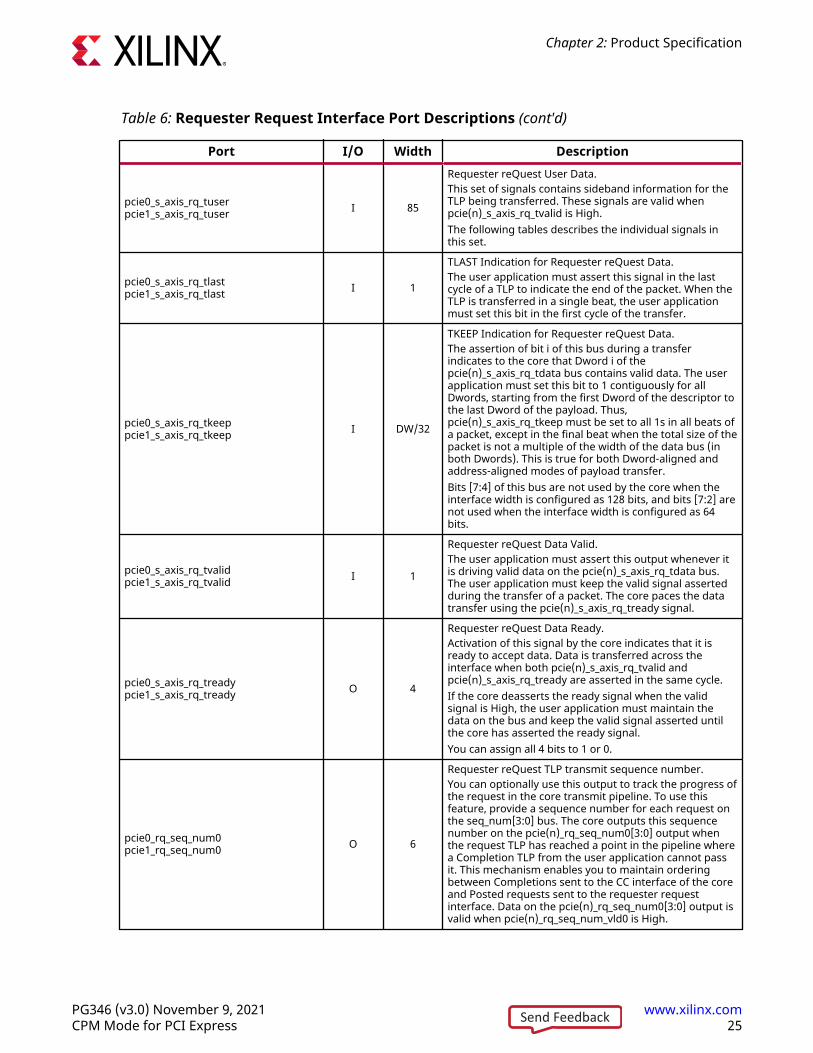
Table 6: Requester Request Interface Port Descriptions (cont'd)
Port I/O Width Description
pcie0_s_axis_rq_tuserpcie1_s_axis_rq_tuser I 85
Requester reQuest User Data.This set of signals contains sideband information for theTLP being transferred. These signals are valid whenpcie(n)_s_axis_rq_tvalid is High.The following tables describes the individual signals inthis set.
pcie0_s_axis_rq_tlastpcie1_s_axis_rq_tlast I 1
TLAST Indication for Requester reQuest Data.The user application must assert this signal in the lastcycle of a TLP to indicate the end of the packet. When theTLP is transferred in a single beat, the user applicationmust set this bit in the first cycle of the transfer.
pcie0_s_axis_rq_tkeeppcie1_s_axis_rq_tkeep I DW/32
TKEEP Indication for Requester reQuest Data.The assertion of bit i of this bus during a transferindicates to the core that Dword i of thepcie(n)_s_axis_rq_tdata bus contains valid data. The userapplication must set this bit to 1 contiguously for allDwords, starting from the first Dword of the descriptor tothe last Dword of the payload. Thus,pcie(n)_s_axis_rq_tkeep must be set to all 1s in all beats ofa packet, except in the final beat when the total size of thepacket is not a multiple of the width of the data bus (inboth Dwords). This is true for both Dword-aligned andaddress-aligned modes of payload transfer.Bits [7:4] of this bus are not used by the core when theinterface width is configured as 128 bits, and bits [7:2] arenot used when the interface width is configured as 64bits.
pcie0_s_axis_rq_tvalidpcie1_s_axis_rq_tvalid I 1
Requester reQuest Data Valid.The user application must assert this output whenever itis driving valid data on the pcie(n)_s_axis_rq_tdata bus.The user application must keep the valid signal assertedduring the transfer of a packet. The core paces the datatransfer using the pcie(n)_s_axis_rq_tready signal.
pcie0_s_axis_rq_treadypcie1_s_axis_rq_tready O 4
Requester reQuest Data Ready.Activation of this signal by the core indicates that it isready to accept data. Data is transferred across theinterface when both pcie(n)_s_axis_rq_tvalid andpcie(n)_s_axis_rq_tready are asserted in the same cycle.If the core deasserts the ready signal when the validsignal is High, the user application must maintain thedata on the bus and keep the valid signal asserted untilthe core has asserted the ready signal.You can assign all 4 bits to 1 or 0.
pcie0_rq_seq_num0pcie1_rq_seq_num0 O 6
Requester reQuest TLP transmit sequence number.You can optionally use this output to track the progress ofthe request in the core transmit pipeline. To use thisfeature, provide a sequence number for each request onthe seq_num[3:0] bus. The core outputs this sequencenumber on the pcie(n)_rq_seq_num0[3:0] output whenthe request TLP has reached a point in the pipeline wherea Completion TLP from the user application cannot passit. This mechanism enables you to maintain orderingbetween Completions sent to the CC interface of the coreand Posted requests sent to the requester requestinterface. Data on the pcie(n)_rq_seq_num0[3:0] output isvalid when pcie(n)_rq_seq_num_vld0 is High.
Chapter 2: Product Specification
PG346 (v3.0) November 9, 2021 www.xilinx.comCPM Mode for PCI Express 25Send Feedback

Table 6: Requester Request Interface Port Descriptions (cont'd)
Port I/O Width Description
pcie0_rq_seq_num_vld0pcie1_rq_seq_num_vld0 O 1
Requester reQuest TLP transmit sequence number valid.This output is asserted by the core for one cycle when ithas placed valid data on pcie(n)_rq_seq_num0[3:0].
pcie0_rq_tag0pcie0_rq_tag1pcie1_rq_tag0pcie1_rq_tag1
O 8
Requester reQuest Non-Posted tag.When tag management for Non-Posted requests isperformed by the core (AXISTEN_IF_ENABLE_CLIENT_TAGis 0), this output is used by the core to communicate theallocated tag for each Non-Posted request received.The tag value on this bus is valid for one cycle whenpcie(n)_rq_tag_vld0 is High. You must copy this tag anduse it to associate the completion data with the pendingrequest.There can be a delay of several cycles between thetransfer of the request on the pcie(n)_s_axis_rq_tdata busand the assertion of pcie(n)_rq_tag_vld0 by the core toprovide the allocated tag for the request. Meanwhile, theuser application can continue to send new requests. Thetags for requests are communicated on this bus in FIFOorder, so the user application can easily associate the tagvalue with the request it transferred.
pcie0_rq_tag_vld0pcie0_rq_tag_vld1pcie1_rq_tag_vld0pcie1_rq_tag_vld1
O 1
Requester reQuest Non-Posted tag valid.The core asserts this output for one cycle when it hasallocated a tag to an incoming Non-Posted request fromthe requester request interface and placed it on thepcie(n)_rq_tag0 output.
When PASID_CAP_ON is enabled then pcie(n)_s_axis_rq_tuser [84:62] pins areshared with cfg* ports. The following table provides more information.
Table 7: Sideband Signal Descriptions in pcie(n)_s_axis_rq_tuser
Bit Index Name Width Description
3:0 first_be[3:0] 4
Byte enables for the first Dword.This field must be set based on the desired value of theFirst_BE bits in the Transaction-Layer header of the requestTLP. For Memory Reads,I/O Reads, and Configuration Reads, these four bits indicatethe valid bytes to be read in the first Dword. For MemoryWrites, I/O Writes, and Configuration Writes, these bitsindicate the valid bytes in the first Dword of the payload.The core samples this field in the first beat of a packet,when pcie(n)_s_axis_rq_tvalid and pcie(n)_s_axis_rq_treadyare both High.
7:4 last_be[3:0] 4
Byte enables for the last Dword.This field must be set based on the desired value of theLast_BE bits in the Transaction-Layer header of the TLP. ForMemory Reads of two Dwords or more, these four bitsindicate the valid bytes to be read in the last Dword of theblock of data. For Memory Reads and Writes of one DWtransfers and zero length transfers, these bits should be 0s.For Memory Writes of two Dwords or more, these bitsindicate the valid bytes in the last Dword of the payload.The core samples this field in the first beat of a packet,when pcie(n)_s_axis_rq_tvalid and pcie(n)_s_axis_rq_treadyare both High.
Chapter 2: Product Specification
PG346 (v3.0) November 9, 2021 www.xilinx.comCPM Mode for PCI Express 26Send Feedback

Table 7: Sideband Signal Descriptions in pcie(n)_s_axis_rq_tuser (cont'd)
Bit Index Name Width Description
10:8 addr_offset[2:0] 3
When the address-aligned mode is in use on this interface,the user application must provide the byte lane numberwhere the payload data begins on the data bus, modulo 4,on this sideband bus. This enables the core to determinethe alignment of the data block being transferred.The core samples this field in the first beat of a packet,when pcie(n)_s_axis_rq_tvalid and pcie(n)_s_axis_rq_treadyare both High.When the requester request interface is configured in theDword-alignment mode, this field must always be set to 0.In Root Port configuration, Configuration Packets mustalways be aligned to DW0, and therefore for this type ofpackets, this field must be set to 0 in both alignment modes.
11 discontinue 1
This signal can be asserted by the user application during atransfer if it has detected an error in the data beingtransferred and needs to abort the packet. The core nullifiesthe corresponding TLP on the link to avoid data corruption.You can assert this signal in any cycle during the transfer.You can either choose to terminate the packet prematurelyin the cycle where the error was signaled, or continue untilall bytes of the payload are delivered to the core. In thelatter case, the core treats the error as sticky for thefollowing beats of the packet, even if the user applicationdeasserts the discontinue signal before the end of thepacket.The discontinue signal can be asserted only whenpcie(n)_s_axis_rq_tvalid is High. The core samples this signalonly when pcie(n)_s_axis_rq_tready is High. Thus, whenasserted, it should not be deasserted untilpcie(n)_s_axis_rq_tready is High. Discontinue is notsupported for Non-Posted TLPs. The user logic can assertthis signal in any cycle except the first cycle during thetransfer.When the core is configured as an Endpoint, this error isalso reported by the core to the Root Complex to which it isattached, using Advanced Error Reporting (AER).
27:24 seq_num[3:0] 4
You can optionally supply a 4-bit sequence number in thisfield to keep track of the progress of the request in the coretransmit pipeline. The core outputs this sequence numberon its pcie_rq_seq_num[3:0] output when the request TLPhas progressed to a point in the pipeline where aCompletion TLP is not able to pass it.The core samples this field in the first beat of a packet,when pcie(n)_s_axis_rq_tvalid and pcie(n)_s_axis_rq_treadyare both High.This input can be hardwired to 0 when the user applicationis not monitoring the pcie_rq_seq_num[3:0] output of thecore.
Chapter 2: Product Specification
PG346 (v3.0) November 9, 2021 www.xilinx.comCPM Mode for PCI Express 27Send Feedback

Table 7: Sideband Signal Descriptions in pcie(n)_s_axis_rq_tuser (cont'd)
Bit Index Name Width Description
59:28 parity 32
Odd parity for the 256-bit data.When parity checking is enabled in the core, the user logicmust set bit i of this bus to the odd parity computed for bytei of pcie(n)_s_axis_rq_tdata. Only the lower 16 bits are usedwhen the interface width is 128 bits, and only the lower 8bits are used when the interface width is 64 bits.When an interface parity error is detected, it is recorded asan uncorrectable internal error and the packet is discarded.According to the Base Spec 6.2.9 (PCI-SIG Specifications(https://www.pcisig.com/specifications)), an uncorrectableinternal error is an error that occurs within a componentthat results in improper operation of the component. Theonly method of recovering from an uncorrectable internalerror is a reset or hardware replacement.The parity bits can be permanently tied to 0 if parity check isnot enabled in the core.
61:60 seq_num[5:4] 2 Extension of seq_num as in [27:24].
62 PASID TLP Valid 1 Indicates PASID TLP is valid.
82:63 PASID 20 Indicates PASID TLP prefix.
83 Execute Requested 1 Indicates Execute Requested.
84 Privileged Mode Requested 1 Indicates Privileged Mode Requested.
Requester Completion Interface
The Requester Completion (RC) interface are the ports through which the completions receivedfrom the link in response to your requests are presented to the user application. The followingtable defines the ports in the RC interface of the core. In the Width column, DW denotes theconfigured data bus width (64, 128, or 256 bits).
Table 8: Requester Completion Interface Port Descriptions
Port I/O Width Description
pcie0_m_axis_rc_tdatapcie1_m_axis_rc_tdata O DW
Requester Completion Data bus.Transmit data from the core requester completion interfaceto the user application. Only the lower 128 bits are usedwhen the interface width is 128 bits, and only the lower 64bits are used when the interface width is 64 bits.Bits [255:128] are set permanently to 0 by the core when theinterface width is configured as 128 bits, and bits [255:64]are set permanently to 0 when the interface width isconfigured as 64 bits.
pcie0_m_axis_rc_tuserpcie1_m_axis_rc_tuser O 75
Requester Completion User Data.This set of signals contains sideband information for the TLPbeing transferred. These signals are valid whenpcie(n)_m_axis_rc_tvalid is High.The following table describes the individual signals in thisset.
Chapter 2: Product Specification
PG346 (v3.0) November 9, 2021 www.xilinx.comCPM Mode for PCI Express 28Send Feedback

Table 8: Requester Completion Interface Port Descriptions (cont'd)
Port I/O Width Description
pcie0_m_axis_rc_tlastpcie1_m_axis_rc_tlast O 1
TLAST indication for Requester Completion Data.The core asserts this signal in the last beat of a packet toindicate the end of the packet. When a TLP is transferred ina single beat, the core sets this bit in the first beat of thetransfer. This output is used only when the straddle optionis disabled. When the straddle option is enabled (for the256-bit interface), the core sets this output permanently to0.
pcie0_m_axis_rc_tkeeppcie1_m_axis_rc_tkeep O DW/32
TKEEP indication for Requester Completion Data.The assertion of bit i of this bus during a transfer indicatesthat Dword i of the pcie(n)_m_axis_rc_tdata bus containsvalid data. The core sets this bit to 1 contiguously for allDwords starting from the first Dword of the descriptor tothe last Dword of the payload. Thus, pcie(n)_m_axis_rc_tkeepsets to 1s in all beats of a packet, except in the final beatwhen the total size of the packet is not a multiple of thewidth of the data bus (both in Dwords). This is true for bothDword-aligned and address-aligned modes of payloadtransfer.Bits [7:4] of this bus are set permanently to 0 by the corewhen the interface width is configured as 128 bits, and bits[7:2] are set permanently to 0 when the interface width isconfigured as 64 bits.These outputs are permanently set to all 1s when theinterface width is 256 bits and the straddle option isenabled. The user logic must use the signals inpcie(n)_m_axis_rc_tuser in that case to determine thestart and end of Completion TLPs transferred over theinterface.
pcie0_m_axis_rc_tvalidpcie1_m_axis_rc_tvalid O 1
Requester Completion Data Valid.The core asserts this output whenever it is driving valid dataon the pcie(n)_m_axis_rc_tdata bus. The core keeps the validsignal asserted during the transfer of a packet. The userapplication can pace the data transfer using thepcie(n)_m_axis_rc_tready signal.
pcie0_m_axis_rc_treadypcie1_m_axis_rc_tready I 1
Requester Completion Data Ready.Activation of this signal by the user logic indicates to thecore that the user application is ready to accept data. Data istransferred across the interface when bothpcie(n)_m_axis_rc_tvalid and pcie(n)_m_axis_rc_tready areasserted in the same cycle.If the user application deasserts the ready signal when thevalid signal is High, the core maintains the data on the busand keeps the valid signal asserted until the user applicationhas asserted the ready signal.
Chapter 2: Product Specification
PG346 (v3.0) November 9, 2021 www.xilinx.comCPM Mode for PCI Express 29Send Feedback

Table 9: Sideband Signal Descriptions in pcie(n)_m_axis_rc_tuser
Bit Index Name Width Description
31:0 byte_en 32
The user logic can optionally use these byte enable bits todetermine the valid bytes in the payload of a packet beingtransferred. The assertion of bit i of this bus during atransfer indicates that byte i of the pcie(n)_m_axis_rc_tdatabus contains a valid payload byte. This bit is not asserted fordescriptor bytes.Although the byte enables can be generated by user logicfrom information in the request descriptor (address andlength), the logic has the option to use these signals directlyinstead of generating them from other interface signals.The 1 bit in this bus for the payload of a TLP is alwayscontiguous.Bits [31:16] of this bus are set permanently to 0 by the corewhen the interface width is configured as 128 bits, and bits[31:8] are set permanently to 0 when the interface width isconfigured as 64 bits. The byte enable bit is also set oncompletions received in response to zero length memoryread requests.
32 is_sof_0 1
Start of a first Completion TLP.For 64-bit and 128-bit interfaces, and for the 256-bitinterface with no straddling, is_sof_0 is asserted by the corein the first beat of a packet to indicate the start of the TLP.On these interfaces, only a single TLP can be started in adata beat, and is_sof_1 is permanently set to 0. Use of thissignal is optional when the straddle option is not enabled.When the interface width is 256 bits and the straddle optionis enabled, the core can straddle two Completion TLPs in thesame beat. In this case, the Completion TLPs are notformatted as AXI4-Stream packets. The assertion of is_sof_0indicates a Completion TLP starting in the beat. The firstbyte of this Completion TLP is in byte lane 0 if the previousTLP ended before this beat, or in byte lane 16 if the previousTLP continues in this beat.
33 is_sof_1 1
This signal is used when the interface width is 256 bits andthe straddle option is enabled, when the core can straddletwo Completion TLPs in the same beat. The output ispermanently set to 0 in all other cases.The assertion of is_sof_1 indicates a second Completion TLPstarting in the beat, with its first bye in byte lane 16. Thecore starts a second TLP at byte position 16 only if theprevious TLP ended in one of the byte positions 0-15 in thesame beat; that is, only if is_eof_0[0] is also set in the samebeat.
37:34 is_eof_0[3:0] 4
End of a first Completion TLP and the offset of its lastDword.These outputs are used only when the interface width is 256bits and the straddle option is enabled.The assertion of the bit is_eof_0[0] indicates the end of afirst Completion TLP in the current beat. When this bit is set,the bits is_eof_0[3:1] provide the offset of the last Dword ofthis TLP.
Chapter 2: Product Specification
PG346 (v3.0) November 9, 2021 www.xilinx.comCPM Mode for PCI Express 30Send Feedback

Table 9: Sideband Signal Descriptions in pcie(n)_m_axis_rc_tuser (cont'd)
Bit Index Name Width Description
41:38 is_eof_1[3:0] 4
End of a second Completion TLP and the offset of its lastDword.These outputs are used only when the interface width is 256bits and the straddle option is enabled. The core can thenstraddle two Completion TLPs in the same beat. Theseoutputs are reserved in all other cases.The assertion of is_eof_1[0] indicates a second TLP ending inthe same beat. When bit 0 of is_eof_1 is set, bits [3:1]provide the offset of the last Dword of the TLP ending in thisbeat. Because the second TLP can only end at a byteposition in the range 27–31, is_eof_1[3:1] can only take oneof two values (6 or 7).The offset for the last byte of the second TLP can bedetermined from the starting address and length of the TLP,or from the byte enable signals byte_en[31:0].If is_eof_1[0] is High, the signals is_eof_0[0] and is_sof_1are also High in the same beat.
42 discontinue 1
This signal is asserted by the core in the last beat of a TLP, ifit has detected an uncorrectable error while reading the TLPpayload from its internal FIFO memory. The user applicationmust discard the entire TLP when such an error is signaledby the core.This signal is never asserted when the TLP has no payload.It is asserted only in the last beat of the payload transfer;that is, when is_eof_0[0] is High.When the straddle option is enabled, the core does not starta second TLP if it has asserted discontinue in a beat.When the core is configured as an Endpoint, the error is alsoreported by the core to the Root Complex to which it isattached, using Advanced Error Reporting (AER).
74:43 parity 32
Odd parity for the 256-bit transmit data.Bit i provides the odd parity computed for byte i ofpcie(n)_m_axis_rc_tdata. Only the lower 16 bits are usedwhen the interface width is 128 bits, and only the lower 8bits are used when the interface width is 64 bits. Bits [31:16]are set permanently to 0 by the core when the interfacewidth is configured as 128 bits, and bits [31:8] are setpermanently to 0 when the interface width is configured as64 bits.
512-bit Interfaces
This section provides the description for ports associated with the user interfaces of the core.
Completer Request Interface
Table 10: Completer Request Interface Port Descriptions (512-bit Interface)
Name I/O Width Descriptionpcie0_m_axis_cq_tdatapcie1_m_axis_cq_tdata O 512 Transmit data from the PCIe completer request interface
to the user application.
Chapter 2: Product Specification
PG346 (v3.0) November 9, 2021 www.xilinx.comCPM Mode for PCI Express 31Send Feedback

Table 10: Completer Request Interface Port Descriptions (512-bit Interface) (cont'd)
Name I/O Width Description
pcie0_m_axis_cq_tuserpcie1_m_axis_cq_tuser O 229
This is a set of signals containing sideband informationfor the TLP being transferred. These signals are validwhen pcie(n)_m_axis_cq_tvalid is High. The individualsignals in this set are described in the following table.
pcie0_m_axis_cq_tlastpcie1_m_axis_cq_tlast O 1
The core asserts this signal in the last beat of a packet toindicate the end of the packet. When a TLP is transferredin a single beat, the core sets this bit in the first beat ofthe transfer. This output is used only when the straddleoption is disabled. When the straddle option is enabled,the core sets this output permanently to 0.
pcie0_m_axis_cq_tkeeppcie1_m_axis_cq_tkeep O 16
The assertion of bit i of this bus during a transferindicates to the user logic that Dword i of thepcie(n)_m_axis_cq_tdata bus contains valid data. The coresets this bit to 1 contiguously for all Dwords starting fromthe first Dword of the descriptor to the last Dword of thepayload. Thus, pcie(n)_m_axis_cq_tdata is set to all 1s in allbeats of a packet, except in the final beat when the totalsize of the packet is not a multiple of the width of the databus (both in Dwords). This is true for both Dword-alignedand 128b address-aligned modes of payload transfer.The tkeep bits are valid only when straddle is not enabledon the CQ interface. When straddle is enabled, the tkeepbits are permanently set to all 1s in all beats. The userlogic must use the is_sop/is_eop signals in thepcie(n)_m_axis_cq_tuser bus in that case to determine thestart and end of TLPs transferred over the interface.
pcie0_m_axis_cq_tvalidpcie1_m_axis_cq_tvalid O 1
The core asserts this output whenever it is driving validdata on the pcie(n)_m_axis_cq_tdata bus. The core keepsthe valid signal asserted during the transfer of a packet.The user application can pace the data transfer using thepcie(n)_m_axis_cq_tready signal.
pcie0_m_axis_cq_treadypcie1_m_axis_cq_tready I 1
Activation of this signal by the user logic indicates to thePCIe core that the user logic is ready to accept data. Datais transferred across the interface when bothpcie(n)_m_axis_cq_tvalid and pcie(n)_m_axis_cq_tready areasserted in the same cycle.If the user logic deasserts the ready signal whenpcie(n)_m_axis_cq_tvalid is High, the core maintains thedata on the bus and keeps the valid signal asserted untilthe user logic has asserted the ready signal.
Chapter 2: Product Specification
PG346 (v3.0) November 9, 2021 www.xilinx.comCPM Mode for PCI Express 32Send Feedback

Table 10: Completer Request Interface Port Descriptions (512-bit Interface) (cont'd)
Name I/O Width Description
pcie0_cq_np_reqpcie1_cq_np_req I 2
This input is used by the user application to request thedelivery of a Non-Posted request. The core implements acredit-based flow control mechanism to control thedelivery of Non-Posted requests across the interface,without blocking Posted TLPs.This input to the core controls an internal credit count.The credit count is updated in each clock cycle based onthe setting of pcie_cq_np_req[1:0] as follows:• 00: No change• 01: Increment by 1• 10 or 11: Increment by 2The credit count is decremented on the delivery of eachNon-Posted request across the interface. The coretemporarily stops delivering Non-Posted requests to theuser logic when the credit count is zero. It continues todeliver any Posted TLPs received from the link even whenthe delivery of Non-Posted requests has been paused.The user application can either set pcie_cq_np_req[1:0] ineach cycle based on the status of its Non-Posted requestreceive buffer, or can set it to 11 permanently if it doesnot need to exercise selective backpressure on Non-Posted requests.The setting of pcie_cq_np_req[1:0] does not need to bealigned with the packet transfers on the completerrequest interface.
pcie0_cq_np_req_countpcie1_cq_np_req_count O 6
This output provides the current value of the credit countmaintained by the core for delivery of Non-Postedrequests to the user logic. The core delivers a Non-Postedrequest across the completer request interface only whenthis credit count is non-zero. This counter saturates at amaximum limit of 32.Because of internal pipeline delays, there can be severalcycles of delay between the user application providingcredit on the pcie_cq_np_req[1:0] inputs and the PCIe coreupdating the pcie_cq_np_req_count output in response.This count resets on user_reset and de-assertion ofuser_lnk_up.
When PASID_CAP_ON is enabled then pcie(n)_m_axis_cq_tuser[228:183] pins areshared with cfg* ports. The following table provides more information.
Chapter 2: Product Specification
PG346 (v3.0) November 9, 2021 www.xilinx.comCPM Mode for PCI Express 33Send Feedback

Table 11: Sideband Signals in pcie(n)_m_axis_cq_tuser (512-bit Interface)
Bit Index Name Width Description
7:0 first_be[7:0] 8
Byte enables for the first Dword of the payload. first_be[3:0]reflects the setting of the First Byte Enable bits in theTransaction-Layer header of the first TLP in this beat; andfirst_be[7:4] reflects the setting of the First Byte Enable bitsin the Transaction-Layer header of the second TLP in thisbeat. For Memory Reads and I/O Reads, the 4 bits indicatethe valid bytes to be read in the first Dword. For MemoryWrites and I/O Writes, these bits indicate the valid bytes inthe first Dword of the payload. For Atomic Operations andMessages with a payload, these bits are set to all 1s.Bits [7:4] of first_be are valid only when straddle is enabledon the CQ interface. When straddle is disabled, these bitsare permanently set to 0s.This field is valid in the first beat of a packet. first_be[3:0] isvalid when pcie(n)_m_axis_cq_tvalid and is_sop[0] are bothasserted High. first_be[7:4] is valid whenpcie(n)_m_axis_cq_tvalid and is_sop[1] are both assertedHigh.
15:8 last_be[7:0] 8
Byte enables for the last Dword of the payload. last_be[3:0]reflects the setting of the Last Byte Enable bits in theTransaction-Layer header of the first TLP in this beat; andlast_be[7:4] reflects the setting of the Last Byte Enable bitsin the Transaction-Layer header of the second TLP in thisbeat. For Memory Reads, the 4 bits indicate the valid bytesto be read in the last Dword of the block of data. ForMemory Writes, these bits indicate the valid bytes in theending Dword of the payload. For Memory Reads and Writesof one DW transfers and zero length transfers, these bitsshould be 0s. For Atomic Operations and Messages with apayload, these bits are set to all 1s.Bits [7:4] of last_be are valid only when straddle is enabledon the CQ interface. When straddle is disabled, these bitsare permanently set to 0s.This field is valid in the first beat of a packet. last_be[3:0] isvalid when pcie(n)_m_axis_cq_tvalid and is_eop[0] are bothasserted High. last_be[7:4] is valid whenpcie(n)_m_axis_cq_tvalid and is_eop[1] are both assertedHigh.
79:16 byte_en[63:0] 64
The user logic can optionally use these byte enable bits todetermine the valid bytes in the payload of a packet beingtransferred The assertion of bit i of this bus during atransfer indicates to the user logic that byte i of thepcie(n)_m_axis_cq_tdata bus contains a valid payload byte.This bit is not asserted for descriptor bytes.Although the byte enables can be generated by user logicfrom information in the request descriptor (address andlength), as well as the settings of the first_be and last_besignals, the user logic has the option of using these signalsdirectly instead of generating them from other interfacesignals.When the payload size is more than 2 Dwords (8 bytes), thefirst bits on this bus for the payload are always contiguous.When the payload size is 2 Dwords or less, the first bitsmight be non-contiguous.For the special case of a zero-length memory writetransaction defined by the PCI ExpressSpecifications, thebyte_en bits are all 0 when the associated 1 Dword payloadis being transferred.
Chapter 2: Product Specification
PG346 (v3.0) November 9, 2021 www.xilinx.comCPM Mode for PCI Express 34Send Feedback

Table 11: Sideband Signals in pcie(n)_m_axis_cq_tuser (512-bit Interface) (cont'd)
Bit Index Name Width Description
81:80 is_sop[1:0] 2
Signals the start of a new TLP in this beat. These outputs areset in the first beat of a TLP. When straddle is disabled, onlyis_sop[0] is valid and is_sop[1] is permanently set to 0. Whenstraddle is enabled, the settings are as follows:• 00: No new TLP starting in this beat.• 01: A single new TLP starts in this beat. Its start position
is indicated by is_sop0_ptr[1:0].• 11: Two new TLPs are starting in this beat.
is_sop0_ptr[1:0] provides the start position of the firstTLP and is_sop1_ptr[1:0] provides the start position ofthe second TLP.
• 10: Reserved.Use of this signal is optional for the user logic when thestraddle option is disabled, because a new TLP always startsin the beat following tlast assertion.
83:82 is_sop0_ptr[1:0] 2
Indicates the position of the first byte of the first TLPstarting in this beat:• 00: Byte lane 0• 10: Byte lane 32• 01, 11: ReservedThis field is valid only when the straddle option is enabledon the CQ interface. Otherwise, it is set to 0 permanently, asa TLP can only start in bye lane 0.
85:84 is_sop1_ptr[1:0] 2
Indicates the position of the first byte of the second TLPstarting in this beat:• 10: Byte lane 32• 00, 01, 11: Reserved.This output is used only when the straddle option is enabledon the CQ interface. The core can then straddle two TLPs inthe same beat. The output is permanently set to 0 whenstraddle is disabled.
87:86 is_eop[1:0] 2
Indicates that a TLP is ending in this beat. These outputs areset in the final beat of a TLP. When straddle is disabled, onlyis_eop[0] is valid and is_eop[1] is permanently set to 0.When straddle is enabled, the settings are as follows:• 00: No TLPs ending in this beat.• 01: A single TLP is ending in this beat. is_eop0_ptr[3:0]
provides the offset of the last Dword of this TLP.• 11: Two TLPs are ending in this beat. is_eop0_ptr[3:0]
provides the offset of the last Dword of the first TLP andis_eop1_ptr[3:0]provides the offset of the last Dword ofthe second TLP.
• 10: Reserved.The use of this signal is optional for the user logic when thestraddle option is not enabled, because tlast Is asserted inthe final beat of a TLP.
91:88 is_eop0_ptr[3:0] 4 Offset of the last Dword of the first TLP ending in this beat.This output is valid when is_eop[0] is asserted.
95:92 is_eop1_ptr[3:0] 4
Offset of the last Dword of the second TLP ending in thisbeat. This output is valid when is_eop[1] is asserted.The output is permanently set to 0 when straddle isdisabled.
Chapter 2: Product Specification
PG346 (v3.0) November 9, 2021 www.xilinx.comCPM Mode for PCI Express 35Send Feedback

Table 11: Sideband Signals in pcie(n)_m_axis_cq_tuser (512-bit Interface) (cont'd)
Bit Index Name Width Description
96 discontinue 1
This signal is asserted by the core in the last beat of a TLP, ifit has detected an uncorrectable error while reading the TLPpayload from its internal FIFO memory. The user applicationmust discard the entire TLP when such an error is signaledby the core.This signal is never asserted when the TLP has no payload.It is asserted only in the last beat of the payload transfer,that is when is_eop[0] is High.When the straddle option is enabled, the core does not starta second TLP if it has asserted discontinue in a beat.When the core is configured as an Endpoint, the error is alsoreported by the core to the Root Complex it is attached to,using Advanced Error Reporting (AER).
182:119 parity 64 Odd parity for the 512-bit transmit data. Bit i provides theodd parity computed for byte i of pcie(n)_m_axis_cq_tdata.
183 PASID TLP Valid 0 1 Indicates PASID TLP 0 is valid.
184 PASID TLP Valid 1 1 Indicates PASID TLP 1 is valid.
204:185 PASID 0 20 Indicates PASID TLP Prefix for packet0 to the user design.
224:205 PASID 1 20 Indicates PASID TLP Prefix for packet1 to the user design.
225 Execute Requested 0 1 Indicates Execute Requested for packet0.
226 Execute Requested 1 1 Indicates Execute Requested for packet1.
227 Privileged Mode Requested 0 1 Indicates Privileged Mode Requested for packet0 to the userdesign.
228 Privileged Mode Requested 1 1 Indicates Privileged Mode Requested for packet1 to the userdesign.
Completer Completion Interface
Table 12: Completer Completion Interface Port Descriptions (512-bit Interface)
Name I/O Width Descriptionpcie0_s_axis_cc_tdatapcie1_s_axis_cc_tdata I 512 Completion data from the user application to the PCIe core.
pcie0_s_axis_cc_tuserpcie1_s_axis_cc_tuser I 81
This is a set of signals containing sideband information forthe TLP being transferred. These signals are valid whenpcie(n)_s_axis_cc_tvalid is High.The individual signals in this set are described in thefollowing table.
pcie0_s_axis_cc_tlastpcie1_s_axis_cc_tlast I 1
The user application must assert this signal in the last cycleof a packet to indicate the end of the packet. When the TLPis transferred in a single beat, the user application must setthis bit in the first cycle of the transfer.This input is used by the core only when the straddle optionis disabled. When the straddle option is enabled, the coreignores the setting of this input, using instead the is_sop/is_eop signals in the pcie(n)_s_axis_cc_tuser bus todetermine the start and end of TLPs.
Chapter 2: Product Specification
PG346 (v3.0) November 9, 2021 www.xilinx.comCPM Mode for PCI Express 36Send Feedback

Table 12: Completer Completion Interface Port Descriptions (512-bit Interface) (cont'd)
Name I/O Width Description
pcie0_s_axis_cc_tkeeppcie1_s_axis_cc_tkeep I 16
The assertion of bit i of this bus during a transfer indicatesto the core that Dword i of the pcie(n)_s_axis_cc_tdata buscontains valid data. The user logic must set this bit to 1contiguously for all Dwords starting from the first Dword ofthe descriptor to the last Dword of the payload. Thus,pcie(n)_s_axis_cc_tdata must be set to all 1s in all beats of apacket, except in the final beat when the total size of thepacket is not a multiple of the width of the data bus (both inDwords). This is true for both Dword-aligned and 128baddress-aligned modes of payload transfer.The tkeep bits are valid only when straddle is not enabledon the CC interface. When straddle is enabled, the coreignores the setting of these bits when receiving data acrossthe interface. The user logic must set the is_sop/is_eopsignals in the pcie(n)_s_axis_cc_tuser bus in that case tosignal the start and end of TLPs transferred over theinterface.
pcie0_s_axis_cc_tvalidpcie1_s_axis_cc_tvalid I 1
The user application must assert this output whenever it isdriving valid data on the pcie(n)_s_axis_cc_tdata bus. Theuser application must keep the valid signal asserted duringthe transfer of a packet. The core paces the data transferusing the pcie(n)_s_axis_cc_tready signal.
pcie0_s_axis_cc_treadypcie1_s_axis_cc_tready O 4
Activation of this signal by the PCIe core indicates that it isready to accept data. Data is transferred across the interfacewhen both pcie(n)_s_axis_cc_tvalid andpcie(n)_s_axis_cc_tready are asserted in the same cycle.If the core deasserts the ready signal when the valid signalis High, the user logic must maintain the data on the busand keep the valid signal asserted until the core hasasserted the ready signal.With this output port, each bit indicates the same value, sothe user logic can use any of the bit.
Table 13: Sideband Signals in pcie(n)_s_axis_cc_tuser
Bit Index Name Width Description
1:0 is_sop[1:0] 2
Signals the start of a new TLP in this beat. These outputs areset in the first beat of a TLP. When straddle is disabled, onlyis_sop[0] is valid. When straddle is enabled, the settings areas follows:• 00: No new TLP starting in this beat.• 01: A single new TLP starts in this beat. Its start position
is indicated by is_sop0_ptr[1:0].• 11: Two new TLPs are starting in this beat.
is_sop0_ptr[1:0] provides the start position of the firstTLP and is_sop1_ptr[1:0] provides the start position ofthe second TLP.
• 10: Reserved.This field is used by the core only when the straddle optionis enabled. When straddle is disabled, the core uses tlast todetermine the first beat of an incoming TLP.
Chapter 2: Product Specification
PG346 (v3.0) November 9, 2021 www.xilinx.comCPM Mode for PCI Express 37Send Feedback

Table 13: Sideband Signals in pcie(n)_s_axis_cc_tuser (cont'd)
Bit Index Name Width Description
3:2 is_sop0_ptr[1:0] 2
Indicates the position of the first byte of the first TLPstarting in this beat:• 00: Byte lane 0• 10: Byte lane 32• 01, 11: ReservedThis field is used by the core only when the straddle optionis enabled. When straddle is disabled, the user logic mustalways start a TLP in byte lane 0.
5:4 is_sop1_ptr[1:0] 2
Indicates the position of the first byte of the second TLPstarting in this beat:• 10: Byte lane 32• 00, 01, 11: Reserved.This input is used only when the straddle option is enabledon the CC interface. The user can then straddle two TLPs inthe same beat.
7:6 is_eop[1:0] 2
Signals that a TLP is ending in this beat. These outputs areset in the final beat of a TLP. When straddle is disabled, onlyis_eop[0] is valid. When straddle is enabled, the settings areas follows:• 00: No TLPs ending in this beat.• 01: A single TLP is ending in this beat. is_eop0_ptr[3:0]
provides the offset of the last Dword of this TLP.• 11: Two TLPs are ending in this beat. is_eop0_ptr[3:0]
provides the offset of the last Dword of the first TLP andis_eop1_ptr[3:0] provides the offset of the last Dword ofthe second TLP.
• 10: Reserved.This field is used by the core only when the straddle optionis enabled. When straddle is disabled, the core uses tlastand tkeep to determine the ending beat and position ofEOP.
11:8 is_eop0_ptr[3:0] 4
Offset of the last Dword of the first TLP ending in this beat.This output is valid when is_eop[0] is asserted.This field is used by the core only when the straddle optionis enabled.
15:12 is_eop1_ptr[3:0] 4
Offset of the last Dword of the second TLP ending in thisbeat. This output is valid when is_eop[1] is asserted.This field is used by the core only when the straddle optionis enabled.
Chapter 2: Product Specification
PG346 (v3.0) November 9, 2021 www.xilinx.comCPM Mode for PCI Express 38Send Feedback

Table 13: Sideband Signals in pcie(n)_s_axis_cc_tuser (cont'd)
Bit Index Name Width Description
16 discontinue 1
This signal can be asserted by the user application during atransfer if it has detected an error (such as an uncorrectableECC error while reading the payload from memory) in thedata being transferred and needs to abort the packet. Thecore nullifies the corresponding TLP on the link to avoiddata corruption.The user logic can assert this signal in any beat during thetransfer except the first beat of the TLP. It can either chooseto terminate the packet prematurely in the cycle where theerror was signaled, or continue until all bytes of the payloadare delivered to the core. In the latter case, the core treatsthe error as sticky for the following beats of the packet, evenif the user logic deasserts the discontinue signal before theend of the packet.The discontinue signal can be asserted only whenpcie(n)_s_axis_cc_tvalid is High. The core samples this signalonly when pcie(n)_s_axis_cc_tready is High. Thus, onceasserted, it should not be deasserted untilpcie(n)_s_axis_cc_tready is High.When the straddle option is enabled on the CC interface, theuser should not start a new TLP in the same beat when aTLP is ending with discontinue asserted.When the core is configured as an Endpoint, this error isalso reported by the core to the Root Complex it is attachedto, using Advanced Error Reporting (AER).
80:17 parity 64
Odd parity for the 256-bit data. When parity checking isenabled in the core, user logic must set bit i of this bus tothe odd parity computed for byte i ofpcie(n)_s_axis_cc_tdata.On detection of a parity error, the core nullifies thecorresponding TLP on the link and reports it as anUncorrectable Internal Error.The parity bits can be permanently tied to 0 if parity check isnot enabled in the core.
Requester Request Interface
Table 14: Requester Request Interface Port Descriptions (512-bit Interface)
Name Width I/O Descriptionpcie0_s_axis_rq_tdatapcie1_s_axis_rq_tdata 512 I Requester-side request data from the user application to
the PCIe core.
pcie0_s_axis_rq_tuserpcie1_s_axis_rq_tuser 183 I
This is a set of signals containing sideband information forthe TLP being transferred. These signals are valid whenpcie(n)_s_axis_rq_tvalid is High. The individual signals in thisset are described in the following table.
pcie0_s_axis_rq_tlastpcie1_s_axis_rq_tlast 1 I
The user application must assert this signal in the last cycleof a TLP to indicate the end of the packet. When the TLP istransferred in a single beat, the user logic must set this bitin the first cycle of the transfer.This input is used by the core only when the straddle optionis disabled. When the straddle option is enabled, the coreignores the setting of this input, using instead the is_sop/is_eop signals in the s_axis_rq_tuser bus to determine thestart and end of TLPs.
Chapter 2: Product Specification
PG346 (v3.0) November 9, 2021 www.xilinx.comCPM Mode for PCI Express 39Send Feedback

Table 14: Requester Request Interface Port Descriptions (512-bit Interface) (cont'd)
Name Width I/O Description
pcie0_s_axis_rq_tkeeppcie1_s_axis_rq_tkeep 16 I
The assertion of bit i of this bus during a transfer indicatesto the core that Dword i of the pcie(n)_s_axis_rq_tdata buscontains valid data. The user logic must set this bit to 1contiguously for all Dwords starting from the first Dword ofthe descriptor to the last Dword of the payload. Thus,pcie(n)_s_axis_rq_tdata must be set to all 1s in all beats of apacket, except in the final beat when the total size of thepacket is not a multiple of the width of the data bus (both inDwords). This is true for both Dword-aligned and 128baddress-aligned modes of payload transfer.The tkeep bits are valid only when straddle is not enabledon the RQ interface. When straddle is enabled, the coreignores the setting of these bits when receiving data acrossthe interface. The user logic must set the is_sop/is_eopsignals in the pcie(n)_s_axis_rq_tuser bus in that case tosignal the start and end of TLPs transferred over theinterface.
pcie0_s_axis_rq_tvalidpcie1_s_axis_rq_tvalid 1 I
The user application must assert this output whenever it isdriving valid data on the pcie(n)_s_axis_rq_tdata bus. Theuser application must keep the valid signal asserted duringthe transfer of a packet. The core paces the data transferusing the pcie(n)_s_axis_rq_tready signal.
pcie0_s_axis_rq_treadypcie1_s_axis_rq_tready 4 O
Activation of this signal by the PCIe core indicates that it isready to accept data. Data is transferred across the interfacewhen both pcie(n)_s_axis_rq_tvalid andpcie(n)_s_axis_rq_tready are asserted in the same cycle.If the core deasserts the ready signal when the valid signalis High, the user logic must maintain the data on the busand keep the valid signal asserted until the core hasasserted the ready signal.With this output port, each bit indicates the same value, sothe user logic can use any of the bit.
pcie0_rq_tag_vld0pcie1_rq_tag_vld0 1 O
The core asserts this output for one cycle when it hasallocated a tag to an incoming Non-Posted request from therequester request interface and placed it on thepcie(n)_rq_tag0 output. The bit is encoded as follows:• 0: No tags being provided in this cycle.• 1: A tag is presented on pcie(n)_rq_tag0.
pcie0_rq_tag_vld1pcie1_rq_tag_vld1 1 O
The core asserts this output for one cycle when it hasallocated a tag to an incoming Non-Posted request from therequester request interface and placed it on thepcie(n)_rq_tag1 output. The bit is encoded as follows:• 0: No tag is provided on pcie(n)_rq_tag1 in this cycle.• 1: A tag is presented on pcie(n)_rq_tag1.
Chapter 2: Product Specification
PG346 (v3.0) November 9, 2021 www.xilinx.comCPM Mode for PCI Express 40Send Feedback

Table 14: Requester Request Interface Port Descriptions (512-bit Interface) (cont'd)
Name Width I/O Description
pcie0_rq_tag0pcie1_rq_tag0 8 O
When tag management for Non-Posted requests isperformed by the core (Enable Client Tag is unchecked inthe IP customization GUI), this output is used by the core tocommunicate the allocated tag for each Non-Posted requestreceived from the client. The tag value on pcie(n)_rq_tag0 isvalid for one cycle when pcie(n)_rq_tag_vld0 is High. Theclient must copy this tag and use it to associate thecompletion data with the pending request.There can be a delay of several cycles between the transferof the request on the pcie(n)_s_axis_rq_tdata bus and theassertion of pcie(n)_rq_tag_vld0 by the core to provide theallocated tag for the request. The client can, meanwhile,continue to send new requests. The tags for requests arecommunicated on this bus in FIFO order. Therefore, theuser application must associate the allocated tags with therequests in the order in which the requests were transferredover the interface.When pcie(n)_rq_tag0 and pcie(n)_rq_tag1 are both valid inthe same cycle, the value on pcie(n)_rq_tag0 corresponds tothe earlier of the two requests transferred over theinterface.
pcie0_rq_tag1pcie1_rq_tag1 8 O
The description of this signal is the same as pcie(n)_rq_tag0,except the tag value on pcie(n)_rq_tag1 is valid for one cyclewhen pcie(n)_rq_tag_vld1 is asserted.
pcie0_rq_seq_num0pcie1_rq_seq_num0 6 O
The user may optionally use this output to keep track of theprogress of the request in the core's transmit pipeline. Touse this feature, the user application must provide asequence number for each request on thepcie(n)_s_axis_rq_seq_num0[5:0] bus. The core outputs thissequence number on the pcie(n)_rq_seq_num0[5:0] outputwhen the request TLP has progressed to a point in thepipeline where a Completion TLP from the client will not beable to pass it. This mechanism enables the client tomaintain ordering between Completions sent to thecompleter completion interface of the core and Postedrequests sent to the requester request interface.Data on the pcie(n)_rq_seq_num0[5:0] output is valid whenpcie(n)_rq_seq_num_ vld0 is High.
pcie0_rq_seq_num1pcie1_rq_seq_num1 6 O
This output is identical in function to that ofpcie(n)_rq_seq_num0. It is used to provide a secondsequence number in the same cycle when a first sequencenumber is being presented on pcie(n)_rq_seq_num0.Data on the pcie(n)_rq_seq_num1[5:0] output is valid whenpcie(n)_rq_seq_num_ vld1 is High.
pcie0_rq_seq_num_vld0pcie1_rq_seq_num_vld0 1 O This output is asserted by the core for one cycle when it has
placed valid data on pcie(n)_rq_seq_num0[5:0].
pcie0_rq_seq_num_vld1pcie1_rq_seq_num_vld1 1 O This output is asserted by the core for one cycle when it has
placed valid data on pcie(n)_rq_seq_num1[5:0].
When PASID_CAP_ON is enabled then pcie(n)_s_axis_rq_tuser [182:137] pins areshared with cfg* ports. The following tables provides more details.
Chapter 2: Product Specification
PG346 (v3.0) November 9, 2021 www.xilinx.comCPM Mode for PCI Express 41Send Feedback
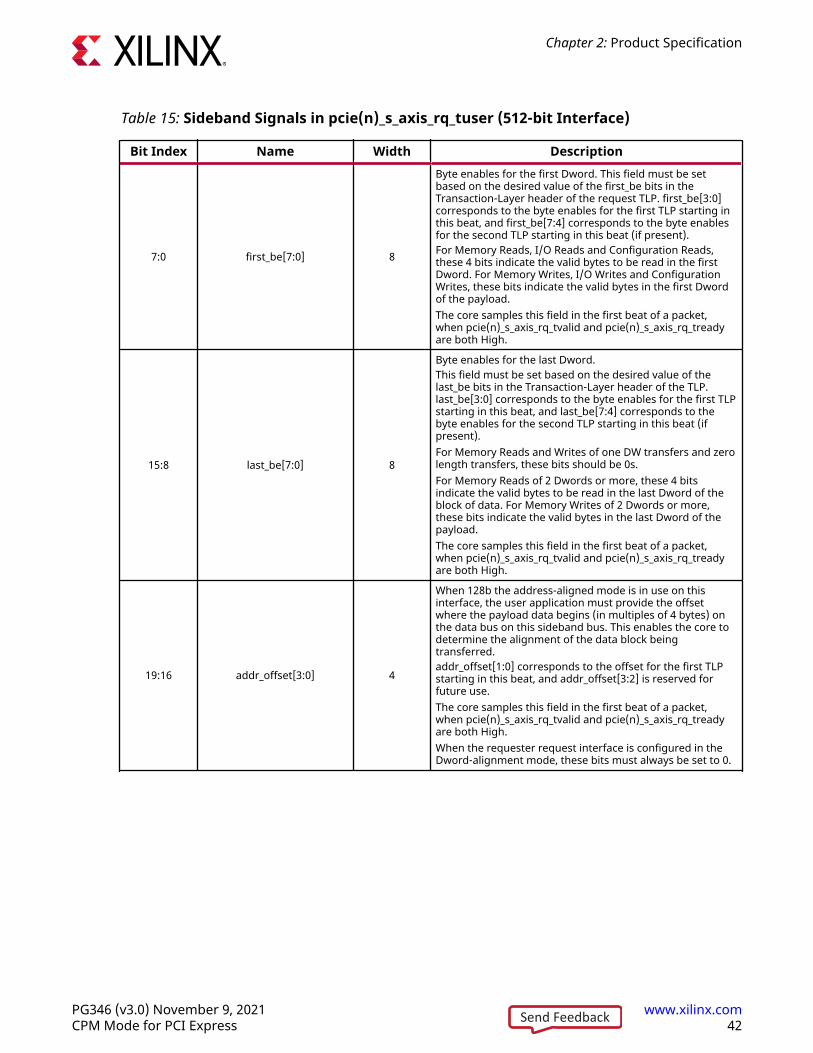
Table 15: Sideband Signals in pcie(n)_s_axis_rq_tuser (512-bit Interface)
Bit Index Name Width Description
7:0 first_be[7:0] 8
Byte enables for the first Dword. This field must be setbased on the desired value of the first_be bits in theTransaction-Layer header of the request TLP. first_be[3:0]corresponds to the byte enables for the first TLP starting inthis beat, and first_be[7:4] corresponds to the byte enablesfor the second TLP starting in this beat (if present).For Memory Reads, I/O Reads and Configuration Reads,these 4 bits indicate the valid bytes to be read in the firstDword. For Memory Writes, I/O Writes and ConfigurationWrites, these bits indicate the valid bytes in the first Dwordof the payload.The core samples this field in the first beat of a packet,when pcie(n)_s_axis_rq_tvalid and pcie(n)_s_axis_rq_treadyare both High.
15:8 last_be[7:0] 8
Byte enables for the last Dword.This field must be set based on the desired value of thelast_be bits in the Transaction-Layer header of the TLP.last_be[3:0] corresponds to the byte enables for the first TLPstarting in this beat, and last_be[7:4] corresponds to thebyte enables for the second TLP starting in this beat (ifpresent).For Memory Reads and Writes of one DW transfers and zerolength transfers, these bits should be 0s.For Memory Reads of 2 Dwords or more, these 4 bitsindicate the valid bytes to be read in the last Dword of theblock of data. For Memory Writes of 2 Dwords or more,these bits indicate the valid bytes in the last Dword of thepayload.The core samples this field in the first beat of a packet,when pcie(n)_s_axis_rq_tvalid and pcie(n)_s_axis_rq_treadyare both High.
19:16 addr_offset[3:0] 4
When 128b the address-aligned mode is in use on thisinterface, the user application must provide the offsetwhere the payload data begins (in multiples of 4 bytes) onthe data bus on this sideband bus. This enables the core todetermine the alignment of the data block beingtransferred.addr_offset[1:0] corresponds to the offset for the first TLPstarting in this beat, and addr_offset[3:2] is reserved forfuture use.The core samples this field in the first beat of a packet,when pcie(n)_s_axis_rq_tvalid and pcie(n)_s_axis_rq_treadyare both High.When the requester request interface is configured in theDword-alignment mode, these bits must always be set to 0.
Chapter 2: Product Specification
PG346 (v3.0) November 9, 2021 www.xilinx.comCPM Mode for PCI Express 42Send Feedback
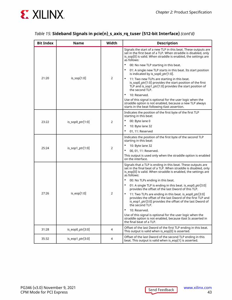
Table 15: Sideband Signals in pcie(n)_s_axis_rq_tuser (512-bit Interface) (cont'd)
Bit Index Name Width Description
21:20 is_sop[1:0] 2
Signals the start of a new TLP in this beat. These outputs areset in the first beat of a TLP. When straddle is disabled, onlyis_sop[0] is valid. When straddle is enabled, the settings areas follows:• 00: No new TLP starting in this beat.• 01: A single new TLP starts in this beat. Its start position
is indicated by is_sop0_ptr[1:0].• 11: Two new TLPs are starting in this beat.
is_sop0_ptr[1:0] provides the start position of the firstTLP and is_sop1_ptr[1:0] provides the start position ofthe second TLP.
• 10: Reserved.Use of this signal is optional for the user logic when thestraddle option is not enabled, because a new TLP alwaysstarts in the beat following tlast assertion.
23:22 is_sop0_ptr[1:0] 2
Indicates the position of the first byte of the first TLPstarting in this beat:• 00: Byte lane 0• 10: Byte lane 32• 01, 11: Reserved
25:24 is_sop1_ptr[1:0] 2
Indicates the position of the first byte of the second TLPstarting in this beat:• 10: Byte lane 32• 00, 01, 11: Reserved.This output is used only when the straddle option is enabledon the interface.
27:26 is_eop[1:0] 2
Signals that a TLP is ending in this beat. These outputs areset in the final beat of a TLP. When straddle is disabled, onlyis_eop[0] is valid. When straddle is enabled, the settings areas follows:• 00: No TLPs ending in this beat.• 01: A single TLP is ending in this beat. is_eop0_ptr[3:0]
provides the offset of the last Dword of this TLP.• 11: Two TLPs are ending in this beat. is_eop0_ptr[3:0]
provides the offset of the last Dword of the first TLP andis_eop1_ptr[3:0] provides the offset of the last Dword ofthe second TLP.
• 10: Reserved.Use of this signal is optional for the user logic when thestraddle option is not enabled, because tlast Is asserted inthe final beat of a TLP.
31:28 is_eop0_ptr[3:0] 4 Offset of the last Dword of the first TLP ending in this beat.This output is valid when is_eop[0] is asserted.
35:32 is_eop1_ptr[3:0] 4 Offset of the last Dword of the second TLP ending in thisbeat. This output is valid when is_eop[1] is asserted.
Chapter 2: Product Specification
PG346 (v3.0) November 9, 2021 www.xilinx.comCPM Mode for PCI Express 43Send Feedback

Table 15: Sideband Signals in pcie(n)_s_axis_rq_tuser (512-bit Interface) (cont'd)
Bit Index Name Width Description
36 discontinue 1
This signal can be asserted by the user application during atransfer if it has detected an error in the data beingtransferred and needs to abort the packet. The core nullifiesthe corresponding TLP on the link to avoid data corruption.The user logic can assert this signal in any beat of a TLPexcept the first beat during its transfer. It can either chooseto terminate the packet prematurely in the cycle where theerror was signaled, or continue until all bytes of the payloadare delivered to the core. In the latter case, the core treatsthe error as sticky for the following beats of the packet, evenif the user logic deasserts the discontinue signal before theend of the packet.The discontinue signal can be asserted only whenpcie(n)_s_axis_rq_tvalid is High. The core samples this signalonly when pcie(n)_s_axis_rq_tready is High. Thus, onceasserted, it should not be deasserted untilpcie(n)_s_axis_rq_tready is High.When the straddle option is enabled on the RQ interface,the user should not start a new TLP in the same beat when aTLP is ending with discontinue asserted.When the core is configured as an Endpoint, this error isalso reported by the core to the Root Complex it is attachedto, using Advanced Error Reporting (AER).
66:61 seq_num0[5:0] 6
The user logic can optionally supply a 6-bit sequencenumber in this field to keep track of the progress of therequest in the core’s transmit pipeline. The core outputs thissequence number on its pcie(n)_rq_seq_num0 orpcie(n)_rq_seq_num1 output when the request TLP hasprogressed to a point in the pipeline where a CompletionTLP from the user logic is not able to pass it.The core samples this field in the first beat of a packet,when pcie(n)_s_axis_rq_tvalid and pcie(n)_s_axis_rq_treadyare both High.This input can be hardwired to 0 when the user logic is notmonitoring the pcie(n)_rq_seq_num* outputs of the core.
72:67 seq_num1[5:0] 6
If there is a second TLP starting in the same beat, the userlogic can optionally provide a 6-bit sequence number forthis TLP on this input. This sequence number is used in thesame manner as seq_num0.The core samples this field in the first beat of a packet,when pcie(n)_s_axis_rq_tvalid and pcie(n)_s_axis_rq_treadyare both High.This input can be hardwired to 0 when the user logic is notmonitoring the pcie(n)_rq_seq_num* outputs of the core.
136:73 parity 64
Odd parity for the 512-bit data. When parity checking isenabled in the core, user logic must set bit i of this bus tothe odd parity computed for byte i ofpcie(n)_s_axis_rq_tdata.On detection of a parity error, the core nullifies thecorresponding TLP on the link and reports it as anUncorrectable Internal Error.These bits can be set to 0 if parity checking is disabled in thecore.
137 PASID TLP Valid 0 1 Indicates PASID TLP is valid for packet 0.pcie_posted_req_delivered is repurposed to pass PASID TLPVALID0 information from the user design.
Chapter 2: Product Specification
PG346 (v3.0) November 9, 2021 www.xilinx.comCPM Mode for PCI Express 44Send Feedback

Table 15: Sideband Signals in pcie(n)_s_axis_rq_tuser (512-bit Interface) (cont'd)
Bit Index Name Width Description138 PASID TLP Valid 1 1 Indicates PASID TLP is valid for packet 1.
pcie_cq_pipeline_empty is repurposed to pass PASID TLPVALID1 information from the user design.
158:139 PASID 0 20 Indicates PASID TLP Prefix for packet 0.Repurpose the following signals to pass PASID 0information from the user design.[139]: pcie_cq_np_user_credit_rcvd.[141:140]: pcie_compl_delivered.[149:142]: pcie_compl_delivered_tag0.[157:150]: pcie_compl_delivered_tag1.user_spare_in[0]: tl_rx_posted_credit_released.
178:159 PASID 1 20 Indicates PASID TLP Prefix for packet 1.Repurpose the following list of signals to pass PASID 1information from the user design.user_spare_in[20:1] indexed as below:[165:159]: tl_rx_posted_payload_credit_released_value.[166]: tl_rx_nonposted_credit_released.[168:167]: tl_rx_nonposted_payload_credit_released_value.[169]: tl_rx_compl_credit_released.[171:170]: tl_rx_compl_header_credit_released_value.[178:172]: tl_rx_compl_payload_credit_released_value.
179 Execute Requested 0 1 Indicates Execute Requested 0.
180 Execute Requested 1 1 Indicates Execute Requested 1.
181 Privileged Mode Requested 0 1 Indicates Privileged Mode Requested 0.
182 Privileged Mode Requested 1 1 Indicates Privileged Mode Requested 1.
Requester Completion Interface
Table 16: Requester Completion Interface Port Descriptions (512-bit Interface)
Name I/O Width Descriptionpcie0_m_axis_rc_tdatapcie1_m_axis_rc_tdata O 512 Transmit data from the PCIe requester completion
interface to the user application.
pcie0_m_axis_rc_tuserpcie1_m_axis_rc_tuser O 161
This is a set of signals containing sideband informationfor the TLP being transferred. These signals are validwhen pcie(n)_m_axis_rc_tvalid is High. The individualsignals in this set are described in the following table.
pcie0_m_axis_rc_tlastpcie1_m_axis_rc_tlast O 1
The core asserts this signal in the last beat of a packet toindicate the end of the packet. When a TLP is transferredin a single beat, the core sets this bit in the first beat ofthe transfer. This output is used only when the straddleoption is disabled. When the straddle option is enabled,the core sets this output permanently to 0.
Chapter 2: Product Specification
PG346 (v3.0) November 9, 2021 www.xilinx.comCPM Mode for PCI Express 45Send Feedback

Table 16: Requester Completion Interface Port Descriptions (512-bit Interface) (cont'd)
Name I/O Width Description
pcie0_m_axis_rc_tkeeppcie1_m_axis_rc_tkeep O 16
The assertion of bit i of this bus during a transferindicates to the user logic that Dword i of thepcie(n)_m_axis_rc_tdata bus contains valid data. The coresets this bit to 1 contiguously for all Dwords starting fromthe first Dword of the descriptor to the last Dword of thepayload. Thus, pcie(n)_m_axis_rc_tkeep is set to all 1s in allbeats of a packet, except in the final beat when the totalsize of the packet is not a multiple of the width of the databus (both in Dwords). This is true for both Dword-alignedand address-aligned modes of payload transfer.These outputs are permanently set to all 1s when thestraddle option is enabled. The user logic must use thesignals in pcie(n)_m_axis_rc_tuser in that case todetermine the start and end of Completion TLPstransferred over the interface.
pcie0_m_axis_rc_tvalidpcie1_m_axis_rc_tvalid O 1
The core asserts this output whenever it is driving validdata on the pcie(n)_m_axis_rc_tdata bus. The core keepsthe valid signal asserted during the transfer of a packet.The user application can pace the data transfer using thepcie(n)_m_axis_rc_tready signal.
pcie0_m_axis_rc_treadypcie1_m_axis_rc_tready I 1
Activation of this signal by the user logic indicates to thePCIe core that the user logic is ready to accept data. Datais transferred across the interface when bothpcie(n)_m_axis_rc_tvalid and pcie(n)_m_axis_rc_tready areasserted in the same cycle.If the user logic deasserts the ready signal when the validsignal is High, the core maintains the data on the bus andkeep the valid signal asserted until the user logic hasasserted the ready signal.
Table 17: Sideband Signals in pcie(n)_m_axis_rc_tuser (512-bit Interface)
Bit Index Name Width Description
63:0 byte_en 64
The client logic may optionally use these byte enable bits todetermine the valid bytes in the payload of a packet beingtransferred. The assertion of bit i of this bus during atransfer indicates to the client that byte i of thepcie(n)_m_axis_cq_tdata bus contains a valid payload byte.This bit is not asserted for descriptor bytes.Although the byte enables can be generated by client logicfrom information in the request descriptor (address andlength), the client has the option of using these signalsdirectly instead of generating them from other interfacesignals. The 1 bits in this bus for the payload of a TLP arealways contiguous.
Chapter 2: Product Specification
PG346 (v3.0) November 9, 2021 www.xilinx.comCPM Mode for PCI Express 46Send Feedback

Table 17: Sideband Signals in pcie(n)_m_axis_rc_tuser (512-bit Interface) (cont'd)
Bit Index Name Width Description
67:64 is_sop[3:0] 4
Signals the start of a new TLP in this beat. These outputs areset in the first beat of a TLP. When straddle is disabled, onlyis_sop[0] is valid and is_sop[3:1] are permanently set to 0.When straddle is enabled, the settings are as follows:• 0000: No new TLP starting in this beat.• 0001: A single new TLP starts in this beat. ts start
position is indicated by is_sop0_ptr[1:0].• 0011: Two new TLPs are starting in this beat.
is_sop0_ptr[1:0] provides the start position of the firstTLP and is_sop1_ptr[1:0] provides the start position ofthe second TLP.
• 0111: Three new TLPs are starting in this beat.is_sop0_ptr[1:0] provides the start position of the firstTLP, is_sop1_ptr[1:0] provides the start position of thesecond TLP, and is_sop2_ptr[1:0] provides the startposition of the third TLP.
• 1111: Four new TLPs are starting in this beat.is_sop0_ptr[1:0] provides the start position of the firstTLP, is_sop1_ptr[1:0] provides the start position of thesecond TLP, is_sop2_ptr[1:0] provides the start positionof the third TLP, and is_sop3_ptr[1:0] provides the startposition of the fourth TLP.
• All other settings are reserved.Use of this signal is optional for the client when the straddleoption is not enabled, because a new TLP always starts inthe beat following pcie(n)_m_axis_rc_tlast assertion.
69:68 is_sop0_ptr[1:0] 2
Indicates the position of the first byte of the first TLPstarting in this beat:• 00: Byte lane 0• 01: Byte lane 16• 10: Byte lane 32• 11: Byte lane 48This field is valid only when the straddle option is enabledon the RC interface. Otherwise, it is set to 0 permanently, asa TLP can only start in bye lane 0.
71:70 is_sop1_ptr[1:0] 2
Indicates the position of the first byte of the second TLPstarting in this beat:• 00: Reserved• 01: Byte lane 16• 10: Byte lane 32• 11: Byte lane 48This output is used only when the straddle option is enabledon the RC interface. The output is permanently set to 0when straddle is disabled.
Chapter 2: Product Specification
PG346 (v3.0) November 9, 2021 www.xilinx.comCPM Mode for PCI Express 47Send Feedback

Table 17: Sideband Signals in pcie(n)_m_axis_rc_tuser (512-bit Interface) (cont'd)
Bit Index Name Width Description
73:72 is_sop2_ptr[1:0] 2
Indicates the position of the first byte of the third TLPstarting in this beat:• 00: Reserved• 01: Reserved• 10: Byte lane 32• 11: Byte lane 48This output is used only when the straddle option is enabledon the RC interface. The output is permanently set to 0when straddle is disabled.
75:74 is_sop3_ptr[1:0] 2
Indicates the position of the first byte of the fourth TLPstarting in this beat:• 00, 01, 10: Reserved• 11: Byte lane 48This output is used only when the straddle option is enabledon the RC interface. The output is permanently set to 0when straddle is disabled.
79:76 is_eop[3:0] 4
Signals that one or more TLPs are ending in this beat onlywhen straddle is enabled. These outputs are set in the finalbeat of a TLP. The settings are as follows:• 0000: No TLPs ending in this beat.• 0001: A single TLP is ending in this beat. is_eop0_ptr[3:0]
provides the offset of the last Dword of this TLP.• 0011: Two TLPs are ending in this beat. is_eop0_ptr[3:0]
provides the offset of the last Dword of the first TLP andis_eop1_ptr[3:0] provides the offset of the last Dword ofthe second TLP.
• 0111: Three TLPs are ending in this beat.is_eop0_ptr[3:0] provides the offset of the last Dword ofthe first TLP, is_eop1_ptr[3:0] provides the offset of thelast Dword of the second TLP, and is_eop2_ptr[3:0]provides the offset of the last Dword of the third TLP.
• 1111: Four TLPs are ending in this beat. is_eop0_ptr[3:0]provides the offset of the last Dword of the first TLP,is_eop1_ptr[3:0] provides the offset of the last Dword ofthe second TLP, is_eop2_ptr[3:0] provides the offset ofthe last Dword of the third TLP, and is_eop3_ptr[3:0]provides the offset of the last Dword of the fourth TLP.
• All other settings are reserved.When the straddle option is disabled, pcie(n)_m_axis_rc_tlastindicates the final beat of a TLP.
83:80 is_eop0_ptr[3:0] 4
Offset of the last Dword of the first TLP ending in this beat.This output is valid when is_eop[0] is asserted.This output is used only when the straddle option is enabledon the RC interface. The output is permanently set to 0when straddle is disabled.
87:84 is_eop1_ptr[3:0] 4
Offset of the last Dword of the second TLP ending in thisbeat. This output is valid when is_eop[1] is asserted.This output is used only when the straddle option is enabledon the RC interface. The output is permanently set to 0when straddle is disabled.
Chapter 2: Product Specification
PG346 (v3.0) November 9, 2021 www.xilinx.comCPM Mode for PCI Express 48Send Feedback

Table 17: Sideband Signals in pcie(n)_m_axis_rc_tuser (512-bit Interface) (cont'd)
Bit Index Name Width Description
91:88 is_eop2_ptr[3:0] 4
Offset of the last Dword of the third TLP ending in this beat.This output is valid when is_eop[2] is asserted.This output is used only when the straddle option is enabledon the RC interface. The output is permanently set to 0when straddle is disabled.
95:92 is_eop3_ptr[3:0] 4
Offset of the last Dword of the fourth TLP ending in thisbeat. This output is valid when is_eop[3] is asserted.This output is used only when the straddle option is enabledon the RC interface. The output is permanently set to 0when straddle is disabled.
96 discontinue 1
This signal is asserted by the core in the last beat of a TLP, ifit has detected an uncorrectable error while reading the TLPpayload from its internal FIFO memory. The clientapplication must discard the entire TLP when such an erroris signaled by the core.This signal is never asserted when the TLP has no payload.It is asserted only in the last beat of the payload transfer,that is when is_eop[0] is High.When the straddle option is enabled, the core does not starta new TLP if it has asserted discontinue in a beat.When the core is configured as an Endpoint, the error is alsoreported by the core to the Root Complex it is attached to,using Advanced Error Reporting (AER).
160:97 parity 64 Odd parity for the 512-bit transmit data. Bit i provides theodd parity computed for byte i of pcie(n)_m_axis_cq_tdata.
Clock and Reset InterfaceFundamental to the operation of the core, the Clock and Reset interface provides the system-level clock and reset to the core as well as the user application clock and reset signal. The tablebelow defines the ports in the Clock and Reset interface of the core.
The pcie(n)_user_clk signal is the clock available in the fabric region. For more informationon clock and reset interface, refer to ‘Clocking’ and ‘Resets’ in "Designing with the Core" chapter.
Note: The pcie0* signals map to PCIe Controller 0, and pcie1* signals map to PCIe Controller 1 in theport descriptions below.
Table 18: Clock and Reset Interface Port Descriptions
Port I/O Width Description
pcie0_user_clkpcie1_user_clk O 1
User clock output (62.5, 125, or 250 MHz)This clock has a fixed frequency and is configured in theVivado® Integrated Design Environment (IDE).
pcie0_user_resetpcie1_user_reset O 1
This signal is deasserted synchronously with respect topcie(n)_user_clk. It is asserted asynchronously with perstassertion.
Chapter 2: Product Specification
PG346 (v3.0) November 9, 2021 www.xilinx.comCPM Mode for PCI Express 49Send Feedback
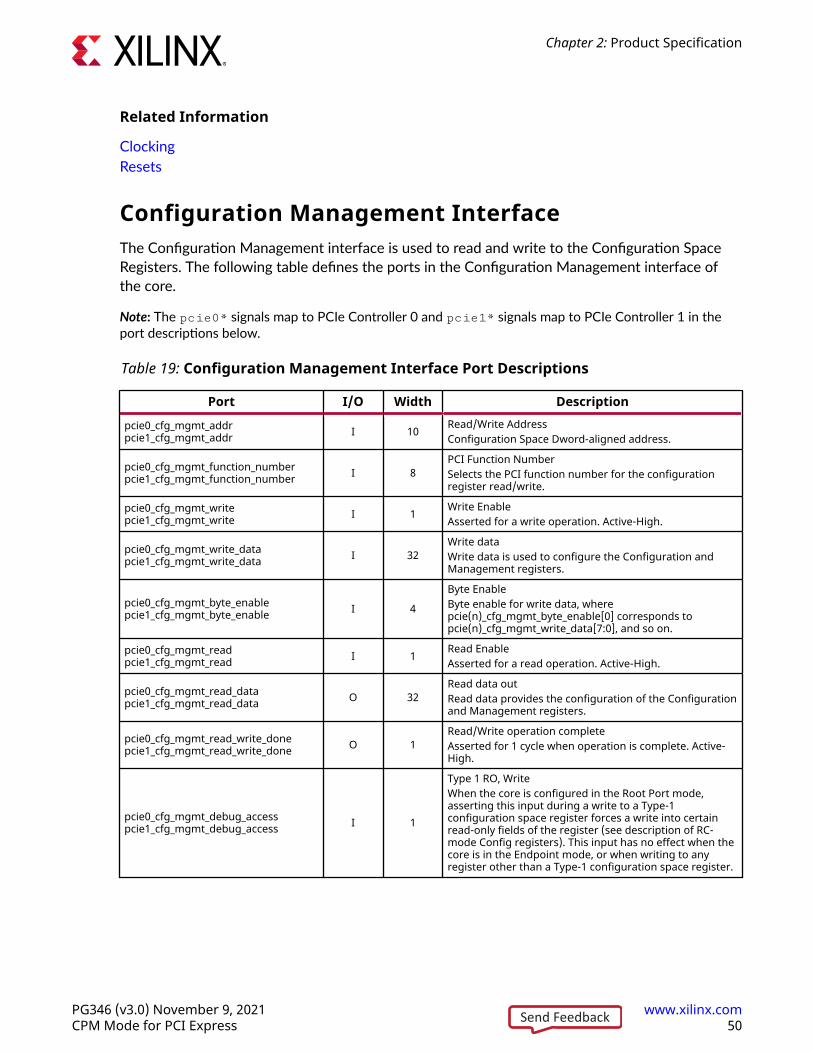
Related Information
ClockingResets
Configuration Management InterfaceThe Configuration Management interface is used to read and write to the Configuration SpaceRegisters. The following table defines the ports in the Configuration Management interface ofthe core.
Note: The pcie0* signals map to PCIe Controller 0 and pcie1* signals map to PCIe Controller 1 in theport descriptions below.
Table 19: Configuration Management Interface Port Descriptions
Port I/O Width Description
pcie0_cfg_mgmt_addrpcie1_cfg_mgmt_addr I 10 Read/Write Address
Configuration Space Dword-aligned address.
pcie0_cfg_mgmt_function_numberpcie1_cfg_mgmt_function_number I 8
PCI Function NumberSelects the PCI function number for the configurationregister read/write.
pcie0_cfg_mgmt_writepcie1_cfg_mgmt_write I 1 Write Enable
Asserted for a write operation. Active-High.
pcie0_cfg_mgmt_write_datapcie1_cfg_mgmt_write_data I 32
Write dataWrite data is used to configure the Configuration andManagement registers.
pcie0_cfg_mgmt_byte_enablepcie1_cfg_mgmt_byte_enable I 4
Byte EnableByte enable for write data, wherepcie(n)_cfg_mgmt_byte_enable[0] corresponds topcie(n)_cfg_mgmt_write_data[7:0], and so on.
pcie0_cfg_mgmt_readpcie1_cfg_mgmt_read I 1 Read Enable
Asserted for a read operation. Active-High.
pcie0_cfg_mgmt_read_datapcie1_cfg_mgmt_read_data O 32
Read data outRead data provides the configuration of the Configurationand Management registers.
pcie0_cfg_mgmt_read_write_donepcie1_cfg_mgmt_read_write_done O 1
Read/Write operation completeAsserted for 1 cycle when operation is complete. Active-High.
pcie0_cfg_mgmt_debug_accesspcie1_cfg_mgmt_debug_access I 1
Type 1 RO, WriteWhen the core is configured in the Root Port mode,asserting this input during a write to a Type-1configuration space register forces a write into certainread-only fields of the register (see description of RC-mode Config registers). This input has no effect when thecore is in the Endpoint mode, or when writing to anyregister other than a Type-1 configuration space register.
Chapter 2: Product Specification
PG346 (v3.0) November 9, 2021 www.xilinx.comCPM Mode for PCI Express 50Send Feedback
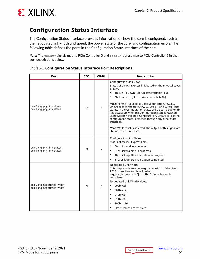
Configuration Status InterfaceThe Configuration Status interface provides information on how the core is configured, such asthe negotiated link width and speed, the power state of the core, and configuration errors. Thefollowing table defines the ports in the Configuration Status interface of the core.
Note: The pcie0* signals map to PCIe Controller 0 and pcie1* signals map to PCIe Controller 1 in theport descriptions below.
Table 20: Configuration Status Interface Port Descriptions
Port I/O Width Description
pcie0_cfg_phy_link_downpcie1_cfg_phy_link_down O 1
Configuration Link DownStatus of the PCI Express link based on the Physical LayerLTSSM.• 1b: Link is Down (LinkUp state variable is 0b)• 0b: Link is Up (LinkUp state variable is 1b)
Note: Per the PCI Express Base Specification, rev. 3.0,LinkUp is 1b in the Recovery, L0, L0s, L1, and L2 cfg_ltssmstates. In the Configuration state, LinkUp can be 0b or 1b.It is always 0b when the Configuration state is reachedusing Detect > Polling > Configuration. LinkUp is 1b if theconfiguration state is reached through any other statetransition.
Note: While reset is asserted, the output of this signal are0b until reset is released.
pcie0_cfg_phy_link_statuspcie1_cfg_phy_link_status O 2
Configuration Link StatusStatus of the PCI Express link.• 00b: No receivers detected• 01b: Link training in progress• 10b: Link up, DL initialization in progress• 11b: Link up, DL initialization completed
pcie0_cfg_negotiated_widthpcie1_cfg_negotiated_width O 3
Negotiated Link WidthThis output indicates the negotiated width of the givenPCI Express Link and is valid whencfg_phy_link_status[1:0] == 11b (DL Initialization iscomplete).Negotiated Link Width values:• 000b = x1• 001b = x2• 010b = x4• 011b = x8• 100b = x16• Other values are reserved.
Chapter 2: Product Specification
PG346 (v3.0) November 9, 2021 www.xilinx.comCPM Mode for PCI Express 51Send Feedback
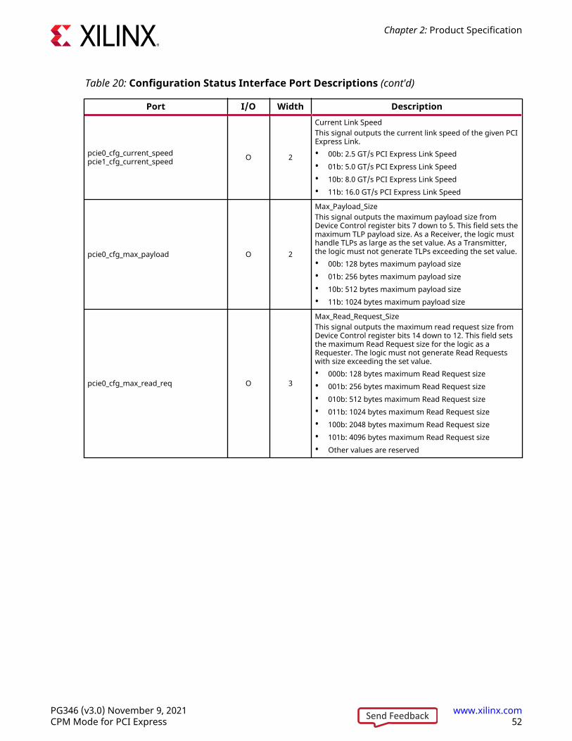
Table 20: Configuration Status Interface Port Descriptions (cont'd)
Port I/O Width Description
pcie0_cfg_current_speedpcie1_cfg_current_speed O 2
Current Link SpeedThis signal outputs the current link speed of the given PCIExpress Link.• 00b: 2.5 GT/s PCI Express Link Speed• 01b: 5.0 GT/s PCI Express Link Speed• 10b: 8.0 GT/s PCI Express Link Speed• 11b: 16.0 GT/s PCI Express Link Speed
pcie0_cfg_max_payload O 2
Max_Payload_SizeThis signal outputs the maximum payload size fromDevice Control register bits 7 down to 5. This field sets themaximum TLP payload size. As a Receiver, the logic musthandle TLPs as large as the set value. As a Transmitter,the logic must not generate TLPs exceeding the set value.• 00b: 128 bytes maximum payload size• 01b: 256 bytes maximum payload size• 10b: 512 bytes maximum payload size• 11b: 1024 bytes maximum payload size
pcie0_cfg_max_read_req O 3
Max_Read_Request_SizeThis signal outputs the maximum read request size fromDevice Control register bits 14 down to 12. This field setsthe maximum Read Request size for the logic as aRequester. The logic must not generate Read Requestswith size exceeding the set value.• 000b: 128 bytes maximum Read Request size• 001b: 256 bytes maximum Read Request size• 010b: 512 bytes maximum Read Request size• 011b: 1024 bytes maximum Read Request size• 100b: 2048 bytes maximum Read Request size• 101b: 4096 bytes maximum Read Request size• Other values are reserved
Chapter 2: Product Specification
PG346 (v3.0) November 9, 2021 www.xilinx.comCPM Mode for PCI Express 52Send Feedback

Table 20: Configuration Status Interface Port Descriptions (cont'd)
Port I/O Width Description
pcie0_cfg_function_status O 16
Configuration Function StatusThese outputs indicate the states of the Commandregister bits in the PCI configuration space of eachfunction. These outputs are used to enable requests andcompletions from the host logic. The assignment of bits isas follows:• Bit 0: Function 0 I/O Space Enable• Bit 1: Function 0 Memory Space Enable• Bit 2: Function 0 Bus Master Enable• Bit 3: Function 0 INTx Disable• Bit 4: Function 1 I/O Space Enable• Bit 5: Function 1 Memory Space Enable• Bit 6: Function 1 Bus Master Enable• Bit 7: Function 1 INTx Disable• Bit 8: Function 2 I/O Space Enable• Bit 9: Function 2 Memory Space Enable• Bit 10: Function 2 Bus Master Enable• Bit 11: Function 2 INTx Disable• Bit 12: Function 3 I/O Space Enable• Bit 13: Function 3 Memory Space Enable• Bit 14: Function 3 Bus Master Enable• Bit 15: Function 3 INTx Disable
pcie0_cfg_vf_statuspcie1_cfg_vf_status O 504
Configuration Virtual Function Status• Bit 0: Virtual function 0: Configured/Enabled by the
software.• Bit 1: Virtual function 0: PCI Command register, Bus
Master Enable.• Bit 2: Virtual function 1: Configured/Enabled by
software.• Bit 3: Virtual function 1: PCI Command register, Bus
Master Enable.
pcie0_cfg_function_power_state O 12
Configuration Function Power StateThese outputs indicate the current power state of thephysical functions. Bits [2:0] capture the power state offunction 0, and bits [5:3] capture that of function 1, and soon. The possible power states are:• 000: D0_uninitialized• 001: D0_active• 010: D1• 100: D3_hot• Other values are reserved.
Chapter 2: Product Specification
PG346 (v3.0) November 9, 2021 www.xilinx.comCPM Mode for PCI Express 53Send Feedback

Table 20: Configuration Status Interface Port Descriptions (cont'd)
Port I/O Width Description
pcie0_cfg_vf_power_statepcie1_cfg_vf_power_state O 756
Configuration Virtual Function Power StateThese outputs indicate the current power state of thevirtual functions. Bits [2:0] capture the power state ofvirtual function 0, and bits [5:3] capture that of virtualfunction 1, and so on. The possible power states are:• 000: D0_uninitialized• 001: D0_active• 010: D1• 100: D3_hot• Other values are reserved.
pcie0_cfg_link_power_statepcie1_cfg_link_power_state O 2
Current power state of the PCI Express link, and is validwhen cfg_phy_link_status[1:0] == 11b (DL Initialization iscomplete).• 00: L0• 01: TX L0s• 10: L1• 11: L2/3 Ready
Chapter 2: Product Specification
PG346 (v3.0) November 9, 2021 www.xilinx.comCPM Mode for PCI Express 54Send Feedback

Table 20: Configuration Status Interface Port Descriptions (cont'd)
Port I/O Width Description
pcie0_cfg_local_error_outpcie1_cfg_local_error_out O 5
Local Error Conditions: Error priority is noted and Priority0 has the highest priority.• 00000b - Reserved• 00001b - Physical Layer Error Detected (Priority 16)• 00010b - Link Replay Timeout (Priority 12)• 00011b - Link Replay Rollover (Priority 13)• 00100b - Link Bad TLP Received (Priority 10)• 00101b - Link Bad DLLP Received (Priority 11)• 00110b - Link Protocol Error (Priority 9)• 00111b - Replay Buffer RAM Correctable ECC Error
(Priority 22)• 01000b - Replay Buffer RAM Uncorrectable ECC Error
(Priority 3)• 01001b - Receive Posted Request RAM Correctable
ECC Error (Priority 20)• 01010b - Receive Posted Request RAM Uncorrectable
ECC Error (Priority 1)• 01011b - Receive Completion RAM Correctable ECC
Error (Priority 21)• 01100b - Receive Completion RAM Uncorrectable ECC
Error (Priority 2)• 01101b - Receive Posted Buffer Overflow Error
(Priority 5)• 01110b - Receive Non Posted Buffer Overflow Error
(Priority 6)• 01111b - Receive Completion Buffer Overflow Error
(Priority 7)• 10000b - Flow Control Protocol Error (Priority 8)• 10001b - Transmit Parity Error Detected (Priority 4)• 10010b - Unexpected Completion Received (Priority
15)• 10011b - Completion Timeout Detected (Priority 14)• 10100b - AXI4ST RQ INTFC Packet Drop (Priority 17)• 10101b - AXI4ST CC INTFC Packet Drop (Priority 18)• 10110b - AXI4ST CQ Poisoned Drop (Priority 19)• 10111b - User Signaled Internal Correctable Error
(Priority 23)• 11000b - User Signaled Internal Uncorrectable Error
(Priority 0)• 11001b - 11111b - Reserved
Chapter 2: Product Specification
PG346 (v3.0) November 9, 2021 www.xilinx.comCPM Mode for PCI Express 55Send Feedback

Table 20: Configuration Status Interface Port Descriptions (cont'd)
Port I/O Width Description
pcie0_cfg_local_error_validpcie1_cfg_local_error_valid O 1
Local Error Conditions Valid: Block activates this outputfor one cycle when any of the errors incfg_local_error_out[4:0] are encountered. When driven 1bcfg_local_error_out[4:0] indicates local error type. Priorityof error reporting (for the case of concurrent errors) isnoted.
Note: This signal may not work for all PCIe Link Width/Speed configurations. Do not rely solely on this signal toindicate an error. Alternatively, you can decode AERregister to accurately detect errors.
pcie0_cfg_rx_pm_statepcie1_cfg_rx_pm_state O 2
Current RX Active State Power Management L0s State:Encoding is listed below and valid when cfg_ltssm_state isindicating L0:• RX_NOT_IN_L0s = 0• RX_L0s_ENTRY = 1• RX_L0s_IDLE = 2• RX_L0s_FTS = 3
pcie0_cfg_tx_pm_statepcie1_cfg_tx_pm_state O 2
Current TX Active State Power Management L0s State:Encoding is listed below and valid when cfg_ltssm_state isindicating L0:• TX_NOT_IN_L0s = 0• TX_L0s_ENTRY = 1• TX_L0s_IDLE = 2• TX_L0s_FTS = 3
Chapter 2: Product Specification
PG346 (v3.0) November 9, 2021 www.xilinx.comCPM Mode for PCI Express 56Send Feedback
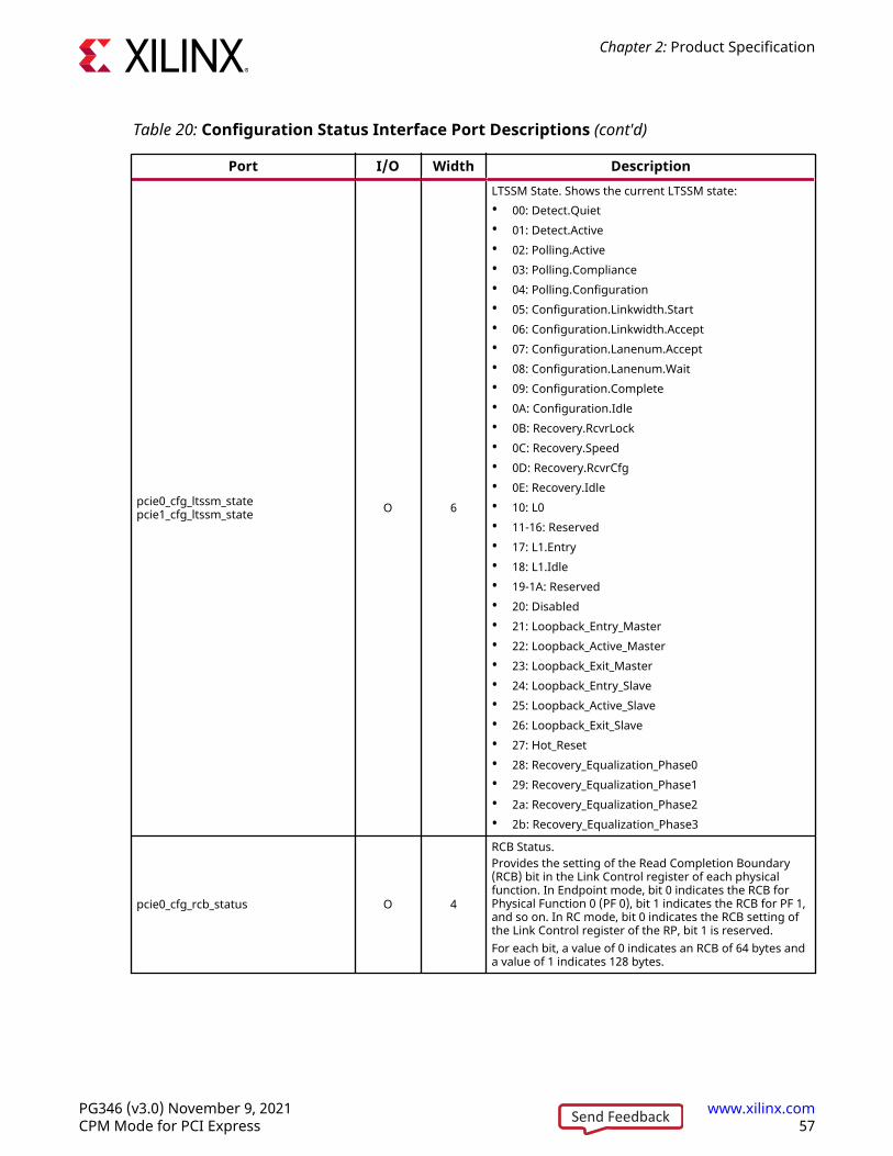
Table 20: Configuration Status Interface Port Descriptions (cont'd)
Port I/O Width Description
pcie0_cfg_ltssm_statepcie1_cfg_ltssm_state O 6
LTSSM State. Shows the current LTSSM state:• 00: Detect.Quiet• 01: Detect.Active• 02: Polling.Active• 03: Polling.Compliance• 04: Polling.Configuration• 05: Configuration.Linkwidth.Start• 06: Configuration.Linkwidth.Accept• 07: Configuration.Lanenum.Accept• 08: Configuration.Lanenum.Wait• 09: Configuration.Complete• 0A: Configuration.Idle• 0B: Recovery.RcvrLock• 0C: Recovery.Speed• 0D: Recovery.RcvrCfg• 0E: Recovery.Idle• 10: L0• 11-16: Reserved• 17: L1.Entry• 18: L1.Idle• 19-1A: Reserved• 20: Disabled• 21: Loopback_Entry_Master• 22: Loopback_Active_Master• 23: Loopback_Exit_Master• 24: Loopback_Entry_Slave• 25: Loopback_Active_Slave• 26: Loopback_Exit_Slave• 27: Hot_Reset• 28: Recovery_Equalization_Phase0• 29: Recovery_Equalization_Phase1• 2a: Recovery_Equalization_Phase2• 2b: Recovery_Equalization_Phase3
pcie0_cfg_rcb_status O 4
RCB Status.Provides the setting of the Read Completion Boundary(RCB) bit in the Link Control register of each physicalfunction. In Endpoint mode, bit 0 indicates the RCB forPhysical Function 0 (PF 0), bit 1 indicates the RCB for PF 1,and so on. In RC mode, bit 0 indicates the RCB setting ofthe Link Control register of the RP, bit 1 is reserved.For each bit, a value of 0 indicates an RCB of 64 bytes anda value of 1 indicates 128 bytes.
Chapter 2: Product Specification
PG346 (v3.0) November 9, 2021 www.xilinx.comCPM Mode for PCI Express 57Send Feedback

Table 20: Configuration Status Interface Port Descriptions (cont'd)
Port I/O Width Description
pcie0_cfg_pl_status_changepcie1_cfg_pl_status_change O 1
This output is used by the core in Root Port mode tosignal one of the following link training-related events:• The link bandwidth changed as a result of the change
in the link width or operating speed and the changewas initiated locally (not by the link partner), withoutthe link going down. This interrupt is enabled by theLink Bandwidth Management Interrupt Enable bit inthe Link Control register. The status of this interruptcan be read from the Link Bandwidth ManagementStatus bit of the Link Status register; or
• The link bandwidth changed autonomously as a resultof the change in the link width or operating speedand the change was initiated by the remote node.This interrupt is enabled by the Link AutonomousBandwidth Interrupt Enable bit in the Link Controlregister. The status of this interrupt can be read fromthe Link Autonomous Bandwidth Status bit of the LinkStatus register; or
• The Link Equalization Request bit in the Link Status 2register was set by the hardware because it received alink equalization request from the remote node. Thisinterrupt is enabled by the Link Equalization InterruptEnable bit in the Link Control 3 register. The status ofthis interrupt can be read from the Link EqualizationRequest bit of the Link Status 2 register.
The pl_interrupt output is not active when the core isconfigured as an Endpoint.
pcie0_cfg_ext_tag_enable O 1 Extended Tag Enable:Per function state of Device ControlRegister Ext Tag (8-Bit) Enable bit.
pcie0_cfg_atomic_requester_enable O 4 Atomic Operation Requester Enable: Per function state ofDevice Control2 Register AtomicOp Requester Enable bit.
pcie0_cfg_10b_tag_requester_enable O 4 10b Tag Requester Enable: Per function state of DeviceControl2 Register 10-Bit Tag Requester Enable bit.
pcie0_pcie_tfc_nph_avpcie1_pcie_tfc_nph_av O 4
This output provides an indication of the currentlyavailable header credit for Non-Posted TLPs on thetransmit side of the core. The user logic can check thisoutput before transmitting a Non-Posted request on therequester request interface, to avoid blocking theinterface when no credit is available. The encodings are:• 0000: No credit available• 0001: 1 credit available• 0010: 2 credits available• ...• 1110: 14 credits available• 1111: 15 or more credits availableBecause of pipeline delays, the value on this output cannot include the credit consumed by the Non-Postedrequests in the last eight cycles or less. The user logicmust adjust the value on this output by the creditconsumed by the Non-Posted requests it sent in theprevious clock cycles, if any.
Chapter 2: Product Specification
PG346 (v3.0) November 9, 2021 www.xilinx.comCPM Mode for PCI Express 58Send Feedback

Table 20: Configuration Status Interface Port Descriptions (cont'd)
Port I/O Width Description
pcie0_pcie_tfc_npd_avpcie1_pcie_tfc_npd_av O 4
This output provides an indication of the currentlyavailable payload credit for Non-Posted TLPs on thetransmit side of the core. The user logic checks thisoutput before transmitting a Non-Posted request on therequester request interface, to avoid blocking theinterface when no credit is available. The encodings are:• 0000: No credit available• 0001: 1 credit available• 0010: 2 credits available• ...• 1110: 14 or more credits available• 1111: 15 or more credits availableBecause of pipeline delays, the value on this output doesnot include the credit consumed by the Non-Postedrequests sent by the user logic in the last eight clockcycles or less. The user logic must adjust the value on thisoutput by the credit consumed by the Non-Postedrequests it sent in the previous clock cycles, if any.
pcie0_rq_tag_avpcie1_rq_tag_av O 4
This output provides an indication of the number of freetags available for allocation to Non-Posted requests onthe PCIe master side of the core. The user logic checksthis output before transmitting a Non-Posted request onthe requester request interface, to avoid blocking theinterface when no tags are available. The encodings are:• 0000: No tags available• 0001: 1 tag available• 0010: 2 tags available• ...• 1110: 14 tags available• 1111: 15 or more tags availableBecause of pipeline delays, the value on this output doesnot include the tags consumed by the Non-Postedrequests sent by the user logic in the last 8 clock cycles orless. The user logic must adjust the value on this outputby the number of Non-Posted requests it sent in theprevious clock cycles, if any.
Configuration Received Message InterfaceThe Configuration Received Message interface indicates to the logic that a decodable messagefrom the link, the parameters associated with the data, and the type of message have beenreceived. The following table defines the ports in the Configuration Received Message interfaceof the core.
Note: Configuration Received Message interface is available only for PCIe Controller 0.
Chapter 2: Product Specification
PG346 (v3.0) November 9, 2021 www.xilinx.comCPM Mode for PCI Express 59Send Feedback
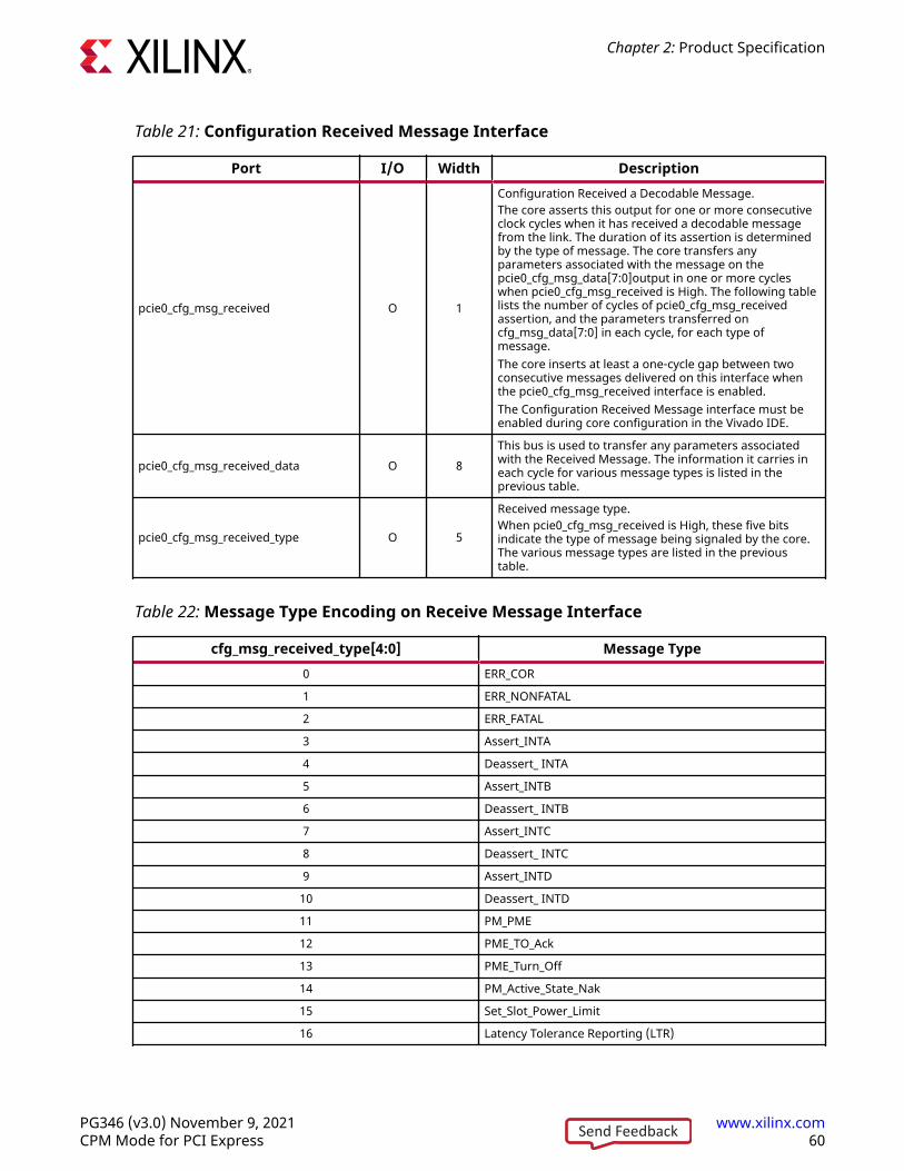
Table 21: Configuration Received Message Interface
Port I/O Width Description
pcie0_cfg_msg_received O 1
Configuration Received a Decodable Message.The core asserts this output for one or more consecutiveclock cycles when it has received a decodable messagefrom the link. The duration of its assertion is determinedby the type of message. The core transfers anyparameters associated with the message on thepcie0_cfg_msg_data[7:0]output in one or more cycleswhen pcie0_cfg_msg_received is High. The following tablelists the number of cycles of pcie0_cfg_msg_receivedassertion, and the parameters transferred oncfg_msg_data[7:0] in each cycle, for each type ofmessage.The core inserts at least a one-cycle gap between twoconsecutive messages delivered on this interface whenthe pcie0_cfg_msg_received interface is enabled.The Configuration Received Message interface must beenabled during core configuration in the Vivado IDE.
pcie0_cfg_msg_received_data O 8This bus is used to transfer any parameters associatedwith the Received Message. The information it carries ineach cycle for various message types is listed in theprevious table.
pcie0_cfg_msg_received_type O 5
Received message type.When pcie0_cfg_msg_received is High, these five bitsindicate the type of message being signaled by the core.The various message types are listed in the previoustable.
Table 22: Message Type Encoding on Receive Message Interface
cfg_msg_received_type[4:0] Message Type0 ERR_COR
1 ERR_NONFATAL
2 ERR_FATAL
3 Assert_INTA
4 Deassert_ INTA
5 Assert_INTB
6 Deassert_ INTB
7 Assert_INTC
8 Deassert_ INTC
9 Assert_INTD
10 Deassert_ INTD
11 PM_PME
12 PME_TO_Ack
13 PME_Turn_Off
14 PM_Active_State_Nak
15 Set_Slot_Power_Limit
16 Latency Tolerance Reporting (LTR)
Chapter 2: Product Specification
PG346 (v3.0) November 9, 2021 www.xilinx.comCPM Mode for PCI Express 60Send Feedback

Table 22: Message Type Encoding on Receive Message Interface (cont'd)
cfg_msg_received_type[4:0] Message Type17 Reserved
18 Unlock
19 Vendor_Defined Type 0
20 Vendor_Defined Type 1
25 – 31 Reserved
Table 23: Message Parameters on Receive Message Interface
Message TypeNumber of cycles of
pcie0_cfg_msg_receivedassertion
Parameter transferred onpcie0_cfg_msg_received_data[7:
0]
ERR_COR, ERR_NONFATAL, ERR_FATAL 2Cycle 1: Requester ID, Bus NumberCycle 2: Requester ID, Device/FunctionNumber
Assert_INTx, Deassert_INTx 2Cycle 1: Requester ID, Bus NumberCycle 2: Requester ID, Device/FunctionNumber
PM_PME, PME_TO_Ack, PME_Turn_off,PM_Active_State_Nak 2
Cycle 1: Requester ID, Bus NumberCycle 2: Requester ID, Device/FunctionNumber
Set_Slot_Power_Limit 6
Cycle 1: Requester ID, Bus NumberCycle 2: Requester ID, Device/FunctionNumberCycle 3: bits [7:0] of payloadCycle 4: bits [15:8] of payloadCycle 5: bits [23:16] of payloadCycle 6: bits [31:24] of payload
Latency Tolerance Reporting (LTR) 6
Cycle 1: Requester ID, Bus NumberCycle 2: Requester ID, Device/FunctionNumberCycle 3: bits [7:0] of Snoop LatencyCycle 4: bits [15:8] of Snoop LatencyCycle 5: bits [7:0] of No-Snoop LatencyCycle 6: bits [15:8] of No-Snoop Latency
Unlock 2Cycle 1: Requester ID, Bus NumberCycle 2: Requester ID, Device/FunctionNumber
Vendor_Defined Type 0 4 cycles when no data present, 8 cycleswhen data present.
Cycle 1: Requester ID, Bus NumberCycle 2: Requester ID, Device/FunctionNumberCycle 3: Vendor ID[7:0]Cycle 4: Vendor ID[15:8]Cycle 5: bits [7:0] of payloadCycle 6: bits [15:8] of payloadCycle 7: bits [23:16] of payloadCycle 8: bits [31:24] of payload
Chapter 2: Product Specification
PG346 (v3.0) November 9, 2021 www.xilinx.comCPM Mode for PCI Express 61Send Feedback

Table 23: Message Parameters on Receive Message Interface (cont'd)
Message TypeNumber of cycles of
pcie0_cfg_msg_receivedassertion
Parameter transferred onpcie0_cfg_msg_received_data[7:
0]
Vendor_Defined Type 1 4 cycles when no data present, 8 cycleswhen data present.
Cycle 1: Requester ID, Bus NumberCycle 2: Requester ID, Device/FunctionNumberCycle 3: Vendor ID[7:0]Cycle 4: Vendor ID[15:8]Cycle 5: bits [7:0] of payloadCycle 6: bits [15:8] of payloadCycle 7: bits [23:16] of payloadCycle 8: bits [31:24] of payload
Configuration Transmit Message InterfaceThe Configuration Transmit Message interface is used by the user application to transmitmessages to the core. The user application supplies the transmit message type and datainformation to the core, which responds with the done signal. The following table defines theports in the Configuration Transmit Message interface of the core.
Note: The pcie0* signals map to PCIe Controller 0 and pcie1* signals map to PCIe Controller 1 in theport descriptions below.
Table 24: Configuration Transmit Message Interface
Port I/O Width Description
pcie0_cfg_msg_transmitpcie1_cfg_msg_transmit I 1
Configuration Transmit Encoded Message.This signal is asserted together withcfg_msg_transmit_type, which supplies the encodedmessage type and cfg_msg_transmit_data, which suppliesoptional data associated with the message, untilcfg_msg_transmit_done is asserted in response.
pcie0_cfg_msg_transmit_typepcie1_cfg_msg_transmit_type I 3
Configuration Transmit Encoded Message Type.Indicates the type of PCI Express message to betransmitted. Encodings supported are:• 000b: Latency Tolerance Reporting (LTR)• 001b: Optimized Buffer Flush/Fill (OBFF)• 010b: Set Slot Power Limit (SSPL)• 011b: Power Management (PM PME)• 100b -111b: Reserved
Chapter 2: Product Specification
PG346 (v3.0) November 9, 2021 www.xilinx.comCPM Mode for PCI Express 62Send Feedback

Table 24: Configuration Transmit Message Interface (cont'd)
Port I/O Width Description
pcie0_cfg_msg_transmit_datapcie1_cfg_msg_transmit_data I 32
Configuration Transmit Encoded Message Data.Indicates message data associated with particularmessage type.000b: LTR• cfg_msg_transmit_data[31] < Snoop Latency Req• cfg_msg_transmit_data[30:29] <= Repurposing to pass
PASID information. assigned tos_axis_rq_tuser[182:181] inside the IP.
• cfg_msg_transmit_data[28:26] < Snoop Latency Scale• cfg_msg_transmit_data[25:16] < Snoop Latency Value• cfg_msg_transmit_data[15] < No-Snoop Latency
Requirement• cfg_msg_transmit_data[14:13] <= Repurposing to pass
PASID information. assigned tos_axis_rq_tuser[180:179] inside the IP.
• cfg_msg_transmit_data[12:10] < No-Snoop LatencyScale
• cfg_msg_transmit_data[9:0] < No-Snoop Latency Value001b: Reserved.010b: SSPL• cfg_msg_transmit_data[9:0] < {Slot Power Limit Scale,
Slot Power Limit Value}011b: PM_PME
• cfg_msg_transmit_data[7:0] <= 8'h00-8'hFFPF0-3 - 8'h00-8'h03 Other encodings are reserved
100b - 111b: Reserved
pcie0_cfg_msg_transmit_done O 1Configuration Transmit Encoded Message Done.Asserted in response to cfg_mg_transmit assertion, for 1cycle after the request is complete.
Configuration Flow Control InterfaceThe following table defines the ports in the Configuration Flow Control interface of the core.
Note: The pcie0* signals map to PCIe Controller 0 and pcie1* signals map to PCIe Controller 1 in theport descriptions below.
Table 25: Configuration Flow Control Interface
Port I/O Width Description
pcie0_cfg_fc_phpcie1_cfg_fc_ph O 8
Posted Header Flow Control Credits.This output provides the number of Posted Header FlowControl Credits. This multiplexed output can be used tobring out various flow control parameters and variablesrelated to Posted Header Credit maintained by the core.The flow control information to bring out on this core isselected by the cfg_fc_sel[2:0] input.
Chapter 2: Product Specification
PG346 (v3.0) November 9, 2021 www.xilinx.comCPM Mode for PCI Express 63Send Feedback

Table 25: Configuration Flow Control Interface (cont'd)
Port I/O Width Description
pcie0_cfg_fc_ph_scalepcie1_cfg_fc_ph_scale O 2
Posted Header Flow Control Credits ScaleThis output provides the scale of Posted Header FlowControl Credit number (cfg_fc_ph). The flow controlinformation to bring out on this core is selected by thecfg_fc_sel[2:0] input.
pcie0_cfg_fc_pdpcie1_cfg_fc_pd O 12
Posted Data Flow Control Credits.This output provides the number of Posted Data FlowControl Credits. This multiplexed output can be used tobring out various flow control parameters and variablesrelated to Posted Data Credit maintained by the core. Theflow control information to bring out on this core isselected by the cfg_fc_sel[2:0] input.
pcie0_cfg_fc_pd_scalepcie1_cfg_fc_pd_scale O 2
Posted Data Flow Control Credits ScaleThis output provides the scale of Posted Data FlowControl Credit number (cfg_fc_pd). The flow controlinformation to bring out on this core is selected by thecfg_fc_sel[2:0] input.
pcie0_cfg_fc_nphpcie1_cfg_fc_nph O 8
Non-Posted Header Flow Control Credits.This output provides the number of Non-Posted HeaderFlow Control Credits. This multiplexed output can be usedto bring out various flow control parameters andvariables related to Non-Posted Header Creditmaintained by the core. The flow control information tobring out on this core is selected by the cfg_fc_sel[2:0]input.
pcie0_cfg_fc_nph_scalepcie1_cfg_fc_nph_scale O 2
Non-Posted Header Flow Control Credits ScaleThis output provides the scale of Non-Posted Header FlowControl Credit number (cfg_fc_nph). The flow controlinformation to bring out on this core is selected by thecfg_fc_sel[2:0] input.
pcie0_cfg_fc_npdpcie1_cfg_fc_npd O 12
Non-Posted Data Flow Control Credits.This output provides the number of Non-Posted DataFlow Control Credits. This multiplexed output can be usedto bring out various flow control parameters andvariables related to Non-Posted Data Credit maintainedby the core. The flow control information to bring out onthis core is selected by the cfg_fc_sel[2:0] input.
pcie0_cfg_fc_npd_scalepcie1_cfg_fc_npd_scale O 2
Non-Posted Data Flow Control Credits ScaleThis output provides the scale of Non-Posted Data FlowControl Credit number (cfg_fc_npd). The flow controlinformation to bring out on this core is selected by thecfg_fc_sel[2:0] input.
pcie0_cfg_fc_cplh O 8
Completion Header Flow Control Credits.This output provides the number of Completion HeaderFlow Control Credits. This multiplexed output can be usedto bring out various flow control parameters andvariables related to Completion Header Credit maintainedby the core. The flow control information to bring out onthis core is selected by the cfg_fc_sel[2:0] input.
pcie0_cfg_fc_cplh_scale O 2
Completion Header Flow Control Credit ScaleThis output provides the scale of Completion Header FlowControl Credit number (cfg_fc_cplh). The flow controlinformation to bring out on this core is selected by thecfg_fc_sel[2:0] input.
Chapter 2: Product Specification
PG346 (v3.0) November 9, 2021 www.xilinx.comCPM Mode for PCI Express 64Send Feedback

Table 25: Configuration Flow Control Interface (cont'd)
Port I/O Width Description
pcie0_cfg_fc_cpld O 12
Completion Data Flow Control Credits.This output provides the number of Completion DataFlow Control Credits. This multiplexed output can be usedto bring out various flow control parameters andvariables related to Completion Data Credit maintainedby the core. The flow control information to bring out onthis core is selected by the cfg_fc_sel[2:0].
pcie0_cfg_fc_cpld_scale O 2
Completion Data Flow Control Credit ScaleThis output provides the scale of Completion Data FlowControl Credit number (cfg_fc_cpld). The flow controlinformation to bring out on this core is selected by thecfg_fc_sel[2:0] input.
pcie0_cfg_fc_vc_selpcie1_cfg_fc_vc_sel I 1
Flow Control Informational Virtual Channel Select: Selectsthe Virtual Channel for the type of flow controlinformation presented on the trn_fc_* signals. Possiblevalues:0b = VC01b = VC1
pcie0_cfg_fc_selpcie1_cfg_fc_sel I 3
Flow Control Informational Select.These inputs select the type of flow control to bring outon the cfg_fc_* outputs of the core. The various flowcontrol parameters and variables that can be accessed forthe different settings of these inputs are:• 000: Receive credit limit to link partner (rlimit)• 001: Transmit credits consumed (tconsumed) & wide
posted and completion• 010: Receive credits consumed by link partner
(rconsumed)• 011: Transmit credits consumed (tconsumed) wide
nonposted and completion• 100: Transmit user credits available (tlimit -
tconsumed)• 101: Transmit credit limit (tlimit)• 110: Transmit credits consumed (tconsumed)• 111: Receive free 32B word countThis value represents the actual unused credits in thereceiver FIFO, and the recommendation is to use it only asan approximate indication of receiver FIFO fullness,relative to the initial credit limit value advertized, such as,¼ full, ½ full, ¾ full, full.Infinite credit for transmit credits available (cfg_fc_sel ==3'b100) is signaled as 8'h80, 12'h800 for header and datacredits, respectively. For all other cfg_fc_sel selections,infinite credit is signaled as 8'h00, 12'h000, respectively,for header and data categories.
Configuration Control InterfaceThe Configuration Control interface signals allow a broad range of information exchangebetween the user application and the core. The user application uses this interface to do thefollowing:
Chapter 2: Product Specification
PG346 (v3.0) November 9, 2021 www.xilinx.comCPM Mode for PCI Express 65Send Feedback
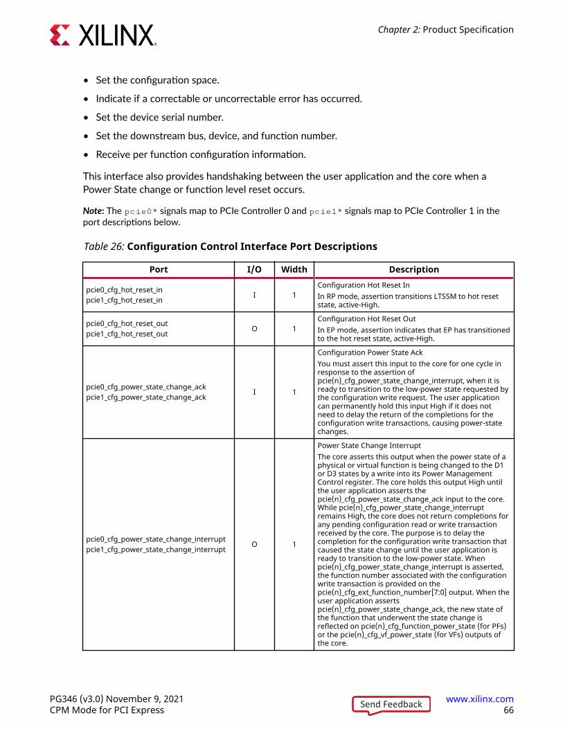
• Set the configuration space.
• Indicate if a correctable or uncorrectable error has occurred.
• Set the device serial number.
• Set the downstream bus, device, and function number.
• Receive per function configuration information.
This interface also provides handshaking between the user application and the core when aPower State change or function level reset occurs.
Note: The pcie0* signals map to PCIe Controller 0 and pcie1* signals map to PCIe Controller 1 in theport descriptions below.
Table 26: Configuration Control Interface Port Descriptions
Port I/O Width Description
pcie0_cfg_hot_reset_inpcie1_cfg_hot_reset_in I 1
Configuration Hot Reset InIn RP mode, assertion transitions LTSSM to hot resetstate, active-High.
pcie0_cfg_hot_reset_outpcie1_cfg_hot_reset_out O 1
Configuration Hot Reset OutIn EP mode, assertion indicates that EP has transitionedto the hot reset state, active-High.
pcie0_cfg_power_state_change_ackpcie1_cfg_power_state_change_ack I 1
Configuration Power State AckYou must assert this input to the core for one cycle inresponse to the assertion ofpcie(n)_cfg_power_state_change_interrupt, when it isready to transition to the low-power state requested bythe configuration write request. The user applicationcan permanently hold this input High if it does notneed to delay the return of the completions for theconfiguration write transactions, causing power-statechanges.
pcie0_cfg_power_state_change_interruptpcie1_cfg_power_state_change_interrupt O 1
Power State Change InterruptThe core asserts this output when the power state of aphysical or virtual function is being changed to the D1or D3 states by a write into its Power ManagementControl register. The core holds this output High untilthe user application asserts thepcie(n)_cfg_power_state_change_ack input to the core.While pcie(n)_cfg_power_state_change_interruptremains High, the core does not return completions forany pending configuration read or write transactionreceived by the core. The purpose is to delay thecompletion for the configuration write transaction thatcaused the state change until the user application isready to transition to the low-power state. Whenpcie(n)_cfg_power_state_change_interrupt is asserted,the function number associated with the configurationwrite transaction is provided on thepcie(n)_cfg_ext_function_number[7:0] output. When theuser application assertspcie(n)_cfg_power_state_change_ack, the new state ofthe function that underwent the state change isreflected on pcie(n)_cfg_function_power_state (for PFs)or the pcie(n)_cfg_vf_power_state (for VFs) outputs ofthe core.
Chapter 2: Product Specification
PG346 (v3.0) November 9, 2021 www.xilinx.comCPM Mode for PCI Express 66Send Feedback

Table 26: Configuration Control Interface Port Descriptions (cont'd)
Port I/O Width Description
pcie0_cfg_err_cor_inpcie1_cfg_err_cor_in I 1
Correctable Error DetectedThe user application activates this input for one cycle toindicate a correctable error detected within the userlogic that needs to be reported as an internal errorthrough the PCI Express Advanced Error Reporting(AER) mechanism. In response, the core sets theCorrected Internal Error Status bit in the AERCorrectable Error Status register of all enabledfunctions, and also sends an error message if enabledto do so. This error is not considered function-specific.
pcie0_cfg_err_cor_outpcie1_cfg_err_cor_out O 1
Correctable Error DetectedIn the Endpoint mode, the Block activates this outputfor one cycle when it has detected a correctable errorand its reporting is not masked. When multiplefunctions are enabled, this is the logical OR of thecorrectable error status bits in the Device StatusRegisters of all functions.
pcie0_cfg_err_fatal_outpcie1_cfg_err_fatal_out O 1
Fatal Error DetectedIn the Endpoint mode, the block activates this outputfor one cycle when it has detected a fatal error and itsreporting is not masked. When multiple functions areenabled, this output is the logical OR of the fatal errorstatus bits in the Device Status Registers of allfunctions.In the Root Port mode, this output is activated ondetection of a local fatal error, when its reporting is notmasked. This output does not respond to any errorssignaled by remote devices using PCI Express errormessages. These error messages are delivered to theuser through the message interface.
pcie0_cfg_err_nonfatal_outpcie1_cfg_err_nonfatal_out O 1
Non Fatal Error DetectedIn the Endpoint mode, the block activates this outputfor one cycle when it has detected a non fatal error andits reporting is not masked. When multiple functionsare enabled, this output is the logical OR of the nonfatal error status bits in the Device Status Registers ofall functions.In the Root Port mode, this output is activated ondetection of a local non fatal error, when its reporting isnot masked. This output does not respond to anyerrors signaled by remote devices using PCI Expresserror messages. These error messages are deliveredthrough the message interface.
pcie0_cfg_err_uncor_inpcie1_cfg_err_uncor_in I 1
Uncorrectable Error DetectedThe user application activates this input for one cycle toindicate a uncorrectable error detected within the userlogic that needs to be reported as an internal errorthrough the PCI Express Advanced Error Reportingmechanism. In response, the core sets the uncorrectedInternal Error Status bit in the AER Uncorrectable ErrorStatus register of all enabled functions, and also sendsan error message if enabled to do so. This error is notconsidered function-specific.
Chapter 2: Product Specification
PG346 (v3.0) November 9, 2021 www.xilinx.comCPM Mode for PCI Express 67Send Feedback
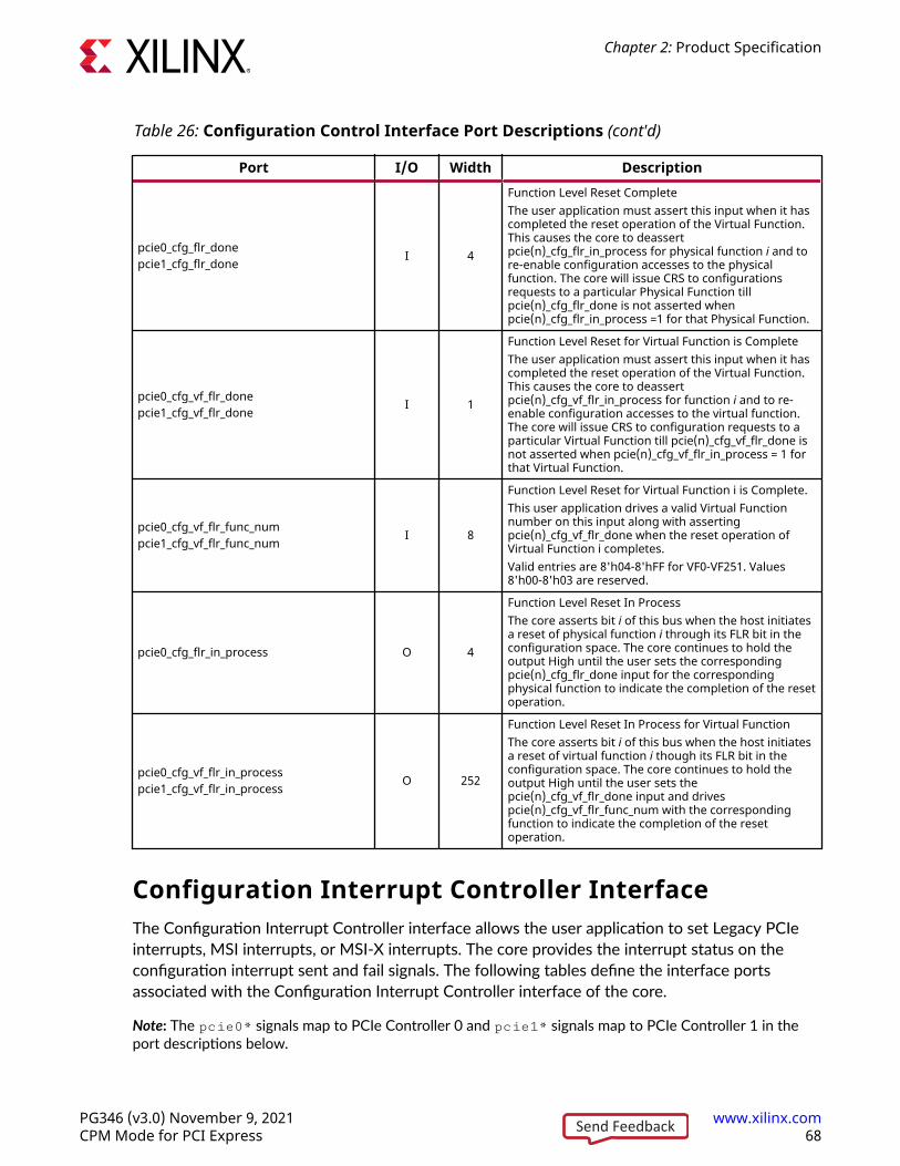
Table 26: Configuration Control Interface Port Descriptions (cont'd)
Port I/O Width Description
pcie0_cfg_flr_donepcie1_cfg_flr_done I 4
Function Level Reset CompleteThe user application must assert this input when it hascompleted the reset operation of the Virtual Function.This causes the core to deassertpcie(n)_cfg_flr_in_process for physical function i and tore-enable configuration accesses to the physicalfunction. The core will issue CRS to configurationsrequests to a particular Physical Function tillpcie(n)_cfg_flr_done is not asserted whenpcie(n)_cfg_flr_in_process =1 for that Physical Function.
pcie0_cfg_vf_flr_donepcie1_cfg_vf_flr_done I 1
Function Level Reset for Virtual Function is CompleteThe user application must assert this input when it hascompleted the reset operation of the Virtual Function.This causes the core to deassertpcie(n)_cfg_vf_flr_in_process for function i and to re-enable configuration accesses to the virtual function.The core will issue CRS to configuration requests to aparticular Virtual Function till pcie(n)_cfg_vf_flr_done isnot asserted when pcie(n)_cfg_vf_flr_in_process = 1 forthat Virtual Function.
pcie0_cfg_vf_flr_func_numpcie1_cfg_vf_flr_func_num I 8
Function Level Reset for Virtual Function i is Complete.This user application drives a valid Virtual Functionnumber on this input along with assertingpcie(n)_cfg_vf_flr_done when the reset operation ofVirtual Function i completes.Valid entries are 8'h04-8'hFF for VF0-VF251. Values8'h00-8'h03 are reserved.
pcie0_cfg_flr_in_process O 4
Function Level Reset In ProcessThe core asserts bit i of this bus when the host initiatesa reset of physical function i through its FLR bit in theconfiguration space. The core continues to hold theoutput High until the user sets the correspondingpcie(n)_cfg_flr_done input for the correspondingphysical function to indicate the completion of the resetoperation.
pcie0_cfg_vf_flr_in_processpcie1_cfg_vf_flr_in_process O 252
Function Level Reset In Process for Virtual FunctionThe core asserts bit i of this bus when the host initiatesa reset of virtual function i though its FLR bit in theconfiguration space. The core continues to hold theoutput High until the user sets thepcie(n)_cfg_vf_flr_done input and drivespcie(n)_cfg_vf_flr_func_num with the correspondingfunction to indicate the completion of the resetoperation.
Configuration Interrupt Controller InterfaceThe Configuration Interrupt Controller interface allows the user application to set Legacy PCIeinterrupts, MSI interrupts, or MSI-X interrupts. The core provides the interrupt status on theconfiguration interrupt sent and fail signals. The following tables define the interface portsassociated with the Configuration Interrupt Controller interface of the core.
Note: The pcie0* signals map to PCIe Controller 0 and pcie1* signals map to PCIe Controller 1 in theport descriptions below.
Chapter 2: Product Specification
PG346 (v3.0) November 9, 2021 www.xilinx.comCPM Mode for PCI Express 68Send Feedback

Legacy Interrupt Interface
Table 27: Legacy Interrupt Interface Port Descriptions
Name I/O Width Description
pcie0_cfg_interrupt_intpcie1_cfg_interrupt_int I 4
Configuration INTx Vector: When the core is configuredas EP, these four inputs are used by the user applicationto signal an interrupt from any of its PCI Functions to theRC using the Legacy PCI Express Interrupt Deliverymechanism of PCI Express. These four inputs correspondto INTA, INTB, INTC, and INTD of the PCI bus, respectively.Asserting one of these signals causes the core to send outan Assert_INTx message, and deasserting the signalcauses the core to transmit a Deassert_INTx message.
pcie0_cfg_interrupt_sentpcie1_cfg_interrupt_sent O 1
Configuration INTx Sent: A pulse on this output indicatesthat the core has sent an INTx Assert or Deassertmessage in response to a change in the state of one ofthe pcie(n)_cfg_interrupt_int inputs.
pcie0_cfg_interrupt_pendingpcie1_cfg_interrupt_pending I 4
Configuration INTx Interrupt Pending: Per Functionindication of a pending interrupt from the user.pcie(n)_cfg_interrupt_pending[0] corresponds to Function#0. Each of these inputs is connected to the InterruptPending bits of the PCI Status Register of thecorresponding Function.
MSI Interrupt Interface
Table 28: MSI Interrupt Interface Port Descriptions
Name I/O Width Description
pcie0_cfg_msi_enable O 4
Configuration Interrupt MSI Function EnabledIndicates that the Message Signaling Interrupt(MSI) messaging is enabled, per Function. Theseoutputs reflect the setting of the MSI Enable bits inthe MSI Control Register of Physical Functions 0 – 3.
pcie0_cfg_msi_mint_vectorpcie1_cfg_msi_mint_vector I 32
Configuration Interrupt MSI VectorWhen configured in the Endpoint mode to supportMSI interrupts, these inputs are used to signal the32 distinct interrupt conditions associated with aPCI Function (Physical or Virtual) from the userlogic to the core. The Function number must bespecified on the inputpcie(n)_cfg_msi_function_number. After placing theFunction number on the inputpcie(n)_cfg_msi_function_number, the user logicmust activateone of these signals for one cycle totransmit an interrupt.The user logic must notactivate more than one of the 32 interrupt inputs inthe same cycle. The core internally registers theinterrupt condition on the 0-to-1 transition of anybit in pcie(n)_cfg_msi_mint_vector. After assertingan interrupt, the user logic must wait for thepcie0_cfg_msi_sent or pcie0_cfg_msi_fail indicationfrom the core before asserting a new interrupt.
Chapter 2: Product Specification
PG346 (v3.0) November 9, 2021 www.xilinx.comCPM Mode for PCI Express 69Send Feedback

Table 28: MSI Interrupt Interface Port Descriptions (cont'd)
Name I/O Width Description
pcie0_cfg_msi_function_numberpcie1_cfg_msi_function_number I 8
Configuration MSI Initiating FunctionIndicates the Endpoint Function # initiating the MSIinterrupt.• 8'h00 – 8'h03: PF 0 – PF 3• 8’h04 – 8’hFF: VF 0 – VF 252• Other encodings are reserved.
pcie0_cfg_msi_sent O 1
Configuration Interrupt MSI Interrupt SentThe core generates a one-cycle pulse on thisoutput to signal that an MSI interrupt message hasbeen transmitted on the link. The user logic mustwait for this pulse before signaling anotherinterrupt condition to the core.
pcie0_cfg_msi_fail O 1
Configuration Interrupt MSI Interrupt OperationFailedA one-cycle pulse on this output indicates that anMSI interrupt message was aborted beforetransmission on the link. The user logic mustretransmit the MSI or MSI-X interrupt in this case.
pcie0_cfg_msi_mmenable O 12
Configuration Interrupt MSI Function MultipleMessage EnableWhen the core is configured in the Endpoint modeto support MSI interrupts, these outputs are drivenby the 'Multiple Message Enable' bits of the MSIControl Register associated with PhysicalFunctions. These bits encode the number ofallocated MSI interrupt vectors for thecorresponding Function. Bits [2:0] correspond toPhysical Function 0, bits [5:3] correspond to PF 1,and so on. The valid encodings of the 3 bits are:• 000b: 1 vector• 001b: 2 vectors• 010b: 4 vectors• 011b: 8 vectors• 100b: 16 vectors• 101b: 32 vectors
pcie0_cfg_msi_pending_statuspcie1_cfg_msi_pending_status I 32
Configuration MSI Interrupt Pending StatusThese inputs are provided for the user to indicatethe interrupt pending status of the MSI interruptsassociated with the Physical Functions. When thestatus of a MSI interrupt associated with a PFchanges, the user must place the new interruptstatus on these inputs, along with thecorresponding Function number on thepcie(n)_cfg_msi_pending_status_function_numinput, and activate thepcie(n)_cfg_msi_pending_status_data_enable inputfor one cycle. The core then latches the new statusin its MSI Pending Bits Register of thecorresponding Physical Function.
Chapter 2: Product Specification
PG346 (v3.0) November 9, 2021 www.xilinx.comCPM Mode for PCI Express 70Send Feedback

Table 28: MSI Interrupt Interface Port Descriptions (cont'd)
Name I/O Width Description
pcie0_cfg_msi_pending_status_function_numpcie1_cfg_msi_pending_status_function_num I 2
Configuration Interrupt MSI Pending TargetFunction Number• 00 = PF 0• 01 = PF 1• 10 = PF 2• 11 = PF 3This input is used to identify the Function numberwhen the user places interrupt status on thepcie(n)_cfg_msi_pending_status inputs.
pcie0_cfg_msi_pending_status_data_enablepcie1_cfg_msi_pending_status_data_enable Input 1
Configuration Interrupt MSI Pending Data ValidThe user application asserts this signal togetherwith pcie(n)_cfg_msi_pending_status andpcie(n)_cfg_msi_pending_status_function_numvalues to update the MSI Pending Bits in thecorresponding function.
pcie0_cfg_msi_mask_update O 1
Configuration Interrupt MSI Function MaskUpdatedThe SR-IOV core asserts this for 1 cycle when theMSI Mask Register of any enabled PFs has changedits value. The user can then read the new masksettings from the pcie(n)_cfg_msi_data outputs.
pcie0_cfg_msi_selectpcie1_cfg_msi_select Input 2
Configuration Interrupt MSI SelectThese inputs are used to select the Functionnumber for reading the MSI Mask Register settingfrom the core. Values 0 – 3 correspond to PhysicalFunctions 0 – 3, respectively. The mask MSI MaskRegister contents of the selected PF appear on theoutput pcie(n)_cfg_msi_data after one cycle.
pcie0_cfg_msi_datapcie1_cfg_msi_data O 32
Configuration Interrupt MSI DataThese output reflect the MSI Mask Register settingof the Physical Function selected by thepcie(n)_cfg_msi_select input.
pcie0_cfg_msi_attrpcie1_cfg_msi_attr I 3
Configuration Interrupt MSI/MSI-X TLP AttributeThese bits enable you to set the Attribute bits thatare used for both MSI and MSI-X interruptrequests.• Bit 0 is the No Snoop bit.• Bit 1 is the Relaxed Ordering bit.• Bit 2 is the ID-Based Ordering bit.The core samples these bits on a 0-to-1 transitionon pcie(n)_cfg_msi_mint_vector bits (when usingMSI) or pcie(n)_cfg_msix_int (when using MSI-X).
MSI-X Interrupt Interface
Table 29: MSI-X Interrupt External Interface Port Descriptions
Name I/O Width Description
pcie0_cfg_msix_enable O 4Configuration Interrupt MSI-X Function EnabledThese outputs reflect the setting of the MSI-X Enable bitsof the MSI-X Control Register of Physical Functions 0 – 3.
Chapter 2: Product Specification
PG346 (v3.0) November 9, 2021 www.xilinx.comCPM Mode for PCI Express 71Send Feedback
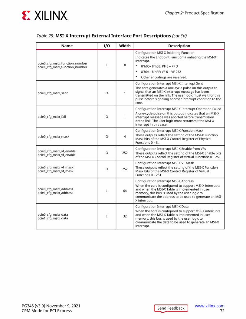
Table 29: MSI-X Interrupt External Interface Port Descriptions (cont'd)
Name I/O Width Description
pcie0_cfg_msix_function_numberpcie1_cfg_msix_function_number I 8
Configuration MSI-X Initiating FunctionIndicates the Endpoint Function # initiating the MSI-Xinterrupt.• 8'h00– 8'h03: PF 0 – PF 3• 8’h04– 8’hFF: VF 0 – VF 252• Other encodings are reserved.
pcie0_cfg_msix_sent O 1
Configuration Interrupt MSI-X Interrupt SentThe core generates a one-cycle pulse on this output tosignal that an MSI-X interrupt message has beentransmitted on the link. The user logic must wait for thispulse before signaling another interrupt condition to thecore.
pcie0_cfg_msix_fail O 1
Configuration Interrupt MSI-X Interrupt Operation FailedA one-cycle pulse on this output indicates that an MSI-Xinterrupt message was aborted before transmissiononthe link. The user logic must retransmit the MSI-Xinterrupt in this case.
pcie0_cfg_msix_mask O 4
Configuration Interrupt MSI-X Function MaskThese outputs reflect the setting of the MSI-X FunctionMask bits of the MSI-X Control Register of PhysicalFunctions 0 – 3.
pcie0_cfg_msix_vf_enablepcie1_cfg_msix_vf_enable O 252
Configuration Interrupt MSI-X Enable from VFsThese outputs reflect the setting of the MSI-X Enable bitsof the MSI-X Control Register of Virtual Functions 0 – 251.
pcie0_cfg_msix_vf_maskpcie1_cfg_msix_vf_mask O 252
Configuration Interrupt MSI-X VF MaskThese outputs reflect the setting of the MSI-X FunctionMask bits of the MSI-X Control Register of VirtualFunctions 0 – 251.
pcie0_cfg_msix_addresspcie1_cfg_msix_address I 64
Configuration Interrupt MSI-X AddressWhen the core is configured to support MSI-X interruptsand when the MSI-X Table is implemented in usermemory, this bus is used by the user logic tocommunicate the address to be used to generate an MSI-X interrupt.
pcie0_cfg_msix_datapcie1_cfg_msix_data I 32
Configuration Interrupt MSI-X DataWhen the core is configured to support MSI-X interruptsand when the MSI-X Table is implemented in usermemory, this bus is used by the user logic tocommunicate the data to be used to generate an MSI-Xinterrupt.
Chapter 2: Product Specification
PG346 (v3.0) November 9, 2021 www.xilinx.comCPM Mode for PCI Express 72Send Feedback

Table 29: MSI-X Interrupt External Interface Port Descriptions (cont'd)
Name I/O Width Description
pcie0_cfg_msix_int_vectorpcie1_cfg_msix_int_vector I 1
Configuration Interrupt MSI-X Data ValidThe assertion of this signal by the user indicates a requestfrom the user to send an MSI-X interrupt. The user mustplace the identifying information on the designatedinputs before asserting this interrupt.When the MSI-X Table and Pending Bit Array areimplemented in user memory, the identifying informationconsists of the memory address, data, and the originatingFunction number for the interrupt.These must be placed on thepcie(n)_cfg_msix_address[63:0],pcie(n)_cfg_msix_data[31:0], andpcie(n)_cfg_msix_function_number[7:0], respectively. Thecore internally registers these parameters on the 0-to-1transition of pcie(n)_cfg_msix_int_vector.When the MSI-X Table and Pending Bit Array areimplemented by the core, the identifying informationconsist so the originating Function number for theinterrupt and the interrupt vector.These must be placed onpcie(n)_cfg_msix_function_number[7:0] andpcie(n)_cfg_msix_int_vector[31:0], respectively.Bit i of pcie(n)_cfg_msix_mint_vector[31:0] representsinterrupt vector i, and only one of the bits of this bus canbe set to 1 when asserting pcie(n)_cfg_msix_int_vector.After asserting an interrupt, the user logic must wait forthe pcie(n)_cfg_msix_sent or pcie0_cfg_msix_fail indicationfrom the core before asserting a new interrupt.
Table 30: MSI-X Interrupt Internal Interface Port Descriptions
Name I/O Width Description
pcie0_cfg_msix_mint_vectorpcie1_cfg_msix_mint_vector I 32
Configuration Interrupt MSI-X VectorWhen configured in the Endpoint mode to support MSI-Xinterrupts,these inputs are used to signal the 32 distinctinterrupt conditions associated with a PCI Function(Physical orVirtual) from the user logic to the core. TheFunction number must be specified on the inputpcie(n)_cfg_msix_function_number. After placing theFunction number on the inputpcie(n)_cfg_msix_function_number, the user logic mustactivate one of these signals for one cycle to transmit aninterrupt. The user logic must not activate more than oneof the 32 interrupt inputs in the same cycle. The coreinternally registers the interrupt condition on the 0-to-1transition of any bit in pcie(n)_cfg_msix_mint_vector. Afterasserting an interrupt, the user logic must wait for thepcie0_cfg_msix_sent or pcie0_cfg_msix_fail indication fromthe core before asserting a new interrupt.
pcie0_cfg_msix_function_numberpcie1_cfg_msix_function_number I 8
Configuration MSI-X Initiating FunctionIndicates the Endpoint Function # initiating the MSI-Xinterrupt.• 8'h00– 8'h03: PF 0 – PF 3• 8’h04– 8’hFF: VF 0 – VF 252• Other encodings are reserved.
Chapter 2: Product Specification
PG346 (v3.0) November 9, 2021 www.xilinx.comCPM Mode for PCI Express 73Send Feedback

Table 30: MSI-X Interrupt Internal Interface Port Descriptions (cont'd)
Name I/O Width Description
pcie0_cfg_msix_sent O 1
Configuration Interrupt MSI-X Interrupt SentThe core generates a one-cycle pulse on this output tosignal that an MSI-X interrupt message has beentransmitted on the link. The user logic must wait for thispulse before signaling another interrupt condition to thecore.
pcie0_cfg_msix_fail O 1
Configuration Interrupt MSI-X Interrupt Operation FailedA one-cycle pulse on this output indicates that an MSI-Xinterrupt message was aborted before transmission onthe link. The user logic must retransmit the MSI-Xinterrupt in this case.
pcie0_cfg_msix_int_vectorpcie1_cfg_msix_int_vector I 1
Configuration Interrupt MSI-X Data ValidThe assertion of this signal by the user indicates a requestfrom the user to send an MSI-X interrupt. The user mustplace the identifying information on the designatedinputs before asserting this interrupt.When the MSI-X Table and Pending Bit Array areimplemented in user memory, the identifying informationconsists of the memory address, data, and the originatingFunction number for the interrupt.These must be placed on thepcie(n)_cfg_msix_address[63:0],pcie(n)_cfg_msix_data[31:0], andpcie(n)_cfg_msix_function_number[7:0], respectively. Thecore internally registers these parameters on the 0-to-1transition of pcie(n)_cfg_msix_int_vector.When the MSI-X Table and Pending Bit Array areimplemented by the core, the identifying informationconsist so the originating Function number for theinterrupt and the interrupt vector.These must be placed onpcie(n)_cfg_msix_function_number[7:0] andpcie(n)_cfg_msix_int_vector[31:0], respectively.Bit i of pcie(n)_cfg_msix_mint_vector[31:0] representsinterrupt vectori, and only one of the bits of this bus canbe set to 1 when asserting pcie(n)_cfg_msix_int_vector.After asserting an interrupt, the user logic must wait forthe pcie(n)_cfg_msix_sent or pcie0_cfg_msix_fail indicationfrom the core before asserting a new interrupt.
pcie0_cfg_msix_enable O 4Configuration Interrupt MSI-X Function EnabledThese outputs reflect the setting of the MSI-X Enable bitsof the MSI-X Control Register of Physical Functions 0 – 3.
pcie0_cfg_msix_mask O 4
Configuration Interrupt MSI-X Function MaskThese outputs reflect the setting of the MSI-X FunctionMask bits of the MSI-X Control Register of PhysicalFunctions 0 – 3.
pcie0_cfg_msix_vf_enablepcie1_cfg_msix_vf_enable O 252
Configuration Interrupt MSI-X Enable from VFsThese outputs reflect the setting of the MSI-X Enable bitsof the MSI-X Control Register of Virtual Functions 0 – 251.
pcie0_cfg_msix_vf_maskpcie1_cfg_msix_vf_mask O 252
Configuration Interrupt MSI-X VF MaskThese outputs reflect the setting of the MSI-X FunctionMask bits of the MSI-X Control Register of VirtualFunctions 0 – 251.
Chapter 2: Product Specification
PG346 (v3.0) November 9, 2021 www.xilinx.comCPM Mode for PCI Express 74Send Feedback

Table 30: MSI-X Interrupt Internal Interface Port Descriptions (cont'd)
Name I/O Width Description
pcie0_cfg_msix_vec_pendingpcie1_cfg_msix_vec_pending I 2
Configuration Interrupt MSI-X Pending Bit Query/ClearThese mode bits are used only when the core isconfigured to include the MSI-X Table and Pending BitArray. These two bits are set when assertingpcie(n)_cfg_msix_int_vector to send an MSI-X interrupt, toperform certain actions on the MSI-X Pending Bitassociated with the selected Function and interruptvector. The various modes are:• 00b: Normal interrupt generation. If the Mask bit
associated with the vector was 0 whenpcie(n)_cfg_msix_int_vector was asserted, the coretransmits the MSI-X request TLP on the link. If theMask bit was 1, the core does not immediately sendthe interrupt, but instead sets the Pending Bitassociated with the interrupt vector in its MSI-XPending Bit Array (and subsequently transmits theMSI-X request TLP when the Mask clears). In bothcases, the core asserts pcie(n)_cfg_msix_sent for onecycle to indicate that the interrupt request wasaccepted. The user can distinguish these two cases bysampling the pcie(n)_cfg_msix_vec_pending_statusoutput,which reflects the current setting of the MSI-XPending Bit corresponding to the interrupt vector.
• 01b: Pending Bit Query. In this mode, the core treatsthe assertion of one of the bits ofpcie(n)_cfg_msix_mint_vector as a query for the statusof its Pending Bit. The user must also place theFunction number of the Pending Bit being queried onthe pcie(n)_cfg_msix_function_number input. The coredoes not transmit a MSI-X request in response, butasserts pcie(n)_cfg_msix_sent for one cycle, along withthe status of the MSI-X Pending Bit on thepcie(n)_cfg_msix_vec_pending_status output.
• 10b: Pending Bit Clear. In this mode, the core treatsthe assertion of one of the bits ofpcie(n)_cfg_msix_int_vector as a request to clear itsPending Bit. The user must also place the Functionnumber of the Pending Bit being queried on thepcie(n)_cfg_msix_function_number input. The coredoes not transmit a MSI-X request in response, butclears he MSI-X Pending Bit of the vector (if it is set),and activates pcie(n)_cfg_msix_sent for one cycle asthe acknowledgment. The core also provides theprevious state of the MSI-X Pending Bit on thepcie(n)_cfg_msix_vec_pending_status output, whichcan be sampled by the user to determine if thePending Bit was cleared by the core before the userrequest (because the pending interrupt was actuallytransmitted). This mode can be used to implement apolling mode for MSI-X interrupts, where theinterrupt is permanently masked and the softwarepolls the Pending Bit to detect and service theinterrupt. After each interrupt is serviced, the PendingBit can be cleared through this interface.
Chapter 2: Product Specification
PG346 (v3.0) November 9, 2021 www.xilinx.comCPM Mode for PCI Express 75Send Feedback

Table 30: MSI-X Interrupt Internal Interface Port Descriptions (cont'd)
Name I/O Width Description
pcie0_cfg_msix_vec_pending_status O 1
Configuration Interrupt MSI-X Pending Bit StatusThis output provides the status of the Pending Bitassociated with an MSI-X interrupt, in response to queryusing the pcie(n)_cfg_msix_vec_pending input.It is active only when the core is configured to include theMSI-X Table and Pending Bit Array.
pcie0_cfg_msi_attrpcie1_cfg_msi_attr I 3
Configuration Interrupt MSI/MSI-X TLP AttributeThese bits enable you to set the Attribute bits that areused for both MSI and MSI-X interrupt requests.• Bit 0 is the No Snoop bit.• Bit 1 is the Relaxed Ordering bit.• Bit 2 is the ID-Based Ordering bit.The core samples these bits on a 0-to-1 transition onpcie(n)_cfg_msi_mint_vector bits (when using MSI) orpcie(n)_cfg_msix_int_vector (when using MSI-X).
pcie0_cfg_msi_tph_presentpcie1_cfg_msi_tph_present I 1
Configuration Interrupt MSI/MSI-X TPH PresentIndicates the presence of an optional TransactionProcessing Hint (TPH) in the MSI/MSI-X interrupt request.The user application must set this bit while assertingpcie(n)_cfg_msi_mint_vector bits (when using MSI), orpcie(n)_cfg_msix_int_vector (when using MSI-X), if it isincluding a TPH in the MSI or MSI-X transaction.
pcie0_cfg_msi_tph_typepcie1_cfg_msi_tph_type I 2
Configuration Interrupt MSI/MSI-X TPH TypeWhen pcie(n)_cfg_msi_tph_present is 1'b1, these two bitsare used to supply the 2-bit type associated with the Hint.The core samples these bits on 0-to-1 transition on any bitof pcie(n)_cfg_msi_mint_vector orpcie(n)_cfg_msix_int_vector, depending on whether MSIor MSI-X interrupts are being used.
pcie0_cfg_msi_tph_st_tagpcie1_cfg_msi_tph_st_tag I 8
Configuration Interrupt MSI/MSI-X TPH Steering TagWhen pcie(n)_cfg_msi_tph_present is asserted, theSteeringTag associated with the Hint must be placed onpcie(n)_cfg_msi_tph_st_tag[7:0]. The core samples thesebits on 0-to-1 transition on any bit ofpcie(n)_cfg_msi_mint_vector orpcie(n)_cfg_msix_int_vector, depending on whether MSIor MSI-X interrupts are being used.
Configuration Extend InterfaceThe Configuration Extend interface allows the core to transfer configuration information with theuser application when externally implemented configuration registers are implemented. Thefollowing table defines the ports in the Configuration Extend interface of the core.
Note: The pcie0* signals map to PCIe Controller 0 and pcie1* signals map to PCIe Controller 1 in theport descriptions below.
Chapter 2: Product Specification
PG346 (v3.0) November 9, 2021 www.xilinx.comCPM Mode for PCI Express 76Send Feedback
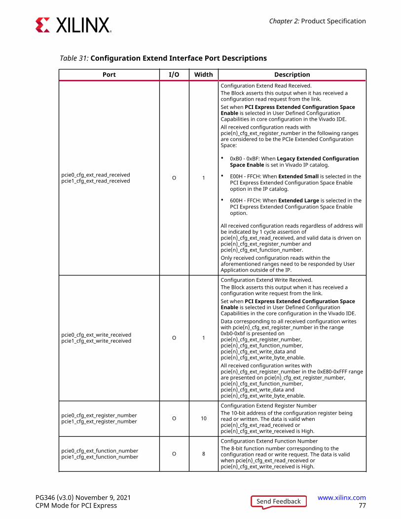
Table 31: Configuration Extend Interface Port Descriptions
Port I/O Width Description
pcie0_cfg_ext_read_receivedpcie1_cfg_ext_read_received O 1
Configuration Extend Read Received.The Block asserts this output when it has received aconfiguration read request from the link.Set when PCI Express Extended Configuration SpaceEnable is selected in User Defined ConfigurationCapabilities in core configuration in the Vivado IDE.All received configuration reads withpcie(n)_cfg_ext_register_number in the following rangesare considered to be the PCIe Extended ConfigurationSpace:
• 0xB0 - 0xBF: When Legacy Extended ConfigurationSpace Enable is set in Vivado IP catalog.
• E00H - FFCH: When Extended Small is selected in thePCI Express Extended Configuration Space Enableoption in the IP catalog.
• 600H - FFCH: When Extended Large is selected in thePCI Express Extended Configuration Space Enableoption.
All received configuration reads regardless of address willbe indicated by 1 cycle assertion ofpcie(n)_cfg_ext_read_received, and valid data is driven onpcie(n)_cfg_ext_register_number andpcie(n)_cfg_ext_function_number.Only received configuration reads within theaforementioned ranges need to be responded by UserApplication outside of the IP.
pcie0_cfg_ext_write_receivedpcie1_cfg_ext_write_received O 1
Configuration Extend Write Received.The Block asserts this output when it has received aconfiguration write request from the link.Set when PCI Express Extended Configuration SpaceEnable is selected in User Defined ConfigurationCapabilities in the core configuration in the Vivado IDE.Data corresponding to all received configuration writeswith pcie(n)_cfg_ext_register_number in the range0xb0-0xbf is presented onpcie(n)_cfg_ext_register_number,pcie(n)_cfg_ext_function_number,pcie(n)_cfg_ext_write_data andpcie(n)_cfg_ext_write_byte_enable.All received configuration writes withpcie(n)_cfg_ext_register_number in the 0xE80-0xFFF rangeare presented on pcie(n)_cfg_ext_register_number,pcie(n)_cfg_ext_function_number,pcie(n)_cfg_ext_wrte_data andpcie(n)_cfg_ext_write_byte_enable.
pcie0_cfg_ext_register_numberpcie1_cfg_ext_register_number O 10
Configuration Extend Register NumberThe 10-bit address of the configuration register beingread or written. The data is valid whenpcie(n)_cfg_ext_read_received orpcie(n)_cfg_ext_write_received is High.
pcie0_cfg_ext_function_numberpcie1_cfg_ext_function_number O 8
Configuration Extend Function NumberThe 8-bit function number corresponding to theconfiguration read or write request. The data is validwhen pcie(n)_cfg_ext_read_received orpcie(n)_cfg_ext_write_received is High.
Chapter 2: Product Specification
PG346 (v3.0) November 9, 2021 www.xilinx.comCPM Mode for PCI Express 77Send Feedback

Table 31: Configuration Extend Interface Port Descriptions (cont'd)
Port I/O Width Description
pcie0_cfg_ext_write_datapcie1_cfg_ext_write_data O 32
Configuration Extend Write DataData being written into a configuration register. Thisoutput is valid when pcie(n)_cfg_ext_write_received isHigh.
pcie0_cfg_ext_write_byte_enablepcie1_cfg_ext_write_byte_enable O 4 Configuration Extend Write Byte Enable
Byte enables for a configuration write transaction.
pcie0_cfg_ext_read_datapcie1_cfg_ext_read_data I 32
Configuration Extend Read DataYou can provide data from an externally implementedconfiguration register to the core through this bus. Thecore samples this data on the next positive edge of theclock after it sets pcie(n)_cfg_ext_read_received High, ifyou have set pcie(n)_cfg_ext_read_data_valid.
pcie0_cfg_ext_read_data_validpcie1_cfg_ext_read_data_valid I 1
Configuration Extend Read Data ValidThe user application asserts this input to the core tosupply data from an externally implementedconfiguration register. The core samples this input dataon the next positive edge of the clock after it setspcie(n)_cfg_ext_read_received High. The core expects theassertions of this signal within 262144 ('h4_0000) clockcycles of user clock after receiving the read request onpcie(n)_cfg_ext_read_received signal. If no response isreceived by this time, the core will send auto-responsewith 'h0 payload, and the user application must discardthe response and terminate that particular requestimmediately.
Configuration VC1 Status InterfaceThe Configuration VC1 Status interface is used to determine the VC1 enablement or disablementby the software, and determine the VC1 resource status.
Note: *cfg_vc1* ports are applicable only for PCIe Controller 0.
Table 32: Configuration VC1 Status Interface Port Descriptions
Port I/O Width Description
pcie0_cfg_vc1_enable O 1
Configuration VC1 Enable: VC1 Resource ControlRegister:VC Enable bit.When 1b, indicates software has enabled VC1 operation.When 0b, indicates that VC1 is disabled by software.
pcie0_cfg_vc1_negotiation_pending O 1
Configuation VC1 Negotiation Pending: VC1 ResourceStatus Register: VC Negotiation Pending bit.When 1b, indicates VC1 negotiation (initialization ordisabling) is in pending state.
Configuration PASID InterfaceThe Configuration PASID interface is used to determine the enablement of the PASID perfunction status by the software.
Chapter 2: Product Specification
PG346 (v3.0) November 9, 2021 www.xilinx.comCPM Mode for PCI Express 78Send Feedback

Note: The pcie0* signals map to PCIe Controller 0 and pcie1* signals map to PCIe Controller 1 in theport descriptions below.
Table 33: Configuration PASID Interface Port Descriptions
Port I/O Width Description
pcie0_cfg_pasid_enablepcie1_cfg_pasid_enable
O 4 Configuation PASID Enable: Per Function PASIDEnable.
pcie0_cfg_pasid_exec_permission_enablepcie1_cfg_pasid_exec_permission_enable
O 4 Configuation PASID Exec Permission Enable: PerFunction PASID Exec Permission Enable.
pcie0_cfg_pasid_privil_mode_enablepcie1_cfg_pasid_privil_mode_enable
O 4 Configuation PASID Privil Mode Enable: Per FunctionPASID Privil Mode Enable.
Ports Not Available in PCIe Controller 1The following output ports are not available in the PCIe Controller 1. A similarly named port isavailable only for the PCIe Controller 0 (starting with pcie0_).
• pcie1_cfg_max_payload
• pcie1_cfg_max_read_req
• pcie1_cfg_function_status
• pcie1_cfg_function_power_state
• pcie1_cfg_rcb_status
• pcie1_cfg_atomic_requester_enable
• pcie1_cfg_10b_tag_requester_enable
• pcie1_cfg_ext_tag_enable
• pcie1_cfg_vc1_enable
• pcie1_cfg_vc1_negotiation_pending
• pcie1_cfg_msg_received
• pcie1_cfg_msg_received_data
• pcie1_cfg_msg_received_type
• pcie1_cfg_msg_transmit_done
• pcie1_cfg_fc_cplh
• pcie1_cfg_fc_cplh_scale
• pcie1_cfg_fc_cpld
• pcie1_cfg_fc_cpld_scale
• pcie1_cfg_flr_in_process
Chapter 2: Product Specification
PG346 (v3.0) November 9, 2021 www.xilinx.comCPM Mode for PCI Express 79Send Feedback
• pcie1_cfg_interrupt_msi_enable
• pcie1_cfg_interrupt_msi_sent
• pcie1_cfg_interrupt_msi_fail
• pcie1_cfg_interrupt_msi_mmenable
• pcie1_cfg_interrupt_msi_mask_update
• pcie1_cfg_interrupt_msi_data
• pcie1_cfg_interrupt_msix_enable
• pcie1_cfg_interrupt_msix_mask
• pcie1_cfg_interrupt_msix_vec_pending_status
Register SpaceThe configuration space is a register space defined by the PCI Express Base Specification 4.0(https://www.pcisig.com/specifications). The Versal® ACAP CPM Mode for PCIe supports Xilinxproprietary read/write configuration interfaces into this register space, and supports up to fourPhysical Functions (PFs) and 252 Virtual Functions (VFs).
The PCI configuration space consists of the following primary parts.
Legacy PCI v4.0 Type 0/1 Configuration Space Header
• Type 0 Configuration Space Header supported for Endpoint configuration
• Type 1 Configuration Space Header supported for Root, Switch Port configuration
Legacy Extended Capability Items
• PCIe Capability
• Power Management Capability
• Message Signaled Interrupt (MSI) Capability
• MSI-X Capability
• Legacy Extend Capabilities
PCIe Extended Capabilities
• Advanced Error Reporting Capability
• Function Level Reset
• ASPM L1 Support
Chapter 2: Product Specification
PG346 (v3.0) November 9, 2021 www.xilinx.comCPM Mode for PCI Express 80Send Feedback

• ASPM L0s Support (supported in Gen1 and Gen2 configurations only)
• Device Serial Number Capability
• Virtual Channel Capability
• ARI Capability (optional)
• SR-IOV Extended Capability Structure
• Configuration Space Extend Capabilities
• Address Translation Services (ATS)
• Page Request Interface (PRI)
• Feature DLLP
• CCIX Transport DVSEC through configuration space extension
• CCIX Protocol DVSEC through configuration space extension
• Transaction Tag Scaling as Requester and Completer
• Flow Control Scaling
• MCAP Interface for Staged Configuration and Dynamic Function eXchange per PCI Expressport
• PASID Capability
• Lane Margining at the Receiver Capability
• Physical Layer 16 GT/s Capability
Chapter 2: Product Specification
PG346 (v3.0) November 9, 2021 www.xilinx.comCPM Mode for PCI Express 81Send Feedback

Chapter 3
Designing with the CoreThis section includes guidelines and additional information to facilitate designing with the core.
ClockingNote: USER_CLK (user_clk) in this section refers to pcie(n)_user_clk, which is also described in theClock and Reset Interface section.
The CPM requires a 100, 125, or 250 MHz reference clock input. The following figure shows theclocking architecture. The user_clk clock can be used as the system clock.
Figure 6: USER_CLK Clocking Architecture
CPM DPLL USER_CLKBUFG_GT
X22710-071520
All user interface signals are timed with respect to the same clock (user_clk) which can have afrequency of 62.5, 125, or 250 MHz depending on the configured link speed and width. Theuser_clk should be used to interface with the CPM. With the user logic, any available clockscan be used.
Each link partner device shares the same reference clock source. The following figures show asystem using a 100 MHz reference clock. Even if the device is part of an embedded system, if thesystem uses commercial PCI Express® root complexes or switches along with typicalmotherboard clocking schemes, synchronous clocking should be used.
Note: The following figures are high-level representations of the board layout. Ensure that coupling,termination, and details are correct when laying out a board.
Chapter 3: Designing with the Core
PG346 (v3.0) November 9, 2021 www.xilinx.comCPM Mode for PCI Express 82Send Feedback
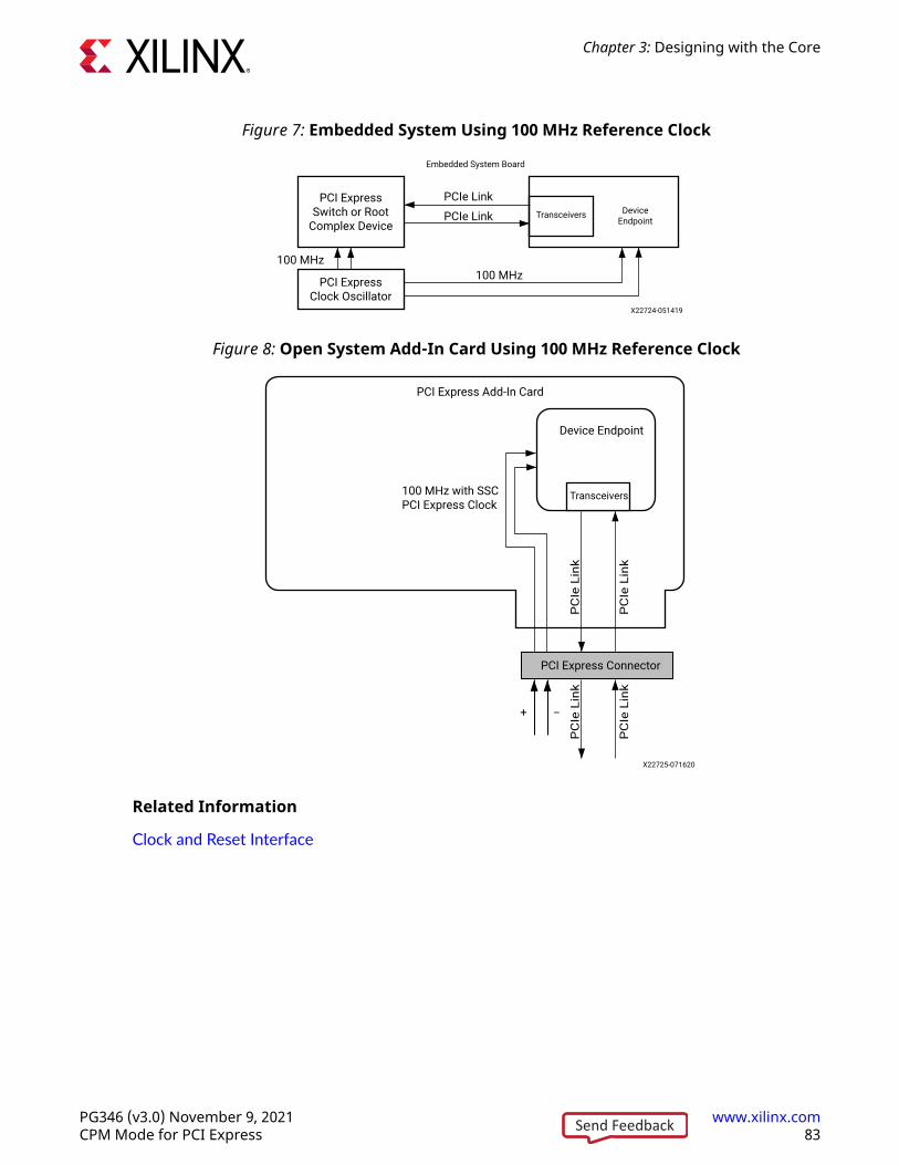
Figure 7: Embedded System Using 100 MHz Reference Clock
DeviceEndpoint
PCI Express Switch or Root
Complex Device
PCI Express Clock Oscillator
100 MHz
Transceivers
100 MHz
Embedded System Board
PCIe Link
PCIe Link
X22724-051419
Figure 8: Open System Add-In Card Using 100 MHz Reference Clock
PC
Ie L
ink
PCI Express Connector
Device Endpoint
Transceivers100 MHz with SSCPCI Express Clock
PCI Express Add-In Card
+ _
PC
Ie L
ink
PC
Ie L
ink
PC
Ie L
ink
X22725-071620
Related Information
Clock and Reset Interface
Chapter 3: Designing with the Core
PG346 (v3.0) November 9, 2021 www.xilinx.comCPM Mode for PCI Express 83Send Feedback

ResetsThe fundamental resets for the CPM PCIe® controllers and associated GTs are perst0n andperst1n. The resets are driven by the I/O inside the PS. In addition, there is a power-on-resetfor CPM driven by the platform management controller (PMC). When both PS and the power-onreset from PMC are released, CPM PCIe controllers and the associated GTs will come out ofreset.
After the reset is released, the core attempts to link train and resumes normal operation.
In addition, there is a pcie(n)_user_reset given from the CPM PCIe controller to the userdesign present in the fabric logic. Whenever CPM PCIe controller goes through a reset, or thereis a link down, the CPM PCIe controller issues a pcie(n)_user_reset to the user design inthe programmable logic (PL) region. After the PCIe link is up, pcie(n)_user_reset is releasedfor the user design to come out of reset.
Tandem ConfigurationOverviewPCI Express® is a plug-and-play protocol, meaning that at power up the PCIe® host willenumerate the system. This process consists of the host enumerating PCIe devices and assigningthem base addresses. As such, PCIe interfaces must be ready when the host queries them or theywill not get assigned a base address. The PCI Express specification states that PERST# candeassert 100 ms after the power good of the systems has occurred, and a PCI Express port mustbe ready to link train 20 ms after PERST# has deasserted. This is commonly referred to as the100 ms boot time requirement, even though 120 ms is the fundamental goal.
Xilinx devices can meet this 120 ms link training requirement by using Tandem Configuration, asolution that splits the programming image into two stages. The first stage quickly configures thePCIe endpoint(s) so the endpoint is ready for link training within 120 ms. The second stage thenconfigures the rest of the device. Two variants are supported:
• Tandem PROM: Loads both stages from a single programming image from a standard primaryboot interface.
• Tandem PCIe: Loads the first stage from a primary boot interface, then the second stage isdelivered via one of the CPM PCIe controllers.
Chapter 3: Designing with the Core
PG346 (v3.0) November 9, 2021 www.xilinx.comCPM Mode for PCI Express 84Send Feedback

Within Xilinx Versal® ACAP, the CPM consists of two PCIe controllers, DMA features, CCIXfeatures, and network on chip (NoC) integration. The Versal® ACAP CPM Mode for PCI Expressenables direct access to the two high-performance, independently customizable PCIe controllers.You can select to have one or both of these controllers enumerate within 120 ms using TandemConfiguration.
While the term Tandem Configuration has been carried forward from prior iterations of thistechnology applied in 7 series, UltraScale™, and UltraScale+™ silicon, the solution isfundamentally different in Versal given how the PCIe controllers are built and configured. Noprogrammable logic is needed to activate an endpoint, so only CPM, XPIPE, NoC, and GTYresources are included along with the PMC in the first stage.
IMPORTANT! Only production Versal silicon is supported for Tandem Configuration. Do NOT use thissolution on engineering silicon (ES1).
Enable the Tandem Configuration SolutionStarting with Vivado 2021.1, an option in the CIPS customization GUI allows you to pick whichoption suits their needs. In the CPM options, a Tandem Configuration selection will be enabledwhen a PCIe Endpoint is selected for PCIe Controller 0 or Controller 1. The three availableoptions are:
• Tandem PROM
• Tandem PCIe
• None
Chapter 3: Designing with the Core
PG346 (v3.0) November 9, 2021 www.xilinx.comCPM Mode for PCI Express 85Send Feedback
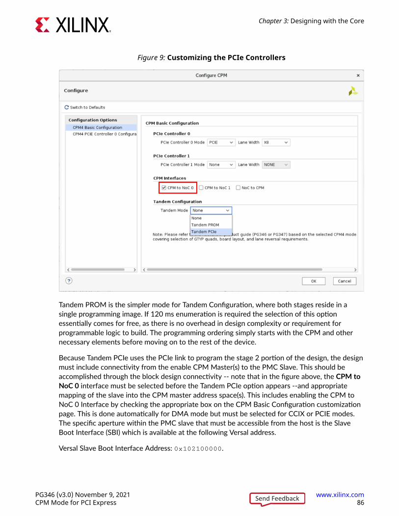
Figure 9: Customizing the PCIe Controllers
Tandem PROM is the simpler mode for Tandem Configuration, where both stages reside in asingle programming image. If 120 ms enumeration is required the selection of this optionessentially comes for free, as there is no overhead in design complexity or requirement forprogrammable logic to build. The programming ordering simply starts with the CPM and othernecessary elements before moving on to the rest of the device.
Because Tandem PCIe uses the PCIe link to program the stage 2 portion of the design, the designmust include connectivity from the enable CPM Master(s) to the PMC Slave. This should beaccomplished through the block design connectivity -- note that in the figure above, the CPM toNoC 0 interface must be selected before the Tandem PCIe option appears --and appropriatemapping of the slave into the CPM master address space(s). This includes enabling the CPM toNoC 0 Interface by checking the appropriate box on the CPM Basic Configuration customizationpage. This is done automatically for DMA mode but must be selected for CCIX or PCIE modes.The specific aperture within the PMC slave that must be accessible from the host is the SlaveBoot Interface (SBI) which is available at the following Versal address.
Versal Slave Boot Interface Address: 0x102100000.
Chapter 3: Designing with the Core
PG346 (v3.0) November 9, 2021 www.xilinx.comCPM Mode for PCI Express 86Send Feedback
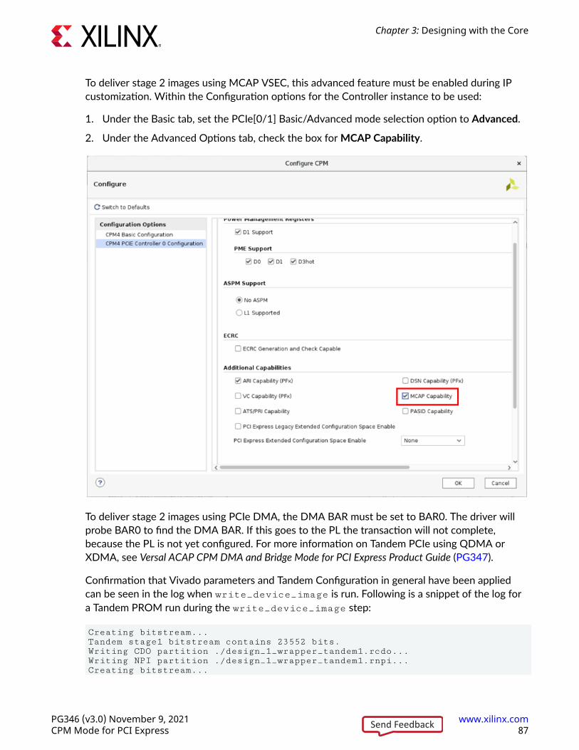
To deliver stage 2 images using MCAP VSEC, this advanced feature must be enabled during IPcustomization. Within the Configuration options for the Controller instance to be used:
1. Under the Basic tab, set the PCIe[0/1] Basic/Advanced mode selection option to Advanced.
2. Under the Advanced Options tab, check the box for MCAP Capability.
To deliver stage 2 images using PCIe DMA, the DMA BAR must be set to BAR0. The driver willprobe BAR0 to find the DMA BAR. If this goes to the PL the transaction will not complete,because the PL is not yet configured. For more information on Tandem PCIe using QDMA orXDMA, see Versal ACAP CPM DMA and Bridge Mode for PCI Express Product Guide (PG347).
Confirmation that Vivado parameters and Tandem Configuration in general have been appliedcan be seen in the log when write_device_image is run. Following is a snippet of the log fora Tandem PROM run during the write_device_image step:
Creating bitstream...Tandem stage1 bitstream contains 23552 bits.Writing CDO partition ./design_1_wrapper_tandem1.rcdo...Writing NPI partition ./design_1_wrapper_tandem1.rnpi...Creating bitstream...
Chapter 3: Designing with the Core
PG346 (v3.0) November 9, 2021 www.xilinx.comCPM Mode for PCI Express 87Send Feedback

Tandem stage2 bitstream contains 5939712 bits.Writing CDO partition ./design_1_wrapper_tandem2.rcdo...Writing NPI partition ./design_1_wrapper_tandem2.rnpi...Writing NPI partition ./design_1_wrapper_shutdown.txt...Generating bif file design_1_wrapper_tandemPROM.bif for Tandem PROM.
The resulting run creates (in addition to the files mentioned above) a single .pdi image for thisdesign called design_1_wrapper.pdi.
When Tandem PCIe is enabled through CIPS IP customization, two .pdi files will be generated:
• tandem1.pdi: This file should be added to the device configuration flash.
• tandem2.pdi: This file should be programmed into the device through the PCIe link once itbecomes active.
The resulting report in the write_device_image log looks nearly identical, but the file namefor the .bif will be slightly different:
Creating bitstream...Tandem stage1 bitstream contains 23552 bits.Writing CDO partition ./design_1_wrapper_tandem1.rcdo...Writing NPI partition ./design_1_wrapper_tandem1.rnpi...Creating bitstream...Tandem stage2 bitstream contains 5939712 bits.Writing CDO partition ./design_1_wrapper_tandem2.rcdo...Writing NPI partition ./design_1_wrapper_tandem2.rnpi...Writing NPI partition ./design_1_wrapper_shutdown.txt...Generating bif file ./design_1_wrapper_tandem1.bif for Tandem stage-1.
In addition to the files mentioned above, the resulting run creates two .pdi images for thisdesign called design_1_wrapper_tandem1.pdi and design_1_wrapper_tandem2.pdi.The _tandem1 and _tandem2 suffixes are automatically added to differentiate the stages.
IMPORTANT! Stage 1 and stage 2 bitstreams must remained paired. While this is trivial for TandemPROM because both stages are stored in a single PDI image, this is a critical consideration for TandemPCIe. If any part of the design is modified such that a full recompilation is triggered, both stage 1 and stage2 images must be updated. Always update both stages when any change is made.
In UltraScale+, the Field Updates solution enables you to build “Reconfigurable Stage Twos”where one could not only pick a stage 2 image from a list of compatible images, but then alsoreconfigure that stage 2 area with another stage 2 image to provide dynamic field updates. InVersal, the first part (for the initial boot of a device) may be supported in the future to allow youto lock a stage 1 image in a small local boot flash; the second part (dynamic reconfiguration) willrequire a Tandem + DFX-based approach to allow for dynamic reconfiguration of a subsection ofthe PL.
For test and debug purposes the HD.TANDEM_BITSTREAMS property can be set on theimplemented design before .pdi file generation to separate a single Tandem PROM .pdi fileinto separate tandem1.pdi and tandem2.pdi files.
set_property HD.TANDEM_BITSTREAMS Separate [current_design]
Chapter 3: Designing with the Core
PG346 (v3.0) November 9, 2021 www.xilinx.comCPM Mode for PCI Express 88Send Feedback
Similarly, the behavior of Tandem PROM or Tandem PCIe file generation can be disabled entirelyby using the HD.TANDEM_BITSTREAMS property on the implemented design before .pdi filegeneration. The following command can be used to do this.
set_property HD.TANDEM_BITSTREAMS NONE [current_design]
Deliver Programming Images to SiliconThe purpose of Tandem Configuration is to be able to program the PCIe endpoint(s) within 120ms before link training starts. The stage 1 file configures the CPM, GTs, and NoC connectionrequired for stage 1 operation. These blocks then become active and can interact with the hostto perform PCIe enumeration.
When using Tandem PROM, configuration of the remainder of the device continues to load fromthe same programming image on the same primary boot device while the PCIe endpoint(s) are upand running. There are no requirements for PERSIST or similar restrictions as was the case withUltraScale+ and prior FPGA architectures.
When using Tandem PCIe, the remainder of the device programming is done by delivering thestage 2 .pdi from the PCIe host as a secondary boot device. There are four data paths in theCPM through which the tandem2.pdi file can be loaded from PCIe into the PMC Slave BootInterface. The specific path you select is determined based on the IP configuration desired foryour specific application. These are enumerated below.
• QDMA MM Data Path: If the QDMA Memory Mapped data path is enabled, it can be used todownload through PCIe into the FPGA Slave Boot Interface at a maximum rate of 3.2Gbytes/s. This is limited by the programming rate of the Slave Boot Interface. Xilinx providessample QDMA drivers and software (see Note below). This data path can only be used withPCIe controller 0 because CPM controller 1 does not support hardened QDMA operation.
• XDMA MM Data Path: If the XDMA Memory Mapped data path is enabled, it can be used todownload through PCIe into the FPGA Slave Boot Interface at a maximum rate of 3.2Gbytes/s. This is limited by the programming rate of the FPGA Slave Boot Interface. Xilinxprovides sample XDMA drivers and software (see Note below). This data path can only beenabled with PCIe controller 0 because CPM controller 1 does not support hardened XDMAoperation.
• AXI Master Bridge: If the AXI Master bridge data path is enabled, it can be used to downloadthrough PCIe into the FPGA Slave Boot Interface at a maximum rate limited by the host’sability to generate PCIe transactions (typically around 700 Mbytes/s for 64-byte transfersfrom the host). Xilinx does not provide sample drivers and software for this because either theXDMA or QDMA data paths are typically enabled with this mode and allow for higher transferrates. This data path can only be enabled with PCIe controller 0 because CPM controller 1does not support hardened AXI Master Bridge operation.
Chapter 3: Designing with the Core
PG346 (v3.0) November 9, 2021 www.xilinx.comCPM Mode for PCI Express 89Send Feedback

• Versal MCAP VSEC: Both controllers in CPM can enable the MCAP Vendor Specific ExtendedCapability. This capability functions differently from UltraScale and UltraScale+ solutions. Itcan be used to download through PCIe into the FPGA Slave Boot Interface at a maximum ratelimited by the host’s ability to generate 32-bit PCIe configuration transactions (typically lowerthan 1 Mbytes/s). This mode of configuration should only be used when the other three datapaths are not available. This includes PCIe Streaming and CCIX modes on either controller.
Note: Xilinx provides sample drivers and software to enable stage 2 programming. These drivers can befound at https://github.com/Xilinx/dma_ip_drivers.
Tandem Configuration PerformanceThe initial programming image is stored in and retrieved from a primary boot device. For TandemPROM, this image contains both stages, and for Tandem PCIe, this image contains only stage 1.To calculate configuration performance, use the stage 1 image size as reported in thewrite_device_image log files (shown above).
When using Tandem PCIe, the stage 2 image is delivered over a secondary boot device.Depending on the delivery path and PCIe controller options, configuration performance can beup to 3.2 GB/s while configuring the programmable logic.
• CPM QDMA-MM to SBI: Gen3x16+ expected bandwidth 3.2 GB/s
• CPM XDMA-MM to SBI: Gen3x16+ expected bandwidth 3.2 GB/s
• CPM AXI-Bridge to SBI: Maximum expected Bandwidth 700 MB/s for 512-bit 64-bytetransfers
• CPM MCAP to SBI: Maximum expected bandwidth 1 MB/s or slower
For more information regarding Versal Configuration and Boot, please consult Versal ACAP SystemSoftware Developers Guide (UG1304).
Design OperationThough the CPM is a hardened integrated block, many features and options that can be selectedduring CIPS configuration will require implementation in programmable soft logic (PL). Any partof the design that has been implemented in the PL will be configured in stage 2. Designconfigurations that require PL resources during PCIe enumeration should not be used withTandem PROM or Tandem PCIe. Specifically, the PCIe extended capability interface should notbe enabled for Tandem modes because these registers are addressed during enumeration and arenot present in the stage 1 portion of the design. Moreover, any other resource in the Versaldevice, such as the R5 or A72 processors in the Scalar Engines, will be programmed after theCPM and its PCI Express endpoint(s). While future enhancements to the Tandem Configurationsolution may open opportunities to quickly booting other dedicated parts of a target device, thecurrent solution focuses exclusively on PCI Express end points in the CPM only for the solepurpose of meeting the 100 ms boot time requirement.
Chapter 3: Designing with the Core
PG346 (v3.0) November 9, 2021 www.xilinx.comCPM Mode for PCI Express 90Send Feedback

Known Issues and Limitations• Engineering Silicon (ES) is not supported for VC1902, VC1802 and VM1802 devices. Onlyproduction silicon is supported for these devices.
• PCIe features incompatible with Tandem Configuration:
○ PCIe Extended Configuration Space, as this requires PL logic.
○ QDMA multi-function is not supported. This feature uses PL mailbox which will be probedduring driver load.
• Stage 1 and stage 2 PDI images must remain linked. If you update one, update the other toensure both stages have been generated from the same implemented design.
• Do not reload the same or a new stage 2 image on the fly. Isolation circuitry on the peripheryof the CPM is designed to ensure safe operation of the PCI Express endpoints prior to the restof the device becoming active. Upon stage 2 completion, this isolation is released and it is notre-enabled for a dynamic reload of the stage 2 image.
• For the Versal architecture, CPM Tandem PROM configuration can be used with postconfiguration flash update. This is different from previous (UltraScale+ and older) architecturesthat did not support Tandem PROM post configuration flash update. Given the lack of dual-mode configuration pins, there is no PERSIST requirement to keep a configuration port active.
• Tandem Configuration is compatible with most Dynamic Function eXchange (DFX) solutions.Care must be taken to keep any DFX Pblock away from the PS-PL boundary where soft logicassociated with the CIPS is placed.
• At this point there is no “Tandem with Field Updates” predefined use case. You can create a“Tandem + DFX” solution noted above where both features are enabled in the same design,but creation of the design hierarchy and floorplan as well as insertion of any decoupling logicare the responsibility of the designer. The dynamic (DFX) portion of the solution would belimited to programmable logic and NoC resources, and not parts of the Scalar Engines(processors).
• The CPM itself (and therefore Tandem Configuration) is not compatible with the Classic SoCBoot flow, which utilizes DFX to separate PS and PL configuration events. This is because theCPM solution requires soft logic for most configurations and thus the DFX region cannot beconstructed to include all of the programmable logic.
Chapter 3: Designing with the Core
PG346 (v3.0) November 9, 2021 www.xilinx.comCPM Mode for PCI Express 91Send Feedback

Chapter 4
Design Flow StepsThis section describes customizing and generating the Versal® ACAP CPM Mode for PCIe,constraining the Versal® ACAP CPM Mode for PCIe, and the simulation, synthesis, andimplementation steps that are specific to this IP Versal® ACAP CPM Mode for PCIe. Moredetailed information about the standard Vivado® design flows and the IP integrator can be foundin the following Vivado Design Suite user guides:
• Vivado Design Suite User Guide: Designing IP Subsystems using IP Integrator (UG994)
• Vivado Design Suite User Guide: Designing with IP (UG896)
• Vivado Design Suite User Guide: Getting Started (UG910)
• Vivado Design Suite User Guide: Logic Simulation (UG900)
Customizing and Generating the CIPS IP CoreThis section includes information about using the Vivado® Design Suite to customize andgenerate the Control, Interfaces and Processing System IP core. This section configures the CIPSIP core to access the CPM PCIe controllers directly. For extended information about the CIPS IPcore, see the Control, Interface and Processing System LogiCORE IP Product Guide (PG352).
Configuring the CIPS IP Core1. In the Vivado IDE, select IP Integrator → Create Block Design from the Flow Navigator, as
shown in the following figure.
Chapter 4: Design Flow Steps
PG346 (v3.0) November 9, 2021 www.xilinx.comCPM Mode for PCI Express 92Send Feedback

A popup dialog displays to create the block design.
2. Click OK. An empty block design diagram canvas opens in the IP integrator.
3. Right-click on the block design canvas and from the context menu select Add IP.
4. Search for cips.
5. Double-click the Control, Interface, and Processing System IP core to customize it.
6. In the Configuration Options pane, leave the settings as default or select appropriate optionsrequired for presets and click Next.
Chapter 4: Design Flow Steps
PG346 (v3.0) November 9, 2021 www.xilinx.comCPM Mode for PCI Express 93Send Feedback

Note: For information about the option presets, see Control, Interface and Processing System LogiCORE IPProduct Guide (PG352).
7. Click the CPM block to configure the core.
Chapter 4: Design Flow Steps
PG346 (v3.0) November 9, 2021 www.xilinx.comCPM Mode for PCI Express 94Send Feedback

The CPM Basic Configuration page displays.
Chapter 4: Design Flow Steps
PG346 (v3.0) November 9, 2021 www.xilinx.comCPM Mode for PCI Express 95Send Feedback

8. Set the PCIe Controller 0 Mode to PCIE, and select the lane width. This setting enables thePCIe Port 0, and in a later step, you will be configuring the PCIe Port 0.
9. If you require the PCIe Port 1, set the PCIe Controller 1 Mode to PCIE, and select the lanewidth.
Table 34: Available Lane Width Combinations
PCIe Port 0 PCIe Port 1X1, X2, X4, or X8 X1, X2, X4, or X8
X16 Not available
Note: There is no PCIe Port 1-only option available.
Note: PCIe Port 1 is available only if the lane width of PCIe Port 0 is less than or equal to X8.
Note: PCIe Port 1 supports up to X8 when PCIe Port 0 is configured up to X8.
Chapter 4: Design Flow Steps
PG346 (v3.0) November 9, 2021 www.xilinx.comCPM Mode for PCI Express 96Send Feedback

10. In the Configuration Options pane, expand CPM4, and click PCIE Controller 0 Configurationto customize the PCIe Port 0 for the Versal ACAP CPM Mode for PCI Express core. It offerstwo modes: Basic, and Advanced. To select a mode, use the CPM Modes drop-down list onthe first page of the Customize IP dialog box. Next section will explain the parametersavailable in each mode.
11. If applicable, in the Configuration Options pane, expand CPM, and click PCIE Controller 1Configuration to customize PCIe Port 1.
12. After configuring the PCIe controller, click OK to return to the Configure screen, as shownbelow.
Chapter 4: Design Flow Steps
PG346 (v3.0) November 9, 2021 www.xilinx.comCPM Mode for PCI Express 97Send Feedback

13. Click PS PMC, and click IO configuration.
The IO Configuration tab has a list of options to configure the external PCIe Reset options.
Chapter 4: Design Flow Steps
PG346 (v3.0) November 9, 2021 www.xilinx.comCPM Mode for PCI Express 98Send Feedback

14. Select the PCIe Reset option located in the Peripheral column.
Notice that the MIO pin selected in the PCIe reset is automatically connected to the PCIereset I/O. In the figure below, MIO 38 is connected to the PCIe reset I/O.
a. For PCIe Port 0 Endpoint configuration: Next to A0 Endpoint, select one of the availableMIOs: PS MIO 18, PMC MIO 24, or PMC MIO 38. This selection should match the MIOthat is connected to the PCIe reset I/O in the board schematic. In the figure below, PMCMIO 38 is selected to correspond to PCIe reset MIO 38.
b. If PCIe Port 1 is enabled: Next to A1 Endpoint, select one of the available MIOs (PS MIO19, PMC MIO 25, or PMC MIO 39) based on which MIO is connected to the PCIe resetI/O in the board schematic.
15. If the board will boot from serial NOR flash, select the a QSPI or OSPI option in Boot Modeoptions to enable programming of the flash on the board. Select the appropriate option basedon availability to match the board schematic.
Chapter 4: Design Flow Steps
PG346 (v3.0) November 9, 2021 www.xilinx.comCPM Mode for PCI Express 99Send Feedback

To set up the boot device, see the Versal ACAP Technical Reference Manual (AM011). If a serialNOR flash boot device will be used, the correct options must be selected to enable thecorrect MIOs.
16. To enable additional I/O interfaces, such as UART, 12C, and USB IOs, select them in thePeripherals section in a similar manner. See the Versal ACAP Technical Reference Manual(AM011) for more details on these interfaces.
Chapter 4: Design Flow Steps
PG346 (v3.0) November 9, 2021 www.xilinx.comCPM Mode for PCI Express 100Send Feedback

Basic Mode ParametersThe Basic mode parameters are explained in this section.
Basic Tab
The following figure shows the initial customization page, used to set the Basic modeparameters.
Chapter 4: Design Flow Steps
PG346 (v3.0) November 9, 2021 www.xilinx.comCPM Mode for PCI Express 101Send Feedback

Figure 10: Basic Tab
• Component Name: Base name of the output files generated for the core. The name mustbegin with a letter and can be composed of these characters: a to z, 0 to 9, and “_.”
• CPM Mode: Allows you to select the Basic or Advanced mode configuration of the core.
• Port Type: Indicates the PCI Express logical device type.
• Maximum Link Speed: The core allows you to select the Maximum Link Speed supported bythe device. Higher link speed cores are capable of training to a lower link speed if connectedto a lower link speed capable device.
• AXI-ST Interface Frequency: Enables you to specify the AXI-ST Interface frequency.
• AXI-ST Interface Width: The core allows you to select the Interface Width. The defaultinterface width set in the Customize IP dialog box is the lowest possible interface width.
• AXI-ST Alignment Mode: When a payload is present, there are two options for aligning thefirst byte of the payload with respect to the datapath. The options are provided to select theCQ/CC and RQ/RC interfaces.
• Enable AXI-ST Frame Straddle: The core provides an option to straddle packets on therequester completion interface when the interface width is 256 bits.
Chapter 4: Design Flow Steps
PG346 (v3.0) November 9, 2021 www.xilinx.comCPM Mode for PCI Express 102Send Feedback
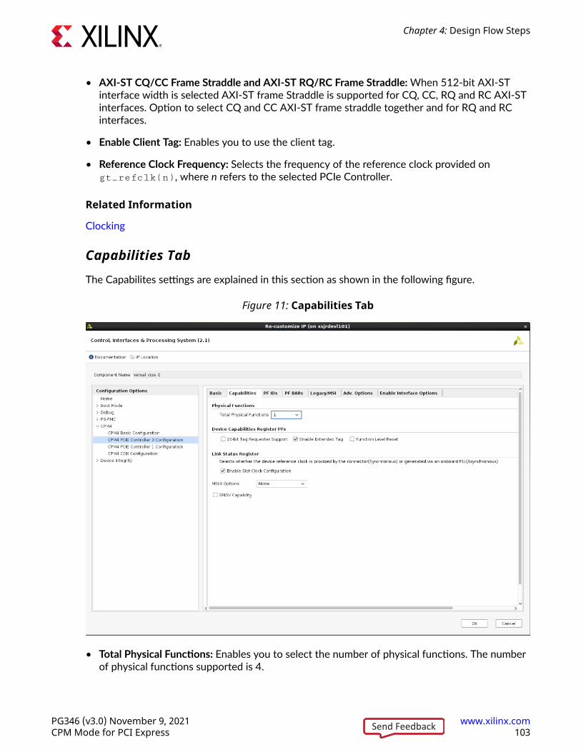
• AXI-ST CQ/CC Frame Straddle and AXI-ST RQ/RC Frame Straddle: When 512-bit AXI-STinterface width is selected AXI-ST frame Straddle is supported for CQ, CC, RQ and RC AXI-STinterfaces. Option to select CQ and CC AXI-ST frame straddle together and for RQ and RCinterfaces.
• Enable Client Tag: Enables you to use the client tag.
• Reference Clock Frequency: Selects the frequency of the reference clock provided ongt_refclk(n), where n refers to the selected PCIe Controller.
Related Information
Clocking
Capabilities Tab
The Capabilites settings are explained in this section as shown in the following figure.
Figure 11: Capabilities Tab
• Total Physical Functions: Enables you to select the number of physical functions. The numberof physical functions supported is 4.
Chapter 4: Design Flow Steps
PG346 (v3.0) November 9, 2021 www.xilinx.comCPM Mode for PCI Express 103Send Feedback
• PFx Max Payload Size: This field indicates the maximum payload size that the device orfunction can support for TLPs. This is the value advertised to the system in the DeviceCapabilities Register.
• Extended Tag Field: This field indicates the maximum supported size of the Tag field. Theoptions are:
• When selected, 8-bit Tag field support (256 tags)
• When deselected, 5-bit Tag field support (32 tags)
• 10-bit Tag Requester Support: This field indicates the maximum supported size of the Tagfield as a Requester. The options are:
• When selected, 10-bit Requester Tag field support (768 tags)
• When deselected, 8-/5-bit Tag supported, depending on Extended Tag Field selection
• Enable Slot Clock Configuration:
Enables the Slot Clock Configuration bit in the Link Status register.
• When this option is selected, the link is synchronously clocked.
• When this option is deselected, asynchronous clock in SRNS mode is supported. SRNSrefers to a separate reference clock with No SSC (an asynchronous clock without SRISsupport).
Related Information
Clocking
PF IDs Tab
The following figure shows the Identity Settings parameters.
Chapter 4: Design Flow Steps
PG346 (v3.0) November 9, 2021 www.xilinx.comCPM Mode for PCI Express 104Send Feedback

Figure 12: PF IDs Tab
• PF0 ID Initial Values:
• Vendor ID: Identifies the manufacturer of the device or application. Valid identifiers areassigned by the PCI Special Interest Group to guarantee that each identifier is unique. Thedefault value, 10EEh, is the Vendor ID for Xilinx. Enter a vendor identification numberhere. FFFFh is reserved.
• Device ID: A unique identifier for the application; the default value depends on theconfiguration selected.
• Revision ID: Indicates the revision of the device or application; an extension of the DeviceID. The default value is 00h; enter a value appropriate for the application.
• Subsystem Vendor ID: Further qualifies the manufacturer of the device or application.Enter a Subsystem Vendor ID here; the default value is 10EEh. Typically, this value is thesame as Vendor ID. Setting the value to 0000h can cause compliance testing issues.
• Subsystem ID: Further qualifies the manufacturer of the device or application. This value istypically the same as the Device ID; the default value depends on the lane width and linkspeed selected. Setting the value to 0000h can cause compliance testing issues.
• Class Code: The Class Code identifies the general function of a device, and is divided intothree byte-size fields:
Chapter 4: Design Flow Steps
PG346 (v3.0) November 9, 2021 www.xilinx.comCPM Mode for PCI Express 105Send Feedback

• Base Class: Broadly identifies the type of function performed by the device.
• Sub-Class: More specifically identifies the device function.
• Interface: Defines a specific register-level programming interface, if any, allowing device-independent software to interface with the device.
Class code encoding can be found at the PCI-SIG website.
• Class Code Look-up Assistant: The Class Code Look-up Assistant provides the Base Class,Sub-Class and Interface values for a selected general function of a device. This Look-upAssistant tool only displays the three values for a selected function. You must enter the valuesin Class Code for these values to be translated into device settings.
PF BARs Tab
The PF BARs tab, shown in the following figure, sets the base address register space for theEndpoint configuration. Each BAR (0 through 5) configures the BAR Aperture Size and Controlattributes of the physical function.
Figure 13: PF BARs Tab Showing PF0 and PF1 Only
Chapter 4: Design Flow Steps
PG346 (v3.0) November 9, 2021 www.xilinx.comCPM Mode for PCI Express 106Send Feedback
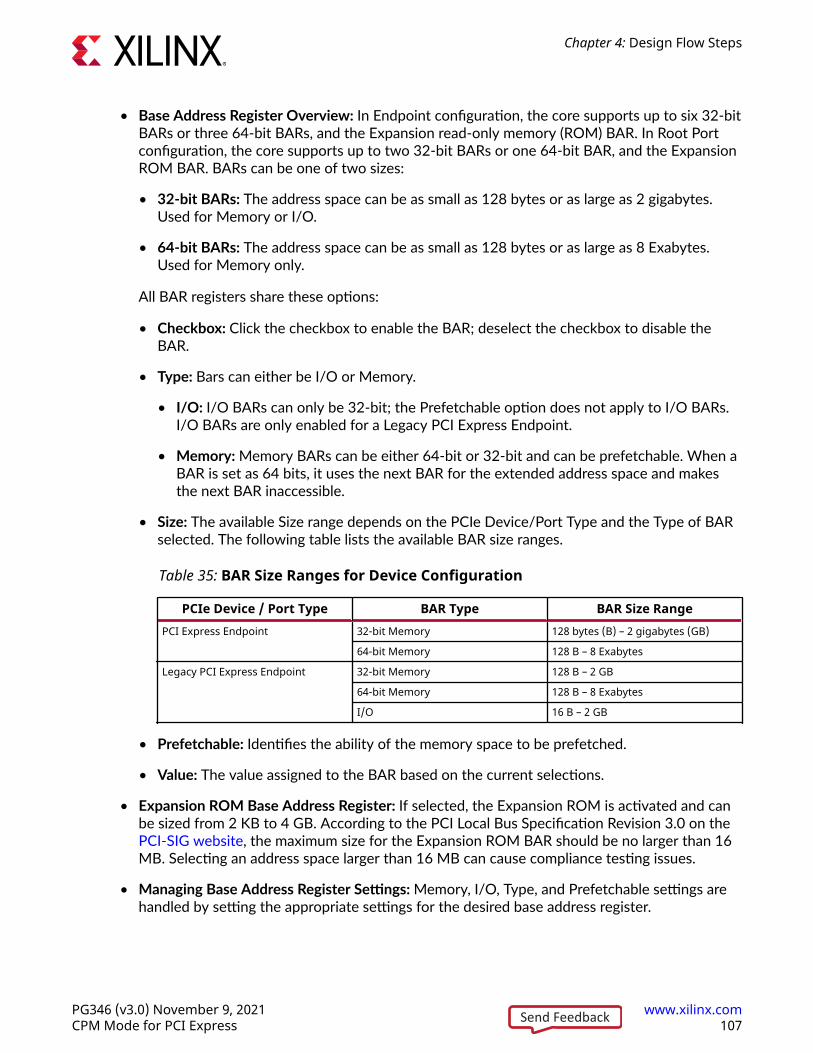
• Base Address Register Overview: In Endpoint configuration, the core supports up to six 32-bitBARs or three 64-bit BARs, and the Expansion read-only memory (ROM) BAR. In Root Portconfiguration, the core supports up to two 32-bit BARs or one 64-bit BAR, and the ExpansionROM BAR. BARs can be one of two sizes:
• 32-bit BARs: The address space can be as small as 128 bytes or as large as 2 gigabytes.Used for Memory or I/O.
• 64-bit BARs: The address space can be as small as 128 bytes or as large as 8 Exabytes.Used for Memory only.
All BAR registers share these options:
• Checkbox: Click the checkbox to enable the BAR; deselect the checkbox to disable theBAR.
• Type: Bars can either be I/O or Memory.
• I/O: I/O BARs can only be 32-bit; the Prefetchable option does not apply to I/O BARs.I/O BARs are only enabled for a Legacy PCI Express Endpoint.
• Memory: Memory BARs can be either 64-bit or 32-bit and can be prefetchable. When aBAR is set as 64 bits, it uses the next BAR for the extended address space and makesthe next BAR inaccessible.
• Size: The available Size range depends on the PCIe Device/Port Type and the Type of BARselected. The following table lists the available BAR size ranges.
Table 35: BAR Size Ranges for Device Configuration
PCIe Device / Port Type BAR Type BAR Size RangePCI Express Endpoint 32-bit Memory 128 bytes (B) – 2 gigabytes (GB)
64-bit Memory 128 B – 8 Exabytes
Legacy PCI Express Endpoint 32-bit Memory 128 B – 2 GB
64-bit Memory 128 B – 8 Exabytes
I/O 16 B – 2 GB
• Prefetchable: Identifies the ability of the memory space to be prefetched.
• Value: The value assigned to the BAR based on the current selections.
• Expansion ROM Base Address Register: If selected, the Expansion ROM is activated and canbe sized from 2 KB to 4 GB. According to the PCI Local Bus Specification Revision 3.0 on the PCI-SIG website, the maximum size for the Expansion ROM BAR should be no larger than 16MB. Selecting an address space larger than 16 MB can cause compliance testing issues.
• Managing Base Address Register Settings: Memory, I/O, Type, and Prefetchable settings arehandled by setting the appropriate settings for the desired base address register.
Chapter 4: Design Flow Steps
PG346 (v3.0) November 9, 2021 www.xilinx.comCPM Mode for PCI Express 107Send Feedback

Memory or I/O settings indicate whether the address space is defined as memory or I/O. Thebase address register only responds to commands that access the specified address space.Generally, memory spaces less than 4 KB in size should be avoided. The minimum I/O spaceallowed is 16 bytes; use of I/O space should be avoided in all new designs.
Prefetchability is the ability of memory space to be prefetched. A memory space isprefetchable if there are no side effects on reads (that is, data is not destroyed by reading, asfrom a RAM). Byte-write operations can be merged into a single double word write, whenapplicable.
When configuring the core as an Endpoint for PCIe (non-Legacy), 64-bit addressing must besupported for all BARs (except BAR5) that have the prefetchable bit set. 32-bit addressing ispermitted for all BARs that do not have the prefetchable bit set. The prefetchable bit-relatedrequirement does not apply to a Legacy Endpoint. The minimum memory address rangesupported by a BAR is 128 bytes for a PCI Express Endpoint and 16 bytes for a Legacy PCIExpress Endpoint.
• Disabling Unused Resources: For best results, disable unused base address registers toconserve system resources. A base address register is disabled by deselecting unused BARs inthe Customize IP dialog box.
• Copy PF0: When set, the Copy PF0 option allows you to set all BARs settings of the remainingPFs to the same values as PF0. Applicable when there are more than one total PhysicalFunction (PF).
Legacy/MSI Cap Tab
On this page, you set the Legacy Interrupt Settings and MSI Capabilities for all applicable physicaland virtual functions. This page is not visible when the SRIOV Capability parameter is selectedon the Capabilities page.
Chapter 4: Design Flow Steps
PG346 (v3.0) November 9, 2021 www.xilinx.comCPM Mode for PCI Express 108Send Feedback
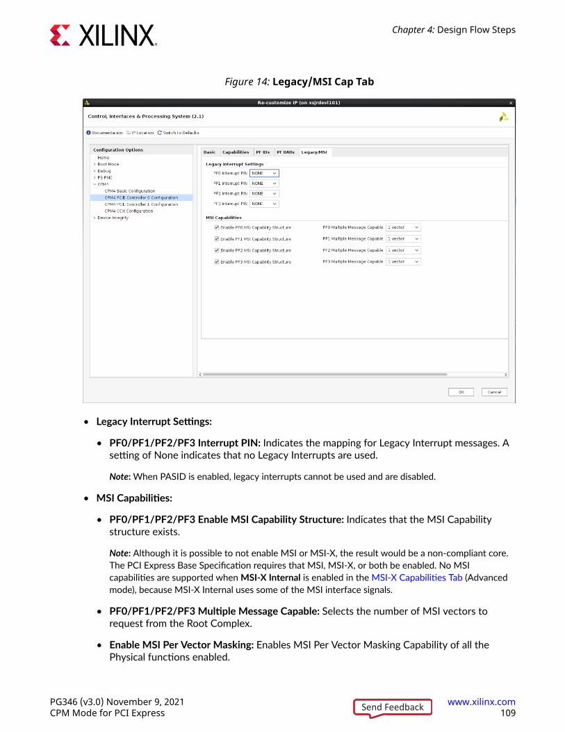
Figure 14: Legacy/MSI Cap Tab
• Legacy Interrupt Settings:
• PF0/PF1/PF2/PF3 Interrupt PIN: Indicates the mapping for Legacy Interrupt messages. Asetting of None indicates that no Legacy Interrupts are used.
Note: When PASID is enabled, legacy interrupts cannot be used and are disabled.
• MSI Capabilities:
• PF0/PF1/PF2/PF3 Enable MSI Capability Structure: Indicates that the MSI Capabilitystructure exists.
Note: Although it is possible to not enable MSI or MSI-X, the result would be a non-compliant core.The PCI Express Base Specification requires that MSI, MSI-X, or both be enabled. No MSIcapabilities are supported when MSI-X Internal is enabled in the MSI-X Capabilities Tab (Advancedmode), because MSI-X Internal uses some of the MSI interface signals.
• PF0/PF1/PF2/PF3 Multiple Message Capable: Selects the number of MSI vectors torequest from the Root Complex.
• Enable MSI Per Vector Masking: Enables MSI Per Vector Masking Capability of all thePhysical functions enabled.
Chapter 4: Design Flow Steps
PG346 (v3.0) November 9, 2021 www.xilinx.comCPM Mode for PCI Express 109Send Feedback

Note: Enabling this option for individual physical functions is not supported.
Advanced Mode ParametersThe following parameters appear on different pages of the IP catalog when Advanced mode isselected for Mode on the Basic page.
Basic Tab
The Basic page with Advanced mode selected (shown in the following figure) includes additionalsettings. The following parameters are visible on the Basic page when the Advanced mode isselected.
Figure 15: Basic Tab, Advanced Mode
• PCIe Link Debug: This enables the link debug option to be activated.
• Enable Lane Reversal: This enables the lane reversal feature.
Chapter 4: Design Flow Steps
PG346 (v3.0) November 9, 2021 www.xilinx.comCPM Mode for PCI Express 110Send Feedback

Capabilities Tab
The Capabilities settings for Advanced mode (as shown in the following figure) contains twoadditional parameters to those for Basic mode and are described below.
Figure 16: Capabilities Tab, Advanced Mode
• Function Level Reset: Enable Function Level Reset (FLR). FLR is supported when the PCIe IP isconfigured as Endpoint.
• SRIOV Capabilities: Enables Single Root Port I/O Virtualization (SR-IOV) capabilities. Theintegrated block implements extended Single Root Port I/O Virtualization PCIe. When this isenabled, SR-IOV is implemented on all the selected physical functions. When SR-IOVcapabilities are enabled MSI support is disabled and you can use MSI-X support as shown inthe above figure.
Note: When SR-IOV capabilities are enabled, MSI support is disabled and you can use MSI-X support.
• MSI-X Options: To enable MSI-X capabilities, select Advanced mode and then select therequired options on the Capabilities tab. There are four options to choose from:
• MSI-X External: In this mode you need to implement MSI-X External interface driving logic,MSI-X Table and PBA buffers outside the PCIe core. You can configure the MSI-X BARs.
Chapter 4: Design Flow Steps
PG346 (v3.0) November 9, 2021 www.xilinx.comCPM Mode for PCI Express 111Send Feedback

• MSI-X Internal: In this mode you need to implement the MSI-X Internal interface drivinglogic only. MSI-X Table and PBA buffers are built into the PCIe core. You can configure theMSI-X BARs.
• MSI-X AXI4-Stream: In this mode user is expected to drive MSI-X interrupts on the AXI4-Stream interface. You can configure the MSI-X BARs.
• None: No MSI-X is supported.
The same MSI-X options are applicable when SRIOV capability is selected.
MSI-X Capabilities Tab
The MSI-X Capabilities parameters, shown in the following figure, are available in Advancedmode only. To enable MSI-X capabilities, select Advanced mode and then select the requiredoptions on the Capabilities page.
The same MSI-X options are applicable when SRIOV capability is selected.
Figure 17: MSI-X Cap Tab, Advanced Mode
• Enable MSI-X Capability Structure: Indicates that the MSI-X Capabilities structure exists.
Chapter 4: Design Flow Steps
PG346 (v3.0) November 9, 2021 www.xilinx.comCPM Mode for PCI Express 112Send Feedback

Note: The Capability Structure needs at least one Memory BAR to be configured. You must maintain theMSI-X Table and Pending Bit Array in the application.
• MSI-X Table Settings: Defines the MSI-X Table structure.
• Table Size: Specifies the MSI-X Table size. Table Size field is expecting N-1 interrupts (0x0Fwill configure a table count of 16).
• Table Offset: Specifies the offset from the Base Address Register that points to the base ofthe MSI-X Table.
• BAR Indicator: Indicates the Base Address Register in the Configuration Space used to mapthe function in the MSI-X Table onto memory space. For a 64-bit Base Address Register,this indicates the lower DWORD.
• MSIx Pending Bit Array (PBA) Settings: Defines the MSI-X Pending Bit Array (PBA) structure.
• PBA Offset: Specifies the offset from the Base Address Register that points to the base ofthe MSI-X PBA.
• PBA BAR Indicator: Indicates the Base Address Register in the Configuration Space used tomap the function in the MSI-X PBA onto Memory Space.
SRIOV Config Tab
The SRIOV Configuration parameters, as shown in the following figure, are described in thissection.
Chapter 4: Design Flow Steps
PG346 (v3.0) November 9, 2021 www.xilinx.comCPM Mode for PCI Express 113Send Feedback
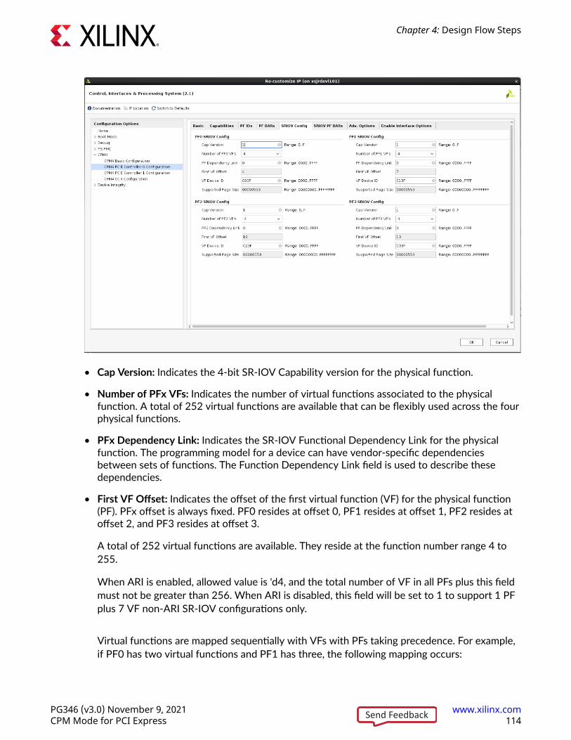
• Cap Version: Indicates the 4-bit SR-IOV Capability version for the physical function.
• Number of PFx VFs: Indicates the number of virtual functions associated to the physicalfunction. A total of 252 virtual functions are available that can be flexibly used across the fourphysical functions.
• PFx Dependency Link: Indicates the SR-IOV Functional Dependency Link for the physicalfunction. The programming model for a device can have vendor-specific dependenciesbetween sets of functions. The Function Dependency Link field is used to describe thesedependencies.
• First VF Offset: Indicates the offset of the first virtual function (VF) for the physical function(PF). PFx offset is always fixed. PF0 resides at offset 0, PF1 resides at offset 1, PF2 resides atoffset 2, and PF3 resides at offset 3.
A total of 252 virtual functions are available. They reside at the function number range 4 to255.
When ARI is enabled, allowed value is 'd4, and the total number of VF in all PFs plus this fieldmust not be greater than 256. When ARI is disabled, this field will be set to 1 to support 1 PFplus 7 VF non-ARI SR-IOV configurations only.
Virtual functions are mapped sequentially with VFs with PFs taking precedence. For example,if PF0 has two virtual functions and PF1 has three, the following mapping occurs:
Chapter 4: Design Flow Steps
PG346 (v3.0) November 9, 2021 www.xilinx.comCPM Mode for PCI Express 114Send Feedback

The PFx_FIRST_VF_OFFSET is calculated by taking the first offset of the virtual function andsubtracting that from the offset of the physical function.
PFx_FIRST_VF_OFFSET = (PFx first VF offset - PFx offset)
In the example above, the following offsets are used:
PF0_FIRST_VF_OFFSET = (4 - 0) = 4PF1_FIRST_VF_OFFSET = (6 - 1) = 5
The initial offset for PF1 is a function of how many VFs are attached to PF0 and is defined inthe following pseudo code:
PF1_FIRST_VF_OFFSET = FIRST_VF_OFFSET + NUM_PF0_VFs - 1
Similarly, for other PFs:
PF2_FIRST_VF_OFFSET = FIRST_VF_OFFSET + NUM_PF0_VFs + NUM_PF1_VFs - 2 PF3_FIRST_VF_OFFSET = FIRST_VF_OFFSET + NUM_PF0_VFs + NUM_PF1_VFs + NUM_PF2_VFs - 3
• VF Device ID: Indicates the 16-bit Device ID for all virtual functions associated with thephysical function.
• SRIOV Supported Page Size: Indicates the page size supported by the physical function. Thisphysical function supports a page size of 2(n+12), if bit n of the 32-bit register is set.
SRIOV PF BARs Tab
The SRIOV Base Address Registers (BARs) set the base address register space for the Endpointconfiguration. Each BAR (0 through 5) configures the SR-IOV BAR aperture size and SR-IOVcontrol attributes.
Chapter 4: Design Flow Steps
PG346 (v3.0) November 9, 2021 www.xilinx.comCPM Mode for PCI Express 115Send Feedback
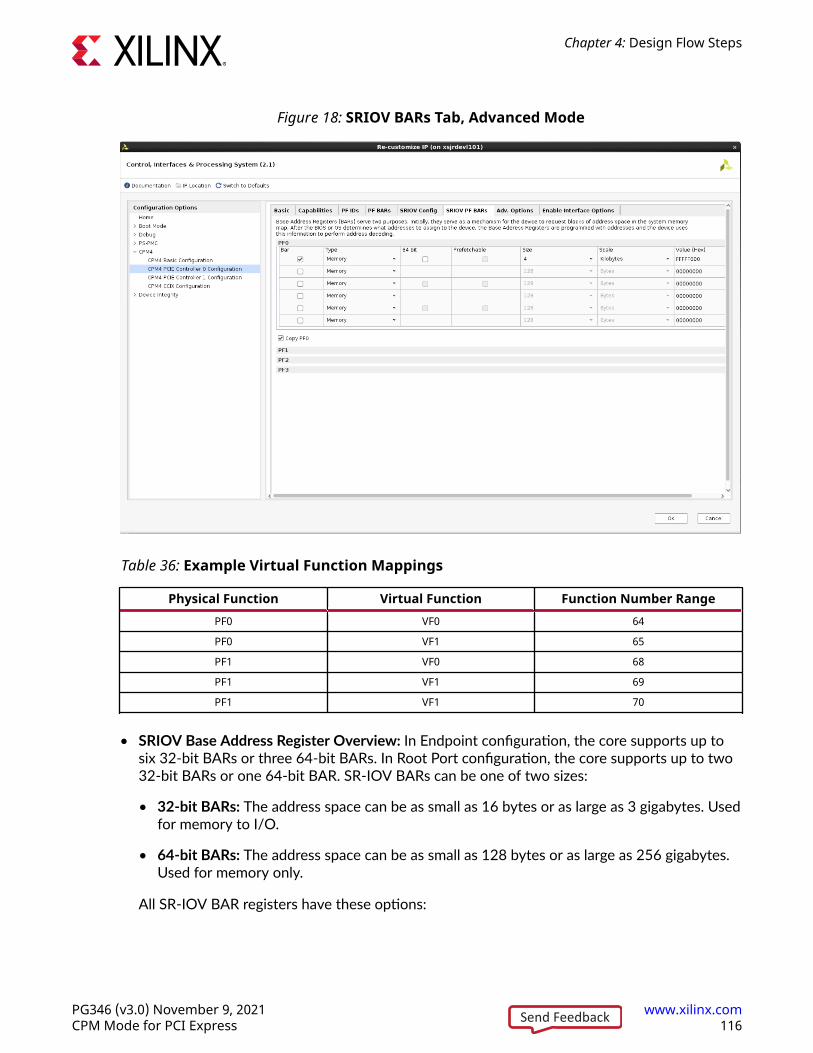
Figure 18: SRIOV BARs Tab, Advanced Mode
Table 36: Example Virtual Function Mappings
Physical Function Virtual Function Function Number RangePF0 VF0 64
PF0 VF1 65
PF1 VF0 68
PF1 VF1 69
PF1 VF1 70
• SRIOV Base Address Register Overview: In Endpoint configuration, the core supports up tosix 32-bit BARs or three 64-bit BARs. In Root Port configuration, the core supports up to two32-bit BARs or one 64-bit BAR. SR-IOV BARs can be one of two sizes:
• 32-bit BARs: The address space can be as small as 16 bytes or as large as 3 gigabytes. Usedfor memory to I/O.
• 64-bit BARs: The address space can be as small as 128 bytes or as large as 256 gigabytes.Used for memory only.
All SR-IOV BAR registers have these options:
Chapter 4: Design Flow Steps
PG346 (v3.0) November 9, 2021 www.xilinx.comCPM Mode for PCI Express 116Send Feedback

• Checkbox: Click the checkbox to enable the BAR; deselect the checkbox to disable theBAR.
• Type: SR-IOV BARs can be either I/O or Memory.
• I/O: I/O BARs can only be 32-bit; the Prefetchable option does not apply to I/O BARs.I/O BARs are only enabled for a Legacy PCI Express Endpoint.
• Memory: Memory BARs can be either 64-bit or 32-bit and can be prefetchable. When aBAR is set to 64-bits, it uses the next BAR for the extended address space and makesthe next BAR inaccessible.
• Size: The available size range depends on the PCIe device/port type and the type of BARselected. The following table lists the available BAR size ranges.
Table 37: SRIOV BAR Size Ranges for Device Configuration
PCIe Device / Port Type BAR Type BAR Size RangePCI Express Endpoint 32-bit Memory 128 bytes – 2 gigabytes
64-bit Memory 128 bytes – 8 exabytes
Legacy PCI Express Endpoint 32-bit Memory 16 bytes – 2 gigabytes
64-bit Memory 16 bytes – 8 exabytes
I/O 16 bytes – 2 gigabytes
• Prefetchable: Identifies the ability of the memory space to be prefetched.
• Value: The value assigned to the BAR based on the current selections.
• Managing SRIOV Base Address Register Settings: Memory, I/O, Type, and Prefetchablesettings are handled by setting the appropriate Customize IP dialog box settings for thedesired base address register.
Memory or I/O settings indicate whether the address space is defined as memory or I/O. Thebase address register only responds to commands that access the specified address space.Generally, memory spaces less than 4 KB in size should be avoided. The minimum I/O spaceallowed is 16 bytes. I/O space should be avoided in all new designs.
A memory space is prefetchable if there are no side effects on reads (that is, data is notdestroyed by reading, as from RAM). Byte-write operations can be merged into a singledouble-word write, when applicable.
When configuring the core as an Endpoint for PCIe (non-Legacy), 64-bit addressing must besupported for all SR-IOV BARs (except BAR5) that have the prefetchable bit set. 32-bitaddressing is permitted for all SR-IOV BARs that do not have the prefetchable bit set. Theprefetchable bit related requirement does not apply to a Legacy Endpoint. The minimummemory address range supported by a BAR is 128 bytes for a PCI Express Endpoint and 16bytes for a Legacy PCI Express Endpoint.
Chapter 4: Design Flow Steps
PG346 (v3.0) November 9, 2021 www.xilinx.comCPM Mode for PCI Express 117Send Feedback

• Disabling Unused Resources: For best results, disable unused base address registers toconserve system resources. Disable base address register by deselecting unused BARs in theCustomize IP dialog box.
• Copy PF0: When set, the Copy PF0 option allows you to set all BAR settings of the remainingPF groups to the same values as PF0 group. Applicable when there are more than one totalPhysical Function (PF).
Adv. Options
The Advanced Options tab enables Power Management Registers and ASPM. There is no L0ssupport when the link speed is not 2.5 GT/s and 5.0 GT/s.
The Advanced Options tab also enables you to choose ECRC check in AER Capability, ARI, DSN,Virtual Channel, MCAP, ATS/PRI, PASID, and PCI Express Extended Config space and PCI LegacyExtended space.
Figure 19: Adv. Options Tab
PCI Express Extended Configuration Space has three options:
Chapter 4: Design Flow Steps
PG346 (v3.0) November 9, 2021 www.xilinx.comCPM Mode for PCI Express 118Send Feedback

• None: No Extended Configuration space required.
• Extended Small: PCI Express Extended space available from 0xE00 - 0xFFC.
• Extended Large: PCI Express Extended space available from 0x600 - 0xFFC.
Interface Parameters
The Interface Parameters tab enables you to enable/disable interfaces that are not required foryour application.
Figure 20: Interface Parameters Tab
Chapter 4: Design Flow Steps
PG346 (v3.0) November 9, 2021 www.xilinx.comCPM Mode for PCI Express 119Send Feedback

Appendix A
GT Selection and Pin Planning forCPM4
This appendix provides guidance on gigabit transceiver (GT) selection for Versal® devices andsome key recommendations that should be considered when selecting the GT locations. The GTlocations for Versal devices can be customized through the IP customization wizard. Thisappendix provides guidance for CPM, PL PCIe® and PHY IP based solutions. In this guide, theCPM related guidance is of primary importance, while the other related guidance might berelevant and is provided for informational purposes.
A GT Quad is comprised of four GT lanes. GT Quad and ref clock locations for CPM4 are in fixedlocations depending on the desired link configuration (see GT Quad Locations). When selectingGT Quads for the PL PCIe-based solution Xilinx® recommends that you use the GT Quad mostadjacent to the integrated block. While this is not required, it will improve place, route, andtiming for the design.
• Link widths of x1, x2, and x4 require one bonded GT Quad and should not split lanes betweentwo GT Quads.
• A link width of x8 requires two adjacent GT Quads that are bonded and are in the same SLR.
• A link width of x16 requires four adjacent GT Quads that are bonded and are in the same SLR.
• PL PCIe blocks should use GTs adjacent to the PCIe block where possible.
• CPM has a fixed connectivity to GTs based on the CPM configuration.
For GTs on the left side of the device, PCIe lane 0 is placed in the bottom-most GT of thebottom-most GT Quad. Subsequent lanes use the next available GTs moving vertically up thedevice as the lane number increments. This means that the highest PCIe lane number uses thetop-most GT in the top-most GT Quad that is used for PCIe.
For GTs on the right side of the device, PCIe lane 0 is placed in the top-most GT of the top-mostGT Quad. Subsequent lanes use the next available GTs moving vertically down the device as thelane number increments. This means that the highest PCIe lane number uses the bottom-mostGT in the bottom-most GT Quad that is used for PCIe.
The PCIe reference clock uses GTREFCLK0 in the PCIe lane 0 GT Quad for x1, x2, x4, and x8configurations. For x16 configurations the PCIe reference clock should use GTREFCLK0 on a GTQuad associated with lanes 8-11. This allows the clock to be forwarded to all 16 PCIe lanes.
Appendix A: GT Selection and Pin Planning for CPM4
PG346 (v3.0) November 9, 2021 www.xilinx.comCPM Mode for PCI Express 120Send Feedback

The PCIe reset pins for CPM designs must connect to one of specified pins for each of the twoPCIe controllers. The PCIe reset pin for PL PCIe and PHY IP designs can be connected to anycompatible PL pin location, or the CPM PCIe reset pins when the corresponding CPM PCIecontroller is not in use. This is summarized in the table below.
Table 38: PCIe Controller Reset Pin Locations
Versal PCIe Controller Versal Reset Pin LocationCPM PCIe Controller 0 PS MIO 18
PMC MIO 24
PMC MIO 38
CPM PCIe Controller 1 PS MIO 19
PMC MIO 25
PMC MIO 39
PL PCIe Controllers Any compatible single-ended PL I/O pin.
Versal ACAP PHY IP Any compatible single-ended PL I/O pin.
CPM4 GT SelectionThe CPM block within Versal devices has a fixed set of GTs that can be used for each of the twoPCIe controllers. These GTs are shared between the two PCIe controllers and High Speed DebugPort (HSDP) as such x16 link widths are only supported when a single PCIe controller is in useand HSDP is disabled. When two CPM PCIe controllers or one PCIe controller and HSDP areenabled each link will be limited to a x8 link width. GT Quad allocation for CPM happens at GTQuad granularity and must include all GT Quads from the most adjacent to the CPM to the top-most GT Quad that is in use by the CPM. GT Quads that are used or between GT Quads that areused by the CPM (for either PCIe or HSDP) cannot be shared with PL resources even if GTswithin the quad are not in use.
CPM in Single Controller Mode
When a single PCIe controller in the CPM is being used and HSDP is disabled, PCIe x1, x2, x4, x8,and x16 link widths are supported. PCIe lane0 is places at the bottom-most GT of the bottom-most GT Quad that is directly above the CPM. Subsequent lanes use the next available GTsmoving vertically up the device as the lane number increments. This means the highest PCIe lanenumber uses the top-most GT in the top-most GT Quad that is used for PCIe. Because the GTlocations and lane ordering for CPM is fixed it cannot be modified through IP customization.
Appendix A: GT Selection and Pin Planning for CPM4
PG346 (v3.0) November 9, 2021 www.xilinx.comCPM Mode for PCI Express 121Send Feedback
As stated previously GT Quad allocation happens at GT Quad granularity and cannot shareunused GT Quad resources with the PL. This means that CPM PCIe controller 0 configurationsthat use x1 or x2 link widths will not use all the GTs within the Quad and that these GTs cannotbe used in the PL for additional GT connectivity. Unused GT Quads in this configuration can beused by the PL to implement PL GT based solutions.
When CPM PCIe controller 0 and High Speed Debug Port (HSDP) is enabled, a PCIe link width ofx16 cannot be used and the CPM will use all three GT Quads that are directly above the CPMregardless of PCIe link width. In this configuration, these GT Quads are allocated to CPM andcannot be shared with PL resources. CPM PCIe lanes 0-7 will be unchanged in their GT selectionand lane ordering. HSDP will use the bottom-most GT that is the third GT Quad away from CPM.This corresponds to the same location as PCIe lane 8 for a x16 link configuration. The fourth GTQuad in this configuration is not use by CPM and can be used to implement PL GT basedsolutions.
CPM in Dual Controller Mode
When the CPM is configured to use two PCIe controllers, High Speed Debug Port (HSDP) cannotbe used because it shares GTs with the two PCIe controllers. Each PCIe controller can support x1,x2, x4 and x8 link widths in this configuration. This configuration will use at least the bottomthree GT Quads closest to the CPM. These GT Quads cannot be used by PL resources. If CPMPCIe controller 1 is using a link width of x1, x2, or x4; then CPM uses three GT Quads. In thiscase the fourth GT Quad can be used by PL resources to implement GT based solutions. If CPMPCIe controller 1 is using a x8 link width, all four GT Quads will be used by the CPM and cannotbe used by PL resources.
CPM PCIe controller 0 lane0 is placed at the bottom-most GT of the bottom-most GT Quad thatis directly above the CPM. Subsequent lanes use the next available GTs moving vertically up thedevice as the lane number increments. CPM PCIe controller 0 lane7 connects to the top-most GTin the second GT Quad away from the CPM.
CPM PCIe controller 1 lane0 is places at the bottom-most GT of third GT Quad above the CPM.Subsequent lanes use the next available GTs moving vertically up the device as the lane numberincrements. CPM PCIe controller 1 lane7 connects to the top-most GT in the fourth GT Quadaway from the CPM.
High Speed Debug Port (HSDP) Only Modes
When the CPM is configured to use the High Speed Debug Port (HSDP) without enabling eitherPCIe controller, the bottom-most GT in the bottom-most GT Quad closest to CPM should beused. This will allow the CPM to use only one GT Quad and allow the next three GT Quads to beused by PL resources.
HSDP can also be enabled for the bottom-most GT in the third GT Quad up from CPM. In thisscenario CPM will use three GT Quads and only use one GT. The remaining unused GTs cannotbe used or shared by PL resources. As result typically HSDP will not be used in this configuration.
Appendix A: GT Selection and Pin Planning for CPM4
PG346 (v3.0) November 9, 2021 www.xilinx.comCPM Mode for PCI Express 122Send Feedback

CPM4 Additional ConsiderationsTo facilitate migration from UltraScale™ or UltraScale+™ designs, boards may be designed to useeither CPM4 or PL PCIe integrated blocks to implement PCIe solutions. When designing a boardto use either CPM4 or the PL PCIe hardblock, the CPM4 pin selection and planning guidelinesshould be followed because they are more restrictive. By doing this a board can be designed thatwill work for either a CPM4 or PL PCIe implementation. To route the PCIe reset from the CPM4to the PL for use with a PL PCIe implementation the following option will need to be enabledunder PS-PMC in the CIPS IP customization GUI.
Figure 21: Configuring the PS PMC
Appendix A: GT Selection and Pin Planning for CPM4
PG346 (v3.0) November 9, 2021 www.xilinx.comCPM Mode for PCI Express 123Send Feedback

When this option is enabled the PCIe reset for each disabled CPM4 PCIe controller will berouted to the PL. The same CPM4 pin selection limitations will apply and the additional PCIereset output pins will be exposed at the boundary of the CIPS IP. If the CPM4 PCIe controller isenabled, the PCIe reset is used internal to the CPM4 and is not routed to the PL for connectivityto PL PCIe controllers.
GT LocationsAssigning GT LocationsUnlike in UltraScale+™ and previous devices implementations where direct assignment of GTs arenot possible in the user constraints, in Versal ACAP implementations the GTs are external to thePCIe® IP and hence the GT assignment can be done in the user constraints. The GT locations areassigned in Quad granularity. (Details of lane 0 placement and lane ordering is found in the GTSelection section. Changing the lane 0 location or lane ordering from the default setting is notsupported. Below is an example of assigning GT locations in a user constraint file.
Note: The gt_quad instances should be assigned contiguously.
set_property LOC GTY_QUAD_X0Y6 [get_cells $gt_quads -filter NAME=~*/gt_quad_3/*]set_property LOC GTY_QUAD_X0Y5 [get_cells $gt_quads -filter NAME=~*/gt_quad_2/*]set_property LOC GTY_QUAD_X0Y4 [get_cells $gt_quads -filter NAME=~*/gt_quad_1/*]set_property LOC GTY_QUAD_X0Y3 [get_cells $gt_quads -filter NAME=~*/gt_quad_0/*]
Related Information
CPM4 GT Selection
GT Quad LocationsThe following table identifies the PCIe lane0 GT Quad(s) that can be used for each PCIecontroller location. The Quad shown in bold is the most adjacent or suggested GT Quad for eachPCIe lane0 location.
Appendix A: GT Selection and Pin Planning for CPM4
PG346 (v3.0) November 9, 2021 www.xilinx.comCPM Mode for PCI Express 124Send Feedback

Table 39: GT Locations
Device Package PCIeBlocks GT QUAD (X16) GT QUAD (X8) GT QUAD (X4
and Below)
XCVC1902 VIVA1596
CPMController 0
GTY_QUAD_X0Y3 GTY_QUAD_X0Y3 GTY_QUAD_X0Y3
CPMController 1
N/A GTY_QUAD_X0Y5 GTY_QUAD_X0Y5
X0Y2 GTY_QUAD_X0Y3GTY_QUAD_X0Y5GTY_QUAD_X0Y4GTY_QUAD_X0Y3
GTY_QUAD_X0Y6GTY_QUAD_X0Y5GTY_QUAD_X0Y4GTY_QUAD_X0Y3
X0Y1 GTY_QUAD_X0Y3GTY_QUAD_X0Y5GTY_QUAD_X0Y4GTY_QUAD_X0Y3
GTY_QUAD_X0Y6GTY_QUAD_X0Y5GTY_QUAD_X0Y4GTY_QUAD_X0Y3
X1Y2 GTY_QUAD_X1Y5GTY_QUAD_X1Y5GTY_QUAD_X1Y4GTY_QUAD_X1Y3
GTY_QUAD_X1Y5GTY_QUAD_X1Y4GTY_QUAD_X1Y3GTY_QUAD_X1Y2
X1Y0 GTY_QUAD_X1Y5GTY_QUAD_X1Y5GTY_QUAD_X1Y4GTY_QUAD_X1Y3
GTY_QUAD_X1Y5GTY_QUAD_X1Y4GTY_QUAD_X1Y3GTY_QUAD_X1Y2
XCVC1902 VSVA2197
CPMController 0 GTY_QUAD_X0Y3 GTY_QUAD_X0Y3 GTY_QUAD_X0Y3
CPMController 1
N/A GTY_QUAD_X0Y5 GTY_QUAD_X0Y5
X0Y2 GTY_QUAD_X0Y3 GTY_QUAD_X0Y5GTY_QUAD_X0Y4GTY_QUAD_X0Y3
GTY_QUAD_X0Y6GTY_QUAD_X0Y5GTY_QUAD_X0Y4GTY_QUAD_X0Y3
X0Y1 GTY_QUAD_X0Y3GTY_QUAD_X0Y5GTY_QUAD_X0Y4GTY_QUAD_X0Y3
GTY_QUAD_X0Y6GTY_QUAD_X0Y5GTY_QUAD_X0Y4GTY_QUAD_X0Y3
X1Y2 GTY_QUAD_X1Y6GTY_QUAD_X1Y6GTY_QUAD_X1Y5GTY_QUAD_X1Y4
GTY_QUAD_X1Y6GTY_QUAD_X1Y5GTY_QUAD_X1Y4GTY_QUAD_X1Y3
X1Y0 GTY_QUAD_X1Y3GTY_QUAD_X1Y3GTY_QUAD_X1Y2GTY_QUAD_X1Y1
GTY_QUAD_X1Y3GTY_QUAD_X1Y2GTY_QUAD_X1Y1GTY_QUAD_X1Y0
Appendix A: GT Selection and Pin Planning for CPM4
PG346 (v3.0) November 9, 2021 www.xilinx.comCPM Mode for PCI Express 125Send Feedback
Table 39: GT Locations (cont'd)
Device Package PCIeBlocks GT QUAD (X16) GT QUAD (X8) GT QUAD (X4
and Below)
XCVC1902 VSVD1760
CPMController 0 GTY_QUAD_X0Y3 GTY_QUAD_X0Y3 GTY_QUAD_X0Y3
CPMController 1
N/A GTY_QUAD_X0Y5 GTY_QUAD_X0Y5
X0Y2 GTY_QUAD_X0Y3 GTY_QUAD_X0Y5GTY_QUAD_X0Y4GTY_QUAD_X0Y3
GTY_QUAD_X0Y6GTY_QUAD_X0Y5GTY_QUAD_X0Y4GTY_QUAD_X0Y3
X0Y1 GTY_QUAD_X0Y3GTY_QUAD_X0Y5GTY_QUAD_X0Y4GTY_QUAD_X0Y3
GTY_QUAD_X0Y6GTY_QUAD_X0Y5GTY_QUAD_X0Y4GTY_QUAD_X0Y3
X1Y2 N/A GTY_QUAD_X1Y4 GTY_QUAD_X1Y4GTY_QUAD_X1Y3
X1Y0 N/A GTY_QUAD_X1Y4 GTY_QUAD_X1Y4GTY_QUAD_X1Y3
XCVM1802 VFVC1760
CPMController 0 GTY_QUAD_X0Y3 GTY_QUAD_X0Y3 GTY_QUAD_X0Y3
CPMController 1
N/A GTY_QUAD_X0Y5 GTY_QUAD_X0Y5
X0Y2 GTY_QUAD_X0Y3 GTY_QUAD_X0Y5GTY_QUAD_X0Y4GTY_QUAD_X0Y3
GTY_QUAD_X0Y6GTY_QUAD_X0Y5GTY_QUAD_X0Y4GTY_QUAD_X0Y3
X0Y1 GTY_QUAD_X0Y3GTY_QUAD_X0Y5GTY_QUAD_X0Y4GTY_QUAD_X0Y3
GTY_QUAD_X0Y6GTY_QUAD_X0Y5GTY_QUAD_X0Y4GTY_QUAD_X0Y3
X1Y2 GTY_QUAD_X1Y6GTY_QUAD_X1Y6GTY_QUAD_X1Y5GTY_QUAD_X1Y4
GTY_QUAD_X1Y6GTY_QUAD_X1Y5GTY_QUAD_X1Y4GTY_QUAD_X1Y3
X1Y0 GTY_QUAD_X1Y3GTY_QUAD_X1Y3GTY_QUAD_X1Y2GTY_QUAD_X1Y1
GTY_QUAD_X1Y3GTY_QUAD_X1Y2GTY_QUAD_X1Y1GTY_QUAD_X1Y0
Appendix A: GT Selection and Pin Planning for CPM4
PG346 (v3.0) November 9, 2021 www.xilinx.comCPM Mode for PCI Express 126Send Feedback

Table 39: GT Locations (cont'd)
Device Package PCIeBlocks GT QUAD (X16) GT QUAD (X8) GT QUAD (X4
and Below)
XCVM1802 VSVA2197
CPMController 0 GTY_QUAD_X0Y3 GTY_QUAD_X0Y3 GTY_QUAD_X0Y3
CPMController 1
N/A GTY_QUAD_X0Y5 GTY_QUAD_X0Y5
X0Y2 GTY_QUAD_X0Y3 GTY_QUAD_X0Y5GTY_QUAD_X0Y4GTY_QUAD_X0Y3
GTY_QUAD_X0Y6GTY_QUAD_X0Y5GTY_QUAD_X0Y4GTY_QUAD_X0Y3
X0Y1 GTY_QUAD_X0Y3GTY_QUAD_X0Y5GTY_QUAD_X0Y4GTY_QUAD_X0Y3
GTY_QUAD_X0Y6GTY_QUAD_X0Y5GTY_QUAD_X0Y4GTY_QUAD_X0Y3
X1Y2 GTY_QUAD_X1Y6GTY_QUAD_X1Y6GTY_QUAD_X1Y5GTY_QUAD_X1Y4
GTY_QUAD_X1Y6GTY_QUAD_X1Y5GTY_QUAD_X1Y4GTY_QUAD_X1Y3
X1Y0 GTY_QUAD_X1Y3GTY_QUAD_X1Y3GTY_QUAD_X1Y2GTY_QUAD_X1Y1
GTY_QUAD_X1Y3GTY_QUAD_X1Y2GTY_QUAD_X1Y1GTY_QUAD_X1Y0
XCVM1802 VSVD1760
CPMController 0 GTY_QUAD_X0Y3 GTY_QUAD_X0Y3 GTY_QUAD_X0Y3
CPMController 1
N/A GTY_QUAD_X0Y5 GTY_QUAD_X0Y5
X0Y2 GTY_QUAD_X0Y3 GTY_QUAD_X0Y5GTY_QUAD_X0Y4GTY_QUAD_X0Y3
GTY_QUAD_X0Y6GTY_QUAD_X0Y5GTY_QUAD_X0Y4GTY_QUAD_X0Y3
X0Y1 GTY_QUAD_X0Y3GTY_QUAD_X0Y5GTY_QUAD_X0Y4GTY_QUAD_X0Y3
GTY_QUAD_X0Y6GTY_QUAD_X0Y5GTY_QUAD_X0Y4GTY_QUAD_X0Y3
X1Y2 N/A GTY_QUAD_X1Y4 GTY_QUAD_X1Y4GTY_QUAD_X1Y3
X1Y0 N/A GTY_QUAD_X1Y4 GTY_QUAD_X1Y4GTY_QUAD_X1Y3
Appendix A: GT Selection and Pin Planning for CPM4
PG346 (v3.0) November 9, 2021 www.xilinx.comCPM Mode for PCI Express 127Send Feedback

Appendix B
DebuggingThis appendix includes details about resources available on the Xilinx® Support website anddebugging tools.
Finding Help on Xilinx.comTo help in the design and debug process when using the Versal® ACAP CPM Mode for PCIe, the Xilinx Support web page contains key resources such as product documentation, release notes,answer records, information about known issues, and links for obtaining further product support.The Xilinx Community Forums are also available where members can learn, participate, share, andask questions about Xilinx solutions.
DocumentationThis product guide is the main document associated with the Versal® ACAP CPM Mode for PCIe.This guide, along with documentation related to all products that aid in the design process, canbe found on the Xilinx Support web page or by using the Xilinx® Documentation Navigator.Download the Xilinx Documentation Navigator from the Downloads page. For more informationabout this tool and the features available, open the online help after installation.
Solution CentersSee the Xilinx Solution Centers for support on devices, software tools, and intellectual propertyat all stages of the design cycle. Topics include design assistance, advisories, and troubleshootingtips.
The Solution Center specific to the Versal® ACAP CPM Mode for PCIe is listed below.
• Xilinx Solution Center for PCI Express
Appendix B: Debugging
PG346 (v3.0) November 9, 2021 www.xilinx.comCPM Mode for PCI Express 128Send Feedback
Answer RecordsAnswer Records include information about commonly encountered problems, helpful informationon how to resolve these problems, and any known issues with a Xilinx product. Answer Recordsare created and maintained daily ensuring that users have access to the most accurateinformation available.
Answer Records for this Versal® ACAP CPM Mode for PCIe can be located by using the SearchSupport box on the main Xilinx support web page. To maximize your search results, use keywordssuch as:
• Product name
• Tool message(s)
• Summary of the issue encountered
A filter search is available after results are returned to further target the results.
Master Answer Record for the Core
AR 73083.
Technical SupportXilinx provides technical support on the Xilinx Community Forums for this LogiCORE™ IP productwhen used as described in the product documentation. Xilinx cannot guarantee timing,functionality, or support if you do any of the following:
• Implement the solution in devices that are not defined in the documentation.
• Customize the solution beyond that allowed in the product documentation.
• Change any section of the design labeled DO NOT MODIFY.
To ask questions, navigate to the Xilinx Community Forums.
PCIe Link Debug EnablementThe Versal® ACAP CPM Mode for PCI Express customization provides an option to enable PCIe®
Link Debug. Enabling this option will insert a debug core inside the IP core that will be recognizedby the Vivado® Hardware Manager and provide PCIe specific debug information and view. Thedebug view provides information relating to the current link speed, current link width, and LTSSMstate transitions, which can facilitate debug of PCIe link related issues.
Appendix B: Debugging
PG346 (v3.0) November 9, 2021 www.xilinx.comCPM Mode for PCI Express 129Send Feedback

Note: This appendix provides guidance for both CPM and PL PCIe based solutions. For this core, the CPMrelated guidance is of primary importance, while the PL PCIe related guidance might be relevant and isprovided for informational purposes.
Enabling PCIe Link DebugUse this guide to enable and connect PCIe Link Debug in a Vivado IP integrator design. Thissection only describes the additional connections that should be added to enable PCIe LinkDebug in a design. It does not discuss how to properly connect the PCIe enabled IPs to create aworking design. Block automation can be used, or the connectivity and connections describedbelow should be added to an existing design and IP configuration.
1. Enable this option in the core customization wizard, and select the options in thecustomization GUI, as shown below. The CPM PCIe cores are customized through the CIPS IPand for PL PCIe cores are customized through the Versal ACAP Integrated Block for PCIe IP.
This adds the PCIe debug core to the PCIe IP and exposes the debug AXI4-Stream interfacesand ports. The debug AXI4-Stream and interface ports should be connected to a Debug HubIP within the Versal design to enable debug for the design. The PCIe example design providesone implementation of how the Debug Hub IP can be connected in Versal designs. This isalso detailed in the description below.
2. Add the Debug Hub IP to the design and use the following configuration options to enablethe Debug Hub AXI Memory Mapped interface along with one set of AXI4-Stream interfaces.Additional AXI4-Stream interfaces can be enabled and connected in your design as desired.
Appendix B: Debugging
PG346 (v3.0) November 9, 2021 www.xilinx.comCPM Mode for PCI Express 130Send Feedback

3. Add the CIPS IP to the design or configure the existing CIPS IP and include the followingconfiguration options. These options will enable an AXI Master, clock, and reset that can beconnected to the Debug Hub IP. To do so:
a. Select PS-PMC → Clock Configuration → Output Clocks → PMC Domain Clocks → PLFabric Clocks selection enable a 100 MHz or similar output clock.
b. Select PS-PMC → PL-PS Interfaces, and enable at least one PL reset in Number of PLResets, and the M_AXI_LPD AXI master.
Appendix B: Debugging
PG346 (v3.0) November 9, 2021 www.xilinx.comCPM Mode for PCI Express 131Send Feedback

4. Add and configure the Processor System Reset IP.
Appendix B: Debugging
PG346 (v3.0) November 9, 2021 www.xilinx.comCPM Mode for PCI Express 132Send Feedback

5. Connect the IPs as shown in the following figures. This may need to be customized to fit withexisting design connectivity.
Appendix B: Debugging
PG346 (v3.0) November 9, 2021 www.xilinx.comCPM Mode for PCI Express 133Send Feedback

After the debug connections have been added to an Vivado IP integrator design, as shownabove, PCIe Link debug is enabled in the generated .pdi image. The connections shown aboveshould be added to a full design and are not sufficient to create a working design alone. The PCIeIP ports and the remainder of the design must be created and configured as per the desiredoperation of the PCIe-enabled IP.
Connecting to PCIe Link Debug in VivadoUse the following steps to connect Viviado Hardware Manager to the FPGA device andassociated PCIe Link Debug enabled design.
1. Open the Hardware Manager.
2. Select the device from the Tools → Program Device… drop-down menu.
3. Select the .pdi and .ltx files for programming the device, and select Program.
Note: You should not load the .ltx file and refresh the target until after the .pdi file has beenprogrammed.
4. Select the PCIe Debug core in the Hardware window. You will see three main views thatinclude the PCIe Debug Core Properties, PCIe Link LTSSM State Trace, and the PCIe LinkLTSSM State Diagram with transitions.
Appendix B: Debugging
PG346 (v3.0) November 9, 2021 www.xilinx.comCPM Mode for PCI Express 134Send Feedback

Using this view, you can observe the active PCIe link status and state transitions. In the PCIeDebug Core Properties window, you can see the name of the PCIe debug core (PCIe_0), thecurrent link status (Gen3x8), and the connected GTs (Quads 103 and 104). The PCIe LTSSM StateTrace view shows a hierarchical view of the PCIe LTSSM state machine transitions. The PCIeLTSSM State Diagram provides a graphical display of the PCIe LTSSM states transitions that weretraversed during the PCIe link up process. Visited LTSSM states are shown in green, the final orcurrent LTSSM state is shown in yellow and the number of times each transition was traversed isidentified on the arcs between states.
In addition to the graphical display, the report_hw_pcie command can be used to generate aconsole text report that contains the PCIe debug information. This information can be sharedwith others to aid in debugging PCIe Link issues. For this example, the name of the debug core isPCIe_0, and is inserted into the command.
report_hw_pcie PCIe_0
This information helps determine where in the PCIe link-up process an issue occurred and canguide further debug of link related issues.
Appendix B: Debugging
PG346 (v3.0) November 9, 2021 www.xilinx.comCPM Mode for PCI Express 135Send Feedback

Appendix C
MigratingThis section provides information for migrating from the UltraScale+™ device PCIe core to the core.
PortsNew Ports
All of the ports in the CPM4 PCIE have pcie0 or pcie1 (as per the core selected ) as prefix tothe port names used in UltraScale+™. For example, for the s_axis_rq_tuser port inUltraScale+ is pcie0_s_axis_rq_tuser in Versal® CPM4.
The following table lists the new ports in the Versal CPM4 Controllers relative to the UltraScale+device integrated block for PCIe IP.
Note: The following tables mentions only pcie0* ports, but apply to both pcie0* and pcie1* ports.
Table 40: New Ports for Versal CPM4
Name I/O Notespcie0_cfg_10b_tag_requester_enable[3:0] O Per function state of Device Control2 Register 10-Bit Tag
Requester Enable bit.
pcie0_cfg_atomic_requester_enable[3:0] O Per function state of Device Control2 Register AtomicOpRequester Enable bit.
pcie0_cfg_ats_control_enable[3:0] O Per function State of ATS Control Register Enable bit.
pcie0_cfg_ext_tag_enable O State of Device Control Register Ext Tag (8-Bit) Enablebit.
pcie0_cfg_fc_vc_sel I Selects the Virtual Channel for the type of flow controlinformation presented on the cfg_fc_* signals.
pcie0_cfg_vc1_enable O VC1 Resource Control Register: VC Enable bit.
pcie0_cfg_vc1_negotiation_pending O VC1 Resource Status Register: VC Negotiation Pendingbit.
pcie0_cfg_pasid_enable[3:0] O Per Function PASID Enable.
pcie0_cfg_pasid_exec_permission_enable[3:0] O Per Function PASID Exec Permission Enable.
pcie0_cfg_pasid_privil_mode_enable[3:0] O Per Function PASID Privil Mode Enable.
pcie0_cfg_fc_ph_scale[1:0] O Please refer to port list for details.
pcie0_cfg_fc_pd_scale[1:0] O Please refer to port list for details.
Appendix C: Migrating
PG346 (v3.0) November 9, 2021 www.xilinx.comCPM Mode for PCI Express 136Send Feedback

Table 40: New Ports for Versal CPM4 (cont'd)
Name I/O Notespcie0_cfg_fc_nph_scale[1:0] O Please refer to port list for details.
pcie0_cfg_fc_npd_scale[1:0] O Please refer to port list for details.
pcie0_cfg_fc_cpld_scale[1:0] O Please refer to port list for details.
pcie0_cfg_fc_cplh_scale[1:0] O Please refer to port list for details.
Port Changes
The following table lists the ports for which the widths were changed in the Versal CPM4Controllers relative to the UltraScale+ device integrated block for PCIe IP.
Table 41: Port Width Changes For Current Ports
Name I/Opcie0_s_axis_rq_tuser[182:0] I
pcie0_s_axis_cq_tuser[228:0] O
pcie0_rq_tag0[9:0] O
pcie0_rq_tag1[9:0] O
Ports Not Available
The following table lists the ports which were deprecated in the Versal CPM4 Controllers relativeto the UltraScale+ device integrated block for PCIe IP.
Table 42: Deprecated Ports
Name I/O Notescfg_pm_aspm_l1_entry_reject I Now part of the register table.
cfg_pm_aspm_tx_l0s_entry_disable I Now part of the register table.
cfg_config_space_enable I Now part of the register table.
cfg_dsn I Now part of the register table.
cfg_dev_id_pf0 I Now part of the register table.
cfg_dev_id_pf1 I Now part of the register table.
cfg_dev_id_pf2 I Now part of the register table.
cfg_dev_id_pf3 I Now part of the register table.
cfg_vend_id I Now part of the register table.
cfg_rev_id_pf0 I Now part of the register table.
cfg_rev_id_pf1 I Now part of the register table.
cfg_rev_id_pf2 I Now part of the register table.
cfg_rev_id_pf3 I Now part of the register table.
cfg_subsys_id_pf0 I Now part of the register table.
cfg_subsys_id_pf1 I Now part of the register table.
Appendix C: Migrating
PG346 (v3.0) November 9, 2021 www.xilinx.comCPM Mode for PCI Express 137Send Feedback
Table 42: Deprecated Ports (cont'd)
Name I/O Notescfg_subsys_id_pf2 I Now part of the register table.
cfg_subsys_id_pf3 I Now part of the register table.
cfg_subsys_vend_id I Now part of the register table.
cfg_ds_port_number I Now part of the register table.
cfg_ds_bus_number I Now part of the register table.
cfg_ds_device_number I Now part of the register table.
cfg_ds_function_number I Now part of the register table.
cfg_link_training_enable I Now part of the register table.
cfg_req_pm_transition_l23_ready I Now part of the register table.
cfg_bus_number I Now part of the register table.
cfg_dpa_substate_change O Not available
cfg_obff_enable O Not available
phy_rdy_out O Not available
sys_reset I Reset now routed via PS.
Related Information
Resets
GT LocationsCPM has a fixed connectivity to GTs based on the CPM configuration. You cannot change the GTlocations in Versal ACAP as was possible in UltraScale+ devices.
Related Information
GT Selection and Pin Planning for CPM4
ClockingCPM4 requires the same reference clock as UltraScale+ devices on the input side. On the outputside, only pcie(n)_user_clk is available for the fabric (user logic). The pcie(n)_user_clksignal can have a frequency of 62.5, 125, or 250 MHz depending on the configured link speedand width.
Appendix C: Migrating
PG346 (v3.0) November 9, 2021 www.xilinx.comCPM Mode for PCI Express 138Send Feedback

Related Information
Clocking
ResetFundamental reset for the PCIe controller is driven by the I/O inside the PS which should beconfigured in CIPS.
Related Information
Resets
FeaturesNew FeaturesPASID
PASID Extended Capability structure has been added which can be enabled via GUI with whichthe core supports sending and receiving TLPs containing a PASID TLP Prefix.
10-Bit Tag
The CPM4 PCIe controller supports 10-bit Tag feature, it inherently supports 10-bit tag on thecompleter interface while requestor interface can be enabled via GUI option. When enabledmanagement of up to 768 tags is possible compared to max of 256 tags in UltraScale+ devices.
Feature DLLP
Data Link Feature Extended Capability structure has been added for link speed of 16.0 GT/s. Itcontains programmable control/status information about the local and peer support of the “DataLink Feature Support”.
Lane Margining
Lane Margining at the Receiver Extended Capability structure has been added for link speed of16.0 GT/s.
Appendix C: Migrating
PG346 (v3.0) November 9, 2021 www.xilinx.comCPM Mode for PCI Express 139Send Feedback

Physical Layer 16.0 GT/s Extended Capability
Physical Layer 16.0 GT/s Extended Capability structure has been added for link speed of 16.0GT/s with which Gen4 equalization status can be read.
Retimers Supported
Link Extension devices (retimers) is supported to interoperate with CPM4 PCIe block for linkspeed of 16.0 GT/s.
Flow Control Informational Select
All combinations of cfg_fc_sel values are supported relative to UltraScale+, refer port descriptionfor more details.
MSIX – Additional Vectors
When configured as MSIX-internal can support up to 32 vectors per physical function comparedto 8 in UltraScale+, vectors per function for VF and total number of vectors (2048) remains thesame.
Switch Mode
CPM4 PCIe controller can be configured as Upstream or Downstream Port of a Switch design.
Features Not Available, or Limited Usage Features• No Example Design - There is no example design support for this release.
• There was a core clock frequency selection available in UltraScale+ for some of theconfigurations which is not available in Versal CPM4.
• Legacy Interrupts cannot be supported when PASID is enabled as some of the ports are re-purposed.
• Pipe mode is currently not supported for Versal CPM4.
• Descrambler is currently not supported for Versal CPM4.
• Some of the advanced GT Settings present in UltraScale+ devices, such as Auto RXEqualization, form factor driver insertion loss adjustment. TX preset selection is not supportedfor Versal CPM4.
• TPH capability is not supported.
Appendix C: Migrating
PG346 (v3.0) November 9, 2021 www.xilinx.comCPM Mode for PCI Express 140Send Feedback

AttributesA complete list of Versal attributes is available in the Versal ACAP Register Reference (AM012).
Appendix C: Migrating
PG346 (v3.0) November 9, 2021 www.xilinx.comCPM Mode for PCI Express 141Send Feedback

Appendix D
Additional Resources and LegalNotices
Xilinx ResourcesFor support resources such as Answers, Documentation, Downloads, and Forums, see XilinxSupport.
Documentation Navigator and Design HubsXilinx® Documentation Navigator (DocNav) provides access to Xilinx documents, videos, andsupport resources, which you can filter and search to find information. To open DocNav:
• From the Vivado® IDE, select Help → Documentation and Tutorials.
• On Windows, select Start → All Programs → Xilinx Design Tools → DocNav.
• At the Linux command prompt, enter docnav.
Xilinx Design Hubs provide links to documentation organized by design tasks and other topics,which you can use to learn key concepts and address frequently asked questions. To access theDesign Hubs:
• In DocNav, click the Design Hubs View tab.
• On the Xilinx website, see the Design Hubs page.
Note: For more information on DocNav, see the Documentation Navigator page on the Xilinx website.
Appendix D: Additional Resources and Legal Notices
PG346 (v3.0) November 9, 2021 www.xilinx.comCPM Mode for PCI Express 142Send Feedback

ReferencesThese documents provide supplemental material useful with this guide:
1. Control, Interface and Processing System LogiCORE IP Product Guide (PG352)
2. Versal ACAP CPM DMA and Bridge Mode for PCI Express Product Guide (PG347)
3. Versal ACAP Integrated Block for PCI Express LogiCORE IP Product Guide (PG343)
4. UltraScale+ Devices Integrated Block for PCI Express LogiCORE IP Product Guide (PG213)
5. Versal ACAP Technical Reference Manual (AM011)
6. Versal ACAP Register Reference (AM012)
7. Versal ACAP CPM CCIX Architecture Manual (AM016)
8. PCI Express Base Specification 4.0 (https://www.pcisig.com/specifications)
9. PCI Express Base Specification 5.0 (https://www.pcisig.com/specifications)
10. Cache Coherent Interconnect for Accelerators (CCIX) Transport Specification (available at http://www.ccixconsortium.com/; membership required).
11. Vivado Design Suite User Guide: Designing IP Subsystems using IP Integrator (UG994)
12. Vivado Design Suite User Guide: Designing with IP (UG896)
13. Versal ACAP System Software Developers Guide (UG1304)
Revision HistoryThe following table shows the revision history for this document.
Section Revision Summary11/09/2021 Version 3.0
General, and Customizing and Generating the CIPS IP Core Updated for CIPS IP version 3.0.
Minimum Device Requirements New information added.
Tandem Configuration New section added, and tandem configuration use casedetails updated throughout.
Limitations New information added.
04/29/2021 Version 2.1
Limitations Added topic to report known issues in the release.
01/08/2021 Version 2.1
Features Updated lane operations.
Appendix D: Additional Resources and Legal Notices
PG346 (v3.0) November 9, 2021 www.xilinx.comCPM Mode for PCI Express 143Send Feedback
Section Revision SummaryPCI Express Endpoint Use Modes Added the Tandem PROM and Tandem PCIe use modes (not
supported in this release).
Port Descriptions Added new section.
Chapter 4: Design Flow Steps Updated with new parameters throughout.
Appendix C: Migrating Added new appendix.
07/24/2020 Version 1.0
Initial Xilinx release. N/A
Please Read: Important Legal NoticesThe information disclosed to you hereunder (the "Materials") is provided solely for the selectionand use of Xilinx products. To the maximum extent permitted by applicable law: (1) Materials aremade available "AS IS" and with all faults, Xilinx hereby DISCLAIMS ALL WARRANTIES ANDCONDITIONS, EXPRESS, IMPLIED, OR STATUTORY, INCLUDING BUT NOT LIMITED TOWARRANTIES OF MERCHANTABILITY, NON-INFRINGEMENT, OR FITNESS FOR ANYPARTICULAR PURPOSE; and (2) Xilinx shall not be liable (whether in contract or tort, includingnegligence, or under any other theory of liability) for any loss or damage of any kind or naturerelated to, arising under, or in connection with, the Materials (including your use of theMaterials), including for any direct, indirect, special, incidental, or consequential loss or damage(including loss of data, profits, goodwill, or any type of loss or damage suffered as a result of anyaction brought by a third party) even if such damage or loss was reasonably foreseeable or Xilinxhad been advised of the possibility of the same. Xilinx assumes no obligation to correct anyerrors contained in the Materials or to notify you of updates to the Materials or to productspecifications. You may not reproduce, modify, distribute, or publicly display the Materialswithout prior written consent. Certain products are subject to the terms and conditions ofXilinx's limited warranty, please refer to Xilinx's Terms of Sale which can be viewed at https://www.xilinx.com/legal.htm#tos; IP cores may be subject to warranty and support terms containedin a license issued to you by Xilinx. Xilinx products are not designed or intended to be fail-safe orfor use in any application requiring fail-safe performance; you assume sole risk and liability foruse of Xilinx products in such critical applications, please refer to Xilinx's Terms of Sale which canbe viewed at https://www.xilinx.com/legal.htm#tos.
AUTOMOTIVE APPLICATIONS DISCLAIMER
AUTOMOTIVE PRODUCTS (IDENTIFIED AS "XA" IN THE PART NUMBER) ARE NOTWARRANTED FOR USE IN THE DEPLOYMENT OF AIRBAGS OR FOR USE IN APPLICATIONSTHAT AFFECT CONTROL OF A VEHICLE ("SAFETY APPLICATION") UNLESS THERE IS ASAFETY CONCEPT OR REDUNDANCY FEATURE CONSISTENT WITH THE ISO 26262AUTOMOTIVE SAFETY STANDARD ("SAFETY DESIGN"). CUSTOMER SHALL, PRIOR TO USING
Appendix D: Additional Resources and Legal Notices
PG346 (v3.0) November 9, 2021 www.xilinx.comCPM Mode for PCI Express 144Send Feedback

OR DISTRIBUTING ANY SYSTEMS THAT INCORPORATE PRODUCTS, THOROUGHLY TESTSUCH SYSTEMS FOR SAFETY PURPOSES. USE OF PRODUCTS IN A SAFETY APPLICATIONWITHOUT A SAFETY DESIGN IS FULLY AT THE RISK OF CUSTOMER, SUBJECT ONLY TOAPPLICABLE LAWS AND REGULATIONS GOVERNING LIMITATIONS ON PRODUCTLIABILITY.
Copyright
© Copyright 2020-2021 Xilinx, Inc. Xilinx, the Xilinx logo, Alveo, Artix, Kintex, Kria, Spartan,Versal, Vitis, Virtex, Vivado, Zynq, and other designated brands included herein are trademarks ofXilinx in the United States and other countries. PCI, PCIe, and PCI Express are trademarks of PCI-SIG and used under license. AMBA, AMBA Designer, Arm, ARM1176JZ-S, CoreSight, Cortex,PrimeCell, Mali, and MPCore are trademarks of Arm Limited in the EU and other countries. Allother trademarks are the property of their respective owners.
Appendix D: Additional Resources and Legal Notices
PG346 (v3.0) November 9, 2021 www.xilinx.comCPM Mode for PCI Express 145Send Feedback