pci express | high speed networks - sg2010 data sheet · 2017-05-30 · a pci-to-pci bridge...
TRANSCRIPT
Dolphin, Inc., 7 Boomhower Rd, Woodsville, NH 03785www.dolphinics.com
SG2010 Data Sheet
Revision Information: 6.3

January 2012
Dolphin, Inc. believes the information in this publication is correct; however, the information is subject to change without notice.
Dolphin, Inc. does not claim that the use of its products in the manner described in this publication will not infringe on any existing or future patent rights, nor do the descriptions contained in this publication imply the granting of licenses to make, use, or sell equipment or software in accordance with the description.
Dolphin, Inc. 2012. All rights reserved.Printed in U.S.A.
Dolphin, StarProtocol, StarFabric, and the Dolphin logo are trademarks of Dolphin, Inc.
All other trademarks and registered trademarks are the property of their respective owners.

January 17, 2012 1
Copy 000
Introduction
Features
2.1 Scalability and Performance . . . . . . . . . . . . . . . . . . . . . . . . . . . . . . . . . . . . . . . . . 2–1
2.2 Compatibility . . . . . . . . . . . . . . . . . . . . . . . . . . . . . . . . . . . . . . . . . . . . . . . . . . . . . . 2–1
2.3 Quality of Service . . . . . . . . . . . . . . . . . . . . . . . . . . . . . . . . . . . . . . . . . . . . . . . . . . 2–1
2.4 Reliability, Availability, Serviceability features . . . . . . . . . . . . . . . . . . . . . . . . . . 2–1
2.5 Advanced Features . . . . . . . . . . . . . . . . . . . . . . . . . . . . . . . . . . . . . . . . . . . . . . . . . 2–2
2.6 Additional features . . . . . . . . . . . . . . . . . . . . . . . . . . . . . . . . . . . . . . . . . . . . . . . . . 2–2
StarFabric Features
3.1 Scalability. . . . . . . . . . . . . . . . . . . . . . . . . . . . . . . . . . . . . . . . . . . . . . . . . . . . . . . . . 3–1
3.2 Component Types . . . . . . . . . . . . . . . . . . . . . . . . . . . . . . . . . . . . . . . . . . . . . . . . . . 3–2
3.3 Routing Methods . . . . . . . . . . . . . . . . . . . . . . . . . . . . . . . . . . . . . . . . . . . . . . . . . . . 3–2
3.4 Traffic Classes . . . . . . . . . . . . . . . . . . . . . . . . . . . . . . . . . . . . . . . . . . . . . . . . . . . . . 3–2
3.5 Fault Tolerant Strategies . . . . . . . . . . . . . . . . . . . . . . . . . . . . . . . . . . . . . . . . . . . . 3–2
3.6 Flow Control. . . . . . . . . . . . . . . . . . . . . . . . . . . . . . . . . . . . . . . . . . . . . . . . . . . . . . . 3–2
3.7 Bandwidth Reservation. . . . . . . . . . . . . . . . . . . . . . . . . . . . . . . . . . . . . . . . . . . . . . 3–3
3.8 Usage Models . . . . . . . . . . . . . . . . . . . . . . . . . . . . . . . . . . . . . . . . . . . . . . . . . . . . . 3–3
Specifications
4.1 Block Diagram . . . . . . . . . . . . . . . . . . . . . . . . . . . . . . . . . . . . . . . . . . . . . . . . . . . . . 4–1
4.2 Usage Models . . . . . . . . . . . . . . . . . . . . . . . . . . . . . . . . . . . . . . . . . . . . . . . . . . . . . 4–24.2.1 Root mode with Bridge function enabled . . . . . . . . . . . . . . . . . . . . . . . . . . . . . . 4–24.2.2 Leaf Mode with Bridge Function enabled . . . . . . . . . . . . . . . . . . . . . . . . . . . . . . 4–34.2.3 Gateway-only usage model . . . . . . . . . . . . . . . . . . . . . . . . . . . . . . . . . . . . . . . . 4–34.2.4 SG2010 Functional Modes . . . . . . . . . . . . . . . . . . . . . . . . . . . . . . . . . . . . . . . . . 4–4
4.3 Package Diagram. . . . . . . . . . . . . . . . . . . . . . . . . . . . . . . . . . . . . . . . . . . . . . . . . . . 4–54.3.1 Pinout Diagram . . . . . . . . . . . . . . . . . . . . . . . . . . . . . . . . . . . . . . . . . . . . . . . . . . 4–6
4.4 Pin List . . . . . . . . . . . . . . . . . . . . . . . . . . . . . . . . . . . . . . . . . . . . . . . . . . . . . . . . . . . 4–74.4.1 Power Pins . . . . . . . . . . . . . . . . . . . . . . . . . . . . . . . . . . . . . . . . . . . . . . . . . . . . 4–12
4.5 Pin Descriptions . . . . . . . . . . . . . . . . . . . . . . . . . . . . . . . . . . . . . . . . . . . . . . . . . . 4–134.5.1 Strapping Pins. . . . . . . . . . . . . . . . . . . . . . . . . . . . . . . . . . . . . . . . . . . . . . . . . . 4–16
4.6 Package Specification. . . . . . . . . . . . . . . . . . . . . . . . . . . . . . . . . . . . . . . . . . . . . . 4–17
Electrical Specifications
5.1 Absolute Maximum Ratings . . . . . . . . . . . . . . . . . . . . . . . . . . . . . . . . . . . . . . . . . . 5–1
5.2 DC Specifications . . . . . . . . . . . . . . . . . . . . . . . . . . . . . . . . . . . . . . . . . . . . . . . . . . 5–1
2 January 17, 2012
Copy 000
5.3 Timing Specifications . . . . . . . . . . . . . . . . . . . . . . . . . . . . . . . . . . . . . . . . . . . . . . . 5–35.3.1 PCI Interface . . . . . . . . . . . . . . . . . . . . . . . . . . . . . . . . . . . . . . . . . . . . . . . . . . . . 5–35.3.2 Parallel and Serial ROM Interface . . . . . . . . . . . . . . . . . . . . . . . . . . . . . . . . . . . 5–45.3.3 Reference ClockTiming. . . . . . . . . . . . . . . . . . . . . . . . . . . . . . . . . . . . . . . . . . . . 5–55.3.4 Global PLL Bypass Clock . . . . . . . . . . . . . . . . . . . . . . . . . . . . . . . . . . . . . . . . . . 5–55.3.5 StarFabric Interface Timing. . . . . . . . . . . . . . . . . . . . . . . . . . . . . . . . . . . . . . . . . 5–55.3.6 JTAG Timing . . . . . . . . . . . . . . . . . . . . . . . . . . . . . . . . . . . . . . . . . . . . . . . . . . . . 5–65.3.7 Asynchronous and Static Signals . . . . . . . . . . . . . . . . . . . . . . . . . . . . . . . . . . . . 5–6
0.1 Internal Pull-up and Pull-down Resistors . . . . . . . . . . . . . . . . . . . . . . . . . . . . . . . 5–7
Industrial Temperature
6.1 Abstract . . . . . . . . . . . . . . . . . . . . . . . . . . . . . . . . . . . . . . . . . . . . . . . . . . . . . . . . . . 6–1
6.2 Clock Details . . . . . . . . . . . . . . . . . . . . . . . . . . . . . . . . . . . . . . . . . . . . . . . . . . . . . . 6–1
6.3 Design Guidelines . . . . . . . . . . . . . . . . . . . . . . . . . . . . . . . . . . . . . . . . . . . . . . . . . . 6–1
Contact Information
7.1 Ordering Information. . . . . . . . . . . . . . . . . . . . . . . . . . . . . . . . . . . . . . . . . . . . . . . . 7–1
7.2 Headquarters . . . . . . . . . . . . . . . . . . . . . . . . . . . . . . . . . . . . . . . . . . . . . . . . . . . . . . 7–1
January 17, 2012 –3
Copy 000
Preface
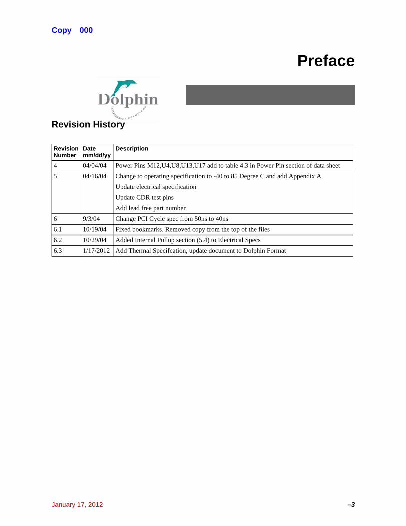
Revision History
RevisionNumber
Datemm/dd/yy
Description
4 04/04/04 Power Pins M12,U4,U8,U13,U17 add to table 4.3 in Power Pin section of data sheet
5 04/16/04 Change to operating specification to -40 to 85 Degree C and add Appendix A
Update electrical specification
Update CDR test pins
Add lead free part number
6 9/3/04 Change PCI Cycle spec from 50ns to 40ns
6.1 10/19/04 Fixed bookmarks. Removed copy from the top of the files
6.2 10/29/04 Added Internal Pullup section (5.4) to Electrical Specs
6.3 1/17/2012 Add Thermal Specifcation, update document to Dolphin Format

Copy 000
–4 January 17, 2012

January 17, 2012 Introduction 1–1
Copy 000
1
Introduction
The StarGen SG2010 is a PCI peripheral chip that bridges StarFabric’s serial interface to PCI devices for communication and embedded systems. The SG2010 expands the capabilities of PCI by providing higher levels of scalability and reliability to PCI based systems, along with the advanced features of StarFabric. Working in conjunction with the SG1010 StarFabric Switch, the SG2010 supports flexible topologies that can be designed to fit specific application bandwidth, reliability, and endpoint or slot require-ments. System designers are able to support next generation system requirements while maintaining their investments in peripherals, applications, and software.
The SG2010 is a multifunction device. Unlike a traditional PCI peripheral, the SG2010 supports both address routing as well as path and multicast routing. A PCI-to-PCI bridge function in the SG2010 supports legacy address routed traffic, which provides 100% compatibility with PCI drivers, application software, BIOS, OSs, configuration code, etc. The interconnect looks like a collection of PCI-to-PCI bridges. The Gateway function of the SG2010 is used to enable the fabric’s advanced features, such as path routing, class of service, bandwidth selection, redundancy for fail-over path routing, and channels. Additional software is necessary to take advantage of these advanced fea-tures. StarGen provides a set of software enablers to minimize this effort. System designers can choose their rate of migration to these advanced features.
In order to shorten design cycles and time to market, the SG2010 employes a well-understood physical layer technology, a serial interconnect with 622Mbps low voltage differential signaling (LVDS). This technology is extensively applied and thoroughly understood by industry professionals. Four transmit and receive differential pairs are used to provide 2.5Gbps full duplex link bandwidth or 5Gbps of total bandwidth per StarFabric link. Unlike some other technologies, designers don’t have to deal with sig-nificant physical interface issues. In conjunction with the SG1010 switch, designs can span from chip-to-chip to room area networks. Designs using inexpensive twisted pair copper cable can work with distances of up to 10 meters. 8B/10B-encoding algorithms allows AC coupling and assists in clock recovery. The PCI interface supports 64-bit or 32-bit PCI buses operating at 66MHz or 33 MHz. A bundled link (two StarFabric links) can support the full bandwidth of a 64bit/66MHz PCI bus.
The SG2010 was designed to work with other StarFabric devices. The StarFabric proto-col integrates both control and data traffic within a single protocol. Most other intercon-nects are designed for either control or data traffic. StarFabric, from its beginning, has been developed to meet the specific requirements of next generation systems.

Copy 000
1–2 Introduction January 17, 2012

January 17, 2012 Features 2–1
Copy 000
2
Features
2.1 Scalability and Performance
• 2 Starfabric links, 2.5 Gbps, full duplex
• Links can be bundled to create a 5.0 Gbps, full duplex point to point link
• 64-bit, 66MHz capable PCI bus
2.2 Compatibility
• Standard PCI-to-PCI addressing support: 100% PCI software compatibility
• Support for PCI transactions plus enhanced capabilities including: write combin-ing, read data retention, and fast back-to-back support
• Compliant with the PCI Local Bus Specification Revision 2.2, the PCI to PCI Bridge Architecture Specification Revision 1.1, and the CompactPCI Hot Swap Specification
• Physical layer interface is compliant with the IEEE 1596.3 and TIA/EIA-644 Low-Voltage Differential Signaling (LVDS) standards.
2.3 Quality of Service
• Support for three routing methods: Standard PCI addressing (address routing), path routing, and multicast routing
• 4 Classes of service: Asynchronous, Isochronous, Multicast, and Provisioning
• Credit based flow control
2.4 Reliability, Availability, Serviceability features
• Link-by-link CRC checking on all traffic
• 8b/10b error correction
• Fault detection and isolation
• Redundant path routing capability, optional automatic fail-over
• Path protection capability for secure operation
• Hot-pluggable links
Advanced Features Copy 000
2–2 Features January 17, 2012
• CPCI Hot Swap support
2.5 Advanced Features
• Advanced event generation and handling
• Prescriptive read support
• Write with acknowledge support
2.6 Additional features
• Supports software generated StarFabric frames
• Supports software generated PCI transactions
• SROM & Flash ROM interfaces for power-up configuration and code pre-load
• LED indicators for each differential pair
• 3.3-V PCI operation with 5.0 tolerant I/O

January 17, 2012 StarFabric Features 3–1
Copy 000
3
StarFabric Features
3.1 Scalability
StarFabric provides a scalable switched interconnect. The SG1010 switch has 30Gbps of switching capacity. When cascaded, the device enables systems to scale to gigabytes per second of capacity. The initial physical layer implemented provides 2.5 Gbps full-duplex bandwidth per link. Two links can be aggregated to create a ‘fat pipe’ with dou-ble the bandwidth. The links are well suited for chip-to-chip, backplane, and rack-to-rack interconnect. Using standard category 5 unshielded copper cables the links can extend to over 10 meters in length enabling the creation of room scale equipment.
Bridge
Bridge
Bridge
Bridge
Switch
Bridge
Bridge

Component Types Copy 000
3–2 StarFabric Features January 17, 2012
3.2 Component Types
The two component types in StarFabric are edge nodes and switches. Switches forward traffic through the StarFabric. Edge nodes provide the connection between the fabric and other protocols or devices. Bridges are edge nodes that translate other protocols (e.g., PCI, H.110) into serial StarFabric traffic. An edge node is further classified into either a root or a leaf. The root initiates fabric resets and enumeration.
3.3 Routing Methods
• Address Routing
– Provides full compatibility with PCI standard
• Path and Multicast routing
– Provides Quality of service, reliability, and high availability
3.4 Traffic Classes
StarFabric supports 7 traffic classes. The initial parts support 4 traffic classes.
• Asynchronous / address routed class
• Isochronous Class
• Multicast Class
• High Priority Class/provisioning
3.5 Fault Tolerant Strategies
• Parallel Fabrics
– A second fabric provides redundancy. Redundant switches are used so that if any switch fails end nodes remain connected. If a particular path fails, packets can be re-routed by silicon or software over the remaining functional paths.
• Fragile links
– Automatic re-striping of data over functioning differential pairs in a link when one to three pairs fail.
3.6 Flow Control
Line credits manage flow control. Line credits counters are used to track available buffer storage between link partners. Each transmission point in the fabric has buffers for each class of traffic for each outgoing port. Traffic is sent only when the source has line credits for the output buffer on the next node for an entire frame. A switch is non-blocking because edge node congestion does not impact traffic flow to any other edge node or even to the same edge node in a different class of service. Line credits are used when a node sends a frame and restored when the node’s link partner forwards the frame.

January 17, 2012 StarFabric Features 3–3
Copy 000 Bandwidth Reservation
3.7 Bandwidth Reservation
Isochronous and multicast transmissions can use bandwidth reservation to allocate anticipated bandwidth requirements prior to starting data transfer. Bandwidth reserva-tion is fully distributed and is initiated at the origin of the traffic.
3.8 Usage Models
Current StarFabric components support 3 usage models, PCI legacy, Fabric-native, and mixed legacy / Fabric-native. PCI legacy enables use of existing PCI drivers and initial-ization software with no modification. the interconnect looks like a collection of PCI-to-PCI bridges. This usage model amounts to a plug-and-play mode that extends the capabilities of existing systems.
The Fabric-native usage unleashes some of StarFabric’s advanced features such as path routing, class of service, bandwidth reservation, redundancy for fail-over path routing, and channels. Fabric-native use also provides the isolation and mechanisms required for inter-processor communication. This enables distributed computing applications. It is possible to use a mixture of legacy and fabric-native capabilities. Developers can start with legacy and add enhanced fabric- native capability over time.
To use advanced features, additional software is necessary. StarGen provides software tools to take advantage of StarFabric’s advanced features. Sample software includes enumeration and routing, bandwidth reservation, as well as routines for optimizing per-formance, API integration layers, BIOS initial setup, and generating statistics. StarGen supplies tools and utilities for ROM programming, fabric access tools, and fabric topol-ogy viewers.

Usage Models Copy 000
3–4 StarFabric Features January 17, 2012
January 17, 2012 Specifications 4–1
Copy 000
4
Specifications
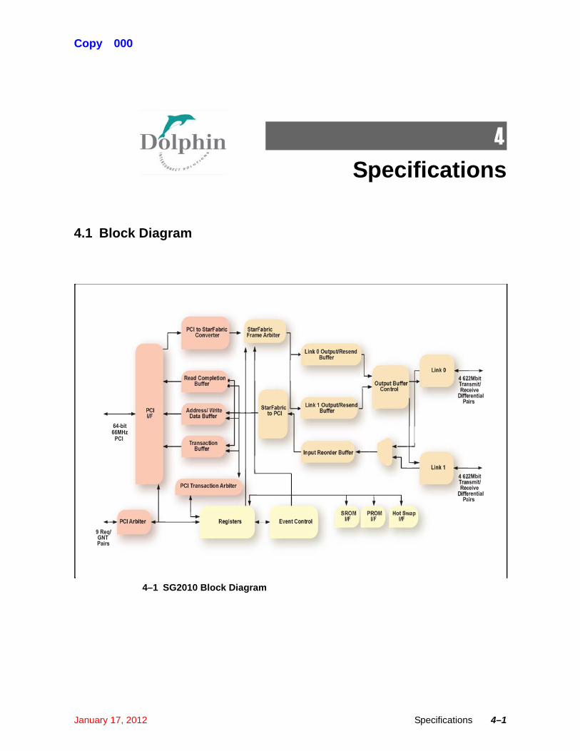
4.1 Block Diagram
4–1 SG2010 Block Diagram
Link 0
Link 1
4 622MbitTransmit/Receive
DifferentialPairs
4 622MbitTransmit/Receive
DifferentialPairs
SROMI/F
PROMI/F
Hot SwapI/FEvent ControlRegisters
PCI Transaction Arbiter
PCI to StarFabricConverter
Read CompletionBuffer
Address/ WriteData Buffer
TransactionBuffer
PCII/F
64-bit66MHz
PCI
PCI Arbiter
9 Req/GNTPairs
Link 0 Output/ResendBuffer
Link 1 Output/ResendBuffer
Input Reorder Buffer
StarFabricFrame Arbiter
StarFabricto PCI
Output BufferControl
Usage Models Copy 000
4–2 Specifications January 17, 2012
4.2 Usage Models
The SG2010 supports two addressing models - a StarFabric addressing model and a PCI addressing model. To support these two addressing models, the SG2010 imple-ments two major functions - a PCI-to-PCI bridge function and a PCI-to-StarFabric Gateway function. The Bridge function supports the PCI addressing model within the fabric and the Gateway function performs translations between the PCI and StarFabric addressing models. The Bridge function can be disabled, but the Gateway function is always present.The SG2010 can be used in one of three basic functional modes:
• Gateway - Root mode, Bridge function is enabled.
• Gateway - Leaf mode, Bridge function is enabled
• Gateway -Bridge function is disabled;
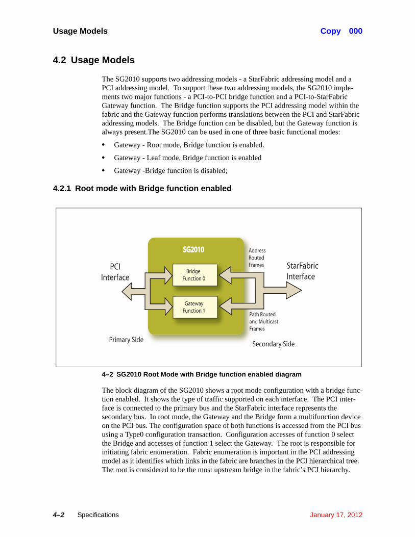
4.2.1 Root mode with Bridge function enabled
4–2 SG2010 Root Mode with Bridge function enabled diagram
The block diagram of the SG2010 shows a root mode configuration with a bridge func-tion enabled. It shows the type of traffic supported on each interface. The PCI inter-face is connected to the primary bus and the StarFabric interface represents the secondary bus. In root mode, the Gateway and the Bridge form a multifunction device on the PCI bus. The configuration space of both functions is accessed from the PCI bus using a Type0 configuration transaction. Configuration accesses of function 0 select the Bridge and accesses of function 1 select the Gateway. The root is responsible for initiating fabric enumeration. Fabric enumeration is important in the PCI addressing model as it identifies which links in the fabric are branches in the PCI hierarchical tree. The root is considered to be the most upstream bridge in the fabric’s PCI hierarchy.
BridgeFunction 0
GatewayFunction 1
SSGG22001100
PCIInterface
Primary SideSecondary Side
Path Routedand MulticastFrames
AddressRoutedFrames StarFabric
Interface

January 17, 2012 Specifications 4–3
Copy 000 Usage Models
4.2.2 Leaf Mode with Bridge Function enabled
4–3 SG2010 Leaf mode with Bridge function enabled diagram
When the SG2010 is a leaf and the bridge function is enabled, the PCI interface is con-nected to the secondary bus and one of the ports on the StarFabric interface is the pri-mary bus. The block diagram shows the SG2010 in leaf mode. The Gateway is logically represented as a separate PCI device located on the Bridge’s secondary PCI bus. By default, the Bridge is fully transparent. Every PCI device downstream of the bridge including the gateway is fully visible to the host and their resources are mapped into the global PCI memory map. The SG2010 can also be configured to hide devices from the host.
4.2.3 Gateway-only usage model
4–4 SG2010 Gateway with Bridge function disabled diagram
In Gateway-only usage model, the Gateway is visible for PCI configuration from the PCI bus only. Since the Bridge function is required to create a PCI hierarchy in the fabric, using the Gateway-only usage model at the root prevents a PCI address-routed hierarchy from being con-structed, and isolates the entire fabric from the root’s PCI bus. Using the Gateway function at a leaf isolates a PCI subsystem from the PCI host.
Gateway
SG2010
PCI
InterfaceFabric
Interface
Path Routed
and Multicast
Frames
Gateway
Bridge
PCIInterface
Secondary SidePrimary Side
Path Routedand MulticastFrames
AddressRoutedFrames
Star FabricInterface
SG2010

Usage Models Copy 000
4–4 Specifications January 17, 2012
The only way to forward PCI transactions in Gateway-with bridge disabled is to translate between PCI transactions and path-routed or multicast frames. If the SG2010 is in gateway-only usage model and receives an address-routed frame, it drops the frame, signals an Address Rout-ing Failure event, and if a response frame is required, returns a SoftwareThe Gateway translates PCI transactions into path-routed or multicast frames.
4.2.4 SG2010 Functional Modes
4–1 Functional Modes
Mode PCI Configuration Notes
Bridge EnabledRoot Mode(Multifunction)
PCI is primary bus; fabric is secondary bus.
Bridge and Gateway provide a multifunction configuration interface to the host.
Only one node in the system can be configured as root.
Initiates fabric enumeration
Bridge Enabled Leaf Mode(Secondary subordinate)
PCI in secondary bus; fabric is primary bus.
Bridge and Gateway provide a hierarchical configuration model to the host.
Gateway is a PCI device on the secondary bus of the Bridge.
Enhanced addressing modes can be enabled on the Bridge.
Gateway must be able to respond to address-routed frames from the fabric addressing BAR0 or BAR1 (CSRs)
Gateway BARs have three modes of visibility to the host:
² All BARs visible² Only BAR0 and 1
Visible² Gateway not visible
Gateway-only Provides no address-routing support into or out of the fabric. Provides private local addressing support.
All frames translated are path-routed/multicast frames.

January 17, 2012 Specifications 4–5
Copy 000 Package Diagram
4.3 Package Diagram
Vss VSS
Vss VSS
VSS VSS
VSS VSS
VSS VSS
VSS VSS
VSS VSS
VSS VSS
vSSA
B
C
D
E
F
G
H
J
K
L
M
N
P
R
T
U
V
W
Y
1 2 3 4 5 6 7 8 9 10 11 12 13 14 15 16 17 18 19 20
BGA signal pin
I/O power = 3.3V
Core power = 1.5V
Ground
CDR Power=1.5V
VSSA

Package Diagram Copy 000
4–6 Specifications January 17, 2012
4.3.1 Pinout Diagram
SG2010
(272 Pins)
SG2010
(272 Pins)
AD [63:0]
CBE_L [7:0]
PAR
PAR64
REQ64_L
FRAME_L
IRDY_L
IDSEL
DEVSEL_L
ACK64_L
TRDY_L
STOP_L
PERR_L
SERR_L
INTA_L
INTB_L
INTC_L
INTD_L
PME_L
CLK
RST_L
RSTO_L
M66EN
VIO
LSTAT
HS_LED
ENUM_L
L64EN_L
LRST_L
BDSEL_L
REQ_L [0]/AGNT_L
GNT_L [0]/AREQ_L
REQ_L [6:1]
GNT_L [6:1]
REQ_L [8:7]/GPIO [6,4]
GNT_L [8:7]/GPIO [7,5]
GPIO[3:0]
PR_AD[0]/SR_DO
PR_AD[1]
PR_AD[2]/SKIPINS
PR_AD[3]/LEDHM
PR_AD[4]/PFN[0]
PR_AD[5]/LOCKOUT
PR_AD[6]/ARBEN
PR_AD[7]/CFEN
PR_RD_L
PR_WR_L
PR_CS_L/PR_RDY
PR_ALE_L/SR_DI
PR_CLK/SR_CK
SR_CS_L
ROOT
BRIDGE_EN
VDDG
VSSG
TSTCLKG
PLLCKLGO
TX0P [3:0]
TX0N [3:0]
TX1P [3:0]
TX1N [3:0]
RX0P [3:0]
RX0N [3:0]
RX1P [3:0]
RX1N [3:0]
REFCLKL
CTAP0 [3:0]
CTAP1 [3:0]
RESLO
RESHI
REF14
REF10
VDDA
VSSA
TSTCLKL
BYPASSL
RESETTX
TSTSHFTLD
ECSEL
ETOGGLE
EXDNUP
TSTPHASE
LOOPBKEN
TESTMUX[9:8]
LED1_L[3:0]/TESTMUX [7:4]
TESTMUX[7:4]/LED1_L[3:0]
LED0_L[3:0]/TESTMUX[3:0]
TESTMUX[3:0]/LED0_L[3:0]
TESTMODE[3:0]
TCK
TDI
TDO
TMS
TRST_L
SCAN_ENA
PCI
Interface
CompactPCI
Hot Swap
Interface
Configuration
Interface
PCI Arbiter
and GPIO
ROM
Interface
PLL
Interface
Link
Interface
Link
Interface Test
Pins
Test
Interface
JTAG
Interface
LEDs
PLL_RESET
TESTRST

January 17, 2012 Specifications 4–7
Copy 000 Pin List
4.4 Pin List
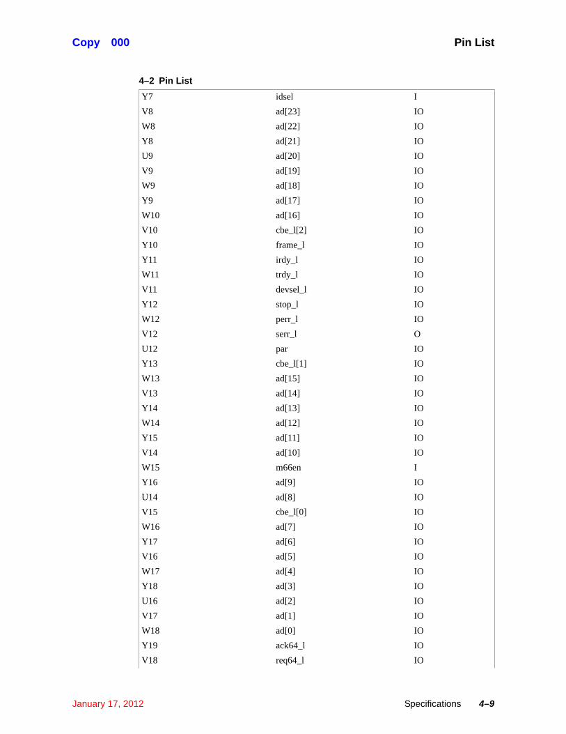
4–2 Pin List
Pin Signal Name Type
B1 tstshftld I
C2 ecsel I
D2 etoggle I
D3 exdnup I
E4 tstphase I
C1 testmux[9] IO
D1 testmux[8] IO
E3 led1_l[3]/testmux[7] IO
E2 led1_l[2]/testmux[6] IO
E1 led1_l[1]/testmux[5] IO
F3 led1_l[0]/testmux[4] IO
G4 led0_l[3]/testmux[3] IO
F2 led0_l[2]/testmux[2] IO
F1 led0_l[1]/testmux[1] IO
G3 led0_l[0]/testmux[0] IO
G2 reserved[4] IO
G1 PLL-Reset IO
H3 reserved[2] IO
H2 reserved[1] IO
H1 reserved[0] IO
J4 enum_l O
J3 hs_led O
J2 lstat I
J1 lrst_l I
K2 l64en_l I
K3 bdsel_l I
K1 root I
L1 bridge_en I
L2 rsto_l O
L3 scan_ena I
M1 gnt_l[0]/areq_l IO
M2 req_l[0]/agnt_l IO
M3 gnt_l[1] IO
M4 req_l[1] IO

Pin List Copy 000
4–8 Specifications January 17, 2012
N1 gnt_l[2] IO
N2 req_l[2] IO
N3 gnt_l[3] IO
P1 req_l[3] IO
P2 gnt_l[4] IO
R1 req_l[4] IO
P3 gnt_l[5] IO
R2 req_l[5] IO
T1 gnt_l[6] IO
P4 req_l[6] IO
R3 gnt_l[7]/gpio[5] IO
T2 req_l[7]/gpio[4] IO
U1 gnt_l[8]/gpio[7] IO
T3 req_l[8]/gpio[6] IO
U2 gpio[3] IO
V1 gpio[2] IO
T4 gpio[1] IO
U3 gpio[0] IO
V2 trst_l I
W1 tck I
V3 tms I
W2 tdo O
Y1 tdi I
W3 inta_l O
Y2 intb_l O
W4 intc_l O
V4 intd_l O
U5 rst_l I
Y3 clk I
Y4 pme_l O
V5 ad[31] IO
W5 ad[30] IO
Y5 ad[29] IO
V6 ad[28] IO
U7 ad[27] IO
W6 ad[26] IO
Y6 ad[25] IO
V7 ad[24] IO
W7 cbe_l[3] IO
4–2 Pin List
January 17, 2012 Specifications 4–9
Copy 000 Pin List
Y7 idsel I
V8 ad[23] IO
W8 ad[22] IO
Y8 ad[21] IO
U9 ad[20] IO
V9 ad[19] IO
W9 ad[18] IO
Y9 ad[17] IO
W10 ad[16] IO
V10 cbe_l[2] IO
Y10 frame_l IO
Y11 irdy_l IO
W11 trdy_l IO
V11 devsel_l IO
Y12 stop_l IO
W12 perr_l IO
V12 serr_l O
U12 par IO
Y13 cbe_l[1] IO
W13 ad[15] IO
V13 ad[14] IO
Y14 ad[13] IO
W14 ad[12] IO
Y15 ad[11] IO
V14 ad[10] IO
W15 m66en I
Y16 ad[9] IO
U14 ad[8] IO
V15 cbe_l[0] IO
W16 ad[7] IO
Y17 ad[6] IO
V16 ad[5] IO
W17 ad[4] IO
Y18 ad[3] IO
U16 ad[2] IO
V17 ad[1] IO
W18 ad[0] IO
Y19 ack64_l IO
V18 req64_l IO
4–2 Pin List

Pin List Copy 000
4–10 Specifications January 17, 2012
W19 cbe_l[7] IO
Y20 cbe_l[6] IO
W20 cbe_l[5] IO
V19 cbe_l[4] IO
U19 par64 IO
U18 ad[63] IO
T17 ad[62] IO
V20 ad[61] IO
U20 ad[60] IO
T18 ad[59] IO
T19 ad[58] IO
T20 ad[57] IO
R18 ad[56] IO
P17 ad[55] IO
R19 ad[54] IO
R20 ad[53] IO
P18 ad[52] IO
P19 ad[51] IO
P20 ad[50] IO
N18 ad[49] IO
N19 ad[48] IO
N20 ad[47] IO
M17 ad[46] IO
M18 ad[45] IO
M19 ad[44] IO
M20 ad[43] IO
L19 ad[42] IO
L18 ad[41] IO
L20 ad[40] IO
K20 ad[39] IO
K19 ad[38] IO
K18 ad[37] IO
J20 vio I
J19 ad[36] IO
J18 ad[35] IO
J17 ad[34] IO
H20 ad[33] IO
H19 ad[32] IO
H18 testmode[3] I
4–2 Pin List

January 17, 2012 Specifications 4–11
Copy 000 Pin List
G20 testmode[2] I
G19 testmode[1] I
F20 testmode[0] I
G18 pr_ad[7]/CFEN IO
F19 pr_ad[6]/ARBEN IO
E20 pr_ad[5]/LOCKOUT IO
G17 pr_ad[4]/PFN[0] IO
F18 pr_ad[3]/LEDHM IO
E19 pr_ad[2]/SKIPINS IO
D20 pr_ad[1] IO
E18 pr_ad[0]/SR_DO IO
D19 pr_rd_l O
C20 pr_wr_l O
E17 pr_cs_l IO
D18 pr_ale_l O
C19 pr_clk O
B20 sr_cs_l O
C18 tstclkg I
B19 pllclkgo O
A20 testrst I
A19 rx0p[0] I
B18 rx0n[0] I
B17 ctap0[0] I
C17 rx0p[1] I
D16 rx0n[1] I
A18 ctap0[1] I
A17 ctap0[2] I
C16 rx0p[2] I
B16 rx0n[2] I
A16 ctap0[3] I
C15 rx0p[3] I
D14 rx0n[3] I
B15 rx1p[0] I
A15 rx1n[0] I
C14 ctap1[0] I
B14 rx1p[1] I
A14 rx1n[1] I
C13 ctap1[1] I
B13 rx1p[2] I
4–2 Pin List

Pin List Copy 000
4–12 Specifications January 17, 2012
4.4.1 Power Pins
A13 rx1n[2] I
D12 ctap1[2] I
C12 rx1p[3] I
B12 rx1n[3] I
A12 ctap1[3] I
B11 tx0p[0] O
C11 tx0n[0] O
A11 tx0p[1] O
A10 tx0n[1] O
B10 tx0p[2] O
C10 tx0n[2] O
A9 tx0p[3] O
B9 tx0n[3] O
C9 reslo I
D9 reshi I
A8 ref14 I
B8 ref10 I
B7 tx1p[0] O
A6 tx1n[0] O
C7 tx1p[1] O
B6 tx1n[1] O
D7 tx1p[2] O
C6 tx1n[2] O
B5 tx1p[3] O
A4 tx1n[3] O
C4 tstclkl I
B3 refclkl I
B2 bypassl I
A2 resettx I
C3 loopbken I
4–3 Power Pins
Ground A1,D4,D8,D13,D17,H4,H17,J9,J10,J11,J12,K9,K10,K11,K12,L9,L10,L11,L12,M9,M10,M11,M12,N4,N17,U4,U8,U13,U17
Vdd 3.3V D10,D11,F4,F17,R4,R17,U10,U11
Vdd 1.5V D6, D15, K4, K17, L4 ,L17,U6,U15,A5
4–2 Pin List
January 17, 2012 Specifications 4–13
Copy 000 Pin Descriptions
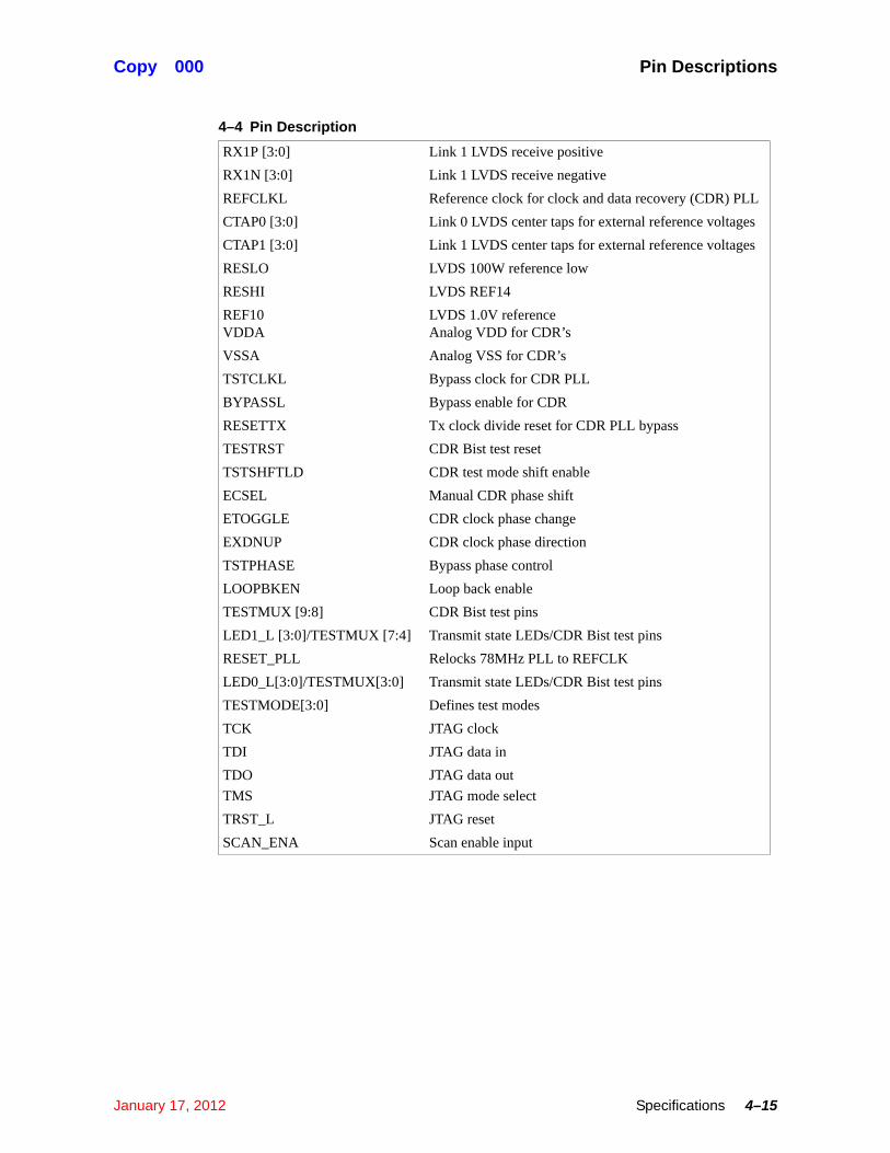
4.5 Pin Descriptions
CDR Vdda 1.5 C5,A3
CDR Vssa B4,D5
Global PLL Vddg 1.5 C8
Global PLL Vssg A7
4–4 Pin Description
AD [63:0] PCI multiplexed address/data bus.
CBE_L [7:0] PCI multiplexed command/byte enable bus
PAR PCI parity pin
PAR 64 PCI 64-bit extension parity pin.
REQ64_L PCI 64 bit transaction request
FRAME_L PCI transaction frame.
IRDY_L PCI initiator ready
IDSEL PCI configuration device select
DEVSEL_L PCI target device select
ACK64_L PCI 64 -bit transaction acknowledge
TRDY_L PCI target ready
STOP_L PCI target transaction termination
PERR_L PCI parity error detected
SERR_L PCI system error
INTA_L PCI device interrupt signal A
INTB_L PCI device interrupt signal B
INTC_L PCI device interrupt signal C
INTD_L PCI device interrupt signal D
PME_L PCI power managerment interrupt
CLK PCI clock input
RST_L PCI Platform reset input
M66EN PCI 66MHz enable
VIO PCI I/O voltage bias
LSTAT CompactPCI Hot Swap ejector handle switch status.
HS_LED CompactPCI Hot Swap LED Control
ENUM_L CompactPCI Hot Swap interrupt
L64EN_L CompactPCI Hot Swap local 64-bit extension enable
LRST_L CompactPCI Hot Swap local reset
BDSEL_L CompactPCI Hot Swap board seated
REQ_L[0]/AGNT_L PCI Arbiter input/SG2010 PCI GNT INPUT
4–3 Power Pins

Pin Descriptions Copy 000
4–14 Specifications January 17, 2012
GNT_L [0]/AREQ_L PCI arbiter output/SG2010 PCI REQ OUTPUT
REQ_L[6:1] PCI arbiter dedicated request inputs
GNT_L [6:1] PCI arbiter dedicated grant outputs
REQ_L[8:7]/GPIO[6,4] PCI Arbiter shared request inputs. PCI bus arbiter is used and these pins are enabled as arbiter pins, these pins are PCI request inputs for up to two PCI bus masters/General purpose I/O pins
GPIO [7,5]/ GNT_L[8:7] General purpose I/O pins/ PCI arbiter shared grant out-puts. PCI bus arbiter is used and these pins are enabled as arbiter pins, these pins are PCI request.
GPIO[3:0] General purpose I/O pins
PR_AD[0:7] Shared pins between the parallel ROM multiplexed address/data bus, serial ROM data output signal
SR_DO Serial ROM Data output signal
SKIPINS SKIPINS causes hot swap controller to skip an insertion interrupt on power-up
PR_RD_L Parallel ROM read strobe
PR_WR_L Parallel ROM write strobe
PR_CS_L Parallel ROM chip select output/device ready input. When the parallel ROM interface is not in multi-function mode.
PR_RDY When the parallel ROM interface is in multi-function mode, the SG2010 samples this signal as a device ready signal.
PR_ALE_L Parallel ROM address latch enable
SR_DI Serial ROM data input
PR_CLK Parallel ROM address latch clock
SR_CK Serial ROM clock
SR_CS_L Serial ROM chip select
ROOT When ROOT is high, the SG2010 is configured as a root
BRIDGE_EN When BRIDGE_EN is high, the SG2010 Bridge function is enabled
VDDG VDD for 78MHz Global PLL
VSSG VSS for 78MHz Global PLL
TSTCLKG Reference clock and bypass clock for 78MHz PLL
PLLCLKGO 78MHz PLL output
TX0P[3:0] Link 0 LVDS transmit positive
TX0N [3:0] Link 0 LVDS transmit negative
TX1P [3:0] Link 1 LVDS transmit positive
TX1N [3:0] Link 1 LVDS transmit negative
RX0P [3:0] Link 0 LVDS receive positive
RX0N [3:0] Link 0 LVDS receive negative
4–4 Pin Description
January 17, 2012 Specifications 4–15
Copy 000 Pin Descriptions
RX1P [3:0] Link 1 LVDS receive positive
RX1N [3:0] Link 1 LVDS receive negative
REFCLKL Reference clock for clock and data recovery (CDR) PLL
CTAP0 [3:0] Link 0 LVDS center taps for external reference voltages
CTAP1 [3:0] Link 1 LVDS center taps for external reference voltages
RESLO LVDS 100W reference low
RESHI LVDS REF14
REF10 LVDS 1.0V referenceVDDA Analog VDD for CDR’s
VSSA Analog VSS for CDR’s
TSTCLKL Bypass clock for CDR PLL
BYPASSL Bypass enable for CDR
RESETTX Tx clock divide reset for CDR PLL bypass
TESTRST CDR Bist test reset
TSTSHFTLD CDR test mode shift enable
ECSEL Manual CDR phase shift
ETOGGLE CDR clock phase change
EXDNUP CDR clock phase direction
TSTPHASE Bypass phase control
LOOPBKEN Loop back enable
TESTMUX [9:8] CDR Bist test pins
Transmit state LEDs/CDR Bist test pins
Relocks 78MHz PLL to REFCLK
Transmit state LEDs/CDR Bist test pins
LED1_L [3:0]/TESTMUX [7:4]
RESET_PLL
LED0_L[3:0]/TESTMUX[3:0]
TESTMODE[3:0] Defines test modes
TCK JTAG clock
TDI JTAG data in
TDO JTAG data out
TMS JTAG mode select
TRST_L JTAG reset
SCAN_ENA Scan enable input
4–4 Pin Description
Pin Descriptions Copy 000
4–16 Specifications January 17, 2012
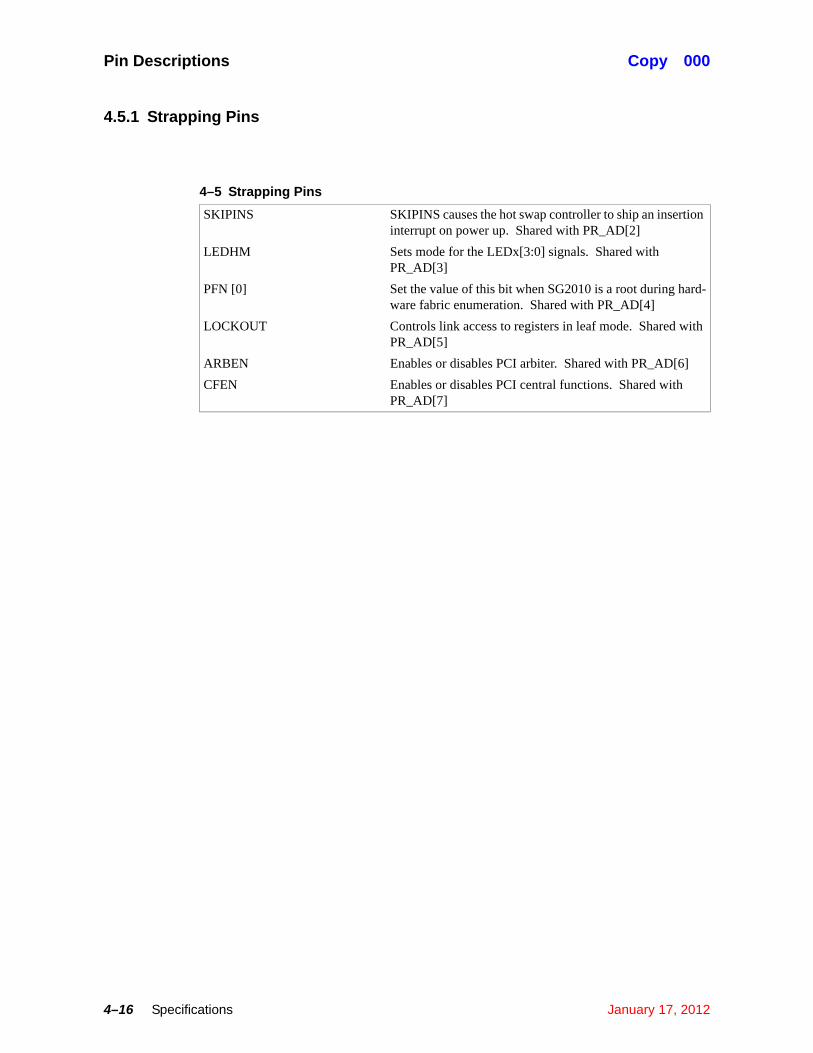
4.5.1 Strapping Pins
4–5 Strapping Pins
SKIPINS SKIPINS causes the hot swap controller to ship an insertion interrupt on power up. Shared with PR_AD[2]
LEDHM Sets mode for the LEDx[3:0] signals. Shared with PR_AD[3]
PFN [0] Set the value of this bit when SG2010 is a root during hard-ware fabric enumeration. Shared with PR_AD[4]
LOCKOUT Controls link access to registers in leaf mode. Shared with PR_AD[5]
ARBEN Enables or disables PCI arbiter. Shared with PR_AD[6]
CFEN Enables or disables PCI central functions. Shared with PR_AD[7]
January 17, 2012 Specifications 4–17
Copy 000 Package Specification
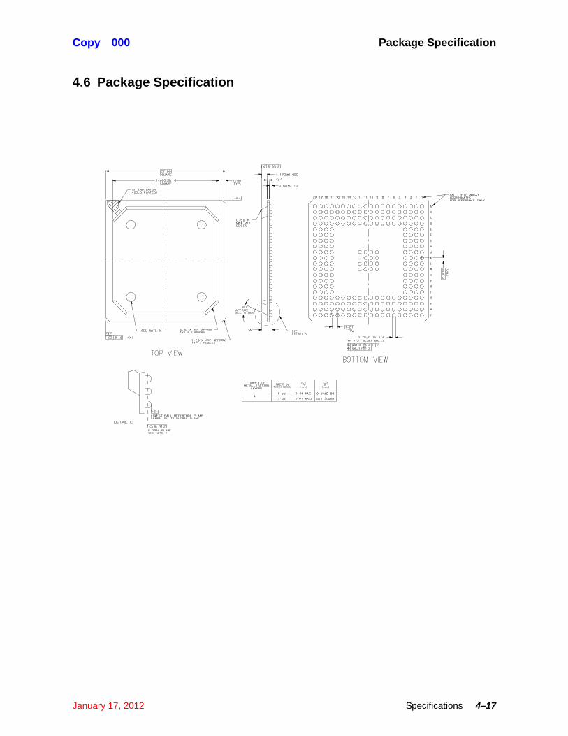
4.6 Package Specification

Package Specification Copy 000
4–18 Specifications January 17, 2012

January 17, 2012 Electrical Specifications 5–1
Copy 000
5
Electrical Specifications
5.1 Absolute Maximum Ratings
5.2 DC Specifications
Table 0–1 Absolute Maximum Ratings
Max Junction Temperature 125 degrees C
Core Supply Voltage 1.5V +/-5%
I/O Supply Voltage 3.3V +/-5%
Storage Temperature -55 to 125 degrees C
Operating Temperature -40 to Max Junction Temp 125 degrees C
Theta-Jb 14.2 C/W
Theta-Jc 7.9 C/W
Theta-Ja 22.8C /W
Theta-Jma at 1.0 m/s (~200ft/min): 18.4 C/W
Theta-Jma at 2.5 m/s (~500 ft/min) 16.7 C/W
Power dissipation 2.15W maximum
Table 0–2 DC Specifications (non-LVDS signals)
Symbol Parameter Condition Min Max
Vih Input high voltage – .5Vcc .5Vcc+.5V
Vil Input low voltage – -0.5V .3Vcc
Vipu Input Pull-up voltage – .7Vcc –
Voh Output high voltage Ioh = -500A .9Vcc –
Vol Output low voltage Iol = 1500A – .1Vcc
Iin Input leakage current 0 < Vin < Vio – + 10 A
Iin-pme PME_L input leakage Vo < 3.6VVcc off
– -1 mA
Cin Pin capacitance – – 10 pF

DC Specifications Copy 000
5–2 Electrical Specifications January 17, 2012
* Refer to appendix A for application note relating to industrial temperature operation.
Table 0–3 DC Supply Current
Symbol Conditions Max Current (mA)
Icore 1.5V +/- 5% 342
Iio 3.3V +/- 5% 479

January 17, 2012 Electrical Specifications 5–3
Copy 000 Timing Specifications
5.3 Timing Specifications
5.3.1 PCI Interface
The PCI interface AC specifications are compliant to the PCI Local Bus Specification, Revision 2.2
Table 0–4 PCI Signal AC Specifications
Signal Symbol Parameter Min Max
CLK Tcyc Cycle time 15ns 40ns
CLK Thigh Time high 6ns –
CLK Tlow Time low 6ns –
CLK Slew rate 1.5 V/ns 4 V/ns
Bused PCI outputs Tval CLK to valid 2ns 6ns
Point-to-point PCI outputs Tval(ptp) CLK to valid 2ns 6ns
All PCI outputs Ton Hi-Z to driven 2ns –
All PCI outputs Toff Driven to Hi-Z – 14ns
Bused PCI inputs Tsu Setup to CLK 3ns –
Point-to-point PCI Inputs Tsu(ptp) Setup to CLK 5ns –
All PCI inputs Th Hold from CLK 0ns –
RST_L Trst Active after power stable 1ms –
RST_L Trst-clk Active after clocks stable 100µs –
All PCI outputs, tri-stated Trst-off RST_L to Hi-Z – 40ns
REQ64_L Trrsu Setup to RST_L 10Tcyc ns –
REQ64_L Trrh Hold from RST_L 0ns 50ns
PR_AD[7:2] Tsrh Hold from RST_L 0ns 50ns
FRAME# for cfg access Trhfa From RST_L deasserted 225 clocks –
Any FRAME# assertion Trhff From RST_L deasserted 5 clocks –
INTx_L, ENUM_L, PME_L, SERR_L
Asynchronous

Timing Specifications Copy 000
5–4 Electrical Specifications January 17, 2012
5.3.2 Parallel and Serial ROM Interface
(1) Programmable by software
Table 0–5 Parallel and Serial ROM AC Specifications
Signal Symbol Parameter Min Max
PR_AD[7:0] Tadsu Setup to PR_RD_L rising 30ns –
PR_AD[7:0] Tadh Hold from PR_RD_L rising 30ns –
PR_AD[7:0] Tadval Valid from PR_CLK falling 0ns 8ns
PR_CS_L Tpcsl (1) Time low 480ns 15.36µs
PR_CS_L Tpcss (1) Setup to PR_RD_L or PR_WR_L falling Tprcyc –
PR_ALE_L Tasu Setup to PR_CLK rising .5*Tprcyc –
PR_ALE_L Tasucs Setup to PR_CS_L falling Tprcyc –
PR_CLK Tprcyc Cycle time 60ns 1.92µs
SR_CLK Tscyc Cycle time 510ns –
SR_CS_L Tscsl Minimum time low 56.5*Tscyc –
SR_CS_L Tscssu Setup to SR_CLK rising .5*Tscyc –
SR_DO Tsdosu Setup to SR_CLK rising 30ns –
SR_DO Tsdoh Hold from SR_CLK rising 30ns –
SR_DI Tsdivalb Valid before SR_CLK rising .5*Tscyc –
SR_DI Tsdivala Valid from SR_CLK rising .5*Tscyc –

January 17, 2012 Electrical Specifications 5–5
Copy 000 Timing Specifications
5.3.3 Reference ClockTiming
5.3.4 Global PLL Bypass Clock
5.3.5 StarFabric Interface Timing
The LVDS transmitters and receivers are compliant to the IEEE 1596.3 and EIA/TIA-644 LVDS specifications.
(2) Test conditions: ZL=100Ohm±1%, Cpad=3.0pF, Cpadn=3.0pF(3) UI = Unit Interval, which is 1.6075ns for 622.208 Mbit/s data(4) This should not occur more than once per minute
Table 0–6 Reference Clock AC Specifications
Signal Symbol Parameter Min Max
REFCLKL Fxtal Frequency 62.208MHz - 25ppm
62.208MHz + 25ppm
REFCLKL peak-to-peak jitter 100ps
REFCLKL Duty Cycle 40% 60%
REFCLKL 78MHz PLL Reset after 1.5VDD > 1.32V
3ms
Table 0–7 Global PLL Bypass Clock AC Specifications
Signal Symbol Parameter Min Max
TSTCLKG Fxtal Frequency 77.76MHz -100ppm
77.76MHz + 100ppm
TSTCLKG peak-to-peak jitter 150ps
TSTCLKG Duty Cycle 45% 55%
Table 0–8 StarFabric LVDS Interface AC timing
Signal Symbol Parameter Min Max
TXnP, TXnN Ttdpsk Differential skew – 50ps
TXnP, TXnN Ttdpr (2) Low to high time 100ps 210ps
TXnP, TXnN Ttdpf (2) High to low time 100ps 210ps
TXnP, TXnN Ttjtr (3) Output Jitter, Generated250 kHz to 5 MHz
– .18 UI p-p
RXnP, RXnN Trjtr (3) Jitter Tolerance250 kHz25 kHz2 kHz
–0.6 UI p-p6 UI p-p60 UI p-p
RXnP, RXnN Trppsk Pair to pair skew – 2ns
RXnP, RXnN Treye (3) Eye Opening 0.4 UI p-p
RXnP, RXnN Trsntb (4) Stream of non-transitional bits – 60 bits

Timing Specifications Copy 000
5–6 Electrical Specifications January 17, 2012
5.3.6 JTAG Timing
5.3.7 Asynchronous and Static Signals
Table 0–9 JTAG Signal AC TIming Specifications
Signal Symbol Parameter Min Max
TCK Fftck Frequency – 10MHz
TCK Ttckl Time low 50ns –
TCK Ttckh Time high 50ns –
TDI, TMS Ttsu Setup to TCK 40ns –
TDI, TMS Tth Hold from TCK 40ns –
TDO Ttval Valid from TCK – 30ns
TDO Ttz Hi-Z from TCK 5ns 40ns
Table 0–10 Asynchronous and Static Signals
Signal Note
GPIO[7:0] Under software control
INTx_L, PME_L, ENUM_L Interrupt inputs/outputs. Assume asynchronous to PCI CLK
LSTAT, L64EN_L, BDSEL_L Hot swap signals. Static or asynchronous
M66EN 66Mhz Enable. Static.
ROOT, BRIDGE_EN Static
CTAP0[3:0], CTAP1[3:0], RESLO, RESHI
LVDS control. Static.
BYPASSL, RESETTX, RESETRX, TSTSHFTLD, ECSEL, ETOGGLE, EXDNUP, TSTPHASE, LOOPBKEN
Asynchronous
TESTMODE[3:0] Static

January 17, 2012 Electrical Specifications 5–7
Copy 000 Timing Specifications
0.1 Internal Pull-up and Pull-down Resistors
Table 5–1 describes the internal pull-down and pull-up resistors on the SG2010. All internal pull-down and pull-up resistors are 50 k . At the board level, these pins can either be left unconnected or connected through a smaller resistor to override the inter-nal value, if needed for test or diagnostic purposes.
5–1 Internal Pull-up and Pull-down Resistors
Signal Name Internal pull-up/pull-down Functional Value
BYPASSL 0 0
ECSEL 0 0
ETOGGLE 0 0
EXDNUP 0 0
PLL_RESET 0 0
LOOPBKEN 0 0
RESETTX 0 0
SCAN_ENA 0 0
TESTRST 0 0
TSTCLKG 0 0
TSTCLKL 0 0
TSTPHASE 0 0
TSTSHFTLD 0 0
TCK 1 1
TDI 1 1
TMS 1 1
TRST_L 1 0

Timing Specifications Copy 000
5–8 Electrical Specifications January 17, 2012

January 17, 2012 Industrial Temperature 6–1
Copy 000
6
Industrial Temperature
6.1 Abstract
To ensure that the SG2010 PCI to StarFabric bridge operates properly in industrial tem-perature range applications, the use of an external 77.76 MHz clock source is required. The external clock source provides the SG2010 with appropriate clocking at tempera-tures ranging from -40ºC to +85ºC. The existing internal PLL supports a temperature range from 0ºC to 70ºC. This application note outlines the modifications required to implement the external clock source.
6.2 Clock Details
The SG2010 bridge has two distinct types of PLLs, one associated with the clock-data recovery (CDR) in the SERDES, and a global PLL that generates a clock for internal logic. Both the CDR and global PLLs use the 62.208 MHz reference input clock.
The global PLL implements a multiply/divide clock multiplication function. The result-ing internal global clock is roughly 78 MHz in the SG2010. This PLL goes through an auto-trimming process to optimize its performance. The synthesized 78 MHz clock is appropriate for all applications rated for a temperature range from 0ºC to 70ºC.
However when using the SG2010 in an environment outside of the commercial 0ºC to +70ºC specification, the global PLL is not guaranteed to function properly. An external clock source is required for these applications. Note that the 62.208 MHz reference clock is still required for the CDR when the global PLL is being bypassed.
6.3 Design Guidelines
When using the SG2010 above the 70 degree C commercial specification, the internal global PLL needs to be bypassed and an external 77.76 MHz clock source is to be used. The hardware implementation is shown in Figure 0–1 and described below:
1. Set the SG2010 into PLL bypass mode by setting the TESTMODE<3:0> inputs to a <0001>, thereby forcing the SG2010 to use an external 77.76 MHz oscillator instead of the internally generated clock. The TESTMODE<3:0> signals are located at BGA ball positions H18, G20, G19, and F20 respectively. TEST-MODE<3:1> can be signaled low with pull-down resistors and TESTMODE<0> can be signaled high with a pull-up resistor.

Design Guidelines Copy 000
6–2 Industrial Temperature January 17, 2012
2. Connect a 77.76 MHz clock oscillator to the TSTCLKG signal pin (BGA ball C18) of the device. Include an appropriate value series damping resistor between the clock oscillator’s output and the SG2010’s TSTCLKG input. This resistor should be placed close to the source of the clock.
Figure 0–1 Recommended Modification
Oscillator Specifications
Frequency: 77.76 MHz 100ppm
Jitter: 150ps peak-to-peak max
Duty Cycle: 45/55% min/max
Voltage Supply: 3.3 Volts DC
Operating Temperature:-40°C to 85°C
77.76 MhzOSC
0.01uF
3.3V
SG2010
TSTCLKG (C18)
TESTMODE0 (F20)
TESTMODE1 (G19)
TESTMODE2 (G20)
TESTMODE3 (H18)
10K
3.3V
10K 10K10K
43 OUTVCC
GND

January 17, 2012 Contact Information 7–1
Copy 000
7
Contact Information
7.1 Ordering Information
7.2 Headquarters
Dolphin Inc.
7 Boomhower Rd.
Woodsville, NH 03785
Voice: (603) 747-4100
Fax: (603) 747-4101
Web: www.dolphinics.com
Email: Info@ dolphinics.com
7–1 Part Numbers
Part Number Description
SG2010-A4 PCI to StarFabric Bridge
L-SG2010-A4 PCI to StarFabric Bridge Lead Free Package