pcb design guideline and thermal analysis for gan ... systems_gn005 app... ·...
TRANSCRIPT

APPLICATION NOTE
GN005 Rev 2014-11-04 © 2009 - 2014 GaN Systems Inc. 1
Thermal Analysis and PCB Design Guidelines for GaN Enhancement Mode Power Switching Transistors
This application note sets out thermal design guidelines and PCB layout considerations for GaN Systems enhancement mode power switching transistors. It introduces the advanced features of the GaNPX™ package and it provides a comparative analysis of various different PCB thermal design choices.
1. Device Thermal characteristics The GaNP package, shown in Figure 1, is the first implementation of a discrete GaN power device to be embedded within a laminate construction. A series of galvanic processes [1] replace conventional packaging techniques such as clips, wire bonds and molding compounds. The GaN die is protected within the laminate construction. Figure 1 provides a cross sectional view, showing how a series of printed circuit board plating steps form source and drain bus bars that significantly augment the current carrying capacity of the conventional die metallization. This greatly reduces the critical loop inductance and hence the difficulties of driving the high speed, high current switch. When carefully implemented, the new embedded power GaN devices provide a small volume, low resistance and low inductance package.
The embedding technique has been implemented in three package sizes. provides the package size, die and pad size. GS66508P was selected for this thermal analysis.
Part Number Package Size (mm)
Package Area (mm2)
Die Pad Size (mm)
Die Pad Area (mm2)
GS66504P 6.4/8.63/0.45 55.23 2.13/3.9 8.31
GS66506P 7.9/8.63/0.45 68.18 2.13/5.4 11.48
GS66508P 9.2/8.63/0.45 79.4 2.13/6.7 14.27
Table 1: GaNPX package geometrical characteristics
Figure 1: GaNPX package cross section view
APPLICATION NOTE
GN005 Rev 2014-11-04 © 2009 - 2014 GaN Systems Inc. 2
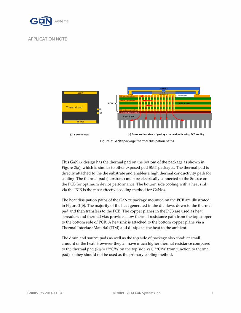
Figure 2: GaNPX package thermal dissipation paths
This GaNPX design has the thermal pad on the bottom of the package as shown in Figure 2(a), which is similar to other exposed pad SMT packages. The thermal pad is directly attached to the die substrate and enables a high thermal conductivity path for cooling. The thermal pad (substrate) must be electrically connected to the Source on the PCB for optimum device performance. The bottom side cooling with a heat sink via the PCB is the most effective cooling method for GaNPX.
The heat dissipation paths of the GaNPX package mounted on the PCB are illustrated in Figure 2(b). The majority of the heat generated in the die flows down to the thermal pad and then transfers to the PCB. The copper planes in the PCB are used as heat spreaders and thermal vias provide a low thermal resistance path from the top copper to the bottom side of PCB. A heatsink is attached to the bottom copper plane via a Thermal Interface Material (TIM) and dissipates the heat to the ambient.
The drain and source pads as well as the top side of package also conduct small amount of the heat. However they all have much higher thermal resistance compared to the thermal pad (RθJC =15°C/W on the top side vs 0.5°C/W from junction to thermal pad) so they should not be used as the primary cooling method.
Thermal pad
Drain
Source
G
SS
(a) Bottom view
GaNPx
DieSource Thermal Pad Drain
PCB top copper layer
PCB bottom copper layerThermal interface material
Heat Sink
PCB
Thermal vias
(b) Cross section view of package thermal path using PCB cooling
FR4 CoreInternal copper layer

APPLICATION NOTE
GN005 Rev 2014-11-04 © 2009 - 2014 GaN Systems Inc. 3
2. PCB design considerations Appropriate PCB design is essential for the thermal management of GaNPX package and the PCB thermal resistance is the primary consideration for overall system thermal performance. There are several key factors that impact the PCB thermal performance:
Heat spreading copper pad The top copper pad plays the important role of conducting the heat from the small area under the device to a larger area on the PCB. As such, the top copper layer must have sufficient thickness to provide enough heat spreading. The internal and bottom layers also improve heat spreading if thermal vias are used. The bottom copper pad serves as the contact surface to the heatsink or Thermal Interface Material (TIM) and it should have sufficient coverage to allow optimum heat transfer to the heatsink.
Thermal vias The most effective way to improve vertical heat transfer for an FR-‐‑4 PCB is to add plated through-‐‑hole thermal vias between conductive layers. Since FR-‐‑4 material has very low thermal conductivity, thermal via design is one of the dominating factors for total PCB thermal resistance.
Below are some considerations for the design of thermal vias:
• Adding open plated through vias to the SMT pad (“Via In Pad”) is not commonly done because it may create a solder-‐‑wicking issue: the solder tends to be wicked down into the vias during the reflow process and generates solder voids on the pad. The following steps can be taken to limit this problem:
o Use small via diameter. The surface tension of solder limits the amount of solder wicking on smaller vias. With 0.3mm or smaller via diameter, the solder wicking can be reduced.
o Fill the vias with thermally conductive materials. It eliminates the solder wicking but adds cost and an extra manufacturing step.
• 8mil (0.2mm) is the typical minimum mechanical drilling size. 12mil (0.3mm) is more common and lower cost.
• IPC-‐‑6012 specifies a minimum 20µμm (0.8mil) copper plating thickness for a Class 2 PCB. The standard via plating thickness is 25µμm (1mil), which will be used for this analysis.
• PCB thickness has an impact on the thermal via performance. The thermal resistance decreases if a thinner PCB is used.

APPLICATION NOTE
GN005 Rev 2014-11-04 © 2009 - 2014 GaN Systems Inc. 4
3. PCB Thermal Analysis Figure 3 shows a simplified thermal model for the GaNPX package mounted on a PCB, where RθJC = junction-‐‑to-‐‑case thermal resistance (package thermal resistance); RθPCB = PCB thermal resistance; RθTIM = thermal interface material (TIM) thermal resistance, and RθHSA = heat sink to ambient thermal resistance. The PCB thermal resistance RθPCB is of interest for this thermal analysis.
ElectroFlo® thermal analysis software was used for the simulation. All thermal simulations were conducted at a power dissipation of 10 W. An assumption was made that the surface temperature of the heatsink was constant and equal to 25 °C. GAP3000S30R (0.01” thickness) from Bergquist™[2] has a thermal conductivity of 3W/m·∙K and was selected for this thermal analysis.
PCB Setup This thermal analysis was based on following PCB setup:
• Single GS66508P 650V enhancement mode HEMT
• Device is placed at a 30mm by 30mm square PCB with thermal pad center located at the center of PCB.
• Standard 1.6mm (0.063”) FR-‐‑4 PCB (2 to 8 layers)
• 1oz or 2oz copper thickness for all layers
• Assume all copper layers are evenly distributed
Thermal vias:
• 12mil (0.3mm) diameter placed on 25mil (0.64mm) grid spacing • Standard 1mil (25µμm) copper plating thickness • No via filling
30.00
30.00
Thermal Pad
Figure 4: PCB Thermal analysis setup
GaNPxDie
Thermal Pad
Junction
Ambient
RθJC
PCB
TIM
Heat Sink
RθPCB
RθTIM
RθHSA
Figure 3: Junction-ambient thermal model

APPLICATION NOTE
GN005 Rev 2014-11-04 © 2009 - 2014 GaN Systems Inc. 5
PCB layout: copper area analysis To examine the impact of the copper area, 3 different PCB layouts were chosen for the thermal analysis:
PCB Layout #1:
Square copper pads (7mm by 7mm) are added on all internal and bottom layers, which is the minimum size to cover the thermal pad. Copper on the top layer connects the thermal pad to the source and its outline is limited by the clearance between the drain and source as well as the G/SS pads. 12mil (0.3mm) diameter vias are placed on a 25mil (0.64mm) grid and vias are only placed within a 7x7mm area, and kept out 2.7mm from the drain pad.
Figure 5: PCB Layout #1 (7mm x 7mm)
PCB Layout #2:
For this analysis the copper area is increased to 15mm by 15mm with a total of 284 vias with the same pattern as PCB#1. The top copper area is increased by about 2 times.
Figure 6: PCB Layout #2 (15mm x 15mm)
6.00
10.00
7.00
7.00
Gate Driver
2.70
Thermal Vias Pattern
Ø0.3mm (12mil)
0.64(25mil)
0.64
(25m
il)
Top Layer Internal/Bottom Layer(s)
(77 vias)
15.00
Gate Driver
15.0015.00
15.00
(284 vias)
Top Layer Internal/Bottom Layer(s)

APPLICATION NOTE
GN005 Rev 2014-11-04 © 2009 - 2014 GaN Systems Inc. 6
PCB Layout #3:
This layout has largest copper area (30mm x 30mm). The top copper layer only extends to the right and bottom as the left side of the device is reserved for the gate driver circuit and the top is limited by the clearance.
Figure 7: PCB Layout #2 (30mm x 30mm)
The table below summarizes and compares the copper areas of all 3 PCB layouts.
Top Cu layer (mm)
Approx. area (mm 2)
Internal & bottom Cu (mm)
Area (mm 2)
Total vias
PCB #1 10x6 60 7x7 49 77
PCB #2 15x8.6 129 15x15 225 284
PCB #3 22.5x8.6 193 30x30 900 680
Table 2: Copper area comparison of 3 PCB layouts
30.00
Gate Driver
30.0030.00
(860 vias)
22.50
16.50
Top Layer Internal/Bottom Layer(s)

APPLICATION NOTE
GN005 Rev 2014-11-04 © 2009 - 2014 GaN Systems Inc. 7
Three PCB layouts with different copper layer and thickness were analyzed. Figure 8 shows one example of thermal analysis results. The PCB thermal resistance RθPCB is defined by:
𝑹𝜽𝑷𝑪𝑩 =𝑻𝑻𝑶𝑷𝑴𝑨𝑿!𝑻𝑩𝑶𝑻𝑴𝑨𝑿
𝟏𝟎𝑾 (Eq.3)
Where TTOPMAX and TBOTMAX are the maximum temperatures on the top and bottom copper layers, which are located approximately at the center of the die.
Figure 8: Example of thermal simulation results (PCB#2 15mm x 15mm, 2oz copper, 4-layer)
Table 3: PCB thermal resistance RθPCB (°C/W)
# Cu Layers
PCB#1 1 oz
PCB#2 1 oz
PCB#3 1 oz
PCB#1 2 oz
PCB#2 2 oz
PCB#3 2 oz
2 6.38 5.45 5.44 6.00 4.68 4.65
4 6.17 4.95 4.86 5.69 4.17 4.04
6 5.98 4.58 4.44 5.38 3.8 3.61
8 5.8 4.27 4.07 5.07 3.45 3.22

APPLICATION NOTE
GN005 Rev 2014-11-04 © 2009 - 2014 GaN Systems Inc. 8
Figure 9: PCB thermal resistance for 3 PCB layouts (standard 1.6mm PCB and 0.3mm vias) The thermal analysis results are shown in Figure 9 and PCB#1 has the highest thermal resistance as expected. However PCB#3 provides very limited improvement on the thermal resistance compared to PCB#2 despite having a copper area 4 times bigger. With 2-‐‑4 layers, the thermal resistance of PCB#3 is almost same as PCB#2 and only 7% better with 8 layers and 2oz copper. This is due to the limited heat spreading on the top copper layer, as can be seen on the top view with vias in Figure 8. The copper and thermal vias become less effective when they are located further away from the heat source.
For all PCB layouts the thermal resistance decreases proportionally to the number of PCB layers. For PCB#3 with 2oz copper a 30% improvement on thermal resistance can be achieved by using an 8-‐‑Layer PCB, compared to a 2-‐‑layer design. Copper thickness is critical for horizontal heat conduction and thicker copper improves the heat spreading. 2oz copper provides about 20-‐‑25% improvement on the thermal resistance compared to 1oz copper.
Generally PCB#2 is the optimum layout among the 3 analysis cases. 2oz copper is recommended and, if the design allows, 4 or more PCB layers are recommended. For example a 2oz copper 6 layer PCB with copper features similar to PCB#2 will have a PCB thermal resistance close to 4˚C/W or about 5˚C/W for total junction to heatsink thermal resistance including the package and TIM.
APPLICATION NOTE
GN005 Rev 2014-11-04 © 2009 - 2014 GaN Systems Inc. 9
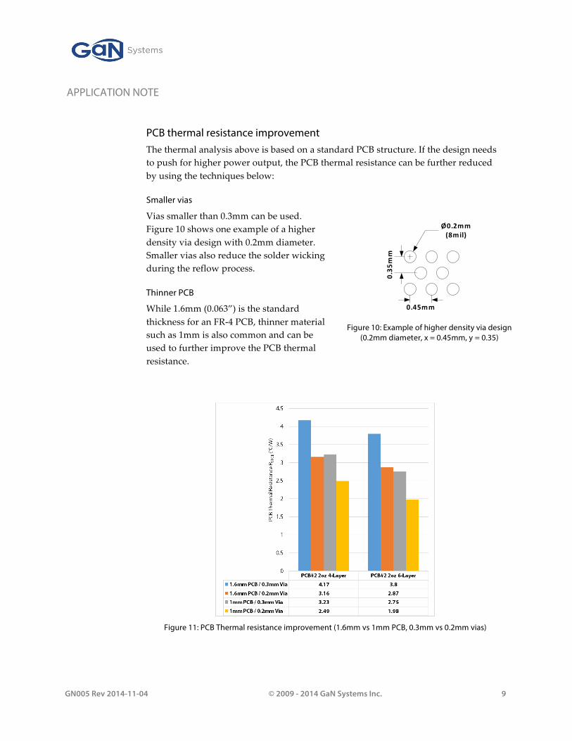
PCB thermal resistance improvement The thermal analysis above is based on a standard PCB structure. If the design needs to push for higher power output, the PCB thermal resistance can be further reduced by using the techniques below:
Smaller vias
Vias smaller than 0.3mm can be used. Figure 10 shows one example of a higher density via design with 0.2mm diameter. Smaller vias also reduce the solder wicking during the reflow process.
Thinner PCB
While 1.6mm (0.063”) is the standard thickness for an FR-‐‑4 PCB, thinner material such as 1mm is also common and can be used to further improve the PCB thermal resistance.
Figure 11: PCB Thermal resistance improvement (1.6mm vs 1mm PCB, 0.3mm vs 0.2mm vias)
0.45mm
0.35
mm
Ø0.2mm (8mil)
Figure 10: Example of higher density via design (0.2mm diameter, x = 0.45mm, y = 0.35)

APPLICATION NOTE
GN005 Rev 2014-11-04 © 2009 - 2014 GaN Systems Inc. 10
Figure 11 shows the thermal resistance results with different PCB thicknesses and via designs. A 25% reduction of PCB thermal resistance can be achieved by using 0.2mm via design. 1mm PCB thickness also improves the thermal resistance by 30%. By combining the smaller vias with a 1mm PCB, a thermal resistance of 2°C/W can be achieved on a 6-‐‑layer PCB with 2oz copper. However, not all PCB manufacturers are capable of producing reliable 1mm 6-‐‑layer PCB with 2oz copper. It is recommended to always confirm with your PCB manufacturer before using any PCB design discussed in this application note.
4. Maximum power capability Junction-to-Ambient Thermal Resistance The total junction to ambient thermal resistance RθJA of the power device is essential information for the designer to estimate the maximum power capacity of the system. It can be calculated using following equation:
RθJA = RθJC + RθPCB + RθTIM + RθHSA (Eq.4)
where RθPCB has been discussed in previous sections and RθJC is a fixed value that can be obtained from the device datasheet (0.5˚C/W for GS66508P). The heatsink to ambient RθHSA is largely dependent on the heatsink design and airflow.
Estimation of RθTIM The thermal resistance across the TIM, RθTIM, can be estimated using the following equation:
𝑹𝜽𝑻𝑰𝑴 = 𝑳/(𝑨 ∙𝑲) (Eq.5)
where L is the TIM thickness in m; A is the effective contact area (m2) and K is the thermal conductivity of the TIM in W/m·∙K, which can be obtained from the TIM datasheet. Note that A in the Eq.5 is not necessarily the total contact copper area at the bottom layer. Instead it is defined as the “effective” contact area depending on the PCB heat spreading. The effective contact area increases when thicker or more layers of copper are used. Figure 12 illustrates the thermal resistance breakdown for PCB#2 and shows that RθTIM ranges from less than 1 to 2˚C/W depending on the copper thickness and number of layers.

APPLICATION NOTE
GN005 Rev 2014-11-04 © 2009 - 2014 GaN Systems Inc. 11
Figure 12: Thermal Resistance Breakdown (PCB #2 15mm x 15mm) showing the variation of RθTIM
caused by the changing effective contact area
For a rule of thumb approximation, A = 50mm2 (about 4x the thermal pad area for the GS66508P, with a standard PCB structure using Cu pads and thermal vias) can be used to provide a reasonable estimation in the absense of detailed thermal simulation results.
The total junction to heatsink thermal resistances including the packaging and TIM for each PCB design are listed in Appendix A.1.
Power calculation Once the junction to ambient thermal resistance is determined, the maximum power dissipation allowed can be calculated using:
𝑷𝑫𝑴𝑨𝑿 = 𝜟𝑻𝑴𝑨𝑿/𝑹𝜽𝑱𝑨 (Eq.6)
where ΔTMAX is the maximum allowed temperature rising above ambient. Figure 14 shows the calculated maximum power dissipation vs heatsink-‐‑ambient thermal resistance (PCB#2, 4-‐‑6 layers and ΔTMAX = 50°C), which can be used to quickly evaluate system thermal performance. For example, a system design with heatsink-‐‑ambient thermal resistance of about 5°C/W and ΔTMAX = 50°C, would give a maximum allowed power loss of 5W per single device, using a 6-‐‑layer PCB#2 with 2oz copper and 0.3mm vias.
Figure 13: Approximate effective contact area for TIM (red dashed
line) for PCB#2

APPLICATION NOTE
GN005 Rev 2014-11-04 © 2009 - 2014 GaN Systems Inc. 12
Figure 14: Maximum power dissipation, GS66508P (PCB#2 15x15mm, 4-6 layers, 2oz Cu, ΔTMAX = 50°C)

APPLICATION NOTE
GN005 Rev 2014-11-04 © 2009 - 2014 GaN Systems Inc. 13
Appendix A.1 Thermal analysis results
* - Junction to heatsink RθJHS = RθJC + RθPCB + RθTIM
** - Maximum 6-Layer for 1mm PCB with 2oz copper
Table 4: Summary of thermal simulation results (°C/W) A.2 Impact of the number of thermal vias So far the maximum number of vias have been used for all the thermal analysis. As discussed before, the effectiveness of thermal vias degrades with increasing distance from the thermal pad. To further investigate this, the PCB thermal resistances were simulated with different numbers of vias. The PCB#2 with 2oz copper and 4 to 6 layers were selected for this analysis. Figure 15 depicts the relationship between the simulated thermal resistance and the number of vias. It can be seen that after a certain point, adding additional vias becomes a matter of diminishing returns. For example, a 15x8 (120) via matrix covering 49mm2 achieves 90% of the total thermal reduction obtained by 284 vias.
Therefore if the total number of vias must be reduced due to layout or cost constraints, it is recommended to cover at a minimum the 50mm2 area under the thermal pad with vias for optimum thermal performance.
RθPCB RθJHS* RθPCB RθJHS RθPCB RθJHS RθPCB RθJHS
1oz 1.6mm 6.38 9.44 6.17 8.93 5.98 8.64 5.8 8.42
1.6mm 6 8.45 5.69 7.99 5.38 7.65 5.07 7.34
1.0mm** 4.17 6.82 3.88 6.33 3.57 5.96
1oz 1.6mm 5.45 7.99 4.95 6.85 4.58 6.22 4.27 5.76
1.6mm 4.68 6.54 4.17 5.59 3.8 5.06 3.45 4.64
1.0mm 3.5 5.54 3.08 4.64 2.75 4.12
1.6mm 3.16 4.91 2.87 4.47
1.0mm 2.49 4.07 1.98 3.57
1oz 1.6mm 5.44 7.98 4.86 6.70 4.44 5.97 4.07 5.42
2oz 1.6mm 4.65 6.49 4.04 5.36 3.61 4.73 3.22 4.24
6-‐Layer 8-‐LayerPCB Layout Copper
PCB thickness Via Size
0.2mm
2-‐Layer 4-‐Layer
0.3mm
0.3mm
2ozPCB#1
PCB#2
PCB#3
2oz

APPLICATION NOTE
GN005 Rev 2014-11-04 © 2009 - 2014 GaN Systems Inc. 14
Figure 15: Diminishing return for thermal vias Summary This note has outlined PCB thermal design and layout considerations for using GaNPX devices in real applications. References
1) J. Roberts, T. MacElwee, and L. Yushyna, "ʺThe Thermal Integrity of Integrated GaN Power Modules"ʺ, IMAPS Conference & Exhibition on High Temperature Electronics Network (HiTEN 2013), pp.61-‐‑68, July 8-‐‑10, 2013, Oxford, UK.
2) http://www.bergquistcompany.com/thermal_materials/gap-‐‑pad.htm
www.gansystems.com North America � Europe � Asia
Important Notice – Unless expressly approved in writing by an authorized representative of GaN Systems, GaN Systems components are not designed, authorized or warranted for use in lifesaving, life sustaining, military, aircraft, or space applications, nor in products or systems where failure or malfunction may result in personal injury, death, or property or environmental damage. The information given in this document shall not in any event be regarded as a guarantee of performance. GaN Systems hereby disclaims any or all warranties and liabilities of any kind, including but not limited to warranties of non-infringement of intellectual property rights. All other brand and product names are trademarks or registered trademarks of their respective owners. Information provided herein is intended as a guide only and is subject to change without notice. The information contained herein or any use of such information does not grant, explicitly, or implicitly, to any party any patent rights, licenses, or any other intellectual property rights. GaN Systems standard terms and conditions apply. © 2009-2014 GaN Systems Inc. All rights reserved.