pca9535 pca9535c 16-bit i2c-bus and smbus, low …esd protection exceeds 2000 v hbm per jesd22-a114,...
TRANSCRIPT
1. General description
The PCA9535 and PCA9535C are 24-pin CMOS devices that provide 16 bits of General Purpose parallel Input/Output (GPIO) expansion for I2C-bus/SMBus applications and was developed to enhance the NXP Semiconductors family of I2C-bus I/O expanders. The improvements include higher drive capability, 5 V I/O tolerance, lower supply current, individual I/O configuration, and smaller packaging. I/O expanders provide a simple solution when additional I/O is needed for ACPI power switches, sensors, push buttons, LEDs, fans, etc.
The PCA9535 and PCA9535C consist of two 8-bit Configuration (Input or Output selection), Input, Output and Polarity Inversion (active HIGH or active LOW operation) registers. The system master can enable the I/Os as either inputs or outputs by writing to the I/O configuration bits. The data for each input or output is kept in the corresponding Input or Output register. The polarity of the read register can be inverted with the Polarity Inversion register. All registers can be read by the system master. Although pin-to-pin and I2C-bus address compatible with the PCF8575, software changes are required due to the enhancements and are discussed in Application Note AN469.
The PCA9535 is identical to the PCA9555 except for the removal of the internal I/O pull-up resistor which greatly reduces power consumption when the I/Os are held LOW.
The PCA9535C is identical to the PCA9535 except that all the I/O pins are high-impedance open-drain outputs.
The PCA9535 and PCA9535C open-drain interrupt output is activated when any input state differs from its corresponding Input Port register state and is used to indicate to the system master that an input state has changed. The power-on reset sets the registers to their default values and initializes the device state machine.
Three hardware pins (A0, A1, A2) vary the fixed I2C-bus address and allow up to eight devices to share the same I2C-bus/SMBus. The fixed I2C-bus address of the PCA9535 and PCA9535C are the same as the PCA9555 allowing up to eight of these devices in any combination to share the same I2C-bus/SMBus.
2. Features and benefits
Operating power supply voltage range of 2.3 V to 5.5 V
5 V tolerant I/Os
Polarity Inversion register
Active LOW interrupt output
Low standby current
Noise filter on SCL/SDA inputs
PCA9535; PCA9535C16-bit I2C-bus and SMBus, low power I/O port with interruptRev. 6 — 7 November 2017 Product data sheet

NXP Semiconductors PCA9535; PCA9535C16-bit I2C-bus and SMBus, low power I/O port with interrupt
No glitch on power-up
Internal power-on reset
16 I/O pins which default to 16 inputs
0 Hz to 400 kHz clock frequency
ESD protection exceeds 2000 V HBM per JESD22-A114, 200 V MM per JESD22-A115, and 1000 V CDM per JESD22-C101
Latch-up testing is done to JEDEC Standard JESD78 which exceeds 100 mA
Offered in four different packages: SO24, TSSOP24, HVQFN24 and HWQFN24
3. Ordering information
3.1 Ordering options
Table 1. Ordering information
Type number Topside marking
Package
Name Description Version
PCA9535D PCA9535D SO24 plastic small outline package; 24 leads; body width 7.5 mm SOT137-1
PCA9535PW PCA9535PW TSSOP24 plastic thin shrink small outline package; 24 leads; body width 4.4 mm
SOT355-1
PCA9535BS 9535 HVQFN24 plastic thermal enhanced very thin quad flat package; no leads; 24 terminals; body 4 4 0.85 mm
SOT616-1
PCA9535HF P35H HWQFN24 plastic thermal enhanced very very thin quad flat package; no leads; 24 terminals; body 4 4 0.75 mm
SOT994-1
PCA9535CD PCA9535CD SO24 plastic small outline package; 24 leads; body width 7.5 mm SOT137-1
PCA9535CPW PCA9535C TSSOP24 plastic thin shrink small outline package; 24 leads; body width 4.4 mm
SOT355-1
PCA9535CHF P35C HWQFN24 plastic thermal enhanced very very thin quad flat package; no leads; 24 terminals; body 4 4 0.75 mm
SOT994-1
Table 2. Ordering options
Type number Orderable part number
Package Packing method Minimum order quantity
Temperature
PCA9535D PCA9535D,112 SO24 STANDARD MARKING * IC'S TUBE - DSC BULK PACK
1200 Tamb = 40 C to +85 C
PCA9535D,118 SO24 REEL 13" Q1/T1 *STANDARD MARK SMD
1000 Tamb = 40 C to +85 C
PCA9535PW PCA9535PW,112 TSSOP24 STANDARD MARKING * IC'S TUBE - DSC BULK PACK
1575 Tamb = 40 C to +85 C
PCA9535PW,118 TSSOP24 REEL 13" Q1/T1 *STANDARD MARK SMD
2500 Tamb = 40 C to +85 C
PCA9535BS PCA9535BS,118 HVQFN24 REEL 13" Q1/T1 *STANDARD MARK SMD
6000 Tamb = 40 C to +85 C
PCA9535_PCA9535C All information provided in this document is subject to legal disclaimers. © NXP Semiconductors N.V. 2017. All rights reserved.
Product data sheet Rev. 6 — 7 November 2017 2 of 34

NXP Semiconductors PCA9535; PCA9535C16-bit I2C-bus and SMBus, low power I/O port with interrupt
PCA9535HF PCA9535HF,118 HWQFN24 REEL 13" Q1/T1 *STANDARD MARK SMD
6000 Tamb = 40 C to +85 C
PCA9535HFHP HWQFN24 REEL 13" Q2/T3 *STANDARD MARK SMD
6000 Tamb = 40 C to +85 C
PCA9535CD PCA9535CD,112 SO24 STANDARD MARKING * IC'S TUBE - DSC BULK PACK
1200 Tamb = 40 C to +85 C
PCA9535CD,118 SO24 REEL 13" Q1/T1 *STANDARD MARK SMD
1000 Tamb = 40 C to +85 C
PCA9535CPW PCA9535CPW,112 TSSOP24 STANDARD MARKING * IC'S TUBE - DSC BULK PACK
1575 Tamb = 40 C to +85 C
PCA9535CPW,118 TSSOP24 REEL 13" Q1/T1 *STANDARD MARK SMD
2500 Tamb = 40 C to +85 C
PCA9535CHF PCA9535CHF,118 HWQFN24 REEL 13" Q1/T1 *STANDARD MARK SMD
6000 Tamb = 40 C to +85 C
Table 2. Ordering options …continued
Type number Orderable part number
Package Packing method Minimum order quantity
Temperature
PCA9535_PCA9535C All information provided in this document is subject to legal disclaimers. © NXP Semiconductors N.V. 2017. All rights reserved.
Product data sheet Rev. 6 — 7 November 2017 3 of 34
NXP Semiconductors PCA9535; PCA9535C16-bit I2C-bus and SMBus, low power I/O port with interrupt
4. Block diagram
Remark: All I/Os are set to inputs at reset.
Fig 1. Block diagram of PCA9535; PCA9535C
PCA9535PCA9535C
POWER-ONRESET
002aac217
I2C-BUS/SMBusCONTROL
INPUTFILTER
SCL
SDA
VDD
INPUT/OUTPUTPORTS
IO0_0
VSS
8-bit
write pulse
read pulse
IO0_2
IO0_1
IO0_3
IO0_4
IO0_5
IO0_6
IO0_7
INPUT/OUTPUTPORTS
IO1_0
8-bit
write pulse
read pulse
IO1_2
IO1_1
IO1_3
IO1_4
IO1_5
IO1_6
IO1_7
INT
A1
A0
A2
VDD
PCA9535_PCA9535C All information provided in this document is subject to legal disclaimers. © NXP Semiconductors N.V. 2017. All rights reserved.
Product data sheet Rev. 6 — 7 November 2017 4 of 34
NXP Semiconductors PCA9535; PCA9535C16-bit I2C-bus and SMBus, low power I/O port with interrupt
5. Pinning information
5.1 Pinning
Fig 2. Pin configuration for SO24 Fig 3. Pin configuration for TSSOP24
Fig 4. Pin configuration for HVQFN24 Fig 5. Pin configuration for HWQFN24
PCA9535DPCA9535CD
INT VDD
A1 SDA
A2 SCL
IO0_0 A0
IO0_1 IO1_7
IO0_2 IO1_6
IO0_3 IO1_5
IO0_4 IO1_4
IO0_5 IO1_3
IO0_6 IO1_2
IO0_7 IO1_1
VSS IO1_0
002aac214
1
2
3
4
5
6
7
8
9
10
11
12
14
13
16
15
18
17
20
19
22
21
24
23
VDD
SDA
SCL
A0
IO1_7
IO1_6
IO1_5
IO1_4
IO1_3
IO1_2
IO1_1
IO1_0
INT
A1
A2
IO0_0
IO0_1
IO0_2
IO0_3
IO0_4
IO0_5
IO0_6
IO0_7
VSS
PCA9535PWPCA9535CPW
002aac215
1
2
3
4
5
6
7
8
9
10
11
12
14
13
16
15
18
17
20
19
22
21
24
23
002aac216
PCA9535BS
Transparent top view
IO1_3
IO0_4
IO0_5
IO1_4
IO0_3 IO1_5
IO0_2 IO1_6
IO0_1 IO1_7
IO0_0 A0
IO0_
6
IO0_
7
VS
S
IO1_
0
IO1_
1
IO1_
2
A2
A1
VD
D
SD
A
SC
L
terminal 1index area
6 13
5 14
4 15
3 16
2 17
1 18
7 8 9 10 11 12
24 23 22 21 20 19
INT
002aac880
Transparent top view
IO1_3
IO0_4
IO0_5
IO1_4
IO0_3 IO1_5
IO0_2 IO1_6
IO0_1 IO1_7
IO0_0 A0IO
0_6
IO0_
7
VS
S
IO1_
0
IO1_
1
IO1_
2
A2
A1
INT
VD
D
SD
A
SC
L
terminal 1index area
6 13
5 14
4 15
3 16
2 17
1 187 8 9 10 11 12
24 23 22 21 20 19
PCA9535HFPCA9535CHF
PCA9535_PCA9535C All information provided in this document is subject to legal disclaimers. © NXP Semiconductors N.V. 2017. All rights reserved.
Product data sheet Rev. 6 — 7 November 2017 5 of 34

NXP Semiconductors PCA9535; PCA9535C16-bit I2C-bus and SMBus, low power I/O port with interrupt
5.2 Pin description
[1] PCA9535 I/Os are totem pole, whereas the I/Os on PCA9535C are open-drain.
[2] HVQFN24 and HWQFN24 package die supply ground is connected to both the VSS pin and the exposed center pad. The VSS pin must be connected to supply ground for proper device operation. For enhanced thermal, electrical, and board-level performance, the exposed pad needs to be soldered to the board using a corresponding thermal pad on the board, and for proper heat conduction through the board thermal vias need to be incorporated in the PCB in the thermal pad region.
Table 3. Pin description
Symbol Pin Description
SO24, TSSOP24 HVQFN24, HWQFN24
INT 1 22 interrupt output (open-drain)
A1 2 23 address input 1
A2 3 24 address input 2
IO0_0 4 1 port 0 input/output[1]
IO0_1 5 2
IO0_2 6 3
IO0_3 7 4
IO0_4 8 5
IO0_5 9 6
IO0_6 10 7
IO0_7 11 8
VSS 12 9[2] supply ground
IO1_0 13 10 port 1 input/output[1]
IO1_1 14 11
IO1_2 15 12
IO1_3 16 13
IO1_4 17 14
IO1_5 18 15
IO1_6 19 16
IO1_7 20 17
A0 21 18 address input 0
SCL 22 19 serial clock line
SDA 23 20 serial data line
VDD 24 21 supply voltage
PCA9535_PCA9535C All information provided in this document is subject to legal disclaimers. © NXP Semiconductors N.V. 2017. All rights reserved.
Product data sheet Rev. 6 — 7 November 2017 6 of 34
NXP Semiconductors PCA9535; PCA9535C16-bit I2C-bus and SMBus, low power I/O port with interrupt
6. Functional description
Refer to Figure 1 “Block diagram of PCA9535; PCA9535C”.
6.1 Device address
6.2 Registers
6.2.1 Command byte
The command byte is the first byte to follow the address byte during a write transmission. It is used as a pointer to determine which of the following registers will be written or read.
Fig 6. PCA9535; PCA9535C device address
R/W
002aac219
0 1 0 0 A2 A1 A0
programmable
slave address
fixed
Table 4. Command byte
Command Register
0 Input port 0
1 Input port 1
2 Output port 0
3 Output port 1
4 Polarity Inversion port 0
5 Polarity Inversion port 1
6 Configuration port 0
7 Configuration port 1
PCA9535_PCA9535C All information provided in this document is subject to legal disclaimers. © NXP Semiconductors N.V. 2017. All rights reserved.
Product data sheet Rev. 6 — 7 November 2017 7 of 34

NXP Semiconductors PCA9535; PCA9535C16-bit I2C-bus and SMBus, low power I/O port with interrupt
6.2.2 Registers 0 and 1: Input port registers
This register is an input-only port. It reflects the incoming logic levels of the pins, regardless of whether the pin is defined as an input or an output by Register 3. Writes to this register have no effect.
The default value ‘X’ is determined by the externally applied logic level.
6.2.3 Registers 2 and 3: Output port registers
This register is an output-only port. It reflects the outgoing logic levels of the pins defined as outputs by Registers 6 and 7. Bit values in this register have no effect on pins defined as inputs. In turn, reads from this register reflect the value that is in the flip-flop controlling the output selection, not the actual pin value.
6.2.4 Registers 4 and 5: Polarity Inversion registers
This register allows the user to invert the polarity of the Input port register data. If a bit in this register is set (written with ‘1’), the Input port data polarity is inverted. If a bit in this register is cleared (written with a ‘0’), the Input port data polarity is retained.
Table 5. Input port 0 Register
Bit 7 6 5 4 3 2 1 0
Symbol I0.7 I0.6 I0.5 I0.4 I0.3 I0.2 I0.1 I0.0
Default X X X X X X X X
Table 6. Input port 1 register
Bit 7 6 5 4 3 2 1 0
Symbol I1.7 I1.6 I1.5 I1.4 I1.3 I1.2 I1.1 I1.0
Default X X X X X X X X
Table 7. Output port 0 register
Bit 7 6 5 4 3 2 1 0
Symbol O0.7 O0.6 O0.5 O0.4 O0.3 O0.2 O0.1 O0.0
Default 1 1 1 1 1 1 1 1
Table 8. Output port 1 register
Bit 7 6 5 4 3 2 1 0
Symbol O1.7 O1.6 O1.5 O1.4 O1.3 O1.2 O1.1 O1.0
Default 1 1 1 1 1 1 1 1
Table 9. Polarity Inversion port 0 register
Bit 7 6 5 4 3 2 1 0
Symbol N0.7 N0.6 N0.5 N0.4 N0.3 N0.2 N0.1 N0.0
Default 0 0 0 0 0 0 0 0
Table 10. Polarity Inversion port 1 register
Bit 7 6 5 4 3 2 1 0
Symbol N1.7 N1.6 N1.5 N1.4 N1.3 N1.2 N1.1 N1.0
Default 0 0 0 0 0 0 0 0
PCA9535_PCA9535C All information provided in this document is subject to legal disclaimers. © NXP Semiconductors N.V. 2017. All rights reserved.
Product data sheet Rev. 6 — 7 November 2017 8 of 34

NXP Semiconductors PCA9535; PCA9535C16-bit I2C-bus and SMBus, low power I/O port with interrupt
6.2.5 Registers 6 and 7: Configuration registers
This register configures the directions of the I/O pins. If a bit in this register is set (written with ‘1’), the corresponding port pin is enabled as an input with high-impedance output driver. If a bit in this register is cleared (written with ‘0’), the corresponding port pin is enabled as an output. At reset, the device's ports are inputs.
6.3 Power-on reset
When power is applied to VDD, an internal power-on reset holds the PCA9535/PCA9535C in a reset condition until VDD has reached VPOR. At that point, the reset condition is released and the PCA9535/PCA9535C registers and SMBus state machine will initialize to their default states. Thereafter, VDD must be lowered below 0.2 V to reset the device.
For a power reset cycle, VDD must be lowered below 0.2 V and then restored to the operating voltage.
6.4 I/O port
When an I/O is configured as an input on PCA9535, FETs Q1 and Q2 are off, creating a high impedance input. The input voltage may be raised above VDD to a maximum of 5.5 V. In the case of PCA9535C, FET Q1 has been removed and the open-drain FET Q2 will function the same as PCA9535.
If the I/O is configured as an output, then on PCA9535 either Q1 or Q2 is on, depending on the state of the Output Port register. Care should be exercised if an external voltage is applied to an I/O configured as an output because of the low-impedance path that exists between the pin and either VDD or VSS.
Table 11. Configuration port 0 register
Bit 7 6 5 4 3 2 1 0
Symbol C0.7 C0.6 C0.5 C0.4 C0.3 C0.2 C0.1 C0.0
Default 1 1 1 1 1 1 1 1
Table 12. Configuration port 1 register
Bit 7 6 5 4 3 2 1 0
Symbol C1.7 C1.6 C1.5 C1.4 C1.3 C1.2 C1.1 C1.0
Default 1 1 1 1 1 1 1 1
PCA9535_PCA9535C All information provided in this document is subject to legal disclaimers. © NXP Semiconductors N.V. 2017. All rights reserved.
Product data sheet Rev. 6 — 7 November 2017 9 of 34

NXP Semiconductors PCA9535; PCA9535C16-bit I2C-bus and SMBus, low power I/O port with interrupt
6.5 Bus transactions
6.5.1 Writing to the port registers
Data is transmitted to the PCA9535/PCA9535C by sending the device address and setting the least significant bit to a logic 0 (see Figure 6 “PCA9535; PCA9535C device address”). The command byte is sent after the address and determines which register will receive the data following the command byte.
The eight registers within the PCA9535/PCA9535C are configured to operate as four register pairs. The four pairs are Input Ports, Output Ports, Polarity Inversion Ports, and Configuration Ports. After sending data to one register, the next data byte will be sent to the other register in the pair (see Figure 8 and Figure 9). For example, if the first byte is sent to Output Port 1 (register 3), then the next byte will be stored in Output Port 0 (register 2). There is no limitation on the number of data bytes sent in one write transmission. In this way, each 8-bit register may be updated independently of the other registers.
At power-on reset, all registers return to default values.
(1) PCA9535C I/Os are open-drain only. The portion of the PCA9535 schematic marked inside the dotted line box is not in PCA9535C.
Fig 7. Simplified schematic of I/Os
VDD
I/O pin
output port register data
configuration register
D Q
CK Q
data fromshift register
writeconfiguration
pulse
output port register
D Q
CKwrite pulse
polarity inversionregister
D Q
CK
data fromshift register
write polaritypulse
input port register
D Q
CKread pulse
input port register data
polarity inversion register data
002aac218
FF
data fromshift register
FF
FF
FF
Q1
Q2
VSS
to INT
(1)
PCA9535_PCA9535C All information provided in this document is subject to legal disclaimers. © NXP Semiconductors N.V. 2017. All rights reserved.
Product data sheet Rev. 6 — 7 November 2017 10 of 34

xxxxxxxxxxxxxxxxxxxxx xxxxxxxxxxxxxxxxxxxxxxxxxx xxxxxxx x x x xxxxxxxxxxxxxxxxxxxxxxxxxxxxxx xxxxxxxxxxxxxxxxxxx xx xx xxxxx xxxxxxxxxxxxxxxxxxxxxxxxxxx xxxxxxxxxxxxxxxxxxx xxxxxx xxxxxxxxxxxxxxxxxxxxxxxxxxxxxxxxxxx xxxxxxxxxxxx x x xxxxxxxxxxxxxxxxxxxxx xxxxxxxxxxxxxxxxxxxxxxxxxxxxxx xxxxx xxxxxxxxxxxxxxxxxxxxxxxxxxxxxxxxxxxxxxxxxxxxxxxxxx xxxxxxxx xxxxxxxxxxxxxxxxxxxxxxxxx xxxxxxxxxxxxxxxxxxxx xxx
PC
A953
5_PC
A953
5CA
ll information
provided in this do
cument is sub
ject to legal d
isclaimers.
© N
XP
Se
micon
ductors N.V
. 2017. All rig
hts reserved.
Pro
du
ct data sh
eetR
ev. 6 —
7 No
vemb
er 2017 11 o
f 34
NX
P S
emico
nd
ucto
rsP
CA
9535; PC
A9535C
16-b
it I 2C-b
us an
d S
MB
us
, low
po
we
r I/O p
ort w
ith in
terru
pt
002aac220
P
STOPcondition
ort 1
1 1.0 A
tv(Q)
ATA VALID
Fig 8. Write to Output Port registers
1 0 0 A2 A1 A0 0 AS 0
START condition R/W acknowledgefrom slave
A
SCL
SDA A
write to port
data outfrom port 0
tv(Q)
987654321
command byte data to port 0
DATA 0
slave address
0 0 0 0 0 1 00 0.00.7
acknowledgefrom slave
acknowledgefrom slave
data to p
DATA 1.7
data outfrom port 1 D

xxxxxxxxxxxxxxxxxxxxx xxxxxxxxxxxxxxxxxxxxxxxxxx xxxxxxx x x x xxxxxxxxxxxxxxxxxxxxxxxxxxxxxx xxxxxxxxxxxxxxxxxxx xx xx xxxxx xxxxxxxxxxxxxxxxxxxxxxxxxxx xxxxxxxxxxxxxxxxxxx xxxxxx xxxxxxxxxxxxxxxxxxxxxxxxxxxxxxxxxxx xxxxxxxxxxxx x x xxxxxxxxxxxxxxxxxxxxx xxxxxxxxxxxxxxxxxxxxxxxxxxxxxx xxxxx xxxxxxxxxxxxxxxxxxxxxxxxxxxxxxxxxxxxxxxxxxxxxxxxxx xxxxxxxx xxxxxxxxxxxxxxxxxxxxxxxxx xxxxxxxxxxxxxxxxxxxx xxx
PC
A953
5_PC
A953
5CA
ll information
provided in this do
cument is sub
ject to legal d
isclaimers.
© N
XP
Se
micon
ductors N.V
. 2017. All rig
hts reserved.
Pro
du
ct data sh
eetR
ev. 6 —
7 No
vemb
er 2017 12 o
f 34
NX
P S
emico
nd
ucto
rsP
CA
9535; PC
A9535C
16-b
it I 2C-b
us an
d S
MB
us
, low
po
we
r I/O p
ort w
ith in
terru
pt
002aac221
P
STOPcondition
r
LSB
A
Fig 9. Write to Configuration registers
1 0 0 A2 A1 A0 0 AS 0
START condition R/W acknowledgefrom slave
A
SCL
SDA A
987654321
command bytedata to register
DATA 0
slave address
0 0 0 0 1 1 00
LSBMSB
acknowledgefrom slave
acknowledgefrom slave
data to registe
DATA 1
MSB

NXP Semiconductors PCA9535; PCA9535C16-bit I2C-bus and SMBus, low power I/O port with interrupt
6.5.2 Reading the port registers
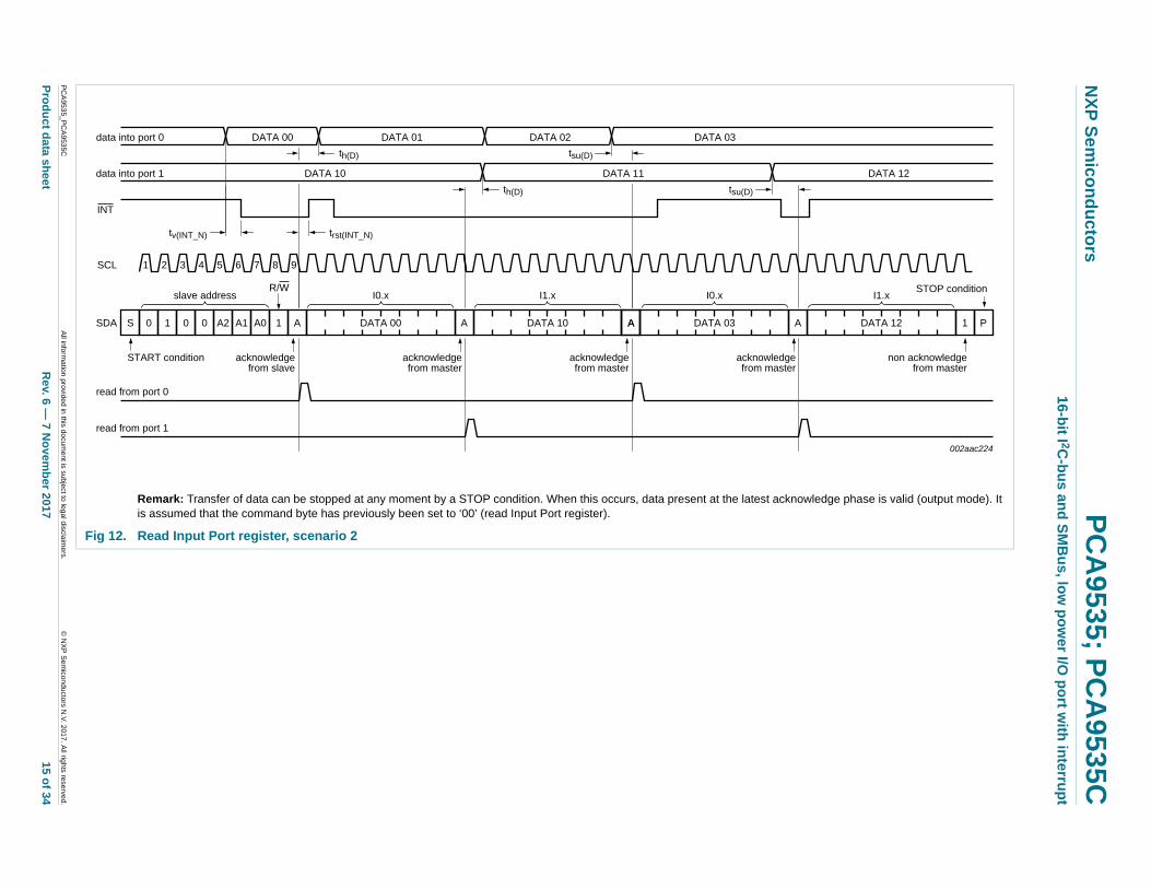
In order to read data from the PCA9535/PCA9535C, the bus master must first send the PCA9535/PCA9535C address with the least significant bit set to a logic 0 (see Figure 6 “PCA9535; PCA9535C device address”). The command byte is sent after the address and determines which register will be accessed. After a restart, the device address is sent again, but this time the least significant bit is set to a logic 1. Data from the register defined by the command byte will then be sent by the PCA9535/PCA9535C (see Figure 10, Figure 11 and Figure 12). Data is clocked into the register on the falling edge of the acknowledge clock pulse. After the first byte is read, additional bytes may be read but the data will now reflect the information in the other register in the pair. For example, if you read Input Port 1, then the next byte read would be Input Port 0. There is no limitation on the number of data bytes received in one read transmission but the final byte received, the bus master must not acknowledge the data.
Remark: Transfer can be stopped at any time by a STOP condition.
Fig 10. Read from register
AS
START condition R/W
acknowledgefrom slave
002aac222
A
acknowledgefrom slave
SDA
A P
acknowledgefrom master
DATA (first byte)
slave address
STOPcondition
S
(repeated)START condition
(cont.)
(cont.) 1 0 0 A2 A1 A0 1 A0
R/W
acknowledgefrom slave
slave address
at this moment master-transmitter becomes master-receiverand slave-receiver becomes slave-transmitter
NA
no acknowledgefrom master
COMMAND BYTE1 0 0 A2 A1 A00 0
data from lower or upper byte of register
LSBMSB
DATA (last byte)
data from upper or lower byte of register
LSBMSB
PCA9535_PCA9535C All information provided in this document is subject to legal disclaimers. © NXP Semiconductors N.V. 2017. All rights reserved.
Product data sheet Rev. 6 — 7 November 2017 13 of 34

xxxxxxxxxxxxxxxxxxxxx xxxxxxxxxxxxxxxxxxxxxxxxxx xxxxxxx x x x xxxxxxxxxxxxxxxxxxxxxxxxxxxxxx xxxxxxxxxxxxxxxxxxx xx xx xxxxx xxxxxxxxxxxxxxxxxxxxxxxxxxx xxxxxxxxxxxxxxxxxxx xxxxxx xxxxxxxxxxxxxxxxxxxxxxxxxxxxxxxxxxx xxxxxxxxxxxx x x xxxxxxxxxxxxxxxxxxxxx xxxxxxxxxxxxxxxxxxxxxxxxxxxxxx xxxxx xxxxxxxxxxxxxxxxxxxxxxxxxxxxxxxxxxxxxxxxxxxxxxxxxx xxxxxxxx xxxxxxxxxxxxxxxxxxxxxxxxx xxxxxxxxxxxxxxxxxxxx xxx
PC
A953
5_PC
A953
5CA
ll information
provided in this do
cument is sub
ject to legal d
isclaimers.
© N
XP
Se
micon
ductors N.V
. 2017. All rig
hts reserved.
Pro
du
ct data sh
eetR
ev. 6 —
7 No
vemb
er 2017 14 o
f 34
NX
P S
emico
nd
ucto
rsP
CA
9535; PC
A9535C
16-b
it I 2C-b
us an
d S
MB
us
, low
po
we
r I/O p
ort w
ith in
terru
pt
dge phase is valid (output mode). It
002aac223
P
STOP condition
1
I1.x
non acknowledgefrom master
6 5 4 3 2 1 0
Remark: Transfer of data can be stopped at any moment by a STOP condition. When this occurs, data present at the latest acknowleis assumed that the command byte has previously been set to ‘00’ (read Input Port register).
Fig 11. Read Input Port register, scenario 1
1 0 0 A2 A1 A0 1 AS 0
START condition
R/W
acknowledgefrom slave
A
SCL
SDA A
read from port 0
987654321
I0.xslave address
acknowledgefrom master
A
I1.x
acknowledgefrom master
A
I0.x
acknowledgefrom master
data into port 0
read from port 1
data into port 1
INT
6 5 4 3 2 1 07 6 5 4 3 2 1 07 6 5 4 3 2 1 07 7
INT
tv(INT_N) trst(INT_N)
xxxxxxxxxxxxxxxxxxxxx xxxxxxxxxxxxxxxxxxxxxxxxxx xxxxxxx x x x xxxxxxxxxxxxxxxxxxxxxxxxxxxxxx xxxxxxxxxxxxxxxxxxx xx xx xxxxx xxxxxxxxxxxxxxxxxxxxxxxxxxx xxxxxxxxxxxxxxxxxxx xxxxxx xxxxxxxxxxxxxxxxxxxxxxxxxxxxxxxxxxx xxxxxxxxxxxx x x xxxxxxxxxxxxxxxxxxxxx xxxxxxxxxxxxxxxxxxxxxxxxxxxxxx xxxxx xxxxxxxxxxxxxxxxxxxxxxxxxxxxxxxxxxxxxxxxxxxxxxxxxx xxxxxxxx xxxxxxxxxxxxxxxxxxxxxxxxx xxxxxxxxxxxxxxxxxxxx xxx
PC
A953
5_PC
A953
5CA
ll information
provided in this do
cument is sub
ject to legal d
isclaimers.
© N
XP
Se
micon
ductors N.V
. 2017. All rig
hts reserved.
Pro
du
ct data sh
eetR
ev. 6 —
7 No
vemb
er 2017 15 o
f 34
NX
P S
emico
nd
ucto
rsP
CA
9535; PC
A9535C
16-b
it I 2C-b
us an
d S
MB
us
, low
po
we
r I/O p
ort w
ith in
terru
pt
dge phase is valid (output mode). It
002aac224
P
STOP condition
1
I1.x
non acknowledgefrom master
DATA 12
DATA 12
Remark: Transfer of data can be stopped at any moment by a STOP condition. When this occurs, data present at the latest acknowleis assumed that the command byte has previously been set to ‘00’ (read Input Port register).
Fig 12. Read Input Port register, scenario 2
1 0 0 A2 A1 A0 1 AS 0
START condition
R/W
acknowledgefrom slave
A
SCL
SDA A
read from port 0
987654321
I0.xslave address
acknowledgefrom master
A
I1.x
acknowledgefrom master
A
I0.x
acknowledgefrom master
data into port 0
read from port 1
data into port 1
INT
tv(INT_N) trst(INT_N)
DATA 00 DATA 10 DATA 03
DATA 00 DATA 01
th(D)
th(D)
DATA 02
tsu(D)
DATA 03
tsu(D)
DATA 10 DATA 11

NXP Semiconductors PCA9535; PCA9535C16-bit I2C-bus and SMBus, low power I/O port with interrupt
6.5.3 Interrupt output
The open-drain interrupt output is activated when one of the port pins change state and the pin is configured as an input. The interrupt is deactivated when the input returns to its previous state or the Input Port register is read (see Figure 11). A pin configured as an output cannot cause an interrupt. Since each 8-bit port is read independently, the interrupt caused by Port 0 will not be cleared by a read of Port 1 or the other way around.
Remark: Changing an I/O from an output to an input may cause a false interrupt to occur if the state of the pin does not match the contents of the Input Port register.
7. Characteristics of the I2C-bus
The I2C-bus is for 2-way, 2-line communication between different ICs or modules. The two lines are a serial data line (SDA) and a serial clock line (SCL). Both lines must be connected to a positive supply via a pull-up resistor when connected to the output stages of a device. Data transfer may be initiated only when the bus is not busy.
7.1 Bit transfer
One data bit is transferred during each clock pulse. The data on the SDA line must remain stable during the HIGH period of the clock pulse as changes in the data line at this time will be interpreted as control signals (see Figure 13).
7.1.1 START and STOP conditions
Both data and clock lines remain HIGH when the bus is not busy. A HIGH-to-LOW transition of the data line while the clock is HIGH is defined as the START condition (S). A LOW-to-HIGH transition of the data line while the clock is HIGH is defined as the STOP condition (P) (see Figure 14).
Fig 13. Bit transfer
mba607
data linestable;
data valid
changeof dataallowed
SDA
SCL
Fig 14. Definition of START and STOP conditions
mba608
SDA
SCLP
STOP condition
S
START condition
PCA9535_PCA9535C All information provided in this document is subject to legal disclaimers. © NXP Semiconductors N.V. 2017. All rights reserved.
Product data sheet Rev. 6 — 7 November 2017 16 of 34

NXP Semiconductors PCA9535; PCA9535C16-bit I2C-bus and SMBus, low power I/O port with interrupt
7.2 System configuration
A device generating a message is a ‘transmitter’; a device receiving is the ‘receiver’. The device that controls the message is the ‘master’ and the devices which are controlled by the master are the ‘slaves’ (see Figure 15).
7.3 Acknowledge
The number of data bytes transferred between the START and the STOP conditions from transmitter to receiver is not limited. Each byte of eight bits is followed by one acknowledge bit. The acknowledge bit is a HIGH level put on the bus by the transmitter, whereas the master generates an extra acknowledge related clock pulse.
A slave receiver which is addressed must generate an acknowledge after the reception of each byte. Also a master must generate an acknowledge after the reception of each byte that has been clocked out of the slave transmitter. The device that acknowledges has to pull down the SDA line during the acknowledge clock pulse, so that the SDA line is stable LOW during the HIGH period of the acknowledge related clock pulse; set-up time and hold time must be taken into account.
A master receiver must signal an end of data to the transmitter by not generating an acknowledge on the last byte that has been clocked out of the slave. In this event, the transmitter must leave the data line HIGH to enable the master to generate a STOP condition.
Fig 15. System configuration
002aaa966
MASTERTRANSMITTER/
RECEIVER
SLAVERECEIVER
SLAVETRANSMITTER/
RECEIVER
MASTERTRANSMITTER
MASTERTRANSMITTER/
RECEIVER
SDA
SCL
I2C-BUSMULTIPLEXER
SLAVE
Fig 16. Acknowledgement on the I2C-bus
002aaa987
S
STARTcondition
9821
clock pulse foracknowledgement
not acknowledge
acknowledge
data outputby transmitter
data outputby receiver
SCL from master
PCA9535_PCA9535C All information provided in this document is subject to legal disclaimers. © NXP Semiconductors N.V. 2017. All rights reserved.
Product data sheet Rev. 6 — 7 November 2017 17 of 34
NXP Semiconductors PCA9535; PCA9535C16-bit I2C-bus and SMBus, low power I/O port with interrupt
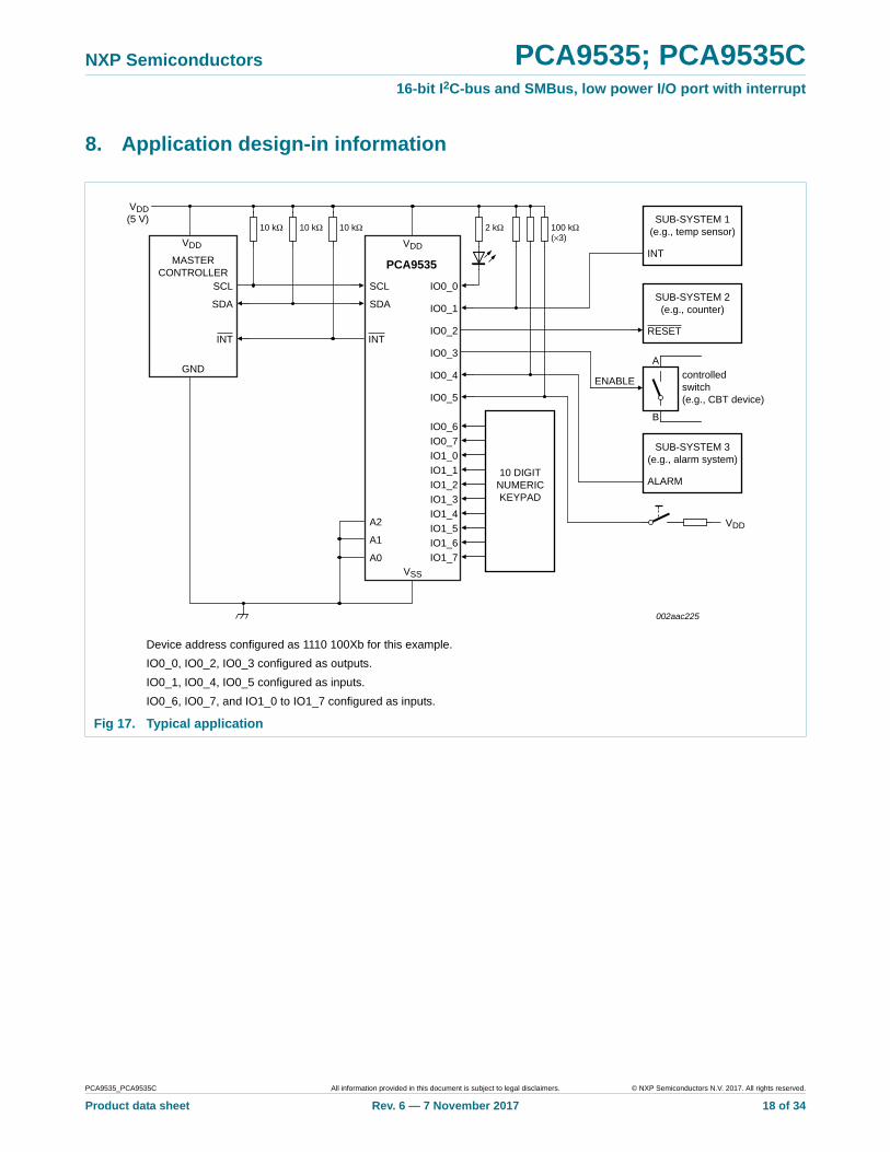
8. Application design-in information
Device address configured as 1110 100Xb for this example.
IO0_0, IO0_2, IO0_3 configured as outputs.
IO0_1, IO0_4, IO0_5 configured as inputs.
IO0_6, IO0_7, and IO1_0 to IO1_7 configured as inputs.
Fig 17. Typical application
PCA9535
IO0_0
IO0_1
SCL
SDA
VDD(5 V)
MASTERCONTROLLER
SCL
SDA
INTIO0_2
VDD
A2
A1
A0
VDD
GND
INT
10 kΩSUB-SYSTEM 1
(e.g., temp sensor)
IO0_3
INT
SUB-SYSTEM 2(e.g., counter)
RESET
controlledswitch(e.g., CBT device)
VDD
A
B
ENABLE
SUB-SYSTEM 3(e.g., alarm system)
ALARM
IO0_4
IO0_5
IO0_6
10 DIGITNUMERICKEYPAD
VSS
002aac225
10 kΩ10 kΩ 2 kΩ 100 kΩ(×3)
IO0_7IO1_0IO1_1IO1_2IO1_3IO1_4IO1_5IO1_6IO1_7
PCA9535_PCA9535C All information provided in this document is subject to legal disclaimers. © NXP Semiconductors N.V. 2017. All rights reserved.
Product data sheet Rev. 6 — 7 November 2017 18 of 34

NXP Semiconductors PCA9535; PCA9535C16-bit I2C-bus and SMBus, low power I/O port with interrupt
8.1 Minimizing IDD when the I/Os are used to control LEDs
When the PCA9535 I/Os are used to control LEDs, they are normally connected to VDD through a resistor as shown in Figure 17. Since the LED acts as a diode, when the LED is off the I/O VI is about 1.2 V less than VDD. The supply current, IDD, increases as VI becomes lower than VDD.
Designs needing to minimize current consumption, such as battery power applications, should consider maintaining the I/O pins greater than or equal to VDD when the LED is off. Figure 18 shows a high value resistor in parallel with the LED. Figure 19 shows VDD less than the LED supply voltage by at least 1.2 V. Both of these methods maintain the I/O VI at or above VDD and prevents additional supply current consumption when the LED is off.
This concern does not occur in the case of PCA9535C because the I/O pins are open-drain.
9. Limiting values
Fig 18. High value resistor in parallel with the LED
Fig 19. Device supplied by a lower voltage
002aac189
LEDVDD
LEDn
100 kΩ
VDD
002aac190
LEDVDD
LEDn
3.3 V 5 V
Table 13. Limiting valuesIn accordance with the Absolute Maximum Rating System (IEC 60134).
Symbol Parameter Conditions Min Max Unit
VDD supply voltage 0.5 +6.0 V
VI/O voltage on an input/output pin VSS 0.5 6 V
IO output current on an I/O pin - 50 mA
II input current - 20 mA
IDD supply current - 160 mA
ISS ground supply current - 200 mA
Ptot total power dissipation - 200 mW
Tstg storage temperature 65 +150 C
Tamb ambient temperature operating 40 +85 C
PCA9535_PCA9535C All information provided in this document is subject to legal disclaimers. © NXP Semiconductors N.V. 2017. All rights reserved.
Product data sheet Rev. 6 — 7 November 2017 19 of 34

NXP Semiconductors PCA9535; PCA9535C16-bit I2C-bus and SMBus, low power I/O port with interrupt
10. Static characteristics
[1] VDD must be lowered to 0.2 V for at least 5 s in order to reset part.
Table 14. Static characteristicsVDD = 2.3 V to 5.5 V; VSS = 0 V; Tamb = 40 C to +85 C; unless otherwise specified.
Symbol Parameter Conditions Min Typ Max Unit
Supplies
VDD supply voltage 2.3 - 5.5 V
IDD supply current Operating mode; VDD = 5.5 V; no load; fSCL = 100 kHz; I/O = inputs
- 135 200 A
Istb standby current Standby mode; VDD = 5.5 V; no load; VI = VSS; fSCL = 0 kHz; I/O = inputs
- 0.25 1 A
Standby mode; VDD = 5.5 V; no load; VI = VDD; fSCL = 0 kHz; I/O = inputs
- 0.25 1 A
VPOR power-on reset voltage[1] no load; VI = VDD or VSS - 1.7 2.2 V
Input SCL; input/output SDA
VIL LOW-level input voltage 0.5 - +0.3VDD V
VIH HIGH-level input voltage 0.7VDD - 5.5 V
IOL LOW-level output current VOL = 0.4 V 3 - - mA
IL leakage current VI = VDD = VSS 1 - +1 A
Ci input capacitance VI = VSS - 6 10 pF
I/Os
VIL LOW-level input voltage 0.5 - +0.3VDD V
VIH HIGH-level input voltage 0.7VDD - 5.5 V
IOL LOW-level output current VDD = 2.3 V to 5.5 V; VOL = 0.5 V [2] 8 10 - mA
VDD = 2.3 V to 5.5 V; VOL = 0.7 V [2] 10 14 - mA
VOH HIGH-level output voltage PCA9535 only
IOH = 8 mA; VDD = 2.3 V [3] 1.8 - - V
IOH = 10 mA; VDD = 2.3 V [3] 1.7 - - V
IOH = 8 mA; VDD = 3.0 V [3] 2.6 - - V
IOH = 10 mA; VDD = 3.0 V [3] 2.5 - - V
IOH = 8 mA; VDD = 4.75 V [3] 4.1 - - V
IOH = 10 mA; VDD = 4.75 V [3] 4.0 - - V
ILIH HIGH-level input leakage current VDD = 5.5 V; VI = VDD - - 1 A
ILIL LOW-level input leakage current VDD = 5.5 V; VI = VSS - - 1 A
Ci input capacitance - 3.7 5 pF
Co output capacitance - 3.7 5 pF
Interrupt INT
IOL LOW-level output current VOL = 0.4 V 3 - - mA
Select inputs A0, A1, A2
VIL LOW-level input voltage 0.5 - +0.3VDD V
VIH HIGH-level input voltage 0.7VDD - 5.5 V
ILI input leakage current 1 - +1 A
PCA9535_PCA9535C All information provided in this document is subject to legal disclaimers. © NXP Semiconductors N.V. 2017. All rights reserved.
Product data sheet Rev. 6 — 7 November 2017 20 of 34

NXP Semiconductors PCA9535; PCA9535C16-bit I2C-bus and SMBus, low power I/O port with interrupt
[2] Each I/O must be externally limited to a maximum of 25 mA and each octal (IO0_0 to IO0_7 and IO1_0 to IO1_7) must be limited to a maximum current of 100 mA for a device total of 200 mA.
[3] The total current sourced by all I/Os must be limited to 160 mA. PCA9535C does not source current and does not have the VOH specification.
11. Dynamic characteristics
[1] tVD;ACK = time for acknowledgement signal from SCL LOW to SDA (out) LOW.
[2] tVD;DAT = minimum time for SDA data out to be valid following SCL LOW.
[3] Cb = total capacitance of one bus line in pF.
[4] tv(Q) measured from 0.7VDD on SCL to 50 % I/O output (PCA9535). For PCA9535C, use load circuit shown in Figure 24 and measure from 0.7VDD on SCL to 30 % I/O output.
Table 15. Dynamic characteristics
Symbol Parameter Conditions Standard-mode I2C-bus
Fast-mode I2C-bus Unit
Min Max Min Max
fSCL SCL clock frequency 0 100 0 400 kHz
tBUF bus free time between a STOP and START condition
4.7 - 1.3 - s
tHD;STA hold time (repeated) START condition 4.0 - 0.6 - s
tSU;STA set-up time for a repeated START condition
4.7 - 0.6 - s
tSU;STO set-up time for STOP condition 4.0 - 0.6 - s
tVD;ACK data valid acknowledge time [1] 0.3 3.45 0.1 0.9 s
tHD;DAT data hold time 0 - 0 - ns
tVD;DAT data valid time [2] 300 - 50 - ns
tSU;DAT data set-up time 250 - 100 - ns
tLOW LOW period of the SCL clock 4.7 - 1.3 - s
tHIGH HIGH period of the SCL clock 4.0 - 0.6 - s
tf fall time of both SDA and SCL signals - 300 20 + 0.1Cb[3] 300 ns
tr rise time of both SDA and SCL signals - 1000 20 + 0.1Cb[3] 300 ns
tSP pulse width of spikes that must be suppressed by the input filter
- 50 - 50 ns
Port timing
tv(Q) data output valid time [4] - 200 - 200 ns
tsu(D) data input set-up time 150 - 150 - ns
th(D) data input hold time 1 - 1 - s
Interrupt timing
tv(INT_N) valid time on pin INT - 4 - 4 s
trst(INT_N) reset time on pin INT - 4 - 4 s
PCA9535_PCA9535C All information provided in this document is subject to legal disclaimers. © NXP Semiconductors N.V. 2017. All rights reserved.
Product data sheet Rev. 6 — 7 November 2017 21 of 34
NXP Semiconductors PCA9535; PCA9535C16-bit I2C-bus and SMBus, low power I/O port with interrupt
Fig 20. Definition of timing on the I2C-bus
tSPtBUF
tHD;STAPP S
tLOW
tr
tHD;DAT
tf
tHIGH tSU;DATtSU;STA
Sr
tHD;STA
tSU;STO
SDA
SCL
002aaa986
0.7 × VDD
0.3 × VDD
0.7 × VDD
0.3 × VDD
Rise and fall times refer to VIL and VIH.
Fig 21. I2C-bus timing diagram
002aab175
protocolSTART
condition(S)
bit 7MSB(A7)
bit 6(A6)
bit 0(R/W)
acknowledge(A)
STOPcondition
(P)
SCL
SDA
tHD;STA tSU;DAT tHD;DAT
tftBUF
tSU;STA tLOW tHIGH
tVD;ACK tSU;STO
1 / fSCL
tr
tVD;DAT
0.3 × VDD
0.7 × VDD
0.3 × VDD
0.7 × VDD
Fig 22. tv(Q) timing
tv(Q)
SCL
002aad327
IOn
tv(Q)
SCL
IOn
PCA9535_PCA9535C All information provided in this document is subject to legal disclaimers. © NXP Semiconductors N.V. 2017. All rights reserved.
Product data sheet Rev. 6 — 7 November 2017 22 of 34

NXP Semiconductors PCA9535; PCA9535C16-bit I2C-bus and SMBus, low power I/O port with interrupt
12. Test information
RL = load resistor.
CL = load capacitance includes jig and probe capacitance.
RT = termination resistance should be equal to the output impedance of Zo of the pulse generators.
Fig 23. Test circuitry for switching times
Fig 24. Load circuit
PULSEGENERATOR
VO
CL50 pF
RL500 Ω
002aab284
RT
VI
VDD
DUT
VDDopenGND
CL50 pF
002aac226
RL500 Ω
from output under test2VDDopenGND
S1RL
500 Ω
PCA9535_PCA9535C All information provided in this document is subject to legal disclaimers. © NXP Semiconductors N.V. 2017. All rights reserved.
Product data sheet Rev. 6 — 7 November 2017 23 of 34

NXP Semiconductors PCA9535; PCA9535C16-bit I2C-bus and SMBus, low power I/O port with interrupt
13. Package outline
Fig 25. Package outline SOT137-1 (SO24)
UNITA
max. A1 A2 A3 bp c D (1) E (1) (1)e HE L Lp Q Zywv θ
REFERENCESOUTLINEVERSION
EUROPEANPROJECTION ISSUE DATE
IEC JEDEC JEITA
mm
inches
2.65 0.30.1
2.452.25
0.490.36
0.320.23
15.615.2
7.67.4
1.2710.6510.00
1.11.0
0.90.4 8
0
o
o
0.25 0.1
DIMENSIONS (inch dimensions are derived from the original mm dimensions)
Note
1. Plastic or metal protrusions of 0.15 mm (0.006 inch) maximum per side are not included.
1.10.4
SOT137-1
X
12
24
w M
θ
AA1
A2
bp
D
HE
Lp
Q
detail X
E
Z
c
L
v M A
13
(A )3
A
y
0.25
075E05 MS-013
pin 1 index
0.1 0.0120.004
0.0960.089
0.0190.014
0.0130.009
0.610.60
0.300.29
0.05
1.4
0.0550.4190.394
0.0430.039
0.0350.016
0.01
0.25
0.01 0.0040.0430.016
0.01
e
1
0 5 10 mm
scale
SO24: plastic small outline package; 24 leads; body width 7.5 mm SOT137-1
99-12-2703-02-19
PCA9535_PCA9535C All information provided in this document is subject to legal disclaimers. © NXP Semiconductors N.V. 2017. All rights reserved.
Product data sheet Rev. 6 — 7 November 2017 24 of 34

NXP Semiconductors PCA9535; PCA9535C16-bit I2C-bus and SMBus, low power I/O port with interrupt
Fig 26. Package outline SOT355-1 (TSSOP24)
UNIT A1 A2 A3 bp c D(1) E(2) (1)e HE L Lp Q Zywv θ
REFERENCESOUTLINEVERSION
EUROPEANPROJECTION ISSUE DATE
IEC JEDEC JEITA
mm 0.150.05
0.950.80
0.300.19
0.20.1
7.97.7
4.54.3
0.656.66.2
0.40.3
80
o
o0.13 0.10.21
DIMENSIONS (mm are the original dimensions)
Notes
1. Plastic or metal protrusions of 0.15 mm maximum per side are not included.
2. Plastic interlead protrusions of 0.25 mm maximum per side are not included.
0.750.50
SOT355-1 MO-15399-12-2703-02-19
0.250.50.2
w Mbp
Z
e
1 12
24 13
pin 1 index
θ
AA1
A2
Lp
Q
detail X
L
(A )3
HE
E
c
v M A
XAD
y
0 2.5 5 mm
scale
TSSOP24: plastic thin shrink small outline package; 24 leads; body width 4.4 mm SOT355-1
Amax.
1.1
PCA9535_PCA9535C All information provided in this document is subject to legal disclaimers. © NXP Semiconductors N.V. 2017. All rights reserved.
Product data sheet Rev. 6 — 7 November 2017 25 of 34

NXP Semiconductors PCA9535; PCA9535C16-bit I2C-bus and SMBus, low power I/O port with interrupt
Fig 27. Package outline SOT616-1 (HVQFN24)
0.51 0.2
A1 EhbUNIT ye
REFERENCESOUTLINEVERSION
EUROPEANPROJECTION ISSUE DATE
IEC JEDEC JEITA
mm 4.13.9
Dh
2.251.95
y1
4.13.9
2.251.95
e1
2.5
e2
2.50.300.18
c
0.050.00
0.05 0.1
DIMENSIONS (mm are the original dimensions)
SOT616-1 MO-220 - - -- - -
0.50.3
L
0.1
v
0.05
w
0 2.5 5 mm
scale
SOT616-1HVQFN24: plastic thermal enhanced very thin quad flat package; no leads;24 terminals; body 4 x 4 x 0.85 mm
A(1)
max.
AA1
c
detail X
yy1 Ce
L
Eh
Dh
e
e1
b7 12
24 19
18
136
1
X
D
E
C
B A
e2
01-08-0802-10-22
terminal 1index area
terminal 1index area
ACC
Bv M
w M
1/2 e
1/2 e
E(1)
Note
1. Plastic or metal protrusions of 0.075 mm maximum per side are not included.
D(1)
PCA9535_PCA9535C All information provided in this document is subject to legal disclaimers. © NXP Semiconductors N.V. 2017. All rights reserved.
Product data sheet Rev. 6 — 7 November 2017 26 of 34

NXP Semiconductors PCA9535; PCA9535C16-bit I2C-bus and SMBus, low power I/O port with interrupt
Fig 28. Package outline SOT994-1 (HWQFN24)
REFERENCESOUTLINEVERSION
EUROPEANPROJECTION
ISSUE DATEIEC JEDEC JEITA
SOT994-1 - - -MO-220- - -
SOT994-1
07-02-0707-03-03
Note1. Plastic or metal protrusions of 0.075 mm maximum per side are not included.
UNIT A(1)
max
mm 0.8 0.050.00
0.300.18
4.13.9
2.251.95
4.13.9
2.251.95 2.5 2.5 0.1
A1
DIMENSIONS (mm are the original dimensions)
HWQFN24: plastic thermal enhanced very very thin quad flat package; no leads;24 terminals; body 4 x 4 x 0.75 mm
0 2.5 5 mm
scale
b c
0.2
D(1) Dh E(1) Eh e
0.5
e1 e2 L
0.50.3
v w
0.05
y
0.05
y1
0.1
B A
terminal 1index area
E
D
detail X
A
A1c
b
e2
e1
e
e
1/2 e
1/2 e
AC B∅ v M
C∅ w M
terminal 1index area
613
127
18
24 19
1
L
Eh
Dh
C
yCy1
X
PCA9535_PCA9535C All information provided in this document is subject to legal disclaimers. © NXP Semiconductors N.V. 2017. All rights reserved.
Product data sheet Rev. 6 — 7 November 2017 27 of 34

NXP Semiconductors PCA9535; PCA9535C16-bit I2C-bus and SMBus, low power I/O port with interrupt
14. Handling information
Inputs and outputs are protected against electrostatic discharge in normal handling. However, to be completely safe you must take normal precautions appropriate to handling integrated circuits.
15. Soldering of SMD packages
This text provides a very brief insight into a complex technology. A more in-depth account of soldering ICs can be found in Application Note AN10365 “Surface mount reflow soldering description”.
15.1 Introduction to soldering
Soldering is one of the most common methods through which packages are attached to Printed Circuit Boards (PCBs), to form electrical circuits. The soldered joint provides both the mechanical and the electrical connection. There is no single soldering method that is ideal for all IC packages. Wave soldering is often preferred when through-hole and Surface Mount Devices (SMDs) are mixed on one printed wiring board; however, it is not suitable for fine pitch SMDs. Reflow soldering is ideal for the small pitches and high densities that come with increased miniaturization.
15.2 Wave and reflow soldering
Wave soldering is a joining technology in which the joints are made by solder coming from a standing wave of liquid solder. The wave soldering process is suitable for the following:
• Through-hole components
• Leaded or leadless SMDs, which are glued to the surface of the printed circuit board
Not all SMDs can be wave soldered. Packages with solder balls, and some leadless packages which have solder lands underneath the body, cannot be wave soldered. Also, leaded SMDs with leads having a pitch smaller than ~0.6 mm cannot be wave soldered, due to an increased probability of bridging.
The reflow soldering process involves applying solder paste to a board, followed by component placement and exposure to a temperature profile. Leaded packages, packages with solder balls, and leadless packages are all reflow solderable.
Key characteristics in both wave and reflow soldering are:
• Board specifications, including the board finish, solder masks and vias
• Package footprints, including solder thieves and orientation
• The moisture sensitivity level of the packages
• Package placement
• Inspection and repair
• Lead-free soldering versus SnPb soldering
15.3 Wave soldering
Key characteristics in wave soldering are:
PCA9535_PCA9535C All information provided in this document is subject to legal disclaimers. © NXP Semiconductors N.V. 2017. All rights reserved.
Product data sheet Rev. 6 — 7 November 2017 28 of 34

NXP Semiconductors PCA9535; PCA9535C16-bit I2C-bus and SMBus, low power I/O port with interrupt
• Process issues, such as application of adhesive and flux, clinching of leads, board transport, the solder wave parameters, and the time during which components are exposed to the wave
• Solder bath specifications, including temperature and impurities
15.4 Reflow soldering
Key characteristics in reflow soldering are:
• Lead-free versus SnPb soldering; note that a lead-free reflow process usually leads to higher minimum peak temperatures (see Figure 29) than a SnPb process, thus reducing the process window
• Solder paste printing issues including smearing, release, and adjusting the process window for a mix of large and small components on one board
• Reflow temperature profile; this profile includes preheat, reflow (in which the board is heated to the peak temperature) and cooling down. It is imperative that the peak temperature is high enough for the solder to make reliable solder joints (a solder paste characteristic). In addition, the peak temperature must be low enough that the packages and/or boards are not damaged. The peak temperature of the package depends on package thickness and volume and is classified in accordance with Table 16 and 17
Moisture sensitivity precautions, as indicated on the packing, must be respected at all times.
Studies have shown that small packages reach higher temperatures during reflow soldering, see Figure 29.
Table 16. SnPb eutectic process (from J-STD-020C)
Package thickness (mm) Package reflow temperature (C)
Volume (mm3)
< 350 350
< 2.5 235 220
2.5 220 220
Table 17. Lead-free process (from J-STD-020C)
Package thickness (mm) Package reflow temperature (C)
Volume (mm3)
< 350 350 to 2000 > 2000
< 1.6 260 260 260
1.6 to 2.5 260 250 245
> 2.5 250 245 245
PCA9535_PCA9535C All information provided in this document is subject to legal disclaimers. © NXP Semiconductors N.V. 2017. All rights reserved.
Product data sheet Rev. 6 — 7 November 2017 29 of 34

NXP Semiconductors PCA9535; PCA9535C16-bit I2C-bus and SMBus, low power I/O port with interrupt
For further information on temperature profiles, refer to Application Note AN10365 “Surface mount reflow soldering description”.
16. Abbreviations
MSL: Moisture Sensitivity Level
Fig 29. Temperature profiles for large and small components
001aac844
temperature
time
minimum peak temperature= minimum soldering temperature
maximum peak temperature= MSL limit, damage level
peak temperature
Table 18. Abbreviations
Acronym Description
ACPI Advanced Configuration and Power Interface
CBT Cross Bar Technology
CDM Charged-Device Model
CMOS Complementary Metal-Oxide Semiconductor
DUT Device Under Test
ESD ElectroStatic Discharge
FET Field-Effect Transistor
GPIO General Purpose Input/Output
HBM Human Body Model
I/O Input/Output
I2C-bus Inter-Integrated Circuit bus
IC Integrated Circuit
LED Light Emitting Diode
MM Machine Model
PCB Printed-Circuit Board
SMBus System Management Bus
PCA9535_PCA9535C All information provided in this document is subject to legal disclaimers. © NXP Semiconductors N.V. 2017. All rights reserved.
Product data sheet Rev. 6 — 7 November 2017 30 of 34
NXP Semiconductors PCA9535; PCA9535C16-bit I2C-bus and SMBus, low power I/O port with interrupt
17. Revision history
Table 19. Revision history
Document ID Release date Data sheet status Change notice Supersedes
PCA9535_PCA9535C v.6 20171107 Product data sheet 201710002I PCA9535_PCA9535C_5
Modifications: • Table 14 “Static characteristics”: Corrected VPOR typ and max limit
• Added Section 3.1 “Ordering options”
PCA9535_PCA9535C_5 20080915 Product data sheet - PCA9535_PCA9535C_4
Modifications: • Table 3 “Pin description”: Table note [1] re-written; added its reference at port 1input/output
PCA9535_PCA9535C_4 20080731 Product data sheet - PCA9535_PCA9535C_3
PCA9535_PCA9535C_3 20071004 Product data sheet - PCA9535_2
PCA9535_2 (9397 750 12896)
20040930 Product data sheet - PCA9535_1
PCA9535_1 (9397 750 11681)
20030627 Product data 853-2430 30019 of 11 June 2003
-
PCA9535_PCA9535C All information provided in this document is subject to legal disclaimers. © NXP Semiconductors N.V. 2017. All rights reserved.
Product data sheet Rev. 6 — 7 November 2017 31 of 34

NXP Semiconductors PCA9535; PCA9535C16-bit I2C-bus and SMBus, low power I/O port with interrupt
18. Legal information
18.1 Data sheet status
[1] Please consult the most recently issued document before initiating or completing a design.
[2] The term ‘short data sheet’ is explained in section “Definitions”.
[3] The product status of device(s) described in this document may have changed since this document was published and may differ in case of multiple devices. The latest product status information is available on the Internet at URL http://www.nxp.com.
18.2 Definitions
Draft — The document is a draft version only. The content is still under internal review and subject to formal approval, which may result in modifications or additions. NXP Semiconductors does not give any representations or warranties as to the accuracy or completeness of information included herein and shall have no liability for the consequences of use of such information.
Short data sheet — A short data sheet is an extract from a full data sheet with the same product type number(s) and title. A short data sheet is intended for quick reference only and should not be relied upon to contain detailed and full information. For detailed and full information see the relevant full data sheet, which is available on request via the local NXP Semiconductors sales office. In case of any inconsistency or conflict with the short data sheet, the full data sheet shall prevail.
Product specification — The information and data provided in a Product data sheet shall define the specification of the product as agreed between NXP Semiconductors and its customer, unless NXP Semiconductors and customer have explicitly agreed otherwise in writing. In no event however, shall an agreement be valid in which the NXP Semiconductors product is deemed to offer functions and qualities beyond those described in the Product data sheet.
18.3 Disclaimers
Limited warranty and liability — Information in this document is believed to be accurate and reliable. However, NXP Semiconductors does not give any representations or warranties, expressed or implied, as to the accuracy or completeness of such information and shall have no liability for the consequences of use of such information. NXP Semiconductors takes no responsibility for the content in this document if provided by an information source outside of NXP Semiconductors.
In no event shall NXP Semiconductors be liable for any indirect, incidental, punitive, special or consequential damages (including - without limitation - lost profits, lost savings, business interruption, costs related to the removal or replacement of any products or rework charges) whether or not such damages are based on tort (including negligence), warranty, breach of contract or any other legal theory.
Notwithstanding any damages that customer might incur for any reason whatsoever, NXP Semiconductors’ aggregate and cumulative liability towards customer for the products described herein shall be limited in accordance with the Terms and conditions of commercial sale of NXP Semiconductors.
Right to make changes — NXP Semiconductors reserves the right to make changes to information published in this document, including without limitation specifications and product descriptions, at any time and without notice. This document supersedes and replaces all information supplied prior to the publication hereof.
Suitability for use — NXP Semiconductors products are not designed, authorized or warranted to be suitable for use in life support, life-critical or safety-critical systems or equipment, nor in applications where failure or malfunction of an NXP Semiconductors product can reasonably be expected to result in personal injury, death or severe property or environmental damage. NXP Semiconductors and its suppliers accept no liability for inclusion and/or use of NXP Semiconductors products in such equipment or applications and therefore such inclusion and/or use is at the customer’s own risk.
Applications — Applications that are described herein for any of these products are for illustrative purposes only. NXP Semiconductors makes no representation or warranty that such applications will be suitable for the specified use without further testing or modification.
Customers are responsible for the design and operation of their applications and products using NXP Semiconductors products, and NXP Semiconductors accepts no liability for any assistance with applications or customer product design. It is customer’s sole responsibility to determine whether the NXP Semiconductors product is suitable and fit for the customer’s applications and products planned, as well as for the planned application and use of customer’s third party customer(s). Customers should provide appropriate design and operating safeguards to minimize the risks associated with their applications and products.
NXP Semiconductors does not accept any liability related to any default, damage, costs or problem which is based on any weakness or default in the customer’s applications or products, or the application or use by customer’s third party customer(s). Customer is responsible for doing all necessary testing for the customer’s applications and products using NXP Semiconductors products in order to avoid a default of the applications and the products or of the application or use by customer’s third party customer(s). NXP does not accept any liability in this respect.
Limiting values — Stress above one or more limiting values (as defined in the Absolute Maximum Ratings System of IEC 60134) will cause permanent damage to the device. Limiting values are stress ratings only and (proper) operation of the device at these or any other conditions above those given in the Recommended operating conditions section (if present) or the Characteristics sections of this document is not warranted. Constant or repeated exposure to limiting values will permanently and irreversibly affect the quality and reliability of the device.
Terms and conditions of commercial sale — NXP Semiconductors products are sold subject to the general terms and conditions of commercial sale, as published at http://www.nxp.com/profile/terms, unless otherwise agreed in a valid written individual agreement. In case an individual agreement is concluded only the terms and conditions of the respective agreement shall apply. NXP Semiconductors hereby expressly objects to applying the customer’s general terms and conditions with regard to the purchase of NXP Semiconductors products by customer.
No offer to sell or license — Nothing in this document may be interpreted or construed as an offer to sell products that is open for acceptance or the grant, conveyance or implication of any license under any copyrights, patents or other industrial or intellectual property rights.
Document status[1][2] Product status[3] Definition
Objective [short] data sheet Development This document contains data from the objective specification for product development.
Preliminary [short] data sheet Qualification This document contains data from the preliminary specification.
Product [short] data sheet Production This document contains the product specification.
PCA9535_PCA9535C All information provided in this document is subject to legal disclaimers. © NXP Semiconductors N.V. 2017. All rights reserved.
Product data sheet Rev. 6 — 7 November 2017 32 of 34

NXP Semiconductors PCA9535; PCA9535C16-bit I2C-bus and SMBus, low power I/O port with interrupt
Export control — This document as well as the item(s) described herein may be subject to export control regulations. Export might require a prior authorization from competent authorities.
Quick reference data — The Quick reference data is an extract of the product data given in the Limiting values and Characteristics sections of this document, and as such is not complete, exhaustive or legally binding.
Non-automotive qualified products — Unless this data sheet expressly states that this specific NXP Semiconductors product is automotive qualified, the product is not suitable for automotive use. It is neither qualified nor tested in accordance with automotive testing or application requirements. NXP Semiconductors accepts no liability for inclusion and/or use of non-automotive qualified products in automotive equipment or applications.
In the event that customer uses the product for design-in and use in automotive applications to automotive specifications and standards, customer (a) shall use the product without NXP Semiconductors’ warranty of the product for such automotive applications, use and specifications, and (b)
whenever customer uses the product for automotive applications beyond NXP Semiconductors’ specifications such use shall be solely at customer’s own risk, and (c) customer fully indemnifies NXP Semiconductors for any liability, damages or failed product claims resulting from customer design and use of the product for automotive applications beyond NXP Semiconductors’ standard warranty and NXP Semiconductors’ product specifications.
Translations — A non-English (translated) version of a document is for reference only. The English version shall prevail in case of any discrepancy between the translated and English versions.
18.4 TrademarksNotice: All referenced brands, product names, service names and trademarks are the property of their respective owners.
I2C-bus — logo is a trademark of NXP Semiconductors N.V.
19. Contact information
For more information, please visit: http://www.nxp.com
For sales office addresses, please send an email to: [email protected]
PCA9535_PCA9535C All information provided in this document is subject to legal disclaimers. © NXP Semiconductors N.V. 2017. All rights reserved.
Product data sheet Rev. 6 — 7 November 2017 33 of 34

NXP Semiconductors PCA9535; PCA9535C16-bit I2C-bus and SMBus, low power I/O port with interrupt
20. Contents
1 General description . . . . . . . . . . . . . . . . . . . . . . 1
2 Features and benefits . . . . . . . . . . . . . . . . . . . . 1
3 Ordering information. . . . . . . . . . . . . . . . . . . . . 23.1 Ordering options . . . . . . . . . . . . . . . . . . . . . . . . 2
4 Block diagram . . . . . . . . . . . . . . . . . . . . . . . . . . 4
5 Pinning information. . . . . . . . . . . . . . . . . . . . . . 55.1 Pinning . . . . . . . . . . . . . . . . . . . . . . . . . . . . . . . 55.2 Pin description . . . . . . . . . . . . . . . . . . . . . . . . . 6
6 Functional description . . . . . . . . . . . . . . . . . . . 76.1 Device address. . . . . . . . . . . . . . . . . . . . . . . . . 76.2 Registers . . . . . . . . . . . . . . . . . . . . . . . . . . . . . 76.2.1 Command byte . . . . . . . . . . . . . . . . . . . . . . . . . 76.2.2 Registers 0 and 1: Input port registers . . . . . . . 86.2.3 Registers 2 and 3: Output port registers. . . . . . 86.2.4 Registers 4 and 5: Polarity Inversion registers . 86.2.5 Registers 6 and 7: Configuration registers . . . . 96.3 Power-on reset . . . . . . . . . . . . . . . . . . . . . . . . . 96.4 I/O port . . . . . . . . . . . . . . . . . . . . . . . . . . . . . . . 96.5 Bus transactions . . . . . . . . . . . . . . . . . . . . . . . 106.5.1 Writing to the port registers. . . . . . . . . . . . . . . 106.5.2 Reading the port registers . . . . . . . . . . . . . . . 136.5.3 Interrupt output . . . . . . . . . . . . . . . . . . . . . . . . 16
7 Characteristics of the I2C-bus . . . . . . . . . . . . 167.1 Bit transfer . . . . . . . . . . . . . . . . . . . . . . . . . . . 167.1.1 START and STOP conditions . . . . . . . . . . . . . 167.2 System configuration . . . . . . . . . . . . . . . . . . . 177.3 Acknowledge . . . . . . . . . . . . . . . . . . . . . . . . . 17
8 Application design-in information . . . . . . . . . 188.1 Minimizing IDD when the I/Os are used to control
LEDs. . . . . . . . . . . . . . . . . . . . . . . . . . . . . . . . 19
9 Limiting values. . . . . . . . . . . . . . . . . . . . . . . . . 19
10 Static characteristics. . . . . . . . . . . . . . . . . . . . 20
11 Dynamic characteristics . . . . . . . . . . . . . . . . . 21
12 Test information. . . . . . . . . . . . . . . . . . . . . . . . 23
13 Package outline . . . . . . . . . . . . . . . . . . . . . . . . 24
14 Handling information. . . . . . . . . . . . . . . . . . . . 28
15 Soldering of SMD packages . . . . . . . . . . . . . . 2815.1 Introduction to soldering . . . . . . . . . . . . . . . . . 2815.2 Wave and reflow soldering . . . . . . . . . . . . . . . 2815.3 Wave soldering . . . . . . . . . . . . . . . . . . . . . . . . 2815.4 Reflow soldering . . . . . . . . . . . . . . . . . . . . . . . 29
16 Abbreviations. . . . . . . . . . . . . . . . . . . . . . . . . . 30
17 Revision history. . . . . . . . . . . . . . . . . . . . . . . . 31
18 Legal information. . . . . . . . . . . . . . . . . . . . . . . 32
18.1 Data sheet status . . . . . . . . . . . . . . . . . . . . . . 3218.2 Definitions . . . . . . . . . . . . . . . . . . . . . . . . . . . 3218.3 Disclaimers . . . . . . . . . . . . . . . . . . . . . . . . . . 3218.4 Trademarks . . . . . . . . . . . . . . . . . . . . . . . . . . 33
19 Contact information . . . . . . . . . . . . . . . . . . . . 33
20 Contents. . . . . . . . . . . . . . . . . . . . . . . . . . . . . . 34
© NXP Semiconductors N.V. 2017. All rights reserved.
For more information, please visit: http://www.nxp.comFor sales office addresses, please send an email to: [email protected]
Date of release: 7 November 2017
Document identifier: PCA9535_PCA9535C
Please be aware that important notices concerning this document and the product(s)described herein, have been included in section ‘Legal information’.