pb nbpx, battery pressure monitor sensor, product brief
TRANSCRIPT

NBPxBattery pressure monitor sensorRev. 2 — 1 October 2021 Product brief
1 General description
The NBPx family consists of small QFN (4 mm x 4 mm x 1.98 mm), fully integratedbattery pressure monitoring sensors (BPMS). The NBPx BPMS solution integrates an 8-bit central processing unit (CPU) and NXP-provided firmware to create the ready-to-usepressure sensor.
The battery pressure monitoring sensors have a built in MCU and are capable of sensingthe pressure change, making a configuration-based decision, and acting on this decisionwhile providing this information to the host system.
2 Features and benefits
• Wide operating pressure range 40 – 250 kPa• Transducer measurement interfaces with low-power AFE:
– 10-bit compensated pressure sense element– 8-bit compensated internal device temperature measurement– 8-bit compensated internal device voltage measurement
• 12-entry pressure FIFO• Selectable host wake-up indications:
– fixed pressure threshold– relative pressure threshold– pressure rate of change threshold ΔP/ΔT
• Interfaces:– Client SPI to support host access to internal peripherals, registers, and memory– PWM Output available for ease of integration implementation
• User-selectable sampling interval• Low-voltage detection• Qualified in compliance with AEC-Q100, Rev. H
3 Operations
3.1 Communication between the NBPx and external hostFigure 1 shows an example block diagram of the NBPx interfaced with an external host.Table 1 shows the pin descriptions for the NBPx.

NXP Semiconductors NBPxBattery pressure monitor sensor
aaa-038629
Power SupplyNBP9Sensor
External hostPTB1 - output
PTA0 - input output
PS ENABLE
CS_B/WAKE-UP
PTA1 - input outputSCLK
PTA2 - output inputSICO
PTA3 - input outputSOCI
PTB0 - output inputREADY/INT
PTA4 - output inputPWM
Figure 1. Connections between the NBPx and external host
Pin Description Remarks
PS ENABLE(PTB1)
When enabled, the NBPx asserts thePS ENABLE pin before generating apulse on the INT pin.
The WAKE-UP signal can be usedfor the external host to request SPIcommunication with the NBPx, toread memory and change settings, ortrigger a self-test, firmware verification,software reset, or clear flags and userFIFO.
CS_B/WAKE UP (PTA0) • When SPI is enabled: Client Selectactive low
• When SPI is disabled: WAKE-UP /low state triggers an interrupt onNBPx side (no edge required)
Client Select when active low, ready forSCLK clock and data
SCLK (PTA1) SPI clock SPI clock from external host
SICO (PTA2) SPI SICO Server-In-Client-Out data
SOCI (PTA3) SPI SOCI Server-Out-Client-In data
READY / INT (PTB0) • READY signal: following a WAKE-UP event, the NBPx indicates to theexternal host it is ready for the SPItransfers by asserting the pin.
• INT signal: the NBPx notifies theexternal host that an event requiringattention occurred by generating apulse on the pin.
The external host should enable a pullup/down to maintain the pin in idle stateas long as the NBPx does not assert it.
Table 1. Connection pins description
PB_NBPx All information provided in this document is subject to legal disclaimers. © NXP B.V. 2021. All rights reserved.
Product brief Rev. 2 — 1 October 20212 / 51

NXP Semiconductors NBPxBattery pressure monitor sensor
Pin Description Remarks
PTA4 PTA4 / BKGD PTA4 Pin - The PTA4 pin places thedevice in the BACKGROUND DEBUGmode (BDM) to evaluate CPU codeand transfer data to/from the internalmemory. If the BKGD/PTA4 pin isheld low when the device comesout of a power-on-reset (POR), thedevice switches into the ACTIVEBACKGROUND DEBUG mode (BDM).The BKGD/PTA4 pin has an internalpullup device or can be connected toVDD in the application, unless there isa need to enter BDM operation afterthe device as been soldered into thePWB. If in-circuit BDM is desired, theBKGD/PTA4 pin should be connectedto VDD through a resistor (~10 kΩ orgreater) which can be over-driven by anexternal signal. This resistor reducesthe possibility of inadvertently activatingthe debug mode in the application dueto an EMC event.When the application programs port Ato GPIOs, PTA4 becomes output-only.
Table 1. Connection pins description...continued
3.2 Serial peripheral interface (SPI) moduleThe SPI module is configured as a standard client SPI which allows a full duplex,synchronous, serial communication between the unit and a server SPI device.
The principal features of the SPI block are summarized as follows:
• Client only mode operation.• Full-duplex, 4 wire, synchronous serial communication.• Command-Response communication format.• SCLK operation up to 10 MHz supported.• Fixed Clock polarity and phase supported (CPOL=0, CPHA = 0).
– The SPI module requires the base clock value to be at the low state (CPOL = 0) withdata captured on the rising edge of the clock and data propagated on the falling edgeof the clock (CPHA = 0).
• Supports 8-bit register read and write operations via 16 clock transfers.• Even Parity error-checking.• Alternate bus controller for the system-on-chip (SoC) internal IP Bus system.
– SPI can be used to access the entire Memory map of the NBPx.• Contains eight, 8-bit memory mapped registers for user and test mode operations.• Decodes SPI test mode entry sequence and enables SPI test mode.
PB_NBPx All information provided in this document is subject to legal disclaimers. © NXP B.V. 2021. All rights reserved.
Product brief Rev. 2 — 1 October 20213 / 51

NXP Semiconductors NBPxBattery pressure monitor sensor
3.3 Main features
Feature Description Event occurrence User configuration
Enable/disable pulse generationwhen sensor data ready or whenacquisition status flag is not clear
Sensor DataMeasurement
The NBPx takes compensated pressuremeasurement and can notify the externalhost that sensor data is available or thatmeasurement completed with errors.The last 12 pressure values are stored inmemory.
Periodic
Period selection (ODR)
Pressure monitoring optionsselectable independently
Programmable warning thresholds
PressureChange
Detection(PCD)
The NBPx monitors the pressure changeover time and notifies the external host if thepressure change conditions set by the user aremet.
Pressure valueis verified at theODR rate
Programmable debounce counter
Enable/Disable periodic self-test
If enabled, period selection
Self-test The NBPx performs self-test for the ADC andPressure Measurement Cell (Pcell). In case offailed status, the NBPx can notify the externalhost.The result of the last Self-test is stored inmemory.
Periodic and/orpunctual (triggeredby the appropriatecommand writtenvia SPI)
Enable/disable pulse generation ifan error is detected
FirmwareIntegrity
Verification
The NBPx calculates the 16-bit XORchecksum of the entire FLASH memoryand compares it with the value stored atproduction. If values are different, the NBPxcan notify the external host.The result of the last firmware integrityverification is stored in memory.
Triggered bythe appropriatecommand writtenvia SPI
Enable/disable pulse generation ifan error is detected
Table 2. List of the main software-implemented features
3.4 State-transition diagramThe NBPx takes pressure measurements and completes a compensation. The result isthen used for the pressure change detection. Optionally, the host can configure NBPx forthe self-test.
In addition to the periodic events, the external host can request access to the NBPxmemory with the WAKE-UP pin. When the WAKE-UP pin is lowered, the NBPx enablesSPI, and remains in RUN mode until the SPI transfers have completed. During the SPItransfers, the external host has read and write access to the NBPx memory in orderto perform operations such as reading status flags, reading sensor data or requestingspecific actions to be taken after completion of the SPI transfers.
After completion of the periodic and internally triggered actions, the NBPx checkswhether a condition for pulse generation was met. If so, the bit STATUS_INTF is set,the NBPx enables SPI, optionally asserts the PS ENABLE pin, and triggers a pulse onthe INT pin to notify the external host that an event requiring attention occurred. Then itremains in RUN mode while the SPI transfers have not completed.
Typically, the external host accesses the NBPx memory and reads the STATUS registerto identify the event requiring attention. Depending on the type of event, additionalregisters (such as SENSTATUS, the pressure FIFO, etc.) may also be read. Toacknowledge the event, the CMD_ACKINTF bit must be set by the external host.
Figure 2 illustrates the state-transition diagram.
PB_NBPx All information provided in this document is subject to legal disclaimers. © NXP B.V. 2021. All rights reserved.
Product brief Rev. 2 — 1 October 20214 / 51

NXP Semiconductors NBPxBattery pressure monitor sensor
Figure 2. State-transition diagram
3.5 Pressure change detection description
3.5.1 Overview
Pressure measurements are taken at a period configured by the user. The last 12measurements are stored in the pressure FIFO. The pressure FIFO acts like a rollingbuffer and is described later in this section.
Several options with configurable settings are available to monitor pressure variationand determine when the external host should be notified that pressure changeconditions have been met. The following three options are available and can be enabledindependently. When more than one option is enabled, the program checks whether atleast one option has met the condition, and if so, raises the appropriate flags and notifiesthe external host via the INT pin.
PB_NBPx All information provided in this document is subject to legal disclaimers. © NXP B.V. 2021. All rights reserved.
Product brief Rev. 2 — 1 October 20215 / 51

NXP Semiconductors NBPxBattery pressure monitor sensor
• Option to monitor the pressure vs. a fixed threshold: If pressure value has exceededthe fixed threshold set by the user, the flag PCSTATUS_FTF is raised.
• Option to monitor the pressure vs. a relative threshold: The NBPx monitors whenpressure is rising and raises the PCSTATUS_RTF flag when the pressure increaseΔPressure has exceeded the relative threshold set by the user.
• Option to monitor the pressure rate of change vs. a rate of change threshold: TheNBPx monitors when pressure is rising. When pressure has been rising for a certaintime, configured by the user, the slope Δpressure/Δtime is calculated. If the slope isgreater than the threshold configured by the user, the flag PCSTATUS_STF is raised.
After each new sample taken, when the program has executed all algorithms of theenabled options, the STATUS_INTF flag is raised if at least one of the pressure changeSTATUS flags (STATUS_PCFTF, STATUS_PCRTF or STATUS_PCSTF) is raised. WhenSTATUS_INTF is set, the external host is notified that pressure change conditions havebeen met and is notified via the INT pin.
Each option is detailed in Section 3.5.2 through Section 3.5.5.
3.5.2 Description of the fixed threshold option
This option is enabled when bit PCCFG_FTEN is set. When a new pressuremeasurement is available, the pressure value is compared with the fixed thresholdPfix_T configured by the user. If the pressure value exceeds the threshold, thedebounce counter Deb_FT_cnt is incremented. Otherwise, Deb_FT_cnt is decremented.When the Deb_FT_cnt exceeds the Debounce_T value configured by the user, thePCSTATUS_FTF flag is raised.
The purpose of Deb_FT_cnt is to make sure that the flag is raised only after the conditionhas been met for a minimum number of samples. This avoids the possibility of a false-alarm occurring when a single-measurement meets the condition due to a coincidentalevent, such as noise, affecting the measurement.
The algorithm flow is show in Figure 3.
PB_NBPx All information provided in this document is subject to legal disclaimers. © NXP B.V. 2021. All rights reserved.
Product brief Rev. 2 — 1 October 20216 / 51

NXP Semiconductors NBPxBattery pressure monitor sensor
aaa-037667
Start
Is Pcurrent > Pfix_T?
Take new pressure measurementPcurrent and store it in the Pressure
FIFO
No
Yes
Is Deb_FT_cnt > Debounce_T?
Thresholds configured by the userInternal variables
No
End
Deb_FT_cnt - -(minimum value is 0, cannot
become negative)
Reset all variables and raise FTFflag
Deb_FT_cnt ++
Yes
Figure 3. Fixed Threshold algorithm flow
The variables and thresholds used in the flow are described below:
• Pcurrent: variable internal to the NBPx program that holds the latest pressuremeasurement.
• Pfix_T: user-configurable threshold. The value is stored in PCFIXTH/L registers. No flagis raised as long as pressure does not consistently exceed this threshold.
• Deb_FT_cnt: counter internal to the NBPx program updated every time a new pressuremeasurement is taken. The counter is incremented if the pressure exceeds thethreshold Pfix_T. It is decremented otherwise. When the counter reaches 0, it cannotbe further decremented.
• Debounce_T: user-configurable threshold. The value is stored in PCDEBT register.When the value in Deb_FT_cnt exceeds this threshold, pressure is considered to beconsistently above Pfix_T, so the FTF flag is raised and external host notified.
An example of algorithm execution is shown in Figure 4. In this example, the sample rateis set to 100 ms. The pressure FIFO depth is 12 measurements; the gray dots representthe pressure values not available in the FIFO anymore when the flag is raised; the blackand green dots represent the pressure values available in the FIFO when the flag israised; the green dot represents the latest pressure measurement added to the FIFOwhen the flag is raised.
PB_NBPx All information provided in this document is subject to legal disclaimers. © NXP B.V. 2021. All rights reserved.
Product brief Rev. 2 — 1 October 20217 / 51

NXP Semiconductors NBPxBattery pressure monitor sensor
Time
aaa-037668
FTF Flagraised
100
50
100
150
200
250
300
200 300 400 500 600 700 800 900 1000 1100 1200 1300 1400 1500 1600 1700 1800 ms0Deb_FT_cnt value
User configuration:--
Debounce_T = 5Threshold Pfix_T = 150
PressureUnit for indication only
0 0 0 0 0 0 0 1 0 1 2 3 2 3 4 5 6
Figure 4. Example of execution of the fixed threshold algorithm
3.5.3 Description of the relative threshold option
The relative threshold option is enabled when bit PCCFG_RTEN is set. The algorithmmonitors pressure rising, and whether the pressure increase has exceeded the thresholdset by the user. To check for pressure rise, the current pressure measurement Pcurrentis compared with the previous measurement Pprevious: the current measurement mustbe greater than the previous one by a certain number of counts Min_T, configurableby the user. This is to ensure that pressure is actually increasing, and that an increaseof the pressure value is not due to sensor drift only. When pressure is increasing, i.e.when Pcurrent > Pprevious + Min_T, a counter Incr_cnt is incremented. It is decrementedotherwise.
If pressure has been rising, the pressure increase ΔP = Pcurrent – Pref is compared withthe user threshold Prel_T. If greater, the counter Deb_RT_cnt is incremented. Otherwise,Deb_RT_cnt is decremented. When Deb_RT_cnt is greater than the user thresholdDebounce_T, a flag is raised.
If both the Deb_RT_cnt and Incr_cnt are equal to 0, the current pressure value Pcurrent isset as the reference value Pref.
The purpose of Deb_RT_cnt is to make sure that the flag is raised only after the conditionhas been met for a minimum number of samples. This avoids the possibility of a false-alarm occurring when a single-measurement meets the condition due to a coincidentalevent, such as noise, affecting the measurement.
The algorithm flow is shown in Figure 5.
PB_NBPx All information provided in this document is subject to legal disclaimers. © NXP B.V. 2021. All rights reserved.
Product brief Rev. 2 — 1 October 20218 / 51

NXP Semiconductors NBPxBattery pressure monitor sensor
aaa-037669
Start
Is Pcurrent > Pprevious + Min_T?
Take new pressure measurementPcurrent and store it in the PressureFIFO. Read Pprevious from the FIFO.
No
Yes
Is Incr_cnt > 0?
Thresholds configured by the userInternal variables
No
No
Is Deb_RT_cnt == 0?Yes
Is Deb_RT_cnt > Debounce_T?No
End
Incr_cnt - -(minimum value is 0, cannot
become negative)
Deb_RT_cnt - -(minimum value is 0, cannot
become negative)
Reset all variables and raise RTFflag
Incr_cnt ++
Yes
Deb_RT_cnt ++
Set PrefRT = Pcurrent
Yes
Is Pcurrent - PrefRT > Prel_T? No
Yes
Figure 5. Relative threshold algorithm flow
The variables and thresholds used in the flow are described below:
• Pcurrent: variable internal to the NBPx program that holds the latest pressuremeasurement.
• Pprevious: variable internal to the NBPx program that holds the previous pressuremeasurement.
PB_NBPx All information provided in this document is subject to legal disclaimers. © NXP B.V. 2021. All rights reserved.
Product brief Rev. 2 — 1 October 20219 / 51

NXP Semiconductors NBPxBattery pressure monitor sensor
• PrefRT: variable internal to the NBPx program that stores the last pressure value beforethe pressure started to rise.
• Min_T: user-configurable threshold that defines the minimum number of counts bywhich the current pressure value must exceed the previous pressure value, for theNBPx program to consider that the pressure is rising. The value is stored in PCMINTregister.
• Incr_cnt: variable internal to the NBPx incremented when pressure is rising, anddecremented otherwise.
• Prel_T: user-configurable threshold. No flag is raised as long as pressure increasedoes not consistently exceed this threshold. The value is stored in PCRELTH/Lregisters.
• Deb_RT_cnt: counter internal to the NBPx program incremented when the pressureincrease exceeds the Prel_T. If pressure is still rising but the pressure increase remainsbelow Prel_T, Deb_RT_cnt is decremented. When the counter reaches 0, it cannot befurther decremented.
• Debounce_T: user-configurable threshold. When the value in Deb_RT_cnt exceeds thisthreshold, the pressure increase is considered to be consistently above Prel_T, so theRTF flag is raised and external host notified. The value is stored in PCDEBT register.
Figure 6 shows an example algorithm execution. In this example, the sample rate is setto 100 ms. The pressure FIFO depth is 12 measurements; the gray dots represent thepressure values not available in the FIFO anymore when the flag is raised; the black andgreen dots represent the pressure values available in the FIFO when the flag is raised;the green dot represents the latest pressure measurement added to the FIFO when theflag is raised.
Time
aaa-037674
RTF Flagraised
100
90
100
110
120
130
140
200 300 400 500 600 700 800 900
The pressure increase here remainsbelow Prel_T threshold, so thedebounce counter is not incremented
1000 1100 1200 1300 1400
The pressure increase exceeds Prel_T for the first time, the debouncecounter is incremented. We continue monitoring until the debouncecounts exceeds the user threshold, to ensure this is not a false-alarm.
1500 1600 1700 1800 ms99Pcurrent
User configuration:---
Debounce_T = 5Min_T = 1Threshold Prel_T = 10
PressureUnit for indication only
101 103 103 105 106 106 106 106 106 107 110 112 118 120 122 116 1240Incr_cnt value 1 2 1 2 1 0 0 0 0 0 1 2 3 4 5 4 50Deb_RT_cnt value 0 0 0 0 0 0 0 0 0 0 0 0 1 2 3 2 3
99PrefRT value 99 99 99 99 99 106 106 106 106 107 107 107 107 107 107 107 107
1900124
44
107
2000126
55
107
2100126
46
107
Figure 6. Example of execution of the relative threshold algorithm
3.5.4 Description of the rate of change threshold option
This option is enabled when PCCFG_STEN is enabled. When a new measurementPcurrent is taken, it is compared with the previous value Pprevious. The currentmeasurement must be greater than the previous one by a certain number of countsMin_T, configurable by the user, to consider that the pressure is rising. This is to ensure
PB_NBPx All information provided in this document is subject to legal disclaimers. © NXP B.V. 2021. All rights reserved.
Product brief Rev. 2 — 1 October 202110 / 51

NXP Semiconductors NBPxBattery pressure monitor sensor
that pressure is actually increasing, and that an increase of the pressure value is not dueto sensor drift only. When pressure is increasing, i.e. when Pcurrent > Pprevious + Min_T,the counter Deb_ST_cnt is incremented. It is decremented otherwise. When Deb_ST_cntexceeds the threshold value Debounce_T set by the user, the Slope = Δpressure/Δtimeis calculated and compared with the threshold Slope_T configured by the user. If Slope >Slope_T then a flag is raised.
The algorithm flow is shown in Figure 7.
aaa-037670
Start
Is Pcurrent > Pprevious + Min_T?
Take new pressure measurementPcurrent and store it in the PressureFIFO. Read Pprevious from the FIFO.
No
Yes
Thresholds configured by the userInternal variables
Yes
Is Deb_RT_cnt == 0? No
Yes
t == tmax?
No
Reset all variablesCalculate Slope = pressure/ time= [(Pcurrent - PrefST) * 128]/(t + 1)
Deb_ST_cnt - -(minimum value is 0, cannot
become negative)Deb_ST_cnt ++
Is Deb_ST_cnt > Debounce_T?
Yes
NoIs Slope >= Slope_T?
No
Yes
End
Raise STF flag
Reset all variables
t ++
Set PrefST = Pcurrentand t = 0
Figure 7. Slope threshold algorithm flow
PB_NBPx All information provided in this document is subject to legal disclaimers. © NXP B.V. 2021. All rights reserved.
Product brief Rev. 2 — 1 October 202111 / 51

NXP Semiconductors NBPxBattery pressure monitor sensor
The different variables and thresholds correspond to the following:
• Pcurrent: variable internal to the NBPx program that holds the latest pressuremeasurement. Pressure measurements are taken at a sample rate configured by theuser.
• Pprevious: variable internal to the NBPx program that holds the previous pressuremeasurement.
• PrefST: variable internal to the NBPx program that stores the last pressure value beforethe pressure started to rise.
• t: 16-bit variable internal to the NBPx that is incremented periodically at the pressuresample rate when the pressure has been rising (i.e. when Deb_ST_cnt is greater than0) to keep track of the number of sampling periods during which pressure has beenrising.If t value reaches its maximum value 65535, this means the pressure has beenincreasing over the last 65535 sampling periods but the Debounce counter has notreached the Debounce threshold. This only happens if the Debounce threshold is setto a very high value and pressure increases extremely slowly. When such a situationoccurs, the process resets in order to avoid rollover and a potentially incorrect slopecalculation.
• Min_T: user-configurable threshold that defines the minimum number of counts bywhich the current pressure value must exceed the previous pressure value, for theNBPx program to consider that the pressure is rising. The value is stored in PCMINTregister.
• Deb_ST_cnt: counter internal to the NBPx program updated every time a new pressuremeasurement is taken. The counter is incremented if the pressure is considered to beincreasing, following the condition described above. It is decremented otherwise. Whenthe counter reaches 0, it cannot be further decremented.
• Debounce_T: user-configurable threshold. The value is stored in PCDEBT register.When the value in Deb_ST_cnt exceeds this threshold, the pressure increase isconsidered consistent and the slope of pressure versus time is calculated to checkwhether the pressure increase should be notified to the external host.
• Slope: variable internal to the NBPx program that holds the value of the scaled slope(Pcurrent - Pref) * 128 / (t+1).The coefficient 128 provides improved precision in the slope calculation since allcalculations are computed with integer values. Examples of slope calculation areprovided in the description of the PCSLOPETH/L registers.
• Slope_T: user-configurable threshold. The value is stored in PCSLOPETH/L registers.When the value in Slope exceeds this threshold, the pressure increase is consideredsignificant and the NBPx raises the Pressure Change Detection flag before notifying tothe external host that an event requiring attention occurred.
Figure 8 shows an example algorithm execution. In this example, the sample rate is setto 50 ms. The Pressure FIFO depth is 12 measurements; the gray dots represent thepressure values not available in the FIFO anymore when the flag is raised; the black andgreen dots represent the pressure values available in the FIFO when the flag is raised;the green dot represents the latest pressure measurement added to the FIFO when theflag is raised.
PB_NBPx All information provided in this document is subject to legal disclaimers. © NXP B.V. 2021. All rights reserved.
Product brief Rev. 2 — 1 October 202112 / 51

NXP Semiconductors NBPxBattery pressure monitor sensor
Time
aaa-037675
Debounce_cnt is equeal to 6 sowe calculate Slope, andSlope > Slope_T => STF flagis raised
Debounce_cnt is equal to 6 so we calculateSlope, and Slope < Slope_T=> STF flag is not raised, Debounce_cnt set to 0,Pref set to Pcurrent = 170 and t = 0
100
50
100
150
200
250
300
150 200 250 300 350 400 450 500 550 600
Slope 1 = [(170-100)*128]/(5+1) = 1493
Slope 2 = [(320-170)*128]/(7+1) = 2400
650 700 750 800 850 900 950 ms100Pcurrent value
User configuration:---
Debounce_T = 5Min_T = 5Slope_T = 2000
PressureUnit for indication only
110 105 100 120 130 135 150 160 170 180 200 230 250 200 270 300 3200Deb_ST_cnt value 1 0 0 1 2 3 4 5 1 2 3 4 3 4 5 60t value 1 0 0 1 2 3 4 5 1 2 3 4 5 6 7
100PrefSt value 100 105 100 100 100 100 100 100 170 170 170 170 170 170 170
Figure 8. Example of slope threshold algorithm flow
3.5.5 Description of the pressure FIFO
The last twelve pressure measurements are stored in the pressure FIFO. Pressuremeasurements are stored on two bytes, so the FIFO depth is 24 bytes. The FIFO isimplemented as a rolling buffer: the most recent pressure measurement overwrites theoldest one. An 8-bit index holds the value of the last address written.
The FIFO starts at address $0076 and ends at address $008D. Addresses that have notyet been written contain the value 0x00. Measurements are written from the lower to thehigher addresses, Most Significant Byte first. When the highest address has been written,the next sample is written at the lowest address.
Figure 9 shows how the program fills FIFO, for the first 25 samples. The index value afterthe sample Pn - the nth sample - has been written is also indicated.
PB_NBPx All information provided in this document is subject to legal disclaimers. © NXP B.V. 2021. All rights reserved.
Product brief Rev. 2 — 1 October 202113 / 51

NXP Semiconductors NBPxBattery pressure monitor sensor
Figure 9. Pressure FIFO filled for the first 25 samples
3.6 SPI transfer sequence
3.6.1 SPI transfer requested by the external host via the WAKE-UP pin
At any time, the external host can request SPI communication by lowering the WAKE-UP pin, which triggers an interrupt on the NBPx side. When the NBPx is ready for thetransfers, it asserts the READY pin. The polarity of the READY/INT pin is configuredwith the bit INTTRIG_INTPOL. After asserting the READY pin, the NBPx writes in theSPIOPS register to halt itself, in order to avoid any memory access contention with theSPI server. Note that the NBPx remains halted for a maximum of 2048 ms (SPI timeout),so the duration of the transfers should not exceed this time. The SPI server should pollthe READY pin and start the SPI transfers only after this pin was asserted by the NBPx.During the SPI transfers, the SPI server can perform read and write access to the NBPxmemory. The list of addresses relevant for the application is given later in this document.
If the status of the SPI transfer corresponds to “internal bus contention fault”, thisindicates that the External MCU and the NBPx are requesting an SPI transfer at thesame time and that the External MCU has started the SPI transfers while the NBPx wasgenerating the pulse on the INT pin. If such event occurs, the External MCU should waitfor the INT pin to come back to idle state before resuming the SPI transfers.
If the NBPx wakes up from the CS_B being driven low and then back to high state bythe external host, the SPI status indicates the clock fault status due to the missing SCLKcycles. Therefore, the external host must treat the first command as a dummy to clear theSPI error status. Normal responses will remain after the first successful SPI command.
When the SPI server has completed all read and write accesses, it should perform a lastwrite access to the NBPx memory in order to clear the SPIOPS register. After the registerhas been cleared, the NBPx resumes operation and drives the READY pin to inactive
PB_NBPx All information provided in this document is subject to legal disclaimers. © NXP B.V. 2021. All rights reserved.
Product brief Rev. 2 — 1 October 202114 / 51

NXP Semiconductors NBPxBattery pressure monitor sensor
state before disabling the SPI block. If the SPI server does not clear the SPIOPS register,the NBPx will automatically resume operations after the timeout duration.
The timing is described in Figure 10.
Figure 10. SPI timing description when transfers are requested by the external host via theWAKE-UP pin, with INTTRIG_INTPOL=1
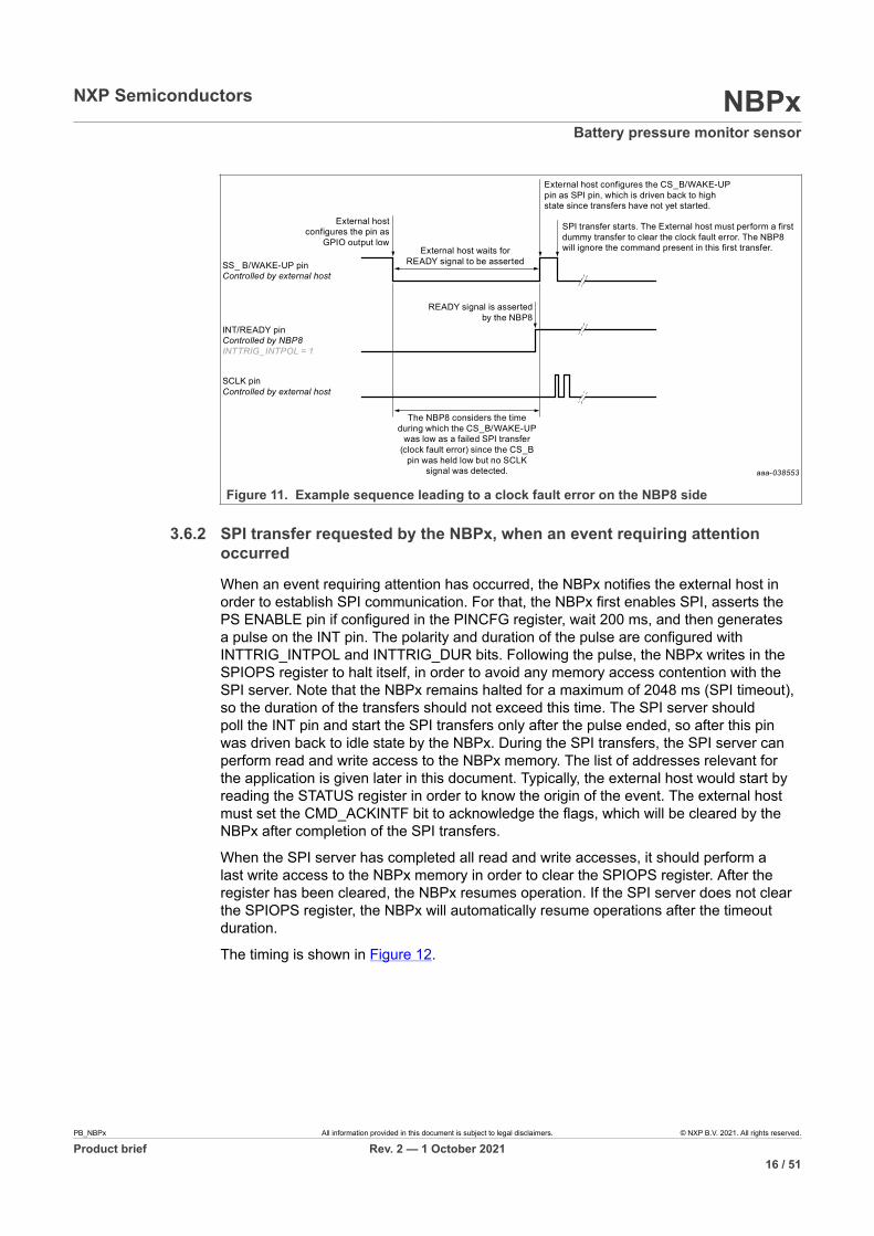
Important note: Figure 10 shows that the CS_B / WAKE-UP pin is held low by theexternal host from the moment the external host lowers the pin to request a transfer,until the end of the first SPI transfer. In reality, the actual sequence implemented by theexternal host may be different, taking into account the possible software implementationdescribed below.
To trigger the transfer request, the external host application may configure the CS_B /WAKE-UP pin as GPIO output low, and hold the pin in low state while polling the NBPxREADY pin. When the READY pin is asserted by the NBPx, this is an indication to theexternal host that the SPI transfers can start. To start the transfers, the external hostapplication may configure the CS_B / WAKE-UP as an SPI pin to be handled by theexternal host hardware SPI block. At that moment, the SPI transfers have not yet started,so the CS_B / WAKE-UP may be driven back to high state by the external host hardwareSPI block before being driven low again when the first transfer starts.
This implies that there may be a duration during which the CS_B / WAKE-UP pin isdriven to low state and then back to high state again, before the SPI transfers start,as illustrated in Figure 11 below. The NBPx logic considers this duration as a failedSPI transfer due to a clock fault error (CS_B pin lowered but no SCLK signal). Aftergenerating a clock fault error, the NBPx needs one 16-bit transfer to clear the error beforecontinuing normal operations. Consequently, the command inside the first 16-bit transferperformed by the external host will be ignored by the NBPx. The first transfer will beused by the NBPx to clear the clock fault error only. So, the external host has to considerthe first transfer to be a dummy transfer, during which the command is not taken intoaccount. It is only from the second transfer that the READ or WRITE commands will beprocessed by the NBPx.
PB_NBPx All information provided in this document is subject to legal disclaimers. © NXP B.V. 2021. All rights reserved.
Product brief Rev. 2 — 1 October 202115 / 51
NXP Semiconductors NBPxBattery pressure monitor sensor
aaa-038553
External hostconfigures the pin as
GPIO output low
READY signal is assertedby the NBP8
External host configures the CS_B/WAKE-UPpin as SPI pin, which is driven back to highstate since transfers have not yet started.
SPI transfer starts. The External host must perform a firstdummy transfer to clear the clock fault error. The NBP8will ignore the command present in this first transfer.External host waits for
READY signal to be asserted
The NBP8 considers the timeduring which the CS_B/WAKE-UP
was low as a failed SPI transfer(clock fault error) since the CS_B
pin was held low but no SCLKsignal was detected.
SS_ B/WAKE-UP pinControlled by external host
SCLK pinControlled by external host
INT/READY pinControlled by NBP8INTTRIG_INTPOL = 1
Figure 11. Example sequence leading to a clock fault error on the NBP8 side
3.6.2 SPI transfer requested by the NBPx, when an event requiring attentionoccurred
When an event requiring attention has occurred, the NBPx notifies the external host inorder to establish SPI communication. For that, the NBPx first enables SPI, asserts thePS ENABLE pin if configured in the PINCFG register, wait 200 ms, and then generatesa pulse on the INT pin. The polarity and duration of the pulse are configured withINTTRIG_INTPOL and INTTRIG_DUR bits. Following the pulse, the NBPx writes in theSPIOPS register to halt itself, in order to avoid any memory access contention with theSPI server. Note that the NBPx remains halted for a maximum of 2048 ms (SPI timeout),so the duration of the transfers should not exceed this time. The SPI server shouldpoll the INT pin and start the SPI transfers only after the pulse ended, so after this pinwas driven back to idle state by the NBPx. During the SPI transfers, the SPI server canperform read and write access to the NBPx memory. The list of addresses relevant forthe application is given later in this document. Typically, the external host would start byreading the STATUS register in order to know the origin of the event. The external hostmust set the CMD_ACKINTF bit to acknowledge the flags, which will be cleared by theNBPx after completion of the SPI transfers.
When the SPI server has completed all read and write accesses, it should perform alast write access to the NBPx memory in order to clear the SPIOPS register. After theregister has been cleared, the NBPx resumes operation. If the SPI server does not clearthe SPIOPS register, the NBPx will automatically resume operations after the timeoutduration.
The timing is shown in Figure 12.
PB_NBPx All information provided in this document is subject to legal disclaimers. © NXP B.V. 2021. All rights reserved.
Product brief Rev. 2 — 1 October 202116 / 51

NXP Semiconductors NBPxBattery pressure monitor sensor
Figure 12. SPI timing description when transfers are requested by the NBPx via the INTpin, with PINCFG_PTB1CFG = 5 and INTTRIG_INTPOL=1
3.7 Typical sequence timings
3.7.1 Periodic events
Figure 13 illustrates a sequence of periodic events. The sampling period configuredin the PSP register corresponds to the execution time of the sensor measurements,pressure change algorithm execution, and sleep duration. The available sampling periodsare achieved by adjusting the sleep time.
The execution time of the periodic ADC and Pcell Self-Test is not included in thesampling period.
aaa-037683
Sensorsmeas.
PressureChange
Algo
Sleep Sensorsmeas.
PressureChange
Algo
Sleep Sensorsmeas.
PressureChange
Algo
SleepPeriodicSelf-Test
(ADC and Pcell)
Lowpower
RUN
SAMPLING PERIOD SAMPLING PERIODSELF-TEST EXECUTION TIME + SAMPLINGPERIOD
STOP1 Lowpower
RUN STOP1 Lowpower
RUN STOP1RUN
Figure 13. Sequence of periodic events
3.7.2 NBPx notifying the external host
Figure 14 and Figure 15 illustrate a sequence of periodic events during which the NBPxnotifies the External host that an event requiring attention has occurred. When such anevent occurs, the NBPx generates a pulse on the INT pin and then waits until either theExternal host clears the SPIOPS register via SPI or the 2048 ms timeout period expires.
In the first example, the External host clears the SPIOPS during the last SPI transfer. TheNBPx then executes the commands that have been configured by the External host inthe CMD register.
The duration of the INT pulse is configured by the user with the INTTRIG_INTDURbit. The time during which the NBPx waits after generating the INT pulse depends onthe time needed by the External host to start the SPI transfers and the duration of the
PB_NBPx All information provided in this document is subject to legal disclaimers. © NXP B.V. 2021. All rights reserved.
Product brief Rev. 2 — 1 October 202117 / 51

NXP Semiconductors NBPxBattery pressure monitor sensor
SPI transfers, which itself depends on the SPI baud rate configured on the externalhost side and the number of transfers performed. The execution time of the commandsperformed by the NBPx is indicated at the end of this section. The duration of the Self-Test is indicated at the end of this section.
aaa-037684
Sensorsmeas.
PressureChange
Algo
Sleep Sensorsmeas.
PressureChange
Algo
Sleep Sensorsmeas.
PressureChange
Algo
Sleep
Lowpower
RUN
SAMPLING PERIOD SAMPLING PERIODDURATION CONTROLLED BY EXTERNAL HOST
This duration cannot exceed 2048 ms
STOP1 Lowpower
RUN STOP1 Lowpower
RUN STOP1
Enable SPIand
generateINT pulse
RUN
Wait whileSPIOPS is
not clear, ortimeoutoccurs
External host performsSPI transfers. The last
transfers clears SPIOPS
RUN
Commandsexecution
RUN
Figure 14. Sequence of events when NBPx notifies the external host of an event and theexternal host clears the SPIOPS register
The second example illustrates the sequence of events when the external host doesnot clear the SPIOPS register via SPI. In that case, the NBPx exits the waiting state ontimeout before entering the sleep state. Note that in this situation, the NBPx does notexecute the potential commands that could have been written in the CMD register. Thisis because exiting on timeout is not the expected sequence of events, indicating that aproblem occurred on the external host side.
aaa-037685
Sensorsmeas.
PressureChange
Algo
Sleep Sensorsmeas.
PressureChange
Algo
Sleep
Timeout occurs
Sensorsmeas.
PressureChange
Algo
Sleep
Lowpower
RUN
SAMPLING PERIOD SAMPLING PERIODTIMEOUT DURATION + SLEEP TIME
Duration = 2048 ms
STOP1 Lowpower
RUN STOP1 Lowpower
RUN STOP1
Enable SPIand
generateINT pulse
RUN
Wait while SPIOPS is notclear, or timeout occurs
RUN
Figure 15. Sequence of events when NBPx notifies the external host of an event but theexternal host does not clear the SPIOPS register
3.7.3 External host requesting an SPI transfer
Figure 16 and Figure 17 illustrate a sequence of periodic events during which theexternal host triggers an interrupt on the NBPx side via the WAKE-UP pin in order torequest SPI transfers.
If the WAKE-UP interrupt is triggered while the NBPx is in the sleep state (as in theabove example), the NBPx wakes up immediately, enables SPI, and raises the READYpin. That series of events (wake up, enable SPI and raise the READY pin) takes 125 µs.
If the WAKE-UP interrupt is triggered while the NBPx is performing sensormeasurements, Self-Test or any of the actions triggered by the CMD register, the NBPxfirst completes the ongoing action before enabling SPI and raising the READY pin.
In the first example, the external host clears the SPIOPS register during the last SPItransfer, as expected. Following the exit of the waiting state, the NBPx executes thecommands that have been configured by the external host in the CMD register beforecontinuing its sequence of events.
PB_NBPx All information provided in this document is subject to legal disclaimers. © NXP B.V. 2021. All rights reserved.
Product brief Rev. 2 — 1 October 202118 / 51

NXP Semiconductors NBPxBattery pressure monitor sensor
aaa-039747
Sensorsmeas.
PressureChange
Algo
Sleep Sensorsmeas.
PressureChange
Algo
Sleep Sensorsmeas.
PressureChange
Algo
Sleep
Lowpower
RUN
SAMPLING PERIOD SAMPLING PERIOD
DURATION CONTROLLED BY EXTERNAL HOST
This duration cannotexceed 2048 ms
STOP1 Lowpower
RUN STOP1 Lowpower
RUN STOP1
Wake up,enable SPIand raiseReady pin
RUN
Wait whileSPIOPS isnot clear, or
timeoutoccurs
External host performsSPI transfers. The last
transfers clears SPIOPS
WAKE-UP interrupt occurswhile the NBPx is in sleep
RUN
Commandsexecution
RUN
Figure 16. External host requests SPI transfers and then clears the SPIOPS register
In the second example, the external host does not clear the SPIOPS register during theSPI transfers, so the NBPx exits the waiting state on timeout before entering the sleepstate. Note that in this situation, the NBPx does not execute the potential commands thatcould have been written in the CMD register. This is because exiting on timeout is not theexpected sequence of events, indicating that a problem occurred on the external hostside.
aaa-039748
Sensorsmeas.
PressureChange
Algo
Sleep Sensorsmeas.
PressureChange
Algo
Sleep Sensorsmeas.
PressureChange
Algo
Sleep
Lowpower
RUN
SAMPLING PERIOD SAMPLING PERIOD
STOP1 Lowpower
RUN STOP1
Sleep
STOP1 Lowpower
RUN STOP1
WAKE-UP interrupt occurswhile the NBPx is in sleep
Wake up,enable SPIand raise
READY pin
RUN
Wait while SPIOPS is notclear, or timeout occurs
RUN
Timeout occurs
SAMPLING PERIOD + PORTION OF SLEEP + TIMEOUT DURATION
Duration = 2048 ms
Figure 17. External host requests SPI transfers but does not clear the SPIOPS register
3.7.4 Summary of execution times
Table 3 summarizes the execution times of the different actions. Sensor measurementsinclude raw pressure, raw temperature and raw voltage readings, followed by pressure,temperature, and voltage compensations.
Action Periodic/Triggered Duration
Sensor measurements Periodic 4 ms
Pressure change algorithm Periodic 100 μs
ADC and Pcell self-test Periodic 3.47 ms
ADC self-test Triggered by CMD_ADCST 455 µs
Pcell self-test Triggered by CMD_PST 3.32 ms
Firmware verification Triggered by CMD_FV 132 ms
Reset registers Triggered by CMD_RESET 206 µs
Clear FIFO Triggered by CMD_CLRFIFO 185 µs
Acknowledge INTF Triggered by CMD_ACKINTF 18 µs
Table 3. Summary of execution times
PB_NBPx All information provided in this document is subject to legal disclaimers. © NXP B.V. 2021. All rights reserved.
Product brief Rev. 2 — 1 October 202119 / 51

NXP Semiconductors NBPxBattery pressure monitor sensor
3.8 Read/write registers accessible by the external host over SPISection 3.8 details the addresses of the NBPx accessible over SPI by the external host.
Address Name Bit 7 Bit 6 Bit 5 Bit 4 Bit 3 Bit 2 Bit 1 Bit 0
$0038 SPIOPS reserved reserved reserved reserved reserved CORE_TR_HOLD
reserved reserved
$0050 PSP PSP[7:0]
$0051 STPER STPER[7:0]
$0052 PINCFG reserved reserved reserved reserved reserved PINCFG[2:0]
$0053 INTTRIG reserved reserved INTPOL INTDUR FVERR STERR SENSERR SENSRDY
$0054 PCCFG reserved reserved reserved reserved reserved STEN RTEN FTEN
$0055 STATUS INTF PCSTF PCRTF PCFTF FVF PSTF ADCSTF SENSF
$0056 SENSTATUS ADCERR LVW POVER PUNDER TOVER TUNDER VOVER VUNDER
$0057 CMD ACKINTF reserved reserved CLRFIFO RESET FV PST ADCST
$0058 PCDEBT PCDEBT[7:0]
$0059 PCFIXTH PCFIXT[15:8]
$005A PCFIXTL PCFIXT[7:0]
$005B PCMINT PCMINT[7:0]
$005C PCRELTH PCRELT[15:8]
$005D PCRELTL PCRELT[7:0]
$005E PCSLOPETH PCSLOPET[15:8]
$005F PCSLOPETL PCSLOPET[7:0]
$0070: TCODE TCODE[7:0]
$0071 VCODE VCODE[7:0]
$0075 INDFIFO INDFIFO[7:0]
$0076to
$008D
PFIFOH1[15:8]
PFIFOL1[7:0]to
PFIFOH12[15:8]PFIFOL12[7:0]
PFIFO1[15:0] through PFIFO12[15:0]
Table 4. Read and write addresses summary
The detail of the read/write targets is given below.
Bit 7 6 5 4 3 2 1 0
R/W Bit7 Bit6 Bit5 Bit4 Bit3 CORE_TR_
HOLD
Bit1 Bit0
POR or User Reset ($0) 0 0 0 0 0 0 0 0
Table 5. SPI Operations (SPIOPS) (address 0x0038)
PB_NBPx All information provided in this document is subject to legal disclaimers. © NXP B.V. 2021. All rights reserved.
Product brief Rev. 2 — 1 October 202120 / 51

NXP Semiconductors NBPxBattery pressure monitor sensor
Fields Description
Reserved[7:3]SPIOPS[2]
Reserved[1:0]
SPIOPS[2] CORE_TR_HOLD - Core read/write accesses on hold. This bit is used to ensure that SPIbecomes the only internal bus server with unhindered access to the system registers.0 = internal bus normal; SPI is granted access only if the internal CPU is not accessing the same sub-bus modules; Result of Reset.1 = internal CPU on hold; SPI has unhindered access to the system registers, for the external hostSPI server to read or write as needed. Must be cleared to 0 at the end of the external host SPI servertransaction, to release the internal CPU.
Table 6. SPIOPS fields description
Bit 7 6 5 4 3 2 1 0
R/W Bit7 Bit6 Bit5 Bit4 Bit3 Bit2 Bit1 Bit0
POR or User Reset ($4) 0 0 0 0 0 1 0 0
Table 7. Pressure Sampling Period (PSP) (address 0x0050)
Fields Description
7-0PSP[7:0]
The PSP[7:0] configures the period at which pressure measurement is triggered. The operating range ofPSP[7:0] is $00 to $06, resulting in the following sampling periods:PSP[7:0] = $00: SAMPLING PERIOD = 10 msPSP[7:0] = $01: SAMPLING PERIOD = 20 msPSP[7:0] = $02: SAMPLING PERIOD = 40 msPSP[7:0] = $03: SAMPLING PERIOD = 70 msPSP[7:0] = $04: SAMPLING PERIOD = 135 msPSP[7:0] = $05: SAMPLING PERIOD = 510 msPSP[7:0] = $06: SAMPLING PERIOD = 1000 msPSP[7:0] = $07 to $FF = same as $06.The typical sampling periods may vary due to the LFO clock tolerance listed in Section 8 "Electricalspecifications".The reset value is $04, resulting in a 135 ms period. When the PSP value is changed by the ExternalHost, the Pressure FIFO is cleared after completion of the SPI transfers
Table 8. PSP fields description
Bit 7 6 5 4 3 2 1 0
R/W Bit7 Bit6 Bit5 Bit4 Bit3 Bit2 Bit1 Bit0
POR or User Reset ($FF) 1 1 1 1 1 1 1 1
Table 9. Self-Test Execution Period (STPER) (address 0x0051)
PB_NBPx All information provided in this document is subject to legal disclaimers. © NXP B.V. 2021. All rights reserved.
Product brief Rev. 2 — 1 October 202121 / 51

NXP Semiconductors NBPxBattery pressure monitor sensor
Fields Description
7-0STPER[7:0]
The STPER[7:0] configures the period at which ADC and Pcell Self-Test is performed. The operatingrange of STPER[7:0] is $00 to $FF. A value of $00 disables the periodic Self-Test. Any other value givesa range of Self-Test execution period from 1 to 255 x SAMPLING PERIOD. Depending on the value ofthe bits for the PSP[7:0], the Self-Test execution period can nominally be from 2.55 s to 255 s.The conversion from the decimal value of STPER[7:0] to the period in milliseconds is given as describedby the following equation.SELF TEST PERIOD = STPER[7:0] * SAMPLING PERIOD
Table 10. STPER fields description
Bit 7 6 5 4 3 2 1 0
R/W — — — — — PINCFG2 PINCFG1 PINCFG0
POR or User Reset ($00) 0 0 0 0 0 0 0 0
Table 11. PIN Configuration (PINCFG) (address 0x0052)
Fields Description
7–3Reserved
Reserved bits—not for user access
2-0PINCFG[2:0]
The PINCFG[2:0] configures the PTB1 pin function as described below:PINCFG[2:0] = 0 0 0: the pin is disabledPINCFG[2:0] = 0 0 1: the pin is disabledPINCFG[2:0] = 0 1 0: the pin is disabledPINCFG[2:0] = 0 1 1: the pin is disabledPINCFG[2:0] = 1 0 0: the PS ENABLE function is enabled and the pin is idle at logic 1, asserted at logic0PINCFG[2:0] = 1 0 1: the PS ENABLE function is enabled and the pin is idle at logic 0, asserted at logic1PINCFG[2:0] = 1 1 0: the pin is disabledPINCFG[2:0] = 1 1 1: the pin is disabled
Table 12. PINCFG fields description
Bit 7 6 5 4 3 2 1 0
R/W — — INTPOL INTDUR FVERR STERR SENSERR SENSRDY
POR or UserReset ($3E)
— — 1 1 1 1 1 0
Table 13. Interrupt pulse Trigger (INTTRIG) (address 0x0053)
Fields Description
7:6 Reserved Reserved bits—not for user access
Table 14. INTTRIG fields description
PB_NBPx All information provided in this document is subject to legal disclaimers. © NXP B.V. 2021. All rights reserved.
Product brief Rev. 2 — 1 October 202122 / 51

NXP Semiconductors NBPxBattery pressure monitor sensor
Fields Description
5INTPOL
INT pin Polarity – Selects the polarity of the INT/READY pin.0 The pin is asserted to logic 0 during the pulse, and idle at logic 11 The pin is asserted to logic 1 during the pulse, and idle at logic 0
4INTDUR
INT pulse Duration - Selects the duration of the pulse generated by the NBPx on the INT pin.0 Pulse on the INT pin has a duration of 4 ms1 Pulse on the INT pin has a duration of 8 ms
3FVERR
Firmware Verification Error – Selects whether the NBPx generates a pulse on the INT pin when theFirmware Verification execution completes with errors.0 No pulse generated on the INT pin when the Firmware Verification execution completes with errors1 Pulse generated on the INT pin when the Firmware Verification execution completes with errors
2STERR
Self-Test Error – Selects whether the NBPx generates a pulse on the INT pin when the Pcell or ADCSelf-Test execution completes with errors.0 No pulse generated on the INT pin when the Self-Test execution completes with errors1 Pulse generated on the INT pin when the Self-Test execution completes with errors
1SENSERR
Sensor Error – Selects whether the NBPx generates a pulse on the INT pin when the sensor dataacquisition completed with errors.0 No pulse generated on the INT pin when the sensor data acquisition completed with errors1 Pulse generated on the INT pin when the sensor data acquisition completed with errors
0SENSRDY
Sensor Data Ready – Selects whether the NBPx generates a pulse on the INT pin when the sensor dataacquisition completed, and new sensor data is available.0 No pulse generated on the INT pin when the sensor data acquisition completed, and new sensor datais available1 Pulse generated on the INT pin when the sensor data acquisition completed, and sensor data isavailable
Table 14. INTTRIG fields description...continued
Bit 7 6 5 4 3 2 1 0
R -- -- -- -- -- STEN RTEN FTEN
POR or UserReset ($01)
0 0 0 0 0 0 0 1
Table 15. Pressure Change Configuration (PCCFG) (address $0054)
Fields Description
7-3Reserved
Reserved bits – Not for user access.
2STEN
Slope Threshold Enable – Enables the option to monitor the pressure change of rate vs. a change ofrate threshold.0 Option disabled1 Option enabled
1RTEN
Relative Threshold Enable – Enables the option to monitor the pressure vs. a relative threshold.0 Option disabled1 Option enabled
Table 16. PCCFG fields description
PB_NBPx All information provided in this document is subject to legal disclaimers. © NXP B.V. 2021. All rights reserved.
Product brief Rev. 2 — 1 October 202123 / 51

NXP Semiconductors NBPxBattery pressure monitor sensor
Fields Description
0FTEN
Fixed Threshold Enable – Enables the option to monitor the pressure vs. a fixed threshold.0 Option disabled1 Option enabled
Table 16. PCCFG fields description...continued
Bit 7 6 5 4 3 2 1 0
R INTF PCSTF PCRTF PCFTF FVF PSTF ADCSTF SENSF
POR or UserReset ($00)
0 0 0 0 0 0 0 0
Table 17. Status of the latest executions (STATUS) (address 0x0055)
Fields Description
7INTF
INT pin Flag – Indicates whether a condition for pulse generation is met, and a pulse on the INT pin isgenerated.0 No pulse on the INT pin is generated1 Pulse on the INT pin is generated. Events that occurred are detailed in bits 6:0. Including INTF, eachof the bits are cleared after completion of the SPI transfers, if CMD_ACKF was set by the external host
6PCSTF
Pressure Change Slope Threshold Flag – Indicates whether the pressure rate of change has exceededthe rate of change threshold PCSLOPET.0 Condition is not met, the pressure rate of change has not exceeded the threshold1 Condition is met, the pressure rate of change has exceeded the threshold. STATUS_INTF is set and apulse is generated on the INT pin.
5PCRTF
Pressure Change Relative Threshold Flag – Indicates whether the pressure has exceeded the relativethreshold PCRELT.0 Condition is not met, the pressure has not exceeded the threshold1 Condition is met, the pressure has exceeded the threshold. STATUS_INTF is set and a pulse isgenerated on the INT pin.
4PCFTF
Pressure Change Fixed Threshold Flag – Indicates whether the pressure has exceeded the fixedthreshold PCFIXT.0 Condition is not met, the pressure has not exceeded the threshold1 Condition is met, the pressure has exceeded the threshold. STATUS_INTF is set and a pulse isgenerated on the INT pin.
3FVF
Firmware Verification Flag– Indicates the status of the latest firmware verification.0 The latest firmware verification completed with no errors1 The latest firmware verification completed with errors. If INTTRIG_FVERR is set, STATUS_INTF is setand a pulse is generated on the INT pin.
2PSTF
Pcell Self-Test Flag – Indicates the status of the latest Pcell Self-Test.0 The latest Pcell Self-Test completed with no errors1 The latest Pcell Self-Test completed with errors. If INTTRIG_STERR is set, STATUS_INTF is set anda pulse is generated on the INT pin.
1ADCSTF
ADC Self-Test Flag – Indicates the status of the latest ADC Self-Test.0 The latest ADC Self-Test completed with no errors1 The latest ADC Self-Test completed with errors. If INTTRIG_STERR is set, STATUS_INTF is set and apulse is generated on the INT pin.
Table 18. STATUS fields description
PB_NBPx All information provided in this document is subject to legal disclaimers. © NXP B.V. 2021. All rights reserved.
Product brief Rev. 2 — 1 October 202124 / 51

NXP Semiconductors NBPxBattery pressure monitor sensor
Fields Description
0SENSF
Sensor Flag – Indicates the status of the latest sensor acquisition.0 The latest sensor acquisition completed with no errors, the SENSTATUS fields are all clear. IfINTTRIG_SENSRDY is set, a pulse is generated on the INT pin after completion of the acquisition1 The latest sensor acquisition completed with errors detailed in the SENSTATUS fields. If INTTRIG_SENSERR or INTTRIG_SENSRDY is set, INTF is set and a pulse is generated on the INT pin aftercompletion of the acquisition.
Table 18. STATUS fields description...continued
Bit 7 6 5 4 3 2 1 0
R ADCERR LVW POVER PUNDER TOVER TUNDER VOVER VUNDER
POR or UserReset ($00)
0 0 0 0 0 0 0 0
Table 19. Sensor Status (SENSTATUS) (address 0x0056)
Fields Description
7ADCERR
ADC Error – Indicates whether an ADC error occurred during the latest sensor acquisition.0 No ADC error occurred during the latest sensor acquisition1 An ADC error occurred during the latest sensor acquisition. The bit is cleared after completion of theSPI transfers, if CMD_ACKF was set by the external host
6LVW
Low Voltage Warning – Indicates whether the voltage is suspected to be below operating range forpressure measurement.0 Voltage is in-range1 Voltage is suspected to be below operating range, pressure accuracy is not guaranteed. The bit iscleared after completion of the SPI transfers, if CMD_ACKF was set by the external host
5POVER
Pressure Overflow – Indicates whether the latest pressure acquisition resulted in an overflow.0 The latest pressure measurement did not overflow1 The latest pressure measurement resulted in an overflow. The bit is cleared after completion of theSPI transfers, if CMD_ACKF was set by the external host
4PUNDER
Pressure Underflow – Indicates whether the latest pressure acquisition resulted in an underflow.0 The latest pressure measurement did not underflow1 The latest pressure measurement resulted in an underflow. The bit is cleared after completion of theSPI transfers, if CMD_ACKF was set by the external host
3TOVER
Temperature Overflow – Indicates whether the latest temperature acquisition resulted in an overflow.0 The latest temperature measurement did not overflow1 The latest temperature measurement resulted in an overflow. The bit is cleared after completion of theSPI transfers, if CMD_ACKF was set by the external host
2TUNDER
Temperature Underflow – Indicates whether the latest temperature acquisition resulted in an underflow.0 The latest temperature measurement did not underflow1 The latest temperature measurement resulted in an underflow. The bit is cleared after completion ofthe SPI transfers, if CMD_ACKF was set by the external host
1VOVER
Voltage Overflow – Indicates whether the latest voltage acquisition resulted in an overflow.0 The latest voltage measurement did not overflow1 The latest voltage measurement resulted in an overflow. The bit is cleared after completion of the SPItransfers, if CMD_ACKF was set by the external host
Table 20. SENSTATUS fields description
PB_NBPx All information provided in this document is subject to legal disclaimers. © NXP B.V. 2021. All rights reserved.
Product brief Rev. 2 — 1 October 202125 / 51

NXP Semiconductors NBPxBattery pressure monitor sensor
Fields Description
0VUNDER
Voltage Underflow – Indicates whether the latest voltage acquisition resulted in an underflow.0 The latest voltage measurement did not underflow1 The latest voltage measurement resulted in an underflow. The bit is cleared after completion of theSPI transfers, if CMD_ACKF was set by the external host
Table 20. SENSTATUS fields description...continued
Bit 7 6 5 4 3 2 1 0
R/W ACKINTF -- -- CLRFIFO RESET FV PST ADCST
POR or UserReset ($00)
0 0 0 0 0 0 0 0
Table 21. Command (CMD) (address 0x0057)
Fields Description
7ACKINTF
Acknowledge INT Flag – If the external host writes logic 1 to this bit, the STATUS, and SENSTATUSregisters will be cleared after completion of the SPI transfers.0 No effect1 Clearing the STATUS, and SENSTATUS registers is requested. The NBPx clears this bit aftercompletion of the command
6:5Reserved
Reserved bits – Not for user access.
4CLRFIFO
Clear FIFO - If the external host writes logic 1 to this bit, the Pressure FIFO will be cleared aftercompletion of the SPI transfers.0 No effect1 Clearing the Pressure FIFO is requested. The NBPx clears this bit after completion of the command
3RESET
Reset – Indicates to the NBPx whether a one-time register reset is requested after completion of the on-going SPI transfer sequence. Register reset sets all read/write user targets to their reset values.0 No register reset requested1 Register reset is requested. The NBPx clears this bit after completion of the command
2FV
Firmware Verification – Indicates to the NBPx whether a one-time Firmware Verification is requestedafter completion of the on-going SPI transfer sequence.0 No Firmware Verification requested1 Firmware Verification requested. The NBPx clears this bit after completion of the command
1PST
Pressure cell Self-Test – Indicates to the NBPx whether a one-time pressure cell Self-Test is requestedafter completion of the on-going SPI transfer sequence.0 No pressure cell Self-Test requested1 Pressure cell Self-Test requested. The NBPx clears this bit after completion of the command
0ADCST
ADC Self-Test – Indicates to the NBPx whether a one-time ADC Self-Test is requested after completionof the on-going SPI transfer sequence.0 No ADC Self-Test requested1 ADC Self-Test requested. The NBPx clears this bit after completion of the command
Table 22. CMD fields description
PB_NBPx All information provided in this document is subject to legal disclaimers. © NXP B.V. 2021. All rights reserved.
Product brief Rev. 2 — 1 October 202126 / 51

NXP Semiconductors NBPxBattery pressure monitor sensor
Bit 7 6 5 4 3 2 1 0
R/W Bit7 Bit6 Bit5 Bit4 Bit3 Bit2 Bit1 Bit0
POR or UserReset ($05)
0 0 0 0 0 1 0 1
Table 23. Pressure Change Debounce Threshold (PCDEBT) (address 0x0058)
Fields Description
7-0PCDEBT[7:0]
The PCDEBT[7:0] debounce threshold defines the minimum debounce value to consider that a PressureChange condition has been met. The operating range of PCDEBT[7:0] is 0 to 254. If this register isconfigured to value 255 by the External host during an SPI transfer, the value will be changed to 254 aftercompletion of the SPI transfers.
Table 24. PCDEBT fields description
Bit 7 6 5 4 3 2 1 0
R/W Bit15 Bit14 Bit13 Bit12 Bit11 Bit10 Bit9 Bit8
POR or UserReset ($03)
0 0 0 0 0 0 1 1
Table 25. Pressure Change Fixed Threshold High (PCFIXTH) (address 0x0059)
Bit 7 6 5 4 3 2 1 0
R/W Bit7 Bit6 Bit5 Bit4 Bit3 Bit2 Bit1 Bit0
POR or UserReset ($20)
0 0 1 0 0 0 0 0
Table 26. Pressure Change Fixed Threshold Low (PCFIXTL) (address 0x005A)
Fields Description
15-0PCFIXT[15:0]
The two PCFIXT[15:0] define the fixed threshold value used in the Fixed Threshold algorithm. WhenPCCFG_FTEN is set, the flag STATUS_PCFTF is raised when pressure is consistently above thisthreshold.
Table 27. PCFIXTH/L fields description
Bit 7 6 5 4 3 2 1 0
R/W Bit7 Bit6 Bit5 Bit4 Bit3 Bit2 Bit1 Bit0
POR or UserReset ($03)
0 0 0 0 0 0 1 1
Table 28. Pressure Change Minimum Threshold (PCMINT) (address $005B)
PB_NBPx All information provided in this document is subject to legal disclaimers. © NXP B.V. 2021. All rights reserved.
Product brief Rev. 2 — 1 October 202127 / 51

NXP Semiconductors NBPxBattery pressure monitor sensor
Fields Description
7-0PCMINT[7:0]
The PCMINT[7:0] defines the minimum number of counts by which the current pressure value must exceedthe previous pressure value, for the NBPx program to consider that the pressure is increasing.
Table 29. PCMINT fields description
Bit 7 6 5 4 3 2 1 0
R/W Bit15 Bit14 Bit13 Bit12 Bit11 Bit10 Bit9 Bit8
POR or UserReset ($00)
0 0 0 0 0 0 0 0
Table 30. Pressure Change Relative Threshold High (PCRELTH) (address $005C)
Bit 7 6 5 4 3 2 1 0
R/W Bit7 Bit6 Bit5 Bit4 Bit3 Bit2 Bit1 Bit0
POR or UserReset ($32)
0 0 1 1 0 0 1 0
Table 31. Pressure Change Relative Threshold Low (PCRELTL) (address $005D)
Fields Description
15-0PCRELT[15:0]
The two PCRELT[15:0] define the relative threshold value used in the Relative Threshold algorithm. WhenPCCFG_RTEN is set, the flag STATUS_PCRTF is raised when pressure increase is consistently abovethis threshold.
Table 32. PCRELTH/L fields description
Bit 7 6 5 4 3 2 1 0
R/W Bit15 Bit14 Bit13 Bit12 Bit11 Bit10 Bit9 Bit8
POR or UserReset ($00)
0 0 0 0 0 0 0 0
Table 33. Pressure Change Slope Threshold High (PCSLOPETH) (address 0x005E)
Bit 7 6 5 4 3 2 1 0
R/W Bit7 Bit6 Bit5 Bit4 Bit3 Bit2 Bit1 Bit0
POR or UserReset ($40)
0 1 0 0 0 0 0 0
Table 34. Pressure Change Slope Threshold Low (PCSLOPETL) (address 0x005F)
PB_NBPx All information provided in this document is subject to legal disclaimers. © NXP B.V. 2021. All rights reserved.
Product brief Rev. 2 — 1 October 202128 / 51

NXP Semiconductors NBPxBattery pressure monitor sensor
Fields Description
15-0PCSLOPET[15:0]
The two PCSLOPET[15:0] define the rate of change threshold value used in the Slope Thresholdalgorithm. When PCCFG_STEN is set, the flag STATUS_PCSTF is raised when the pressure rateof change exceeds this threshold. The slope is calculated by ΔP * 128 / number sampling periodswhere: –ΔP is the pressure increase, in counts–128 is a multiplication coefficient, to scale the slope–number sampling periods is the number of sampling periods during which the pressure has beenincreasing until the slope is calculated Note that the slope value is expressed in pressure counts per sampling period. The conversion tokPa/s depends on the pressure sensitivity and the user-selected sampling period value.Example:For a pressure sensitivity equal to 0.2kPa/LSB and a sampling period selected as 135 ms, apressure increase of 10 kPa over 1 second corresponds to a pressure increase of 50 pressurecounts over 7.4 sampling periods, resulting in a slope value of 50*128/7.4 = 864. If the sampling period is selected as 70 ms, then a pressure increase of 10 kPa over 1 secondcorresponds to a pressure increase of 50 pressure counts over 14.3 sampling periods, resulting in aslope value of 50*128/14.3 = 447.
Table 35. PCSLOPETH/L fields description
Bit 7 6 5 4 3 2 1 0
R Bit7 Bit6 Bit5 Bit4 Bit3 Bit2 Bit1 Bit0
POR or UserReset ($70)
0 0 0 0 0 0 0 0
Table 36. Temperature measurement (TCODE) (address $0070)
Fields Description
7-0TCODE[7:0]
The TCODE[7:0] stores the most recent compensated internal device temperature measurement, andcan be converted to degC by the transfer function T °C = (1 °C / LSB × TCODE) – 55 °C
Table 37. TCODE fields description
Bit 7 6 5 4 3 2 1 0
R Bit7 Bit6 Bit5 Bit4 Bit3 Bit2 Bit1 Bit0
POR or UserReset ($70)
0 0 0 0 0 0 0 0
Table 38. Voltage measurement (VCODE) (address $0071)
PB_NBPx All information provided in this document is subject to legal disclaimers. © NXP B.V. 2021. All rights reserved.
Product brief Rev. 2 — 1 October 202129 / 51

NXP Semiconductors NBPxBattery pressure monitor sensor
Fields Description
7-0VOCODE[7:0]
The VCODE[7:0] stores the most recent compensated internal device voltage measurement, and can beconverted to V by the transfer function V = (0.01 V / LSB × VCODE) + 1.22 V.
Table 39. Voltage measurement fields description
Bit 7 6 5 4 3 2 1 0
R Bit7 Bit6 Bit5 Bit4 Bit3 Bit2 Bit1 Bit0
POR or UserReset ($76)
0 1 1 1 0 1 1 0
Table 40. Index of the pressure FIFO (INDFIFO) (address $0075)
Fields Description
7-0INDFIFO[7:0]
The INDFIFO[7:0] stores the address of the last byte written in the pressure PFIFO.
Table 41. INDFIFO fields description
Bit 7 6 5 4 3 2 1 0
R Bit15 Bit14 Bit13 Bit12 Bit11 Bit10 Bit9 Bit8
R Bit7 Bit6 Bit5 Bit4 Bit3 Bit2 Bit1 Bit0
POR or UserReset ($00)
0 0 0 0 0 0 0 0
Table 42. Pressure FIFO (PFIFOH/Lx) (addresses $0076 - $008D)
Fields Description
15:8PFIFOHx[15:8]
7:0PFIFOLx[7:0][1]
The PFIFO stores the 12 latest pressure measurements. The PFIFO is implemented as a rolling buffer:the most recent pressure measurement overwrites the oldest one. The INDFIFO index holds the valueof the last address written. Each entry shall occupy two bytes, high byte at first address and low byte atsecond address, for a total of 24 bytes.
Table 43. PFIFOH/Lx fields description
[1] Where x = 1 to 12.
4 Applications
• Power-train for traction (EV) battery systems• Renewable energy storage: Portable energy storage containers, energy field arrays• Fast thermal runaway detection for lithium-ion cells• Battery management system• Lithium-ion battery pack: State of health
PB_NBPx All information provided in this document is subject to legal disclaimers. © NXP B.V. 2021. All rights reserved.
Product brief Rev. 2 — 1 October 202130 / 51

NXP Semiconductors NBPxBattery pressure monitor sensor
5 Ordering information
Part Number Pressure Range Pressure tolerances
NBPxFD4T1 40 kPa to 250 kPa Standard tolerances
Table 44. Ordering options
NBPxFD4T1
where
x = "8" or "9" (SPI or SPI/PWM output
NBPx product code definition
6 Block diagram
Figure 18 presents the device's main blocks and their signal interactions. Powermanagement controls and bus control signals are not shown in this block diagram forclarity.
PB_NBPx All information provided in this document is subject to legal disclaimers. © NXP B.V. 2021. All rights reserved.
Product brief Rev. 2 — 1 October 202131 / 51

NXP Semiconductors NBPxBattery pressure monitor sensor
aaa-037679
BDMController
S088b CPU
InterruptController
PadMUX
GPIOIRQ
BKGDSPITPMADCetc.
Pwr. ModeController
ResetCntl. Mod.
NV RAM64 x 8
Sys RAM512 x 8
FlashController
Flash NVM16k x 8
SystemInt. Mod.
PTA0 - 4PTB0 - 1
SPI
M0
BusArb.MUX
S0
S1
S2
S3M1
KeyBdInterrupt
Int. ClksSys
COPTimer
PWU/RTITimer
Peripheral Bus
FreeRun Cntr.
Gain Offsetand Coeff.
Gain Offsetamps
P-cellRef.
SARADC
Bandgap
Temp Sensor
SMI
Buffer LPF
2chTPM
OffsetDAC
CtoVConverter
CtoVMUX
AtoDMUXP-cell
Sns.
Figure 18. Block diagram
7 Pinning information
This section describes the pin layout and general function of each pin.
PB_NBPx All information provided in this document is subject to legal disclaimers. © NXP B.V. 2021. All rights reserved.
Product brief Rev. 2 — 1 October 202132 / 51

NXP Semiconductors NBPxBattery pressure monitor sensor
7.1 PinningThe device pinout is shown in Figure 19 for the orientation of the pressure port up.
aaa-037680
CGND18
17
16
15
14
13
CGND
PTA1
PTA2
PTA3
PTB0
PTA
47 8 9 10 11 12
RST
B
VD
DA
GN
D
VD
D
n.c.
n.c.
24 23 22 21 20 19
n.c.
PTB1
n.c.
CG
ND
PTA
0
n.c.
Pin 1index area
Transparent top view
1
2
3
4
5
6
n.c.
n.c.
n.c.
n.c.
n.c.
Note: Pins 1-6 are mechanically and electrically connected to the central flag; See Section 11 fordetails. If additional ground is desired, any of the pins 1-6 may be routed to circuit board groundplane, or the central flag may be connected to circuit board ground plane with vias.
Figure 19. Pin configuration
7.2 Pin description
Symbol Pin Function Description
n.c. 1 — Do not connect electrical signals to this pin; solder joint only.
n.c. 2 — Do not connect electrical signals to this pin; solder joint only.
n.c. 3 — Do not connect electrical signals to this pin; solder joint only.
n.c. 4 — Do not connect electrical signals to this pin; solder joint only.
n.c. 5 — Do not connect electrical signals to this pin; solder joint only.
n.c. 6 — Do not connect electrical signals to this pin; solder joint only.
PTA4 7 PTA4 / BKGD PTA4 Pin - The PTA4 pin places the device in the BACKGROUND DEBUGmode (BDM) to evaluate CPU code and transfer data to/from the internalmemory. If the BKGD/PTA4 pin is held low when the device comes out of apower-on-reset (POR), the device switches into the ACTIVE BACKGROUNDDEBUG mode (BDM).The BKGD/PTA4 pin has an internal pullup device or can be connected toVDD in the application, unless there is a need to enter BDM operation afterthe device as been soldered into the PWB. If in-circuit BDM is desired, theBKGD/PTA4 pin should be connected to VDD through a resistor (~10 kΩor greater) which can be over-driven by an external signal. This resistorreduces the possibility of inadvertently activating the debug mode in theapplication due to an EMC event.When the application programs port A to GPIOs, PTA4 becomes output-only.
Table 45. Pin description
PB_NBPx All information provided in this document is subject to legal disclaimers. © NXP B.V. 2021. All rights reserved.
Product brief Rev. 2 — 1 October 202133 / 51

NXP Semiconductors NBPxBattery pressure monitor sensor
Symbol Pin Function Description
RST_B 8 Reset / VPPprogramming voltage
The RST_B pin is used for test and establishing the BDM condition andproviding the programming voltage source to the internal FLASH memory.This pin can also be used to direct to the CPU to the reset vector.The RST_B pin has an internal pullup device and can be connected to VDDin the application unless there is a need to enter BDM operation after thedevice as been soldered to the PWB. If in-circuit BDM is desired, the RST_Bpin can be left unconnected; but should be connected to VDD through a lowimpedance resistor (<10 kΩ) which can be over-driven by an external signal.This low impedance resistor reduces the possibility of getting into the debugmode in the application due to an EMC event.Activation of the external reset function occurs when the voltage on theRST_B pin goes below 0.3 × VDD for at least 100 ns before rising above0.7 × VDD.
VDDA 9 Analog supply The analog circuits operate from a single power supply connected to the unitthrough the VDDA pin. VDDA is the positive supply and GND is the ground.The conductors to the power supply should be connected to the VDDA andGND pins and locally decoupled.Care should be taken to reduce measurement signal noise by separatingthe VDD, GND, VDDA, and RFGND pins using a “star” connection suchthat each metal trace does not share any load currents with other externaldevices.
GND 10 Digital and analogground
The digital circuits operate from a single power supply connected to the unitthrough the VDD and GND pins. GND is the ground. Care should be taken toreduce measurement signal noise by separating the GND and RFGND pinsusing a “star” connection such that each metal trace does not share any loadcurrents with other external devices.
VDD 11 Digital supply The digital circuits operate from a single power supply connected to the unitthrough the VDD and GND pins. VDD is the positive supply. The conductorsto the power supply should be connected to the VDD and GND pins andlocally decoupled.
n.c. 12 — Do not connect electrical signals to this pin; solder joint only.
PTB0 13 PTB0 / TPMCH0 /AD3
The PTB[0] pin is a general-purpose I/O pin. This pin can be configuredas a nominal bidirectional I/O pin with programmable pullup devices. Usersoftware must configure the general-purpose I/O pin (PTB[1:0]) so that theydo not result in “floating” inputs. PTB0 can be mapped to TPM channel 0, orto ADC channel 3.
PTA3 14 PTA3 / KBI3 / SOCI The PTA[3] pin is a general-purpose I/O pin. The pulldown devices can onlybe activated if the wake-up interrupt capability is enabled. User softwaremust configure the general-purpose I/O pins so that they do not result in“floating” inputs. PTA[3] maps to keyboard interrupt function bit [3]. When SPIis enabled, PTA[3] serves as SOCI.
PTA2 15 PTA2 / KBI2 / SICO The PTA[2] pin is a general-purpose I/O pin. The pulldown devices can onlybe activated if the wake-up interrupt capability is enabled. User softwaremust configure the general-purpose I/O pins so that they do not result in“floating” inputs. PTA[2] maps to keyboard interrupt function bit [2]. When SPIis enabled, PTA[2] serves as SICO.
PTA1 16 PTA1 / KBI1 / SCLK The PTA[1] pin is a general-purpose I/O pin. The pulldown devices can onlybe activated if the wake-up interrupt capability is enabled. User softwaremust configure the general-purpose I/O pins so that they do not result in“floating” inputs. PTA[1] maps to keyboard interrupt function bit [1]. When SPIis enabled, PTA[1] serves as SCLK
Table 45. Pin description...continued
PB_NBPx All information provided in this document is subject to legal disclaimers. © NXP B.V. 2021. All rights reserved.
Product brief Rev. 2 — 1 October 202134 / 51

NXP Semiconductors NBPxBattery pressure monitor sensor
Symbol Pin Function Description
CGND 17 — To be connected to ground by the application.
CGND 18 — To be connected to ground by the application.
PTA0 19 PTA0 / KBI0 / CS_B /IRQ
The PTA[0] pin is a general-purpose I/O pin. PTA[0] can be configured as anormal bidirectional I/O pin with programmable pullup or pulldown devicesand/or wake-up interrupt capability. PTA[0] can be configured for externalinterrupt (IRQ). The pulldown devices can only be activated if the wake-upinterrupt capability is enabled. User software must configure the general-purpose I/O pins so that they do not result in “floating” inputs. PTA[0] mapsto keyboard interrupt function bit [0]. When SPI is enabled, PTA0 serves asCS_B.
CGND 20 — To be connected to ground by the application.
n.c. 21 — Do not connect electrical signals to this pin; solder joint only.
PTB1 22 PTB1 / TPMCH1 /AD4
The PTB[1] pin is a general-purpose I/O pin. This pin can be configuredas a nominal bidirectional I/O pin with programmable pullup devices. Usersoftware must configure the general-purpose I/O pins (PTB[1:0]) so that theydo not result in “floating” inputs. PTB1 can be mapped to TPM channel 1, orto ADC channel 4.
n.c. 23 — Do not connect electrical signals to this pin; solder joint only.
n.c. 24 — Do not connect electrical signals to this pin; solder joint only.
Table 45. Pin description...continued
PB_NBPx All information provided in this document is subject to legal disclaimers. © NXP B.V. 2021. All rights reserved.
Product brief Rev. 2 — 1 October 202135 / 51

NXP Semiconductors NBPxBattery pressure monitor sensor
7.3 Applications
C2100 pF
C10.1 µF
Test pads
11 12VDD
NBP8FDSensor
18 CGND
1n.c.
2n.c.
3n.c.
4n.c.
5n.c.
6n.c.
17CGND
20 CGND
21
22PS ENABLE
C3100 pF
(Option dnp)R1
51 kΩ or >
C4(1)0.1 µF
9VDDA
8RSTB/VPP
(Option dnp)R2
51 kΩ or >7
BKGD/PTA4
(Option dnp)R4
51 kΩ or >19
CS_B/WAKE-UP
16SCLK
10GND
24n.c.
Option dnp.Option dnp means thecomponent may not be neededin all uses. The application circuitcould include footprints where theEMI has to be improved at the board.
(1)
23n.c.
13READY/INT
14 SOCI
15PTA2 SICO
VDDn.c.
n.c.
aaa-037681
Figure 20. NBP8 application
PB_NBPx All information provided in this document is subject to legal disclaimers. © NXP B.V. 2021. All rights reserved.
Product brief Rev. 2 — 1 October 202136 / 51

NXP Semiconductors NBPxBattery pressure monitor sensor
C2100 pF
C10.1 µF
Test pads
11 12VDD
NBP9Sensor
18CGND
1 n.c.
2 n.c.
3 n.c.
4 n.c.
5 n.c.
6 n.c.
17CGND
20CGND
21
22PS ENABLE
C3100 pF
(Option dnp)R1
51 kΩ or >
C4(1)0.1 µF
9VDDA
8RSTB/VPP
(Option dnp)R2
51 kΩ or >7BKGD/PTA4
(Option dnp)R4
51 kΩ or >19
CS_B/WAKE-UP
16SCLK
10GND
24n.c.
Option dnp.Option dnp means thecomponent may not be neededin all uses. The application circuitcould include footprints where theEMI has to be improved at the board.
(1)
23n.c.
13READY/INT
14 SOCI
15PTA2 SICO
VDDn.c.
n.c.
aaa-038825
PWM
Figure 21. NBP9 application
PB_NBPx All information provided in this document is subject to legal disclaimers. © NXP B.V. 2021. All rights reserved.
Product brief Rev. 2 — 1 October 202137 / 51

NXP Semiconductors NBPxBattery pressure monitor sensor
8 Electrical specifications
Tables in the electrical and mechanical specification sections of this data sheet maycontain hyperlinked note references in the last cell of the row. The hyperlinks are linkedto and defined in Table 46.
Note identifier Description
A Parameters tested 100 % at final test.
B Parameters tested 100 % at unit probe.
C Verified by characterization, not tested in production.
D For information only, may be determined by simulation.
Table 46. Electrical and mechanical specification note definition table
8.1 Limiting valuesLimiting values are the extreme limits the device can be exposed to without permanentlydamaging it. The device contains circuitry to protect the inputs against damage from highstatic voltages; however, do not apply voltages higher than the values shown in Table 47.Keep VIN and VOUT within the range VSS ≤ (VIN or VOUT) ≤ VDD.
Symbol Parameter Conditions Min Typ Max Unit Notes
VDD VDD or VDDA to VSS TL ≤ TA ≤ Th –0.3 — 3.8 V C
VIO IO pin current, each pin vs VDD / VDDAor VSS
TAS Min ≤ TA ≤ TA Max Vss – 0.3 — Vdd + 0.3 V C
IIO IO pin current, pin vs VDD / VDDA orVSS
TL ≤ TA ≤ TH, VDDR Min ≤ VDD ≤VDDR Max
–10 — 10 mA C
ISUBIO Substrate current injection, all IO pinscurrent from pin to VSS – 0.3 V
TL ≤ TA ≤ TH, VDDR Min ≤ VDD ≤VDDR Max
— 600 — µA C
ILATCH Latch-up current, current to/from pinto VDD / VDDA + 0.3 V
TL ≤ TA ≤ TH, VDDR Min ≤ VDD ≤VDDR Max
–100 — 100 mA C
ESDHBM Electrostatic discharge, human bodymodel (HBM), all pins
TA = 25 °C, VDD = 3.0 V –2000 — 2000 V C
ESDCDM Electrostatic discharge, chargeddevice model (CDM), all pins
TA = 25 °C, VDD = 3.0 V –500 — 500 V C
TSTG Unpowered storage, temperaturerange
— –50 — 150 °C C
Table 47. Maximum ratings
8.2 Recommended operating conditionsThe limits normally expected in the application that define the range of operation.
Symbol Parameter Conditions Min Typ Max Unit Notes
VDDR Operating voltage range, Parameterregister retention where Min = VL, Typ= 3.0 V, Max = VH
TAS Min ≤ TA ≤ TAS Max 1.2 3.0 3.6 V C
VDDS Operating voltage range, CPUand SW, Flash Read, VoltageMeasurement where Min = VL, Typ =3.0 V, Max = VH
TAS Min ≤ TA ≤ TAS Max 1.8 3.0 3.6 V C
Table 48. Operating range
PB_NBPx All information provided in this document is subject to legal disclaimers. © NXP B.V. 2021. All rights reserved.
Product brief Rev. 2 — 1 October 202138 / 51

NXP Semiconductors NBPxBattery pressure monitor sensor
Symbol Parameter Conditions Min Typ Max Unit Notes
VDDM Operating voltage range, pressure,and temperature measurementswhere Min = VL, Typ = 3.0 V, Max =VH
TAS Min ≤ TA ≤ TAS Max 2.1 3.0 3.6 V C
VDDF Operating voltage range, FlashProgramming where Min = VL, Typ =3.0 V, Max = VH
–20 °C ≤ TA ≤ 85 °C 2.1 3.0 3.6 V C
TAS Operating temperature range,Full functionality except FlashProgramming where Min = TL, Typ =25 °C, Max = TH
VDDS Min ≤ VDD ≤ VDDS Max –40 25 125 °C C
TAF Operating temperature range,Operating voltage range, Fullfunctionality, including Flashprogramming
VDDF Min ≤ VDD ≤ VDDF Max –20 25 85 °C C
TA-EXC Operating temperature rangeexcursion; 12 excursions of 15minutes ea. (all Tolerances may beout of spec)
VDDM Min ≤ VDD ≤ VDDM Max — — 150 °C C
IDD1 Supply Current; Stop1 Mode (onlyLFO, PWU, and param. reg. On)
Typ = 25 °C, 3.0 V, Max = TASMin to Max & VDDR Min to Max
— 0.18 18 µA B
IDDR4M Supply Current; CPU Run 4 MHz Typ = 25 °C, 3.0 V, Max = TASMin to Max & VDDS Min to Max
— 2.1 2.5 mA B
Table 48. Operating range...continued
9 Mechanical specifications
9.1 Maximum ratings (mechanical)Maximum ratings are the extreme limits the device can be exposed without permanentdamage. The device contains circuitry to protect the inputs against damage from highstatic voltages; however, do not apply voltages higher than the values shown in Table 49.Keep VIN and VOUT within the range VSS ≤ (VIN or VOUT) ≤ VDD.
Symbol Parameter Conditions Min Typ Max Unit Notes
Pburst1k Pressure transducer, minimum burstpressure
≤ 1000 kPa rating 2000 — — kPa D
fP0 Pressure transducer, minimum naturalresonance frequency
— — 5 — MHz D
QP Pressure transducer damping ratio — — 1 — — D
PAN Pressure transducer, sensitivity tovertical acceleration
–500 g ≤ A ≤ +500 g — 0 — Pa / g C
PAneg Pressure transducer, sensitivity tovertical acceleration
A < –500 g 2 4.5 6.5 Pa / g C
m Package Mass — — 0.2 — gram D
Table 49. Maximum ratings
PB_NBPx All information provided in this document is subject to legal disclaimers. © NXP B.V. 2021. All rights reserved.
Product brief Rev. 2 — 1 October 202139 / 51

NXP Semiconductors NBPxBattery pressure monitor sensor
Parameter NBP8/9F4D
Pressure range 40 – 250 kPa
Resolution 0.2 kPa/LSB
Interface SPI/PWM
Voltage 3.6 V
Current Typical average current 70 μA at 70 mssampling
Operating temperature –40 °C to 125 °C
Output data rate configurable Yes
Lifetime 15 years
Wake up on pressure threshold breach Yes
Interrupt pin, power supply off pin Yes
Table 50. General specifications
9.2 Media compatibilityMedia compatibility is based on media and test method described in NXP specificationNXPOMS-1719007347-3772.[1] Consult your sales representative for more details andspecific requirements.
10 Mounting recommendations
The package should be mounted with the pressure port pointing away from sources ofdebris which might otherwise plug the sensor.
A plugged port exhibits no change in pressure and can be cross checked in the usersoftware.
Refer to application note AN1902[2] for proper printed circuit board attributes andrecommendations.
11 Package outline
Consult the most recently issued drawing before initiating or completing a design.The drawings are available for download at https://www.nxp.com/docs/en/package-information/SOT1931-1_D.pdf.
PB_NBPx All information provided in this document is subject to legal disclaimers. © NXP B.V. 2021. All rights reserved.
Product brief Rev. 2 — 1 October 202140 / 51

NXP Semiconductors NBPxBattery pressure monitor sensor
Figure 22. Package outline HQFN24 (SOT1931-1(D))
PB_NBPx All information provided in this document is subject to legal disclaimers. © NXP B.V. 2021. All rights reserved.
Product brief Rev. 2 — 1 October 202141 / 51

NXP Semiconductors NBPxBattery pressure monitor sensor
Figure 23. Package outline detail HQFN24 (SOT1931-1(D))
PB_NBPx All information provided in this document is subject to legal disclaimers. © NXP B.V. 2021. All rights reserved.
Product brief Rev. 2 — 1 October 202142 / 51

NXP Semiconductors NBPxBattery pressure monitor sensor
Figure 24. Reflow soldering footprint part1 for HQFN24 (SOT1931-1(D))
PB_NBPx All information provided in this document is subject to legal disclaimers. © NXP B.V. 2021. All rights reserved.
Product brief Rev. 2 — 1 October 202143 / 51
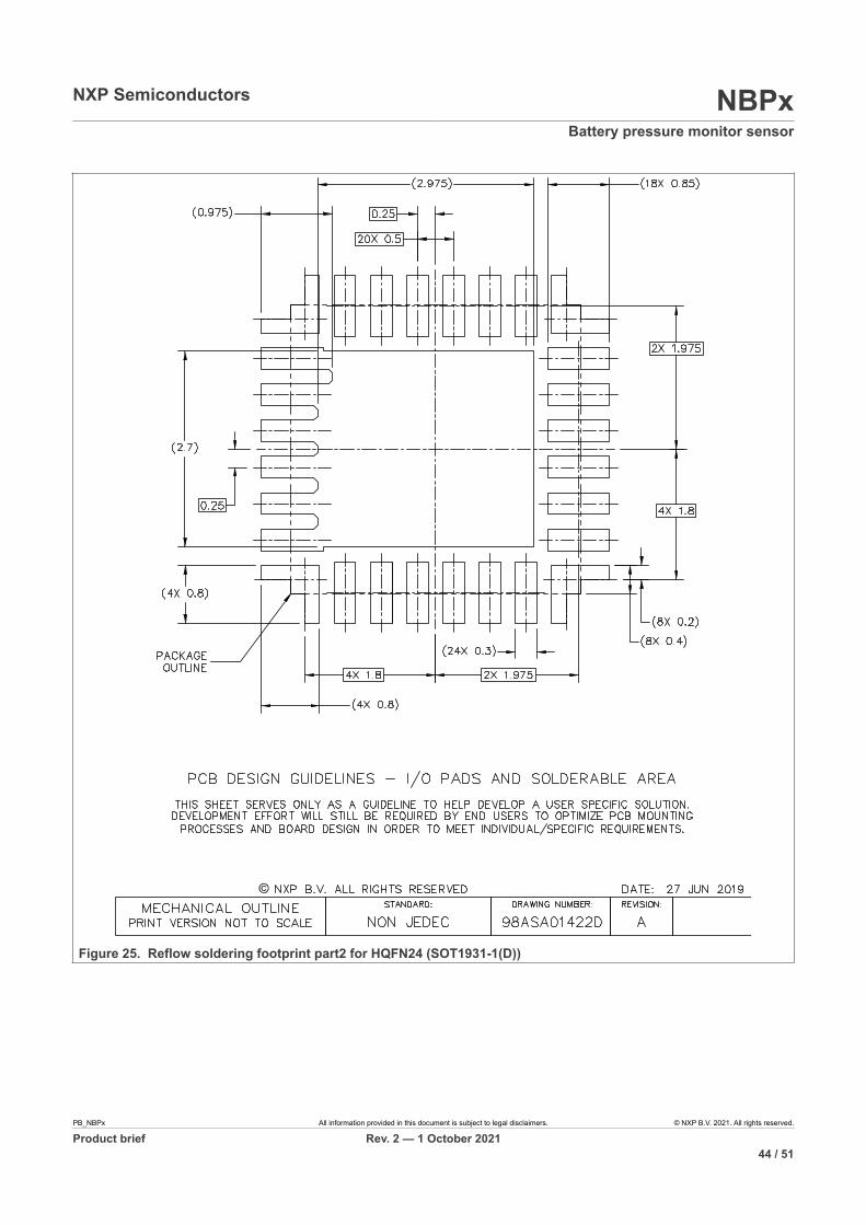
NXP Semiconductors NBPxBattery pressure monitor sensor
Figure 25. Reflow soldering footprint part2 for HQFN24 (SOT1931-1(D))
PB_NBPx All information provided in this document is subject to legal disclaimers. © NXP B.V. 2021. All rights reserved.
Product brief Rev. 2 — 1 October 202144 / 51

NXP Semiconductors NBPxBattery pressure monitor sensor
Figure 26. Reflow soldering footprint part3 for HQFN24 (SOT1931-1(D))
PB_NBPx All information provided in this document is subject to legal disclaimers. © NXP B.V. 2021. All rights reserved.
Product brief Rev. 2 — 1 October 202145 / 51

NXP Semiconductors NBPxBattery pressure monitor sensor
Figure 27. Package outline notes HQFN24 (SOT1931-1(D))
12 References
NXP reference documents
[1] NXP Specification NXPOMS-1719007347-3772, Media Test for Automotive Pressure Sensors
[2] AN1902, Assembly guidelines for QFN (quad flat no-lead) and SON (small outline no-lead) packages
PB_NBPx All information provided in this document is subject to legal disclaimers. © NXP B.V. 2021. All rights reserved.
Product brief Rev. 2 — 1 October 202146 / 51

NXP Semiconductors NBPxBattery pressure monitor sensor
13 Revision history
Rev Date Description
v.2 20211001 • Section 2, removed four features starting with "Power-up...", "Ultra-low...", "Temperature range..." and "PWM ouput.…"
• Section 3.1, revised as follows:– Figure 1, revised the image.– Table 1, added new row for "PTA4".
• Section 3.7.4, Table 3, revised the "ADC self-test duration value from"155" to "455".
• Section 5, revised as follows:– Table 44: revised "NBP8FDzT1" to "NBPxFD4T1" and removed the
second row in the table.– NBPx product code definition: revised the product code description
from "NBPxDzT1" to "NBPxFD4T1" and removed the descriptionsfor pressure error tolerance and standard/precision tolerances.
• Section 7.1, Figure 19, added additional content to the note.• Section 8.1, revised the section title from "Maximum ratings
(electrical)" to "Limiting values" to conform to NXP documentationguidelines.
• Section 8.2, revised the section title from "Operating conditions"to "Recommended operating conditions" to conform to NXPdocumentation guidelines and revised the "Max" value for "IDD1" from"11" to "18".
v.1 20201112 Initial release
Table 51. Revision history
PB_NBPx All information provided in this document is subject to legal disclaimers. © NXP B.V. 2021. All rights reserved.
Product brief Rev. 2 — 1 October 202147 / 51

NXP Semiconductors NBPxBattery pressure monitor sensor
14 Legal information
14.1 DefinitionsDraft — A draft status on a document indicates that the content is stillunder internal review and subject to formal approval, which may resultin modifications or additions. NXP Semiconductors does not give anyrepresentations or warranties as to the accuracy or completeness ofinformation included in a draft version of a document and shall have noliability for the consequences of use of such information.
14.2 DisclaimersLimited warranty and liability — Information in this document is believedto be accurate and reliable. However, NXP Semiconductors does notgive any representations or warranties, expressed or implied, as to theaccuracy or completeness of such information and shall have no liabilityfor the consequences of use of such information. NXP Semiconductorstakes no responsibility for the content in this document if provided by aninformation source outside of NXP Semiconductors. In no event shall NXPSemiconductors be liable for any indirect, incidental, punitive, special orconsequential damages (including - without limitation - lost profits, lostsavings, business interruption, costs related to the removal or replacementof any products or rework charges) whether or not such damages are basedon tort (including negligence), warranty, breach of contract or any otherlegal theory. Notwithstanding any damages that customer might incur forany reason whatsoever, NXP Semiconductors’ aggregate and cumulativeliability towards customer for the products described herein shall be limitedin accordance with the Terms and conditions of commercial sale of NXPSemiconductors.
Right to make changes — NXP Semiconductors reserves the right tomake changes to information published in this document, including withoutlimitation specifications and product descriptions, at any time and withoutnotice. This document supersedes and replaces all information supplied priorto the publication hereof.
Applications — Applications that are described herein for any of theseproducts are for illustrative purposes only. NXP Semiconductors makesno representation or warranty that such applications will be suitablefor the specified use without further testing or modification. Customersare responsible for the design and operation of their applications andproducts using NXP Semiconductors products, and NXP Semiconductorsaccepts no liability for any assistance with applications or customer productdesign. It is customer’s sole responsibility to determine whether the NXPSemiconductors product is suitable and fit for the customer’s applicationsand products planned, as well as for the planned application and use ofcustomer’s third party customer(s). Customers should provide appropriatedesign and operating safeguards to minimize the risks associated withtheir applications and products. NXP Semiconductors does not accept anyliability related to any default, damage, costs or problem which is basedon any weakness or default in the customer’s applications or products, orthe application or use by customer’s third party customer(s). Customer isresponsible for doing all necessary testing for the customer’s applicationsand products using NXP Semiconductors products in order to avoid adefault of the applications and the products or of the application or use bycustomer’s third party customer(s). NXP does not accept any liability in thisrespect.
Limiting values — Stress above one or more limiting values (as defined inthe Absolute Maximum Ratings System of IEC 60134) will cause permanentdamage to the device. Limiting values are stress ratings only and (proper)operation of the device at these or any other conditions above thosegiven in the Recommended operating conditions section (if present) or theCharacteristics sections of this document is not warranted. Constant or
repeated exposure to limiting values will permanently and irreversibly affectthe quality and reliability of the device.
Terms and conditions of commercial sale — NXP Semiconductorsproducts are sold subject to the general terms and conditions of commercialsale, as published at http://www.nxp.com/profile/terms, unless otherwiseagreed in a valid written individual agreement. In case an individualagreement is concluded only the terms and conditions of the respectiveagreement shall apply. NXP Semiconductors hereby expressly objects toapplying the customer’s general terms and conditions with regard to thepurchase of NXP Semiconductors products by customer.
No offer to sell or license — Nothing in this document may be interpretedor construed as an offer to sell products that is open for acceptance orthe grant, conveyance or implication of any license under any copyrights,patents or other industrial or intellectual property rights.
Suitability for use in automotive applications — This NXP product hasbeen qualified for use in automotive applications. If this product is usedby customer in the development of, or for incorporation into, products orservices (a) used in safety critical applications or (b) in which failure couldlead to death, personal injury, or severe physical or environmental damage(such products and services hereinafter referred to as “Critical Applications”),then customer makes the ultimate design decisions regarding its productsand is solely responsible for compliance with all legal, regulatory, safety,and security related requirements concerning its products, regardless ofany information or support that may be provided by NXP. As such, customerassumes all risk related to use of any products in Critical Applications andNXP and its suppliers shall not be liable for any such use by customer.Accordingly, customer will indemnify and hold NXP harmless from anyclaims, liabilities, damages and associated costs and expenses (includingattorneys’ fees) that NXP may incur related to customer’s incorporation ofany product in a Critical Application.
Export control — This document as well as the item(s) described hereinmay be subject to export control regulations. Export might require a priorauthorization from competent authorities.
Translations — A non-English (translated) version of a document is forreference only. The English version shall prevail in case of any discrepancybetween the translated and English versions.
Security — Customer understands that all NXP products may be subjectto unidentified or documented vulnerabilities. Customer is responsiblefor the design and operation of its applications and products throughouttheir lifecycles to reduce the effect of these vulnerabilities on customer’sapplications and products. Customer’s responsibility also extends to otheropen and/or proprietary technologies supported by NXP products for usein customer’s applications. NXP accepts no liability for any vulnerability.Customer should regularly check security updates from NXP and follow upappropriately. Customer shall select products with security features that bestmeet rules, regulations, and standards of the intended application and makethe ultimate design decisions regarding its products and is solely responsiblefor compliance with all legal, regulatory, and security related requirementsconcerning its products, regardless of any information or support that maybe provided by NXP. NXP has a Product Security Incident Response Team(PSIRT) (reachable at [email protected]) that manages the investigation,reporting, and solution release to security vulnerabilities of NXP products.
14.3 TrademarksNotice: All referenced brands, product names, service names andtrademarks are the property of their respective owners.
NXP — wordmark and logo are trademarks of NXP B.V.
PB_NBPx All information provided in this document is subject to legal disclaimers. © NXP B.V. 2021. All rights reserved.
Product brief Rev. 2 — 1 October 202148 / 51

NXP Semiconductors NBPxBattery pressure monitor sensor
TablesTab. 1. Connection pins description .............................. 2Tab. 2. List of the main software-implemented
features ..............................................................4Tab. 3. Summary of execution times ...........................19Tab. 4. Read and write addresses summary ...............20Tab. 5. SPI Operations (SPIOPS) (address
0x0038) ............................................................20Tab. 6. SPIOPS fields description ............................... 21Tab. 7. Pressure Sampling Period (PSP) (address
0x0050) ............................................................21Tab. 8. PSP fields description ..................................... 21Tab. 9. Self-Test Execution Period (STPER)
(address 0x0051) ............................................ 21Tab. 10. STPER fields description ................................ 22Tab. 11. PIN Configuration (PINCFG) (address
0x0052) ............................................................22Tab. 12. PINCFG fields description ...............................22Tab. 13. Interrupt pulse Trigger (INTTRIG) (address
0x0053) ............................................................22Tab. 14. INTTRIG fields description .............................. 22Tab. 15. Pressure Change Configuration (PCCFG)
(address $0054) .............................................. 23Tab. 16. PCCFG fields description ................................23Tab. 17. Status of the latest executions (STATUS)
(address 0x0055) ............................................ 24Tab. 18. STATUS fields description ...............................24Tab. 19. Sensor Status (SENSTATUS) (address
0x0056) ............................................................25Tab. 20. SENSTATUS fields description ........................25Tab. 21. Command (CMD) (address 0x0057) ............... 26Tab. 22. CMD fields description .................................... 26Tab. 23. Pressure Change Debounce Threshold
(PCDEBT) (address 0x0058) .......................... 27Tab. 24. PCDEBT fields description ..............................27Tab. 25. Pressure Change Fixed Threshold High
(PCFIXTH) (address 0x0059) ..........................27
Tab. 26. Pressure Change Fixed Threshold Low(PCFIXTL) (address 0x005A) ..........................27
Tab. 27. PCFIXTH/L fields description .......................... 27Tab. 28. Pressure Change Minimum Threshold
(PCMINT) (address $005B) .............................27Tab. 29. PCMINT fields description ...............................28Tab. 30. Pressure Change Relative Threshold High
(PCRELTH) (address $005C) ..........................28Tab. 31. Pressure Change Relative Threshold Low
(PCRELTL) (address $005D) .......................... 28Tab. 32. PCRELTH/L fields description ......................... 28Tab. 33. Pressure Change Slope Threshold High
(PCSLOPETH) (address 0x005E) ...................28Tab. 34. Pressure Change Slope Threshold Low
(PCSLOPETL) (address 0x005F) ....................28Tab. 35. PCSLOPETH/L fields description ....................29Tab. 36. Temperature measurement (TCODE)
(address $0070) .............................................. 29Tab. 37. TCODE fields description ................................29Tab. 38. Voltage measurement (VCODE) (address
$0071) ............................................................. 29Tab. 39. Voltage measurement fields description ..........30Tab. 40. Index of the pressure FIFO (INDFIFO)
(address $0075) .............................................. 30Tab. 41. INDFIFO fields description .............................. 30Tab. 42. Pressure FIFO (PFIFOH/Lx) (addresses
$0076 - $008D) ...............................................30Tab. 43. PFIFOH/Lx fields description ...........................30Tab. 44. Ordering options ..............................................31Tab. 45. Pin description .................................................33Tab. 46. Electrical and mechanical specification
note definition table .........................................38Tab. 47. Maximum ratings .............................................38Tab. 48. Operating range .............................................. 38Tab. 49. Maximum ratings .............................................39Tab. 50. General specifications ..................................... 40Tab. 51. Revision history ...............................................47
FiguresFig. 1. Connections between the NBPx and
external host ......................................................2Fig. 2. State-transition diagram .................................... 5Fig. 3. Fixed Threshold algorithm flow ......................... 7Fig. 4. Example of execution of the fixed threshold
algorithm ............................................................8Fig. 5. Relative threshold algorithm flow ...................... 9Fig. 6. Example of execution of the relative
threshold algorithm ..........................................10Fig. 7. Slope threshold algorithm flow ........................ 11Fig. 8. Example of slope threshold algorithm flow ...... 13Fig. 9. Pressure FIFO filled for the first 25 samples ... 14Fig. 10. SPI timing description when transfers are
requested by the external host via theWAKE-UP pin, with INTTRIG_INTPOL=1 ....... 15
Fig. 11. Example sequence leading to a clock faulterror on the NBP8 side ................................... 16
Fig. 12. SPI timing description when transfers arerequested by the NBPx via the INTpin, with PINCFG_PTB1CFG = 5 andINTTRIG_INTPOL=1 ....................................... 17
Fig. 13. Sequence of periodic events ...........................17Fig. 14. Sequence of events when NBPx notifies
the external host of an event and theexternal host clears the SPIOPS register ........ 18
Fig. 15. Sequence of events when NBPx notifiesthe external host of an event but theexternal host does not clear the SPIOPSregister .............................................................18
PB_NBPx All information provided in this document is subject to legal disclaimers. © NXP B.V. 2021. All rights reserved.
Product brief Rev. 2 — 1 October 202149 / 51

NXP Semiconductors NBPxBattery pressure monitor sensor
Fig. 16. External host requests SPI transfers andthen clears the SPIOPS register ..................... 19
Fig. 17. External host requests SPI transfers butdoes not clear the SPIOPS register ................ 19
Fig. 18. Block diagram ................................................. 32Fig. 19. Pin configuration ............................................. 33Fig. 20. NBP8 application .............................................36Fig. 21. NBP9 application .............................................37Fig. 22. Package outline HQFN24 (SOT1931-1(D)) ..... 41
Fig. 23. Package outline detail HQFN24(SOT1931-1(D)) ...............................................42
Fig. 24. Reflow soldering footprint part1 forHQFN24 (SOT1931-1(D)) ............................... 43
Fig. 25. Reflow soldering footprint part2 forHQFN24 (SOT1931-1(D)) ............................... 44
Fig. 26. Reflow soldering footprint part3 forHQFN24 (SOT1931-1(D)) ............................... 45
Fig. 27. Package outline notes HQFN24(SOT1931-1(D)) ...............................................46
PB_NBPx All information provided in this document is subject to legal disclaimers. © NXP B.V. 2021. All rights reserved.
Product brief Rev. 2 — 1 October 202150 / 51

NXP Semiconductors NBPxBattery pressure monitor sensor
Contents1 General description ............................................ 12 Features and benefits .........................................13 Operations ........................................................... 13.1 Communication between the NBPx and
external host ...................................................... 13.2 Serial peripheral interface (SPI) module ............33.3 Main features .....................................................43.4 State-transition diagram .....................................43.5 Pressure change detection description ..............53.5.1 Overview ............................................................53.5.2 Description of the fixed threshold option ............63.5.3 Description of the relative threshold option ........83.5.4 Description of the rate of change threshold
option ............................................................... 103.5.5 Description of the pressure FIFO .................... 133.6 SPI transfer sequence ..................................... 143.6.1 SPI transfer requested by the external host
via the WAKE-UP pin ...................................... 143.6.2 SPI transfer requested by the NBPx, when
an event requiring attention occurred .............. 163.7 Typical sequence timings ................................ 173.7.1 Periodic events ................................................ 173.7.2 NBPx notifying the external host ..................... 173.7.3 External host requesting an SPI transfer ......... 183.7.4 Summary of execution times ........................... 193.8 Read/write registers accessible by the
external host over SPI .....................................204 Applications .......................................................305 Ordering information ........................................ 316 Block diagram ................................................... 317 Pinning information .......................................... 327.1 Pinning .............................................................337.2 Pin description ................................................. 337.3 Applications ......................................................368 Electrical specifications ................................... 388.1 Limiting values .................................................388.2 Recommended operating conditions ............... 389 Mechanical specifications ................................399.1 Maximum ratings (mechanical) ........................399.2 Media compatibility .......................................... 4010 Mounting recommendations ............................ 4011 Package outline .................................................4012 References ......................................................... 4613 Revision history ................................................ 4714 Legal information ..............................................48
Please be aware that important notices concerning this document and the product(s)described herein, have been included in section 'Legal information'.
© NXP B.V. 2021. All rights reserved.For more information, please visit: http://www.nxp.comFor sales office addresses, please send an email to: [email protected]
Date of release: 1 October 2021Document identifier: PB_NBPx