pb-free electronics research manhattan project · ed morris (lockheed martin) & jerry aschoff...
TRANSCRIPT

Pb-free Electronics Research
“Manhattan Project”
Pb-free Electronics Research Manhattan Project
Technical Overview
Carmine Meola – et al
ACI Technologies
Pb-free Is Not Free!

Pb-free Electronics Research
“Manhattan Project”
Project Participants
• B2P COE Project Management: Carmine Meola
• Technical Project Leadership: Ed Morris (Lockheed Martin) & Jerry Aschoff (Boeing) –
Self-funded
• Meeting Moderator: Dr. Richard R. Reilly, Howe School of Technology Management, Stevens Institute of Technology
• SMEs:–
Dr. Peter Borgesen (Universal Instruments/Unovis)
–
Lloyd Condra (Boeing)–
Dr. Carol Handwerker (Purdue University)
–
Dr. Craig Hillman (DfR Solutions)–
Dave Hillman (Rockwell Collins)
–
Dave Humphrey (Honeywell)–
Dave Locker (AMRDEC)
–
Dr. Steph Meschter (BAE Systems)–
Dr. Mike Osterman (Univ. of Maryland CALCE)
–
Dave Pinsky (Raytheon)–
Dr. Tony Rafanelli (Raytheon)
–
Dr. Polina Snugovsky (Celestica)–
Fred Verdi (ACI)
–
Dr. Paul Vianco (Sandia National Labs)–
Maureen Williams (NIST)
–
Dr. Tom Woodrow (Boeing)–
Linda Woody (Lockheed Martin)

Pb-free Electronics Research
“Manhattan Project”
Discussion Topics
• Pb-free Electronics Manhattan Project Overview• Tin Whiskers• Manufacturing• Solder Reliability• Components• Printed Circuit Boards

Pb-free Electronics Research
“Manhattan Project”
Summary Approach for Aerospace & Defense (A&D) Pb-free Electronics Risk Reduction
20102010--20132013--------20092009
DoD plus…
Phase 1: Best Practice Baseline – Completed
Manhattan Project
ONR Funded
JDMTP FundedPhase 2: Technology Roadmap – In Work! Phase 3 – Integrated Risk
Reduction Projects
Pb-free Electronics Risk Reduction Program
•
Tin Whiskers•
Electronics Assembly
•
Solder Joints•
Electronic Component
•
Printed Circuit Boards
Manhattan Project A&D PbA&D Pb--free Electronics Projectfree Electronics Project
Customers

Pb-free Electronics Research
“Manhattan Project”
Who Decided to Remove the Pb?
• Reduction of Hazardous Substances (RoHS)–
EU Directive banning “placing on market”
new electronic equipment
containing specific levels of the following after July 1, 2006–
RoHS covers Lead, Cadmium, Mercury, hexavalent chromium, polybrominated biphenyl (PBB), polybrominated diphenyl ether (PBDE) flame retardants
• Waste Electrical and Electronic Equipment Directive (WEEE)–
EU directive aims to minimize the impact of electronic waste
– Encourages and sets criteria for collection, treatment, recycling
– Makes the producer responsible
• Related legislation in place in China, Japan, & Korea
Lead-free brings new and re-emerging failure modes in electronics

Pb-free Electronics Research
“Manhattan Project”
Why Is Pb Currently Used in Electronics?
•
Added to improve electronics reliability–
Improved Solderability
–
Inexpensive Solution–
Lower the solder melt temperature for improved component reliability
–
Stronger Solder Joints (Mechanical and Electrical Properties)–
Essentially eliminated the growth of tin whiskers that cause failures
Losing 50+ Years of Proven & Predictable Performance Using Tin-Pb Electronics
Photo Source: NASA GoddardPhoto Source: NASA Goddard
Tin Whiskers Growing on a Pure Tin ComponentTin Whiskers Growing on a Pure Tin Component

Pb-free Electronics Research
“Manhattan Project”
Where Is Pb Used in Electronics?
DIE DIEDIE
Internal to components:Die Bonding Lead Finish
Solder Ball Array
PWB / ComponentInterconnect
PWB Surface Finish
Component Terminations
Plating of Hardware on and around Circuit Cards

Pb-free Electronics Research
“Manhattan Project”
What Is the Difference Between Pure Tin vs. Pb-Free Electronics?
Pure Tin(Alloy with >97 wt % Sn)
Pb-Free(Alloy with <0.1 wt % Pb)
NiPdSn over Ni
Reflowed Sn
NiPdAu
Matte Sn
Bright Sn Annealed MatteSn
Hot Dipped Sn
SnBiCu
SnAg
NiAu SnBi
Hot-dipped SnCu
Hot-dipped SnAgCu
AgPd
Concerns:•Tin Whiskers•Tin Pest
Main Area Main Area of Past Focusof Past Focus
SnCu
Matte Sn over Ag
Hot-dipped SnAg
Ag
Annealed Matte SnCu
Pure Tin Requires Mitigation; Pb-Free Requires an Understanding of New Materials
Concerns:•
Reliability Data
•
Supply Chain Management / Configuration Control
•
Manufacturing Complexity
•
Field Support
Dominant Risk Dominant Risk AreaArea
SnAgNi

Pb-free Electronics Research
“Manhattan Project”
What Are the Pb-Free Electronics Concerns?
Cracked Solder Joint
•
Manufacturing–
Prevailing Pb-free solder replacement (SnAgCu) has ~35°C higher reflow temperature
–
Can affect components and board material–
Infant mortality / Latent failures
–
Requalification?•
Solder joint reliability (durability)–
Pb-free alloys can fail in high stress/strain applications
–
Intermetallics between solder and lead/pad–
Cross contamination of different alloys
–
Changed / unacceptable wetting characteristics–
New qualification parameters
•
Configuration Control–
Must prevent mixing of incompatible alloys
–
Many components not uniquely identified–
Field Support/Depot Repair Logistical Nightmare
Cracked Solder Joint

Pb-free Electronics Research
“Manhattan Project”
Pb-free Electronics Operating Environment vs. Operational Life-time
Operational Service Life (Years)
Har
shne
ss o
f Ser
vice
Env
ironm
ent
(Hum
idity
, Tem
pera
ture
, Sho
ck, V
ibra
tion)
Low
High
5 101 203 30
Con
sequ
ence
s of
Fai
lure
Tin Whiskers
Cell PhonesCell PhonesMajor Home Major Home AppliancesAppliances
CarsCars
SatellitesSatellitesMedical Medical EquipmentEquipment
AA BB
CC DD
Desktop PCsDesktop PCs
Network ServersNetwork Servers
MissilesMissiles
AircraftAircraft
A&D Risk ReductionProject Focus

Pb-free Electronics Research
“Manhattan Project”
Current Pb-free Electronics Technical Status
•
No universally acceptable technical solutions in sight to replace SnPb in Aerospace & Defense (A&D) applications–
Conformal coatings only mitigate tin whiskers
–
Pb-free solder joint reliability decreased for shock and has corrosion issues
–
SAC305 solder dissolves copper, impacting rework and repair–
Conductive Anodic Filament (CAF) problem is re-emerging due to higher CCA processing temperatures using Pb-free solders
•
Current technical approaches are all still “mitigations”
and not “elimination”
of the Pb-free electronics issues
Ref: “Lead Free PCBProjects Update,”
Wayne Jones,Advanced Research of
Electronic Assemblies Consortium,
February 2008
Conductive Anodic Filament (CAF) in
Circuit Card Assembly (CCA)
Pb-free Electronics Research
“Manhattan Project”
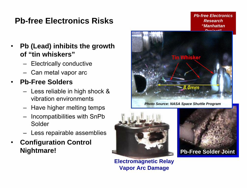
Pb-free Electronics Risks
• Pb (Lead) inhibits the growth of “tin whiskers”–
Electrically conductive
– Can metal vapor arc
• Pb-Free Solders–
Less reliable in high shock & vibration environments
– Have higher melting temps
– Incompatibilities with SnPb Solder
– Less repairable assemblies
• Configuration Control Nightmare!
Electromagnetic Relay Vapor Arc Damage
Pb-Free Solder Joint
Photo Source: NASA Space Shuttle Program
Pb-free Electronics Research
“Manhattan Project”
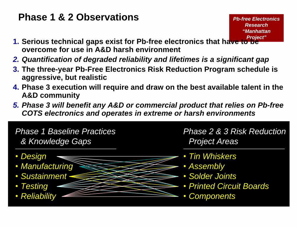
Phase 1 & 2 Observations
1. Serious technical gaps exist for Pb-free electronics that have to be overcome for use in A&D harsh environment
2. Quantification of degraded reliability and lifetimes is a significant gap3. The three-year Pb-Free Electronics Risk Reduction Program schedule is
aggressive, but realistic4. Phase 3 execution will require and draw on the best available talent in the
A&D community 5. Phase 3 will benefit any A&D or commercial product that relies on Pb-free
COTS electronics and operates in extreme or harsh environments
Phase 1 Baseline Practices & Knowledge Gaps
•
Design•
Manufacturing
•
Sustainment•
Testing
•
Reliability
Phase 2 & 3 Risk Reduction Project Areas
•
Tin Whiskers•
Assembly
•
Solder Joints•
Printed Circuit Boards
•
Components

Pb-free Electronics Research
“Manhattan Project”
1/28/10
Critical “ASAP” Steps Completed and In Work
• Pb-free Electronics Research “Manhattan Project”
Team
Benchmarking & Roadmapping
Study–
Phase 1: Identify current best practices to deal with Pb-free electronics (2 Weeks, 20 April to 1 May 2009) – Completed!
•
Funded by Navy ManTech Benchmarking & Best Practices Center of Excellence
•
Report available for download at the B2P COE Website (http://www.navyb2pcoe.org/b2p_news.html) and the Defense Acquisition University Lead-free Website (https://acc.dau.mil/leadfree)
–
Phase 2: Define the Risk Reduction Roadmap to address the gaps(2 Weeks, 17 – 28 August 2009) – In Work!
•
Funded by Joint Defense Manufacturing Technology Panel (JDMTP)•
Met for two weeks in August and developed a 36-month Risk Reduction Roadmap for Phase 3 execution
•
Report with Roadmap and ROM cost estimates being drafted – targeting early 2010 release
14Pb-Free Is Not Free!

Pb-free Electronics Research
“Manhattan Project”
Recommended Roadmap for A&D Pb-free Electronics Risk Reduction •
Coordinated approach proposed to achieve technical consensus–
Individual companies figuring out unique solutions will result in configuration, contractual and logistics nightmares
–
High cost if each individual company “figures this out”
on their own–
DoD readiness and sustainment will be severely impacted by a non-
coordinated approach
• 72 integrated project tasks have been defined–
Organized under the six major “project areas”
–
15 intermediate “project groups”–
Durations between 6 and 36 months
–
Most projects estimated to require between $500k and $1M
• Projects typically “collaborate”
with at least five other concurrent
projects
Pb-free Electronics Research
“Manhattan Project”
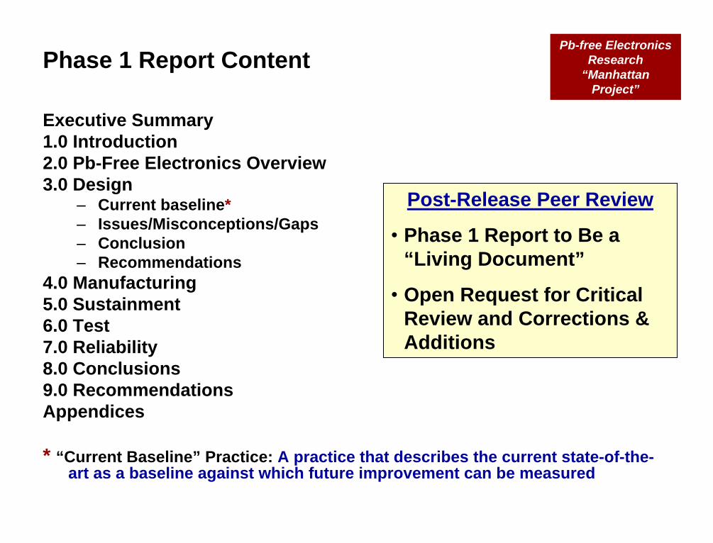
Phase 1 Report Content
Executive Summary1.0 Introduction2.0 Pb-Free Electronics Overview3.0 Design
–
Current baseline* –
Issues/Misconceptions/Gaps
–
Conclusion–
Recommendations
4.0 Manufacturing5.0 Sustainment6.0 Test7.0 Reliability8.0 Conclusions9.0 RecommendationsAppendices
* “Current Baseline” Practice: A practice that describes the current state-of-the- art as a baseline against which future improvement can be measured
Post-Release Peer Review
•
Phase 1 Report to Be a “Living Document”
•
Open Request for Critical Review and Corrections & Additions

Pb-free Electronics Research
“Manhattan Project”
KEY DELIVERABLES•
Detailed Design Guidelines
•
Validated Life-Prediction Models•
Assembly and Repair Process Definitions
•
Methodologies for Assessing New Materials
Recommended Roadmap for A&D Pb-free Electronics Risk Reduction (Cont’d)
Tin Whiskers
Solder Joint Reliability
Manufacturing and Repair Processes
Component Issues
Program Management/Coordination
PCB Issues
Pb-free Electronics Risk Reduction
Year 3Year 2Year 1
Interconnection Reliability
Tin Whisker Risk Mitigation
17

Pb-free Electronics Research
“Manhattan Project”
Any Recent Failures?SAC BGA Rework “Head in Pillow (HiP)”
Defect
• Problem: Intermittent ATC open failure after rework (2000 I/O BGA with 1 open joint)
• Lab Analysis: Metallurgical analysis found “head-on-pillow”
and differential cooling
between balls and paste•
Result: SAC process requires regular calibration of reflow heaters
• Other Causes: BGA ball contamination, warpage
Paste & SAC Ball Not Wetted
Large Sn Dendrite Indicates Slower Cooling
at Component SideSAC Paste Resolidified
Before Wetting to BGA
BGA Ball Open (HiP) 3D X-ray Reconstruction Photos Provided by Celestica
1/28/10 18Pb-Free Is Not Free!

Pb-free Electronics Research
“Manhattan Project”
Any Recent Failures? (Cont’d)A Recent Industry Disclosure:1.
A board assembly house working on an Defense development Contract
who was
successfully soldering lead-free BGAs of around 1000 balls onto a tin lead PCB got into a problem recently.
2.
The board assembler developed an oven profile which soldered the
SAC 305 BGAs and the tin-lead with out damaging temperature sensitive components.
3.
Everything was going along well until the manufacturer of the BGAs switched from SAC 305 to SAC 105 because of concerns about solder fracture during drop testing from commercial customers.
4.
The BGA had the same lead-free logos on it indicating it was RoHS compliant. The markings did not reflect the alloy change of the BGA solder balls.
5.
SAC 305 has a melting temp of around 221C. SAC105 has a melting
temperature of 228C.
6.
The profile that melted the SAC 305 BGAs did not fully melt all the SAC 105 BGA solder balls.
7.
The problem was missed until an intermittently functioning BGA was found during trouble shooting.
The BGA passed automated X-ray inspection. The connections were
in the middle of the package and not optically inspectable. 8.
Unfortunately some of the product escaped into the field and had
to be recalled.
1/28/10 Pb-Free Is Not Free! 19

Pb-free Electronics Research
“Manhattan Project”
Tin Whiskers
20

Pb-free Electronics Research
“Manhattan Project”
What Is a “Tin Whisker”?
•
Tin whisker effects documented since the 1940’s•
Tin Whiskers–
Occur on nearly all tin alloys
–
Few microns to ½
inch +–
Electrically conductive
•
Hardware–
Tin plated nuts, bolts, covers, card guides, etc. also at risk
•
Whisker Induced Failures:–
Short Circuit: Bridges two adjacent pins
–
Metal vapor arc: Voltage and atmospheric conditions can result in plasma arc capable of catastrophic damage
–
FOD: Whisker breaks off and interferes with mechanical, optical, or MEMS component
1/31/3 inchinch
Photo Source: NASA Space Shuttle Program

Pb-free Electronics Research
“Manhattan Project”
12/3/09 Pb-Free Is Not Free! 22

Pb-free Electronics Research
“Manhattan Project”
Have Tin Whiskers Caused Failures?
•
Multiple Documented Occurrences (NASA/Industry/Academic Publications)–
Nuclear Utilities
–
7 Satellites ($100M Boeing Loss)–
Patriot (PAC-2)
–
6 Missile Programs –
Heart Pacemaker
– F-15 Radar
– Military Airplane
– Telecom. Equip.
$1B Worth of Satellites, Missiles & Other Equipment
NOTE: Electromagnetic Relay Was Purchased to MIL Spec Prohibiting Pure Tin Finish Inside, But IT WAS Pure Tin
Ref: http://Ref: http://nepp.nasa.gov/whisker/failures/index.htmnepp.nasa.gov/whisker/failures/index.htm
Catastrophic Damage Due to Tin Whisker Induced Metal Vapor Arc

Pb-free Electronics Research
“Manhattan Project”
How Can We Mitigate Tin Whiskers?
Growing on Reworked Component Lead
Tin Whisker Examples
Growing on Capacitor
•
Design Practices–
Eliminate exposed conductive surfaces
–
Conformal Coating•
Material Selection –
Avoid Use of Tin Plating Greater than 97% Purity
•
Component & Assembly Processes–
Re-flow of Pure Tin Plated Surfaces
–
Solder Dip / Strip & Re-plate Terminations
–
Annealing•
Handling Practices–
Provide Stable Storage Environment
–
Temperature/Humidity–
Provide Protection From Mechanical Damage
•
Mitigation ≠
Elimination

Pb-free Electronics Research
“Manhattan Project”
12/3/09 Pb-Free Is Not Free! 2525

Pb-free Electronics Research
“Manhattan Project”
Manufacturing and Repair
26

Pb-free Electronics Research
“Manhattan Project”
12/3/09 Pb-Free Is Not Free! 27
The Pb-free Impact on the Manufacturing Process Flow
Manufacturing Flow
Purchase and Store Parts/Boards
Incoming InspectionPaste Print
(4.4)
Chip Adhesive Application
(4.5)
Clean & Mark(4.9)
Inspect(4.11)
Kit and Issue to Production
Test (in circuit)(4.14)
Convection Reflow(4.7)Part Placement
(4.5)
Test(ESS)(4.14)
Wave Solder(4.7)
Depanel(4.8)
Vapor Phase Reflow(4.7)
Selective Solder(4.7)
Conformal Coating(4.13)
Conformal Coating(4.13)
Pack & Ship(4.15)
DFM(4.2)
No Impact Low Impact High Impact
(Staging 4.3)
Rework(4.12)
Underfill(4.10)
(Solder Formation 4.6)

Pb-free Electronics Research
“Manhattan Project”
Solder Process Requires Higher Temperature Profiles
12/3/09 Pb-Free Is Not Free! 28

Pb-free Electronics Research
“Manhattan Project”
12/3/09 Pb-Free Is Not Free! 29
Current Baseline Practices
• Aerospace & Defense Manufacturing Processes which use Lead-free require tighter process controls and detailed process validation
•
Critical process parameters requiring tighter control include reflow profiles, cleaning requirements, and damage control margins due to higher processing temperatures.
•
Process variations may have a greater impact on resulting solder joint integrity
• Master manufacturing facility layout strategy required for coexistence or segregation of SnPb and Lead-free processes.
• Marking strategies and tighter inventory controls need to be adopted to distinguish SnPb from Lead-free (IPC-609).
• Basic understanding of metallurgy of different solder alloys and
subsequent solder joint integrity required•
Operator training is critical for process and inspection techniques

Pb-free Electronics Research
“Manhattan Project”
Solder Reliability
30

Pb-free Electronics Research
“Manhattan Project”
Solder Joint Reliability
• Majority of electronic part (memory, logic, passives, etc.) manufacturers have converted parts construction to comply with government regulations (i.e. EU RoHS). While some still provide
tin-
lead terminations, obtaining originally manufactured parts with tin- lead terminals is becoming increasingly difficult.
• For solder joint reliability, the greatest issue with maintaining tin-lead soldered assemblies is the increased use of area array packages which are no longer available with tin-lead solder bumps.
• Mixed solder (lead-free area array bumps and tin-lead solder paste) joints have known reliability issues which are dependent on the solder assembly process. This issue is further complicated by continued changes to solder composition by electronic part manufacturers.
• Conversion to full lead-free assemblies raises long-term reliability concerns. Again, this issue is further complicated by continued
changes by electronic part manufacturers.12/3/09 Pb-Free Is Not Free! 31

Pb-free Electronics Research
“Manhattan Project”
Solder Joint Project Area
• Solder Joint Reliability Models
• Effects Issue Resolution
• Underfill, Staking, and Coating Models
• Solder Selection Guidelines
• Insertion Mount Issue Resolution
• Handling Guidelines
12/3/09 Pb-Free Is Not Free! 32

Pb-free Electronics Research
“Manhattan Project”
Solder Joint Reliability Models
Provide (i) credible models for assessing life expectancy of solder interconnects formed with a set of prevalent solder combinations and (ii) optimized test methodology to qualify new solder combinations.
– Create common test vehicles
– Create common material database
– Create common failure database
•
Temperature cycling•
Vibration
•
Drop and Shock•
Combined Loads
– Create models based on common material and failure database
12/3/09 Pb-Free Is Not Free! 33

Pb-free Electronics Research
“Manhattan Project”
Mixed (lead-free bumped array assembled with Tin- lead solder paste) Solder
12/3/09 Pb-Free Is Not Free! 34
A SAC BGA was assembled in a conventional Sn37Pbsolder process. Failure in temperature cycling (-55 to 125oC) occurred in less than 150 cycles. This type of defect could escape current screening practices and result in aborted or failed missions.
Hillman, D., Wells, M., and Cho, K., “The Impact of Reflowing a Pb-free Solder Alloy Using A Tin/Lead Solder Alloy Reflow Profile on Solder Joint Reliability”
http://www.aciusa.org/lfpdf/lfjournal/CMAP_paper_Rev_A_(2).pdf
Last Accessed 1/22/2006

Pb-free Electronics Research
“Manhattan Project”
Tin-Silver-Copper Solder
12/3/09 Pb-Free Is Not Free! 35
‘As-fabricated’
BGA SAC Joints
100 μm
Sundelin, 2007
Park et al, , 2008
Park et al, , 2008
Bieler, 06E
, CTE
E, CTE
Significant scatter expected in SAC properties because
of heterogeneity & uniqueness caused by few large anisotropic Sn grains
Tin-Silver-Copper (SAC) alloys have gained market share as the lead-
free replacement for tin- lead solder. While select
compositions (i.e.95.5- 96.5Sn4.0-3.0Ag0.5Cu)
have been extensively studied, reliability concerns have resulted in continued exploration of new compositions.

Pb-free Electronics Research
“Manhattan Project”
3
1Elastic
ε
el =
σ/Ε
Plastic
ε
p = Kp
(T) σ
np(T)
Creep
ε
cr
= Kc
σ
nc
e-Δ Η / R
Τ
Constitutive laws
•
2 Package Architecture / Loads
UeWpWc
Nfe
, Nfp
, NfcOutput: Cycles to failure:
Overall Approach for Fatigue Life Prediction
Nfe NfcNfp
1 11 ++Nftotal
1=
Local Stress-Strain HistoryDamage Assessment
Cycles
Ene
rgy
dens
ity (M
Pa/
cycl
e)
Shear strain (%)
shea
r stre
ss (M
pa)
time
Tem
p. (C
)
A
B
Silicon die
Copper track
Passivationlayer
bondpad
metallization
solder joint
FR4 board
Package Architecture
Solderresist
4
*Figures and Images courtesy of CALCE, University of Maryland
36

Pb-free Electronics Research
“Manhattan Project”
Fatigue Damage Evolution
12/3/09 Pb-Free Is Not Free! 37
Sn37Pb SACUnder cyclic stress tin-lead solder exhibits grain coarsening (enlargement), crack formation and growth. For lead-free SAC solder, the structure exhibits
grain formation due to recrystalization
which results in finer grains that separate at grain boundaries resulting in crack growth. Due to anisotropic behavior and random dispersion of intermetallic compounds in the
solder,
material behavior exhibits a greater degree of randomness than occurred with SnPb.
*Images courtesy of CALCE, University of Maryland

Pb-free Electronics Research
“Manhattan Project”
Effects Issues
12/3/09 Pb-Free Is Not Free! 38
• Electromigration
– Current densities of 104A/cm2
create structural changes in solder material. Current
limits and impact on solder joint reliability need to be determined.•
Corrosion
– Impacts of corrosive environments on lead-free solder have been largely unexplored. Increased rate of damage due to corrosion may be a factor in extended service life.
• Board Finish
– Pad finish plays largely a secondary role but needs to be addressed to provide guidelines for designers.
• Solder Paste Evaluation
– Level of impact due to proprietary organics in solder pastes from different solder manufacturers not quantified.
• Wave Solder Contamination
– Visual defects may not be sufficient to determine acceptable contamination levels for wave solder. Life impact needs to be examined.
• Tin Pest
– Conversion of β-tin to α-tin. α-tin is highly brittle and falls apart under minimal loading. Transition known to occur a low temperatures (<13C). Factors that promote transitions and likelihood of issue remain unknown for long-term applications.
Pb-free Electronics Research
“Manhattan Project”
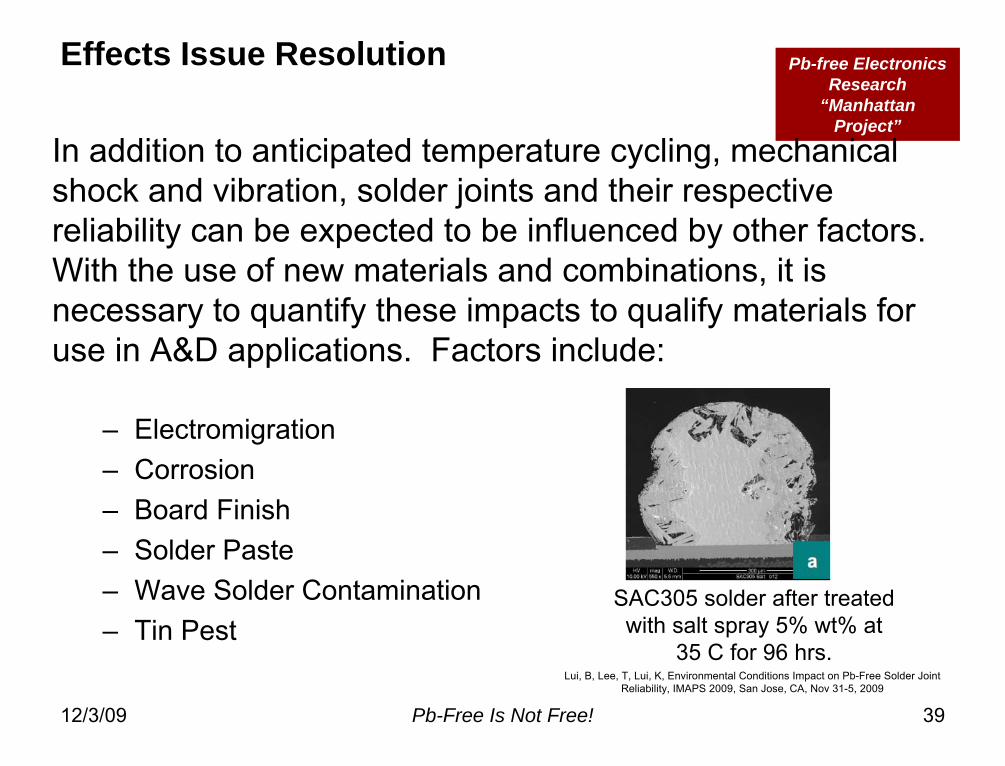
Effects Issue Resolution
In addition to anticipated temperature cycling, mechanical shock and vibration, solder joints and their respective reliability can be expected to be influenced by other factors. With the use of new materials and combinations, it is necessary to quantify these impacts to qualify materials for use in A&D applications. Factors include:
– Electromigration
– Corrosion
– Board Finish
– Solder Paste
– Wave Solder Contamination
– Tin Pest
12/3/09 Pb-Free Is Not Free! 39
SAC305 solder after treated with salt spray 5% wt% at
35 C for 96 hrs.Lui, B, Lee, T, Lui, K, Environmental Conditions Impact on Pb-Free Solder Joint
Reliability, IMAPS 2009, San Jose, CA, Nov 31-5, 2009

Pb-free Electronics Research
“Manhattan Project”
Testing
• Temperature Cycling–
Low strain rates, Low cycle
• Vibration–
High strain rates, High cycle
• Combined–
Mixed failure models produced by combination of low and high strain rates. Concerns with how to account for different combinations
• Drop and Shock–
Extremely high strain rates
• Creep Rupture–
Abrupt failure of joints under a fixed load.
12/3/09 Pb-Free Is Not Free! 40

Pb-free Electronics Research
“Manhattan Project”
Components
41

Pb-free Electronics Research
“Manhattan Project”
12/3/09 Pb-Free Is Not Free! 42
Components - Current Baseline Practices
• Component Pb-free process/materials compatibility characterized mainly for consumer applications
• Component Assembly Compatibility–
Moisture Sensitivity Level widely characterized for Pb-free
•
SnPb finishes not characterized for Pb-free process temperatures–
Temperature Sensitivity per J-STD-075 not universal
– Storage of components not major concern for most current Pb-
free applications–
No-clean processes for consumer items
• Component Finish Effects on Solder Joint Reliability–
Short term life generally sufficient for most finish materials

Pb-free Electronics Research
“Manhattan Project”
Components - Knowledge Gaps
• Assembly Process Temperature sensitivity
• Corrosion sensitivity–
Flux and cleaning compatibility
• Finish effects on solder joint reliability
• Solderability requirements
• Refinishing cost and schedule impacts
• Storage requirements for solderability maintenance
• Protocols for finish material verification
12/3/09 Pb-Free Is Not Free! 43
Uncertainties for Aerospace and Defense Applications

Pb-free Electronics Research
“Manhattan Project”
Components - R&D Approach Recommended Projects
• Component Characterization–
Temperature exposure limits
– Receiving/incoming inspection requirements
– Storage requirements for unassembled components
– Component properties database
– Fluxes/cleaning process compatibility with components
• Component Refinishing/Reprocessing
• Temperature Sensitivity Capability Improvement
• Component Finish–
Finish Solder Joint Effect
– Solderability
• Component Corrosion–
Corrosion Acceleration Factors
– Corrosion Mitigation
12/3/09 Pb-Free Is Not Free! 44
Pb-free Electronics Research
“Manhattan Project”
Printed Circuit Boards
45

Pb-free Electronics Research
“Manhattan Project”
Current Baseline Practices
• The printed circuit board is the foundation for the entire printed circuit assembly – if the PCB integrity is questionable, then all
other efforts are a moot point
Military/Aerospace Electronic Products Characterization:•
Life Critical & Flight Critical Applications
• Extremely Stable Qualified Material Lists
• Significant Use Life ~ 20-30 Years Not Uncommon
• Manufacturing Mode: High Mix/Low Volume
• Design Cycle Mode: Deliberate and Long ~ 12 Months
• Customer Certification
46

Pb-free Electronics Research
“Manhattan Project”
Knowledge Gap #1
• Printed Circuit Board Copper Structures:–
Pad Design/ Stencil Design Assessment and Confirmation
•
What pad patterns and stencil designs are required for the creation of High Performance solder joint geometries?
– Copper Requirements and Copper Dissolution
•
What are the minimum copper plating requirements for High Performance harsh environment integrity?
– Acceptance Test Methods for Void Formation associated with Aging of Solder/Copper Plated Structures
•
What test methods provided an assessment of void formation in solder/copper plated structures
47

Pb-free Electronics Research
“Manhattan Project”
Knowledge Gap #1
Copper Dissolution of Plated Thru Hole
48

Pb-free Electronics Research
“Manhattan Project”
Knowledge Gap #2
• Printed Circuit Board Laminate Materials:–
Thermal Robustness of Laminate Material
•
What level of laminate robustness is required to avoid thermally induced degradation in High Performance PCB laminates?
– Pad Cratering
•
How do we characterize, assess and design for a new failure mode in High Performance PCB laminates?
– Conductive Anodic Filament (CAF)
•
How do we characterize, assess and design for this failure mode in High Performance PCB laminates?
– Development of New Laminate Material
•
Application of High Performance PCB laminate key characteristics for laminate development
49

Pb-free Electronics Research
“Manhattan Project”
Knowledge Gap #2
Pad Cratering Defects (Courtesy of Celestica)
50

Pb-free Electronics Research
“Manhattan Project”
Knowledge Gap #3
• Printed Circuit Board Surface Finishes:–
Surface Finish Evaluation
•
What Assembly Robustness, Corrosion, Solderability and Tin Whisker characteristics are necessary requirements for High Performance Assembly Processes
– Surface Finish Test Methods
•
What test methods exist for understanding surface finish characteristics relating to harsh long storage and fielded environments
– Development of New PCB Plating Materials
•
Development of new plating materials that meets the assembly, reliability, and cost expectations of High Performance products
– Sporadic Brittle Failure of Pb-Free Solder Due to Nickel Plating
•
How do we characterize, assess and design for a new failure mode in High Performance PCB laminates
51
Pb-free Electronics Research
“Manhattan Project”
Knowledge Gap #4
• Printed Circuit Board Database and Design Rules:
– Heuristic rules used by electrical and mechanical designers based on experience with SnPb programs may be insufficient to ensure reliability of Pb-free product.
– Provide a database of new and future materials attributes and compatibilities resulting in design rules for PCBs used in Pb-free assembly of High Performance products.
52
Pb-free Electronics Research
“Manhattan Project”
Summary
•
Pb-free electronics are fundamentally and drastically changing the way electronic products for A&D are designed, procured, manufactured, tested, and supported
•
Need a coordinated, proactive DoD-wide Pb-free Electronics Risk Reduction Program
to deal with the issues and ensure
highest quality, best value electronic products for the Warfighter
•
The “Cultural Issues”
for Pb-free Electronics
are as challenging as the Technical Issues, making it more difficult to obtain risk
reduction funding
•
Good News: The “Manhattan Project”
concept has been validated as a viable approach to deal with complex issues that demand a radical approach –
A focused team of Government
and Industry Subject Matter Experts is recommended!