pb-free bgas in snpb assemblies projectthor.inemi.org/.../pb-free_bgas_snpb_assy.pdf ·...
TRANSCRIPT

Pb-Free BGAs inSnPB Assemblies
Project
Project Chair: Robert Kinyanjui,Ph.D. Sanmina-SCI Corporation
Project Co-Chair: Quyen Chu,
Jabil
Celestica-iNEMITechnology Forum
May 15, 2007

1
Project FormationProject Formation
Drivers
• Chairs (Jerry G. - HP and Charlie R. - IBM) and sub projectteam leaders (Jasbir B. – Solectron, Matt K. – Celestica andQuyen C. – Jabil) from the Lead-Free Assembly & ReworkProject identified a need to address backward compatibilityas project was near completion
• 2004 Roadmap identified a gap for process solution of Pb-free BGA in a SnPb process
• In November 2004, the backward compatibility project waslaunched….
2
Project ScopeProject Scope
• For companies choosing to take the RoHS exemption and
continue to manufacture SnPb products beyond July 1,
2006, there is a growing issue with the lack of availability of
SnPb components. Many companies may be compelled to
use Pb-free BGAs in a SnPb process, for which the process
and reliability have not yet been characterized.
3
ObjectivesObjectives
• Phase 1
– To assess the process parameters for assembling Pb-free SnAgCu BGAs under the
temperature constraints of a conventional tin-lead (SnPb) assembly process.
• Phase 2
– Characterize homogeneity of Pb-free BGAs in a SnPb process with the following
considerations:
– Package size/ball volume
– Reflow temperature
– Time above liquidus
– Solder paste volume
– Examine the thermal and mechanical reliability of Pb-free BGAs in SnPb process
• Phase 3
– To develop a “generic” process guideline and risk assessment for assembling Pb-free
BGAs in a SnPb assembly process.

4
3Perimeter80.5132A-CTBGA132-0.5mm-8mm
3Array190.8288A-CABGA288 0.8mm-19mm
3Perimeter231.00324A-PBGA324-1.0mm-23mm
3Perimeter451.27600A-SBGA600-1.27mm-45mm
Quantity
per
Board
Ball AlignmentSize
(mm)
Pitch
(mm)
I/OComponent Part
Numbers
Note:
• SnPb components
of each type were
used for baseline
run.1.0mm
PBGA324
0.8mm
CABGA
0.5mmCTBGA132
1.27mm
SBGA600
Pb-free BGA ball alloy: SAC405
Components ConsiderationComponents Consideration
5
PCB LaminatePCB Laminate
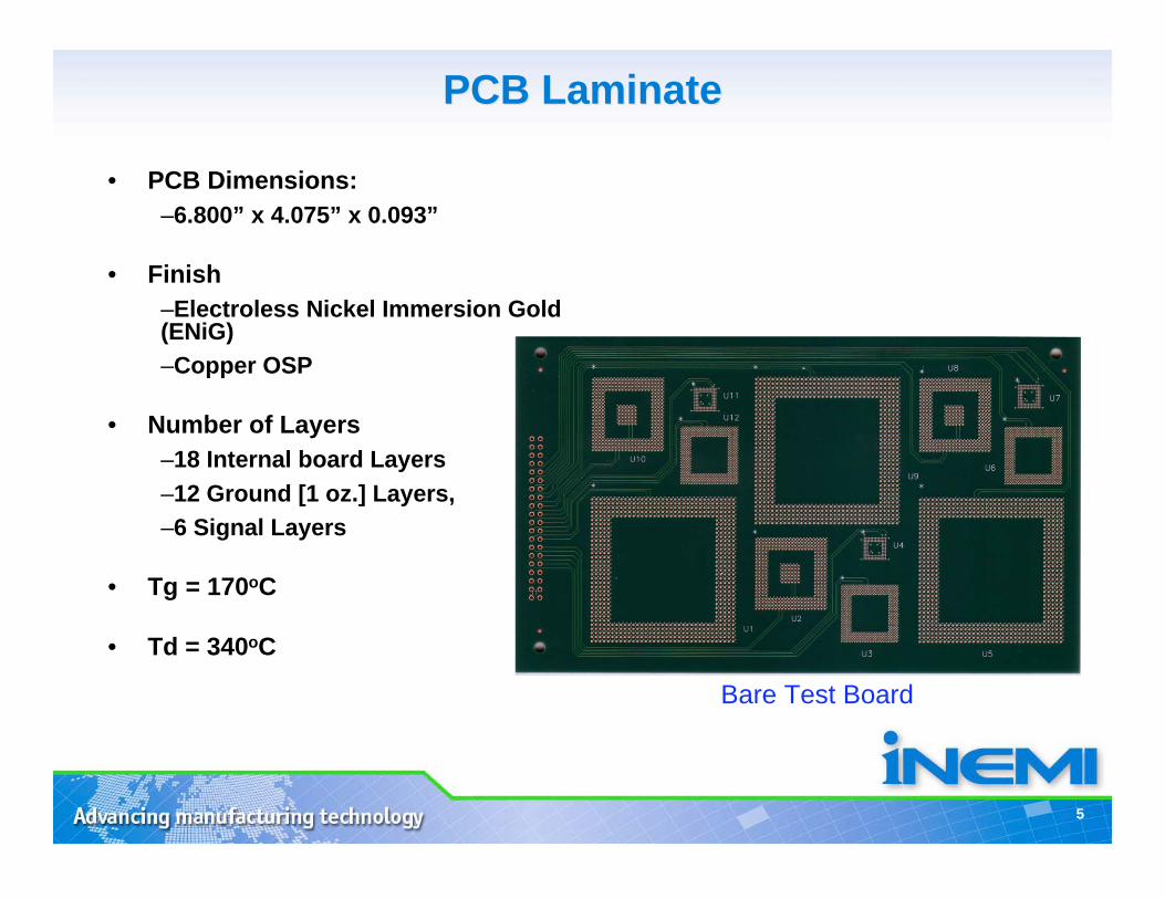
• PCB Dimensions:
–6.800” x 4.075” x 0.093”
• Finish
–Electroless Nickel Immersion Gold(ENiG)
–Copper OSP
• Number of Layers
–18 Internal board Layers
–12 Ground [1 oz.] Layers,
–6 Signal Layers
• Tg = 170oC
• Td = 340oC
Bare Test Board
6
Assembly ConsiderationAssembly Consideration
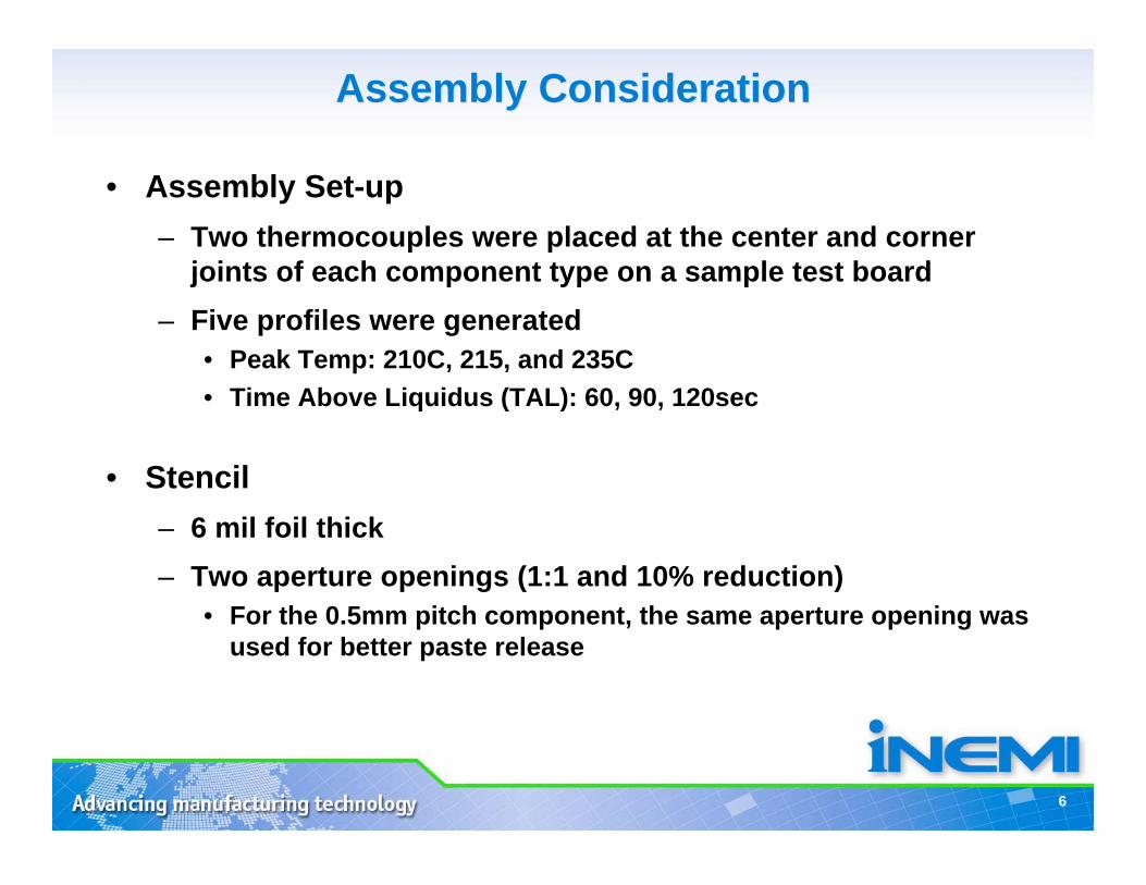
• Assembly Set-up
– Two thermocouples were placed at the center and corner
joints of each component type on a sample test board
– Five profiles were generated
• Peak Temp: 210C, 215, and 235C
• Time Above Liquidus (TAL): 60, 90, 120sec
• Stencil
– 6 mil foil thick
– Two aperture openings (1:1 and 10% reduction)
• For the 0.5mm pitch component, the same aperture opening was
used for better paste release
7
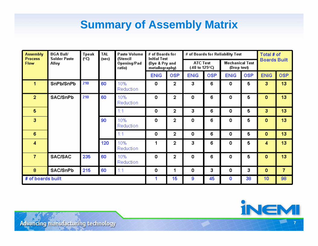
Summary of Assembly MatrixSummary of Assembly Matrix
8
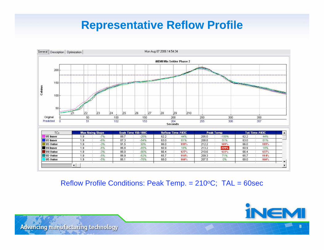
Representative Reflow ProfileRepresentative Reflow Profile
Reflow Profile Conditions: Peak Temp. = 210oC; TAL = 60sec
9
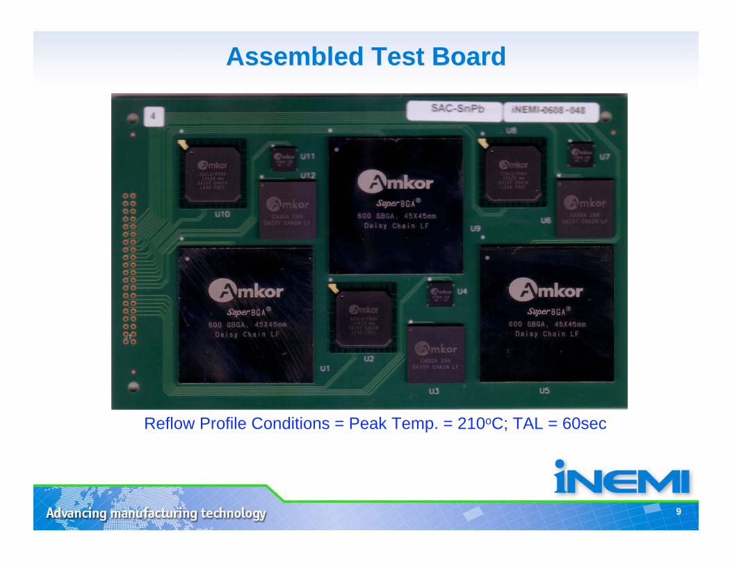
Assembled Test BoardAssembled Test Board
Reflow Profile Conditions = Peak Temp. = 210oC; TAL = 60sec
10
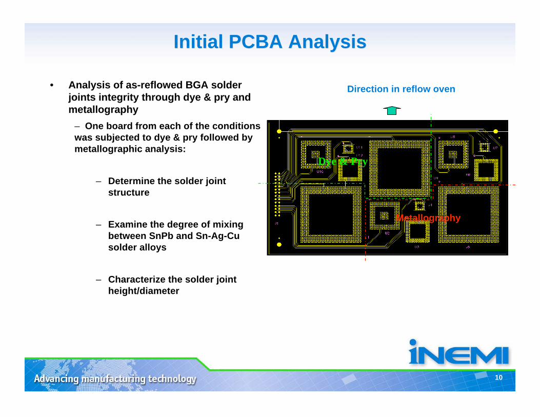
Initial PCBA AnalysisInitial PCBA Analysis
• Analysis of as-reflowed BGA solder
joints integrity through dye & pry and
metallography
– One board from each of the conditions
was subjected to dye & pry followed by
metallographic analysis:
– Determine the solder joint
structure
– Examine the degree of mixing
between SnPb and Sn-Ag-Cu
solder alloys
– Characterize the solder joint
height/diameter
Dye & Pry
Metallography
Direction in reflow oven
11
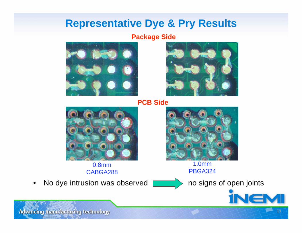
Representative Dye & Pry ResultsRepresentative Dye & Pry Results
1.0mm
PBGA3240.8mm
CABGA288
PCB Side
Package Side
• No dye intrusion was observed no signs of open joints
12
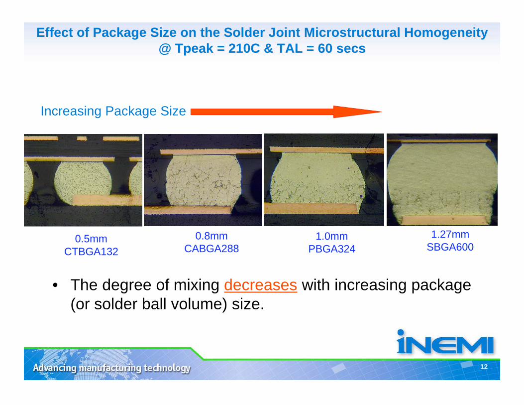
• The degree of mixing decreases with increasing package
(or solder ball volume) size.
1.0mm
PBGA324
1.27mm
SBGA6000.5mm
CTBGA132
0.8mm
CABGA288
Increasing Package Size
Effect of Package Size on the Solder Joint Effect of Package Size on the Solder Joint MicrostructuralMicrostructural Homogeneity Homogeneity
@ @ TpeakTpeak = 210C & TAL = 60 = 210C & TAL = 60 secssecs
13
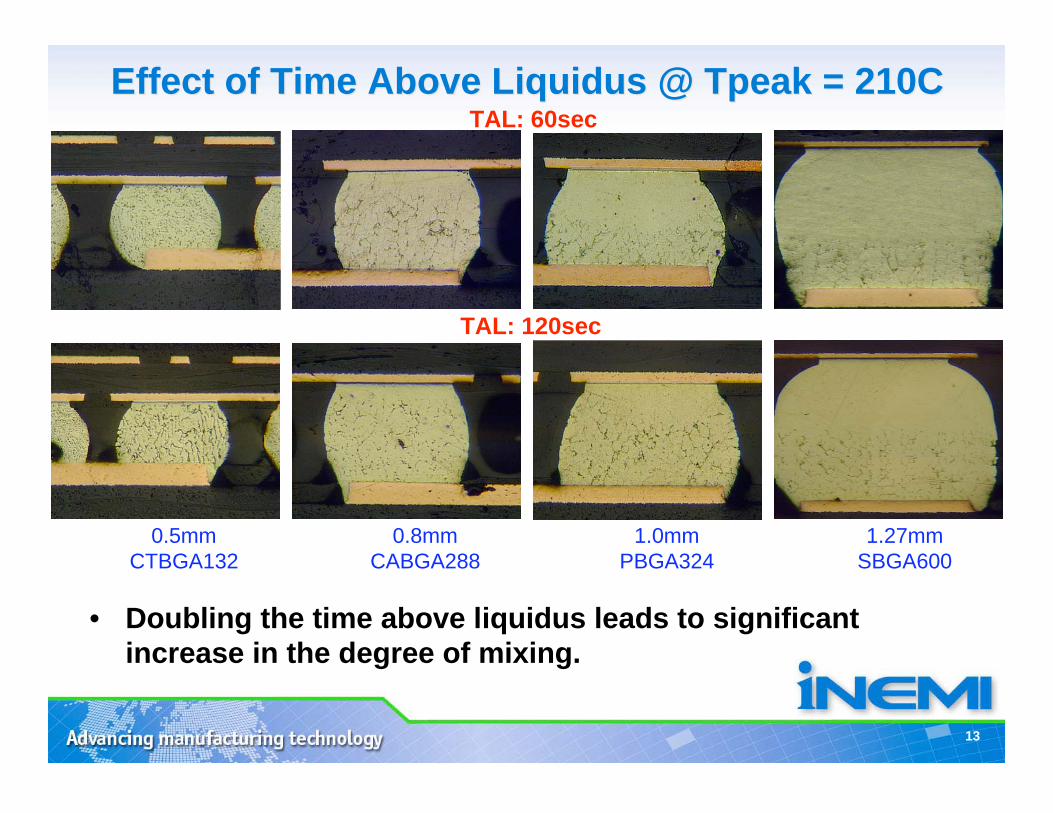
Effect of Time Above Effect of Time Above LiquidusLiquidus @ @ TpeakTpeak = 210C = 210C
• Doubling the time above liquidus leads to significant
increase in the degree of mixing.
1.0mm
PBGA324
1.27mm
SBGA600
0.5mm
CTBGA132
0.8mm
CABGA288
TAL: 120sec
TAL: 60sec
14
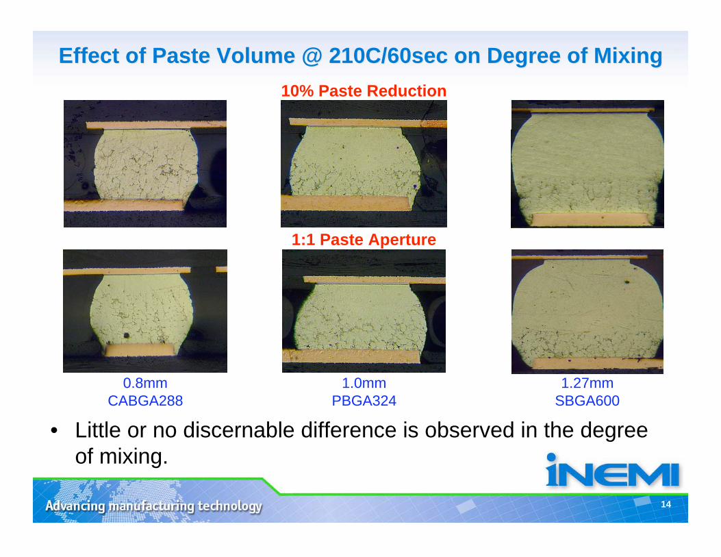
Effect of Paste Volume @ 210C/60sec on Degree of MixingEffect of Paste Volume @ 210C/60sec on Degree of Mixing
10% Paste Reduction
1:1 Paste Aperture
• Little or no discernable difference is observed in the degree
of mixing.
1.0mm
PBGA324
1.27mm
SBGA600
0.8mm
CABGA288
15
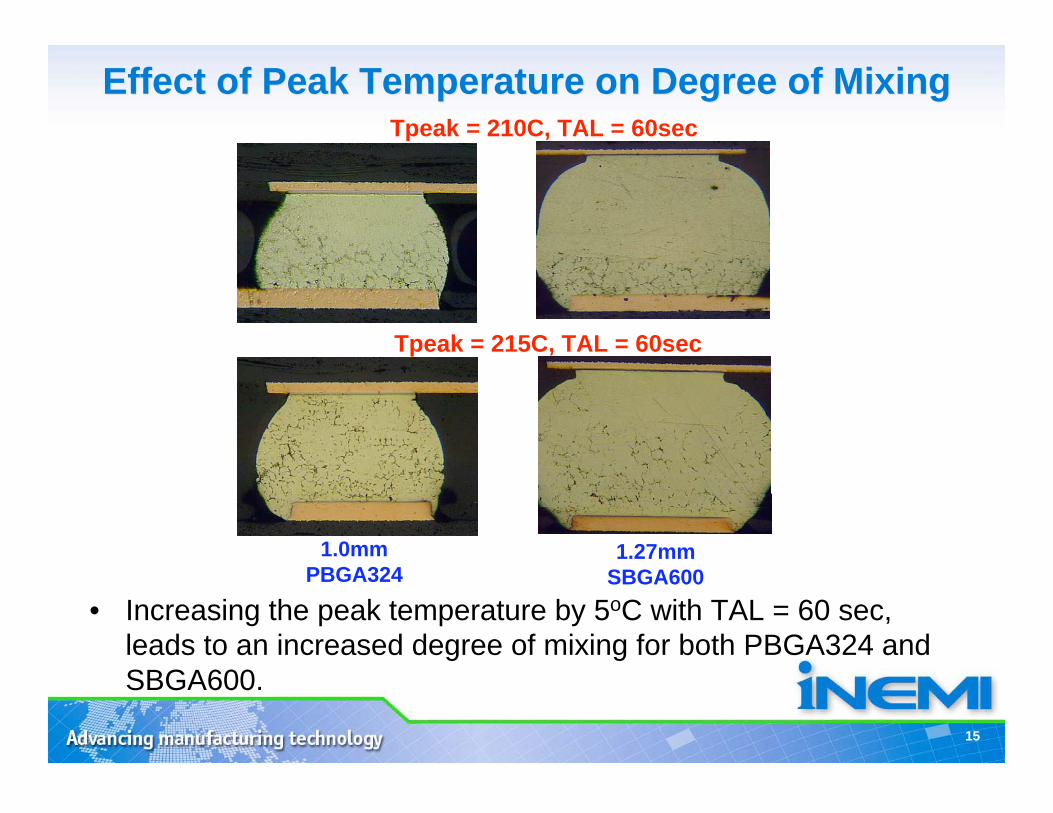
Effect of Peak Temperature on Degree of MixingEffect of Peak Temperature on Degree of MixingTpeak = 210C, TAL = 60sec
Tpeak = 215C, TAL = 60sec
• Increasing the peak temperature by 5oC with TAL = 60 sec,
leads to an increased degree of mixing for both PBGA324 and
SBGA600.
1.0mm
PBGA3241.27mm
SBGA600
16
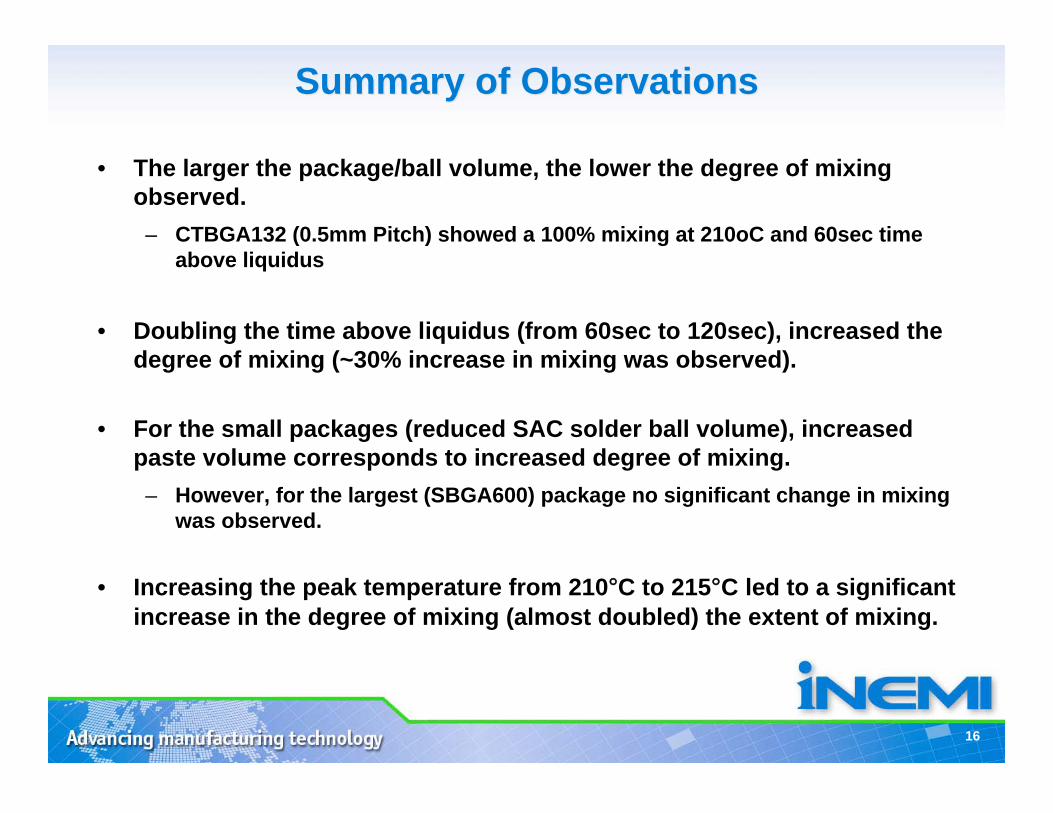
Summary of ObservationsSummary of Observations
• The larger the package/ball volume, the lower the degree of mixing
observed.
– CTBGA132 (0.5mm Pitch) showed a 100% mixing at 210oC and 60sec time
above liquidus
• Doubling the time above liquidus (from 60sec to 120sec), increased the
degree of mixing (~30% increase in mixing was observed).
• For the small packages (reduced SAC solder ball volume), increased
paste volume corresponds to increased degree of mixing.
– However, for the largest (SBGA600) package no significant change in mixing
was observed.
• Increasing the peak temperature from 210°C to 215°C led to a significant
increase in the degree of mixing (almost doubled) the extent of mixing.
17
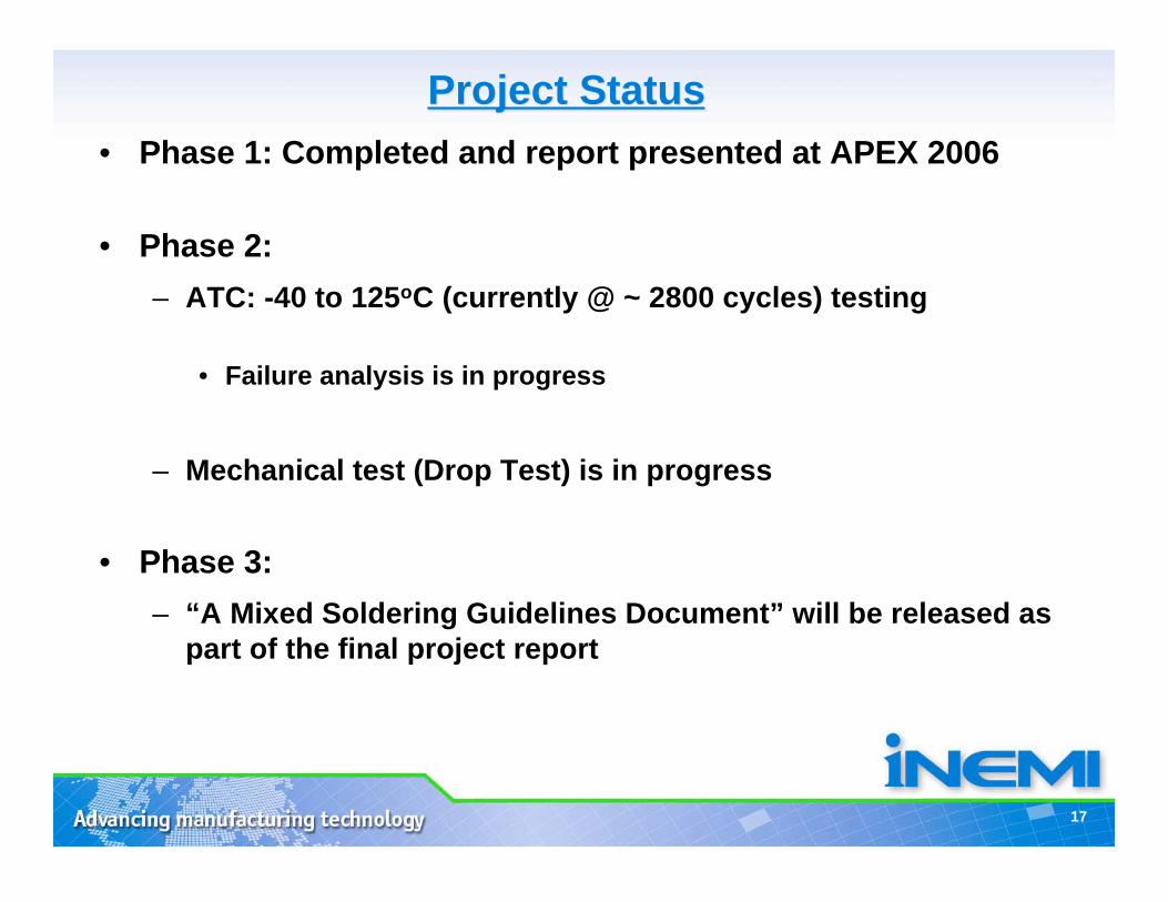
Project StatusProject Status
• Phase 1: Completed and report presented at APEX 2006
• Phase 2:
– ATC: -40 to 125oC (currently @ ~ 2800 cycles) testing
• Failure analysis is in progress
– Mechanical test (Drop Test) is in progress
• Phase 3:
– “A Mixed Soldering Guidelines Document” will be released as
part of the final project report
18
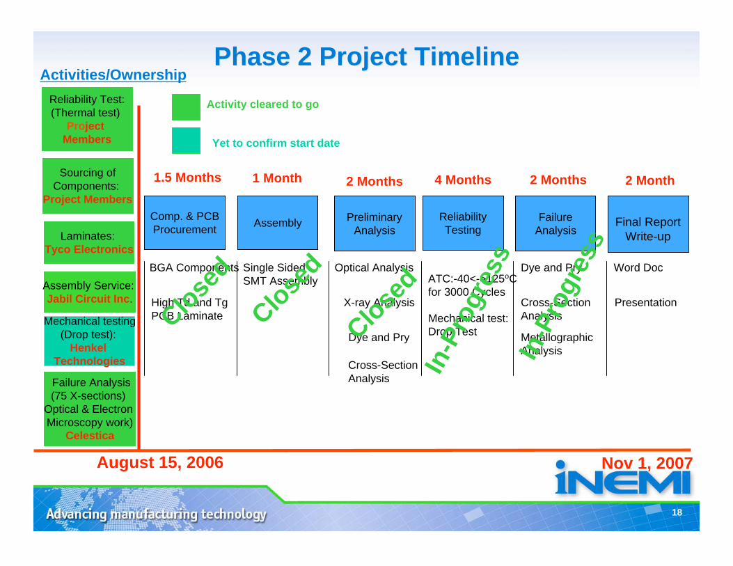
Phase 2 Project TimelinePhase 2 Project Timeline
Assembly Service:
Jabil Circuit Inc.
Reliability Test:
(Thermal test)
Project
Members
Sourcing of
Components:
Project Members
Failure Analysis
(75 X-sections)
Optical & Electron
Microscopy work)
Celestica
Comp. & PCB
ProcurementAssembly
Preliminary
Analysis
Reliability
TestingFailure
AnalysisFinal Report
Write-up
August 15, 2006
1.5 Months 1 Month 2 Months 4 Months 2 Months 2 Month
ATC:-40<->125oC
for 3000 Cycles
Mechanical test:
Drop Test
Cross-Section
Analysis
Dye and Pry
X-ray Analysis
Optical AnalysisSingle Sided
SMT Assembly
BGA Components
High Td and Tg
PCB Laminate
Cross-Section
Analysis
Dye and Pry
Metallographic
Analysis
Presentation
Word Doc
Nov 1, 2007
Laminates:
Tyco Electronics
Activities/Ownership
Activity cleared to go
Mechanical testing
(Drop test):
Henkel
Technologies
Clo
sed
Clo
sed
Clo
sed
In-P
rogre
ss
Yet to confirm start date
In-P
rogre
ss
19
Project ParticipantsProject Participants