patterned silver nanorod array substrates for surface-enhanced raman scattering
TRANSCRIPT

Patterned Silver Nanorod Array Substrates for Surface-EnhancedRaman Scattering
NICOLE E. MAROTTA, JABULANI R. BARBER, PETER R. DLUHY,and LAWRENCE A. BOTTOMLEY*School of Chemistry & Biochemistry, Georgia Institute of Technology, Atlanta, Georgia 30332-0400
A novel method for batch fabrication of substrates for surface-enhanced
Raman scattering (SERS) has been developed. A modified platen that fits
in a commercial electron beam evaporator enables the simultaneous
deposition of Ag nanorod arrays onto six microscope slides by glancing
angle deposition. Following removal of substrates from the evaporator,
patterned wells are formed by contact printing of a polymer onto the
surface. Well dimensions are defined by penetration of the polymer into
the nanorod array and subsequent photochemical curing. Inherent
advantages of this method include: (1) simultaneous production of several
nanorod array substrates with high structural uniformity, (2) physical
isolation of nanorod arrays from one another to minimize cross
contamination during sample loading, (3) dimensional compatibility of
the patterned array with existing SERS microscope, (4) large SERS
enhancement afforded by the nanorod array format, (5) small fluid
volumes, and (6) ease of use for manual delivery of fluids to each element
in the patterned array. In this article, the well-to-well, slide-to-slide, and
batch-to-batch variability in physical characteristics and SERS response
of substrates prepared via this method is critically examined.
Index Headings: Surface-enhanced Raman scattering; SERS; Surface-
enhanced Raman spectroscopy; Nanostructured silver surface; Micro-
contact printing; Glancing angle deposition; GLAD.
INTRODUCTION
Since its discovery in the mid-1970s,1–3 interest in surface-enhanced Raman scattering (SERS) has steadily grown.4–7 Ithas become a powerful analytical tool for determining analyteconcentration and characterizing the vibrational, rotational, andother low-frequency modes of molecules and molecularensembles.4,8–10 One impediment to its application in biologyis the difficulty involved in manufacturing SERS substrateswith reproducible performance characteristics.5,11,12 Recently,substrates comprising silver nanorod arrays have been shownto be highly uniform in structure, easy to fabricate, and providehigh signal enhancements.13–25 These substrates show promiseas solutions to the existing impediment to biosensor applica-tions.6,26–30
The nanorod arrays have been fabricated by glancing angledeposition (GLAD).19,20,31–39 GLAD is a physical vapordeposition technique that creates thin films consisting ofcolumnar microstructures as a result of atomic shadowing.40–42
The fabrication of SERS substrates with reproducible andreliable performance characteristics depends on precise controlof empirical parameters including flux angle, deposition rate,substrate temperature, etc.43 The angles used during GLADplay a crucial role in both the physical nature of themicrostructures and the porosity of the array.34,44,45 Densearrays are formed at low flux angles, whereas porous arrays areformed at flux angles greater than 808. For silver nanorod
arrays, a flux angle of 868 has been shown to be optimum forSERS applications.19–22,44–47 Variation in the levels of this andother empirical parameters negatively impacts the consistencyof the physical characteristics and SERS performance ofsubstrates fabricated by physical vapor deposition. One solutionto this problem is to prepare multiple substrates per batch and topattern each substrate, enabling multiple analyses per substrate.
We present herein an improved method for batch fabricationand patterning of SERS substrates. We have designed amodified platen for a commercial electron beam evaporator thatenables the simultaneous deposition of Ag nanorod arrays ontosix microscope slide substrates. Following removal of slidesfrom the evaporator, wells are patterned by contact printing of apolymer onto the nanorod array surface. Well dimensions aredefined by penetration of the polymer into the nanorod arrayand subsequent photocuring. Inherent advantages of thismethod include: (1) simultaneous production of severalnanorod array substrates with high structural uniformity, (2)physical isolation of nanorod arrays from one another tominimize cross contamination during sample loading, (3)dimensional compatibility of the patterned array with existingSERS microscopes, (4) large SERS enhancement afforded bythe nanorod array format, (5) small fluid volumes, and (6) easeof use for manual delivery of fluids to each element in thepatterned array. In this report, the well-to-well, slide-to-slide,and batch-to-batch variability in physical characteristics andSERS response are critically examined.
EXPERIMENTAL
Substrate Fabrication. The SERS substrates were fabricat-ed from standard 25 3 75 mm glass microscope slides. Theprocess began by immersing each slide in ‘‘piranha’’ solutionfor 30 min, copious rinsing with deionized water, and dryingunder a flowing nitrogen gas stream. Next, slides were placedin a CVC-601 DC Sputtering tool (Consolidated VacuumCorp., Rochester, NY) and thin films of titanium (50 nm)followed by silver (500 nm) were deposited onto one side ofthe slide normal to the surface. The titanium underlayerpromotes adhesion of the silver to the glass surface. Then, thesubstrates were positioned on the specially designed samplestage in the CVC-SC5000 electron beam evaporator (Consol-idated Vacuum Corp., Rochester, NY). Silver (99.99% fromKurt J. Lesker, Clairton, PA) was deposited onto the slides at adeposition rate of 3 A/s, a starting pressure of 1 3 10�6, and ata flux angle of 868 from normal until the apparent depositionthickness on the quartz crystal thickness monitor reached adeposition thickness reading of 1.5 lm. Since the monitor islocated closer to the source metal, this value is notrepresentative of nanorod length or average film thickness.The substrates were allowed to cool under vacuum for at least10 min prior to backfilling the chamber with nitrogen and
Received 19 June 2009; accepted 20 July 2009.* Author to whom correspondence should be sent. E-mail: [email protected].
Volume 63, Number 10, 2009 APPLIED SPECTROSCOPY 11010003-7028/09/6310-1101$2.00/0
� 2009 Society for Applied Spectroscopy
removal from the tool. Substrates were packaged in Uni-MailerTM slide holders (VWR Scientific Inc., West Chester,PA) and stored in a desiccator until use.
Substrate Patterning. Each slide was mounted in aspecially designed base with the nanorod array surface facingupward and in a fixed orientation with respect to nanorodgrowth direction. Next, a stamp comprising aluminum roundtubing (TTRA-05-12, Small Parts Inc, Miramar, FL) press-fitinto an aluminum plate was brought into contact with a thinfilm of ultraviolet (UV) curable epoxy (OG142, EPO-TEK,Billerica, MA) previously spread onto a clean microscopeslide. Then, the stamp was brought into momentary contactwith the Ag nanorod array with a vertical load sufficient totransfer the polymer to the Ag substrate. The pattern transferredto the substrate consisted of 36 rings and a solid circularmarking indicating nanorod growth direction. The slide wasremoved from the base and exposed to UV light for 10 min(UltraLum Model EA40 UV Transilluminator, Claremont, CA)to cure the polymer. Following patterning, slides were returnedto the holder and stored as above.
Substrate Characterization. Substrates were characterizedby scanning electron microscopy (SEM) and SERS. Scanningelectron micrographs were obtained using a Zeiss SEM Ultra60scanning electron microscope (Carl Zeiss SMT Inc., Peabody,MA). Images were acquired with an accelerating voltage of 5eV and at an incident angle of 528 relative to the surfacenormal. To minimize charging artifacts, slides were attached tothe holder using double-sided copper tape. Ion milling of theAg nanorod surface was performed using a FEI Nova NanoLab200 dual ion/electron beam microscope (FEI Corp., Hillsboro,OR). The substrate was imaged using the electron beam with a10 kV operating voltage and a beam current of 0.54 nA. Theion beam uses a Ga ion source with beam current of 30 pA andan operating voltage of 30 kV. To prevent beam-induceddamage of the surface, the ion beam was not used to image thesurface. Analysis of image features was performed usingSmartTiffTM, a software tool made available by Zeiss. SERSspectra were obtained with a Kaiser Optical Systems’ Holo-probe 785 spectrometer (Kaiser Optical Systems, Inc., AnnArbor, MI) using an excitation wavelength of 785 nm, a 103objective, an integration time of 10 s, and a surface power of4.5 mW. Rhodamine 6G (R6G) was used as the SERS probe.This analyte was used as received (Tokyo Kasei Kogyo Co.Ltd., Toshima, Japan). Stock solutions of 1.0 mM R6G wereprepared in deionized water and in sodium chloride, sodiumcitrate buffer (13 SSC, pH¼ 7.4). Test solutions were preparedby serial dilution of each stock. To characterize the SERSperformance of each substrate, 5.0 lL aliquots of the testsolution were applied to the desired well and allowed to dry ina desiccator. A minimum of five spectra were recorded per wellat random locations.
RESULTS AND DISCUSSION
In conventional GLAD fabrication, a single substrate ispositioned directly above the source material.48 This ensuresminimal variability in the flux angle37 and maximal metalplume density49–54 during evaporation from one batch toanother, assuming all other empirical parameters, includingsubstrate location, remain constant. When additional substratesare positioned above or below this one, the nanorod array oneach substrate will be of differing length and porosity.Substrates closer to the heated metal source will have longer
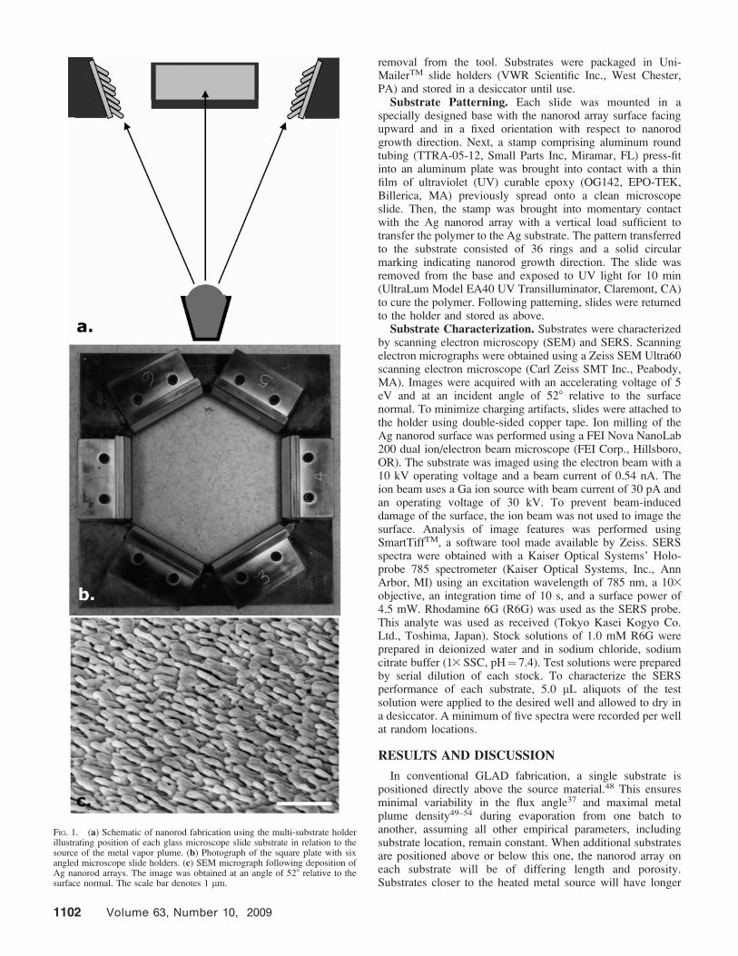
FIG. 1. (a) Schematic of nanorod fabrication using the multi-substrate holderillustrating position of each glass microscope slide substrate in relation to thesource of the metal vapor plume. (b) Photograph of the square plate with sixangled microscope slide holders. (c) SEM micrograph following deposition ofAg nanorod arrays. The image was obtained at an angle of 528 relative to thesurface normal. The scale bar denotes 1 lm.
1102 Volume 63, Number 10, 2009

nanorods; substrates further away from the heated metal sourcewill have shorter nanorods. The growth angle will also varywith distance since vertical stacking requires that eachsuccessive substrate be slightly offset from the one below toavoid shadowing effects.34 This offset changes the flux angleand atomic vapor density. In this context, we designed a holderthat places each substrate at the same distance and fixed anglefrom the source, thereby minimizing the metal vapor flux angleand density variability. This is shown schematically in Fig. 1a.
A custom multi-substrate stage was designed specifically foruse in a CVC electron beam evaporator; a photograph of thestage is presented in Fig. 1b.� The stage consists of a circularaluminum platen with four aluminum rod stand-offs machinedto enable rapid and reliable placement into the multi-userevaporator. A square opening (17.0 cm per side) was cut intothe platen to allow the metal plume to pass. Because thespecific tool is equipped with multiple crucibles that can berotated into position during an evaporation, the center of thesquare was located above the source position rather than at thecenter of the platen. A hexagonal opening was cut into thecenter of a square aluminum plate with two aluminumpositioning pegs extending below the plate for ease ofplacement into the opening of the circular standoff plate. Tothe square plate, six angled slide holders were mounted flushwith the edge of the hexagonal opening and held rigidly inplace by two screws. Standard 25 3 75 mm glass microscopeslides were mounted onto each holder by placement of the longedge of the slide onto a 1.0 mm deep ledge that was cut intoeach holder; double-sided adhesive tape ensured that the slidewould not move during transfer or metal deposition. The centerof each slide was rigidly held at a horizontal distance of 8.5 cmand a vertical distance of 42.1 cm from the source and at afixed angle of 80.98. This angle provides a flux angle of 868during metal deposition.�
A SEM micrograph of the Ag nanorod array is presented inFig. 1c and is typical of those obtained for all six substrates.Images acquired in this fashion illustrate the consistency ofnanorod thickness and spatial distribution; measurement ofnanorod growth angle and length required FIB milling of aportion of the array to enable edge-on viewing. Analysis ofimages acquired following FIB milling of each substrateindicated that a consistent growth angle of 57 6 0.58 and a fluxangle of 86 6 0.58 were achieved with our custom slide holder.Nanorod lengths were 450 6 15 nm across a single slide, 4506 20 nm across a batch, and 450 6 15 nm between substratesfrom different batches.
To maximize the number of samples that can be analyzed persubstrate, polymer wells were patterned onto the substratesthrough contact printing using the stamp depicted in Fig. 2a.The stamp assembly consists of a slide holder and stamp. Arectangular slot was cut into an aluminum plate to rigidly holdthe slide in fixed position during stamping. Four guidepostswere attached to the corners of the holder plate; compressionsprings were placed onto these guideposts to mediate thepressure applied to the substrate during stamping. The stamp
consisted of thirty-six aluminum tubes (0.18 mm outerdiameter) positioned in three rows of twelve with 1 mmspacing, which were press-fit into a second aluminum plate. Tomark the growth orientation of the nanorods, a closed-endaluminum rod was press-fit into the aluminum plate adjacent toone of the tubes. In Fig. 2a, this rod is located below the tubeon the lower right side of the stamp.
Circular wells were patterned onto the slide by momentarycontact of the stamp, pre-loaded with UV curable epoxy, ontothe nanorod array. This particular epoxy was chosen because:(1) walls can be created in a single application, (2) it has anindefinite handling time, (3) there is no out-gassing duringcuring, and (4) UV exposure did not diminish the SERSperformance of the nanorods (see below). Figure 2b shows aphotograph of a patterned substrate. Each well holds up to 20lL of sample solution. Note: the number of wells per substratecan be readily increased and the volume of sample reduced byusing tubing of smaller diameter.§
FIG. 2. (a) Photograph of the stamp assembly used for patterning substrates;(b) photograph of a patterned Ag nanorod substrate.
� Photographs of individual components are included in the SupplementaryMaterial.
� In an earlier prototype, individual plate holders for the stage consisted of aspring-tensioned hinged platform. A positioning screw acting against thespring tension allowed for control of the deposition angle. Each holder iscapable of suspending the substrates at a GLAD angle between 08 and 908.Photographs of this prototype are also included in the SupplementaryMaterial.
§ In our experience, a gap between each circular barrier is needed to preventwicking of solutions in adjacent wells.
APPLIED SPECTROSCOPY 1103

The SERS performance of each substrate was determinedusing R6G. A 5 lL aliquot of an aqueous solution of R6G(10�5 M), with or without buffer, was placed into the wells andallowed to evaporate. Figure 3 presents a spectrum typical of
those obtained for aqueous solutions without buffer.55–57 Thespectrum contains all the spectral bands expected for thismolecule. A surface enhancement factor58 of 1 3 107 wascomputed for the 1360 cm�1 band relative to the bulk sample.This value falls within the range previously reported forsubstrates produced by glancing angle deposition.22 Spectraobtained when R6G was dissolved in 13 SSC also containthese lines as well as spectral bands associated with sodiumchloride and sodium citrate (SSC) buffer (data not shown).
Figures 4a and 4c present photographs of two adjacent wellsfrom the same slide following evaporation of 50 picomoles ofR6G dissolved in water and in 13 SSC buffer, respectively. InFig. 4a, the dotted line designates the area covered by analyte.In Fig. 4c, the entire area of the well is covered by analyte,suggesting that the presence of salt in the sample solutiondramatically increases the wettability of the Ag nanorodsurface.
Spectra were acquired across each well in 25 lm steps, alongthe dashed line in the figure. The background-corrected peakintensities obtained as a function of position are plotted in Figs.4b and 4d for the aqueous and buffered R6G solution,respectively. The span of the x-axis in both plots encompassesthe diameter of each well. There is minimal variability in peakintensity of all four spectral bands across the well whereanalyte was deposited from water solution (Fig. 4b). This data
FIG. 3. SERS spectrum obtained on 50 picomoles of R6G deposited into awell. Both the raw and background-corrected (BC) spectra are displayed. Peakslabeled with an asterisk designate the spectral lines used in comparing SERSperformance from well to well, slide to slide, and batch to batch.
FIG. 4. Optical images of a well on the patterned SERS substrate following evaporation of 5.0 lL aliquots of R6G in (a) water and (c) 13 SSC buffer. SERS spectrawere acquired in 25 lm step increments along the central dashed line. SERS peak intensities for the spectral lines of R6G noted in Fig. 3 are plotted as a function ofposition across the well in (b) water and (d) 13 SSC buffer. The thin dashed line represents the evaporation spot for R6G in water. Note that the substrate used forthis data had nanorods that were 900 6 25 nm in length.
1104 Volume 63, Number 10, 2009

suggests that there is uniformity in both analyte concentrationand SERS enhancement within the array.59 In contrast, spectraacquired across the well containing buffered R6G displaypeaks of lower intensity and greater variability (Fig. 4d). Thereduced intensity is presumably due to the increased spatialdistribution of analyte across the well resulting in a decrease inthe number of analyte molecules within the laser spot. Theincreased variability in signal intensity as a function of positionis most likely a result of spectral interference from salt crystaldeposits on top of and within the Ag nanorod array (Fig. 4c).Based on this finding, comparison of the SERS performancefrom well to well, substrate to substrate, and batch to batch wasassessed using an unbuffered solution of R6G.
Figure 5 compares the peak intensities for R6G acquired as afunction of well number, substrate number, and batch number.Each data point is the average intensity of at least five spectraacquired at different locations within the well. The error bardenotes the standard deviation from the average value. It hasbeen previously shown that the magnitude of SERS enhance-ment depends upon nanorod length.22 The length of thenanorod depends upon the plume density and duration of metaldeposition. As a result of the design characteristics of oursubstrate holder, the sides of each slide are located at a distanceof 0.17 cm farther from the source than the middle of the slide.Similarly, the top of each slide is located at a distance of 3.37cm farther from the source than the bottom of the slide.
Figure 5a presents a plot of peak intensity as a function ofwell number across a row of wells on a single substrate.Minimal variation in SERS peak intensity is observed acrossthe row, suggesting nominal changes in nanorod length, a factsupported by SEM characterization. Figure 5b presents a plotof peak intensity as a function of well number down a columnof wells on the same substrate. The variance in SERS peakintensity is greater than across the well. The curvilinear trendsuggests that SERS enhancement is a function of both nanorodlength and growth angle.
Figure 5c presents a plot of peak intensity for the 771 cm�1
band acquired on specific wells across a row as a function ofslide position within a given batch. A small amount ofvariability is observed from one substrate to another andreflects differences in the plume density from slide to slide.Because of our efforts to hold each slide at an exact distancefrom the source, we attribute this difference in plume density tothe random and uncontrollable movement of the electrical arcon the ingot during deposition. This effect may be minimizedby rotation of the platen during deposition, a feature outside thecapability of our evaporator. Figure 5d presents a plot of peakintensity for the 771 cm�1 band acquired on specific wellsacross a row on slide #1 as a function of batch. Theperformance repeatability from batch to batch is a factor oftwo better than that previously reported.22
CONCLUSION
Multiple nanorod array substrates may be fabricated in aconventional electron beam evaporator by judicious placementof each substrate within the metal vapor plume. Careful controlof evaporation parameters results in high uniformity of nanorodmorphology and SERS performance characteristics from onebatch to another. Patterning of the substrate following nanoroddeposition increases the number of assays that can beperformed from a single batch. Variability in SERS perfor-mance was 6% (relative standard deviation in intensity) across
FIG. 5. Plot of peak intensities for the bands identified in Fig. 3 as a functionof well number (a) across a row and (b) down a column for the same substrate.A plot of peak intensity for the 771 cm�1 band as a function of well numberacross a row for (c) all six substrates fabricated in the same batch and (d) fromtwo different batches.
APPLIED SPECTROSCOPY 1105
a substrate, 25% down a substrate, 15% from one substrate toanother within a batch, and only 8% from batch to batch. Notethat these variations were determined from background-corrected spectral intensities without normalization. Currenteffort is focused on developing SERS based bioassays usingthese Ag nanorod array substrates.
ACKNOWLEDGMENTS
We thank Prof. Mohan Srinivasarao for allowing our extended use of hisRaman spectrometer, Dr. Matija Crne for his help in keeping this spectrometerin working order, Charlie Suh for suggestions on the design of the multiplesubstrate platen, Katherine Siemens for assistance in processing Raman spectraldata, and Kane Barker for ion milling the nanorod arrays. We acknowledgefruitful discussions with Profs. R. A. Dluhy, R. A. Tripp, and Y. Zhao of theUniversity of Georgia on the fabrication and characterization of substrates.Financial support of this research through grants from the Georgia Tech/UGABiomedical Research program and the Georgia Research Alliance VentureLabprogram is gratefully acknowledged.
SUPPLEMENTAL MATERIAL
All supplemental material mentioned in the text is availableon line at http://www.s-a-s.org.
1. M. G. Albrecht and J. A. Creighton, J. Am. Chem. Soc. 99, 5215 (1977).2. M. Fleischmann and P. J. Hendra, A. J. McQuilla. Chem. Phys. Lett. 26,
163 (1974).3. D. L. Jeanmaire and R. P. Vanduyne, J. Electroanal. Chem. 84, 1 (1977).4. R. Aroca, Surface Enhanced Vibrational Spectroscopy (John Wiley and
Sons, New York, 2006).5. K. A. Willets and R. P. Van Duyne, Annu. Rev. Phys. Chem. 58, 267
(2007).6. J. P. Scaffidi, M. K. Gregas, V. Seewaldt, and T. Vo-Dinh, Anal. Bioanal.
Chem. 393, 1135 (2009).7. T. Vo-Dinh, F. Yan, and M. B. Wabuyele, Top. Appl. Phys. 103, 409
(2006).8. M. Moskovits, Rev. Modern Phys. 57, 783 (1985).9. R. L. McCreery, Raman Spectroscopy for Chemical Analysis (Academic
Press, New York, 2000).10. K. Kneipp, Phys. Today 60, 40 (2007).11. P. L. Stiles, J. A. Dieringer, N. C. Shah, and R. P. Van Duyne, Annu. Rev.
Anal. Chem. 1, 601 (2008).12. S. Lal, N. K. Grady, J. Kundu, C. S. Levin, J. B. Lassiter, and N. J. Halas,
Chem. Soc. Rev. 37, 898 (2008).13. C. L. Leverette, V. A. Shubert, T. L. Wade, K. Varazo, and R. A. Dluhy, J.
Phys. Chem. B 106, 8747 (2002).14. C. L. Leverette and R. A. Dluhy, Colloids Surf. A 243, 157 (2004).15. S. B. Chaney, S. Shanmukh, R. A. Dluhy, and Y. P. Zhao, Appl. Phys.
Lett. 87, 031908/1 (2005).16. C. L. Leverette, S. A. Jacobs, S. Shanmukh, S. B. Chaney, R. A. Dluhy,
and Y. P. Zhao, Appl. Spectrosc. 60, 906 (2006).17. Y. Liu, J. Fan, Y. P. Zhao, S. Shanmukh, and R. A. Dluhy, Appl. Phys.
Lett. 89, 173134/1 (2006).18. S. Shanmukh, L. Jones, J. Driskell, Y. P. Zhao, R. Dluhy, and R. A. Tripp,
Nano Lett. 6, 2630 (2006).19. Y. P. Zhao, S. B. Chaney, S. Shanmukh, and R. A. Dluhy, J. Phys. Chem.
B 110, 3153 (2006).20. Y. P. Zhao, S. H. Li, S. B. Chaney, S. Shanmukh, J. G. Fan, R. A. Dluhy,
and W. Kisaalita, J. Electron. Mater. 35, 846 (2006).21. Y. P. Zhao, S. Shanmukh, Y. J. Liu, S. B. Chaney, L. Jones, R. A. Dluhy,
and R. A. Tripp, Proc. SPIE-Int. Soc. Opt. Eng. 6324, 63240M/1 (2006).
22. J. D. Driskell, S. Shanmukh, Y. Liu, S. B. Chaney, X. J. Tang, Y. P. Zhao,and R. A. Dluhy, J. Phys. Chem. C 112, 895 (2008).
23. J. D. Driskell, S. Shanmukh, Y.-J. Liu, S. Hennigan, L. Jones, Y.-P. Zhao,R. A. Dluhy, D. C. Krause, and R. A. Tripp, IEEE Sens. J. 8, 863 (2008).
24. S. Shanmukh, L. Jones, Y.-P. Zhao, J. D. Driskell, R. A. Tripp, and R. A.Dluhy, Anal. Bioanal. Chem. 390, 1551 (2008).
25. R. A. Tripp, R. Dluhy, and Y.-P. Zhao, NanoToday 8, 31 (2008).26. A. Dhawan, Y. Zhang, F. Yan, M. Gerhold, and T. Vo-Dinh, Proc. SPIE-
Int. Soc. Opt. Eng. 6869, 68690G/1 (2008).27. T. Vo-Dinh, IEEE J. Sel. Top. Quantum Electron. 14, 198 (2008).28. J. N. Anker, W. P. Hall, O. Lyandres, N. C. Shah, J. Zhao, and R. P. Van
Duyne, Nat. Mater. 7, 442 (2008).29. X. M. Qian and S. M. Nie, Chem. Soc. Rev. 37, 912 (2008).30. A. Barhoumi, D. Zhang, F. Tam, and N. J. Halas, J. Am. Chem. Soc. 130,
5523 (2008).31. M. J. Brett, M. W. Seto, J. C. Sit, K. D. Harris, D. Vick, and K. Robbie,
Proc. SPIE-Int. Soc. Opt. Eng. 3790, 114 (1999).32. K. Robbie and M. J. Brett, J. Vac. Sci. Technol., A 15, 1460 (1997).33. K. Robbie, C. Shafai, and M. J. Brett, J. Mater. Res. 14, 3158 (1999).34. K. Robbie, J. C. Sit, and M. J. Brett, J. Vac. Sci. Technol., B 16, 1115
(1998).35. J. P. Singh, T. Karabacak, D. X. Ye, D. L. Liu, C. Picu, T. M. Lu, and G.
C. Wang, J. Vac. Sci. Technol., B 23, 2114 (2005).36. J. C. Sit, D. Vick, K. Robbie, and M. J. Brett, J. Mater. Res. 14, 1197
(1999).37. R. N. Tait, T. Smy, and M. J. Brett, Thin Solid Films 226, 196 (1993).38. Y. P. Zhao, S. B. Chaney, and Z. Y. Zhang, J. Appl. Phys. 100, 063527/1
(2006).39. Y. P. Zhao, D. X. Ye, G. C. Wang, and T. M. Lu, Nano Lett. 2, 351 (2002).40. L. Abelmann and C. Lodder, Thin Solid Films 305, 1 (1997).41. A. Amassian, K. Kaminska, M. Suzuki, L. Martinu, and K. Robbie, Appl.
Phys. Lett. 91, 173114/1 (2007).42. H. Vankranenburg and C. Lodder, Mater. Sci. Eng. R-Reports 11, 295
(1994).43. L. W. Bezuidenhout and M. J. Brett, Mater. Res. Soc. Symp. Proc. 0951-
E11-06 (2007).44. M. O. Jensen and M. J. Brett, J. Nanosci. Nanotechnol. 5, 723 (2005).45. M. O. Jensen and M. J. Brett, Appl. Phys. A: Mater. Sci. Process. 80, 763
(2005).46. M. M. Hawkeye and M. J. Brett, J. Vac. Sci. Technol., A 25, 1317 (2007).47. J. J. Steele and M. J. Brett, J. Mater. Sci.: Mater. Electron. 18, 367 (2007).48. M. J. Brett and M. M. Hawkeye, Science (Washington, D.C.) 319, 1192
(2008).49. J. Balakrishnan, I. D. Boyd, and D. G. Braun, J. Vac. Sci. Technol., A 18,
907 (2000).50. O. Ellegaard, J. Schou, and H. M. Urbassek, Appl. Phys. A: Mater. Sci.
Process. 69, S577 (1999).51. J. Fan, I. D. Boyd, and C. Shelton, J. Vac. Sci. Technol., A 18, 2937
(2000).52. H. W. Liu, M. R. Wang, J. K. Wang, G. Y. Zhang, H. L. Liao, R. Huang,
and X. Zhang, Appl. Thermal Eng. 27, 323 (2007).53. P. Minson, A. Powell, and G. Trapaga, Proceedings of the Conference on
Electron Beam Melting and Refining-State of the Art 1996, 126 (1996).54. A. Powell, P. Minson, G. Trapaga, and U. Pal, Metal. Mater. Trans. A-
Phys. Metal. Mater. Sci. 32, 1959 (2001).55. Y. C. Liu, C. C. Yu, and S. F. Sheu, J. Mater. Chem. 16, 3546 (2006).56. D. Pristinski, S. L. Tan, M. Erol, H. Du, and S. Sukhishvili, J. Raman
Spectrosc. 37, 762 (2006).57. J. A. Dieringer, K. L. Wustholz, D. J. Masiello, J. P. Camden, S. L.
Kleinman, G. C. Schatz, and R. P. Van Duyne, J. Am. Chem. Soc. 131,849 (2009).
58. E. C. Le Ru, E. Blackie, and P. G. Etchegoin, J. Phys. Chem. C 111, 13794(2007).
59. J. P. Camden, J. A. Dieringer, Y. Wang, D. J. Masiello, L. D. Marks, G. C.Schatz, and R. P. Van Duyne, J. Am. Chem. Soc. 130, 12616 (2008).
1106 Volume 63, Number 10, 2009