part v - springer978-1-4615-5267-3/1.pdf · n-diff-p-well 0.47 2.25 2.22 x 10"" 1 x 10~u...
TRANSCRIPT

Part V Appendices

Appendix A
Quantum Efficiency of Photodetectors
Each of the photodetector structures illustrated in Figure 5.1 can be analyzed relatively easily. Here we provide an analysis for each device, and derive equations for the quantum efficiency as a function of the geometrical and metallurgical parameters of the devices. The simplifying assumptions made in all derivations in the following sections are:
• Abrupt junctions with rectangular depletion regions.
• One dimensional current flow. This would not be true for minimum size devices, where vertical and horizontal dimensions are comparable.
• No high-level injection. This becomes important for very high intensity applications, for example for furnaces or welding inspection.
• No degeneration in highly doped diffusion regions.
• No recombination in depletion regions.
• No surface recombination. This parameter is particularly important for lateral devices and for photo gates, where there is a significant number of active carriers close to the surface. In vertical devices, the processes which determine the characteristics of the device depend mainly on the parameters of bulk semiconductor.
• No surface reflectance.
• No diffusion in the bulk substrate. This is important for near infra-red detectors, as most of the carrier generation happens close to the bulk substrate.
There are also some other assumptions made for each device which will be explained individually when treating each device.

Appendix A. Quantum Efficiency of Photodetectors
In order to improve the consistency between the simulation results from the derived equations and real measured data, the above parameters should be taken into account. However, the derived equations can still provide a good insight into the device operation, and illustrate the effect of different parameters on the quantum efficiency. Moreover, there are no accurate data available for the physical and metallurgical parameters in most processes, and hence these will be ignored here. In the extreme case one can use device simulation software to numerically derive the device characteristics.
A.1 Quantum Efficiency of a Vertical Junction Diode
For the structure shown in Figure A.I, the photocurrent is composed of two components: the drift current due to the drift of holes and electrons in the depletion region, and the diffusion current due to the diffusion of carriers outside the depletion region.
P-well Xj
Xepi
Figure A.I: The structure of a junction photodetector. Xi is the metallurgical junction depth, W is the width of the depletion region, and xepi is the thickness of the epitaxial layer.
The drift current in the depletion region is:
l ",j+",,,
Jdrift = -q G(x)dx "'j-"'p
(A. I)
246

Vision Chips Part V. Appendix
where G{x) is the carrier generation rate for an incident photon flux, 1).)0, in a semiconductor with an absorption coefficient of a, and is given by
(A.2)
Hence
1. ;J. -a{x· -x )(1 -aW) drift = q~oe 3 p - e (A.3)
xn and xp are the extent of the depletion region in the nand p sides of the junction and are given by
xn = (A.4)
xp =
where Vr is the reverse bias voltage applied to the junction, and Vo is the built-in potential of the junction, and is given by
Vo = kT In NAND q n~
(A.S)
The diffusion component of the current can be found from the diffusion equation:
D a2pr - Pn - PnO + G{x) = 0 in the N-substrate Pax Tp
(A.6)
where Dn and Dp are the diffusion coefficients of the minority carriers, Tp and Tn are the lifetime of excess carriers, and PnO and npO are the eqUilibrium minority carrier densities. The above equation can be solved under the boundary conditions Pnl"="ePi = 0, Pnl.,=.,;+., .. = 0, npl.,=o = npO, and npl.,=.,;_.,p = 0 to obtain
Pn{x) = PnO + Aei; + Be -i; + Ce-ax (A.7)
247

Appendix A. Quantum Efflciency of Photodetectors
where Lp and Ln are the diffusion lengths of excess carriers, and
( (x· - x »)
D ~ F e-a ("; - ",1- e - 'Ln' +n"o
2 . h (Xj - xp) - sm Ln
The diffusion current can be expressed as:
248
(A.8)

Vision Chips Part V. Appendix
which can be simplified as:
!2:£. 1 - coshKp !2:£. e-O:Xepi q Ln PnO sinhK + q Ln C sinhK p p p p
CD -o:(x, + xn) ( _ COShKk ) +q pe J 0: Lpsinh p
!2:n. 1 - cosh K n + !2:n. F 1 +q Ln npO sinh Kn q Ln sinh K -qFDne-O:(Xj - xn) (0: + co~hK:k '\
Ln smh .,;) (AIO)
The parameters Dn , Dp , Tn, and Tp can be derived from the following empirical formulas for silicon, as a function of impurity densities
r. - 1 p - 7.8 x 10 13 N D + 1.8 x 10 '&1 Nb
_ kT ( 370) Dp - q 370 + 1 + 1.563 x 10 IS N D
r. - 1 n - 3.45 x 10 12 N A + 9.5 x 10 32 N1
Dn= k[ (232+ 1+1.12~~~0 17NA)
(All)
The total current Jopt is the sum of the drift and diffusion currents.
J opt = Jdri/t + Jdi/ / (AI2)
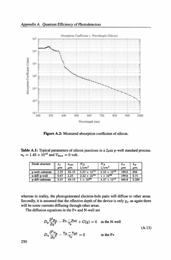
The above equations may be simplified for single-sided and shallow junctions to provide a better understanding of the effect of different parameters on the photoresponse of the device, but we keep them in their general form. The measured absorption coefficients for silicon are shown in Figure A.2. Typical parameters of a powell-substrate and a diffusion-well silicon junctions are shown in Table AI. The simulated quantum efficiency, Jopt!iJ!o, for these devices is plotted in Figure A.3. The quantum efficiency of the diffusion-substrate junction is higher than the other two structures, and also spans over a wider spectrum.
A.2 Quantum Efficiency of a Lateral Junction Diode
The structure of a lateral photodiode is shown in Figure AA. For analysis purposes, a few simplifying assumptions are made. Firstly, only the area between the two diffusion regions is assumed to be exposed to light. Otherwise, there will be a large contribution from the vertical bipolar component formed by p-diffusionln-weIVp-substrate,
249
Appendix A. Quantum Efficiency of Photodetectors
Absorption Coefficient v. Wavelength (Silicon) 10)~----r-----~----'-----~----~-----r----~----~
102 ::t·, :;" ..
E -< 101 '. ~,
c: <> '0 to:: .....
100 2:1 (,) c 0
'':: e- 10.1 :il
.&> «
10.2
10') 200 300 400 500 600 700 800 900 1000
Wavelength (run)
Figure A.2: Measured absorption coefficient of silicon.
Table A.1: Typical parameters of silicon junctions in a 2JLm p-well standard process. ni = 1.45 x 10¹⁰ and Vbias = 0 volt.
Diode structure Xj Xepi ND NA Ln Lp p.m p.m 1/cm3 1/cm3 p.m p.m
p-well-substrate 2.25 10-15 5.07 x 10'" 2.22 X 10"" 199.6 694 n-diff-p-well 0.47 2.25 2.22 x 10"" 1 x 10~u 199.6 0.71 p-diff-substrate 0.47 10-15 1 x lO~u 4.37 x 10"0 446.8 0.289
whereas in reality, the photogenerated electron-hole pairs will diffuse to other areas. Secondly, it is assumed that the effective depth of the device is only Yj, as again there will be some currents diffusing through other areas.
The diffusion equations in the P+ and N-well are
D a2P2n - Pn - PnO + G{y) = 0 in the N-well Pax Tp
(A. 13)
in the P+
250

Vision Chips Part Y. Appendix
0.9
Diff-Well 0.8 , - -'- Diff-8ub
"- Well-8ub / , , ,
0.7 , \
.",. "- , 0.6 I ,
'; \
I" I 0.5 ,.
,.' II ,
0.4 r , i
, \
I \ ~
0.3 \
I \
! \
\ 0.2 "-
"- , " 0.1
_.-=:&.1 0 200 300 400 500 600 700 600 900 1000 1100
Figure A.3: Simulated quantum efficiency versus wavelength for three differentjunction diodes in a 2Jtm process.
By taking into account the boundaryconditionsPnlz~z; = 0 and Pn Iz=z" = O. we will have
(A. 14)
251

Appendix A. Quantum Efflciency of Photodetectors
The drift current is simply
hri/t = -q~oG(y)(xn + xp) ~ -q~OG(y)xn (A. 15)
The total current can be obtained by integrating the addition of the drift and diffusion components across the depth and width of the device.
Jtotal = loy; [A-(B+qxn)~oG(Y)ldy = AYj+(B+qxn)~o{e-ayj -I} (A.16)
where
(A. 17)
(A.18)
Figure A.5 shows the simulation result of this structure for a typical 2pm process. As expected, there is a large blue response because all the carriers generated close to the surface are absorbed by the device. The poor response at longer wavelengths is due to the fact that we have considered the contribution of those carriers which are up to y - j deep into the device, which is very shallow. This structure can be combined with the vertical photodiode, by exposing all sides of the diode to light.
A.3 Quantum Efficiency of a Vertical Bipolar transistor
The structure of a vertical bipolar transistor is shown in Figure A.6. It is assumed that only the flat area is exposed to light, as otherwise, there will be some contribution from the vertical walls of the emitter-base and base-collector junctions.
We can write the diffusion equation in the three regions as:
Dne a:n~e _ npe; npeO + G(x) = 0 in the P-Emitter '1x ne
D b a P~b - Pnb - PnbO + G(X) = 0 in the N-Base (A.19) p ~x 'Tpb
D a n~c _ npc - npco + G(x) = 0 in the P-Collector nc ax 'Tnc
252

Vision Chips Part Y. Appendix
Yj
Figure A.4: The structure of a lateral junction diode in an N-Well CMOS process.
The boundary conditions are:
in emitter
in base (A.20)
253

Appendix A. Quantum Efficiency of Photodetectors
0.7.-----.-------.-------.------.-------.-----.
0.6
0.5
0.4
0.3
0.2
0.1
Dill-Well Diff-Sub Well-Sub
oL-______ L-______ L-______ L-______ L-==~~~ ____ ~
o 200 400 600 800 1000 1200
Figure A.5: Simulation result of the lateral photodiode in a 2JLm CMOS process.
The diffusion equations can be solved as follows.
npe(x) = npeO + Aet + Be -t + Ce-ax x X
Pnb(X) = PnbO + Eer,; + Fe -r,; + He-ax (A.21)
npc(x) = npco + Ket + Me -t + Re-ax
(A22)
(A23)
(A24)
254

Vision Chips Part V. Appendix
Xje
Figure A.6: The structure of a vertical bipolar detector in an N-Well CMOS process.
(A.25)
F = p,.bo(e+Y (e W -1 +2e+X )_H(e-Q(-;.+z,..le+Y _e-Q(z;c-a,.cl e+x e e
(A.26)
and
X - Xje +Xne - Lb
Y _ Xjc -Xnc - Lb (A.27)
255

Appendix A. Quantum Efficiency of Photodetectors
U - Xjc + xpc - Lc (A.30)
The diffusion component of the emitter and collector currents can be expressed as:
J . - - D an~e(X) I D apll(x) I dtff,E - q e X X=Xje-Xpe + q b X X=Xje+Xne
Jdiff,e = -qDc an~~x) IX=Xje+xpe + qDb apa~x) IX=Xjc-Zne
(A.31)
The drift components can be simply obtained_by integrating the amount of generated electron-hole pairs in the depletion regions.
Jdrift = Jdepletion -qG(x)dx Jdrift,E = _q(>o(e-O:(Xje + xne) _ e-O:(Xje - Xpe)) (A.32)
Jdrift,e = +q(>o(e-O:(XjC + xpc) _ e-O:(Xjc - Xnc))
As the base of this device is floating, the collector and emitter currents should be equal. The only variable parameter, which is unknown, is VEB. The value of VEB
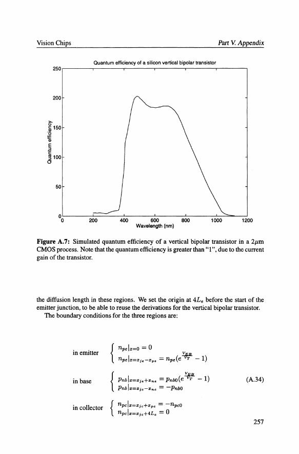
for which Ie = IE can be found using numerical methods. Figure A.7 shows the quantum efficiency of a typical parasitic PNP transistor in a 2p.m process. The large gain is simply due to the current gain of the bipolar transistor, which is larger than one. As expected the response is relatively flat over the visible spectrum, which is due to the presence of two junctions at two different depths in the device.
A.4 Quantum Efficiency of a Lateral Bipolar Photodetector
The structure of a lateral bipolar device is shown in Figure A.8. The simplifying assumptions are similar to those made in Section A.2, except that exposure to light is assumed to be only in the area between the emitter and collector diffusions, and the depletion regions.
Note that in Equation A.33, x denotes the horizontal axis and y the vertical axis. Also yjis the depth of the collector/emitter junctions.
The diffusion equations in the three regions can be written as:
D a2n~e _ npe - npeO = 0 ne ax Tne in P-Emitter
D a2p~b _ pnb - pnbO + G(y) = 0 in N-Base pb ax Tpb
(A.33)
in P-Collector
The diffusion length in the collector and emitter regions is very short. Therefore, we make another simplifying assumption, in that these junctions extend to four times
256
Vision Chips Part V. Appendix
Quantum efficiency of a silicon vertical bipolar transistor 250r-------r-------,-------,-------,-------,-------,
200
~ Iii 150 'u :; E :> C ~ 100 o
50
OL-------~------~------~--------~------~~~---J o 200 400 600 800 1000 1200 Wavelength (nm)
Figure A.7: Simulated quantum efficiency of a vertical bipolar transistor in a 2pm CMOS process. Note that the quantum efficiency is greater than "1", due to the current gain of the transistor.
the diffusion length in these regions. We set the origin at 4Le before the start of the emitter junction, to be able to reuse the derivations for the vertical bipolar transistor.
The boundary conditions for the three regions are:
in emitter { npelx=o = 0 - ~ npelx=Xie-Xpe -npe(e T -1)
{ ~
in base Pnblx=Xie+Xne = PnbO(e VT - 1) (A. 34) Pnblx=Xic-Xnc = -PnbO
in collector { npCIX=Xic+Xpc = -npco
npCIX=Xic+4Lc = 0 257

Appendix A. Quantum Efficiency of Photodetectors
Yj
Figure A.S: The structure of a lateral bipolar detector in an N-Well CMOS process.
By solving the equation we have.
t: -t: npe(x) = npeO + Ae e + Be e
Pnb(X) = PnbO + G(y)Tb + Eeib + Fe-ib (A.35)
t; -t; npc(x) = npco + Ke c + Me c
(A.36)
(A.37)
258

Vision Chips Part V. Appendix
Z _ Xje - Xpe - Le Xje = 4Le (A.38)
~
) (P ()) (e-Y (e VT - 1) + 2e-x ) (A.39) E = (PnbO + G(y Tpb)El = nbO + G y Tpb +X-y -X+Y e -e
X - Xje + Xne - Lb
Y _ Xje - Xne - Lb (A.41)
U _ Xje +xpe - Le
W _ Xje + 4Le - Le (A.42)
(A.43)
(2 -w -u) K _ -npeo e - e - e IV+U _e+W U (A.44)
The diffusion currents at the collector and emitter are:
(A.45)
The drift currents in the depletion regions of the collector and emitter junctions are:
Jdri/t,E(Y) = -qG(y)xne Jdri/t,c(Y) = -qG(y)xne
(A.46)
The emitter and collector currents can be obtained by integrating the corresponding drift and diffusion components of each current over the range [y = 0 to Y = Yj]. Notice that the current density is per unit width of the device, and hence it should be divided by the junction depth Y j to yield a current density per unit area. The simulation result for a PNP device with minimum diffusion spacing (3)') in a 2J.tm CMOS process is shown in Figure A.9. The general shape of the quantum efficiency is very similar to that of a lateral photodiode (Figure A.5).
259

Appendix A. Quantum Efficiency of Photodetectors
Jdri/t,E = -q<)OXne(1- e-aYj ) Jdri/t,C = -q<)oxnc(l- e-aYj )
JdifJ,E =
Quantum efficiency of a lateral bipolar transistor 140
120
100
~ c CD 80 '0
== CD
E ~ 60 c <II ::::I 0
40
20
0 0 200 400 600 800
Wavelength (nm)
(A.47)
1000 1200
Figure A.9: Simulated quantum efficiency of a vertical bipolar transistor in a 2J.Lm CMOS process.
260

Vision Chips Part V. Appendix
A.5 Mixed structures
The simulation result~ for the lateral and vertical devices obtained in the previous sections indicate that vertical devices have a relatively flat response over the visual spectrum, while lateral devices have a better blue response. The lateral and vertical devices can be combined in a simple fashion to form new structures. For the photodiode structures all that is required is to make the exposure window opening large enough for the edges of the diode to be exposed. Figure A.ID illustrates the mixed devices.
a b
Figure A.tO: a) A mixed lateral and vertical photodiode. b) A mixed lateral and vertical bipolar transistor.
A.6 Quantum Efficiency of a Photogate
The structure of a photogate is shown in Figure A.ll. A photogate is nothing but a MOS capacitor exposed to light. A photogate operates by integrating the photogenerated carriers in the potential well, which is created by applying a large voltage to the gate. A simple assumption made here is that the depth of the depletion region is small. One can verify this using the following equation.
(A.48)
261

Appendix A. Quantum Efficiency of Photodetectors
In a 2/Lm process the typical values for Xd are less than O.5/Lm. Therefore, it is reasonable to assume that all the charges filling the potential well are diffusing from areas outside the depletion region.
One important drawback of photo gates is that they have very poor blue response because the gate material absorbs this part of the spectrum. In new processes the gate is silicided, which blocks most parts of the visual spectrum, and hence the silicide layer should be masked out from the areas above the photogate. Another solution is to make several windows in the gate so that light can pass through. Even with polysilicon gates it is recommended to use windowed gates for the photogate devices.
The spectral response of the photogate is obtained by solving the diffusion equation in the substrate area. Notice that a photogate works in a reset-and-integrate mode. During the reset cycle, charges are emptied from the potential well, and during the integration cycle, diffusion of photogenerated currents fills up the potential well.
(A.49)
X=r; y = X£Si
<.PI is the photon flux at the surface of the silicon. If we assume that the gate material is polysilicon and has the same absorption coefficient as silicon, we will have:
(A.50)
The simulated spectral response of the photogate is shown in Figure A.12. The device has a better response for the red part of the spectrum, and the blue response is significantly lower, when the effect of the absorption of the gate is considered.
262

Vision Chips Part V. Appendix
Xepi
Figure A.ll: Structure of a photogate device in an N-Well CMOS process.
263

Appendix A. Quantum Efficiency of Photodetectors
Spectral response of a photogate structure
0.9
0.8 -With gate - - Without gate
0.7
--, ~ 0.6
/' /' ,
" I , 0 , Q. III I \
~0.5 I \
~ I \
'0 I \
\ 8,0.4 I en I \
I \ 0.3 ,
I ,
I , " 0.2 >-
I
0.1 I
0 200 300 400 500 600 700 800 900 1000 1100
Wavelength (nm)
Figure A.12: Spectral response of the photogate showing the effect of the gate absorption in the reduction of quantum efficiency.
264

Appendix B
Analysis of Second-Order Resistive Networks
B.1 Stability
The stability criteria for a general N-th order linear resistive network has been derived elegantly by [Matsumoto et al. 93]. However, only the conditions under which the network is stable are addressed, and hence here we present an alternative method based on the analysis of the poles of the network. This method, in addition to giving conditions for stability, yields the location of the poles, and therefore can be used in determining the shape of the convolution kernel of the specific network. Also this method is more suited for a computer synthesis of a resistive network with the desired kernel function.
For the second-order resistive network shown in Figure B.t the Z-transform can be written as:
x(n)
H(z)
= -g2y(n - 2) - gly(n - 1) + (go + 2g1 + 2g2)y(n) -gly(n + 1) - g2y(n + 2)
1 2 --z _ 11
- 4 U 3 1 + 2u + 2v 2 U 1 z + -z - z + -z + v v v
u =!l1. v = fl1. go go
(B.t)
We have chosen u and v as variables because they represent a more physically comprehensible space for understanding the effect of the resistor values on stability. The poles of the system can be easily found.
-A± A2-4 PI, P2 , P3 ,P4 = --=-=-='--J.r":"::""--= A = u ± u + 4v)2 + 4v
v P1P2 = 1 and P3P4 = 1
(B.2)

Appendix B. Analysis of Second-Order Resistive Networks
x(n-2) ! x(n-l) ! g2
x(n)! x(n+l) ! g2
Figure B.1: Second-order resistive network.
X(n+2)!
g2
This system is noncausal and therefore in general it may not have a unique impulse response, if sufficient constraints are not applied to the system. In causal systems the constraint that the input and output sequence are "zero" for all left-values (or past values for time sequences), guarantees a unique impulse response for an LTI (linear time-invariant) system. In our case, which is a spatial linear noncausal system, the additional constraint is that the system should be symmetrical. In other words the poles of the system are present in pairs such that PnlPn2 = 1. In fact from the Ztransfonn of a general Nth order network given by
H(z) = +N 1
L akzk
k=-N n
ao =90 +2L9n 1
(B.3)
it can be seen that if Pnl is a pole of the system, Pn2 = 1/ Pnl would be another pole of the system.
Under these conditions the system would be unstable when the poles of the system are on the unit circle in the Z domain. For the second-order network the poles derived in Equation B.2 can be analyzed as follows.
1. u > 0, v > 0 (Region 1)
266
In this case A would be real and
A2 _ 4 = 2u2 + 8uv + 4v ±4~~J(u + 4v)2 + 4v > 0 (B.4)
It can be seen that all the poles are real and therefore in this region the network is stable, and the impulse response will consist of two exponential decay functions.

Vision Chips Part V. Appendix
2. u < 0, v > 0 (Region 2) In this case still A is real. However, by checking the expression A2 - 4 one can see that
1 ~u< --
4 (B.5)
or A2 - 4 < O. The system will have two imaginary and two real poles. The magnitude of the imaginary poles will be
Hence the network would be unstable for all u < -!. 3. v < 0 and (u + 4V)2 + 4v < 0 (Region 3)
In this case A will be complex, and v' A 2 - 4 will also be a complex number.
(B.6)
Therefore, the poles of the network will be
.1 X + J X2 + y2 .1-X + J X2 + y2 -A ± ±V 2 + tV 2 (B.7)
Pn= ____ ~L_ ____________ ~-----------------L-
Note that the first and the second ± sign are independent. The magnitude of the poles after some simplification will be
There are no values for which the magnitude of poles becomes" I", and therefore the network is stable in this region. The impulse response will consist of two exponentially modulated sinusoidal signals.
It is worth noting that (u + 4V)2 + 4v = 0 represents a parabola which lies in
the quarter-plane v < 0, u > -i. 267

Appendix B. Analysis of Second-Order Resistive Networks
v
-1/4
Figure B.2: Stability regions of the second-order resistive network.
4. v < 0, (u + 4v)2 + 4v > ° and u < -! (Regions 4,5, and 6)
268
This region is a part of the quarter-plane [v < 0, u > -!] which is outside the
parabola (u + 4v)2 + 4v = 0. Three regions, 4,5, and 6, can be recognized. We have
(u + 4v)2 + 4v = 0 (B.9)
R . 4' h . db ° -(2u + 1) + J4u+1 4 eglOn IS c aractenze y > v > 8 ' u > - v + r-;c. -(2u+1)+V4u+1 /
v -4v > 0, regIOn 5 by ° > v >8 ' -1 4 < u < r-;c. -(2u + 1) - V4u + 1
-4v - v -4v, and regIOn 6 by v <8 ,u > -1/4. In all these regions, A is real, and the stability depends on the sign of A 2 - 4. If the

Vision Chips Part V. Appendix
sign is negative, the network will have poles on the unit circle and therefore the network becomes unstable. Otherwise the network will be stable.
A2 - 4> 0 =} (A - 2)(A + 2) > 0 (B.IO)
Note that v < O. When u > 0 (in region 4) we have
u+4v> yf-4v > 0 =} (u+4v) > J(U+4V)2 +4v
....... (u + 4v) - v( u + 4v)2 + 4v 0
.....- 2v < (B.ll)
This means that A + 2 < 0, and therefore A2 - 4 is positive in this region. As a result the network is stable.
In region 5, u < 0, and it is rather easy to see that we have
u - 4v < 0 =} u - 4v - sqrt(u + 4V)2 + 4v < 0
=} (u - 4v) - V;~ + 4V)2 + 4v > 0 (B.12)
Therefore, A - 2 > 0, which means that A2 - 4 is positive in this region. Hence all the poles of the system are real and the system is stable.
In the region below the parabola (region 6) we prove that A2 - 4 < O. For this purpose we show that A - 2 < 0 and A + 2 > O. In order to have A - 2 < 0, we should have u - 4v ± J(u + 4v)2 + 4v > O. This can easily be shown as in this region we have u - 4v > O. Therefore we obtain
u < -! =} (u - 4v)2 > (u + 4v)2 + 4v
=} u - 4v - J (u + 4v)2 + 4v > 0 (B.13)
To show that A+2 > 0, u+4v± J(u + 4v)2 + 4v < 0, or (u +4V)2 - [(u + 4v)2 + 4v] > O. Which is true in this region. Therefore, we have proven that A2 - 4 < O. Hence all the poles of the system lie on the unit circle, and the network is unstable.
In general, the poles of an Nth order network can be found using numerical techniques, and the stability can be checked by looking at the position of the poles with respect to the unit circle.
B.2 Impulse Response
The impulse response of the resistive network can be found relatively easily, once the poles of the network have been obtained from Equation B.2. It should be noted that although the system has four poles, only two poles determine the impulse response in the stable regions. This is because the system is noncausal, and we have applied the
269

Appendix B. Analysis of Second-Order Resistive Networks
constraint that the impulse response is symmetrical. There are two pairs of poles such that
P1P2 = 1 P3P4 = 1
(B.l4)
One of the poles in each pair is associated with the left-hand impulse response, and the other one with the right-hand response. In the stable region, as the condition in Equation B.l4 holds, we only need to consider the poles with a magnitude less that 1, in order to determine the impulse response. The transfer function obtained in Equation B.l can be rewritten as
H(z)
1 2 --z V
4 U 3 1 + 2u + 2v 2 U 1 z + -z - z + -z + v
+
where
Pl,P2 = ----,~--
P3, P4 = ----,~--
(P4 - P3)(A1 - A 2 )
Z P4 }
(B.1S)
(B.l6)
1. Regions 1 and 2:
270
In these regions Al and A2 are both real. It is easy to see that one pair of poles (PbP2) are alway negative and the other always positive. Note that both poles in a pair have the same sign.
What is more interesting, is the relative magnitude of the poles. In region 1 the magnitude of the positive pole is larger than that of the negative pole, and vice versa in region 2. On the Y-axis, where u = 0, both poles have the same magnitude but opposite signs. The insets a, b, c, d, and e in Figure B.3, clearly show the manner in which the kernel function changes in regions 1 and 2. The oscillating component comes from the negative pole.

Vision Chips Part V. Appendix
2. Region 3: In this region the poles are complex, and as we derived in Equation B.7
A ( .1 X + V X2 + Y2 .1-X + V X2 + Y2)
- 1 ± +y 2 +ty 2
P2,P1 = -------l--------------~2~------------------~
( Jx + y'X2 + y2 .J-x + y'X2 + Y2) (B.17) -A2 ± - + t
2 2 P4, P3 = -------l--------------~2~------------------~
A A - u±ivl(u+4v)2+4vl 1, 2 - 2v
It can be seen that P1 = p,i, and P2 = pj. Therefore, if for example P1 is the pole within the unit circle, P4 will also be inside the unit circle. The shape of the kernel function is an exponentially modulated sinusoid.
3. Regions 4 and 5:
In region 4 both poles are real and positive. However, the coefficient of one of the exponential term of the impulse response, associated with one of the poles, is negative, while the other is positive. Hence, the kernel function is the difference of two exponentials (DoE). The DoE has been used in several vision chips to approximate the difference of Gaussians (DoG).
In region 5 both poles are real and negative. Again the coefficient of one of the exponential terms in the impulse response is positive and the other one is negative.
Figure B.3 illustrates some of the kernel functions in different regions of stability. Apart from plot (a) in the figure, which lies on the boundary of the stability region, the rest of the curves belong to points within the stability regions. The plots have been obtained by simulating a 127-cell resistive network with the input to all cells being zero, except the middle cell which has an input of "1".
271

Appendix B. Analysis of Second-Order Resistive Networks
u=·0.25 v=l 0
·1
o 50 100
u=-<l.24 v=1
ofF .0.5t::!j
o 50 100
0.4
0.2
u=O v=l
(m)
50 100 u=·0.24 v=O. l
u=·0,24 y=10 0,15
0.1
0.05
u=O v=10
(c)
100
u=l v=10
0'1wd) 0.08
0.06
0.04
0.02
o 50 100 u=10 v=10
o.06[AJe) 0.04
0.02
o 50 100
u=10 v=1
0'1~ o.osUU o o 50 100
u=10 v=O.l
~.:1Fl o.osUU o 50 100 0
u-.0.24 y-·0.05 u=l v~-0.24 u=2 v=·O.99 0 50 100
S8jk) OArn') 2gjil "'1 ">Of 1 a ~2 0
0.1
-5 0 -2 a 50 100 0 50 100 0 50 100 0 o 50 100
Figure B.3: Kernel functions of the second-order resistive network for several sample points. Notice the values on the vertical axis of the plots.
272

BIBLIOGRAPHY
Bibliography
[Adelson and Bergen 85] E.H. Adelson and J. R. Bergen, "Spatio-temporal energy models for the perception of motion," Journal of Optical Society of America, Vol. A2, pp. 284-299,1985.
[Ahumada Jr. 91] AJ. Ahumada Jr., "Learning receptor positions," In M.S. Landy and J.A Movshon, editors, Computational Models of Visual Processing, chapter 2, pp. 23-34, The MIT Press, Cambridge, Massachusetts, 1991.
[Aizawa et al. 94] K. Aizawa, H. Ohno, T. Hamamoto, M. Hatori and J. Yamazaki, "A novel image sensor for video compression," Proceedings Int. Conf Image Processing, Vol. 3, pp. 591-595,1994.
[Aizawa et al. 95] K. Aizawa, Y. Egi, T. Hamamoto, M. Hatori and J. Yamazaki, "An image sensor for on-sensor-compression," Workshop on Computer Architecturefor Machine Perception, pp. 14-20,1995.
[Aizawa et al. 97] K. Aizawa, Y. Egi, T. Hamamoto, M. Hatori, M. Abe, H. Maruyama and H. Otake, "Computational image sensor for on sensor compression," IEEE Trans. Electron Devices, Vol. 44, No. 10, pp. 1724-1730, October 1997.
[Andreou and Boahen 94] AG. Andreou and K.A Boahen, "Neural information processing II," In M. Ismail and T. Fiez, editors, Analog VLSI signal and information processing, chapter 8, pp. 358-413, McGraw-Hill, 1994.
[Andreou and Boahen 96] AG. Andreou and K.A Boahen, "Translinear circuits in subthreshold MOS," Analog Integrated Circuits and Signal Processing, Vol. 9, No.2, pp. 141-166, March 1996.
[Andreou et al. 91] AG. Andreou, K.A Boahen, P.O. Pouliquen, A Pavasovic, R.E. Jenkins and K. Strohbehn, "Current-mode subthreshold MOS circuits for analog VLSI neural systems," IEEE Trans. Neural Networks, Vol. 2, No.2, pp. 205-213, March 1991.
[Arreguit et al. 96a] X. Arreguit, F.A Van Schaik, F.V. Bauduin, M. Bidiville and E. Raeber, "A CMOS motion detector system for pointing devices," Proc. IEEE Int. Solid State Circuits Conf, pp. 98-99,1996.

BIBLIOGRAPHY
[Arreguit et al. 96b] X. Arreguit, EA Van Schaik, EY. Bauduin, M. Bidiville and E. Raeber, "A CMOS motion detector system for pointing devices," IEEE 10umalofSolid State Circuits, Vol. 31, No. 12, pp. 1916-1921, December 1996.
[Astrom et al. 96] A Astrom, J. Eklund and R. Forchheimer, "Near-sensor image processing- theory and practice," Proc. SPIE, Advanced Focal Plane Processing and Electronic Cameras, Vol. 2950, pp. 242-253, 1996.
[Astrom 93] Anders Astrom. Smart image sensors. PhD thesis, Department of Electrical Engineering, Likoping University, S-581 8~ Linkoping, Sweden, 1993.
[Bair and Koch 91] W Bair and C. Koch, "Real-time motion detection using an analog VLSI zero-crossing chip," Proc. SPIE, Visual Information Processing : From Neurons to Chips, Vol. 1473, pp. 59-65, 1991.
[Barlow and Lewick 65] H.B. Barlow and WR. Lewick, "The mechanism of directionally selective units in the rabbit's retina," 1. Physiol. (London), Vol. 178, pp. 477-504, 1965.
[Bastos et al. 95] 1. Bastos, M. Steyaert, R. Roovers, P. Kinget, W Sansen, B. Graindourze, A Pergoot and Er. Janssens, "Mismatch characterization of small size MOS transistors," in Proc. IEEE Int. Conference on Microelectronic Test Structures, pp. 271-276, March 1995.
[Bastos et al. 97] 1. Bastos, M. Steyaert, A Pergoot and W. Sansen, "Mismatch characterization of submicron MOS transistors," Analog Integrated Circuits and Signal Processing, Vol. 12, No.2, pp. 95-106, February 1997.
[Beare and Bouzerdoum 96] R. Beare and A Bouzerdoum, "A simple model of the SUSTAINED unit in the insect lamina," Proc. Australian New Zealand Conference on Intelligent Information Systems, pp. 109-112,18-20 Nov., Adelaide, Australia 1996.
[Bernard et al. 93] T.M. Bernard, P.E. Nguyen, EJ. Devos and B.Y. Zavidovique, "A programmable VLSI retina for rough vision," Machine Vision and Applications, Vol. 7, No.1, pp. 4-11, Winter 1993.
[Boahen and Andreou 92] K.A Boahen and AG. Andreou, "A contrast sensitive silicon retina with reciprocal synapses," Advances in Neural Information Processing 4, Vol. 4, pp. 762-772, 1992.
[Boahen 96] K.A Boahen, "Retinomorphic vision systems," Proc. 5th Int. Con! Microelectronics for Neural Networks and Fuzzy Systems, MicroNeuro'96, pp. 2-14,1996.
274

Vision Chips BIBLIOGRAPHY
[Bohrer et al. 90] S. Bohrer, H.H. Bulthoff and H.A Mallot, "Motion detection by correlation and voting," Parallel Processing in Neural Systems and Computers, pp. 471-474,1990.
[Bossomaier and Snyder 85] T.RS. Bossomaier and AW. Snyder, "Irregularity and aliasing: solution?," Vision Research, Vol. 25, No. I, pp. 145-147, 1985.
[Bouzerdoum and Pinter 89] A Bouzerdoum and RB. Pinter, "Image motion processing in biological and computer vision systems," Proc. SPIE, Visual Communications and Image Processing IV, Vol. 1199, pp. 1229-1240, 1989.
[Bouzerdoum and Pinter 91] A. Bouzerdoum and RB. Pinter, "Modeling the processing and perception of visual motion," In B. Nabet and RB. Pinter, editors, Sensory Neural Networks: Lateral Inhibition, pp. 47-68, CRC Press Inc., 1991.
[Bouzerdoum and Pinter 92] A. Bouzerdoumand RB. Pinter, "Nonlinear lateral inhibition applied to motion detection on the fly visual system," In R.B. Pinter and B. Nabet, editors, Nonlinear Vision, pp. 423-450, CRC press, 1992.
[Bouzerdoum et al. 92] A Bouzerdoum, RB. Pinter and B. Nabet, "Nonlinear lateral inhibition applied to motion detection on the fly visual system," In Nonlinear Vision, pp. 423-450, CRC press, 1992.
[Buxton and Buxton 84] B.F Buxton and H. Buxton, "Computation of optic flow from the motion of edge features in image sequences," Image and Vision Computing, Vol. 2, No.2, pp. 59-75, May 1984.
[Chen and Ginosar 95] S. Chen and R Ginosar, "Adaptive sensitivity CCD image sensor," Proc. SPIE, Charge Coupled Devices and Solid State Optical Sensors V, Vol. 2415, pp. 303-309, 1995.
[Chen et al. 90a] K. Chen, M. Afghani, P.E. Danielsson and C. Svensson, "PASIC: A processor-AID converter-sensor integrated circuit," Proc. IEEE Int. Symposium on Circuits and Systems, Vol. 3, pp. 1705-1708,1990.
[Chen et al. 90b] K. Chen, A Astrom and P.E. Danielsson, "PASIC: A smart sensor for computer vision," Proc. of the 10th Int. Conf. on Pattern Recognition, pp. 286-291,1990.
[Chen et al. 90c] K. Chen, P.E. Danielsson and A Astrom, "PASIC. a sensor/processor array for computer vision," Proc. In!' 1 Conf. on Application Specific Array Processors, pp. 352-366, 1990.
[Chua and Yang 88a] L.O. Chua and L. Yang, "Cellular neural networks: applications," IEEE Trans. Circuits & Sys., Vol. 35, No. 10, pp. 1273-1290, October 1988.
275

BIBLIOGRAPHY
[Chua and Yang 88b] L.O. Chua and L. Yang, "Cellular neural networks: theory," IEEE Trans. Circuits & Sys., Vol. 35, No. 10, pp. 1257-1272, October 1988.
[Corghi et al. 97] A. Corghi, R. Leonardi, J.M. Corridoni and A. Delbimbo, "Determining the optical flow using wavelet coefficients," Proc. SPIE, Visual Communications and Image Processing '97, Vol. 3024, pp. 315-327,12-14 Feb. 1997.
[Courellis and Marmarelis 90] S.H. Courellis and V.Z. Marmarelis, "An artificial neural network for motion detection and speed estimation," Proc. Int. Joint Conf. Neural Networks, pp. 407-421,1990.
[Crowley and Vardaman 94] R.T. Crowley and E.J. Vardaman, "Packaging alternatives with 3D technology," Electronic Packaging and Production, Vol. 4, No.5, pp. 76-78, May 1994.
[Delbriick and Mead 91] T. Delbriick and C.A. Mead, "Scanners for visualizing activity of analog VLSI circuitry," . Technical Report, California Institute of Technology, Computation and Neural Systems Program, CNS Memorandum 11, Pasadena, CA 91125,1991.
[Delbriick 89] T. Delbriick, "A chip that focuses an image on itself," In C. Mead and M. Ismail, editors, Analog VLSI implementation of neural systems, chapter 7, pp. 171-188, Kluwer Academic Publishers, Boston, 1989. Proceedings of a workshop on Analog Integrated Neural Systems.
[Delbriick 91] T. Delbriick, "Bump circuits for computing similarity and dissimilarity of analog voltages," Proc. Int. Joint Conf. Neural Networks, pp. 1-475-1-479, 1991.
[Delbriick 93a] T. Delbriick, "Bump circuits for computing similarity and dissimilarity of analog voltages," . Technical Report, California Institute of Technology, Computation and Neural Systems Program, CNS Memorandum 26, Pasadena, CA 91125, 1993.
[Delbruck 93b] T. Delbruck, "Silicon retina with correlation-based velocity-tuned pixels," IEEE Trans. Neural Networks, Vol. 4, No.3, pp. 529-541, May 1993.
[Delbriick 93c] Tobias Delbriick. Investigations oj analog VLSI visual transduction and motion processing. PhD thesis, California Institute of Technology, Pasadena, California, 1993.
[Deweerth 92] S.P. Deweerth, "Analog VLSI circuits for stimulus localization and centroid," International Journal oj Computer Vision, Vol. 8, pp. 191-202, 1992.
276

Vision Chips BIBLIOGRAPHY
[Dominguez-Castro et al. 97] R Dominguez-Castro, S. Espejo, A. RodriguezVazquez and R Carmona, "A 0.8tLm CMOS tw-dimensional programmable mixed-signal focal-plane array processor with on-chip binary imaging and instructions storage," IEEE Journal of Solid State Circuits, Vol. 32, No.7, July 1997.
[Dron McIlrath 96] L. Dron McIlrath, "A CCD/CMOS focal-plane array edge detection processor implementing the multi scale veto algorithm," IEEE Journal of Solid State Circuits, Vol. 31, No.9, pp. 1239-1247, September 1996.
[Dron 93] L. Dron, "Multi scale veto model: a two-stage analog network for edge detection and image reconstruction," International Journal of Computer Vision, Vol. 11, No.1, pp. 45-61, August 1993.
[Dron 94] Lisa Dron. Computing 3D motion in custom analog and digital VLSI. PhD thesis, Massachusetts Institute of Technology, 1994.
[Dubois 85] R Dubois, "The sampling and reconstruction of time-varying imagery with application in video systems," IEEE Proceedings, Vol. 73, No.4, pp. 502-522,1985.
[Eberly et al. 90] D. Eberly, D. Wenzel and H. Longbotham, "Hexagonal tessellations in image algebra," Proc. SPIE, Image Algebra and Morphological Image Processing, Vol. 1350, pp. 25-30,1990.
[Erten and Goodman 96] G. Erten and RM. Goodman, "Analog VLSI implementation for stereo correspondence between 2-D images," IEEE Trans. Neural Networks, Vol. 7, No.2, pp. 266-277, March 1996.
[Erten and Salam 96] G. Erten and EM. Salam, "programmable hybrid co-processor for real-time image understanding," 29th Asilomar Con! Signals, Systems and Computers, Vol. 2, pp. 885-888, 1996.
[Erten 93] Gamze Erten. An Analog VLSI Architecture for Stereo Correspondence. PhD thesis, California Institute of Technology, 1993.
[Espejo et al. 92] S. Espejo, A. Rodriguez-Vazquez, R Dominguez-Castro and J.L. Huertas, "Switched-current techniques for image processing cellular neural networks in MOS VLSI," Proc. IEEE Int. Symposium on Circuits and Systems, pp. 1537-1540,1992.
[Espejo et al. 93a] S. Espejo, A. Rodriguez-Vazquez and R Dominguez-Castro, ''An analog design technique for smart-pixel CMOS chips," Proc. European Solid-State Circuits Conference, pp. 78-81, 1993.
[Espejo et al. 93b] S. Espejo, A. Rodriguez-Vazquez, R Dominguez-Castro, B. Linares and J.L. Huertas, "A model for VLSI implementation of CNN image processing chips using current-mode techniques," Proc. IEEE Int. Symposium on Circuits and Systems, pp. 970-973,1993.
277

BIBLIOGRAPHY
[Espejo et al. 94a] S. Espejo, R Dominguez-Castro, R Carmona, and A. RodriguezVazquez, "CMOS optical-sensor array with high output current levels and automatic signal-range centering," Electronic Letters, Vol. 30, No. 22, pp. 1847-1849, October 1994.
[Espejo et al. 94b] S. Espejo, R Dominguez-Castro, R Carmona and A. RodriguezVazquez, "Cellular neural network chips with optical image acquisition," Proc. IEEE Int. Con! Neural Networks, pp. 1877-1882,1994.
[Espejo et al. 94c] S. Espejo, R Dominguez-Castro, R Carmona and A. RodriguezVazquez, "A continuous-time cellular neural network chip for directionselectable connected component detection with optical image acquisition," Int. Con! Microelectronics for Neural Networks and Fuzzy Systems, pp. 383-391, 1994.
[Espejo et al. 94d] S. Espejo, A. Rodriguez-Vazquez, R Dominguez-Castro and J.L.E. Sanchez-Sinencio, "Smart-pixel cellular neural networks currentmode CMOS technology," IEEE Journal of Solid State Circuits, Vol. 29, No.8, pp. 895-905, August 1994.
[Etienne-Cummings et al. 97] RR Etienne-Cummings, 1. van der Spiegel and P. Mueller, "A focal plane visual motion measurement sensor," IEEE Trans. Circuits & Sys. I: Fundamental Theory and Applications, Vol. 44, No.1, pp. 55-66, January 1997.
[Fatt 78] I. Fatt. Physiology of the eye. Butterworth Publishers Inc., Boston, 1978.
[Faugeras 93] Olivier Faugeras. Three-dimensional computer vision: a geometric viewpoint. The MIT Press, Cambridge, Massachusetts, 1993.
[Ferrari et al. 95a] F. Ferrari, J. Nielsen, P. Questa and G. Sandini, "Space variant imaging," Sensor Review, Vol. 15, No.2, pp. 17-20,1995.
[Ferrari et al. 95b] F. Ferrari, J. Nielsen, P. Questa and G. Sandini, "Space variant sensing for personal communication and remote monitoring," Proc. EUHCM Smart Workshop, April 1995.
[Forchheimer and Astrom 92] R. Forchheimer and A. Astrom, "Near-sensor image processing: A new approach to low level image processing," Proc. 2nd Singapore Int'l Con! Image Processing, pp. 37-41, 1992.
[Forchheimer and Astrom 94] R Forchheimer and A. Astrom, "Near-sensor image processing: A new paradigm," IEEE Trans. Image Processing, Vol. 3, No.6, pp. 736-746, November 1994.
[Forchheimer and Odmark 83] R Forchheimer and A Odmark, "A single chip linear array processor," Proc. SPIE, Applications of Digital Image Processing, Vol. 397, pp. 425-430,1983.
278

Vision Chips BIBLIOGRAPHY
[Forchheimeret al. 92] R Forchheimeret at., "MAPP2200 - a second generation smart optical sensor," Proc. SPIE, Image Processing and Interchange: Implementation and Systems, Vol. 1659, pp. 2-11, 1992.
[Forti and Wright 94] F. Forti and M.E. Wright, "Measurement of MOS current mismatch in the weak inversion region," IEEE Journal of Solid State Circuits, Vol. 29, No.2, pp. 138-142,1994.
[Fowler et al. 94] B. Fowler, A. El Gamal and D.x.D. Yang, "A CMOS area image sensor with pixel-level AID conversion," Proc. IEEE Int. Solid State Circuits Conf, pp. 226-227,1994.
[Fowler 95] Boyd Fowler. CMOS Area Image Sensors with Pixel Level AID Conversion. PhD thesis, Stanford University, 1995.
[Franceschini et al. 89] N. Franceschini, A. Reihle and A. Le Nestour, "Directionally selective motion detection by insect neurons," In D.G. Stavenga and RC. Hardie, editors, Facts of Vision, pp. 360-389, Springer-Verlag, Berlin, 1989.
[Fry et aI. 70] P.w. Fry, P.J.w. Noble and RJ. Rycroft, "Fixed-pattern noise in photomatrices," IEEE Journal of Solid State Circuits, Vol. SC-5, No.5, pp. 250-254, October 1970.
[Fujita et al. 93] M. Fujitaet al., "Development and fabrication of digital neural network WSIS," Journal of the Institute of Electronics, Information and Communication Engineers, Japan, Vol. E76-C, No.7, pp. 1182-1190, July 1993.
[Fukushima et al. 70] K. Fukushima, Y. Yamaguchi, M. Yasuda and S. Nagata, "An electronic model of the retina," IEEE Proceedings, Vol. 58, No. 12, pp. 1950-1951, December 1970.
[Funatsu et al. 94] E. Funatsu, K. Hara, T. Toyoda, J. Ohta and K. Kyuma, "Variablesensitivity photodetector of pn-np structure for optical neural networks," Japanese Journal of Applied Physics, Part 2 (Letters), Vol. 33, No. IB, pp. Ll 13-Ll 15, January 1994.
[Funatsu et al. 95a] E. Funatsu, K. Hara, T. Toyoda, Y. Miyake, J. Ohta, S. Tai and K. Kyuma, "An artificial retina chip made of a 128*128 pn-np variable-sensitivity photodetector array," IEEE Photonics Technology Letters, Vol. 7, No.2, pp. 188-190, February 1995.
[Funatsu et al. 95b] E. Funatsu, Y. Nitta, Y. Miyake, T. Toyoda, K. Hara, H. Yagi, J. Ohta and K. Kyuma, "An artificial retina chip with a 256x256 array of n-MOS variable sensitivity photodetector cells," Proc. SPIE, Machine Vision Applications, Architectures, and Systems Integration IV, Vol. 2597, pp. 283-291,1995.
279

BIBLIOGRAPHY
[Funatsu et al. 96] E. Funatsu, Y. Nitta, Y. Miyake, T. Toyoda, H. Kanamoto, Y. Nabeta, 1. Ohta and K. Kyuma, "Focal plane image processing with an artificial retina chip," Int. Topical Meeting on Optical Computing, Vol. 1, pp. 256-257,1996.
[Furth and Andreou 95] P.M. Furth and A.G. Andreou, "Linearized differential transconductors in subthreshold CMOS," Electronic Letters, Vol. 31, No.7, pp. 545-547, March 1995.
[Gabor 45] D. Gabor, "Theory of communications," Journal of IEEE, Vol. 93, pp. 429-456, 1945.
[Goles 90] E. Goles. Neural and automata networks: dynamical behavior and applications. Kluwer Academic, Dordrecht ; Boston, 1990.
[Gottardi and Yang 93] M. Gottardi and W. Yang, "A CCD/CMOS image motion sensor," Proc. IEEE Int. Solid State Circuits Con/., pp. 194,288,289,1993.
[Gupta and Kanal 97] N. Gupta and L. Kanal, "Gradient based image motion estimation without computing gradients," International Journal of Computer Vision, Vol. 22, No.1, pp. 81-101, Feb.-March 1997.
[Hahm and Titlebaum 97] M.D. Hahm and E.G. Friedman E.L. Titlebaum, "A comparison of analog and digital circuit implementations of low power matched filters for use in portable wireless communication terminals," IEEE Trans. Circuits & Sys. II: Analog and Digital Signal Processing, Vol. 44, No.6, pp. 498-506, June 1997.
[Hakkaranien and Lee 93] J.M. Hakkaranien and H.S. Lee, "A 40x40 CCD/CMOS absolute-value-of-difference processor for use in a stereo vision system," IEEE Journal of Solid State Circuits, Vol. 28, No.7, pp. 799-807, July 1993.
[Hakkaranien et al. 91] J.M. Hakkaranien, lJ. Little, H.S. Lee and 1.L. Wyatt Jr., "Interaction of algorithm and implementation for analog VLSI stereo vision," Proc. SPIE, Visual Information Processing: From Neurons to Chips, Vol. 1473, pp. 173-184,1991.
[Hamamoto et al. 96a] T. Hamamoto, K. Aizawa and M. Hatori, "Motion adaptive image sensor for enhancement and wide dynamic range," Proc. SPIE, Advanced Focal Plane Arrays and Electronic Cameras, Vol. 2950, pp. 137-145,1996.
[Hamamoto et al. 96b] T. Hamamoto, K. Aizawa and M. Hatori, "Video compression and enhancement sensors using column-parallel architecture," Proc. 1996 IEEElSICElRSJ Int. Con/. Multisensor Fusion and Integration for Intelligent Systems, Dec. 8-11, Washington, USA, pp. 823-830,1996.
280

Vision Chips BIBLIOGRAPHY
[Hamamoto et al. 96c] T. Hamamoto, K. Aizawa and M. Hatori, "Video enhancement sensor using motion adaptive storage time," MVA'96, IAPR Workshop on Machine Vision Applications, Nov. 12-14, Tokyo, lapan, pp. 14-17,1996.
[Hamamoto et al. 97] T. Hamamoto, K. Aizawa and M. Hatori, "Focal plane compression and enhancement sensors," Proc. IEEE Int. Symposium on Circuits and Systems, pp. 1912-1915,1997.
[Hammerstorm 90] D. Hammerstorm, "A VLSI architecture for high-performance, low-cost, on-chip learning," Proc. Int. loint Conf. Neural Networks, pp. 537-544,1990.
[Haralick 93] Robert M. Haralick. Computer and robot vision, volume 1. AddisonWesley Pub. Co., Reading, Massachusetts, 1993.
[Harris et al. 89] J. Harris, C. Koch, J. Luo and J. Wyatt, "Resistive fuses: Analog hardware for detecting discontinuities in early vision," In C. Mead and M. Isamil, editors, Analog VLSI Implementation of Neural Systems, pp. 27-56, Kluwer Academics, 1989.
[Harris et al. 90] J.G. Harris, C. Koch and J. Luo, "A two-dimensional analog VLSI circuit for detecting discontinuities in early vision," Science, Vol. 248, pp. 1209-1211, June 1990.
[Harris 91] J.G. Harris, "Discarding outliers using a nonlinear resistive network," Proc. Int. loint Conf. Neural Networks, pp. 239-246, 1991.
[Hassen stein and Reichardt 56] B. Hassenstein and W. Reichardt, "Structure of a mechanism of perception of optical movement," Proc. 1st International Congress on Cybernetics, pp. 797-801,1956.
[Hildreth 85] E.C. Hildreth. The measurement of visual motion. The MIT Press, Cambridge, Massachusetts, 1985.
[Hirotsu and Brooke 93] K. Hirotsu and M.A. Brooke, "Analog neural network chip with random weight change learning algorithm," Proc. Int. loint Conf. Neural Networks, Vol. 3, pp. 3031-3034,1993.
[Hochet et al. 90] B. Hochet, V. Peiris, G. Corbaz and M. Declerq, "Implementation of a neuron dedicated to kohonen maps with learning capabilities," Proc. Custom Integrated Circuits Conf., pp. 26.1.1-26.1.4,1990.
[Horiuchi et al. 91] T. Horiuchi, 1. Lazzaro, A. Moore and C. Koch, "A correlationbased motion detection chip," Advances in Neural Information Processing 3,1991.
[Hom and Schunck 81] B.K.P. Hom and B.G. Schunck, "Determining optical flow," Artificial Intelligence, Vol. 17, pp. 185-203, 1981.
281

BIBLIOGRAPHY
[Horn 86] Berthold Klaus Paul Horn. Robot vision. The MIT Press, Cambridge, Massachusetts, 1986.
[Horridge and Sobey 91] G.A. Horridge and P. Sobey, "An artificial seeing system copying insect vision system," International Journal of Optoelectronics, Vol. 6, No. 112, pp. 177-193,1991.
[Horridge 75] G.A. Horridge. The compound eye and vision of insects. Clarendon Press, Oxford, 1975.
[Horridge 90] G.A. Horridge, "A template theory to relate visual processing to digital circuitry," Proc. R. Soc. Lond., Vol. B-239, pp. 17-33,1990.
[Hosticka 85] BJ Hosticka, "Performance comparison of analog and digital circuits," IEEE Proceedings, Vol. 73, No.1, pp. 25-29, January 1985.
[Ibrahim and Zaghloul 90] F. Ibrahim and M.E. Zaghloul, "Design of modifiableweight synapse CMOS analog cell," Proc. IEEE Int. Symposium on Circuits and Systems, Vol. 4, pp. 2978-2981,1990.
[Indiveri et al. 95] G. Indiveri, 1. Kramer and C. Koch, "Analog VLSI architecture for computing heading direction," Proceedings of the Intelligent Vehicles Symposium, pp. 24-29,1995.
[Indiveri et al. 96a] G. Indiveri, J. Kramer and e. Koch, "Parallel analog VLSI architectures for computation of heading direction and time-to-contact.," Neural Information Processing Systems, Vol. Submitted to, 1996.
[Indiveri et al. 96b] G. Indiveri, 1. Kramer and C. Koch, "System implementations of analog VLSI velocity sensors," Proc. MicroNeuro '96, Vol. Submitted to, 1996.
[Inigo et al. 90] R.M. Inigo, A. Bonde and B. Holcombe, "Self adjusting weights for hardware neural networks," Electronic Letters, Vol. 26, No. 19, pp. 1630-1632, September 1990.
[Ismail and Fiez 94] M. Ismail and T. Fiez. Analog VLSI signal and information processing. McGraw-Hill, 1994.
[Jain 89] A.K. Jain. Fundamental of digital image processing. Prentice Hall, 1989.
[Keast and Sodini 90] C.L. Keast and e.G. Sodini, "A CCD/CMOS process for integrated image acquisition and early vision signal processing," Proc. SPIE, Charge-Coupled Devices and Solid State Optical Sensors, Vol. 1242, pp. 152-161,1990.
[Keast and Sodini 92] C.L. Keast and C.G. Sodini, "A CCD/CMOS based imager with integrated focal plane signal processing," Symposium on VLSI Circuits, pp. 38-39, 1992.
282

Vision Chips BIBLIOGRAPHY
[Keast and Sodini 93] e.L. Keast and e.G. Sodini, "A CCD/CMOS-based imager with integrated focal plane signal processing," IEEE Journal of Solid State Circuits, Vol. 28, No.4, pp. 431-437, April 1993.
[Kinget and Steyaert 96] P. Kinget and M. Steyaert, "Impact of transistor mismatch on the speed-accuracy-power trade-off of analog CMOS circuits," Proc. Custom Integrated Circuits Conf., pp. 333-336,1996.
[Kioi et al. 92] K. Kioi, T. Shinozaki, S. Toyoyama, K. Shirakawa, K. Ohtake and S. Tsuchimoto, "Design and implementation of a 3D LSI image sensing processor," IEEE Journal of Solid State Circuits, Vol. 27, No.8, pp. 1130-1140, August 1992.
[Kobayashi et al. 91] H. Kobayashi, L. White and AA Abidi, "An active resistor network for gaussian filtering of images," IEEE Journal of Solid State Circuits, Vol. 26, No.5, pp. 738-748, May 1991.
[Kobayashi et al. 95] H. Kobayashi, T. Matsumoto, T. Yagi and K. Tanaka, "Lightadaptive architectures for regularization vision chips," Neural Networks, Vol. 8, No.1, pp. 87-101,1995.
[Koch et al. 90] C. Koch, B. Mathur, S.-C. Liu, J.G. Harris, J. Luo and M. Sivilotti, "Object-based analog VLSI vision circuits," Proc. Intelligent Vehicles '92 Symposium, pp. 74-78,1990.
[Kondo et al. 94] Y. Kondoet al., "1.2GFLOPS neural network chip exhibiting fast convergence," Proc. IEEE Int. Solid State Circuits Con!, pp. 218-219, 1994.
[Kramer et al. 95] J. Kramer, R. Sarpeshkar and C. Koch, "An analog VLSI velocity sensor," Proc. IEEE Int. Symposium on Circuits and Systems, Vol. 1, pp. 413-416,1995.
[Lakshmikumar et al. 86] K.R. Lakshmikumar, R.A Hadaway and M.A Copeland, "Characterization and modeling of mismatch in MOS transistors for precision analog design," IEEE Journal of Solid State Circuits, Vol. 21, No.6, pp. 1057-1066, December 1986.
[Lange et al. 93] E. Lange, E. Funatsu, K. Hara and K. Kyuma, "Artificial retina devices - fast front ends for neural image processing systems," Proc. Int. Joint Con! Neural Networks, pp. 801-804,1993.
[Lange et al. 94] E. Lange, Y. Nitta and K. Kyuma, "Optical neural chips," IEEE Micro, Vol. 14, No.6, pp. 29-41, December 1994.
[Lange et al. 95] E. Lange, E. Funatsu, J. Ohta and K. Kyuma, "Direct image processing using arrays of variable sensitivity photodetectors," Proc. IEEE Int. Solid State Circuits Con!, pp. 228-229, 1995.
283

BIBLIOGRAPHY
[Laplante and Stoyenko 96] P.A. Laplante and A.D. Stoyenko. Real-time imaging, chapter 2, pp. 27-58. IEEE Press, 1996.
[Larcombe et al. 95] S.P. Larcombe, J.M. Stern, P.A. Ivey and L. Seed, "Utilizing a low cost 3D packaging technology for consumer applications," IEEE Trans. Consumer Electronics, Vol. 41, No.4, pp. 1095-1102, December 1995.
[Lazzaro and Wawrzynek 95] J. Lazzaro and J. Wawrzynek, "A multi-sender asynchronous extension to the AER protocol," Proc. Advanced Research in VLSI, pp. 158-169,1995.
[Lazzaro et al. 93] J.P. Lazzaro, J. Wawrzynek, M. Mahowald.and M. Sivilotti and D. Gillespie, "Silicon auditory processors as computer peripherals," IEEE Trans. Neural Networks, Vol. 4, No.3, pp. 523-528, 1993.
[LeQuang and Zaccarin 97] D. LeQuang and A. Zaccarin, "Motion field and image intensity segmentation for object-oriented coding of video sequences," Proc. SPIE, Visual Communications and Image Processing '97, Vol. 3024, pp. 711-722,12-14 Feb. 1997.
[Linares-Barranco et al. 93] B. Linares-Barrancoet al., "A CMOS analog adaptive BAM with on-chip learning and weight refreshing," IEEE Trans. Neural Networks, Vol. 4, No.3, pp. 445-455, May 1993.
[Lumsdaine et al. 91] A. Lumsdaine, J.L. Wyatt and I.M. Elfadel, "Nonlinear analog networks for image smoothing and segmentation," Journal ofVLSI Signal Processing, Vol. 3, pp. 53-68,1991.
[Lyon and Haeberli 82] RF. Lyon and M.P. Haeberli, "Designing and testing the optical mouse," VLSI Design Magazine, January/February 1982.
[Lyon 81a] RF. Lyon, "The optical mouse, and an architectural methodology for smart digital sensors," In Proc. CMU Conference on VLSI Structures and Computations. Computer Science Press, October 1981.
[Lyon 81 b] RF. Lyon, "The optical mouse, and an architectural methodology for smart digital sensors," VLSI-8I-I, pp. 1-19, August 1981.
[Macq et al. 93] D. Macq, M. Ver1cysen, P. Jespers and J.D. Legat, "Analog implementation of a kohonen map with on-chip learning," IEEE Trans. Neural Networks, Vol. 4, No.3, pp. 456-461, May 1993.
[Mahowald and Delbrtick 89] M.A. Mahowald and T. Delbriick, "Cooperative stereo matching using static and dynamic image features," In C. Mead and M. Ismail, editors, Analog VLSI implementation of neural systems, chapter 9, pp. 213-238, Kluwer Academic Publishers, Boston, 1989. Proceedings of a workshop on Analog Integrated Neural Systems.
284

Vision Chips BIBLIOGRAPHY
[Mahowald 94] M. Mahowald, "Analog VLSI chip for stereocorrespondence," Proc. IEEE Int. Symposium on Circuits and Systems, Vol. 6, pp. 347-350,1994.
[Makie-Fukuda et al. 95] K. Makie-Fukuda, S. Maeda, T. Tsukada and T. Matsuura, "Substrate noise reduction using active guard band filters in mixed-signal integrated circuits," Symposium on VLSI Circuits, Kyoto, 8-10 June, pp. 33-34,1995.
[Marr and Hildreth 80] D. Marr and E. Hildreth, "Theory of edge detection," Proc. of Royal Society of London, Vol. B 200, pp. 269-274,1980.
[Marr and Poggio 76] D. Marr and T. Poggio, "Cooperative computation of stereo disparity," Science, Vol. 194, pp. 283-287,1976.
[Masui 92] S. Masui, "Simulation of substrate coupling in mixed-signal MOS circuits," Symposium on VLSI Circuits, Seattle, 4-6 June, pp. 42-43,1992.
[Matsumoto et aI. 93] T. Matsumoto, H. Kobayashi and T. Yagi, "Vision chip. II. analog image-processing neuro chip," Journal of the Institute of Electronics, Information and Communication Engineers, Japan, Vol. 76, No.8, pp. 851-858, Aug. 1993.
[McQuirk 96a] Ignacio .S. McQuirk, "An analog VLSI chip for estimating the focus of expansion," . Technical Report 1577, Massachusetts Institute of Technology, Artificial Intelligence Lab. Memo, 1996.
[McQuirk 96b] I.S. McQuirk. An analog VLSI chip for estimating the focus of expansion. PhD thesis, Massachusetts Institute of Technology, 1996.
[Mead and Ismail 89] C. Mead and M. Ismail. Analog VLSI implementation of neural systems. Kluwer Academic Publishers, Boston, 1989. Proceedings of a workshop on Analog Integrated Neural Systems.
[Mead and Mahowald 88] C. Mead and M.A. Mahowald, "A silicon model of early visual processing," Neural Networks, Vol. 1, pp. 91-97, 1988.
[Mead 89a] C. Mead, "Adaptive retina," In C. Mead and M. Ismail, editors, Analog VLSI implementation of neural systems, chapter 10, pp. 239-246, Kluwer Academic Publishers, Boston, 1989. Proceedings of a workshop on Analog Integrated Neural Systems.
[Mead 89b] C. Mead. Analog VLSI and neural systems. Addison-Wesley, Reading, Massachusetts, 1989.
[Mead 94] T. Delbriickand C. Mead, "Phototransduction by continuous-time, adaptive, logarithmic photoreceptor circuits,". Technical Report, California Institute of Technology, Computation and Neural Systems Program, CNS Memorandum 30, Pasadena, CA 91125,1994.
285

BIBLIOGRAPHY
[Meitzler et al. 93] R.c. Meitzler, AG. Andreou, K. Strohbehn and R.E. Jenkins, "A sampled-data motion chip," Proc. Midwest Symposium on Circuits and Systems, Vol. 1, pp. 288-291,1993.
[Meitzler et al. 95] R. C. Meitzler, K. Strohbehn and A G. Andreou, "A silicon retina for 2-D position and motion computation," Proc. IEEE Int. Symposium on Circuits and Systems, pp. 2096-2099, 1995.
[Meitzler 96] Richard C. Meitzler. Analog VLSIfor Focal Plane Processing: Devices, Circuits, and Architectural Considerations. PhD thesis, Johns Hopkins University, 1996.
[Memin and Perez 96] E. Memin and P. Perez, "Multiresolution markov random field and multigrid algorithm for discontinuity preserving estimation of the optical flow," Proc. SPIE, Neural, Morphological, and Stochastic Methods in Image and Signal Processing, Vol. 2568, pp. 30-41, 1996.
[Moini and Bouzerdoum 97] A Moini and A Bouzerdoum, "A biologically motivated imager and motion detector with pixel level image processing," Australian Microelectronics Conference, pp. 180-185,1997.
[Moini et al. 93] A Moini, A Bouzerdoum, A. Yakovleff, D. Abbott, O. Kim, K. Eshraghian and R.E. Bogner, "An analog implementation of early visual processing in insects," Proc. 1993 Int. Symposium on VLSI Technology, Systems, and Applications, pp. 283-287, May 1993.
[Moini et al. 95a] A Moini, A Blanksby, R. Beare, A Bouzerdoum and K. EShraghian, "Multiplicative noise cancellation (MNC) in analog VLSI vision sensors," Electronics Technology Directions for the Year 2000 (ETD2000), Adelaide, Australia, pp. 253-257,1995.
[Moini et al. 95b] A Moini, A Bouzerdoum, K. Eshraghian, A Yakovleff and X.T. Nguyen, "The architecture of an insect vision based VLSI motion detection chip," Australian Microelectronics Conference, pp. 68-73, 1995.
[Moini et al. 96] A Moini, A Bouzerdoum, A Yakovleff and K. Eshraghian, "A two dimensional motion detector based on the insect vision," Proc. SPIE, Advanced Focal Plane Arrays and Electronic Cameras, Berlin, pp. 146-157, 10-11 Oct. 1996.
[Moini et al. 97a] A Moini, A Bouzerdoum and K. Eshraghian, "A current mode implementation of shunting inhibition," Proc. IEEE Int. Symposium on Circuits and Systems, pp. 557-560,1997.
[Moini et al. 97b] A Moini, A Bouzerdoum, K. Eshraghian, A Yakovleff, X.T.
286
Nguyen, A Blanksby, R. Beare, D. Abbott and R.E. Bogner, "An insect vision-based motion detection chip," IEEE 1. Solid State Circuits, Vol. 32, No.2, pp. 279-284, February 1997.

Vision Chips BIBLIOGRAPHY
[Moini 94] Alireza Moini. Design of a VLSI motion detector based upon the insect visual system. Master's thesis, The University of Adelaide, 1994.
[Moon et al. 92] G. Moon, M.E. Zaghloul and R.w. Newcomb, "VLSI implementation of synaptic weighting and summing in pulse coded neural-type cells," IEEE Trans. Neural Networks, Vol. 3, No.3, pp. 394-403, May 1992.
[Morishita et al. 90] T. Morishita, Y. Tamura and T. Otsuki, "A BiCMOS analog neural network with dynamically updated weights," Proc. IEEE Int. Solid State Circuits Conf, pp. 142-143,1990.
[Morishita et al. 93] T. Morishitaet al., "Digital neural network coprocessor with a dynamically reconfigurable pipeline architecture," Journal of the Institute of Electronics, Information and Communication Engineers, Japan, Vol. E76-C, No.7, pp. 1191-1196, July 1993.
[Murray and Tarassenko 94] A. Murray and L. Tarassenko. Analogue neural vlsi, a pulse stream approach. Chapman & Hall, London; New York" 1994.
[Musmann et al. 85] H.G. Musmann, P. Pirsch and H.-J. Grallert, "Advances in picture coding," IEEE Proceedings, Vol. 73, No.4, pp. 523-548, April 1985.
[Nabet and Pinter 91] B. Nabet and R.B. Pinter. Sensory neural networks: Lateral inhibition. CRC Press Inc., 1991.
[Nagel 87] H.-H. Nagel, "On the estimation of optic flow: Relations between different approaches and some new results," Artificial Intelligence, Vol. 33, No.3, pp. 299-324, November 1987.
[NageI90] H.-H. Nagel, "Extending the 'oriented smoothness constraint' into the temporal domain and the estimation of derivatives of optical flow," In Proc. 1st European Conf on Computer Vision, pp. 139-148, 1990.
[Nakahira et al. 93] H. Nakahiraet al., "Digital neuroprocessor using quantizer neurons," Symposium on VLSI Circuits, pp. 35-36,1993.
[Newcomb 81] R.W. Newcomb, "Neural-type microsystems-circuit status," In Proc. IEEE Int. Symposium on Circuits and Systems, volume 1, pp. 97-100, Chicago, Illinoise, USA, 27-29 April 1981.
[Nguyen 96] Xuan Thong Nguyen. Smart VLSI Micro-Sensors for Velocity Estimation Inspired by Insect Vision. PhD thesis, Department of Electrical & Electronics Engineering, The University of Adelaide, SA 5005, Australia, 1996.
[Ni et al. 96] Y. Ni, B. Arion and F. Devos, "An analog retina based stereo vision system for car navigation," Proc. SPIE, Advanced Focal Plane Arrays and Electronic Cameras, Berlin, pp. 274-281,10-11 Oct. 1996.
287

BIBLIOGRAPHY
[Nilson et al. 94] C.D. Nilson, R.B. Darling and R.B. Pinter, "Shunting neural network photodetector arrays in analog CMOS," IEEE Journal of Solid State Circuits, Vol. 29, No. 10, pp. 1291-1296, October 1994.
[Nitta et al. 92a] Y. Nittaet al., "Optical neurochip with learning capability," IEEE Trans. Photonics Technology Letters, Vol. 4, No.3, pp. 247-249, March 1992.
[Nitta et al. 92b] Y. Nitta, 1. Ohta, M. Takahashi, S. Tai and K. Kyuma, "Optical neurochip with learning capability," IEEE Photonics Technology Letters, Vol. 4, No.3, pp. 247-249, Mar 1992.
[Nitta et al. 93a] Y. Nitta, J. Ohta, S. Tai and K. Kyuma, "Monolithic integration of optical neurochip with variable sensitivity photodetector," IEEE Photonics Technology Letters, Vol. 5, No. I, pp. 67-69, January 1993.
[Nitta et aI. 93b] Y. Nitta, J. Ohta, S. Tai and K. Kyuma, "Optical learning neurochip with internal analog memory," Applied Optics, Vol. 32, No.8, pp. 1264-1274, March 1993.
[Nitta et al. 93c] Y. Nitta, 1. Ohta, S. Tai and K. Kyuma, "Optical neurochip for image processing," Proc. Int. Joint Conf. Neural Networks, Vol. 1, pp. 805-808, 1993.
[Nitta et al. 95] Y. Nitta, J. Ohta, S. Tai and K. Kyuma, "Optical neurochip for image processing," Electronics and Communications in Japan, Part 2 (Electronics), Vol. 78, No.1, pp. 10-20, Jan. 1995.
[Ohta et al. 89] J. Ohta, M. Takahashi, Y. Nitta, S. Tai, K. Mitsunaga and K. Kyuma, "A new approach to a GaAs/AlGaAs optical neurochip with three layered structure," Proc. Int. Joint Conf. Neural Networks, Vol. 2, pp. 477-482, 1989.
[Oita et al. 93] M. Oita, S. Tai and K. Kyuma, "Novel model of two-dimensional image associative memory for optical neurochips," Proc. Int. Joint Conf. Neural Networks, Vol. 1, pp. 809-812,1993.
[Oita et al. 94] M. Oita, Y. Nitta, S. Tai and K. Kyuma, "Optical associative memory using optoelectronic neurochips for image processing," IEICE Transactions on Electronics, Vol. E77-C, No.1, pp. 56-62, January 1994.
[Ong and Spann 96] E.P. Ong and M. Spann, "Robust multiresolution computation of optical flow," Proc. IEEE Int. Conf. Acoustics, Speech and Signal Processing, Vol. 4, pp. 1938-1941,1996.
[Oteki et al. 93] S. Otekiet at., "Digital neural network VLSI with on-chip learning using stochastic pulse encoding," Proc. Int. Joint Conf. Neural Networks, Vol. 3, pp. 3039-3045, 1993.
288

Vision Chips BIBLIOGRAPHY
[Pardo and Martinuzzi 94] F. Pardo and E. Martinuzzi, "Hardware environment for a retinal CCD visual sensor," EU-HCM SMART Workshop: Semiautonomous Monitoring and Robotics Technologies, Ispra, Italy, April 1994.
[Pardo et al. 97] F. Pardo, B. Dierickx and D. Scheffer, "CMOS foveated image sensor: signal scaling and small geometry effects," IEEE Trans. Electron Devices, Vol. 44, No. 10, pp. 1731-1737, October 1997.
[Pardo 94] F. Pardo, "Development of a retinal image sensor based on CMOS technology," . Technical Report LIRA-TR 6/94, LIRA Lab, Dept. of Computing, University of Genoa, Italy, June 1994.
[Pastore and Premoli 97] S. Pastore and A. Premoli, "Finding all de solutions of nonlinear resistive circuits by exploring both polyhedral and rectangular circuits," lEE Proceedings-Circuits, Devices and Systems, Vol. 144, No.1, pp. 17-21, feb 1997.
[Pavasovic et al. 94] A. Pavasovic, A.G. Andreou and C.R. Westgate, "Characterization of subthreshold MOS mismatch in transistors for VLSI systems," Analog Integrated Circuits and Signal Processing, Vol. 6, No.1, pp. 75-85, July 1994.
[Pelgrom et al. 89] MJ.M. Pelgrom, A.C.J. Duinmaijer and A.P.G. Welbers, "Matching properties of MOS transistors," IEEE Journal of Solid State Circuits, Vol. 24, No.5, pp. 1433-1439, October 1989.
[Pinter 84] R.B. Pinter, "Adaptation of receptive field spatial organization via multiplicative lateral inhibition," IEEE Int. Conf. on Systems, Man, and Cybernetics, pp. 328-331,1984.
[Raffo 95] L. Raffo, "Resistive network implementing maps of Gabor functions of any phase," Electronic Letters, Vol. 31, No. 22, pp. 1913-1914,1995.
[Raffo 96] L. Raffo, "Analysis and synthesis of resistive networks for distributed visual elaborations," Electronic Letters, Vol. 32, No.8, pp. 743-744, 1996.
[Ratliff and Hartline 74] F. Ratliff and H.K. Hartline. Studies on excitation and inhibition in the retina. Chapman and Hall, London, 1974.
[Regan 91] D. Regan, ''A brief review of some of the simuli and analysis methods used in spatiotemporal vision research," In D. Regan, editor, Vision and Visual Dysfunction, Volume 10: Spatial Vision, chapter 1, pp. 1-42, CRC Press, Inc., 1991.
[Reichardt and Egelhaaf 88] W. Reichardt and M. Egelhaaf, "Properties of individual movement detectors as derived from behavioral experiments on the visual system of the fly," Biological Cybernetics, Vol. 58, No. 5,pp. 287-294, 1988.
289

BIBLIOGRAPHY
[Rodriguez-Vazquez et al. 96] A. Rodriguez-Vazquez, S. Espejo, R DominguezCastro, R. Carmona and E. Roca, "Mixed-signal CNN array chips for image processing," Proc. SPIE, Advanced Focal Plane Processing and Electronic Cameras, Vol. 2950, pp. 218-228,1996.
[Roska and Chua 93] T. Roska and L.O. Chua, "The CNN universal machine: an analogic array computer," IEEE Trans. Circuits & Sys. II: Analog and Digital Signal Processing, Vol. 40, No.3, pp. 163-173, March 1993.
[Runge et al. 68] RG. Runge, M. Uemura and S.S. Viglione, "Electronic synthesis of the neural networks in the pigeon retina," In Cybernetic problems in bionics, pp. 791-800, Dayton, Ohio, USA, 3-5 May 1968.
[Salam and Choi 90] EM.A. Salam and M.R Choi, "An all-MOS analog feedforward neural circuit with learning," Proc. IEEE Int. Symposium on Circuits and Systems, Vol. 4, pp. 2508-2511,1990.
[Sarpeshkar et al. 93] R Sarpeshkar, W. Bair and C. Koch, "Visual motion computation in analog VLSI using pulses," In S Hanson, J Cowan and C Giles, editors, Advances in Neural Information Processing Systems 5, pp. 781-788, San Mateo, CA, 1993. Morgan Kaufman.
[Sarpeshkaret al. 96a] R. Sarpeshkar, J. Kramer, G. Indiveri and C. Koch, "Analog VLSI architectures for motion detection: From fundamental limits to system applications," IEEE Proceedings, Vol. 84, No.7, pp. 969-987, July 1996.
[Sarpeshkar et al. 96b] R Sarpeshkar, RE Lyon and c.A. Mead, "An analog VLSI cochlea with new transconductance amplifiers and nonlinear gain control," Proc. IEEE Int. Symposium on Circuits and Systems, Vol. 3, pp. 292-295, 1996.
[Sarpeshkar 97] Rahul Sarpeshkar. Efficient precise computation with noisy components: er;trapolating from an electronic cochlea to the brain. PhD thesis, Califon ia Institute of Technology, Pasadena, California, 1997.
[Sato et al. 93] Y. ~ atoet at., "Development of a high-performance, general purpose neuro-c iffiputer composed of 512 digital neurons," Proc. Int. Joint Conf. Neural Networks, pp. 1967-1970,1993.
[Schmid and Bulthoff 88] A. Schmid and H. Bulthoff, "Using neuropharmacology to distinguish between excitatory and inhibitory movement detection mechanisms in the fly calliphora erythrocephala," Biological Cybernetics, Vol. 59, No.2, pp. 71-80,1988.
[Seevinck 88] Evert Seevinck. Analysis and synthesis of translinear integrated circuits. Elsevier, Amsterdam, New York, 1988.
290

Vision Chips BIBLIOGRAPHY
[Seevinck 90] E. Seevinck, "Companding current-mode integrator, a new circuit principle for continuous-time monolithic filters," Electronic Letters, Vol. 26, No. 24, pp. 2046-2047,1990.
[Shi and Chua 92] B.E. Shi and L.O. Chua, "Resistive grid image filtering: input/output analysis via the CNN framework," IEEE Trans. Circuits & Sys. I: Fundamental Theory and Applications, Vol. 39, No.7, pp. 531-548, July 1992.
[Shyu et al. 84] J.-B. Shyu, G.C. Ternes and F. Krummenacher, "Random error effects in matched MOS capacitors and current sources," IEEE Journal of Solid State Circuits, Vol. SC-19, No.6, pp. 948-956, December 1984.
[Smith and Brady 97] S.M. Smith and J.M. Brady, "SUSAN-a new approach to low level image processing," International Journal of Computer Vision, Vol. 23, No.1, pp. 45-78, 1997.
[Srinivasan et al. 82] M.Y. Srinivasan, S.B. Laughlin and A Dubs, "Predictive coding: a fresh view of inhibition in the retina," Proc. R. Soc. Lond., Vol. B 216, pp. 427-459,1982.
[Standley 91a] David L. Standley. Analog VLSI implementation of smart vision sensors: Stability theory and an experimental design. PhD thesis, Dept. Elec. Eng. Compo Sci., Massachusetts Institute of Technology, January 1991.
[Standley 91b] D.L. Standley, "An object position and orientation ic with embedded imager," IEEE Journal of Solid State Circuits, Vol. 26, No. 12, pp. 1853-1859, December 1991.
[Stem et al. 96] J.M. Stem, S.P. Larcombe, P.A Ivey, L. Seed, AJ. Shelley and N.J. Goodenough, "Design and evaluation of an epoxy three-dimensional multichip module," IEEE Trans. Components, Packaging and Manufacturing Technology, Part B: Advanced Packaging, Vol. 19, No.1, pp. 188-194, February 1996.
[Steyaert et al. 94] M. Steyaert, J. Bastos, R. Roovers, P. Kinget, W. Sansen, B. Graindourze, A Pergoot and Er. Janssens, "Threshold voltage mismatch in short-channel MOS transistors," Electronic Letters, Vol. 18, pp. 1546-1548, September 1994.
[Su et al. 93] D.K. Su, M.1. Loinaz, S. Masui and B.A Wooley, "Experimental results and modeling techniques for substrate noise in mixed-signal integrated circuits," IEEE Journal of Solid State Circuits, Vol. 28, No.4, pp. 420-430, April 1993.
[Tam et al. 90] S.M. Tam, B. Gupta, H.A Castro and M. Holler, "Learning on an analog VLSI neural network chip," Proc. IEEE Int. Con! Systems, Man and Cybernetics, pp. 701-703,1990.
291

BIBLIOGRAPHY
[Tanner and Mead 84] I. Tanner and e. Mead, "A correlating optical motion detector," In MIT Advanced Research in VLSI, pp. 57-64, 1984.
[Tanner and Mead 88] 1. Tanner and C. Mead, "An integrated analog optical motion sensor," In R.w. Brodersen and H.S. Moscovitz, editors, VLSI Signal Processing II, pp. 59-87, IEEE, New York, 1988.
[Tartagni and Perona 93] M. Tartagni and P. Perona, "Computing centroids in currentmode technique," Electronic Letters, Vol. 29, No. 21, pp. 1811-1813, October 1993.
[Tawel 93] R. Tawel, "Learning in analog neural network hardware," Computers & Electrical Engineering, Vol. 19, No.6, pp. 453-467, November 1993.
[Terzopolous 84] Demetri Terzopolous. Multiresolution computation 0/ visiblesUrface representations. PhD thesis, Dept. of Electrical Engineering and Computer Science, Massachusetts Institute of Technology, 1984.
[Tomazou et al. 90] e. Tomazou, EI. Lindgey and D.G. Haigh. Analog IC design: the current-mode approach. Peter Peregrinus Ltd., Londong, United Kingdom, 1990.
[Torelli et al. 96] G. Torelli, L. Gonzo, M. Gottardi, E Maloberti, A. Sartori and A. Simoni, ''Analog-to-digital conversion architectures for intelligent optical sensor arrays," Proc. SPIE, Advanced Focal Plane Arrays and Electronic Cameras, Berlin, Vol. 2950, pp. 254-264,1996.
[Tsividis 97] Y. Tsividis, "Externally linear, time-invariant systems and their application to companding signal processors," IEEE Trans. Circuits & Sys. II: Analog and Digital Signal Processing, Vol. 44, No.2, pp. 65-85, February 1997.
[Umminger and Sodini 92] e.B. Umminger and e.G. Sodini, "Switched capacitor networks for focal plane image processing systems," IEEE Trans. Circuits & Systems/or Video, Vol. 2, No.4, pp. 392-400, December 1992.
[van der Spiegel et al. 89] Ian van der Spiegel, G. Kreider, C. Claeys, I. Debusschere, G. Sandini, P. Dario, E Fantini, P. Belluti and G. Soncini, "A foveated retina-like sensor using CCD technology," In C. Mead and M. Ismail, editors, Analog VLSI implementation of neural systems, chapter 8, pp. 189-212, Kluwer Academic Publishers, Boston, 1989. Proceedings of a workshop on Analog Integrated Neural Systems.
[Venier et al. 96] P. Venier, O. Landolt, P. Debergh and X. Arreguit, "Analog CMOS photosensitive array for solar illumination monitoring," Proc. IEEE Int. Solid State Circuits Conj., pp. 96-97, 1996.
292

Vision Chips BIBLIOGRAPHY
[Verghese et al. 96] N.K. Verghese, D.l. Allstot and M.A. Wolfe, "Verification techniques for substrate coupling and their application to mixed-signal ic design," IEEE Journal of Solid State Circuits, Vol. 31, No.3, pp. 345-365, March 1996.
[Vidal 83] J.J. Vidal, "Silicon brains: Whither neuromimetic computer architectures," In Proc. IEEE International Conference on Computer Design: VLSI in Computers (ICCD '83), pp. 17-20, Port Chester, NY, USA, 31 Oct.- 3 Nov. 1983.
[Vittoz and Arreguit 93] E.A. Vittoz and X. Arreguit, "Linear networks based on transistors," Electronics Letters, Vol. 29, No.3, pp. 297-299, February 1993.
[Vittoz et al. 91] E.A. Vittoz, O. Oguey, M.A. Maher, O. Nys, E. Dijkstra and M. Chevroulet, "Analog storage of adjustable synaptic weights," In U. Ramacher and U. Ruckert, editors, VLSI Design of Neural Networks, pp. 47-63, Kluwer Academics Publishers, Boston, MA, 1991.
[Wang et al. 93] T. Wang, X. Zhuang. Z. Xing and X. Xiao, "Neuron-weighted learning algorithm and its hardware implementation in associative memories," IEEE Trans. Computers, Vol. 42, No.5, pp. 636-640, May 1993.
[Ward and Syrzycki 93] V. Ward and M. Syrzycki, "VLSI implementation of receptive fields with current-mode signal processing for smart vision sensors," Canadian Conference on Electrical and Computer Engineering, Vol. 2, No.2, pp. 1184-1187,1993.
[Ward and Syrzycki 95] V. Ward and M. Syrzycki, "VLSI implementation of receptive fields with current-mode signal processing for smart vision sensors," Analog Integrated Circuits and Signal Processing, Vol. 7, No.2, pp. 167-179, March 1995.
[Ward et al. 93] V. Ward, M. Syrzycki and G. Chapman, "CMOS photodetector with built-in light adaptation mechanism," Microelectronics Journal, Vol. 24, No.5, pp. 547-553, August 1993.
[Watson and Solomon 97] A.B. Watson and 1.A. Solomon, "Model of visual contrast gain control and pattern masking," Journal of the Optical Society of AmericaA (Optics, Image Science and Vision), Vol. 14, No.9, pp. 2379-2391, September 1997.
[Watson 91] A.B. Watson, "Neural contrast sensitivity," In M.S. Landy and 1.A. Movshon, editors, Computational Models of Visual Processing, chapter 7, pp. 95-107, The MIT Press, Cambridge, Massachusetts, 1991.
[Wodnicki et al. 95] R. Wodnicki, G.w. Roberts and M.D. Levine, "A foveated image sensor in standard CMOS technology," Proc. Custom Integrated Circuits Conf., pp. 357-360,1995.
293

BIBLIOGRAPHY
[Wodnicki et al. 97] R. Wodnicki, G.W Roberts and M.D. Levine, "A log-polar image sensor fabricated in a standard 1.2-JL m ASIC CMOS process," IEEE Journal of Solid State Circuits, Vol. 32, No.8, pp. 1274-1277, August 1997.
[Wu and Chiu 92] C-Y. Wu and C-F. Chiu, "A new structure for the silicon retina," IEDM Technical Digest, pp. 439-442, 1992.
[Wu and Chiu 95] C-Y. Wu and C-F. Chiu, "A new structure of the 2-D silicon retina," IEEE Journal of Solid State Circuits, Vol. 30, No.8, pp. 890-897, August 1995.
[Yakovleff and Moini 98] A Yakovleff and A Moini, "Motion perception using analog VLSI," Analog Integrated Circuits and Signal Processing, Vol. 2, No. 15, pp. 183-200, January 1998.
[Yakovleff et al. 93] A Yakovleff, A Moini, A Bouzerdoum, X.T. Nguyen, R.E. Bogner and K. Eshraghian, "A micro-sensor based on insect vision," Workshop on Computer Architecture for Machine Perception, pp. 137-146, December 1993.
[Yamamura and Mishina 96] K. Yamamura and M. Mishina, "An algorithm for finding all solutions of piecewise-linear resistive circuits," International Journal of Circuit Theory and Applications, Vol. 24, No.2, pp. 223-231, 1996.
[Yang et al. 96] D.X.D. Yang, A El Gamal and B. Fowler, "A 128x 128 pixel CMOS area image sensor with multiplexed pixel level AID conversion," Proc. Custom Integrated Circuits Con/., pp. 303-306,1996.
[Yasunaga et al. 93] M. Yasunagaet at., "A self-learning digital neural network using wafer-scale LSI," IEEE Journal of Solid State Circuits, Vol. 28, No.2, pp. 106-14, Feb. 1993.
[Yellott Jr. 83] 1.1. Yellott Jr., "Spectral consequences of photoreceptor sampling in the rhesus retina," Science, Vol. 221, No. 4608, pp. 382-385, 22 July 1983.
[Yellott Jr. 84] J.1. Yellott Jr., "Image sampling properties of photoreceptors: a reply to Miller and Bernard," Vision Research, Vol. 24, No.3, pp. 281-282, 1984.
[Yu et al. 92] P.C. Yu, S.I. Decker, H.S. Lee and C.G. Sodini, "CMOS resistive fuses for image smoothing and segmentation," IEEE Journal of Solid State Circuits, Vol. 27, No.4, pp. 545-553, Apri11992.
[Yu et al. 95a] T.c.B. Yu, R.I. Mears, AB. Davey, WA Crossland, M.WG. Snook, N. Collings and M. Birch, "Analogue optoelectronic implementation of a
294

Vision Chips BIBLIOGRAPHY
neural network with in-situ learning," Proc. IEEE Int. Conf. Neural Networks, Vol. 4, pp. 2008-2013,1995.
[Yu et al. 95b] T.C.B. Yu, RJ. Mears, A.E. Davey, WA. Crossland, M.WO. Snook, N. Collings and M. Birch, "Design of smart spatial light modulators for neural networks," Optical Memory and Neural Networks, Vol. 4, No.3, pp. 223-229,1995.
[Yu et al. 96a] T.c.E. Yu, RJ. Mears, A.B. Davey, W.A. Crossland, M.WO. Snook, N. Collings and M. Birch, "An analogue spatial light modulator for learning in neural networks," Proc. SPIE, Nonlinear Optical Interactions and Wave Dynamics, Vol. 2800, pp. 33-38,1996.
[Yu et al. 96b] T.c.E. Yu, RJ. Mears, A.B. Davey, W.A. Crossland, M.WO. Snook, N. Collings and M. Birch, "Smart VLSIlFELC spatial light modulators for neural networks," Proc. SPIE, Optical Memory and Neural Networks, Vol. 2430, pp. 243-248,1996.
295

INDEX
Index
Astrom, A, 142 3-D VLSI, 123
AAER, see Asynchronous address-event representation
absolute value of difference, 179, 199 absorption coefficient, 247 accommodation, 168 Active Pixel Sensors, 75
correlated double sampling, 77 fixed pattern noise, 77 photocircuits, 76
adaptive retina, 132 ADC, see Analog-to-Digital Conversion aggregation network, 150 Aizawa, K., 188 Analog Delay Elements, 99 Analog Memory Elements, 96 Analog neural networks, 23 Analog versus Digital, 24-27 Analog VLSI, 4, 5, 28, 123
design methodologies, 36 design techniques, 44 framework, 4, 5 technology, 43
Analog-to-Digital Conversion, 56, 78, 102,139,196,225
Andreou, A, 138, 186, 188 ANN, see Artificial Neural Networks anti-blooming, 94 anti-bump circuit, 169 APS, see Active Pixel Sensors Artificial Neural Networks, 28 Artificial Retina, 135, 156
Asynchronous address-event represen-tation,61
AVLSI, see Analog VLSI
Bair, w., 167 Bernard, T., 135 BiCMOS, 34, 151 biharmonic equation, 18, 131 bit-serial processor, 139 Boahen, K., 138, 186, 188 Boolean artificial retina, 135 brightness change constancy equation,
9 Bugeye, 207 Bugeye chips, 208 Bugeye I, 171 Bugeye II, 209-222
architecture, 210 photodetector, 212 reconfigurability, 211 spatial smoothing, 215 TCD,216 testability, 210
Bugeye V, 223-229 architecture, 223 interfacing, 224 motion detection, 228 photocircuits, 225
bump circuit, 182,201
carrier generation rate, 247 carrierlifetime, 247 CCD, 34,175 CCD retina, 143 CCD/CMOS, 34,155,177,184,199 CDS, see correlated double sampling

Vision Chips
cellular neural networks, 28, 80, 190 Centroid Computation, 150 centroid computation, 187 channel length modulation-orA, 212 Charge coupled devices, 34 charge integration photocircuit, 75, 143,
225 charge integration read-out, 102 Charge mode, 38 charge redistribution network, 175 Chiu, C-F., 152 CLM-orA, 212, 217 CMOS, 32 CNN, see cellular neural networks, see
cellular neural networks column parallel, 189, 190 compression sensor, 188, 189 computational devices, 32 conditional replenishment, 188 Contrast Enhancement
biological models, 18 circuits, 94 comparison, 19 computational models, 15 models, 13
correlated double sampling, 77 correlation based motion detector, 169 correlation circuit, 134, 182 CSEM,195 CurrentMode,232 Current mode, 37
dark current, 67 Data read-out, 60 delay line-based motion detection, 176 Delbriick, T., 73, 168, 169,201 depletion region, 245-247, 256, 259,
261,262 DeWeerth, S.P., 150, 187 Difference of Exponentials, 17, 271 Difference of Gaussians, 131, 271 diffusion current, 247, 256 diffusion equation, 247 diffusion length, 248
INDEX
diffusive network, 138, 182 Digital Noise, 124-126 direction-of-heading sensor, 182 directionally selective motion detection,
172,186 Division by spatial average, 16,214 drift current, 246, 256 Dron, L., 175 DSMD, see directionally selective mo
tion detection dynamic range, 25
elementary motion detector, 11, 169, 179,186
EMD, see elementary motion detector Erten, G., 201 Espejo, S., 190 Etienne-Cummings, R., 194
ferroelectric liquid crystal, 160 finite detector size, 50 fixed pattern noise, 77 FLC, see ferroelectric liquid crystal floating gate MOSFET, 133 focus of expansion, 182, 184 focusing chip, 168 FOE, see focus of expansion Forchheimer, R., 142 Foveated sensors, 53, 143, 145 FPN, see fixed pattern noise FUGA,145
GaAs, 36, 160 Gabor functions, 17 Gauss theorem, 179 Gaussian filter, 138 Gaussian filtering, 131 Gilbert multiplier, 134, 155, 169 Gottardi, M., 177
Hakkaranien,I.M., 199 Hamamoto, T., 189 Harris, I., 94, 147 HEMT,36 hexagonal network, 138, 169
297
INDEX
hexagonal network, 138, 169 Hexagonal Tessellation, 50 Horiuchi, T., 176
IBIDEM, 145 image compression, 188, 189 IMEC,145 Indiveri, G., 179, 182 insect vision, 171, 173,207 Integrator, 99 Interconnection, 123-124
2-D, 124 3-D, 124 density, 123
Keast, C.L., 155 Kobayashi, H., 138 Koch, C., 167 Kramer, J., 179
lamina, 171 Laplacian of Gaussian, 16, 131, 167 lateral bipolar, 256 Lateral inhibition, 18-19, 153 lateral photodiode, 249 LED, 160 Lee, H.S., 199 light emitting diodes, 160 light-modulated MaS, 239 Linear lateral inhibition, 18, 96 Linear-polar mapping, 53, 145 LLI, see Linear lateral inhibition lobula,171 Localization Computation, 150 LoG, see Laplacian of Gaussian log-domain integrator, 100 Log-polar mapping, 53, 145 Lyon, R., 164
Mahowald, M., 132, 133 MAPP, see Matrix Array Picture Pro-
cessor Matrix Array Picture Processor, 140 McQuirk, L, 184 Mead, C., 7,23,132,133,164,165
298
medulla, 171 Meitzler, R., 170, 186 MESFET,36 metal-semiconductor-metal, 160 mexican hat, 131 Mismatch, 109-123
electrical variations, 110 geometrical variations, 110 in CLM-OTA, 218 in current mirrors, 112 in MNC network, 226 in networks, 113 in translinear circuits, 112 modeling, 11 0 sources, 110
Mixed mode, 40-41 MNC, see multiplicative noise cancel
lation MNC Circuit, 234 MNCSI, see Multiplicative Noise Can
cellation and Shunting Inhibition
Motion Detection computational algorithms, 8 correlating, 164 feature based, 10 intensity based, 9
MSM, see metal-semiconductor-metal MSV, see multi-scale veto multi-scale veto, 175 multi-sensitivity photodetector, 152, 192 multiplicative lateral inhibition, 193 multiplicative noise
cancelling, 214 source of, 212
multiplicative noise cancellation, 174, 207,212
Multiplicative Noise Cancellation and Shunting Inhibition, 207,231-241
NCP, 135 Near Sensor Image Processing, 142 negative impedance converter, 139

Vision Chips
negative resistors, 138 neighborhood combinatorial processing,
135 Neural Networks, 3
interconnection, 28 learning, 30 neurons, 29 weight, 30
NIC, see negative impedance converter Nilson, C.D., 153 NMOS, 164 noise, 26 Nonlinear lateral inhibition, 19 NSIP, see Near Sensor Image Process
ing
optical flow, 8, 165 Optical mouse, 164, 195 Optical Neurochip, 160 Optical neurochip, 159 Orientation detection, 146 outlier, 9, 92
parallel ADC, 139 PASIC, see Processor ADC and Sen-
sor Integrated Circuit PCHI, see Processor per chip PeOL, see Processor per column Photocircuits, 68
charge integration, 75 current amplifier, 74 logarithmic compression, 69 logarithmic with adaptation, 72 logarithmic with buffer, 71 logarithmic with feedback, 70
Photodetectors, 65, 245 dark current, 67 derivation of quantum efficiency,
245 mixed structures, 261 multi-sensitivity, 152 quantum efficiency, 66
photogate, 261 photon flux, 247 physics of computation, 32
INDEX
pixel parallel, 55 PPIX, see Processor per pixel Processor ADC and Sensor Integrated
Circuit, 139 Processor per chip, 55 Processor per column, 55, 189 Processor per pixel, 55 pulse code modulation, 26 pulse mode motion detector, 185
Quantum Efficiency, 66, 245 of lateral bipolar, 256 of lateral photodiode, 249 of vertical bipolar, 252 of vertical photodiode, 246 photogate, 261
Radon transform, 192 Random Access, 62 Receptive Field, 151 receptive field, 19,239 Reciprocal Lattice, 50 Regularization theory, 18 Reichardt motion detector, 8, 11, 163,
170, 185, 194 Resistive Fuse, 94, 147 resistive network, 152
impulse response, 269 Resistive Networks, 81
nonlinear, 92 resistive fuse, 94 saturating, 94 spatial response, 84 stability, 82
resistive networks, 265 stability, 265
SAER, see Synchronous address-event representation
Sarpeshkar, R., 185 Saturating Resistor, 94 Scanning, 60, 101 Second-Order resistive networks, 265 Shunting inhibition, 19, 96, 153, 193,
207
299

INDEX
shunting inhibition, 231 silicided, 262 silicon retina, 131-133,137, 152 SLM, see spatial light modulators smoothing network, 138 Sobel edge detector, 151 Sodini, C.G., 155 Solar Illumination Monitoring, 158 spatial aliasing, 50 spatial light modulators, 160 Spatial Smoothing
circuits, 78-94 spatial smoothing, 212 Spatio-Temporal Processing, 96-99 Standley, DL, 146 stereo correspondence, 201 Stereo Matching, 133 stereo matching, 201 substrate controlled MOS, 234 substrate coupling, 124 substrate node, 236 Subtraction from spatial average, 15 surface reconstruction, 18 Synchronous address-event representa-
tion,61,189 Syrzycki, M., 151
Tanner, J., 164, 165 TCD, see temporal contrast detector TDOFM, see temporal domain optical
flow measurement template model, 13, 171,209 temporal contrast detector, 124, 209,
216 temporal domain optical flow measure
ment, 194 Tessellation, 49-54
biological plausibility, 53 foveated, 53 hexagonal, 50 reciprocal lattice, 50 rectangular, 50 remapping, 53
Test Patterns, 107
300
testing, 101 threshold voltage mismatch, 110 time-to-crash sensor, 179 transconductance mismatch, 110
variable sensitivity photodetector, 156, 160
velocity tuned m.otion sensor, 169 Venier, P., 158 vertical bipolar, 252 Vision Chips
advantages, 1 architectures, 49 design flow, 47 disadvantages, 2 history, 3 requirements, 31 synthesis, 47 test patterns, 107 testing, 101-107
Visualization, 103 Voltage mode, 37 Voronoi Cell, 50 Voronoi Distance, 52 VSD, see variable sensitivity photode
tector VSP, see variable sensitivity photode
tector VSPD, see variable sensitivity photode
tector
Ward, V., lSI Windowing, 62 winner-takes-all, 169, 176, 179, 183,
201 Wodnicki R., 145 WTA, see winner-takes-all Wu, C-Y., 152
Yang, W., 177 Yu, T.C.B., 160
zero-crossing, 167, 183, 186