part no. : oel9m0083-w-e - pixel-sol.com · this specification maybe changed without any notice in...
TRANSCRIPT

TRULY SEMICONDUCTORS LTD. Rev : 1.2 Nov.21, 2015
TRULY SEMICONDUCTORS LTD. P.1 / 26
SPECIFICATION
PART NO. : OEL9M0083-W-E
This specification maybe changed without any notice in order to improve performance or quality etc. Please contact TRULY Semiconductors LTD. OLED R&D department for update specification and product status before design for this product or release the order.

TRULY SEMICONDUCTORS LTD. Rev : 1.2 Nov.21, 2015
TRULY SEMICONDUCTORS LTD. P.2 / 26
PRODUCT CONTENTS PHYSICAL DATA ABSOLUTE MAXIMUM RATINGS EXTERNAL DIMENSIONS ELECTRICAL CHARACTERISTICS ELECTRO-OPTICAL CHARACTERISTICS INTERFACE PIN CONNECTIONS COMMAND TABLE INITIALIZATION CODE SCHEMATIC EXAMPLE RELIABILITY TESTS OUTGOING QUALITY CONTROL SPECIFICATION CAUTIONS IN USING OLED MODULE
Customer
Written by ChenYongquan Approved by
Checked by Yang Xueyu
Approved by Zhang Weicang

TRULY SEMICONDUCTORS LTD. Rev : 1.2 Nov.21, 2015
TRULY SEMICONDUCTORS LTD. P.3 / 26
REVISION HISTORY
Rev. Contents Date
1.0 First release. 2012-03-22
1.1 Update the External Dimensions. 2013-08-21
1.2 Update the Electrical Characteristics 2015-11-21

TRULY SEMICONDUCTORS LTD. Rev : 1.2 Nov.21, 2015
TRULY SEMICONDUCTORS LTD. P.4 / 26
PHYSICAL DATA No. Items: Specification: Unit
1 Diagonal Size 0.96 Inch
2 Resolution 128(H) x 64(V) Dots
3 Active Area 21.740(W) x 11.175(H) mm²
4 Outline Dimension (Panel) 26.70(W) x 19.26(H) mm²
5 Pixel Pitch 0.170(W) x 0.170(H) mm²
6 Pixel Size 0.150(W) x 0.150(H) mm²
7 Driver IC SH1106G -
8 Display Color white -
9 Grayscale 1 Bit
10 Interface Parallel / Serial/IIC -
11 IC package type COG -
12 Thickness 1.45±0.15 mm
13 Weight TBD g
14 Duty 1/64 -
ABSOLUTE MAXIMUM RATINGS
Unless otherwise specified,(Voltage Referenced to VSS) ( Ta = 25 )
Items Symbol Min Typ. Max Unit
Supply Voltage
Logic VDD -0.3 - 3.6 V
Logic VBAT -0.3 4.3 V
Driving VPP -0.3 - 13.5 V
Operating Temperature
Top -20 - 70
Storage Temperature
Tst -30 - 80
Humidity - - - 90 %RH
NOTE: Permanent device damage may occur if ABSOLUTE MAXIMUM RATINGS are exceeded. Functional operation should be restricted to the conditions as detailed in the operational sections of this data sheet. Exposure to absolute maximum rating conditions for extended periods may affect reliability.

TRULY SEMICONDUCTORS LTD. Rev : 1.2 Nov.21, 2015
TRULY SEMICONDUCTORS LTD. P.5 / 26
EXTERNAL DIMENSIONS
1/3
NO
TE
S:1.
OPE
RA
TIN
G T
EM
P:-2
0°C
TO
70°
C2.
ST
OR
AG
E T
EM
P: -
30°
C T
O 8
0°C
3. V
IEW
ING
DIR
EC
TIO
N:A
LL
4. O
LE
D D
RIV
E I
C:S
H11
06G
5. D
ISP
LA
Y C
OL
OR
: whi
te6.
UN
SPE
CIF
IED
TO
LE
RA
NC
ES
: ±0.
2mm
.7.
( )
ME
AN
S: D
IME
NSI
ON
FO
R R
EF
ER
EN
CE
8.
TH
E P
RO
TE
CT
IVE
FIL
MS
ON
BO
TH
SID
ES
OF
O
LE
D M
UST
BE
RE
MO
VE
D B
EFO
RE
ASS
EM
BL
Y B
Y
CU
ST
OM
ER
CO
NT
AC
T S
IDE
CO
NT
AC
T S
IDE
Dot
s D
eta
ilS
cale
10X
Bla
ck
Ta
pe
0
.96"
128x64( w
hite)
REM
OVE TA
PEFP
C弯折
参考
图
双面粘
双面粘0.
05T
《____有害物
质管理标准》
ROHS标
准
环保标准
silic
on g
lue
UV
glu
e

TRULY SEMICONDUCTORS LTD. Rev : 1.2 Nov.21, 2015
TRULY SEMICONDUCTORS LTD. P.6 / 26
ELECTRICAL CHARACTERISTICS DC Characteristics
Condition(Unless otherwise specified): Voltage referenced to VSS
VDD=1.65V to 3.5V Ta = 25
Items Symbol Min Typ. Max Unit
Supply Voltage
Logic VDD 1.65 - 3.5 V
Charge Pump Regulator
Supply Voltage VBAT 3.0 - 4.2 V
Operating VCC 6.4 - 13.0 V
Input Voltage
High Voltage VIH 0.8 x VDD - VDD V
Low Voltage VIL VSS - 0.2 x VDD V
Output Voltage
High Voltage VOH 0.8 x VDD - VDD V
Low Voltage VOL VSS - 0.2 x VDD V

TRULY SEMICONDUCTORS LTD. Rev : 1.2 Nov.21, 2015
TRULY SEMICONDUCTORS LTD. P.7 / 26
AC Characteristics 1.8080-Series Parallel Interface Timing Characteristics (VDD1 – VSS=1.65V to 3.5V , TA =25)
Symbol Parameter Min. Typ. Max. Unit Condition
tCYC8 System cycle time 600 - - ns
tAS8 Address setup time 0 - - ns
tAH8 Address hold time 0 - - ns
tDS8 Data setup time 80 - - ns
tDH8 Data hold time 30 - - ns
tCH8 Output disable time 20 - 140 ns CL = 100pF
tACC8 RD access time - - 280 ns CL = 100pF
tCCLW Control L pulse width (WR) 200 - - ns
tCCLR Control L pulse width (RD) 240 - - ns
tCCHW Control H pulse width (WR) 200 - - ns
tCCHR Control H pulse width (RD) 200 - - ns
tR Rise time - - 30 ns
tF Fall time - - 30 ns
8080-series parallel interface characteristics
tAS8
A0
D0~D7(WRITE)
D0~D7(READ)
RD,WR
CS
tAH8
tCCLW
tCCLRtCCHW
tCCHR
tDS8 tDH8
tACC8 tCH8
tCYC8
tF tR

TRULY SEMICONDUCTORS LTD. Rev : 1.2 Nov.21, 2015
TRULY SEMICONDUCTORS LTD. P.8 / 26
2.6800-Series Parallel Interface Timing Characteristics (VDD1 – VSS=1.65V to 3.5V , TA =25)
Symbol Parameter Min. Typ. Max. Unit Condition
tCYC6 System cycle time 600 - - ns
tAS6 Address setup time 0 - - ns
tAH6 Address hold time 0 - - ns
tDS6 Data setup time 80 - - ns
tDH6 Data hold time 30 - - ns
tOH6 Output disable time 20 - 140 ns CL = 100pF
tACC6 Access time - - 280 ns CL = 100pF
tEWHW Enable H pulse width (Write) 200 - - ns
tEWHR Enable H pulse width (Read) 240 - - ns
tEWLW Enable L pulse width (Write) 200 - - ns
tEWLR Enable L pulse width (Read) 200 - - ns
tR Rise time - - 30 ns
tF Fall time - - 30 ns
6800-series parallel interface characteristics
A0
D0~D7(WRITE)
D0~D7(READ)
CS
E
W/RtAS6 tAH6
tEWHW tEWHR
tCYC6
tEWLW
tDS6
tEWLR
tDH6
tACC6 tOH6
tF tR

TRULY SEMICONDUCTORS LTD. Rev : 1.2 Nov.21, 2015
TRULY SEMICONDUCTORS LTD. P.9 / 26
3. 4-wire Serial Peripheral Interface Timing Characteristics (VDD1 – VSS=1.65V to 3.5V , TA =25)
Symbol Parameter Min. Typ. Max. Unit ConditiontSCYC Serial clock cycle 500 - - nstSAS Address setup time 300 - - nstSAH Address hold time 300 - - nstSDS Data setup time 200 - - nstSDH Data hold time 200 - - ns
tCSS CS setup time 240 - - ns
tCSH CS hold time time 120 - - ns
tSHW Serial clock H pulse width 200 - - nstSLW Serial clock L pulse width 200 - - ns
tR Rise time - - 30 nstF Fall time - - 30 ns
4-wire Serial Peripheral Interface characteristics
A0
CS
SCL
SI
tR
tCSS tCSH
tSAS tSAH
tSCYC
tSLW
tSHW
tSDHtSDS
tF tF

TRULY SEMICONDUCTORS LTD. Rev : 1.2 Nov.21, 2015
TRULY SEMICONDUCTORS LTD. P.10 / 26
4. I²C Bus Interface Timing Characteristics (VDD1 – VSS=1.65V to 3.5V , TA =25)
Symbol Parameter Min. Typ. Max. Unit Condition
fSCL SCL clock frequency DC - 400 kHz
TLOW SCL clock Low pulse width 1.3 - - uS
THIGH SCL clock H pulse width 0.6 - - uS
TSU:DATA data setup time 100 - - nS
THD:DATA data hold time 0 - 0.9 uS
TR SCL,SDA rise time 20+0.1Cb - 300 nS
TF SCL,SDA fall time 20+0.1Cb - 300 nS
CbCapacity load on each busline
- - 400 pF
TSU:START Setup timefor re-START 0.6 - - uS
THD:START START Hold time 0.6 - - uS
TSU:STOP Setup time for STOP 0.6 - - uS
TBUFBus free times between STOPand START condition
1.3 - - uS
I²C Bus Interface characteristics
tBUF
tHD:START tR
tSU:START
tHIGH tSU:DATA
tSU:STOP
SDA
SCL
SDA
tLOW
tHD:DATA
tF

TRULY SEMICONDUCTORS LTD. Rev : 1.2 Nov.21, 2015
TRULY SEMICONDUCTORS LTD. P.11 / 26
5. Reset timing
Internal circuitstatus
RES
During reset End of reset
tRW
tR
(VDD1 = 1.65 - 3.5V, TA = +25°C)
Symbol Parameter Min. Typ. Max. Unit Condition
tR Reset time - - 2.0 µs
tRW Reset low pulse width 10.0 - - µs
(VDD1 = 2.4 - 3.5V, TA = +25°C)
Symbol Parameter Min. Typ. Max. Unit Condition
tR Reset time - - 1.0 µs
tRW Reset low pulse width 5.0 - - µs

TRULY SEMICONDUCTORS LTD. Rev : 1.2 Nov.21, 2015
TRULY SEMICONDUCTORS LTD. P.12 / 26
TIMING OF POWER SUPPLY
Power on sequence :
VDD
VPP/VBAT
RESB
COM/SEG
trpw=+/- no limit
t1=min. 10us
t2=min. 12us
t3=about 100ms
Display on (AFH)
t=100ms
Display off (AEH)
VBAT/VPP
VDD
Power off sequence :

TRULY SEMICONDUCTORS LTD. Rev : 1.2 Nov.21, 2015
TRULY SEMICONDUCTORS LTD. P.13 / 26
ELECTRO-OPTICAL CHARACTERISTICS (Ta=25)
Items Symbol Min. Typ. Max. Unit Remark
Operating Luminance L 50 60* - cd /m2 VPP Supply Externally
Power Consumption P - 35 45 mW 30% pixels ON
Frame Frequency Fr - 100 - Hz -
Color Coordinate Blue CIE x 0.25 0.29 0.34
CIE1931 Darkroom CIE y 0.29 0.33 0.37
Response Time Rise Tr - - 0.02 ms -
Decay Td - - 0.02 ms -
Contrast Ratio* Cr 10000:1 - - - Darkroom
Viewing Angle θ 160 - - Degree -
Operating Life Time* Top 30,000 - - Hours L=60cd/m2
Note: 1. Driving voltage : VDD =3.3V
Driving voltage : VCC=9.0V(VPP Supplied Externally). contrast setting :0x50;
2. Contrast ratio is defined as follows:
Contrast ratio = Photo – detector output with OLED being “white”
Photo – detector output with OLED being “black” 3. Life Time is defined when the Luminance has decayed to less than 50% of the initial
Luminance specification. (Odd and even chess board alternately displayed) (The initial value should be closed to the typical value after adjusting.)

TRULY SEMICONDUCTORS LTD. Rev : 1.2 Nov.21, 2015
TRULY SEMICONDUCTORS LTD. P.14 / 26
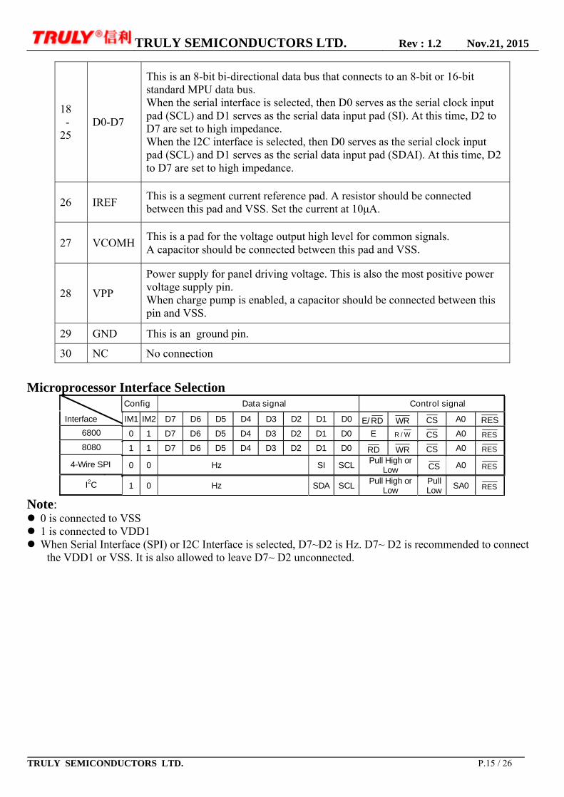
INTERFACE PIN CONNECTIONS No. Symbol Description
1 NC No connection
2 C2P
Connect to charge pump capacitor. These pins are not used and should be disconnedted when Vpp is supplied externally.
3 C2N
4 C1P
5 C1N
6 VBAT 3.0 – 4.2V power supply pad for Power supply for charge pump circuit.
7 NC No connection
8 GND This is a ground pin
9 VDD Power supply input: 1.65 - 3.5V
10 IM0
MCU bus interface selection pins. 11 IM1
12 IM2
13 CS# This is the chip select input.(active LOW)
14 RES# This is a reset signal input pad. When RES is set to “L”, the settings are initialized. The reset operation is performed by the RES signal level.
15 A0
This is the Data/Command control pad that determines whether the data bits are data or a command. A0 = “H”: the inputs at D0 to D7 are treated as display data. A0 = “L”: the inputs at D0 to D7 are transferred to the command registers. In I2C interface, this pad serves as SA0 to distinguish the different address of OLED driver.
16 WR#
This is a MPU interface input pad. When connected to an 8080 MPU, this is active LOW. This pad connects to the 8080 MPU WR signal. The signals on the data bus are latched at the rising edge of the WR signal. When connected to a 6800 Series MPU: This is the read/write control signal input terminal. When W R/ = “H”: Read. When W R/ = “L”: Write.
17 RD#
This is a MPU interface input pad. When connected to an 8080 series MPU, it is active LOW. This pad is connected to the RD signal of the 8080 series MPU, and the data bus is in an output status when this signal is “L”. When connected to a 6800 series MPU , this is active HIGH. This is used as an enable clock input of the 6800 series MPU. When RD = “H”: Enable. When RD = “L”: Disable.
TRULY SEMICONDUCTORS LTD. Rev : 1.2 Nov.21, 2015
TRULY SEMICONDUCTORS LTD. P.15 / 26
18 -
25 D0-D7
This is an 8-bit bi-directional data bus that connects to an 8-bit or 16-bit standard MPU data bus. When the serial interface is selected, then D0 serves as the serial clock input pad (SCL) and D1 serves as the serial data input pad (SI). At this time, D2 to D7 are set to high impedance. When the I2C interface is selected, then D0 serves as the serial clock input pad (SCL) and D1 serves as the serial data input pad (SDAI). At this time, D2 to D7 are set to high impedance.
26 IREF This is a segment current reference pad. A resistor should be connected between this pad and VSS. Set the current at 10μA.
27 VCOMH This is a pad for the voltage output high level for common signals. A capacitor should be connected between this pad and VSS.
28 VPP
Power supply for panel driving voltage. This is also the most positive power voltage supply pin. When charge pump is enabled, a capacitor should be connected between this pin and VSS.
29 GND This is an ground pin.
30 NC No connection
Microprocessor Interface Selection
langislortnoClangisataDgifnoC
Interface IM1 IM2 D7 D6 D5 D4 D3 D2 D1 D0 E/ RD WR CS A0 RES
6800 0 1 D7 D6 D5 D4 D3 D2 D1 D0 E WR / CS A0 RES
8080 1 1 D7 D6 D5 D4 D3 D2 D1 D0 RD WR CS A0 RES
4-Wire SPI 0 0 Hz SI SCLPull High or
Low CS A0 RES
I2C 1 0 Hz SDA SCLPull High or
LowPullLow
SA0 RES Note: 0 is connected to VSS 1 is connected to VDD1 When Serial Interface (SPI) or I2C Interface is selected, D7~D2 is Hz. D7~ D2 is recommended to connect
the VDD1 or VSS. It is also allowed to leave D7~ D2 unconnected.

TRULY SEMICONDUCTORS LTD. Rev : 1.2 Nov.21, 2015
TRULY SEMICONDUCTORS LTD. P.16 / 26
COMMAND TABLE
Code Command
A0 RD WR D7 D6 D5 D4 D3 D2 D1 D0 Function
1. Set Column Address 4 lower bits 0 1 0 0 0 0 0 Lower column address
Sets 4 lower bits of column address of display RAM in register. (POR = 00H)
2. Set Column Address 4 higher bits
0 1 0 0 0 0 1 Higher column addressSets 4 higher bits of column address of display RAM in register. (POR = 10H)
3. Set Pump voltage value
0 1 0 0 0 1 1 0 0 Pump
voltage value
This command is to control the DC-DC voltage output value. (POR=32H)
4. Set Display Start Line
0 1 0 0 1 Line address Specif ies RAM display line for COM0. (POR = 40H)
5. The Contra st Control Mode Set
0 1 0 1 0 0 0 0 0 0 1
Contrast Data Register Set
0 1 0 Contrast Data
This command is to set Contrast Setting of the display. The chip has 256 contrast steps from 00 to FF. (POR = 80H)
6. Set Segment Re-map (ADC)
0 1 0 1 0 1 0 0 0 0 ADC The right (0) or left (1) rotation. (POR = A0H)
7. Set Entire Display OFF/ON
0 1 0 1 0 1 0 0 1 0 D Selects normal display (0) or Entire Display ON (1). (POR = A4H)
8. Set Normal/ Reverse Display
0 1 0 1 0 1 0 0 1 1 D Normal indication (0) when low, but reverse indication (1) when high. (POR = A6H)
9 Multip lex Ration Mode Set
0 1 0 1 0 1 0 1 0 0 0
Multip lex Ration Data Set
0 1 0 * * Multip lex Ratio
This command switches default 63 mult iplex mode to any multiplex ratio from 1 to 64. (POR = 3FH)
10. DC-DC Control Mode Set
0 1 0 1 0 1 0 1 1 0 1
DC-DC ON/OFF Mode Set
0 1 0 1 0 0 0 1 0 1 D
This command is to control the DC-DC voltage DC-DC will be turned on when display on converter (1) or DC-DC OFF (0). (POR = 8BH)

TRULY SEMICONDUCTORS LTD. Rev : 1.2 Nov.21, 2015
TRULY SEMICONDUCTORS LTD. P.17 / 26
Code Command
A0 RD WR D7 D6 D5 D4 D3 D2 D1 D0 Function
11. Display OFF/ON 0 1 0 1 0 1 0 1 1 1 D Turns on OLED panel (1) or turns off (0). (POR = AEH)
12. Set Page Address 0 1 0 1 0 1 1 Page Address
Specifies page address to load display RAM data to page address register. (POR = B0H)
13. Set Common Output Scan Direction
0 1 0 1 1 0 0 D * * * Scan from COM0 to COM [N - 1] (0) or Scan from COM [N -1] to COM0 (1). (POR = C0H)
14. Display Offset Mode Set
0 1 0 1 1 0 1 0 0 1 1
Display Offset Data Set
0 1 0 * * COMx
This is a double byte command which specifies the mapping of display start line to one of COM0-63. (POR = 00H)
15. Set Display Divide Ratio/Oscillator Frequency Mode Set
0 1 0 1 1 0 1 0 1 0 1
Divide Ratio/Oscillator Frequency Data Set
0 1 0 Oscillator Frequency Divide Ratio
This command is used to set the frequency of the internal display clocks. (POR = 50H)
16. Dis-charge / Pre-charge Period Mode Set
0 1 0 1 1 0 1 1 0 0 1
Dis-cha rge /Pre-charge Period Data Set
0 1 0 Dis-cha rge Period Pre-charge Period
This command is used to set the duration of the dis-cha rge and pre-cha rge period. (POR = 22H)
17. Common Pads Hardware Configuration Mode Set
0 1 0 1 1 0 1 1 0 1 0
Sequential/Alternative Mode Set
0 1 0 0 0 0 D 0 0 1 0
This command is to set the common signals pad configuration. (POR = 12H)
18. VCOM Deselect Level Mode Set
0 1 0 1 1 0 1 1 0 1 1
VCOM Deselect Level Data Set 0 1 0 VCOM ( X VREF)
This command is to set the common pad output voltage level at deselect stage. (POR = 35H)
19. Read-Modify-Write 0 1 0 1 1 1 0 0 0 0 0 Read-Modify-Write start.
20. End 0 1 0 1 1 1 0 1 1 1 0 Read-Modify-Write end.
21. NOP 0 1 0 1 1 1 0 0 0 1 1 Non-Operation Command
22. Write Display Data 1 1 0 Write RAM data
23. Read Status 0 0 1 BUSYON/OFF * * * 0 0 0
24. Read Display Data 1 0 1 Read RAM data Note: Do not use any other commands, or the system malfunction may result.
Please find the detailed description of Commands in Specification of Driver IC SH1106G.

TRULY SEMICONDUCTORS LTD. Rev : 1.2 Nov.21, 2015
TRULY SEMICONDUCTORS LTD. P.18 / 26
INITIALIZATION CODE void InitOLED_MASTER_SH1106G(void) MainOLED_WCom(0xAE); //DOT MARTIX DISPLAY OFF MainOLED_WCom(0x33); //SET PUMP VOLTAGE MainOLED_WCom(0x40); //SET DISPLAY START LINE(40H-7FH) MainOLED_WCom(0x81); //CONTARST CONTROL(00H-0FFH) MainOLED_WCom(CONTRAST); MainOLED_WCom(0xA1); //SET SEGMENT RE-MAP(0A0H-0A1H) MainOLED_WCom(0xA4); //ENTIRE DISPLAY OFF(0A4H-0A5H) MainOLED_WCom(0xA6); //SET NORMAL DISPLAY(0A6H-0A7H) MainOLED_WCom(0xA8); //SET MULTIPLEX RATIO 64 MainOLED_WCom(0x3F); MainOLED_WCom(0xAD); //SET DC/D BOOSTER(8AH=OFF,8BH=ON) MainOLED_WCom(0x8A); MainOLED_WCom(0xC8); //COM SCAN COM1-COM64(0C8H,0C0H) MainOLED_WCom(0xD3); //SET DISPLAY OFFSET(OOH-3FH) MainOLED_WCom(0x00); MainOLED_WCom(0xD5); //SET FRAME FREQUENCY MainOLED_WCom(0x90); MainOLED_WCom(0xD9); //SET PRE_CHARGE PERIOD MainOLED_WCom(0x1F); MainOLED_WCom(0xDA); //COM PIN CONFIGURATION(02H,12H) MainOLED_WCom(0x12); MainOLED_WCom(0xDB); //SET VCOM DESELECT LEVEL(35H) MainOLED_WCom(0x40); Delayms(100);
MainOLED_WCom(0xAF); //DSPLAY ON

TRULY SEMICONDUCTORS LTD. Rev : 1.2 Nov.21, 2015
TRULY SEMICONDUCTORS LTD. P.19 / 26
SCHEMATIC EXAMPLE 8080 Series Interface Application Circuit(Internal Charge Pump):
Serial Interface Application Circuit(Internal Charge Pump):

TRULY SEMICONDUCTORS LTD. Rev : 1.2 Nov.21, 2015
TRULY SEMICONDUCTORS LTD. P.20 / 26
IIC Interface Application Circuit (Internal Charge Pump):
NOTE: 1. R1= (Voltage at IREF - VSS)/IREF≈510KΩ,C1=C2=0.22uF,
C3=C4=C5=C6=4.7uF, R2=R3=10K; 2. The VBAT VDD should connect a external voltage; 3. In Serial interface mode ,the read function is not possible. 4.The VCOMH capacitor is recommended to use tantalum capacitor to reduce noise. 5. The capacitor and the resistor value are recommended value. Select the appropriate value against module application.

TRULY SEMICONDUCTORS LTD. Rev : 1.2 Nov.21, 2015
TRULY SEMICONDUCTORS LTD. P.21 / 26
RELIABILITY TESTS
Item Condition Criterion
High Temperature Storage
(HTS) 80±2, 200 hours
1. After testing, the function test is ok.
2. After testing, no addition to the defect.
3. After testing, the change of luminance should be within +/- 50% of initial value.
4. After testing, the change for the mono and area color must be within (+/-0.02, +/-0.02) and for the full color it must be within (+/-0.04, +/-0.04) of initial value based on 1931 CIE coordinates.
5. After testing, the change of total current consumption should be within +/- 50% of initial value.
High Temperature Operating
(HTO) 70±2, 96 hours
Low Temperature Storage
(LTS) -30±2, 200 hours
Low Temperature Operating
(LTO) -20±2, 96 hours
High Temperature / High Humidity Storage
(HTHHS)
50±3, 90%±3%RH, 120 hours
Thermal Shock (Non-operation)
(TS)
-20±2 ~ 25 ~ 70±2
(30min) (5min) (30min)
10cycles
Vibration (Packing)
10~55~10Hz,amplitude 1.5mm, 1 hour for each direction x, y, z 1. One box for each test.
2. No addition to the cosmetic and the electrical defects. Drop (Packing)
Height : 1 m, each time for 6 sides, 3 edges, 1 angle
ESD (finished product housing)
±4kV (R: 330Ω C: 150pF , 10times, air
discharge)
1. After testing, cosmetic and electrical defects should not happen. 2. In case of malfunction or defect caused by ESD damage, it would be judged as a good part if it would be recovered to normal state after resetting.
Note:1) For each reliability test, the sample quantity is 3, and only for one test item. 2) The HTHHS test is requested the Pure Water(Resistance>10MΩ).
3) The test should be done after 2 hours of recovery time in normal environment.

TRULY SEMICONDUCTORS LTD. Rev : 1.2 Nov.21, 2015
TRULY SEMICONDUCTORS LTD. P.22 / 26
OUTGOING QUALITY CONTROL SPECIFICATION Standard
According to GB/T2828.1-2003/ISO 2859-1:1999 and ANSI/ASQC Z1.4-1993, General Inspection Level II.
Definition 1 Major defect : The defect that greatly affect the usability of product. 2 Minor defect : The other defects, such as cosmetic defects, etc. 3 Definition of inspection zone:
Zone A: Active Area
Zone B: Viewing Area except Zone A
Zone C: Outside Viewing Area
Note: As a general rule, visual defects in Zone C are permissible, when it is no trouble of
quality and assembly to customer`s product.
Inspection Methods 1 The general inspection : under 20W x 2 or 40W fluorescent light, about 30cm viewing
distance, within 45º viewing angle, under 25±5 .
2 The luminance and color coordinate inspection : By PR705 or BM-7 or the equal
equipments, in the dark room, under 25±5 . Inspection Criteria 1 Major defect : AQL= 0.65
Item Criterion
Function Defect
1. No display or abnormal display is not accepted
2. Open or short is not accepted.
3. Power consumption exceeding the spec is not accepted.
Outline Dimension Outline dimension exceeding the spec is not accepted.
Glass Crack Glass crack tends to enlarge is not accepted.
2 Minor Defect : AQL= 1.5
C
BA

TRULY SEMICONDUCTORS LTD. Rev : 1.2 Nov.21, 2015
TRULY SEMICONDUCTORS LTD. P.23 / 26
Item Criterion Spot Defect (dimming and lighting spot)
Size (mm) Accepted Qty
Area A + Area B Area C
X
Y
Φ≦0.07 Ignored
0.07<Φ≦0.10 3 Ignored0.10<Φ≦0. 15 1
0.15<Φ 0
Note : Φ= ( x + y ) / 2
Line Defect (dimming and lighting line)
L ( Length ) : mm W ( Width ) : mm Area A + Area B Area C
/ W≦0.02 Ignored
L≦3.0 0.02<W≦0.03 2 IgnoredL≦2.0 0.03<W≦0.05 1
/ 0.05<W As spot defect
Remarks: The total of spot defect and line defect shall not exceed 4 pcs. The distance between two lines defects must exceed 1 mm
Polarizer Stain
Stain which can be wiped off lightly with a soft cloth or similar cleaning is accepted, otherwise, according to the Spot Defect and the Line Defect.
Polarizer Scratch
1. If scratch can be seen during operation, according to the criterions of the Spot Defect and the Line Defect. 2. If scratch can be seen only under non-operation or some special angle, the criterion is as below : L ( Length ) : mm W ( Width ) : mm Area A + Area B Area C
/ W≦0.02 Ignore
3.0<L≦5.0 0.02<W≦0.04 2 Ignore L≦3.0 0.04<W≦0.06 1
/ 0.06<W 0
Polarizer Air Bubble
Size Area A + Area B Area C
X
Y
Φ≦0.20 Ignored
0.20<Φ≦0.30 2 Ignored0.30<Φ≦0.50 1
0.50<Φ 0

TRULY SEMICONDUCTORS LTD. Rev : 1.2 Nov.21, 2015
TRULY SEMICONDUCTORS LTD. P.24 / 26
Glass Defect (Glass Chiped )
1. On the corner (mm)
x ≤ 1.5
y ≤ 1.5
z ≤ t
2. On the bonding edge
(mm)
x ≤ a / 4
y ≤ s / 3 &≤0.7
z ≤ t
3. On the other edges
(mm)
x ≤ a / 8
y ≤ 0.7
z ≤ t
Note: t: glass thickness ; s: pad width ; a: the length of the edge
TCP Defect
Crack, deep fold and deep pressure mark on the TCP are not accepted
Pixel Size The tolerance of display pixel dimension should be within ±20% of the spec
Luminance Refer to the spec or the reference sample
Color Refer to the spec or the reference sample
TRULY SEMICONDUCTORS LTD. Rev : 1.2 Nov.21, 2015
TRULY SEMICONDUCTORS LTD. P.25 / 26
CAUTIONS IN USING OLED MODULE Precautions For Handling OLED Module:
1. OLED module consists of glass and polarizer. Pay attention to the following items when handling:
i. Avoid drop from high, avoid excessive impact and pressure. ii. Do not touch, push or rub the exposed polarizers with anything harder than an HB pencil lead.
iii. If the surface becomes dirty, breathe on the surface and gently wipe it off with a soft dry cloth. If it is terrible dirty, moisten the soft cloth with Isopropyl alcohol or Ethyl alcohol. Other solvents may damage the polarizer. Especially water, Ketone and Aromatic solvents.
iv. Wipe off saliva or water drops immediately, contact the polarizer with water over a long period of time may cause deformation.
v. Please keep the temperature within specified range for use and storage. Polarization degradation, bubble generation or polarizer peeling-off may occur
with high temperature and high humidity. vi. Condensation on the surface and the terminals due to cold or anything will damage,
stain or dirty the polarizer, so make it clean as the way of iii. 2. Do not attempt to disassemble or process the OLED Module. 3. Make sure the TCP or the FPC of the Module is free of twisting, warping and distortion,
do not pull or bend them forcefully, especially the soldering pins. On the other side, the SLIT part of the TCP is made to bend in the necessary case.
4. When assembling the module into other equipment, give the glass enough space to avoid excessive pressure on the glass, especially the glass cover which is much more
fragile. 5. Be sure to keep the air pressure under 120 kPa, otherwise the glass cover is to be cracked. 6. Be careful to prevent damage by static electricity:
i. Be sure to ground the body when handling the OLED Modules. ii. All machines and tools required for assembling, such as soldering irons, must be properly grounded.
iii. Do not assemble and do no other work under dry conditions to reduce the amount of static electricity generated. A relative humidity of 50%-60% is recommended.
iv. Peel off the protective film slowly to avoid the amount of static electricity generated. v. Avoid to touch the circuit, the soldering pins and the IC on the Module by the body. vi. Be sure to use anti-static package.
7. Contamination on terminals can cause an electrochemical reaction and corrade the terminal circuit, so make it clean anytime.
8. All terminals should be open, do not attach any conductor or semiconductor on the terminals.
9. When the logic circuit power is off, do not apply the input signals. 10. Power on sequence: VDD → VCC, and power off sequence: VCC → VDD. 11. Be sure to keep temperature, humidity and voltage within the ranges of the spec,
otherwise shorten Module's life time, even make it damaged. 12. Be sure to drive the OLED Module following the Specification and datasheet of IC
controller, otherwise something wrong may be seen.

TRULY SEMICONDUCTORS LTD. Rev : 1.2 Nov.21, 2015
TRULY SEMICONDUCTORS LTD. P.26 / 26
13.When displaying images, keep them rolling, and avoid one fixed image displaying more than 30 seconds, otherwise the residue image is to be seen. This is the speciality of OLED.
Precautions For Soldering OLED Module:
1. Soldering temperature : 260C 10C. 2. Soldering time : 3-4 sec. 3. Repeating time : no more than 3 times. 4. If soldering flux is used, be sure to remove any remaining flux after finishing soldering
operation. (This does not apply in the case of a non-halogen type of flux.) It is recommended to protect the surface with a cover during soldering to prevent any damage due to flux spatters.
Precautions For Storing OLED Module:
1. Be sure to store the OLED Module in the vacuum bag with dessicant. 2. If the Module can not be used up in 1 month after the bag being opened, make sure to
seal the Module in the vacuum bag with dessicant again. 3. Store the Module in a dark place, do not expose to sunlight or fluorescent light. 4. The polarizer surface should not touch any other objects. It is recommended to store the
Module in the shipping container. 5. It is recommended to keep the temperature between 0C and 30C , the relative humidity
not over 60%.
Limited Warranty Unless relevant quality agreements signed with customer and law enforcement, for a period of 12 months from date of production, all products (except automotive products) TRULY will replace or repair any of its OLED modules which are found to be functional defect when inspected in accordance with TRULY OLED acceptance standards (copies available upon request). Cosmetic/visual defects must be returned to TRULY within 90 days of shipment. Confirmation of such date should be based on freight documents. The warranty liability of TRULY is limited to repair and/or replacement on the terms above. TRULY will not be responsible for any subsequent or consequential events.
Return OLED Module Under Warranty:
1. No warranty in the case that the precautions are disregarded. 2. Module repairs will be invoiced to the customer upon mutual agreement. Modules
must be returned with sufficient description of the failures or defects.
PRIOR CONSULT MATTER 1. For TRULY standard products , we keep the right to change material ,process … for
improving the product property without any notice on our customer. 2. If you have special requirement about reliability condition, please let us know before
you start the test on our samples.