parametric amplification in mems devices
TRANSCRIPT
PARAMETRIC AMPLIFICATION IN MEMS
DEVICES
CHEO KOON LIN (B.Eng. (Hons.), NUS)
A THESIS SUBMITTED
FOR THE DEGREE OF MASTER OF ENGINEERING
DEPARTMENT OF MECHANICAL ENGINEERING
NATIONAL UNIVERSITY OF SINGAPORE
2003
brought to you by COREView metadata, citation and similar papers at core.ac.uk
provided by ScholarBank@NUS

Acknowledgements ________________________________________________________________________
Acknowledgements
This project would have been impossible if not for the contributions of many
people. First of all I would like to thank A/P Francis Tay Eng Hock. This project would
not have even taken off if not for his enthusiasm in allowing me to attempt something
akin to stepping off into the unknown. His undying support was truly heartening to a
student who had almost lost all hope in making sense of the world of MEMs.
To A/P Chau Fook Siong for accommodating all the blunders that were made
along the way. His earnest comments were invaluable every step of the way. My heartfelt
appreciation to Mr. Logeeswaran, our Research Engineer in MEMsLab. All the
discussions and help he offered were simply priceless. His passion for research simply
rubs off everyone in the lab, making it an enjoyable experience simply to be even there.
To YeeYuan, who never fails to amaze me with his breadth of knowledge. The
discussions with him over electronics were indispensable. It would have been impossible
for a mechanical engineer to make sense of the various aspects of electrical engineering
on his own. To Meilin for sharing all the secrets of detection schemes. To Jyh Siong, for
all the discussions we had. Many thanks to Prof C.H. Ling and Mdm Lian Kiat at MOS
lab in ECE, for their tolerance of an intruder to their MMR vacuum probe. To everyone
else who had helped in one way or another.
And finally to my family for their understanding of why I hadn’t been home.
i

Table of Contents
__________________________________________________
Table Of Contents Acknowledgements i
Table of Contents ii
Summary v
List of Figures vi
List of Tables ix
List of Symbols x
1. Introduction 1
1.1 Background 1
1.2 Noise and Reactance 2
1.3 Parametric Amplification 3
1.4 Objectives 4
1.5 Thesis Outline 5
2. Capacitive-Based MEMS 7
2.1 MEMS device variation 7
2.2 Single and Double Frequency Actuation 8
3. Parametric Amplifier Theory 10
3.1 Manley-Rowe equations 10
3.2 3-Frequency systems 11
3.2.1 Summing converters 12
3.2.2 Difference converters 13
3.3 Small-Signal Analysis 15
3.4 Up-Converter Parametric Amplifier 16
3.4.1 Input and Output Impedance 21
3.5 Negative-Resistance Parametric Amplifier 22
3.6 Degenerate Amplifier 24
3.7 Phase-Coherent Degenerate Amplifier 28
4. Modelling 31
4.1 Introduction 31
4.2 1-DOF Equivalent Electrical Model 31
ii

Table of Contents
__________________________________________________
4.3 Parasitic Capacitance 33
4.4 Parameter Extraction 35
4.5 Higher DOFs 38
4.5.1 Bond Graph Conversion 39
4.6 Non-Linear Modelling 43
5. Device Characterization 44
5.1 Initial Characterization 44
5.2 Resonance Detection 45
5.3 Lock-In Amplifier 46
5.4 3f Detection Scheme 47
5.5 Extraction of γn coefficients 49
5.5.1 Extraction method 52
5.6 Extracting Rc 54
6. Filter Design 56
6.1 Filter Design 56
6.1.1 Active Filters 56
6.2 PCB Design 59
7. Experiment Results 61
7.1 Device Selection 61
7.1.1 BARS Gyroscope 62
7.2 3f Detection results 63
7.2.1 Results for port 10-14 64
7.2.2 Results for port 18-14 64
7.2.3 Vacuum chamber testing 65
7.3 Device Parameters 67
7.3.1 Cp-D curve 67
7.3.2 Internal Resistance, Rc 68
7.3.3 Coefficients, γn 69
7.4 Filter Design 71
7.4.1 Circuit Board design 73
7.5 Up-converter Gain 75
iii

Table of Contents
__________________________________________________
7.5.1 Gain-Load & Gain-γ1 Relation 81
8. Conclusion 85
8.1 Future work 86
REFERENCES 87
APPENDIX A
Bond Graphs A1
iv

Summary ________________________________________________________________________
Summary Parametric amplification in a low capacitance MEMS parallel-plate device is
demonstrated. The behaviour of such small capacitance devices is shown to still follow
theoretical approximations. The general power gain of such a system is shown to be
dependent on load and capacitance change, γn. A means of estimating characterization of
capacitance change of the device at resonance (γn) through the extraction from current
parameters is proposed.
γ1 values ranging from 0.001 to 0.008 are obtained, which limits the effective gain
and characteristics of the parametric amplifier. However, as the device used was an
improvised gyroscope, the resonant frequency of ~1800 Hz and γ1 are not as high as
would have liked. Theoretical values predicted insufficient gain and are confirmed
through experiment.
A new resonance detection scheme is proposed, which removes the necessity for a
DC-bias to the device. The resonance characteristics of this 3f-detection scheme are
analysed and demonstrated. The simplicity and elegance of this scheme made possible the
detection of resonance for one-port devices with high parasitic capacitance. Previous
known methods were limited to 2-port devices only.
An Electrical Equivalent Modelling scheme is also proposed, based on Bond
Graph modelling. It allows the representation of mechanical systems in electrical domain,
a convenient methodology in MEMS. Though not a suitable method for parametric
devices, it is also suggested how mechanical parameters can be extracted from electrical
signals. Some future modifications will be required for appropriate application.
v

List of Figures ________________________________________________________________________
List of Figures Figure 1.1: Microwave parametric amplifier operating at 9480 MHz 1
Figure 1.2: A coil with a ferro-magnetic bar moving within it 3
Figure 2.1: Schematic for a single comb-drive 7
Figure 2.2: Schematic for a movable parallel plate 8
Figure 2.3: Schematic of a resonator driven on one side 8
Figure 2.4: Schematic for a single frequency actuation 9
Figure 3.1: Model which Manley-Rowe equations were based on 10
Figure 3.2: Summing converters: f2 > f1 12
Figure 3.3: Summing converters: f2 < f1 13
Figure 3.4: Difference converters: f2 < f1 14
Figure 3.5: Difference converters: f2 > f1 14
Figure 3.6: Schematic of up-converter circuitry 17
Figure 3.7: 4-terminal network model 18
Figure 3.8: Plot showing the theoretical relation between gain and load. 20
Figure 3.9: Circuit model for a negative resistance amplifier 23
Figure 3.10: Original voltage model 24
Figure 3.11: Equivalent current source model 25
Figure 3.12: Showing direction of current flow 26
Figure 3.13: Plot of phase related gain 30
Figure 4.1: Equivalent Electrical Model 33
Figure 4.2: Parasitic capacitance on top of resonating circuit 34
Figure 4.3: Frequency response of resonating circuit with parasitics 35
Figure 4.4: 2-DOF mechanical resonating structure 38
Figure 4.5: Two LCR circuit in series 39
Figure 4.6: Bond Graph model for a 1-DOF system 39
Figure 4.7: 2-DOF Bond Graph model 40
Figure 4.8: Equivalent networked representations 40
Figure 4.9: Equivalent 2-DOF Electrical Model 41
Figure 4.10: Frequency response of obtained circuit 42
vi

List of Figures ________________________________________________________________________
Figure 4.11: Schematic of coupled resonators 42
Figure 4.12: Equivalent model for coupled resonators 43
Figure 5.1: Schematic for 2f resonance detection scheme 44
Figure 5.2: Plot of extracted noisy current against time 51
Figure 5.3: Plot of processed Q(t) 51
Figure 5.4: Sample data multiplied by a sinusoidal waveform 52
Figure 5.5: Equivalent electrical model of device 54
Figure 6.1: Schematic for a KHN biquad 57
Figure 6.2: Schematic of pins layout 58
Figure 6.3: Sample screen shot of FilterPro program 59
Figure 6.4: Drawing of PCB in Protel 59
Figure 7.1: SEM of BARS gyroscope 62
Figure 7.2: Schematic of the 3f measurement setup 63
Figure 7.3: 3f detection for port 10-14 64
Figure 7.4: 3f detection for port 18-14 65
Figure 7.5: Pictures of MMR Vacuum Probe station 66
Figure 7.6a: Frequency response from 600-1000 Hz 66
Figure 7.6b: Frequency response at 880-900 Hz 67
Figure 7.7: C-V curve for port 10-14 68
Figure 7.8: Real and Imaginary impedance values 69
Figure 7.9: Schematic of setup to measure γ1 70
Figure 7.10: Plot of extracted γ1 variation with voltage 71
Figure 7.11: Bode plot for bandpass centered at 906 Hz 72
Figure 7.12: Bode plot for bandpass at 2.1 kHz 73
Figure 7.13: Assembled filters on PCB 73
Figure 7.14: Gain-phase for pass band at 906 Hz 74
Figure 7.15: Gain-phase for pass band of 2.1 kHz 74
Figure 7.16: Originally intended configuration 75
Figure 7.17: Schematic of experimental setup 76
Figure 7.18: Plot when only pump signal is sent in 79
Figure 7.19: Plot showing the shift in frequencies 79
vii

List of Figures ________________________________________________________________________
Figure 7.20: Plot showing output for 296 Hz 80
Figure 7.21: Plot comparing theoretical and experimental values for 5.0 Vpp. 82
Figure 7.22: Predicted and experimental optimal gain 83
Figure 7.23: Gain dependence on γ1 84
viii

List of Tables ________________________________________________________________________
List of Tables Table 4.1: Showing relations between Bond Graph, Mechanical and Electrical elements
32
Table 7.1: Pins layout of device 63
Table 7.2: List of extracted γ1 values 70
Table 7.3: Theoretical and Practical values of resistors 72
Table 7.4: Output impedance for different pump voltage 77
Table 7.5: Input impedances for fixed pump voltage 78
Table 7.6: List of gain obtained in dB 82
ix

List of Symbols ________________________________________________________________________
List of Symbols ε Permittivity of vacuum, 8.854×10⁻¹² F/m
h Planck’s constant, 6.626×10⁻³⁴ Js
k Boltzmann’s constant, 1.3807×10⁻²³ JK-1
L Inductance
C Capacitance
R Resistance
Q Charge
Z Impedance
V Voltage
I Current
k Spring Constant
m mass
c damping coefficient
P Power
w frequency
γn capacitance ratio, 02C
Cn
x

CHAPTER 1: Introduction ________________________________________________________________________
CHAPTER 1: Introduction
1.1 Background
The theory of parametric amplification is not new. The foundation of such
amplification systems had been laid since Manley and Rowe’s paper in 1956 [1], [2].
However, the relevance of such devices has changed with time. In the 1960s, great interest
was generated in such amplification in the search for low-noise amplification. The advent
of the maser (“microwave amplification by stimulated emission”) satisfied the noise
requirements for microwave engineers. The aim then was to obtain a means of achieving
the low-noise properties of the maser but yet retain the simplicity in application of a
transistor. That was a time when the semiconductor transistor was in its infant phase. Thus
there was a need for the pursuit of parametric amplifiers because it offered the theoretical
possibility of amplification at a low level of background noise. The relevance is noted in
transmission systems where the level of external noise is low, the main source of noise
being the receiver’s intrinsic noise sources (e.g. space telecommunication). The first
implementation of such parametric amplifiers used semiconductor varactors as the non-
linear capacitance device. [3].
With progress in the understanding and design of low-noise transistor circuits,
parametric amplification lost flavour. Moreover, early designs for microwave parametric
mentation. An early design by Philips
Corporation [28] is shown in Fig. 1.1.
However, such schemes still
continued to be ac
amplifiers were cumbersome and complex in imple
tively researched
and
Fig. 1.1. Microwave parametric amplifier operating at 9480 MHz
implemented in optical
transmission techniques today. An
example is an optical parametric
amplification (OPA) system. It is a
nonlinear interaction in which two
light waves of frequencies w1 and w2
are amplified in a medium which is
1
CHAPTER 1: Introduction ________________________________________________________________________
irradiated with an intense pump wave of frequency w3. [4][5].
1.2. Noise and Reactance
metric amplifier obtain low noise levels? It will first be How then does a para
necessary to understand the mechanisms of noise. In simple terms, Nyquist [6] showed
that the thermal noise power from a conductor at the physical temperature, T (K) is
fhfNN ∆== [W] 1.e kT
hff
−∆
11
where is Planck’s constant, is Boltzmann’s
t, f is the frequency
Jsh 3410626.6 −×= 123103807.1 −−×= JKk
constan and f∆ is the bandwidt stem, both in Hz.
For hf << kT, a condition which is satisfied at room temperature for frequencies less than
a comfortable 600 GHz, this is reduced to
kTN
h of the measuring sy
f= ∆ [W] 1.2
he noise power model for a one-port resistan
T ce is then given by the stochastic expression
R
e 2
N4
= [W] 1.3
where R is the resistance value of the element.
pl ed to be the main source of thermal noise.
eactance is an element that stores and transfers energy. In comparison, a resistor
is an e
In sim e terms, resistive elements are attribut
Amplification circuits today rely on semiconductors, which add shot noise [7] to the
system.
R
lement that dissipates energy. If the stored energy lies in an electric field, the
reactance is said to be capacitive in nature. Magnetic field storage elements are inductors.
A capacitive reactance may then be defined as an element for which a relation can be
written between charge, q and voltage, v, i.e.
( )vfq =
Similarly, an inductive element may be defined as one in which there is a relation between
flux, φ and current, i, i.e.
( )if=φ
2

CHAPTER 1: Introduction ________________________________________________________________________
The essential feature of parametric amplifiers is that it utilizes a non-linear pure
reactance, be it capacitive or inductive in nature. Since a pure reactance does not
constitute to thermal noise in a circuit, parametric amplifiers should realise a low-noise
amplification system.
Moreover, from (1.2), we see that thermal noise is a function of temperature.
Lowering the temperature cannot eliminate shot noise in semiconductor junctions.
Combining both of these conditions imply that there is a lower limit to which we can
reduce noise in transistor circuitry and their operating at high temperatures increases noise
levels. Therefore, realising parametric amplification is attractive for systems operating at
extreme temperatures.
1.3. Parametric Amplification
Parametric amplification as demonstrated here in this project is based on
capacitive devices. However, it can easily be extended to other forms of devices. The only
requirement is that the quantity to be measured is partly dependent on a certain
‘parameter’, thus the name parametric. Take, for example, the amount of magnetic flux
from an inductor coil.
Vac
Fig. 1.2. A coil with a ferro-magnetic bar moving within it
As a varying potential of a frequency wac is applied across the coil, magnetic flux is
induced in the coil. Suppose then that there is a ferro-magnetic bar moving in and out of
the coil at a frequency of wb. When the bar is within the coil, the effective permeability
within the coil changes and a stronger magnetic flux is induced. In this case, the parameter
which varies with time is the effective permeability within the coil, influenced by the
motion of the bar. Fig. 1.2 shows the schematic of such a situation.
3

CHAPTER 1: Introduction ________________________________________________________________________
Now consider the situation if the bar is also moving at a frequency , and
the amplitude coincides with the point where the bar is within the coil. If the phase
between them is such that the maximum amplitude of the bar is at the time when the V
acb ww 2=
ac
change is greatest, the amount of flux is effectively increased due to the presence of the
bar within the coil. To the ‘input’ (Vac), there appears to be gain because though it had
been supplying constant power into the coil throughout, the magnetic flux generated is
now apparently increased. This then is an example of a phase dependent parametric
system since the increase in flux depends on whether the phase of the bar coincides with
that of the applied voltage.
Various other forms of parametric amplification have been demonstrated before.
Among them, the amplification of a weak spin wave (SW) in ferrite films [8], quantum
dynamics [9], semiconductor junctions [10], microcantilevers [11] and MEMS devices
[12].
Even among MEMS-based parametric amplification systems, the diversity in
application is noted. Torsional oscillators [13], cantilevers [14], membranes [12] and a
coupled resonator [15] have all been targets for parametric amplification.
One aspect of parametric amplification lies in the fact that various signals going in
and out of the system must be free from one another’s interference. The interaction
between them must occur only within the device itself. As such, working in a single
energy domain will require the use of some sort of filtering capability to ensure that the
signals are decoupled within their own loops. An alternative would be to work in different
energy domains. Thus various means of detection and actuation have been attempted,
from piezo actuation [14] and detection [11] to light actuation [16] and detection [13].
1.4. Objectives
MEMS-based parametric amplifiers will greatly minimize the factors which
hampered the progress of previous attempts. In this report, we will explore the possibility
and constraints which make such MEMS-based parametric amplifiers an alternative for
low noise systems. The aim is to demonstrate the existence of parametric amplification for
low capacitance devices, of the order of a few pico-farads. The closest work to this is that
of Raskin et al [12] where they used a 1 cm2 size diaphragm as a parallel plate capacitor.
4

CHAPTER 1: Introduction ________________________________________________________________________
The initial phase of the project will be to understand and obtain a theoretical
background for the operation of parametric amplification. To do this, the theory is adapted
from one done by Blackwell [20] in which the operation using semiconductor diodes was
derived. Acquiring the theory will allows us to have a better perceptive in selecting the
best MEMS device available and spotting the potential pit-falls in the application.
Ultimately, the goal is to demonstrate that low capacitance MEMS devices have the
potential to be used as a parametric amplifier and verify that the operation agrees with
theory.
In the process of characterizing the device, two new methodologies are discussed.
Firstly, a novel method of measuring resonance through the measurement of signals at
three times the driving frequency (termed 3f) is demonstrated. Analysis of such detection
scheme is done and verified with experimental results. The simplicity of the scheme
allows it to be used for detecting resonance of one-port devices where parasitic
capacitance is high, which other methods [17], [18] are incapable of.
A second methodology suggested is an Electrical Equivalent Modelling technique.
By modelling mechanical parameters with electrical terms, it will be shown that it is
possible to extract the mechanical values through the detection of electrical signals.
However, this is limited to systems which are linear and where there is electrical-
mechanical coupling. The usefulness of Bond Graphs is demonstrated by extending this
capability to represent higher order systems.
1.5. Thesis Outline
The next chapter will introduce the analysis of excitation for capacitive-based
MEMS devices. This is necessary to understand the issues faced in the detection of
electrical signals as well as the 3f method of detection.
In Chapter 3, the relations for parametric amplification systems are derived.
Different configurations are analysed and the output relations are shown. Properties and
theoretical characteristics of such a device are discussed as well.
Chapter 4 then shows the modelling of resonating circuits and the implications of
parasitic capacitance. The electrical domain is shown to visualise such parasitics. A means
5

CHAPTER 1: Introduction ________________________________________________________________________
of using Bond Graphs to obtain equivalent higher degree-of-freedom systems is shown.
Derivations of such electrical representations are shown to extract mechanical parameters.
Several device parameters are required to analyse the device fully and this is
covered in Chapter 5. A novel 3f detection scheme is introduced and discussed. A means
of extracting the capacitance change ratio and internal resistance of the device is also
introduced.
The last component necessary for the implementation of parametric amplifications
is a filter. A basic outline of filters is covered in Chapter 6, and the resulting configuration
that is used in this project is shown and analysed. A printed-circuit-board (PCB) design
for the filters is presented.
Finally, Chapter 7 shows the final assembly of all the various issues discussed
together with the results for a MEMS parallel-plate parametric amplifier. The
experimental results for the various parameter extraction, resonance detection, filter
design and parametric amplification are presented.
Chapter 8 concludes the project and proposes suggestions for future work.
6

CHAPTER 2: Capacitive-Based MEMS ________________________________________________________________________
CHAPTER 2: Capacitive-Based MEMS
The implementation of parametric amplification requires the existence of a time-
varying capacitor. Capacitive-based MEMS devices suit this requirement perfectly. In this
section, an introduction to such actuation means is presented.
2.1. MEMS device variation
Estimation of the actuation for capacitive-based devices has been established since
Tang [19]. For any electrostatic capacitance, the energy stored, E, is known to be
2
21 CVE = 2.1
where is the capacitance between the plates and V is the potential difference between
them.
C
The actuation force is then
2
21 V
dxdC
dxdEF == 2.2
Actuation force then depends on the nature of the capacitance variation with
displacement, dxdC . For a comb-drive, the capacitance change is approximately constant,
within limits, as ( )
dxgh
C−
≈ 02ε, where h is the depth of the finger for a single comb as
shown in Fig. 2.1. Practical devices will contain many of such combs in parallel.
x
y
Fig. 2.1. Schematic for a single comb-drive
g0
d
For a purely parallel plate, the capacitance change will approximately vary inversely with
displacement since ( )xdAC−
=0
ε (neglecting fringing fields), as shown in Fig. 2.2.
7

CHAPTER 2: Capacitive-Based MEMS ________________________________________________________________________
x
y
Fig. 2.2. Schematic for a movable parallel plate
d0
2.2. Single and Double frequency actuation
Many capacitive-based devices like accelerometers and gyroscopes are necessarily
resonated, mostly at their resonance frequencies. The actuation due to the applied voltages
depends on the AC signal applied as well as the location of the placed voltages. For a 2-
port device, an AC could be placed on one end, with a DC-bias on the mass and current
detection at the other end (Fig. 2.3).
mass
output
combs combs
Transimpedance amplifier
VDC
Vac
Fig. 2.3. Schematic of a resonator driven on one side
The V2 term in (2.2) would be due to the difference in voltage of the AC and the DC
applied i.e.
dcac VwtVV −= sin
Expanding the resulting force equation (2.2), the actuation force would then have
components at frequencies of w and 2w, as shown below
⎟⎟⎠
⎞⎜⎜⎝
⎛−−+= wtVwtVV
VV
dxdCF acacdc
acdc 2cos
21sin2
221 2
22 2.3
8
CHAPTER 2: Capacitive-Based MEMS ________________________________________________________________________
The equilibrium position (which affects the mean capacitance, C0) is also affected by the
DC and AC voltages. Actuation is then at w as well as 2w. The capacitance variation,
which is dependent on the motion of the device, will also be at these two frequencies, i.e.
)2,()2,()2,( wwCwwxwwF ⇒⇒
However, not all configurations will result in actuation and capacitance change at
these frequencies. In another example, a 2-port device can be actuated only at 2w if only
an AC signal is applied to one side of the plate and the other side is grounded (Fig. 2.4).
output
Fixed plate
Movable plate
Transimpedance amplifier
Fig. 2.4. Schematic for a single frequency actuation
Vac
In this case, and therefore, wtVV ac sin=
⎟⎟⎠
⎞⎜⎜⎝
⎛−= wt
VVdxdCF acac 2cos
2221 22
2.4
which shows an actuating signal at 2w. In this scenario, the same AC signal affects the C0
as well as resonates the structure. As will be shown in the results later, such
approximations are not totally accurate. Due to the dxdC term being a function of x for a
parallel plate configuration, excitation still occurs at w, albeit at much lower amplitudes.
Nevertheless, the desired operation or signal can be flexible and dependent on the
requirement of the design and function of the device. We will see the application of such
actuation in the next few chapters.
9

CHAPTER 3: Parametric Amplifier Theory
________________________________________________________________________
CHAPTER 3: Parametric Amplifier Theory
Manley and Rowe laid the foundations for parametric amplification in their 1956
paper. It is a paper that describes the theoretical limit and performance of parametric
amplifiers. We begin by introducing the all-important Manley and Rowe’s equations.
Subsequently, we will see how the operating characteristics of MEMS devices fit into the
picture and develop a theoretical model for four configurations: Up-converter Parametric
Amplifier, Negative-Resistance Parametric Amplifier, Degenerate Amplifier and Phase-
Coherent Degenerate Amplifier.
3.1. Manley-Rowe equations
Since the proposal of such an amplification system by Manley and Rowe in 1956,
it has not been widely integrated due to various reasons, among them size, performance
and application restrictions. However, the possibility of low-noise, high amplification is
difficult to ignore. This is especially true in areas of space communications and systems
operating at high temperatures, high sensitivity and low signal to noise (SNR) ratios.
The equations Manley & Rowe derived were based on a very simple circuit model
as shown in Fig. 3.1.
Fig. 3.1. Model which Manley-Rowe equations were based on
2f1+ f2f2 - f1f1 + f2f2f1
Essentially, the model comprised a non-linear capacitor (denoted by C in the
figure) and two input sources, V1 and V2 operating at their own frequencies. f1, f2 and the
10

CHAPTER 3: Parametric Amplifier Theory
________________________________________________________________________
rest of the variations denotes some form of filters which restrict the power within each
node to exist at only that particular frequency. R’s denotes resistor for each node. The
number of such output nodes goes effectively to infinity to encompass all possible
permutations of frequencies f1 and f2.
The complete derivation can be found in [20]. The final result can be summed up
by the following two equations:
00
, =+∑ ∑
= −∞=n m ps
mn
mfnfnP
3.1
00
, =+∑ ∑
−∞= =n m ps
mn
mfnfmP
3.2
where positive Pn,m denotes power flowing into the non-linear capacitance and fs and fp
represent the signal and pump frequencies respectively, applied to the device. The choice
of which input is pump or signal is purely arbitrary. Expanding the equations for any n
and m values expresses power levels at the various combinations of signal and pump
frequencies.
Manley and Rowe’s results were remarkable for two reasons: they are valid
without specifying the exact characteristics of the non-linear capacitance as well as the
power levels involved.
From these two fundamental relations, i.e. equations (3.1) and (3.2), the
application of the theory then depends purely on the creativity of the designer. Though
four frequency configurations are possible, we will only look at three frequency devices
here [20]. The implications and characteristics of such parametric amplifiers will be
derived below.
3.2. 3-frequency systems
We first look at the general operational characteristics obtainable from Manley-
Rowe’s equations.
For a 3-frequency system, other than a signal frequency f1 and a pump frequency
of f2, the third frequency can be at the sum or difference of f1 and f2. Characteristics of
both summing and difference systems are discussed in this section. Summing converters
will be introduced first.
11

CHAPTER 3: Parametric Amplifier Theory
________________________________________________________________________
3.2.1. Summing converters
With only a third output frequency f3 (which is the sum of f1 and f2), the resulting
Manley-Rowe’s equations become:
03
3
1
1 =+fP
fP
3.3
03
3
2
2 =+fP
fP
3.4
Even for summing converters, there are two summing situations that can be implemented:
where and . 12 ff > 12 ff <
To see the implications of the configurations, we represent the power signals on a
power versus frequency plot, with arbitrary scales for the axes. As mentioned earlier,
power going into the non-linear capacitance is given as positive and power out of it is
negative. In this case, since we are supplying power at both the pump and signal
frequencies, equations (3.3) and (3.4) tell us that the power output at frequency f3 has to
be negative. The arrows in bold in Fig.3.2. are the input and output signals which we
should focus on, since the pump signal (f2) is not the signal we are concerned with during
amplification.
Fig. 3.2. shows the case of , 12 ff >
Power
f1 f2 f1 + f2 Frequency Fig. 3.2. Summing converters: f2 > f1
Fig. 3.3 shows the other case of 12 ff < ,
12

CHAPTER 3: Parametric Amplifier Theory
________________________________________________________________________
Power
f2 f1 f1 + f2 Frequency
Fig. 3.3. Summing converter: f2 < f1
For both cases, the effective impedance of the device seen by both the signal and pump
circuits is positive because power is dissipated at both frequencies and is therefore stable.
The power gain we are interested in is the power of the output signal over the input signal,
i.e. 1
3
PP
which can be shown to have the simple relation below
1
3
ff
gain = 3.5
which is just the ratio of the output and input frequencies. Such a configuration is termed
an up-converter. This is the simplest implementation of a parametric configuration and its
gain is always greater than unity, since f3 is always greater than f1. Optimally, we would
want to operate at the configuration where since a larger gain would be apparent.
It must be noted that the Manley-Rowe equations express the theoretical maximum
possible gain for such an operation. As will be shown later, the actual gain will always be
less than this.
12 ff >
3.2.2. Difference converters
In a similar fashion, we can operate at difference frequencies of 124 fff −= or
. For such configurations, the Manley-Rowe equations reduce to the form 214 fff −=
04
4
1
1 =−fP
fP
3.6
04
4
2
2 =+fP
fP
3.7
13

CHAPTER 3: Parametric Amplifier Theory
________________________________________________________________________
If power is supplied at the pump, f2, we see that power is delivered from the pump to both
the output f4 as well as the signal f1. What this means is that the device delivers power to
the signal rather than absorbing it. Again, there are two possible ways of
implementation: or . 12 ff < 12 ff >
Where in the case of , the power plot is shown in Fig. 3.4. 12 ff <
Power
f2 f1 – f2 f1 Frequency
Fig. 3.4. Difference converters: f2 < f1
The input power at f1 is higher than the output power f4 and the difference is fed
into the pump. Therefore, the effective impedance seen from the pump circuit is a
negative resistance device. However, because the device itself would always possess a
loss resistance, there is a possibility that the circuit might still remain stable if the signal is
small enough or the internal resistance of the device is large enough. In addition, the gain
would always be less than unity since 11
21 <−f
ff, as evident from the plot.
For the case of , the power plot is shown in Fig. 3.5. 12 ff >
f2f1 f2 - f1 Frequency
Power
Fig. 3.5. Difference converters: f2 > f1
In this case, power is received by the signal as well as the output. The system is
also then potentially unstable. It will be shown in the case of a Phase-Coherent
14

CHAPTER 3: Parametric Amplifier Theory
________________________________________________________________________
Degenerate Amplifier that the gain can be made as great as possible, whatever the ratio of
the input and output frequencies.
What must be noted here is that there is no actual generation of power. Looking at
the overall picture, there is simply a mixing of power after going through the non-linear
device. Power is taken from certain output frequencies and transferred to others i.e. there
is no change in the net power in the system. When the ‘correct’ frequencies are chosen,
there appears to be amplification in the signal involved.
In the next few sections, detailed analysis and theoretical derivation of the various
characteristics of parametric amplifiers are presented.
3.3. Small-Signal Analysis
We begin with the derivation for a general case. In this section, we approximate
the case whereby the signal input is much lower than the pump signal; thus the analysis
uses small signal approximations. The direction of the derivations is from Blackwell [20].
We attempt to derive a general formulation for gain of a parametric amplifier. As
noted in the previous chapter, for a MEMS capacitive device, an approximation of the
capacitance variance can consist mainly of two frequencies (neglecting all other
harmonics)
( )twtwCtC 22210 2cos2cos21)( γγ ++= 3.8
The coefficients γn represent the variation in capacitance at each frequency. The factor of
2 is included to simplify derivations later.
To derive a general formulation for the device, let the possible operating potentials
be expressed as
twVtwVtwVtv 332211 cos2cos2cos2)( ++= 3.9
The numbers of the subscripts represent the usual signals at the various potentials.
We know that current at output will be given by
[ ]dt
tdCtvdt
tdvtCtvtCdtdti )()()()()()()( +== 3.10
Using small signal analysis, we write in phasor form,
15

CHAPTER 3: Parametric Amplifier Theory
________________________________________________________________________
[ ] [ twjtwjtjwtjw eeCeeCCtC 2222 2220100)( −− ++++= γγ ]
tjwtjwtjwtjwtjwtjw eVeVeVeVeVeVtv 334411 *33
*44
*11)( −−− +++++=
tjwtjwtjwtjwtjwtjw eIeIeIeIeIeIti 334411 *33
*44
*11)( −−− +++++=
Noting that and 321 www =+ 412 www =− , we are only interested in the real components
of I1 and I3 and the imaginary component of I4, i.e. tjwtjwtjw eIeIeIti 341
3*41)( ++= −
Noting that
321 www =+
412 www =−
4322 www +=
the resulting relevant current components are
1*
41013101101 wVjCwVjCwVjCI γγ ++=
3*
42033031103 wVjCwVjCwVjCI γγ ++=
4*
4043204110*4 wVjCwVjCwVjCI −−−= γγ
The admittance matrix of the device can then be written as
3.11 ⎥⎥⎥
⎦
⎤
⎢⎢⎢
⎣
⎡
⎥⎥⎥
⎦
⎤
⎢⎢⎢
⎣
⎡
−−−=
⎥⎥⎥
⎦
⎤
⎢⎢⎢
⎣
⎡
*4
3
1
40420410
32030310
11011010
*4
3
1
VVV
wjCwjCwjCwjCwjCwjCwjCwjCwjC
III
γγγγγγ
This general formulation will be utilized for the Up-Converter and the Negative-
Resistance configurations.
3.4. Up-Converter Parametric Amplifier
For an up-converter, the output frequency is at the sum of f1 and f2. The circuit for
such a configuration is shown in Fig. 3.6.
16

CHAPTER 3: Parametric Amplifier Theory
________________________________________________________________________
Fig. 3.6. Schematic of up-converter circuitry
The time-varying capacitor is pumped at a certain frequency f2, not noted in the
schematic. Rg represents the internal resistance of the input signal. X1 and R1 represent the
reactance and resistance of the input circuit respectively and Rc represents the internal loss
of the device. Rl is the load.
For an up-converter working on only two frequencies, the matrix (3.11) reduces to
3.12 ⎥⎦
⎤⎢⎣
⎡⎥⎦
⎤⎢⎣
⎡=⎥
⎦
⎤⎢⎣
⎡
3
1
30310
11010
3
1
VV
wjCwjCwjCwjC
II
γγ
in which the relevant frequencies concerned are at the input frequency f1 and the summed
frequency f3.
By inversing, the impedance matrix is then
⎥⎦
⎤⎢⎣
⎡⎥⎦
⎤⎢⎣
⎡=⎥
⎦
⎤⎢⎣
⎡
⎥⎥⎥⎥
⎦
⎤
⎢⎢⎢⎢
⎣
⎡
−−−
−−
−=⎥⎦
⎤⎢⎣
⎡
3
1
2221
1211
3
1
21
203
2101
1
2103
12101
3
1
)1(1
)1(
)1()1(1
II
ZZZZ
II
CjwCjw
CjwCjwVV
γγγ
γγ
γ 3.13
where subscripts 1 and 3 denote the voltages and currents at input and output frequencies
respectively. The impedance relation models a four terminal network. Such a system can
be depicted as in Fig. 3.7.
17

CHAPTER 3: Parametric Amplifier Theory
________________________________________________________________________
Fig. 3.7. A four terminal network model
Now, if we were to include all the various impedances into our 4-port model, (3.13) will
have the form
3.14 ⎥⎦
⎤⎢⎣
⎡⎥⎦
⎤⎢⎣
⎡+
+=⎥
⎦
⎤⎢⎣
⎡
3
1
32221
12111
3
1
II
ZZZZZZ
VV
T
T
where
cgT RRXRZ +++= 111 3.15
clT RRXRZ +++= 333 3.16
Now, we attempt to find the power gain at the load of the system. The maximum
power input possible (from the maximum power theorem) is gg R
VR
V4
12
21
21 = . The power
output at the load is lRI 23 .
The power gain is then, 21
234
V
IRRg lg
t =
It is necessary then to express a relation that relates the current output I3 in terms
of input voltage V1. From (3.14), and letting 03 =V (as there is no actual source voltage at
output), we can show that
( )( ) 1221111322
1213 ZZZZZZ
VZITT −++
−= 3.17
The gain is then of the form
18

CHAPTER 3: Parametric Amplifier Theory
________________________________________________________________________
( )( ) 2
1221111322
2214
ZZZZZZ
ZRRg
TT
glt
−++= 3.18
For the circuit to be operating at resonance, there should not be any reactance, i.e.
0111 =+ XZ and . Also substituting the other impedances into the equation,
we obtain the approximate value of g
0322 =+ XZ
t as
( )( )2
231
21
13
2
1
14
CwwRRRRRR
CwRR
g
cgcl
gl
tγ
γ
+++++
= 3.19
where
( )210 1 γ−= CC 3.20
We can, if appropriate for the device in question, make another assumption that
the circuit losses are negligible compared to the device losses, i.e. cl RRR +<<3 and
. The gain equation would then look like the following, after simplification cg RRR +<<1
( )( )2
3
1
1
1
4
⎥⎦
⎤⎢⎣
⎡+++
=
CwCw
RRRR
RRg
cgcl
glt
γγ
3.21
To find the maximum gain gt, we are interested to know what load and internal
resistance values would maximize gain. This is a characteristic which differentiates
parametric amplification from ‘normal’ circuits. The load that achieves maximum power
transfer is not fixed with respect to the internal load of the source, but can be changed by
varying another parameter, γ1. We can obtain optimal expressions for Rl and Rg from
(3.21) separately.
( )
( )1
1
3
1
1
12
γ
γγ
CwRR
CwCw
RRRR
cg
ccg
l
+
++= 3.22
19

CHAPTER 3: Parametric Amplifier Theory
________________________________________________________________________
The expression for Rg is similar (simply substituting terms containing Rg with Rl). In this
case, the gain is optimized for a given source impedance Rg and γ1. The corresponding Rl
is then obtained for this set of values.
Fig. 3.8. Plot showing the theoretical relation between gain and load.
Fig. 3.8 shows the relation between gain and load resistance Rl when the source
impedance is fixed at values of 50 Ω and 100 Ω and 002.01 =γ . In essence, there is an
optimal Rl that achieves maximum gain for different values of source impedance.
Alternatively, we can also obtain an expression where both optimal resistance
values ‘meet’. This would also imply that whatever expression which maximizes for Rl
would do the same for Rg. Then lg RR = for maximum gain. Differentiating gt with
respect to Rg in equation (3.21) to find the optimal Rg gives
2231
211
ccg RCww
RRγ
+= 3.23
This expression then dictates the values of Rg and Rl which will optimize the gain for a
given γ.
20

CHAPTER 3: Parametric Amplifier Theory
________________________________________________________________________
To show that the gain is truly bounded by Manley-Rowe’s equations, defining
cCRwQ
1
1= as the effective Q of the capacitive device at w1, we have
( )21
3
11 QwwRR cg γ+= 3.24
We then substitute this expression back into (3.21),
[ ]21
3
11 x
xww
gt++
= 3.25
where ( )21
3
1 Qwwx γ⎟⎟
⎠
⎞⎜⎜⎝
⎛= .
The term [ ] 111
2 →++ x
x as ∞→x , by applying L’Hopital’s rule.
Since the value of γ1 is bounded (from 0 to 0.5, from the definition), to obtain an infinite
value of x, we would require ∞→Q , which implies a lossless device.
Thus it is shown that a parametric amplification system is limited by Manley-
Rowe equations. In practice, to get the maximum gain possible from the system, we
would require the parameter 1γ be as large as possible, which implies that the device is
operating at resonance. Therefore, the pump frequency f2 will give optimal performance if
operated at the resonant frequency of the structure.
3.4.1 Input and Output Impedances
It was shown previously that a standard 4-terminal network model could
approximate the device characteristics. The effective input impedance can be obtained
through the standard form of
422
211211
Tin ZZ
ZZZZ+
−= 3.26
Substituting the relevance parameters from (3.13) into (3.26) we have,
⎟⎟⎠
⎞⎜⎜⎝
⎛+
+=
CjwZCww
CjwZ
T
in
33
231
2
1 11 γ 3.27
21

CHAPTER 3: Parametric Amplifier Theory
________________________________________________________________________
At circuit resonance, we are left with only the real values, which will be
3
231
2
Tin RCww
R γ= 3.28
which is a positive value.
By symmetry, the effective output impedance the capacitor presents to the output
circuit at resonance is then
1
231
2
Tout RCww
R γ= 3.29
Since both effective input and output resistance values are positive, the operation
of the up-converter device is stable.
3.5. Negative-Resistance Parametric Amplifier
For this mode of operation, the output frequency is at the difference frequencies of
pump and signal. As the name suggests, the effective impedance of the device will be
shown to be negative. For such a case, the matrix is given as
3.30 ⎥⎦
⎤⎢⎣
⎡⎥⎦
⎤⎢⎣
⎡−−
=⎥⎦
⎤⎢⎣
⎡*
4
1
40410
11010*4
1
VV
wjCwjCwjCwjC
II
γγ
and the impedance matrix as
⎥⎦
⎤⎢⎣
⎡⎥⎦
⎤⎢⎣
⎡=⎥
⎦
⎤⎢⎣
⎡
⎥⎥⎥⎥
⎦
⎤
⎢⎢⎢⎢
⎣
⎡
−−
−−
−−=⎥⎦
⎤⎢⎣
⎡*4
1
2221
1211*4
1
21
204
2101
1
2104
12101
*4
1
)1(1
)1(
)1()1(1
II
ZZZZ
II
CjwCjw
CjwCjwV
V
γγγ
γγ
γ 3.31
As in the case of the up-converter, the matrix equation has to include the various
impedances in the circuit. In this case, the circuit model is depicted in Fig. 3.9.
22

CHAPTER 3: Parametric Amplifier Theory
________________________________________________________________________
Fig. 3.9. Circuit model for a negative resistance amplifier
Thus,
3.32 ⎥⎦
⎤⎢⎣
⎡⎥⎦
⎤⎢⎣
⎡+
+=⎥
⎦
⎤⎢⎣
⎡*4
1
42221
12111*
4
1
II
ZZZZZZ
V
V
T
T
where
cgT RRXRZ +++= 111
clT RRXRZ +++= 444
With , we write I0*4 =V 1 as a function of V1,
( )( ) 2112422111
2111 ZZZZZZ
ZVITT −++
−= 3.33
The power gain is given by
1
224
VIRR
g lgt =
( )( ) 2
2112422111
2214
ZZZZZZ
ZRR
TT
lg
−++= 3.34
At resonance then,
[ ]21
4
1
4
4
RRRRRR
wwg
T
Tlg
t−
⎟⎟⎠
⎞⎜⎜⎝
⎛
= 3.35
23

CHAPTER 3: Parametric Amplifier Theory
________________________________________________________________________
where 4
241
2
TRCwwR γ= .
This configuration is not particularly interesting beyond the fact that the input
source ‘sees’ a negative impedance. As such the system is possibly oscillatory and
unstable.
3.6. Degenerate Amplifier
We now look at a different possible configuration of parametric amplifiers: a
degenerate amplifier. The configuration operates at the difference frequency of
. There are again two subsets which can occur. Firstly, the relation between
pump and signal is such that the output frequency f
124 fff −=
4 lies within the passband of the signal
or vice versa. Another, termed a phase-coherent amplifier, lies in the fact that the desired
operating output frequency f4 is also the input frequency at f1. Therefore, filters will not be
able to tell the difference between the two signals. Some interesting characteristics result.
To analyse the configuration, we look at the circuit model which will be used to
derive the operating characteristics.
We will go on to show that the gain characteristic is dependent on the phase
difference of the pump and signal. As such, we will use trigonometric representations with
phase information to derive the gain relations.
Fig. 3.10. Original voltage model
In this case, instead of using the usual voltage model in Fig. 3.10, we look at a current
equivalent circuit model as shown in Fig. 3.11. This is done so as to express the phase-
relations for the current output explicitly.
24

CHAPTER 3: Parametric Amplifier Theory
________________________________________________________________________
)sin( 11 φ+twV
i(t)
Fig. 3.11. Equivalent current source model
As before, we are interested in the power gain. In a similar fashion, the maximum
power that can be supplied by the source, this time an equivalent current source
is 1
2
2R
ig⎟⎟⎠
⎞⎜⎜⎝
⎛.
The power output at resistor R4 is 4
21
RV . Therefore, the power gain is
41
2
214
RRi
Vgg
t = 3.36
An expression that relates current to voltage will result in a full equation of the power
gain of the configuration. We proceed to derive current in terms of voltage. From this
point on, we will depart from the derivations of Blackwell [20]. There are several errors in
his derivations, the main one being adding an unknown phase to the capacitance change
expression.
As a convention, positive voltage will be represented as depicted in Fig. 3.11.
Again, we know that
[ ]dt
tdCtvdt
tdvtCtvtCdtdti )()()()()()()( +==
where positive current is ‘downward’ as shown in the Fig. 3.11.
Let the capacitance change be
( )twtwCtC 22210 2sin2sin21)( γγ ++=
The filters allow the presence of frequencies at w1 and w4, i.e.
25

CHAPTER 3: Parametric Amplifier Theory
________________________________________________________________________
)sin()sin()( 444111 φφ +++= twVtwVtv
where the unknown phase changes are included as some unknown phases φ1 and φ4.
Looking at dtdvC first, the various relevant components are
( ) ( )[ ]444411110 coscos φφ +++ twwVtwwVC
( ) ( )[ ]1121121101 )(sin)(sin φφγ −−++++ twwtwwwVC
( ) ( )[ ]4424243301 )(sin)(sin φφγ −−++++ twwtwwwVC 3.37
Relevant components within dtdCv are
( ) ( )[ ]1121212101 )(sin)(sin φφγ −−−+++ twwtwwwVC
( ) ( )[ ]4424242401 )(sin)(sin φφγ −−−+++ twwtwwwVC 3.38
For reasons which will be apparent later, the current through the device that is relevant to
us is only those at and )( 12 ww − )( 42 ww − i.e.
[ ] [ ]44244011121101 )(sin)(sin φγφγ −−+−− twwwVCtwwwVC [ ] [ ]44224011122101 )(sin)(sin φγφγ −−−−−− twwwVCtwwwVC 3.39
which can be further simplified to give
( ) ( )411401144101 sinsin φγφγ −−−−= twwVCtwwVCi 3.40
The negative sign means that instead of current flowing ‘into’ the device, it is actually
supplying current to the system. This is visualized in Fig. 3.12.
( ) ( 411401144101 sinsin φγφγ −+−+= twwVCtwwVCi )
Fig. 3.12. Circuit model showing direction of current flow
26

CHAPTER 3: Parametric Amplifier Theory
________________________________________________________________________
Now, based on the assumed potential, the current flowing into the individual resistors are
( ) ( )441
411
1
1 sinsin1
φφ +++= twRVtw
RViR
and
( ) ( )444
411
4
1 sinsin4
φφ +++= twRVtw
RViR
The components at w4 frequency are not from the input, thus it must have been ‘sourced’
from the varying capacitor. So we have
( ) ( 1441014441
4 sinsin11 φγφ −=+⎟⎟⎠
⎞⎜⎜⎝
⎛+ twwVCtw
RRV ) 3.41
From the above equation (3.41), we can obtain expressions relating (V4, φ4) to (V1, φ1)
⎪⎪⎩
⎪⎪⎨
⎧
⎟⎟⎠
⎞⎜⎜⎝
⎛+
−=
⎟⎟⎠
⎞⎜⎜⎝
⎛+
=⇒
⎪⎪⎩
⎪⎪⎨
⎧
−=⎟⎟⎠
⎞⎜⎜⎝
⎛+
=⎟⎟⎠
⎞⎜⎜⎝
⎛+
⇒
41
411410144
41
411410144
14101441
4
14101441
4
sinsin
coscos
sinsin11
coscos11
RRRR
wVCV
RRRR
wVCV
wVCRR
V
wVCRR
V
φγφ
φγφ
φγφ
φγφ
3.42
Now we can look at the expression for the source current, which can only be sourcing at
w1
ig(w1) ( ) ( ) ( 411401114
111
1
1 sinsinsin φγφφ −−+++= twwVCtwRVtw
RV )
( ) ( 4141011141
1 sinsin11 φγφ −−+⎟⎟⎠
⎞⎜⎜⎝
⎛+= twVwCtw
RRV ) 3.43
The whole purpose of (3.42) is to substitute into (3.43) to express everything in terms of
V1.
We know that
27

CHAPTER 3: Parametric Amplifier Theory
________________________________________________________________________
( ) [ ]41414414 sincoscossinsin φφφ twtwVtwV −=−
[ ]111141
414101 sincoscossin φφγ twtw
RRRRwVC ++
=
( )1141
414101 sin φγ +
+= tw
RRRRwVC
Therefore, the final expression for the source current is
ig(w1) ( ) ( ) ( 111412
0141
4111
411 sinsin11 φγφ +⎟⎟
⎠
⎞⎜⎜⎝
⎛+
−+⎟⎟⎠
⎞⎜⎜⎝
⎛+= twVwwC
RRRRtw
RRV ) 3.44
The gain expression is then
( )2
412
0141
41
41
4141
4
⎥⎦
⎤⎢⎣
⎡⎟⎟⎠
⎞⎜⎜⎝
⎛+
−⎟⎟⎠
⎞⎜⎜⎝
⎛ +=
wwCRR
RRRR
RRRR
gt
γ
3.45
Thus we have derived the gain equation for a case where 41 ww ≠ .
3.7. Phase-Coherent Degenerate Amplifier
A more interesting case is of a phase-coherent amplifier, 241 21 www == .
In this manner, there is a presence of only
( )111 sin)( φ+= twVtv
The mixing of the signal and capacitance produces a current at
( )1110111 sin)( φγ −−= twVCwwic
The generator current is then
( ) ( 111101110141
1 sinsin11 φγφ −−+⎟⎟⎠
⎞⎜⎜⎝
⎛++= twVwCtwCw
RRVig )
In this case, the gain is dependent on the phase of the signal. To see that relation, we have
to work in complex notation,
⎥⎦
⎤⎢⎣
⎡−⎟⎟
⎠
⎞⎜⎜⎝
⎛++= − 111
10110141
111 φφ γ jjtiw
g ewCVeCwRR
Vei
To get the magnitude of current, we take the conjugate,
28

CHAPTER 3: Parametric Amplifier Theory
________________________________________________________________________
⎥⎥⎥⎥⎥
⎦
⎤
⎢⎢⎢⎢⎢
⎣
⎡
⎟⎟⎟⎟⎟
⎠
⎞
⎜⎜⎜⎜⎜
⎝
⎛
⎟⎟⎠
⎞⎜⎜⎝
⎛++
+
⎟⎟⎠
⎞⎜⎜⎝
⎛++
−⎥⎦
⎤⎢⎣
⎡⎟⎟⎠
⎞⎜⎜⎝
⎛++==
2
0141
1012
0141
101
2
0141
1*2
11112
1111
CwRR
wCe
CwRR
wCCw
RRViii j
gggγγ φ
Now, if we let
01
41
101
11 CwRR
wC
++=
γβ 3.46
the expression can be rewritten as
[ ])2sin(2111
4
241
2
0141
φββ −+⎟⎟⎠
⎞⎜⎜⎝
⎛++
=
RRCwRR
gt 3.47
which shows gain being a function of the phase difference between the signal and the
pump frequency.
To determine the phase which will give us maximum gain, we want the
denominator to be as small as possible, therefore
1)2sin( =φ
4πφ =⇒
To maximise the gain at optimal phase, i.e.
[ ] [ ]241
2
0141
241
2
0141
111
4
2111
44
−⎟⎟⎠
⎞⎜⎜⎝
⎛++
=
−+⎟⎟⎠
⎞⎜⎜⎝
⎛++
=⎟⎠⎞
⎜⎝⎛ =
βββ
πφ
RRCwRR
RRCwRR
gt
29

CHAPTER 3: Parametric Amplifier Theory
________________________________________________________________________
β should be as close to 1 as possible. Parameters which we can vary easily are C0, w1 and
γ1. Figure 3.13 shows the phase-related gain.
Fig. 3.13. Plot of phase related gain
This configuration demonstrates a highly phase-selective amplifier if certain parameters
are met. Possible uses can be as for a phase-lock loop system.
30

CHAPTER 4: Modelling ________________________________________________________________________
CHAPTER 4: Modelling 4.1. Introduction
MEMS is a field which crosses multiple disciplines; from mechanical to electrical
to materials science. In actuation and sensing of capacitive-based devices, there is
coupling between the mechanical and electrical domains which has to be addressed.
Modelling of such devices then would have to take into account such multi-energy effects.
In this section, a means of incorporating mechanical aspects in the electrical domain will
be presented. Its usefulness will be explored for simple linear systems.
The proposed approach makes use of Bond Graphs [21], a modelling technique
first formulated by Professor Henry Paynter in the 1950s. Bond Graphs allows the ability
to represent multi-energy domains in a single graphical form and also obtain state-space
equations from them.
4.2. 1-DOF Equivalent Electrical Model
Bond graphs provide a means of representing multi-energy domains in a single
pictorial format. The usefulness is therefore apparent in MEMS, where we are dealing
with coupled systems. However, the final detection is always performed on electrical
systems and that is where all the various cross-coupling within the system, is finally
‘seen’. What will be presented here is a method of representing and analysing mechanical
systems in the electrical domain.
The well-known mechanical vibration equation for a single degree-of-freedom
(DOF), i.e.
0Fkxxcxm =++ &&& 4.1
where the notations represent the usual forms, is a simple representation of a linear
mechanical device. It is the basis of MEMS resonating structures. In Table 4.1 we
compare and see the relations between Bond Graph elements, electrical elements and
mechanical elements (see also Appendix A).
31
CHAPTER 4: Modelling ________________________________________________________________________
Table 4.1: Showing relations between Bond Graph, Mechanical and Electrical elements
Symbol Bond Graph Mechanical Electrical
Effort Force, F Potential, v
Flow
e
f Velocity, x& Current, Qi &=
General Relation Linear Relation
Resistor ( )fe Rφ= Rfe = xcF &= QRiRv &==
Capacitor
( )eq Cφ=( )qe C
1−= φ q
Ce 1= kxF =
dtdvCi =
QC
idtC
v 11==⇒ ∫
Inductor
( )fp Iφ=
( )pf I1−= φ
Ifp =
Ipf =
xmF &&= QLdtdiLv &&==
What is seen is a one-to-one relation between elements in the two domains:
capacitor equivalent to springs, resistors equivalent to dampers and inductors behaving
similar to mass. Bond Graph modelling utilizes such multi-domain characteristics. Of
course, these relations are not exhaustive. Fluid dynamics, thermodynamics, optics, etc all
have their equivalent elements. Electrical and mechanical domains are shown here
because these are the two main domains which MEMS devices operate in.
What is intended here is to demonstrate a means of representing simple
mechanical systems entirely using electrical components. This approach is not new. Clark
[22] had already used such electrical schematics to represent mechanical resonating
devices. From an electrical background, his objective was to visualise mechanical systems
in the electrical domain. However, this chapter will show that its capability can be
extended beyond just visualisation.
We will begin by looking at single-DOF mechanical devices, where the equation
of motion is the simple (4.1)
0Fkxxcxm =++ &&&
The equation says that the “summation of the forces due to inertia, damper and spring of
the system must be equal to the external forces” acting on the system. From Table 4.1
32

CHAPTER 4: Modelling ________________________________________________________________________
above, we know that there should be an equivalent electrical model. To paraphrase the
line above: “summation of the potential due to inductor, resistor and capacitor of the
system must be equal to the external potentials” i.e.
Vcapacitorresistorinductor =++
or in terms of conventional parameters,
∫ =++ VidtC
RidtdiL 1
Such a circuit then would be an inductor, capacitor and resistor (LCR) connected in series,
as shown in Fig. 4.1 below
Fig. 4.1. Equivalent electrical model
Both electrical and mechanical models exhibit the characteristic of resonance, as
expected. We will see below how this electrical model helps us better visualize the
concept of parasitics.
4.3. Parasitic Capacitance
The presence of parasitic capacitance greatly complicates the detection and
performance of capacitive-based devices. Parasitic exists between probe tips, wiring,
static structures on the devices, etc. It is unavoidable but its effects can be minimized
through proper design and consideration of possible causes. Depending on the situation,
parasitics can range from a few picofarads to even hundreds of picofarads. Thus, for a
device which has perhaps a few picofarads of capacitance change (depending on design),
it is easily seen why it can pose problems.
With the equivalent electrical model obtained above (Fig. 4.1), incorporating
parasitics into the model is simply a matter of adding a capacitor in parallel with the
circuit, i.e. parasitic capacitance is a capacitance value that exists ‘on top of’ the actual
device as represented in Fig. 4.2.
33

CHAPTER 4: Modelling ________________________________________________________________________
Fig. 4.2. Parasitic capacitance on top of resonating circuit
To see how parasitic capacitance affects the detection of resonance, we will have to look
at the frequency response of such a circuit.
The impedance transfer function for the circuit represented in Fig. 4.2 can be
derived as
( )11
20
2
+++++
=xxxxx
xxxx
CsRCLssCsCCsRCLs
impedance
In MEMS capacitive devices, the input to the device is the potential V applied. Since
current I is the desired output, the transfer function which we are interested in is
( )12
002
03
+++++
=xxxx
xxxxx
CsRCLsCCsCRCsCLCs
VI
Assigning some arbitrary values to the model, letting
Cx = 32.5 pf
Rx = 166 Ω
Lx = 0.29 mH
will result in a resonating circuit of 1.8 MHz. The resultant bode diagram is plotted below
(Fig. 4.3) for various orders of magnitude of parasitic capacitance. The legend shows the
ratio of xC
C0 .
34

CHAPTER 4: Modelling ________________________________________________________________________
Fig. 4.3.Frequency response of resonating circuit with parasitics
As is evident from Fig. 4.3, the greater the parasitic capacitance values, the harder
the detection of resonance of the circuit. At two orders of magnitude higher, the resonance
peak will be practically undetectable.
What must be noted here at this time is that we are still dealing with linear
elements. In reality, capacitive-based devices can be non-linear, and the non-linearity can
be taken advantage of in the detection scheme. This will be discussed in Chapter 5, where
a detection scheme utilizing such non-linearity is discussed.
4.4. Parameter Extraction
What has been discussed above is simply a means of representing mechanical
characteristics in the electrical domain. This by itself does not seem to hold any purpose
beyond the fact that the concept of parasitic capacitance is more easily visualized in the
electrical domain. What will be further shown here is that if certain approximations are
made, we are able to estimate the mechanical parameters from the electrical signals. This
is done in a two-step process: first by analyzing the situation from a mechanical
standpoint, and next, by looking at the electrical model and comparing the various terms
involved.
35

CHAPTER 4: Modelling ________________________________________________________________________
From Chapter 2, we know that for parallel plate actuation, the capacitance relation
is given by
( )xdAC−
≈0
ε
Therefore, the actuation force, given by 2
21 V
dxdC
dxdEF == is,
( )2
202
1 Vxd
AF−
−=ε
The negative sign suggests that the force is attractive.
Here, we will assume that the displacement of the plate, x is very small compared to the
dimension of the gap, d0, and therefore
2202
1 VdAF ε
−≈ 4.2
Assume a configuration where the actuation is achieved through a DC with an AC voltage
on top of it. As mentioned in Chapter 2, such a configuration will result in actuation at w
as well as 2w due to the non-linear relation in force. The actuation force at w is then
acDC v
dVC
F ˆ0
0≈ 4.3
where 0
0 dAC ε
≈ and is a phasor representation of the AC signal. acv
The solution for mechanical response, for the case of (4.1), is given by
22
20
0
2 1
ˆ
1ˆ
nn
acDC
mwwcj
ww
vkd
VC
kcjww
km
kF
x+−
⎟⎟⎠
⎞⎜⎜⎝
⎛=
+−= 4.4
The resultant current can be expressed as
[ ]dt
tdCtvdt
tdvtCtvtCdtdti )()()()()()()( +==
dttdCVvC DC)(ˆ0 +≈ &
or written in phasor form as
xdC
jwVvjwCi DCac ˆˆˆ0
00 ⎟⎟
⎠
⎞⎜⎜⎝
⎛+≈ 4.5
36

CHAPTER 4: Modelling ________________________________________________________________________
The first term on the right is due purely to parasitics. The second term is due to the
vibration of the device, which is the component that contains the information that we
want. The complete representation is:
22
20
0
0
0
1
ˆˆ
nn
acDCDCmech
mwwcj
ww
vkd
VCdC
jwVi+−
⎟⎟⎠
⎞⎜⎜⎝
⎛⎟⎟⎠
⎞⎜⎜⎝
⎛≈ 4.6
Next, we look at the electrical model and attempt to draw a similarity. The current
from the model can also be decomposed to two parts: one from the parasitic capacitance
and the other from the resonator circuit. Since we are only interested in the current due to
the resonating circuit, we can show that
acxxxx
xres v
CjwRCLwjwC
i ˆ1
ˆ2 +−
= 4.7
If we compare the terms, the numerator gives
20
220
kdVC
C DCx =
the imaginary portion of the denominator gives
220
20
DCx VC
cdR =
the real part of the denominator gives
220
20
DCx VC
mdL =
and the quality factor is given by x
xn
RLw
Q = .
As expected, each of the equivalent electrical parameters contain its corresponding
equivalent mechanical term: Cx is a function of k (spring), Rx is a function of c (damper)
and Lx is a function of m (mass). If the electrical parameters can be extracted, we can then
obtain estimations of the mass, spring constant and damping ratio of the device.
As it turns out, that is possible if parasitics is low enough or negligible. The
simplest electrical parameter to be extracted would be Rx. At resonance, Lx and Cx
effectively cancel each other out. Thus, the real part of impedance at the resonant
frequency will be equal to Rx.
37

CHAPTER 4: Modelling ________________________________________________________________________
By measuring the Q of resonance, we can obtain Lx through the relation
x
xn
RLw
Q = . On a similar basis, resonance frequency for an electrical circuit is given by
xxn LC
w 12 = . Thus by knowing the resonant frequency and Lx previously, Cx can be
extracted.
This means of approximating mechanical parameters rely on several assumptions.
Firstly, resonance must be detectable at the driving frequency. This has the added
implication that parasitics must be sufficiently low so as not to mask the resonating signal.
This depends on the physical design of the device and the set-up to minimise parasitics.
Second, the DC voltage must be higher than the AC signal. This situation is easily
achieved. Thirdly, the actual displacement of the device is small compared to the physical
gap of the plates (or combs for that matter). This is again dependent on the design of the
device, an assumption more probably satisfied by parallel-plates than comb-drives. Small
changes in displacement for parallel-plates results in capacitance change large enough for
detection purposes. Comb-drives would require essentially larger displacements to
achieve significant capacitance variation.
4.5. Higher DOFs
Thus far, only a 1-DOF model has been explored. Difficulty arises when higher
DOFs or more complex structures are to be visualized in electrical domain. As an
example, consider the case of a 2-DOF structure as depicted by Fig. 4.4.
Fig. 4.4. 2-DOF mechanical resonating structure
On first glance, one may be tempted to suggest that the equivalent electrical model
is two LCR circuits in series, i.e. as shown in Fig. 4.5.
38

CHAPTER 4: Modelling ________________________________________________________________________
Fig. 4.5. Two LCR circuit in series
However, that is not the case. An obvious trait is to look at the ‘flow’ through all the
elements in this model. In this case the current flowing through all the elements are equal.
A 2-DOF mechanical model does not agree with this representation: the velocities
experienced by each element need not be the same. This simple characteristic is sufficient
proof that this is not the equivalent model we are looking for.
The next section shows how the equivalent electrical model can be obtained using
Bond Graphs.
4.5.1. Bond Graph Conversion
As was mentioned earlier, Bond Graphs is a multi-domain representation method.
As such, it should be expected that similar configurations in different domains have the
same Bond Graph representation. This is the characteristic used to help us obtain the
electrical model for higher DOF systems. We begin by looking at the 1-DOF system
again.
For a 1-DOF mechanical system, the Bond Graph is given as Fig. 4.6.
:v1
:Spring
:Mass
:Damp
:V :Comb
Fig. 4.6. Bond Graph model for a 1-DOF
The symbol (1) represents common flow junctions, which means that all the elements are
experiencing an equal amount of flow, in this case velocity, in the system. The electrical
model for a series LCR circuit has exactly the same representation, which tells us that the
39
CHAPTER 4: Modelling ________________________________________________________________________
equivalent model is exactly what we had obtained through the laborious process described
earlier.
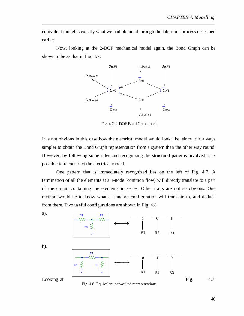
Now, looking at the 2-DOF mechanical model again, the Bond Graph can be
shown to be as that in Fig. 4.7.
:V1:V2
:f2
:f1
:M1:M2
:Spring1
:Spring2
:Damp1
:Damp2
:F1:F2
Fig. 4.7. 2-DOF Bond Graph model
It is not obvious in this case how the electrical model would look like, since it is always
simpler to obtain the Bond Graph representation from a system than the other way round.
However, by following some rules and recognizing the structural patterns involved, it is
possible to reconstruct the electrical model.
One pattern that is immediately recognized lies on the left of Fig. 4.7. A
termination of all the elements at a 1-node (common flow) will directly translate to a part
of the circuit containing the elements in series. Other traits are not so obvious. One
method would be to know what a standard configuration will translate to, and deduce
from there. Two useful configurations are shown in Fig. 4.8
a). 1 1 0
⎯→←R3 R2 R1
b).
Looking at Fig. 4.7,
0 0 1⎯→←
R2 R1 R3
Fig. 4.8. Equivalent networked representations
40
CHAPTER 4: Modelling ________________________________________________________________________
configuration (a) fits the bill. A common effort node (0) is in between two common flow
nodes (1). Putting things together, the equivalent 2-DOF model will be then as
represented in Fig. 4.9.
Fig. 4.9. Equivalent 2-DOF Electrical Model
The equivalent transfer function for such a circuitry is
[ ] [ ] [ ][ ] [ ] [ ] [ ] 11111111
21111
311
411
21
3
++++++++++++
=RCCRsRCCRLCCLCLsRCCRRCCLsLCLCs
CCsRCCsLCCsVI
Again, the transfer function is assigned some arbitrary values to show it is truly a 2-DOF
model.
C = C1 = 32.5 pf
R = R1 = 166 Ω
L = L1 = 0.29 mH
Fig. 4.10 shows the frequency response of such a system. As expected, the electrical
circuit possess two resonance peaks.
41

CHAPTER 4: Modelling ________________________________________________________________________
Fig. 4.10. Frequency response of obtained circuit
For more complicated structures, it is not a simple process to derive the electrical
parameters and thereby estimate the mechanical parameters of the structure. However, the
methodology has been demonstrated here, and it is a matter of application, depending on
the structure that is being modelled.
As a further example, Clark et al [23] had demonstrated 2-DOF resonating
structures. A simplified schematic is shown in Fig. 4.11 and the corresponding electrical
equivalent model is shown in Fig. 4.12. The structure is made up of two resonators
connected to each other through a beam (Fig. 4.11), modelled as a spring element.
Fig. 4.11. Schematic of coupled resonators
If damping is neglected for the connecting beam, it is simply modelled as a capacitor in
the electrical model (Fig. 4.12).
42

CHAPTER 4: Modelling ________________________________________________________________________
Fig. 4.12. Equivalent model for coupled resonators
4.6. Non-Linear Modelling
All the above modelling is only valid for linear elements. Unfortunately, as was
shown in the previous chapter, MEMS parallel plate devices exhibit non-linear
characteristics due to the V2 term in the force. Moreover, in cases where miniaturization
holds greater importance than easy detection, smaller devices means smaller capacitance
changes and therefore are more susceptible to parasitics. In such cases, the detection
scheme can rely on utilizing the characteristics of non-linearity to overcome the problem.
This is discussed in the next chapter.
43

CHAPTER 5: Device Characterization ________________________________________________________________________
CHAPTER 5: Device Characterization 5.1. Initial Characterization
As shown earlier in Chapter 3, a parametric amplification system requires the
device to be pumped at resonance to obtain maximum power transfer to the output. This
knowledge is also necessary to design the filters for the input and output signals.
However, the detection of resonance is not a straightforward process. As mentioned in the
previous chapter, the existence of parasitic capacitance at an order of magnitude higher
than the signal greatly complicates the detection.
As a result, it had been necessary to circumvent the problem through the use of
techniques such as Electrical Amplitude Modulation (EAM) [18] as well as 2f detection
[17]. However, these methods have a severe limitation: implementation is possible only
for two-port devices. Take, for example, the 2f technique applied to a resonator (Fig. 5.1).
Lock-in Amplifier
Current amplifier
mass
i
VAC
VDC
Fig. 5.1. Schematic for 2f resonance detection scheme
The excitation of the device is achieved through the pumping of an AC signal on
one side of the combs, with a DC voltage applied to the mass. As shown in Chapter 2,
such a configuration results in the device resonating at the frequency w of the AC as well
as at 2w. The other side of the comb is then connected to a current amplifier, which will
then be at virtual ground. A current, i(t) results at the comb due to the capacitance
variation and the presence of the DC voltage. Detection is done not at the pumping
44

CHAPTER 5: Device Characterization ________________________________________________________________________
frequency w but rather at 2w as the current due to parasitics occurs solely at w. Thus the
need for a lock-in amplifier to do the signal processing.
In summary, these methods require one port for actuation and the other port for
detection of the signal. Such schemes are not applicable for one-port devices. To the
author’s knowledge, there is no method which is suitable for one-port devices.
A simple alternative is proposed here: to send an AC signal into one side of the
plate only. The AC input will contribute in two ways: it actuates the one-port device as
well as modulates the detected signal. With just an AC, the actuation force occurs singly
at 2w only. In this chapter, a modified 2f detection, termed 3f detection, is presented and
analyzed. Before this 3f detection scheme is discussed, we first introduce an instrument
that is essential to this technique: a Lock-In amplifier.
5.2. Resonance Detection
Raskin et al. [12] detected resonance for their parallel plate device by applying AC
on top of a DC on one plate and a current amplifier to the other. The situation may be
represented as:
dcac VwtVtv ++= )sin()( 1φ
and
( ) ( )2210 2sinsin)( φφ ++++= wtCwtCCtC ww
We can show that there are effectively three frequencies which we can detect at. We know
that
[ ]dt
tdCtvdt
tdvtCtvtCdtdti )()()()()()()( +==
The current output at frequency w:
( ) ( )1220 cos21sin
21cos φφ +++− wtCwVwtCwVwtwVC wdcwacac
2w:
( ) ( )221 2cos22sin φφ +++ wtCwVwtCwV wdcwac
3w:
( )22 3sin23 φ+wtCwV wac
45

CHAPTER 5: Device Characterization ________________________________________________________________________
For Raskin et al, parasitic capacitance is not much of an issue as their capacitance
change for the membrane is in the order of 100-600 pf. With actuation force for a DC and
AC combination contributing to actuation frequencies at w as well as 2w, they could
detect resonance at w. Such a direct measurement is only possible if the capacitance
change is significantly larger (by an order of magnitude) than the amount of parasitics.
However, in our case, the aim is to demonstrate parametric amplification for small
capacitance devices. At such scale, the average device has only a few picofarads of
capacitance with capacitance change in the range of around tenths of picofarads. The
presence of parasitics at even 10 pf is sufficiently large to conceal the signal at w.
5.3. Lock-in Amplifier
The detection of resonance is not possible at the driving frequency but at higher
multiples of the input signal. To obtain the frequency response curve for such a system,
we use a lock-in amplifier with a current amplifier as our detection scheme.
Lock-in amplifiers are used to detect and measure very small AC signals. The
principle of operation is based essentially on the mathematical relation that
[ ]twwtwwAtwtwA )cos()cos(2
)sin()sin( 212121 +−−=
where w1 and w2 represents some arbitrary frequencies and A represents an arbitrary
constant which is the magnitude of the signal we want to detect.
If , then we see that the first term on the right reduces to a constant. This
constant contains the magnitude of the signal we are interested in. Thus, by sending the
resulting signal through a low pass filter to remove all frequency signals, we can obtain
the magnitude of the signal which would otherwise be overwhelmed by noise or stray
signals.
21 ww =
This simple mathematical relation results in a highly versatile instrument that
allows the user to either extract a signal within a very noisy environment or make high-
resolution measurements. The lock-in amplifier requires a reference signal to do the
internal multiplication. Typically, the device is excited at a certain frequency, and this
excitation can be external or from the lock-in amplifier itself. The output signal is fed into
the instrument and based on the reference (the external excitation or its own output
46

CHAPTER 5: Device Characterization ________________________________________________________________________
signal), internal processing is done to extract the signal occurring at that reference
frequency.
By repeating this process for a range of frequencies, and extracting the DC
component every time, we effectively get the frequency response of the device. The lock-
in amplifier basically sweeps through the frequency range and does an internal
multiplication of the received signal. The input signal is multiplied at the driving phase as
well as at 90° phase shift. So the user is able to plot frequency response curves at X (0°)
and Y (90°) against frequency as well as magnitude ( )22 YX + . The phase relation is
obtained through ⎟⎠⎞
⎜⎝⎛−
XY1tan at each frequency point.
The ‘quality’ of the extracted signal depends upon several factors, amongst which
is naturally the passband of the lowpass filter. The smaller the passband, the closer we get
to obtaining purely the DC signal. However, since the filters used are digital filters, it also
means that a longer sampling time is required for tighter passbands. For a digital lock-in
amplifier (which is what is being used), another factor would be the user-defined
sensitivity. Since the number of bits in the internal memory is fixed, by stating the value
of the maximum voltage that can be measured, the resolution of the readings is affected as
well. If the maximum voltage is stated too high, small fluctuations in the signal will not be
extracted. In essence, careful control of the various parameters in a lock-in amplifier has
to be observed to extract the embedded signal properly.
More detailed operation and characteristics of lock-in amplifiers can be found in
ref [17].
5.4. 3f Detection Scheme
The reference frequency that is multiplied internally by the lock-in amplifier need
not be at the driving frequency. It can also be at multiples of the driving frequency. That is
the basis of the 2f measurement technique. Parasitic capacitance only affects the signal at
the driving frequency and capacitance variation also occurs at two times the driving
frequency. Therefore, the frequency response of the device can be obtained by using the
lock-in amplifier to detect at twice the driving frequency.
47

CHAPTER 5: Device Characterization ________________________________________________________________________
Using a 3f measurement to detect resonance, we apply a single Vac to one side of
the device and the current amplifier to the mass. We now derive the exact output relation.
For an input of , the actuation force is affected by the term VwtVV ac sin= 2
( ) ( )wtVwtVV acac 2cos121sin 222 −==
To simplify our analysis later, we re-write the above equation as
wtwt 2cos2
2sin −=⎟⎠⎞
⎜⎝⎛ −
π , resulting in
⎟⎟⎠
⎞⎜⎜⎝
⎛⎟⎠⎞
⎜⎝⎛ −+=
22sin1
2122 πwtVV ac
From mechanical vibration, we know that for an excitation force of where
w
twFF dsin0=
d is the applied driving frequency, the resultant response is given by
( )φ−= twXx dsin
where 222
0
1 ⎟⎠⎞
⎜⎝⎛+⎟
⎟⎠
⎞⎜⎜⎝
⎛−
=
kcw
kmw
kF
Xdd
and
kmwk
cw
d
d
2
1tan
−
⎟⎠⎞
⎜⎝⎛
=φ
Similarly, the resultant capacitance change must approximately be of the form,
⎟⎠⎞
⎜⎝⎛ −−+= φπγ
22sin2)( 010 wtCCtC
where φ is a function of driving frequency and 2πφ = at resonance. (This is not exactly
true since the actuation force is actually non-linear, as it is a function of displacement as
well. However, it can be shown that the resultant excitation at w is sufficiently small to be
neglected). γ1, defined in this case, is the term that varies with the frequency and the Vac
applied to the device. Naturally, γ1 will be greatest at resonance for a given Vac.
48

CHAPTER 5: Device Characterization ________________________________________________________________________
Now, we want to see the current output phase relations. As usual, we use
dttdCtv
dttdvtCti )()()()()( +=
For this configuration, the resultant current output is
⎟⎠⎞
⎜⎝⎛ −−+⎟
⎠⎞
⎜⎝⎛ −−−= φπγφπγ
23sin3
2sincos)( 01010 wtVCwwtwVCwtwVCti acacac 5.1
Detecting resonance at 3f, we are effectively detecting the third term.
Therefore, the device is resonating at twice the driving frequency, but the detection
is done at thrice that frequency. The lock-in amplifier effectively plots the response curve
with the x-axis being the value of the driving frequency. So, to interpret the plot, i.e. to
obtain the actual frequency response of the device, one needs to multiply the x-axis by a
factor of 2.
Essentially, that single AC input into the device performs two functions. Firstly, it
actuates the device at twice the input frequency. Secondly, it performs an amplitude
modulation on the output signal at the same time. The relevant signal to be extracted then
exist at three times the input frequency.
Detecting resonance is not straightforward. There may be multiple little peaks due
to irregularities when the initial broad frequency sweep is done. The highest peak is
naturally taken to be resonance. However, the phase and X, Y plots allow us to verify
resonance with greater confidence.
For this 3f detection scheme, resonance is confirmed upon seeing an ‘inverted’
peak for X and a ‘S’ on its side for Y. Our interest is in the term
⎟⎠⎞
⎜⎝⎛ −− φπγ
23sin3 01 wtVCw ac . Vibration analysis tells us that
2πφ = , so the net phase
change in the signal is π− .
5.5. Extraction of γn coefficients
From the derivation of parametric amplification in Chapter 2, knowledge of the
various γn coefficients is necessary to estimate the characteristics of the parametric device.
In this section, we will discuss the means of extraction.
49
CHAPTER 5: Device Characterization ________________________________________________________________________
γn is effectively the value of the capacitance change ratio at the resonating
frequency. As such, there is no direct means of obtaining it. Some indirect method has to
be used. Since current is the most easily obtainable output which can be measured, it is
natural that it be examined first. Looking at
[ ]dt
tdCtvdt
tdvtCtvtCdtdti )()()()()()()( +== 5.2
a possible method of extracting the coefficients would be to obtain capacitance-time, C(t)
and then obtain the various coefficients by some means of fourier transform. Rearranging
(5.2) the capacitance time information can be obtained through
( )( )( )tv
dttitC ∫=
The capacitance change can be approximated to be,
( )∑ ++= nnn twCCtC φγ cos2)( 00
or
( ) ( ) ( )∑ ∑++= twtwCtC nnsnnc sin2cos20 γγ
taking as many terms as necessary. Knowing C(t), we can extract each of the coefficients.
Since ( ) baRbaRbaR sinsincoscoscos −=+ , to obtain γn and φ would then be
22nsncn γγγ +=
⎟⎟⎠
⎞⎜⎜⎝
⎛−= −
nc
ns
γγ
ϕ 1tan
However, this approach did not work out for two main reasons. Firstly, i(t) data
obtained from the oscilloscope are found to contain too much noise (Fig. 5.2). As a result,
the processed fluctuates too much. An example of the processed Q(t) is
shown in Fig. 5.3. There seems to be a bias in the current, which should not be due to the
purely sinusoidal input. This bias, attributed mostly to noise, explains why the Q(t) (Fig.
5.3) increases with time.
( ) ( )∫= dttitQ
50

CHAPTER 5: Device Characterization ________________________________________________________________________
Fig. 5.2. Plot of extracted noisy current against time
Fig. 5.3. Plot of processed Q(t)
Secondly, as only an AC signal is applied, there are values for which 0)( =tv .
This will result in situation where a division by zero needs to be done and therefore such a
method is not applicable.
51

CHAPTER 5: Device Characterization ________________________________________________________________________
This problem can be solved if the actuation port has a DC bias larger than the AC
signal, which would remove such zero potential points. However, a DC bias will shift the
equilibrium position of the device. The practical set up of a parametric amplification do
not actually require a DC bias applied to the system. Moreover, the bandpass filters
required in the set up will not allow the DC signal to reach the device. As such, this
operation to obtain γn is unrealistic since we may be able to extract γ1 at the end but at a
mode of operation unreflective of the actual final set up.
As a result, the problem has to be approached in another manner. Since we are
only concerned with the coefficients γn, we can avoid the impasse if we do not need to use
the full waveform of C(t). We know that current can be approximated by (5.1)
⎟⎠⎞
⎜⎝⎛ −−+⎟
⎠⎞
⎜⎝⎛ −−−= φπγφπγ
23sin3
2sincos)( 01010 wtVCwwtwVCwtwVCti acacac
The value of γn is actually contained in the coefficient of 3w. Thus, by extracting the
coefficients directly from the sampled i(t), we can obtain the value of γn.
5.5.1 Extraction method
Fourier analysis does not give the actual amplitude of the embedded signal of the
frequency. Instead, the magnitude shown is usually at some arbitrary scale, with the intent
of showing the ‘strength’ of the signal. Some modifications of the fourier transform would
thus be necessary to apply it in our case. Fig. 5.4. visualizes the operation.
Waveform
Sampled data
Fig. 5.4. Sample data multiplied by a sinusoidal waveform
The basis of fourier analysis lies in the fact that we can know the strength of the
signal at a certain frequency if we multiply it by a series of weights, which approximates a
sine or cosine wave. By summing the result for that frequency sampled, the larger the
52

CHAPTER 5: Device Characterization ________________________________________________________________________
value of the output the stronger the presence of that frequency. On the other hand, the sum
will be close to zero if the sample does not contain the frequency of the wave: the positive
values will approximately cancel out the negative values. If we were to vary the frequency
of the sine or cosine wave and multiply them with the sampled data, we effectively obtain
a plot or frequency spectrum showing the various strengths of the sampled data at
different frequencies.
Since the resulting value for a correlated frequency gets larger as the time sampled
increases, it also explains why resolution improves for longer sampling time for fourier
transform.
In our case then, the magnitude of the resultant summed weights cannot allowed to
be arbitrary. A sampled sine signal of, say, must give a result of a value 3. To do
that, we have to do some form of compensation to the weights.
wtsin3
It is perhaps easier to find the solution to the problem by looking at a perfectly
correlated sampled data of the function . Now, if the waveform used is also ,
the resulting summed value will be
wtsin wtsin
( )∑ 2sin wt . The exact value of depends
on two factors: the sampling rate (which will determine how many values are taken within
a period of time) and the sampling time. It is easily seen then that the higher or longer
either of these factors is, the greater the magnitude of the result.
(∑ 2sin wt )
The solution should now seem obvious: simply divide every waveform result by
its magnitude squared i.e. ( ( )∑ 2sin nwt ) to normalize the value to 1. Take for example
the case above. If the sampled data is of the function , the resultant summed
weights for a waveform of will be
wtsin3
wtsin (∑ )∑ =× 2sin3sinsin3 wtwtwt . Thus by
dividing the result by the squared sum of the waveform, ( )∑ 2sin wt , we extract the
magnitude 3.
So, by dividing the value obtained for a sampled sine wave of magnitude 1, we
will normalize the value to 1 and obtain the value of the coefficient exactly, i.e.
( )
( )∑∑ ×
= 2sin
sin
nwt
nwtcurrentnsγ 5.3
53

CHAPTER 5: Device Characterization ________________________________________________________________________
( )
( )∑∑ ×
= 2cos
cos
nwt
nwtcurrentncγ 5.4
As mentioned earlier, 22nsncn γγγ += .
After extracting acn VCw 013 γγ = , γ1 can be obtained by dividing by the various
terms in the expression. However, it must be acknowledged here that this method to
extract coefficients will result in approximate values.
5.6. Extracting Rc
It is necessary to obtain the internal resistance, Rc of the device. Rc will determine
the amount of internal losses of the device. Simply by applying a voltage across the
terminals and measuring the resulting output will not work in this case since we are
actually measuring a variable capacitor.
From the previous chapter, it is recognized that a resonating device can be
represented as a series LCR with a parasitic capacitance C0 in parallel. A model which
includes the internal resistance of the device, Rc, the equivalent circuit would be depicted
as in Fig. 5.5.
Fig. 5.5. Equivalent electrical model of device
The equivalent impedance can be derived from the circuit representation to be
( )
( )xxxxx
xxxxceff CLwCjwRjwCjwC
CLwCjwRRimp 2
0
2
11
−++−+
+= 5.5
Simply by observation, it can be seen that resonating the device at high frequencies will
result in the second term being equal to zero, thereby obtaining
ceff Rimp ≈
The internal resistance of the device can subsequently be determined.
54

CHAPTER 5: Device Characterization ________________________________________________________________________
In mechanical terms, driving the structure at frequencies beyond its natural
frequencies results in amplitudes of vibration approaching zero. The structure then
approaches a system of a fixed capacitor. The resistive parameter of the device is then
measurable.
55

CHAPTER 6: Filter Design ________________________________________________________________________
CHAPTER 6: Filter Design
6.1. Filter Design
Filter design is a very mature field [24], so not much discussion will be done here.
A general comparison of the performance of each type is given below [25]:
Butterworth: flat pass band, adequate roll-off, mathematically simpler
Chebyshev: steeper roll-off, greater pass-band ripple
Elliptic-function: equal-ripple variation in both passband and stopband
In this project, the aim is to verify parametric amplification in MEMS devices.
Though the use of transistors in the circuitry actually introduces additional shot noise into
the system, the noise analysis is not within the intended scope of the project. The use of
active filters will greatly simplify the design and testing of the circuitry since the load
does not have to be considered during the design of the filters.
6.1.1 Active filters
The design of active filters lies in the topology of the various ‘op-amps’,
capacitors and resistors. There are many configurations of such topologies, most of them
having second order transfer functions. The term ‘biquad’ refers to these configurations.
Knowing the final transfer function that is required, it is simply a matter of breaking down
the transfer function into various second order fractions, each of them realized using a
biquad and finally cascading them together to form the final filter.
A Kerwin-Huelsman-Newcomb (KHN) second order biquad was one of first such
designs based on the state-variable method. The circuit consists of three connected op
amps. The first implements a differential summer and the next two are inverting
integrators. Fig. 6.1 shows the circuit layout for the biquad.
56

CHAPTER 6: Filter Design ________________________________________________________________________
Differential summer Inverting integrator 1 Inverting integrator 2
Fig. 6.1. Schematic for a KHN biquad
Depending upon which output of the op-amp you tap out, you can realize a low-
pass, high-pass or band-pass filter: the output from the differential summer will result in a
high-pass filter, a band-pass filter if tapping from inverting integrator 1 and finally a low-
pass filter from inverting integrator 2.
The transfer function for a second order band-pass configuration can be derived
and shown as
( )
( )21521
6
151
652
151
654
0
CCRRRR
CRRRRRRR
ss
CRRRRRRR
s
VV
set
QG
set
Q
s ++
+
+
= 6.1
The filter characteristics that can be expressed are given below [33]
21215
42
CCRRRRwn = 6.2
( )21
225
114
5
4
3
1
1
⎟⎟⎠
⎞⎜⎜⎝
⎛
+
++
=CRRCRR
RR
RRRRR
Q QG
QG
6.3
57

CHAPTER 6: Filter Design ________________________________________________________________________
G
BP RR
gain 3= 6.4
This implementation is easily achieved through the use of Burr-Brown's UAF42
Universal Active Filter IC [32]. It is a 14-pin DIP (Dual Inline Package), which comprises
of four op-amps and certain fixed capacitance and resistance values. Three of the op-amps
are wired internally as a KHN biquad, with the last one separated from the rest of the
circuit to be used as an inverter or a tuned circuit. With Ω==== kRRRR G 50354 and
fixed internally in the IC, we have RpFCC 100021 == 1, R2 and RQ to vary to achieve
the desired characteristics. The pins layout is shown in Fig. 6.2. The IC requires two
power inputs, V+ and V-. The power supply required is about +15 V and –15 V
respectively. A ground connection is also required for the IC (pin 11).
8
9
10
11
12
13
14
7
6
5
4
3
2
1
Frequency Adj2Low-Pass Vo High-Pass VoVIN3
VIN2 VIN1 Auxiliary Op Amp, +In Ground Auxiliary Op Amp, -In V+
Auxiliary Op Amp, Vo V-
Bandpass Vo Frequency Adj1
Fig. 6.2. Schematic of pins layout
Design of the filter is then varying R1, R2 and RQ to suit the characteristics. Burr-
Brown provides a series of FilterProTM computer-aided design programs to guide the user
through the design process. The program contains a library of commercially available
resistance values. By designating the desired filter characteristics, the program searches
through its database and comes up with the resistor values which best matches the
performance required. A sample program screen is shown in Fig. 6.3.
58

CHAPTER 6: Filter Design ________________________________________________________________________
Fig. 6.3. Sample screen shot of FilterPro program
6.2. PCB Design
As noted earlier, the effect of parasitics poses problems in the detection of MEMS
devices. Imperfect connections, haphazard wiring all may result in contamination of the
signals. Thus, in the implementation, a generic PCB was designed instead of using normal
boards. This reduces the amount of soldering, connections and possible improper
connecting wiring. It was foreseen that the maximum number of cascaded stages of filters
is three, due to the fact that the greater the number of stages, the greater the amount of
insertion losses. The PCB was drawn using ProtelTM [31] and sent for fabrication at EDA
Singapore. The drawn PCB is shown in Fig. 6.4.
Power lines
connectors
pad
3 rows of fsocket
ilter s
Fig. 6.4. Drawing of PCB in Protel
59

CHAPTER 6: Filter Design ________________________________________________________________________
The PCB was designed to be as generic as possible. It is a two-layer board: the
lines in red at the top layer and the lines in blue the bottom layer. There are three rows of
ICs intended for the three filters that are required. Three lines of power are supplied to the
chips: one line for ground, another for +15V and the last for –15V, which are the
operating voltages of the ICs. Though not marked on the drawing, the ground wirings run
in between the +15 V and –15 V supply (the middle line of the three lines) to minimize
stray electric fields on the board. This is intended to reduce parasitics.
The pad on the right (Fig. 6.4) is meant for cases in which the device is not
packaged. The die can then be fixed there and connections wire-bonded to the connectors.
The 8-pin DIPs are included on the board to accommodate possible future generic
op-amp ICs.
60
CHAPTER 7: Experiment Results ________________________________________________________________________
CHAPTER 7: Experiment Results 7.1. Device Selection
The device to be used to verify parametric amplification is chosen based on
several criteria. From the theoretical result, we know the importance of the following:
• High resonant frequency
We know that the amplification factor depends largely on the frequency ratios for
an up-converter. So higher resonant frequencies for the device will result in greater gain.
At the same time, the required filter will not need a steep cut-off, reducing the order of the
design. To implement parametric amplifiers practically, the frequency of the signal to be
amplified may not be low, perhaps of the order of kHz or MHz. In this case, to get
substantial amplification, we will require the device to be operating at the MHz or GHz
range. All these issues constitute the necessity for high resonant frequency devices.
Among the parameters which affect effective impedances of the up-converter, the
operating frequencies and C0 has the greatest variation. Operating at high frequencies will
allow the effective input and output impedances to be low, which may or may not be a
necessity for the operation.
• High capacitance change, γn
In a similar fashion, the amplification depends practically on the amount of
capacitance change in the device. In the choice of the device to use, it is preferable that γn
can be varied substantially so that γn dependence can be demonstrated. Unfortunately,
there is no direct means of measuring γn.
• Low resistance
Naturally, it is favourable for the resistance of the device to be as small as possible
to minimize losses. On the other hand, in the application of degenerate amplification, the
presence of real losses in the device might be useful to stabilize the system.
• Low average capacitance, C0
C0 encompasses mainly parasitic capacitance as well as the average capacitance
value. We would want parasitics to be as low as possible as they affect the actual
operation of the device as well as hinder the accurate detection of signals.
61

CHAPTER 7: Experiment Results ________________________________________________________________________
In view of these selection criteria, the resonant frequency of the device was
decided to be of higher importance and the simplest to select. Among the various
accelerometers and gyroscopes tested that contain a parallel plate mechanism, a BARS
gyroscope [27] was finally chosen. Initial testing in air showed a resonance frequency at
~1800 Hz at the sensing side, which is the highest among the various devices available.
The results are shown in the next section.
Moreover, the amount of capacitance variation of the BARS gyroscope is large
with a range of ~0.2 pf, compared to other devices. Among the devices tested for
suitability were some MUMPs accelerometers and EG&G accelerometers. However, they
were found to be unsuitable for various reasons: low resonance frequency, trapped
charges, low pull-in voltage, etc.
7.1.1 BARS Gyroscope
Basically, the gyroscope comprises an actuation side and a sensing side. The
actuation combs consist of comb-drives for the purpose of providing a constant actuation
force. The sensing plates are parallel-plates, meant for larger capacitance variation and
therefore the side suitable for our use. Fig. 7.1 shows an SEM of the BARS gyroscope
used.
Mass
Actuation (Comb Drive)
Sensing (Parallel Plates)
Springs
Fig. 7.1. SEM of BARS gyroscope
62

CHAPTER 7: Experiment Results ________________________________________________________________________
The device is packaged on a 24-pin DIP (Dual Inline Package). The pins configuration is
shown in the Table 7.1.
e
7.2. 3f Detection results
The resonant frequen
The 3f detection scheme des
resonance is tested on both si
ports 10 and 18 are the two
shown in Fig. 7.2.
Port 10
Mass (Port 14)
Fig.
The graphs below show the r
done between port 10-14 as w
Table 7.1: Pins layout of devic
Name Pin Number
Ground 16
Mass 14
Actuating 1 20
Actuating 2 12
Sensing 1 18
Sensing 2 10
cy of the device is the first thing that must be determined.
cribed in Chapter 5 was used for this purpose. The device
des of the device. Port 14 of the device connects to the mass;
parallel plates. The schematic of the measurement setup is
Port 18
Current Amplifier
Lock-in Amplifier
7.2. Schematic of the 3f measurement setup
esults obtained at atmospheric pressure. Measurements were
ell as 18-14.
63

CHAPTER 7: Experiment Results ________________________________________________________________________
7.2.1 Results for port 10-14
The result is shown in Fig. 7.3. The characteristic of the 3f detection scheme is the
inverted peak for X and the slanted ‘S’ for Y, as seen in the plot. As mentioned in Chapter
5, section 5.4, the true frequency response of the device is two times what the x-axis
shows. In this case, since Y cuts at about 900 Hz, the resonance in air about 1800 Hz.
X, Y and Mag against Frequency (Port 10-14)
-4.0E-05
-3.0E-05
-2.0E-05
-1.0E-05
0.0E+00
1.0E-05
2.0E-05
3.0E-05
4.0E-05
500 600 700 800 900 1000 1100 1200 1300 1400 1500
Frequency (Hz)
Volta
ge (V
)
X Y Mag
Fig.7.3. 3f detection for port 10-14
7.2.2 Results for port 18-14
Fig. 7.4 shows the result for port 18-14. As expected, the resonance is also about
1800 Hz (after multiplying the x-axis frequency by two).
As can be seen, the resonance in air is about 1800 Hz. With that in mind, the
required filter for the pump will be one at half the resonance (because the excitation will
be at twice the pump frequency without a DC bias), i.e. one at 900 Hz.
64

CHAPTER 7: Experiment Results ________________________________________________________________________
X, Y and Mag against Frequency (Port 18-14)
-4.0E-05
-3.0E-05
-2.0E-05
-1.0E-05
0.0E+00
1.0E-05
2.0E-05
3.0E-05
4.0E-05
500 600 700 800 900 1000 1100 1200 1300 1400 1500
Frequency (Hz)
Volta
ge (V
)
X Y Mag
Fig.7.4. 3f detection for port 18-14
An up-converter output frequency is at the sum of the input and pump frequencies.
So if the signal is to be at about 300 Hz, a filter at 2100900300 =+ Hz will be required
for the implementation of an up-converter. The theoretical maximum gain possible is
1773002100
≈= dB.
We will only use port 10 and mass 14 for the implementation of the parametric
amplifier. The subsequent device parameters are also obtained with this configuration in
mind.
7.2.3 Vacuum chamber testing
To increase the amount of capacitance change at resonance, the rest of the testing
are done in a low pressure environment. A MMR vacuum chamber (Fig. 7.5) pumped till
about 6 mTorr, is used.
65

CHAPTER 7: Experiment Results ________________________________________________________________________
Fig. 7.5. Pictures of MMR Vacuum Probe station
The resonant frequency is again obtained at this pressure. The resonance of port
10-14 is shown in Fig. 7.6.
Plot of X, Y & Mag against Frequency (port 10-14)
-1.0E-05
-8.0E-06
-6.0E-06
-4.0E-06
-2.0E-06
0.0E+00
2.0E-06
4.0E-06
6.0E-06
8.0E-06
1.0E-05
1.2E-05
600 650 700 750 800 850 900 950 1000
F requency (H z)
X Y M ag
Fig. 7.6a. Frequency response from 600-1000 Hz
66

CHAPTER 7: Experiment Results ________________________________________________________________________
Plo t o f X , Y & M ag ag ainst F req uency ( Po rt 10 - 14 )
-1.5E-05
-1.0E-05
-5.0E-06
0.0E+00
5.0E-06
1.0E-05
1.5E-05
880 882 884 886 888 890 892 894 896 898 900
Fr e que nc y ( Hz )
X Y Mag
Fig. 7.6b Frequency response at 880-900 Hz
Comparing Fig. 7.6a to Fig. 7.3, the resonance peak is much sharper since it is
done in vacuum. Fig. 7.6b shows the frequency response as the scanning is done at higher
resolution (0.1 Hz). From Fig. 7.6b, we can see that the resonance frequency is about 888
Hz.
7.3. Device Parameters
7.3.1 Cp-D curve
The Capacitance-Dissipation curve is useful in determining various characteristics
of the device. It can show the response of the device to potential applied as well as the
pull-in voltage which the device fails. This can be obtained from the HP Impedance
Analyzer 4194A.
For a device which is functioning well, it should show a quadratic relationship
between capacitance and applied voltage (due to the fact that the resultant force on the
plates is dependent on V2). Naturally, the curve should then be symmetrical. The static
capacitance C0 can also be obtained here. The C-D curve is for the device is shown in Fig.
7.7.
67

CHAPTER 7: Experiment Results ________________________________________________________________________
Graph of Cp (f) & Dissipation against bias Voltage (V)
7.42E-127.44E-127.46E-127.48E-127.50E-127.52E-127.54E-127.56E-127.58E-127.60E-127.62E-127.64E-12
-2.0 -1.0 0.0 1.0 2.0
Voltage (V)
Cap
acita
nce
(f)
1.92E-02
1.93E-02
1.94E-02
1.95E-02
1.96E-02
1.97E-02
1.98E-02
1.99E-02
Dis
sipa
tion
Capacitance Dissipation
Fig. 7.7. C-V curve for port 10-14
From previous experience, the device snaps (the mass touches the plates) at
between 2-3 V. We then limit the C-D measurement to stop at ± 2 V. As seen from Fig.
7.7, the C-D curve shows good symmetry, demonstrating good electrostatic characteristic
of the device. Non-symmetrical curves often means that there are residue charges static on
the plates, which is often the cause of unexpected results during further testing. From the
curve, we can also approximate C0 = 7.5 pf.
7.3.2 Internal resistance, Rc
The means of obtaining the internal resistance of the device has been explored in
Chapter 5. Through the application of a high frequency voltage to the device, the
Impedance Analyzer is able to do measure resistances. For this case, the real and
imaginary components of impedance are obtained for various DC bias voltages. The
resulting curve is shown in Fig. 7.8.
68
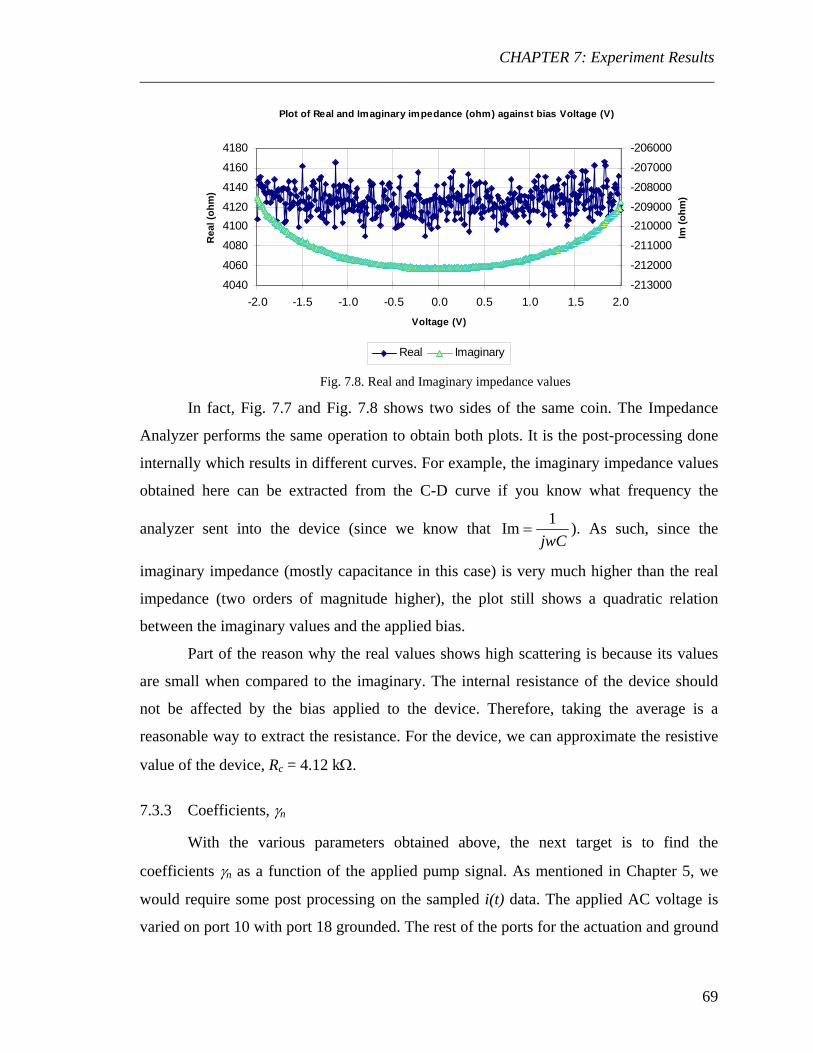
CHAPTER 7: Experiment Results ________________________________________________________________________
In fact, Fig. 7.7 and Fig. 7.8 shows two sides of the same coin. The Impedance
Analyzer performs the same operation to obtain both plots. It is the post-processing done
internally which results in different curves. For example, the imaginary impedance values
obtained here can be extracted from the C-D curve if you know what frequency the
analyzer sent into the device (since we know that jwC1Im = ). As such, since the
imaginary impedance (mostly capacitance in this case) is very much higher than the real
impedance (two orders of magnitude higher), the plot still shows a quadratic relation
between the imaginary values and the applied bias.
Part of the reason why the real values shows high scattering is because its values
are small when compared to the imaginary. The internal resistance of the device should
not be affected by the bias applied to the device. Therefore, taking the average is a
reasonable way to extract the resistance. For the device, we can approximate the resistive
value of the device, Rc = 4.12 kΩ.
Plot of Real and Imaginary impedance (ohm) against bias Voltage (V)
4040
4060
4080
41004120
4140
4160
4180
-2.0 -1.5 -1.0 -0.5 0.0 0.5 1.0 1.5 2.0
Voltage (V)
Rea
l (oh
m)
-213000
-212000
-211000
-210000-209000
-208000
-207000
-206000
Im (o
hm)
Real Imaginary
Fig. 7.8. Real and Imaginary impedance values
7.3.3 Coefficients, γn
With the various parameters obtained above, the next target is to find the
coefficients γn as a function of the applied pump signal. As mentioned in Chapter 5, we
would require some post processing on the sampled i(t) data. The applied AC voltage is
varied on port 10 with port 18 grounded. The rest of the ports for the actuation and ground
69

CHAPTER 7: Experiment Results ________________________________________________________________________
are all grounded as well. The mass is attached to the current amplifier as shown in Fig.
7.9.
Port 10
Port 18
Current Amplifier
Mass
Oscilloscope
Vac
Fig. 7.9. Schematic of setup to measure γ1
The output of the current amplifier is then fed into an oscilloscope. The output waveform
is then recorded.
The applied AC was varied from 0.3 V to 1.0 V (peak values). The 1.0 V limit is
chosen as a safety limit as resonance might result in the snap-in of the device. The current
data was sampled at 100 kHz in the oscilloscope. The extraction procedure is carried out
as described in the Chapter 5, section 5.5.
A summary of the extracted values is given in Table 7.2. The sampling rate from
the oscilloscope was 100 kHz, with a total sampling time of about 0.1s.
s
Table 7.2: List of extracted γ1 value
Vac (Peak) γ1
0.3 0.0018 0.4 0.0022 0.5 0.0024 0.6 0.0030 0.7 0.0042 0.8 0.0054 0.9 0.0066 1.0 0.0078
70

CHAPTER 7: Experiment Results ________________________________________________________________________
Plot of gamma against applied voltage (V)
00.0010.0020.0030.0040.0050.0060.0070.0080.009
0.2 0.4 0.6 0.8 1.0V o lt age ( V )
Fig. 7.10. Plot of extracted γ1 variation with voltage
Fig. 7.10 shows the value of γ1 increase as with applied actuation voltage, which is
expected. The apparent linearity from 0.5–1.0 V might suggest that setting the limit at 1.0
V might be too conservative (since we are expecting a quadratic relation). For protection
of the device however, we do not intend to push it too near its limit.
From the data, we see that the maximum γ1 we can achieve is not very high, at around
0.008.
The next step is to design the filters required. The knowledge of the resonance
frequency in section 7.2.3 has allowed the planning of the various bandpass filters
required.
7.4. Filter Design
Table 7.3 shows the theoretical values obtained from the FilterProTM program
required to achieve the filter characteristics. As exact matching of resistor values may not
be possible, some slight deviations from the desired values are inevitable. Two filters are
designed: one with the central frequency at 906 Hz, the other at 2.1 kHz. The passband
bandwidths are both at about 200 Hz.
The input signal at about 300 Hz that is to be magnified will be from a function
generator. As such, the source’s internal impedance (Rg) is fixed at 50 Ω, the standard
source impedance value for most instruments. Since the signal is from a function
generator, it should not carry too much stray signals. The 300Hz filter is therefore
71

CHAPTER 7: Experiment Results ________________________________________________________________________
designed purely as a tuned circuit, since not much attenuation of other frequencies will be
required.
T
R1
R2
First
stage
RQ
R1
R2
Second
stage
RQ
With each
series to obtain
attenuation require
In our case
has a passband of a
filters designed are
the bandpass at 90
Table 7.3: Theoretical and Practical values of resistors
906 Hz 2.1 kHz 300 Hzheoretical Practical Theoretical Practical Theoretical Practical
162.0 k 160 k 73.2 k 72.63 k 536 k 535.4 k
162.0 k 160 k 73.2 k 72.63 k 536 k 535.4 k
4.64 k 4.631k 1.82 k 2.0 k 49.9 k 49.9 k
191.0 k 192 k 78.7 k 78.92 k
191.0 k 192 k 78.7 k 78.92 k
4.64 k 4.631 k 1.82 k 2.0 k
biquad realizing a second order filter, we cascade several biquads in
either fourth order or sixth order filter depending on the roll-off
d.
, two fourth order filters using two stages each is designed. Each filter
bout 200 Hz. The theoretical frequency responses for the two bandpass
shown in Fig. 7.11 and 7.12. Fig. 7.11 shows the theoretical result for
6 Hz, Fig. 7.12 shows bandpass at 2.1 kHz.
Fig. 7.11. Bode plot for bandpass centered at 906 Hz72

CHAPTER 7: Experiment Results ________________________________________________________________________
7.4.1 Circuit Board design
A PCB board was de
noise due to poor connection
before the final design. The
7.13.
Capacitors of 0.1 farad are pl
to smoothen out any possible
IC chips
Fig. 7.12. Bode plot for bandpass at 2.1 kHz
signed for the filters so as to minimize possible sources of
s. Prior testing of the circuits on a breadboard is carried out
final board with the various connections is shown in Fig.
aced parallel between the power supply lines and the IC pins
power fluctuations from the source.
0.1 pf capacitors
Fig. 7.13. Assembled filters on PCB
73

CHAPTER 7: Experiment Results ________________________________________________________________________
The gain-phase results for the filters implemented on the PCB are shown in Fig. 7.13 and
Fig. 7.14. The gain-phase plots are obtained through the use of a HP 4194A Spectrum
Analyser.
Gain-Phase Plot
-50
-40
-30
-20
-10
0500 625 750 875 1000 1130 1250 1380 1500
Frequency (Hz)
Gai
n (d
B)
-200-150-100-50050100150200
Phas
e (d
eg)
Gain Phase
At the passband, there
designed. The attenuatio
kHz.
-80-70-60-50-40-30-20-10
01000 1250
Gai
n (d
B)
Fig. 7.14. Gain-phase for pass band at 906 Hz
is about -10dB of attenuation. The filter behaves exactly asn at high frequencies is significant, with already 30 dB at 1.5
Gain-Phase Plot
1500 1750 2000 2250 2500 2750 3000
Frequency (Hz)-200-150-100-50050100150200
Phas
e (d
eg)
Gain Phase
Fig. 7.15. Gain-phase for passband of 2.1 kHz
74

CHAPTER 7: Experiment Results ________________________________________________________________________
The passband attenuation in this case is about -7dB. The attenuation of lower
frequencies is also of interest here (to cut-off the pump signal). At 1 kHz, the attenuation
is also significant at about 40 dB.
7.5. Up-Converter Gain
With the foundation established, the next step is to incorporate everything to verify
parametric amplification for an up-converter device. Initially, attempts were made to
decouple the pump and signal by using the configuration shown in Fig. 7.16.
It was hoped that such a configuration would render the filters at the signal and
pump frequencies unnecessary, since the pump resonates the ‘top-to-mass’ gap of the
device, leaving the ‘bottom-to-mass’ gap for the mixing of charges when the signal
voltage is applied. This will be analogous to parametric amplification done by Rugar et al
[14] and Carr et al [13] where the use of optical detection removes the necessity for filters
altogether. The implementation of different energy domains ensures that the signals at
output are decoupled i.e. the actuation force is not picked up by the optical sensor.
However, attempts to detect signals using this configuration were unsuccessful.
No mixing of signals was detected, and no output at 2.1 kHz was observed. The success
of this configuration lies on the assumption that the signal can produce mixing due to
capacitance change at the ‘bottom-to-mass’ gap only. In practice however, mixing should
also occur at the ‘top-to-mass’ gap, since there is capacitance change there as well.
Another possible reason is that by applying two different frequencies at two locations (one
to the top plate and another to the mass), the resulting structure may not be resonating at
Top-to-mass capacitance
Vsignal
Vpump
Bottom-to-mass capacitance
Mass
Oscilloscope
Fig. 7.16. Originally intended configuration
75

CHAPTER 7: Experiment Results ________________________________________________________________________
the frequency assumed, i.e. at 1.8 kHz. Thus the resulting mixing cannot be detected at 2.1
kHz.
An alternative and simpler method is then used. The setup of the experiment is
shown in Fig. 7.17. The signal and pump sources are from a Yokogawa FG 300
Synthesized Function Generator. The detection can be either a Yokogawa DL1520 Digital
Oscilloscope or a HP 89410A Vector Signal Analyzer (VSA), depending on the
sensitivity required.
The signal and pump frequencies are supplied from the same function generator,
with a fixed source impedance of 50 Ω. All the signals and outputs are tapped from port
10 of the package. The mass, actuating combs and port 18 are all grounded. To minimise
problems and compensations required when using probe tips [30], output at the load is fed
directly into a current amplifier before sending into the VSA. The only inconvenience in
this case is that an additional step is required to compensate for the current gain. This is
considered minor compared to compensating for the probe impedance when measuring
potentials across high resistance (up to 1 MΩ in our case).
FG 300 Function Generator
Vector Signal Analyzer Agilent 89410A
Current amplifier load
fp + fsfs
fp
Fig. 7.17. Schematic of experimental setup
76

CHAPTER 7: Experiment Results ________________________________________________________________________
As a side note, it is found that the presence of the filters is imperative, as assumed
by theory. Without any one of the filters (for example connecting the pump directly to
port 10), no mixing of frequencies occurs and no output at 2.1 kHz is detected.
We first look the impedance characteristic of the device. From Chapter 3, it was
derived that
3
231
2
Tin RCww
R γ= 3.28
1
231
2
Tout RCww
R γ= 3.29
The effective output impedance of the device depends on the input source impedance,
which in our case does not change much since the source impedance is fixed at 50 Ω. It is
simply then
cgT RRR +≈1
4170412050 =+≈ Ω
The tabulated values of output impedance for the various γ1 values are shown in Table
7.4.
e
The operating frequ
324221 ×== fw ππ
88823 =×= Hzw π
5.70 =C pf
Table 7.4: Output impedance for different pump voltag
Vac (V) γ1 Rout (Ω) 0.3 0.0018 536,0000.4 0.0022 801,0000.5 0.0024 954,0000.6 0.0030 1,490,0000.7 0.0042 2,921,0000.8 0.0054 4,830,0000.9 0.0066 7,215,0001.0 0.0078 10,077,000
encies and C0 are those obtained from the device.
7.2034=Hz rad/s
13188 rad/s
77

CHAPTER 7: Experiment Results ________________________________________________________________________
By varying the pump voltage, the effective output impedance of the device can be
changed from 500 kΩ to 10 MΩ. This is a very wide range of impedance change, for an
input change of only 0.3-1.0 V.
On the other hand, the effective input impedance of the device depends on RT3,
which depends largely on the load. As an example of the characteristic, we look at the
variation for the case in which VVac 1= , and varying the load. The other parameters are as
above. The tabulated values for selected load resistances are shown in Table 7.5.
Table 7.5: Input impedances for fixed pump voltage
Load (Ω) γ1 RT3 (Ω) Rin (Ω) 50 0.0078 4,170 9,666,000
511 0.0078 4,631 8,704,0001000 0.0078 5,120 7,873,0004990 0.0078 9,110 4,425,000
10000 0.0078 14,120 2,855,00049900 0.0078 54,020 746,000
150000 0.0078 154,120 262,000249000 0.0078 253,120 159,000511000 0.0078 515,120 78,000
1000000 0.0078 1,004,120 40,000
The resistance values chosen are those physically available and attempted to cover as
wide range as possible.
The implication of this variation of effective output and input impedance of the
device is that the parametric amplifier can be made to act as a buffer between a low
impedance source and a high impedance load or vice versa. The aim then is to maximize
power transfer even though the system itself has mismatch source and load impedance
values. This is achieved by varying the amount of pump signal and, if possible, varying
the value of C0 through the application of a DC bias to the device.
To verify the excitation involved, only the pump signal at 888 Hz is turned on and
the output current is measured. As expected, only a current at 1776 Hz (2w) is detected
(Fig. 7.18). There is another smaller signal of 2664 Hz (3w) that is due to the non-linear
excitation as mentioned in Chapter 2.
78

CHAPTER 7: Experiment Results ________________________________________________________________________
Fig. 7.18. Plot when only pump signal is sent in
Next, both pump (888 Hz) and signal (324 Hz) are sent into the device. The results
shown next in Fig. 7.19 is a sample done for a load at 4.99 kΩ. To demonstrate that the
output signal is truly dependent on the frequencies of the two sources and not some noise
or arbitrary signal present, the signal is changed to 350 Hz. What can be observed in the
VSA is a shift in the various signals present. This change is shown in the Fig. 7.19 (in
red). All the various signals are permutations of the pump and signal frequencies. Their
relations are shown as well. The arrows shows the shift observed in the signal.
79Fig. 7.19. Plot showing the shift in frequencies

CHAPTER 7: Experiment Results ________________________________________________________________________
The various frequencies’ configuration (in blue) apparent are shown below:
21002 =+ sp ff Hz
201623 =− sp ff Hz
23402 =− sp ff Hz
225644 =−+ sp ff Hz
As a digression, from looking at the shift, one might be tempted to question the
outcome if the two largest peaks are brought together i.e. the input frequency required to
make . This works out tospsp ffff 232 −=+ 296=sf Hz, resulting in an output at 2072
Hz as shown in Fig. 7.20 (in red).
Fig. 7.20. Plot showing output for 296 Hz
The converged signal shows a signal strength which is in between that of
and alone. No analysis has been done at this present moment to
explain why the signal at 296Hz is not the sum of the two converged signals. One aspect
of the signals not shown on the plots is their actual phases. One possible reason for the
loss in signal strength is that
sp ff 23 − sp ff +2
sp ff 23 − and sp ff +2 are not coherent, i.e. there is a phase
80

CHAPTER 7: Experiment Results ________________________________________________________________________
difference between them. This special situation aside, the phase of the output signal is
inconsequential since we are only interested in the magnitude gain of the signals involved.
Having demonstrated that the signals are truly the resultant of mixing of signals
within the MEMS device, the approach is applied to non-degenerate amplification. Two
aspects will be verified: the relation between gain and load, Rl and the relation between
gain and γ1.
7.5.1 Gain-Load & Gain-γ1 Relationships
To obtain these two relationships, two terms are varied: the pump voltage, Vpump
and the load, Rl. Varying Vpump effectively changes the γ1 based on the extracted values
obtained earlier. However, additional compensation for the insertion loss of the filter has
to be taken into account. For example, input at 888 Hz of 5.0 Vpp has a loss of about 9
dBV, which results in the actual voltage being about 1.0 Vpeak.
The pump voltage is varied from 5.0 Vpp to 1.5 Vpp in steps of 0.5 Vpp. This
practically covers the range of γ1 that had been extracted previously. The corresponding
γ1’s are estimated through a linear interpolation from the results obtained.
The concept of gain might be subjective. Certain works define gain in forms like
the increase in signal strength after subjecting the system to the pump voltage [13]. This
method of defining gain can be confusing but in general yields much higher gain. Carr et
al [13] quoted gains of about 30 dB. This is due to the fact that without the pump, the
output frequency signal is very small, practically near the noise floor. The application of
the pump signal results in the output frequency becoming prominent, thus the huge gain
calculated.
However, in our case, the gain is defined as a measurement of power gain over the
available power from the signal, as per derived in Chapter 3. This is because our focus is
on the amount of power transfer from the input to the output frequency.
Table 7.6. summarizes the obtained values. All the values are in dB.
81

CHAPTER 7: Experiment Results ________________________________________________________________________
1.5 2.0 2.5 3.0 3.5 4.0 4.5 5.0 Ω γ1=0.19e-2 0.23e-2 0.26e-2 0.31e-2 0.48e-2 0.61e-2 0.74e-2 0.78e-2
1000 -114.5 -107.2 -102.5 -101.2 -90.8 -125.5 -129.2 -126.54990 -101.2 -92.9 -87.3 -84.5 -88.2 -108.5 -112.2 -109.3
10000 -95.3 -87.1 -81.8 -79.0 -86.8 -103.0 -106.2 -103.449900 -109.3 -101.3 -96.2 -93.1 -91.1 -89.0 -92.3 -89.966500 -111.9 -103.9 -98.9 -95.7 -93.7 -91.6 -89.9 -87.8
107000 -116.2 -108.0 -102.9 -100.0 -97.7 -96.3 -94.3 -92.6150000 -118.7 -109.9 -104.0 -100.3 -97.2 -94.9 -92.7 -91.3221000 -121.7 -113.2 -107.5 -103.6 -101.4 -99.4 -96.9 -95.7249000 -122.8 -114.0 -108.6 -104.7 -102.6 -100.5 -98.3 -96.9511000 -129.1 -120.5 -114.6 -111.0 -108.5 -106.4 -104.5 -103.0
1000000 -134.1 -126.3 -120.4 -116.5 -114.1 -112.0 -109.8 -108.3
Vpp
A comparison between the theoretical and experimental results for the case of 5.0 Vpp is
shown below in Fig. 7.21
Plot of Gain (dB) against Load (ohm)
-140
-130
-120
-110
-100
-90
-80
-70
-60
-50
-400 100000 200000 300000 400000 500000 600000 700000 800000 900000 1000000
Load (ohm)
Gai
n (d
B)
Theory Expt
There
kΩ is now ap
Moreover, the
a maximum o
possible, abo
Fig. 7.21. Plot comparing theoretical and experimental values for 5.0 Vpp.
are a couple
parent. At su
amount of ca
f 0.0078. Bot
ut –50 dB in
Table 7.6: List of gain obtained in dB
of issues here. Firstly, the effect of a device resistance of 4.12
ch high resistances, too much power is lost within the device.
pacitance variation (γ1) is too low, with a comfortable value at
h of these factors contribute to the amount of theoretical gain
this case. As a comparison, Raskin et al [12] used a huge
82

CHAPTER 7: Experiment Results ________________________________________________________________________
membrane which has internal losses of only 140 Ω and is capable of achieving 2.01 =γ .
In contrast, they were able to achieve gain of about 9dB.
Comparing our experimental and theoretical results then, there is consistently
about 40-50 dB differences in gain, even for other pump voltages. Besides the fact that
there may be other losses unaccounted for in the circuit, the nature of the filters used is a
contributory factor as well. The use of active filters instead of passive filters solved the
issue of having to design different filters: two for every point on the table (one for the
signal and the other for the output). That would have constituted about 176 filter designs
simply to match the filter characteristics needed.
However, active filters introduced another issue by itself. Solid state electronic
devices do not have the characteristic of achieving maximum power transfer. Instead, it
achieves maximum voltage transfer [31]. This is most likely the reason for the amount of
losses within the circuitry.
Nevertheless, the resistive value that maximizes gain can be approximated from
the theoretical values, given the limited number of resistor points available. A comparison
is shown in Fig. 7.22.
Plot showing optimal load (ohm) against gamma
0
10000
20000
30000
40000
50000
60000
70000
80000
0.000 0.001 0.002 0.003 0.004 0.005 0.006 0.007 0.008 0.009
Load
(ohm
)
Theory
Expt
n
Fig. 7.21 shows
the impedance that resu
this case, some form of
that the theory predicts
gamma
Fig. 7.22. Predicted and experimental optimal gai
a characteristic which is unique for parametric amplifiers, where
lts in maximum power transfer can be varied by another signal. In
tuning is achieved by varying the pump voltage. Fig. 7.21 shows
the optimal load very well, except for the case where 0048.01 =γ .
83

CHAPTER 7: Experiment Results ________________________________________________________________________
That is because the resolution of the load resistances used is not high: there is no
resistance used between 49.9 kΩ and 10 kΩ. Either of these values would not have fitted
the curve.
The dependence of gain on γ1 is shown in Fig. 7.23. It is simply plotted for various
constant loads.
Plot of Gain (dB) against the gamma for a given load
-140.0
-135.0
-130.0
-125.0
-120.0
-115.0
-110.0
-105.0
-100.0
-95.0
-90.00.0010 0.0020 0.0030 0.0040 0.0050 0.0060 0.0070 0.0080 0.0090
gamma
Gai
n (d
B)
1 meg 511 k 249 k 221 k 150 k 107 k
Fig. 7.23. Gain dependence on γ1
As expected, the gain for a given load increases as γ1 is increased. Though at loads
lower than 107 kΩ, the relation of the gain starts to become erratic. At the present
moment, the only plausible reason is because of the use of active filters instead of passive
ones.
84

CHAPTER 8: Conclusion ________________________________________________________________________
CHAPTER 8: Conclusion
As with all systems, the implementation of a parametric amplification system is
not straightforward. Several issues and unknowns have to be resolved. As a first step
towards understanding the system, the theoretical derivation is adapted to suit MEMS
devices. With the theoretical background established, the necessary ingredients to
implement a parametric amplifier become clearer.
Firstly, the device has to be appropriate. The resonance frequency and capacitance
change has to be high, with low internal resistance and parasitic capacitance. The last two
factors are not easily designed, being a function of process and careful placement of
electronics. However, the first two factors are easier to control through the design of the
structure. In this project, no optimized device was fabricated since the aim is to verify the
possibility of parametric dependence for the output signal. With the numerous devices
available in our laboratory, a BARS gyroscope was the device of choice due to its high
resonance frequency (compared to the other devices available) as well as its stable
capacitance variation.
Parametric amplification requires the various signals to be contained within their
individual loops, with mixing only occurring within the device itself. To achieve this,
filters were designed and implemented for each of the loops. This is necessary since we
are working totally in the electrical domain, unlike other works where different energy
domains were used for actuation and detection. An initial configuration for the device was
proposed that might have removed the need for filters. However, that configuration did
not achieve the objective and a simplified version was used instead.
As there is no direct means of measuring the amount of capacitance change (γn) in
the device during actuation, a method is proposed to extract this value from the current
signals. This parameter is important in the analysis of parametric amplification.
In the process of the implementation and characterization of the system, two
methodologies are proposed. Firstly, a 3f detection scheme is proposed which allows the
detection of one-port devices previously unattainable by other methods. The influence of
parasitic capacitance makes the detection of resonance difficult. Methods such as EAM
and 2f detection normally used to circumvent this problem, are only applicable to 2-port
85

CHAPTER 8: Conclusion ________________________________________________________________________
devices. This 3f method removes that restriction. Analysis and demonstration of the
method is shown and it permitted the detection of resonance effectively.
A means of obtaining the equivalent electrical model of mechanical systems is
proposed through the use of Bond Graphs. Such a scheme might be useful in extracting
mechanical parameters from the analysis of the electrical signals. Such a method had
already been demonstrated for single degree-of-freedom systems. What is proposed here
is a way to extend that capability to higher DOFs.
Finally, the cumulative work are all integrated into the analysis and test of a
parametric up-converter. The gain of the system is shown to be dependent on both γ1 and
load resistance, as predicted by theory. Though more losses within the circuit were
measured than predicted, the general response of the system agreed with theory,
especially the prediction of the load that gives optimal gain.
8.1. Future work
The interest in parametric amplification lies in its theoretical capability to achieve
low-noise amplification. As such, noise analysis would be a very interesting aspect.
Active filters cannot be used in this case, since the introduction of transistors introduces
more noise. The implementation of the system has to be well planned as its load
influences the filter characteristic of passive filters. A complete experimental programme
to analyze and compare the noise figure of such parametric amplification at high
temperatures with transistor based circuitry is suggested.
In order to fully exploit the gain of the amplification, the device that is being used
should be optimized for high frequency resonance as well as large capacitance change.
It may also be interesting to explore alternative forms of parametric amplification
configurations, for example the degenerate amplifier.
86

REFERENCES ________________________________________________________________________
REFERENCES 1. J.M. Manley and H. E. Rowe, “Some general properties of nonlinear elements –
Part1: General energy relations,” Proc. of the IRE, pp.904-914, July 1956
2. H. E. Rowe, “Some general properties of nonlinear elements—Part 2: Small
signal theory,” Proc. of the IRE, pp.850-860, May 1958
3. Uenohara, M., and Bakanowski, A.E, “Low-noise Parametric Amplifier Using
Germanium p-n Junction Diode at 6 kmc”, Proc. IRE, vol. 47, pp. 2113-2114,
December 1959
4. Michel Marhic, Frank Yang, Min-Chen Ho & Leonid G. Kazovsky, “High Non-
linearity Fiber Optical Parametric Amplifier with Periodic Dispersion
Compensation”, Journal of Lightwave Tech, Feb 1999, Vol.17, no.2, 210-215
5. M.L.Bortz, M.A. Arbore & M.M. Fejer, “Quasi-phase-matched optical parametric
amplification and oscillation in periodically poled LiNbO3 waveguides”, Optics
Letters, Jan 1 1995, vol.20, no.1
6. Nyquist, H, “Thermal agitation of electric charge in conductors”, Physical
Review, vol.32, pp.110-113, July 1928
7. J. Engberg & T. Larsen, Noise Theory of Linear and Nonlinear Circuits, John
Wiley & Sons, 1995
8. Boris A. Kalinkos, Nikolai G. Kovshikov, Mikhail P.Kostylev, “Parametric
Frequency Conversion with Amplification of a Weak Spin Wave in a Ferrite
Film”, IEEE. Trans. On Magnetics, Vol.34 P. 1393-1395 (1998)
9. Per. K. Rekdal & Bo-Sture K. Skagerstam, “Quantum Dynamics of Non-
Degenerate Parametric Amplification”, Physica Scripta. Vol.61, 296-306, 2000
87

REFERENCES ________________________________________________________________________
10. B. Yurke, M.L. Roukes, R. Movshovich and A.N. Pargellis, “A low-noise series-
array Josephson junction parametric amplifier”, Applied Phys. Lett. 69 (20), Nov
1996
11. A.Dana, F Ho & Y. Yamamoto, “Mechanical parametric amplification in
piezoresistive gallium arsenide microcantilevers”, Applied Phys. Lett. 72 (10),
March 1998
12. Jean-Pierre Raskin, Andrew R. Brown, Butrus T. Khuri_Yakub & Gabriel M.
Rebeiz, “A Novel Parametric-Effect MEMs Amplifier,” JMEMs, Vol.9, No.4, Dec
2000
13. Dustin Carr, Stephane Evoy, Lidija Sekaric, H.G. Craighead and J.M. Parpia,
“Parametric amplification in a torsional microresonator”, Appl. Phys. Lett. 77
(10), Sept 2000
14. D. Rugar & P. Grutter, “Mechanical Parametric Amplifier and Thermomechanical
Noise Squeezing”, Physical Rev Lett. Vol.67, no.6 Aug 1991
15. A. Olkhovets, D Carr, J.M.Parpia & H.G. Craighead “Parametric amplification in
nanomechanical resonators”, IEEE MEMS-2001 proceedings, January 2001
16. M. Zalalutdinov, A. Zehnder, A. Olkhovets, S. Turner, L. Sekaric, B. Ilic, D.
Czaplewski, J. M. Parpia and H. G. Craighead, “Auto-Parametric Optical Drive
For Micromechanical Oscillators”, Appl. Phys. Lett. 2000
17. Chan Mei Lin, Dynamic and Static Characterization of Microfabricated
Resonating Structures, Masters Thesis, National University of Singapore, 2002
88

REFERENCES ________________________________________________________________________
18. J. Cao & C.T.C Nguyen, “Drive Amplitude Dependence of Micromechanical
Resonator Series Motional Resistance”, Dig. Of Tech.Papers, 10th Int. Conf. On
Solid-State Sensors and Actuators, Jun 1999, pp. 1826-1829
19. William Tang, Electrostatic Comb Drive for Resonant Sensor and Actuator
Applications, Phd Thesis, University of California at Berkeley
20. L Blackwell, K Kotzebue, Semiconductor-Diode Parametric Amplifiers, Prentice-
Hall
21. Karnopp, Margolis, Rosenberg, System Dynamics: A Unified Approach, Wiley-
InterScience Publication, 1990
22. C.T. Nyugen, Ph.D. Dissertation, 1994, UC Berkeley
23. Clark T.C Nguyen, “Micromechanical filters for miniaturized low-power
communications”, Proc. Of SPIE: Smart Structures and Materials, 1999
24. Kendall L. Su., Analog Filters, Chapman & Hall, 1996
25. Simon Haykin, Modern Filters, Macmillan, 1989
26. V.J. Logeeswaran, M.L. Chan, E.H. Tay, F.S.Chau & Y.C. Liang, “A 2f method
for the measurement of resonant frequency and Q-factor of micromechanical
transducers”, Proc. SPIE Vol. 4755, DTIP 2002, Cannes pp.584-593
27. Chua Bee Lee, “ADA Framwork and its application to the development of MEMs
devices,” M.Eng. Thesis, National University of Singapore, 2001
28. J C Decroly, L Laurent, J C Lienard, G Marechal & J Vorobeitchik, Parametric
Amplifiers, Macmillan, 1973
29. Douglas C. Smith, High Frequency Measurements and Noise in Electronic
Circuits, Van Nostrand Reinhold, 1993
89

REFERENCES ________________________________________________________________________
30. Dennis Bohn, Unity Gain & Impedance Matching: Strange Bedfellows, Rane
Corporation, RaneNote 124
31. http://www.protel.com
32. http://www.ti.com
33. Burr-Brown® Application Bulletin (Filter Design Program for the UAF42
Universal Active Filter)
90

APPENDIX A ________________________________________________________________________
APPENDIX A Bond Graphs
Glossary of Terms:
• Ports: connections between subsystems which allow power to flow between them
• Multiports: subsystems with one or more ports
Concepts:
• All power variables are either effort e(t) or flow f(t)
• Energy variables momentum p(t) and displacement q(t)
•
( ) ( ) ( )
( ) ( ) ( )∫ ∫
∫ ∫
+==
+==
t
t
t
t
dttfqdttftq
dttepdttetp
0
0
0
0
• Efforts are placed above or to the left of port lines
• Flows are placed below or to the right of port lines
• Half arrow indicates the direction of power flow at any instant of time
• Full arrow indicates an active bond, or a signal flow at very low or no power
• Causal stroke: short, perpendicular line which indicates direction of the effort signal
• Effort and flow signal flow in opposite directions
Basic Component Models:
1-port elements
• Resistance--------- R
• Capacitor---------- C
• Inertia-------------- I
• Effort source------ Se
A1

APPENDIX A ________________________________________________________________________
• Flow source------- Sf
2-port elements
• Transformer------- TR
o Modulated transformer--- MTR
• Gyrator-------------GR
o Modulated gyrator-------- MGR
3-port elements
• Flow junction, 0-junction or common effort junction
• Effort junction, 1-junction or common flow junction
A2