parameter controls for enhanced peak-to-valley current
TRANSCRIPT

Supporting Information
Parameter Controls for Enhanced Peak-to-Valley Current
Ratio in MoS2/MoTe2 van der Waals Heterostructure
Ngoc T. Duonga,b, Seungho Banga,b, Seung Mi Leec, Dang X. Danga,b, Dong H. Keumb, Juchan
Leeb, Mun S. Jeonga,b,*and Seong C. Lima,b,*
a Department of Energy Science, Sungkyunkwan University, Suwon 16419, Republic of Korea
b Center for Integrated Nanostructure Physics, Institute of Basic Science (IBS), Sungkyunkwan
University, Suwon 16419, Republic of Korea
c Korea Research Institute of Standards and Science (KRISS), Deajeon 34113, Republic of Korea
* Address correspondence to [email protected] or [email protected]
Electronic Supplementary Material (ESI) for Nanoscale.This journal is © The Royal Society of Chemistry 2018

1. Optical images of MoTe2 and MoS2 flakes and the MoS2/MoTe2/hBN heterostructure.
Figures S1 (a) and (b) are optical images of the exfoliated MoTe2 and MoS2 flakes on poly vinyl-
alcohol (PVA)/ poly methyl methacrylate (PMMA) spin coated on the Si/SiO2 substrate. First,
MoTe2 and MoS2 flakes were exfoliated on the PVA/PMMA substrate and the h-BN flake was
exfoliated on the Si/SiO2 substrate. After dissolving PVA by water, MoS2 and MoTe2 flakes
remained on the surface of the PMMA sheet. Then, MoTe2 and MoS2 flakes were transferred on
the top of h-BN flake.
2. Raman mapping of the peak positions of the A1g and E2g modes of the MoS2 flake.
Scanning Raman spectroscopy of our sample was performed using NT-MDT (NTEGRA Spectra)
over the overlapped and pristine area of MoS2. Figure S2(a) is an optical image of the area to be
examined using the instrument. The peak position of A1g and E2g modes were monitored inside the
scanning area. The E2g mode of the overlapped MoS2 shows a redshift of ~ 1 cm−1 (from 381 cm−1
to 380 cm−1) compared with the pristine one; this can be attributed to the strain effect of MoS2 due
to the interaction with the underlying MoTe2 layer (Figure S2 (b)). The redshift of the E2g mode
by ~ 1 cm−1 indicates that the strain level exerted on MoS2 is up to 1 %. The same analysis is
applied on A1g mode. A mapping image of the A1g mode in Figure S2(c) demonstrates a redshift
Fig. S1. (a) MoTe2 and (b) MoS2 flakes are mechanically exfoliated on a PVA/PMMA coating
substrate. (c) MoTe2 and MoS2 heterostructure on a h-BN passivating layer.

by ~ 1 cm−1 (406.6 cm−1 to 405.7 cm−1), which can be attributed to the effect of electron transfer
from the MoTe2 to the MoS2 layer. 1
In addition to Raman peak analysis, the effect of strain is examined again using PL spectra. A
room temperature photoluminescence (PL) spectrum is obtained in MoS2 overlapped with MoTe2
using NTMDT-NTEGRA system that is equipped with 532 nm wavelength laser. In the Fig. S2
(d), a significant redshift, approximately 30 meV, in the spectrum is observed, which strongly
supports that MoS2 is locally strained due to MoTe2. The redshift of the A exciton peak by ~1 cm-
1 results from the strain level of MoS2 approximately 1 %.1-3
Figure S2. (a) MoS2/MoTe2 heterostructure with the scanning area. (b) E2g and (c) A1g Raman
peak positions for the pristine and overlapped MoS2 and MoTe2 regions, respectively. (d)
Arbitrary units PL spectra of pristine and overlapped MoS2.

3. I–V characteristics of the MoTe2 flake before and after BV doping.
We examined SiO2 protection layer for MoTe2 by BV using AFM. As shown in Fig. S3(a), SiO2
covers uniformly MoTe2 with the thickness of 100 nm. Hence, no direct doping of MoTe2 by BV
is expected to happen. However, a slight reduction of channel current is seen from the Ids-Vgs curve
in Fig. S3(b). In addition to it, a similar current decrease of channel current is also observed from
Ids-Vds curves in Fig. S3(c) and S3(d). But, the overall linearity in the Ids-Vds in Figs. S3 (c) and
S3(d) does not change. Hence, we expect that the current reduction in the figure is not because of
doping of MoTe2 by BV, but because of the dielectric properties of SiO2 and BV, whose dielectric
properties are quite different from the air. It is known that I-V properties are influenced by
Figure S3. (a) Thickness profile of SiO2 (b) Ids–Vgs of the MoTe2 flake after and before BV
treatment. Ids–Vds of pristine MoTe2 (c) after and (d) before BV treatment.

surrounding dielectric constant.4 If the doping of MoTe2 by BV occurred, then the p-type behavior
of MoTe2 would not be sustained after the BV doping that is a strong n-doping agent.
4. Temperature-dependence electrical characteristics of MoS2/MoTe2 heterostructure.
To further investigate the electrical transport in the doped MoS2/MoTe2 vertically stacked p-n
diodes, we measured the temperature-dependent electrical properties, Ids–Vds. Figure S4a shows
the I–V characteristics of the device in the temperature range of 60–300 K at Vgs = 0 V. All I–V
curves show a rectifying behavior where the current range increases as a function of temperature
in Fig. S4 (a) (shown in the semi-log plot in the inset). The current–voltage relation of the p-n
diode can be described as
𝐼 = 𝐼𝑠[exp (𝑞𝑉𝑑𝑠
𝑛𝑘𝐵𝑇) − 1] (1)
where Is is saturation current, Vds is applied source-drain voltage, q is an electrical charge, n is
the ideality factor, T is temperature, and kB is Boltzmann’s constant. To calculate the ideality factor
(n) and Schottky barrier height (ФSBH), we take the log on both sides of equation (1), and we get
ln(𝐼) = ln(𝐼𝑠) + (𝑞
𝑛𝜅𝐵𝑇) 𝑉𝑑𝑠 (2)
When a semi-log plot of ln(I) vs. Vds is drawn, the slope is given as q/nkT and the intercept is
ln(Is). By measuring the slope of ln(I) vs. Vds, n is obtained as a function of temperature from 1.5
at 300 K. n increases when the temperature is reduced, as shown in Figure S4b. Such a behavior
is highly subject to the inhomogeneity of the Schottky barrier height.5

Determining the heterojunction barrier height is feasible using Ids–T curves at a given Vds,
referring to the Richardson equation. The relationship (1) can be further described as follows:
I = A𝐴∗𝑇2 exp𝑒∅𝑆𝐵𝐻
𝑘𝑇 [exp (
𝑞𝑉𝑑𝑠
𝑛𝑘𝐵𝑇) − 1], (3)
where A is the Schottky junction area and A* is the Richardson’s constant. The Schottky barrier
height is extracted from the saturation current IS by
𝐼𝑆 = 𝐴𝐴∗𝑇2exp (−𝑞∅𝑆𝐵𝐻
𝑘𝐵𝑇) (4)
After taking logs on both sides of Eq. (4), we get
𝑙𝑛𝐼𝑠
𝑇2 = ln(𝐴𝐴∗) + (−𝑞∅𝑆𝐵𝐻
𝑘𝐵𝑇) (5)
In this scenario, ФSBH can be estimated from Richardson’s plot (ln(IS/T2) vs. 1/T) because the
slope gives −𝑒∅𝑆𝐵𝐻
𝑘𝑇 and the intercept gives ln (AA*). Our Richardson’s plot is shown in Figure S4c
Figure S4. (a) Ids–Vds curve of the MoS2–MoTe2 diode at different temperatures (300 K–60 K).
Inset: Semi-logarithmic plot of the same Ids–Vds curve. (b) Ideality factor (n) as a function of
temperature. (c) The Richardson’s plot of the doped MoS2-MoTe2 diode at different back-gate
biases.

for different VGS (−60 V, 0 V, and 60 V). The ФSBH estimated from the MoS2/MoTe2 junctions is
~ 16.1 meV, 22.5 meV, and 23.8 meV at Vgs = −60 V, 0 V, and 60 V, respectively. These estimated
values are comparable to those in another report that comprised van de Waals MoS2/BP
heterojunction6.
5. Ids–Vgs curves of the MoS2/MoTe2 heterostructure with various Vds
Figure S5 shows the Ids–Vgs curves of the MoS2/MoTe2 heterostructure measured at different
Vds. All curves indicate n-type dominant characteristics and the current dips observed
approximately at Vgs = –20 V become more apparent at higher Vds.
Figure S5. Ids–Vgs curve of the MoS2/MoTe2 heterostructure.

6. Electrical characteristics of MoS2 and MoTe2 with different metal contacts.
Figure S6a shows the Ids–Vds of MoS2 devices with Au and Ti metal contacts. In the case of the
Au–MoS2 contact, the curve shows non-linear behavior, while the Ti-MoS2 contact show Ohmic-
like linear behavior. This is due to the difference between the work function of MoS2 and Ti; Au
can form different metal-semiconductor contact types. Figure S6b shows the MoTe2 with Au, Pd
contacts. Both curves show Ohmic-like linear contacts; however, Pd-MoTe2 devices have higher
conductivity.
Figure S6. (a) MoS2 devices with Au and Ti contacts. (b) MoTe2 devices with Au and Pd contacts.
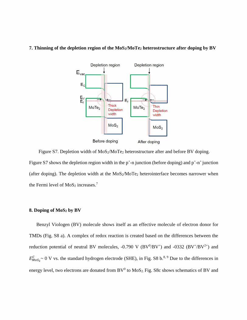
7. Thinning of the depletion region of the MoS2/MoTe2 heterostructure after doping by BV
Figure S7 shows the depletion region width in the p+-n junction (before doping) and p+-n+ junction
(after doping). The depletion width at the MoS2/MoTe2 heterointerface becomes narrower when
the Fermi level of MoS2 increases.7
8. Doping of MoS2 by BV
Benzyl Viologen (BV) molecule shows itself as an effective molecule of electron donor for
TMDs (Fig. S8 a). A complex of redox reaction is created based on the differences between the
reduction potential of neutral BV molecules, -0.790 V (BV0/BV+) and -0332 (BV+/BV2+) and
𝐸𝑀𝑜𝑆2
𝐶 ~ 0 V vs. the standard hydrogen electrode (SHE), in Fig. S8 b.8, 9 Due to the differences in
energy level, two electrons are donated from BV0 to MoS2. Fig. S8c shows schematics of BV and
Figure S7. Depletion width of MoS2/MoTe2 heterostructure after and before BV doping.

electrons transfer to MoS2 flakes. After the redox reaction, a complex between oxidized BV2+ and
a divalent acceptor2- is generated.
Figure S8. (a) Redox reaction of benzyl viologen molecules, (b) Energy band diagram of MoS2
conduction band and redox states of BV, (c) A schematic of MoS2, BV and electron transfer.
9. Calculation details
We performed quantum mechanical calculations within density functional theory (DFT)
framework. Atomic orbital basis sets were used as implemented in DMOL3 code10 in the double
numerical with polarization with additional diffuse functions (DNP+). All electrons, including
those from the core part, were considered during calculations. The exchange-correlation
functionals using generalized gradient approximation (GGA)11 and the k-points with Monkhorst-
Pack grid with a separation of 0.02/Å were used. Geometry optimization criteria were 0.005 Å for
distance, 0.001 Ha/Å for force, and 10-5 Ha for total energy difference.

The optimized bulk structures showed a = b = 3.1212 Å and c = 11.8410 Å for MoS2 and a =
b = 3.5644 Å and c = 13.5313 Å for MoTe2 respectively. The calculated energy band gap using
GGA-PBE functional were 1.067 eV for MoS2 and 0.777 eV for MoTe2. Comparing to the
experimental values a = b = 3.161 Å and c = 12.295 Å for MoS2 a = b = 3.519 Å and c = 13.964
Å for MoTe2, our method represents in reasonable agreement. The underestimation of band gap
by DFT calculation is well known. The difference of calculated band gaps between MoS2 and
MoTe2 was 0.29 eV, close to that of measured value of ca. 0.3 eV. Calculation data with
comparison to the experimental data for bulk systems are summarized in Table S1.
From the optimized bulk structure, we generated multi-layered structure and calculate the
electronic structures. We applied vacuum region as 15 Å in order to avoid any artificial inter-
supercell interaction.
Table S1. The calculated lattice constants and the electronic energy gap. All electron density
functional theory calculations using GGA-PBE functional were used.
MoS2/PBE MoS2/Expt. MoTe2/PBE MoTe2/Expt.
Lattice
const.(Å)
a c a c a c a c
3.1212 11.8410 3.161 12.295 3.5644 13.5313 3.519 13.964
Egap (eV) 1.067 1.23 12 0.777 0.88 13

Table S2. The calculated energy levels using all electron density functional theory scheme. The
reference was set to the Fermi level of the 13-layer MoTe2 supercell. VBM and CBM represent
the valence band maximum and the conduction band minimum, respectively. We used 15 Å of
vacuum in the calculation.
MoTe2 13-layerd MoS2 5-layered
EFermi (eV) 0 -0.309
Egap (eV) 0.779 1.137
VBM (eV) -0.182 -0.662
CBM (eV) 0.597 0.475
Height (Å) 87.9535 + vacuum 29.6025 + vacuum

Figure S9. The calculated supercells, i.e., 5-layered MoS2 (left) and 13-layered MoTe2 (right) in
ball and stick form.

Supplementary References:
1 B. Chakraborty, A. Bera, D. V. S. Muthu, S. Bhowmick, U. V. Waghmare and A. K. Sood,
Phys. Rev. B - Condens. Matter Mater. Phys., 2012, 85, 161403.
2 A. Castellanos-Gomez, R. Roldán, E. Cappelluti, M. Buscema, F. Guinea, H. S. J. Van Der
Zant and G. A. Steele, Nano Lett., 2013, 13, 5361–5366.
3 H. J. Conley, B. Wang, J. I. Ziegler, R. F. Haglund, S. T. Pantelides and K. I. Bolotin, Nano
Lett., 2013, 13, 3626–3630.
4 D. Kufer and G. Konstantatos, Nano Lett., 2015, 15, 7307–7313.
5 D. Subba Reddy, M. Siva Pratap Reddy and V. Rajagopal Reddy, Optoelectron. Adv. Mater.
Rapid Commun., 2011, 5, 448–454.
6 J. Miao, Z. Xu, Q. Li, A. Bowman, S. Zhang, W. Hu, Z. Zhou and C. Wang, ACS Nano,
2017, 11, 10472–10479.
7 D. K. Schroder, Semiconductor Material and Device Characterization: Third Edition, 2005.
8 S. Mouri, Y. Miyauchi and K. Matsuda, Nano Lett., 2013, 13, 5944–5948.
9 D. Kiriya, M. Tosun, P. Zhao, J. S. Kang and A. Javey, J. Am. Chem. Soc., 2014, 136, 7853–
7856.
10 B. Delley, J. Chem. Phys., 2000, 113, 7756–7764.
11 J. Perdew, K. Burke and M. Ernzerhof, Phys. Rev. Lett., 1996, 77, 3865–3868.
12 K. K. Kam and B. A. Parkinson, J. Phys. Chem., 1982, 86, 463–467.
13 I. G. Lezama, A. Ubaldini, M. Longobardi, E. Giannini, C. Renner, A. B. Kuzmenko and
A. F. Morpurgo, 2D Mater., 2014, 1, 21002–13.