parallel evaluation of the bii3, bioi, and ag3bii6 layered
TRANSCRIPT

General rights Copyright and moral rights for the publications made accessible in the public portal are retained by the authors and/or other copyright owners and it is a condition of accessing publications that users recognise and abide by the legal requirements associated with these rights.
Users may download and print one copy of any publication from the public portal for the purpose of private study or research.
You may not further distribute the material or use it for any profit-making activity or commercial gain
You may freely distribute the URL identifying the publication in the public portal If you believe that this document breaches copyright please contact us providing details, and we will remove access to the work immediately and investigate your claim.
Downloaded from orbit.dtu.dk on: Oct 31, 2021
Parallel evaluation of the BiI3, BiOI, and Ag3BiI6 layered photoabsorbers
Crovetto, Andrea; Hajijafarassar, Alireza; Hansen, Ole; Seger, Brian; Chorkendorff, Ib; Vesborg, PeterC.K.
Published in:Chemistry of Materials
Link to article, DOI:10.1021/acs.chemmater.9b04925
Publication date:2020
Document VersionPeer reviewed version
Link back to DTU Orbit
Citation (APA):Crovetto, A., Hajijafarassar, A., Hansen, O., Seger, B., Chorkendorff, I., & Vesborg, P. C. K. (2020). Parallelevaluation of the BiI
3, BiOI, and Ag
3BiI
6 layered photoabsorbers. Chemistry of Materials, 32(8), 3385-3395.
https://doi.org/10.1021/acs.chemmater.9b04925

Parallel evaluation of the BiI3, BiOI, and
Ag3BiI6 layered photoabsorbers
Andrea Crovetto,∗,†,¶ Alireza Hajijafarassar,‡ Ole Hansen,‡ Brian Seger,† Ib
Chorkendor�,† and Peter C. K. Vesborg∗,†
†Surfcat, DTU Physics, Technical University of Denmark, DK-2800 Kgs. Lyngby, Denmark
‡DTU Nanolab, Technical University of Denmark, DK-2800 Kgs. Lyngby, Denmark
¶Current address: Helmholtz-Zentrum Berlin für Materialien und Energie GmbH,
Glienicker Str. 100, 14109 Berlin, Germany.
E-mail: [email protected]; [email protected]
Abstract
The bismuth-based (oxy)iodides BiI3, BiOI and AgxBiIx+3 share similar layered
crystal structures, optimal band gaps for top absorbers in tandem solar cells, and
moderate synthesis temperatures. Similarly to halide perovskite absorbers, they contain
a heavy cation with a lone pair of electrons (Bi3+) which has been proposed as an
important feature enabling defect tolerance in perovskites. The aim of this work is
to grow and characterize BiI3, BiOI, and Ag3BiI6 absorbers and solar cells using a
consistent synthesis and analysis routine. In this way, the individual strengths and
weaknesses of the three absorbers, as well as their common challenges, can be outlined.
The proposed synthesis method based on (oxy)iodization of metallic precursor �lms
results in similar room-temperature photoluminescence features in all three materials,
possibly indicating a similar degree of defect tolerance. At the device level, the open
circuit voltage of BiI3 solar cells and the �ll factor of BiOI solar cells are improved
1

compared to their respective state of the art. To improve short circuit currents, control
of growth orientation should be a priority in view of the anisotropic properties of these
compounds. P-type bulk doping and selection of hole transport layers with deep valence
bands are also key areas for future work. Beyond photovoltaics, the very low (< 1.1)
dark diode ideality factor in BiI3 devices and the existence of both electronic and ionic
conduction in Ag3BiI6 may open up applications in other areas of optoelectronics.
Introduction
An important reason behind the remarkable performance of methylammonium lead iodide
(MAPbI3) and related Pb-based halide perovskites as solar absorbers is their combination
of high carrier lifetimes and relatively high mobilities, which together enable high minority
carrier lifetimes and di�usion lengths even in solution-processed �lms.1 These experimental
features indicate a high degree of defect tolerance, which can be rationalized based on funda-
mental features in their band structure.2�4 In particular, it has been suggested4 that defect
tolerance in halide perovskites may be linked to the presence of the heavy Pb2+ cation in a
partially oxidized state, i.e., with the ns2np0 electron con�guration retaining a lone pair of
electrons. On the one hand, interaction between the cation(s) lone-pair orbital and anion(p)
orbitals yields an antibonding valence band with high dispersion. These are prerequisites for
defect tolerance towards cation vacancies and high hole mobility respectively.2,3 On the other
hand, the large mass of Pb intensi�es spin-orbit coupling, which broadens the conduction
band (more dispersion) and pushes its minimum to a lower energy than the atomic Pb 6p
states. These are prerequisites for high electron mobility and defect tolerance towards anion
vacancies respectively.2,3 Besides their enhanced spin-orbit coupling, heavy cations have the
additional advantage that the relative stability of the partially oxidized state versus the fully
oxidized state typically increases down a column of the periodic table.
Since other materials containing a heavy, partially oxidized p-block element may exhibit
similar optoelectronic properties to halide perovskites, increasing attention has been devoted
2

Figure 1: Crystal structures of BiI3 (R3̄), BiOI (P4/nmm), and ABI (R3̄m). The latteris shown with the stoichiometry and occupations determined by Oldag et al.9 Note thecompletely disordered cation sublattice with fractional occupation by Ag and Bi, the smallAg population of normally vacant sites between the layers, and the absence of part of theAg expected from the Ag3BiI6 stoichiometry. The missing Ag is either delocalized in thelattice or present in the form of a AgI secondary phase.9,10 Also note the similarity betweenthe R3̄ structure of BiI3, where every third possible cation site is not occupied, and theR3̄m structure of ABI, where all possible cation sites are fractionally occupied. Green:Bi; orange: Ag; purple: I; red: O; white: vacancies. Sites with more than one color arefractionally occupied.
to ns2-containing solar absorbers, which are the subject of a recent review.5 Among the
heaviest cations (Tl+, Pb2+, and Bi3+), Bi3+ is especially interesting as Bi has no particular
toxicity concerns,6 is relatively inexpensive,7 and its compounds have not been widely inves-
tigated as solar absorbers. The speci�c �eld of Bi-containing compounds for photovoltaics
has been recently reviewed.7,8
Among a number of possible candidates, BiI3, BiOI, and a range of AgxBiIx+3 (ABI)
compounds have potential applications as top absorbers in tandem solar cells, since their
reported band gaps are in the 1.6-2.0 eV range.11,12,14,19,23�32 The highest single-junction cell
e�ciencies achieved until now are 1.2% for BiI3,14 1.8% for BiOI,19 and 4.3% for ABI with
x = 3 (Ag3BiI6).30 The valence bands maximum (VBM) has predominantly I 5p character
3

Absorber
m∗ e
m∗ h
CBM
VBM
ε rdopingtype
maindefects
material
(m0)
(m0)
(I-richregion)
BiI3‖c:
>1.811‖c:
>10
11
Bi6p
(∼60%)
I5p
(>90%)1
2‖c:
913
p12,14
VBi,I B
i(deep)1
5
⊥c:
0.75
16⊥
c:1.0-3.916
I5p
(∼40%)
Bi6s
(<10%)⊥
c:54
13
n17
VI(shallow)
BiOI‖c:
>118
‖c:
1.918
Bi6p
(∼60%)
I5p
(∼70%)1
846
11,19
n20,21
VBi(shallow)1
9
⊥c:∼0.318⊥
c:1.918
O2p∼I5p
O2p
>Bi6s
p22
VI(shallow)
ABI‖c:
1.8?
17‖c:
1.3?
17
Bi6p
(∼50%)
I5p
(>60%)1
7N.A.
p17
N.A
(R3̄m
)⊥
c:0.4?
17⊥
c:0.4?
17
I5p
(∼50%)
Bi6s?Ag4d?
n23
Table1:
Electronicproperties
ofBiI3,BiOI,andAg 3BiI6.Allproperties
arecalculatedexceptfordopingtype.m
0,m
∗ e,and
m∗ haretheelectron
massandthee�ective
massesofelectronsandholes
respectively.‖cand⊥
creferto
e�ective
massesalong
thecaxisandon
theabplanerespectively,as
show
nin
Fig.1.
TheVBM
andCBM
columnsreferto
theorbitalcharacterof
thevalence
bandmaximum
andconductionbandminimum
respectively.ε r
isthestatic(zero-frequency)relative
permittivity.
Thelisted
defectsarethosewiththelowestcalculatedform
ationenergy
underI-rich
grow
thconditions.Som
epropertiesofABI
arelabeled
withaquestion
mark,signalingahigher
uncertainty
dueto
themoreapproximatecomputational
approachused
tocalculate
thosequantities.Although
datafortherelative
permittivityanddefects
inABIarenot
available,thesituationis
likely
similar
tothecase
ofBiI3dueto
thesimilarityof
thetwocompounds.
4

in all three compounds, with a small contribution from Bi 6s states as expected from the
discussion above (Table 1). The overlap between Bi 6s and I 5p states is however not large
enough for the 6s2 lone pair to be stereochemically active,33 so Bi retains an undistorted
octahedral coordination in all compounds.11,18,30 For the case of BiOI, O 2p states also
contribute to the VBM (Table 1). In all cases, the conduction band maximum (CBM)
consists of a roughly equal mix of Bi 6p and I 5p states. Interestingly, these materials share
quite similar anisotropic crystal structures with layers held together by weak van der Waals
forces along the c axis (Fig. 1). It can be argued that layered structures are not optimal
for carrier transport as they tend to exhibit low band dispersion and high carrier e�ective
masses along the c axis due to poor orbital overlap. Indeed, �rst-principles calculations
predict relatively high e�ective masses along c for both carrier types in all three compounds
(Table 1). Despite this potential disadvantage, recent work on other layered compounds
(particularly Sb2Se3 and 2D perovskites)34,35 has shown that high photovoltaic e�ciencies
are still possible if �lm growth can be controlled so that the c axis is oriented in the plane
of the substrate and, thus, not in the main transport direction.
Among the three Bi-based compounds, ABI is the photoabsorber with the largest number
of papers reporting solar cell fabrication and with the highest reported e�ciency. However,
ABI is also the most poorly understood of the three, since it features a wide range of possible
compositions (0.5 < x < 3),10 two possible crystal structures (cubic Fd3̄m and rhomboedral
R3̄m),10,17,36 complete disorder in the Ag/Bi sublattice,9,30 partial occupation of (nominally
vacant) lattice sites between layers (Fig. 1),9 and a relatively low activation energy for Ag
migration (0.44 eV)9 implying potential ionic conduction. Possibly due to the structural
and compositional �exibility of the material, as well as to challenges related to modeling
disordered structures, detailed computational work on ABI using state-of-the-art methods
is lacking. Calculations on the cubic phase using hybrid functionals and spin-orbit coupling
dealt mainly with structural aspects.36 More detailed calculations were carried out recently
for both crystal structures of AgBiI4, but they relied on the less accurate generalized gradient
5

approximation, thus yielding drastically underestimated band gaps.17
In this work, we synthesize BiI3, BiOI, and ABI thin �lms under anion-rich condi-
tions using a two-step process, i.e., sputter deposition of metallic precursors followed by
(oxy)iodization at moderate temperatures. The motivation for employing a two-step process
is that anion-rich growth conditions can be realized in the second step by performing the
iodization process at atmospheric pressure. According to calculations, anion-rich conditions
should ensure a lower concentration of deep defects (VO in BiOI; BiI and Bi interstitials in
BiI3) which can be e�ective recombination centers.15,19 Since the e�ective masses in these
materials are generally lower for electrons than for holes (Table 1) the p-type conductivity
favored under anion-rich conditions15,19 is another possible advantage. To our knowledge,
a synthesis route based on (oxy)iodization of metallic precursors has not been explored for
BiI3, BiOI, or ABI. By employing a consistent synthesis and characterization routine for
BiI3, BiOI, and ABI, it is hoped that the present study can provide useful information for (i)
comparing the three absorbers on a fair basis and (ii) evaluating advantages and drawbacks
of the proposed two-step synthesis method for this class of materials.
Experimental details
Metallic Bi precursor �lms for BiI3 and BiOI were sputter-deposited from a Bi target. Metal-
lic precursor �lms for ABI were deposited by co-sputtering individual Bi and Ag targets at
suitable powers for obtaining an Ag-Bi alloy with Ag2Bi composition according to energy
dispersive x-ray spectroscopy (EDX). This particular precursor stoichiometry is appropri-
ate for obtaining a �nal ABI stoichiometry around Ag3BiI6, due to some BiI3 losses during
iodization. Following the device structures proposed in previous work,12,23 the precursor
�lms for BiI3 and ABI were deposited on a glass/FTO/TiO2 substrate, whereas the pre-
cursor �lms for BiOI were deposited on a glass/ITO/NiO substrate.19 Iodization of BiI3
and ABI was carried out at atmospheric pressure by subliming I2 lumps within a Petri dish
6
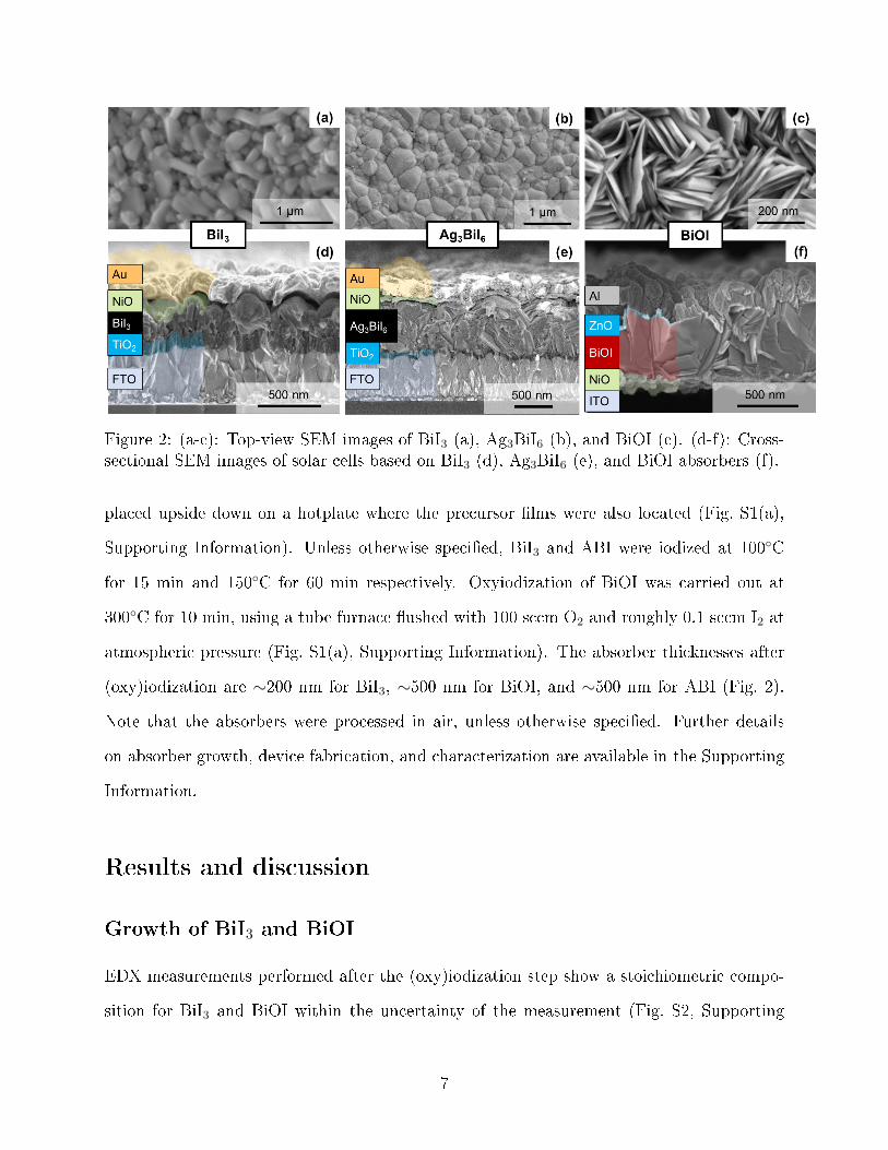
Figure 2: (a-c): Top-view SEM images of BiI3 (a), Ag3BiI6 (b), and BiOI (c). (d-f): Cross-sectional SEM images of solar cells based on BiI3 (d), Ag3BiI6 (e), and BiOI absorbers (f).
placed upside down on a hotplate where the precursor �lms were also located (Fig. S1(a),
Supporting Information). Unless otherwise speci�ed, BiI3 and ABI were iodized at 100◦C
for 15 min and 150◦C for 60 min respectively. Oxyiodization of BiOI was carried out at
300◦C for 10 min, using a tube furnace �ushed with 100 sccm O2 and roughly 0.1 sccm I2 at
atmospheric pressure (Fig. S1(a), Supporting Information). The absorber thicknesses after
(oxy)iodization are ∼200 nm for BiI3, ∼500 nm for BiOI, and ∼500 nm for ABI (Fig. 2).
Note that the absorbers were processed in air, unless otherwise speci�ed. Further details
on absorber growth, device fabrication, and characterization are available in the Supporting
Information.
Results and discussion
Growth of BiI3 and BiOI
EDX measurements performed after the (oxy)iodization step show a stoichiometric compo-
sition for BiI3 and BiOI within the uncertainty of the measurement (Fig. S2, Supporting
7

Information). X-ray di�raction (XRD) patterns are consistent with the rhombohedral R3̄
structure of BiI3 and the tetragonal P4/nmm structure of BiOI (Fig. 1), with additional
peaks corresponding to the FTO and ITO substrate respectively (Fig. 3(a,b)). Within the
detection limit of the XRD measurement, the �lms appear to be single-phase. The morphol-
ogy of BiI3 grown at 100◦C is shown in Fig. 2(a). Its morphology evolution with growth
temperature is shown in Fig. S3, Supporting information. BiI3 formation starts at around
70◦C, with the growth of small, isotropic grains. As the reaction temperature is increased,
some grains become more elongated until, at a temperature around 150◦C, a platelet mor-
phology with increasing c-axis texture begins to develop as observed by others.11,37,38 If the
reaction temperature is too low, the XRD peaks of BiI3 are weak and broad, and metallic
Bi remains as a secondary phase. If the reaction temperature is too high, BiI3 solar cells
exhibit very low photocurrents, presumably due to the presence of large, poorly connected
BiI3 platelets and the unfavorable transport properties along the c axis. A higher growth
temperature might, however, present other advantages, such as a higher photoluminescence
quantum yield,27 signaling a higher intrinsic material quality with a more favorable defect
landscape. A strong dependence of BiI3 material properties on growth temperature is re-
�ected in their corresponding device properties. As will be shown later, BiI3 �lms grown at
100◦C yield the most e�cient solar cells, but the �lms grown at 180◦C result in very low
diode ideality factors in the dark despite their poor photovoltaic performance.
BiOI growth proceeds �rst by conversion of Bi into BiI3, starting at around 100◦C. As
long as the I2 and O2 partial pressures are appropriate, conversion of BiI3 into BiOI begins
near the sublimation point of BiI3 (237◦C).15 If the I2 partial pressure is too high, BiI3
sublimes instead of forming BiOI. If the I2 partial pressure is too low, the reaction product
is Bi2O3 instead of BiOI. In practice, we found that BiOI processed at less than 280◦C still
contained spurious peaks in its XRD pattern. Since BiOI starts decomposing at 300◦C,39 the
accessible temperature window for converting BiI3 into BiOI is rather narrow (∼280-300◦C).
This is a disadvantage of the proposed two-step growth method, and is related to the fact
8

that any Bi lost due to decomposition cannot be recovered. Conversely, growth techniques
in which Bi, I, and O are supplied simultaneously (such as chemical vapor transport) can
maintain the substrate at higher temperatures as long as the deposition rate is higher than
the decomposition rate. In fact, the best BiOI cells by chemical vapor transport were made
at 350◦C.19 Similarly to previous reports using other deposition techniques19,40 BiOI �lms
made by oxyiodization of Bi precursors grow in the form of thin platelets that are often
oriented perpendicularly to the substrate plane (Fig. 2(c)). The BiOI platelets are generally
more densely packed then the BiI3 platelets obtained at high reaction temperatures, which
may be an advantage for carrier transport.
BiOI �lms grown by oxyiodization of metallic precursors su�er from poor adhesion of
BiOI on the hole transport layer, often resulting in BiOI peeling o� during the cooling
phase. Adhesion properties are clearly in�uenced by the nature of the underlying layer, as
BiOI �lms grown on bare quartz and on MoS2 had a much higher peel-o� rate than �lms
grown on NiO. It would be interesting to grow BiOI by direct conversion of metallic Bi
without the BiI3 intermediate, or by conversion of Bi2O3. The former option is, however,
hindered by the low melting point of Bi (271◦C) and by the ease of formation of BiI3 even
at very low I2 partial pressures. The latter option was attempted in this work but resulted
in only partial iodization of Bi2O3 and no single-phase BiOI could be obtained (more details
in the Supporting Information).
Growth of Ag3BiI6
Before describing the growth of ABI, it is worth discussing some of its compositional and
structural aspects. The occurrence of the rhomboedral R3̄m and cubic Fd3̄m crystal struc-
tures of ABI as a function of composition x has been the subject of some debate.9,10,17,30,36,41
The only possible stoichiometry in either structure that is compatible with both charge neu-
trality and with the absence of vacancies and interstitials is AgBiI4 (x = 1). However, it
was shown by two independent studies that, for x = 1, a mix of the two R3̄m and Fd3̄m
9

structures is obtained.10,41 For x > 1, the R3̄m structure is favored and it appears as a single
phase at compositions close to Ag2BiI5. For higher values of x, the R3̄m phase is present
together with a AgI secondary phase. The most e�cient ABI cells to date,30 as well as the
�lms produced in this work (x ∼ 3), fall into this category. For x < 1, the Fd3̄m structure is
favored and it appears as a single phase at compositions close to AgBi2I7. For lower values
of x, the Fd3̄m phase is present together with a BiI3 secondary phase. As mentioned above,
all stoichiometries for which x 6= 1 must contain a certain combination of vacancies and/or
interstitials to be compatible with any of the two crystal structures. For the R3̄m single
phase, Ag interstitials between the ab planes were identi�ed by Rietveld re�nement,9,10 and
those are shown in Fig. 1. For the Fd3̄m single phase, vacancies in the Ag/Bi sublattice
were identi�ed.10 Furthermore, a fraction of Ag was found to be completely delocalized in
the lattice.9 This is a hint that the performance of ABI solar cells may be in�uenced by
mobile ions, as in halide perovskite solar cells.
In the two-step process proposed in this work, Ag in Ag2Bi �lms reacts with I2 already
at room temperature to form AgI. From around ∼70◦C, Bi starts reacting both with I2 and
with AgI to form a mix of BiI3 and ABI. As the temperature is increased, the BiI3 impurity
content decreases. At a growth temperature of 150◦C, a hold time of 1 hour is necessary
to completely remove the BiI3 XRD peaks (Fig. S4, Supporting Information). The �lm
morphology consists of densely packed and rather isotropic crystal grains up to 500 nm in
diameter (Fig. 2(b)). Due to some loss of BiI3 during the hold step at 150◦C, the composition
of ABI �lms after iodization is usually close to the desired Ag3BiI6 stoichiometry according to
EDX (Fig. S2, Supporting Information).23 Employing iodization temperatures signi�cantly
higher than 150◦C is challenging because the increasing BiI3 loss would have to be �nely
counterbalanced either by more Bi-rich precursors or by a signi�cant BiI3 partial pressure
during iodization. The XRD pattern of the iodized �lm (Fig. 3(c)) indicates that ABI in the
R3̄m structure is present together with AgI secondary phases as expected from the x ∼ 3
ABI stoichiometry. Thus, the present ABI �lms have similar composition and structure
10

10 15 20 25 30 35 40 45 50 55 60 65 70 75 80 85 90 95 100
Log(
inte
nsity
) (ar
b. u
nits
)
Bi3(R-3)
BiI3 on TiO2/FTO***
*
SnO2
(b)
(003
)(1
01)
(105
)/(00
6)
(2-1
3)
(300
)
(303
)
(3-1
7)(4
-2 3
)
(5 -4
3)
(6 -3
0)
(2-1
6)
(2-1
9)
BiOI(P4/nmm)
BiOI on NiO/ITO*** *
In2O3
(001
)
(002
)
(101
)
(102
)
(110
)(1
11)
(103
)(1
12)
(004
)
(200
)/(10
4)
(201
)
(114
)
(105
)
(220
)/(21
4)
(213
)/(11
5)
(204
)
(205
)/(11
6)
(215
)(3
10)
(a)
(314
)
(322
)/(30
5)
2q (degrees)
Ag3BiI6 on TiO2/FTO** *
*
° *
*
*
**
*
* * **
* * **
*
* * *
**AgBiI4(R-3m)
SnO2g-AgI
°
°
(c)
(003
)
(101
)
(006
)(1
0-2)
°
(104
)(1
0-5)
(107
)/(00
9)(2
-10)
(10-
8)(2
-13)
(20-
1)(2
-16)
(00
12)
(2-1
9)(2
08)
(3-1
4)(2
-1 1
2)
(300
)(3
-1-8
)
23 24 25
Figure 3: Bragg-Brentano XRD patterns of a BiOI �lm on a NiO/ITO/glass substrate (a),a BiI3 �lm on a TiO2/FTO/glass substrate (b), and a Ag3BiI6 �lm on a TiO2/FTO/glasssubstrate (c). The patterns at the bottom of each sub�gure are reference patterns for ran-domly oriented �lms with collection codes 391354 (BiOI), 78791 (BiI3), 414635 (AgBiI4) and56552 (γ-AgI secondary phase) in the Inorganic Crystal Structure Database (ICSD). Thepeak positions expected for the ITO and FTO transparent contacts are also shown. The ex-perimental peaks assigned to the transparent contacts and to AgI are labeled with asterisksand circles respectively. Note that the strongest peak expected for TiO2 overlaps with the(006) peaks of BiI3 and Ag3BiI6. The (00X) peaks labeled in bold font arise from crystalliteswith the c axis oriented perpendicularly to the substrate plane, which are expected to below-mobility paths. The peaks labeled in blue or red are the dominant peaks in the higheste�ciency BiI3 and BiOI absorbers reported by others.14,19
to the ABI �lms from the highest e�ciency solar cells to date.30 It is perhaps surprising
that those cells were based on an impure absorber containing AgI secondary phases. AgI in
the α phase is one of the best-known ion conductors, but the α phase is only stable above
150◦C. As expected, the AgI peaks present in the room-temperature XRD pattern of ABI
(Fig. 3(c)) can be attributed to either the wurtzite β phase or the γ zincblende phase, but
not to the ion-conducting α phase. Nevertheless, a certain fraction of Ag in ABI appears
to be delocalized according to detailed XRD studies9 so it is conceivable that a Ag-rich
stoichiometry may promote not only the formation of AgI secondary phases, but also a
11

higher fraction of delocalized Ag in ABI. Therefore, mobile ions such as Ag+ in the x = 3
stoichiometry may have a bene�cial rather than a detrimental e�ect, possibly due to an
increased carrier selectivity of the absorber/transport layer interfaces where they are likely
to accumulate.42
The stability of BiI3, BiOI, and ABI was not studied systematically in this work. At a
purely visual level, BiOI appears to be the most stable of the three compounds with respect to
both air/moisture exposure and light. While BiOI does not change appearance after several
months of storage in ambient conditions, BiI3 turns yellow (Bi2O3)26 within some weeks of
storage in ambient air � a process that is accelerated by light exposure. Full Ag3BiI6 solar
cells undergo a noticeable color change within about a week, possibly due to Ag migration
or to other forms of interdi�usion across the layers. Ag3BiI6 is also unstable under electron
beam exposure in the SEM. Surface reactions and changes in the measured compositions are
clearly observed under high beam doses (Fig. S5, Supporting Information).
Texture
(001) and higher-order (00X) peaks are present in the XRD patterns of all three absorbers
(Fig. 3). Those peaks originate from crystallites having the c axis oriented perpendicularly
to the substrate plane (c-axis texturing). Since minority carriers must be transported in that
direction, c-axis texturing is likely associated with suboptimal carrier collection due to high
e�ective masses along the c axis (Table 1). By comparing the relative intensity of the (00X)
peaks with the intensity of other strong di�raction peaks in the experimental and reference
di�raction patterns (Fig. 3) it is straighforward to see that the trend in c-axis texturing is
Ag3BiI6 > BiOI > BiI3, with Ag3BiI6 (BiI3) being more (less) textured than a randomly
oriented �lm. Interestingly, the (00X) peaks in BiOI are broader than the peaks related to
any other orientation. As the peak width is inversely related to crystallite size, this fact
indicates that BiOI platelets are quite thin in the direction of the c axis, which can be easily
related to the morphology observed in SEM images (Fig. 2(c)).
12

Using the chemical vapor transport growth method,19 c-axis texturing of BiOI on NiO
was suppressed almost completely, possibly due to the higher achievable growth temperature
and to the highly tunable deposition rate. Due to the limited growth temperature window of
the two-step method (see previous section) it is unclear whether this method can achieve the
same level of texture control as chemical vapor transport. Orientation control in BiI3 and
ABI appears in general to be more challenging than in BiOI, as indicated by the signi�cant c-
axis texturing present in nearly all BiI3 and Ag3BiI6 cells reported in the literature, including
the ones with the highest e�ciency.14,28,29
Some di�erences in the most successful device architectures for each absorber can be
rationalized in terms of how challenging it is to obtain a c-axis-free texture in each mate-
rial. For ideally-oriented BiOI �lms on NiO, a conventional planar solar cell structure with
a relatively thick absorber (∼ 900 nm) was found to be appropriate. For the case of BiI3,
c-axis texturing is usually more pronounced at high growth temperatures, so a low absorber
thickness (∼ 200 nm) is typically chosen to obtain shorter collection paths and at the same
time allow the �lm to fully react at low process temperatures. Suppression of c-axis tex-
turing seems to be most challenging for ABI, hence the preference for a mesoporous device
architecture with very short collection paths in ABI solar cells. It must be emphasized that
a number of growth techniques which have enabled texture control in other layered materials
(vapor transport,43 closed-space sublimation,34 hot casting35) have not been widely explored
for BiI3 and ABI, so there may be opportunities for substantially improved texture control.
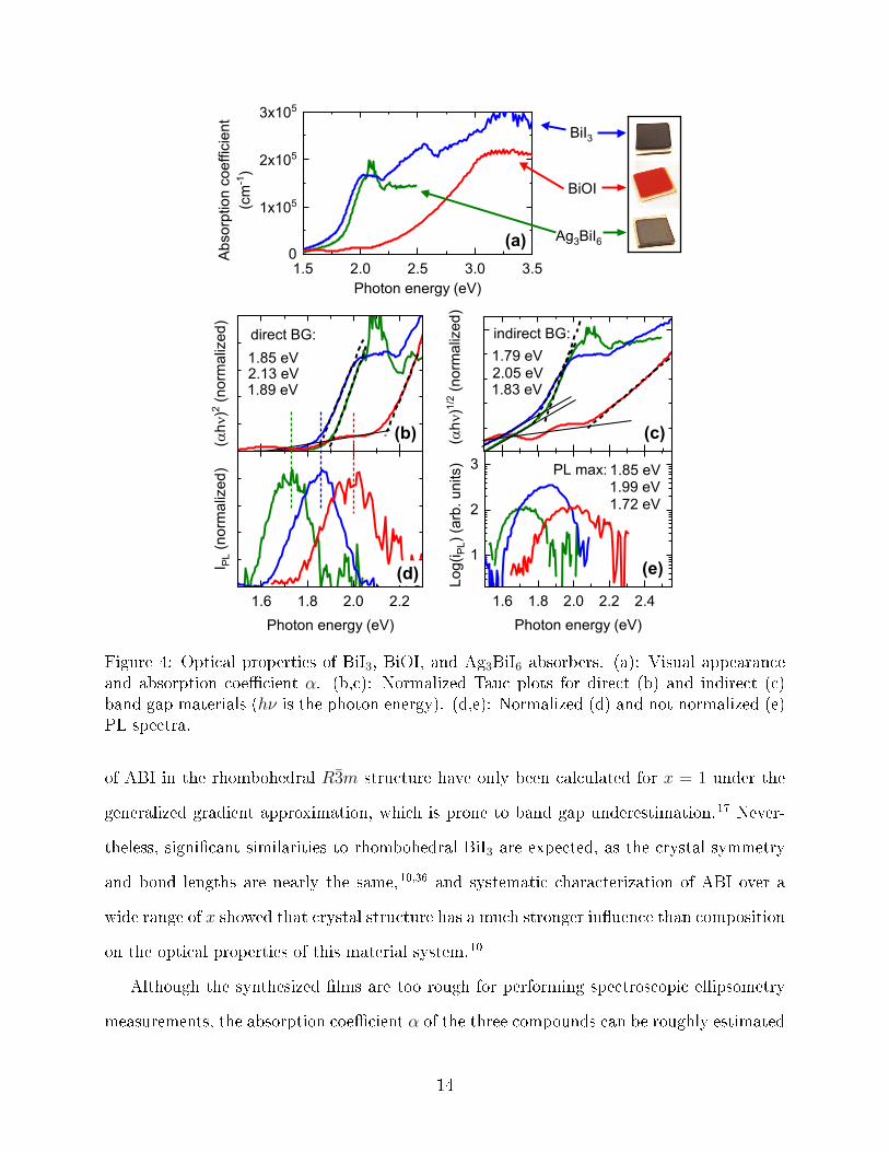
Band gaps
BiI3 and Ag3BiI6 �lms are dark grey in color, whereas BiOI is deep red (Fig. 4(a)). BiI3 and
BiOI are predicted to have indirect band gaps of 1.93 eV (BiI3)12 and 2.0 eV (BiOI)18 using
high-level computational methods with hybrid exchange correlation functionals and spin-
orbit coupling. However, the energy di�erence between the direct and indirect band gap is
small (0.1 eV or less) for both compounds.12,18 The band structure and optical properties
13
1.6 1.8 2.0 2.2 1.6 1.8 2.0 2.2 2.4
1
2
3
1.5 2.0 2.5 3.0 3.50
1x10⁵
2x10⁵
3x10⁵
(ahn
)2 (nor
mal
ized
)
direct BG:
(b)
1.85 eV
1.89 eV2.13 eV
I PL (
norm
aliz
ed)
Photon energy (eV)
(d) Log(
i PL)
(arb
. uni
ts)
Photon energy (eV)
1.85 eV1.99 eV1.72 eV
PL max:
(e)
(ahn
)1/2 (n
orm
aliz
ed)
2.05 eV1.83 eV
1.79 eVindirect BG:
(c)
Abs
orpt
ion
coef
ficie
nt(c
m-1
)
Photon energy (eV)
Ag3BiI6
BiOI
BiI3
(a)
Figure 4: Optical properties of BiI3, BiOI, and Ag3BiI6 absorbers. (a): Visual appearanceand absorption coe�cient α. (b,c): Normalized Tauc plots for direct (b) and indirect (c)band gap materials (hν is the photon energy). (d,e): Normalized (d) and not normalized (e)PL spectra.
of ABI in the rhombohedral R3̄m structure have only been calculated for x = 1 under the
generalized gradient approximation, which is prone to band gap underestimation.17 Never-
theless, signi�cant similarities to rhombohedral BiI3 are expected, as the crystal symmetry
and bond lengths are nearly the same,10,36 and systematic characterization of ABI over a
wide range of x showed that crystal structure has a much stronger in�uence than composition
on the optical properties of this material system.10
Although the synthesized �lms are too rough for performing spectroscopic ellipsometry
measurements, the absorption coe�cient α of the three compounds can be roughly estimated
14

from transmission spectra since their thickness is known.24 The absorption coe�cients of
BiI3 and Ag3BiI6 (Fig. 4(a)) rise steeply to over 105 cm−1 and have a small dip between
2.0 eV and 2.2 eV. In BiI3, those features are due to strongly bound excitons (180 meV
binding energy)44,45 that are mobile along the ab planes.45 As mentioned above, structural
similarity between Ag3BiI6 and BiI3 suggests that absorption features in Ag3BiI6 may be
due to similar excitonic e�ects. Conversely, absorption in BiOI is weaker (Fig. 4(a)), even at
higher photon energies than its presumed direct band gap energy. Weak absorption above
the direct band gap can be due to a number of electronic structure features, such as a low
joint density of states or dipole-forbidden transitions.46,47 Tauc plots for direct- and indirect
band gap materials (Fig. 4(b,c)) yield direct (indirect) band gap values of 1.85 eV (1.79 eV)
for BiI3, 2.13 eV (2.05 eV) for BiOI, and 1.89 eV (1.83 eV) for Ag3BiI6. Since the indirect
and direct band gaps are expected to be close in energy for all materials, it may be di�cult
to distinguish the weak indirect absorption from band tails just below the direct band gap,
especially in thin-�lm samples. Thus, the values of the direct band gaps will be quoted from
now on.
Photoluminescence
Room-temperature photoluminescence (PL) spectra of BiI3, BiOI, and Ag3BiI6 �lms are
shown in Fig. 4(d,e). The PL peak energy is 1.85 eV in BiI3, 1.99 eV in BiOI, and 1.72 eV
in Ag3BiI6. The peaks are rather broad for all materials. The full width at half maximum
(FWHM) is 0.23 eV for BiI3, 0.25 eV for BiOI, and 0.21 eV for Ag3BiI6. The BiI3 peak
is broadened more on the low-energy side, whereas the BiOI and Ag3BiI6 peaks are nearly
symmetric. The (detrimental) Stokes shift between band gap and PL peak is largest for
Ag3BiI6 (∼0.15 eV) and smallest for BiI3, where it is close to zero. The PL intensity, which
is related to quasi-Fermi level splitting in the absorber, does not vary dramatically from one
material to another. The BiI3 peak is ∼4 times more intense than the BiOI and Ag3BiI6
peaks, which have approximately equal intensities at equal excitation levels. Note that the
15

di�erences in PL intensity measured here cannot be rigorously converted into implied open
circuit voltage di�erences48 because an excitation intensity signi�cantly higher than 1 sun
was necessary to obtain PL spectra of su�cient quality (see characterization details in the
Supporting Information). The doping type of these materials is unclear, as contradicting
reports of n- and p-type doping exist for each compound (see Table 1). There is some
consensus, however, on the fact that their native doping levels are low and their resistivity
is high. In fact, the doping densities of the three absorbers grown in this work were too
low to be unambiguously determined by either Hall, thermovoltage, capacitance, or Kelvin
probe techniques. Thus, the high iodine chemical potential employed during growth was
likely not su�cient to obtain signi�cantly higher doping levels than in previous studies.
In weakly doped absorbers, high carrier lifetimes are particularly important to sustain a
su�ciently high excess carrier density and minimize series resistance.11 If very high lifetimes
cannot be obtained, p-type doping through extrinsic impurities could be a viable strategy.
Extrinsic doping would also ensure that electrons are the minority carriers in the device,
thus minimizing the detrimental e�ect of high hole e�ective masses.
Review of band positions
The absolute band positions of the three absorbers are reviewed graphically in Fig. 5. BiI3
and ABI are relatively well aligned to each other both in the valence band and in the con-
duction band. Therefore, it is reasonable to assume that most electron- and hole transport
layers (ETL and HTL respectively) should be interchangeable between BiI3 and ABI. How-
ever, the VBMs of BiI3 and ABI are clearly deeper than the VBM of the archetypical hybrid
perovskite absorber methylammonium lead iodide (MAPbI3). The inadequacy of HTLs bor-
rowed from perovskite technology has been recognized for BiI312 and, in fact, a large fraction
of the Voc de�cit with respect to the implied Voc derived from PL yield measurements may
be due to a large valence band cli� at the interface with the HTL.
While the CBMs of ABI and MAPbI3 are reasonably well aligned to each other (Fig. 5),
16
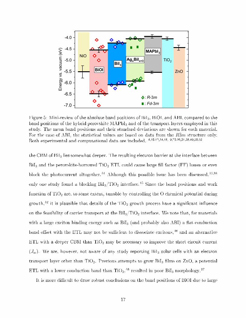
-7.0
-6.5
-6.0
-5.5
: R-3m: Fd-3m
-5.0
-4.5
-4.0
Ener
gy v
s. v
acuu
m (e
V)
BiOIBiI3
AgxBiIx+3
MAPbI3
TiO2
NiO
ZnO
Figure 5: Mini-review of the absolute band positions of BiI3, BiOI, and ABI, compared to theband positions of the hybrid perovskite MAPbI3 and of the transport layers employed in thisstudy. The mean band positions and their standard deviations are shown for each material.For the case of ABI, the statistical values are based on data from the R3̄m structure only.Both experimental and computational data are included. 4,10,12,14,18,19,23,26,31,38,49,50,53
the CBM of BiI3 lies somewhat deeper. The resulting electron barrier at the interface between
BiI3 and the perovskite-borrowed TiO2 ETL could cause large �ll factor (FF) losses or even
block the photocurrent altogether.51 Although this possible issue has been discussed,15,38
only one study found a blocking BiI3/TiO2 interface.45 Since the band positions and work
function of TiO2 are, to some extent, tunable by controlling the O chemical potential during
growth,52 it is plausible that details of the TiO2 growth process have a signi�cant in�uence
on the feasibility of carrier transport at the BiI3/TiO2 interface. We note that, for materials
with a large exciton binding energy such as BiI3 (and probably also ABI) a �at conduction
band o�set with the ETL may not be su�cient to dissociate excitons,48 and an alternative
ETL with a deeper CBM than TiO2 may be necessary to improve the short circuit current
(Jsc). We are, however, not aware of any study reporting BiI3 solar cells with an electron
transport layer other than TiO2. Previous attempts to grow BiI3 �lms on ZnO, a potential
ETL with a lower conduction band than TiO2,53 resulted in poor BiI3 morphology.
27
It is more di�cult to draw robust conclusions on the band positions of BiOI due to large
17

scattering in the reported values (Fig. 5). The overall trend, however, is a deeper location of
both the VBM and the CBM. Compatibly with this trend, the ETL in the best BiOI cell to
date19 is ZnO. BiOI cells with a TiO2 electron transport layer exhibited a roll-over e�ect19
which is a typical symptom of a barrier to carrier transport.54 Considering the average VBM
position reported for BiOI (Fig. 5), identi�cation of a new HTL with a deep VBM seems to
be even more urgent for BiOI solar cells than for BiI3 and ABI cells.
Photovoltaic properties
Single-junction BiI3 and Ag3BiI6 solar cells are completed by sputtering a NiO HTL and a
Au hole contact (Fig. 2(a,b)). Single-junction BiOI solar cells are completed by depositing
a ZnO ETL by atomic layer deposition and an Al electron contact by sputtering (Fig. 2(c)).
All three types of solar cells are illuminated through the glass substrate. However, BiOI
cells have the hole contact on the illuminated side, whereas BiI3 and Ag3BiI6 cells have the
electron contact on the illuminated side. Since the goal of this study is to evaluate the
two-step absorber growth method rather than experiment with alternative contact materials
and layer thicknesses, device structures are intentionally similar to the structures of the
highest-e�ciency cells reported for each absorber material.
The highest power conversion e�ciency in this work (η = 0.66%) is achieved by BiOI
solar cells, primarily due to a much higher Jsc and, secondarily, to a higher FF compared to
BiI3 and Ag3BiI6 solar cells (Fig. 6(a)). Considering that BiOI has a higher band gap and
weaker absorption than the other two absorbers (Fig. 4), the lower Jsc recorded in BiI3 and
Ag3BiI6 cells should be attributed to poor carrier collection rather than to a lower absorbed
photon �ux. The Jsc trend across the three absorbers (BiOI > BiI3 > Ag3BiI6) can be
related to various factors limiting carrier collection, such as di�erences in c-axis texturing
and morphology of the �lms, as well as di�erences in band alignment with the ETL. Ag3BiI6
is the absorber with the highest degree of c-axis texturing (Fig. 3), which is expected to
be detrimental for both Jsc and FF due to collection losses associated with crossing the
18
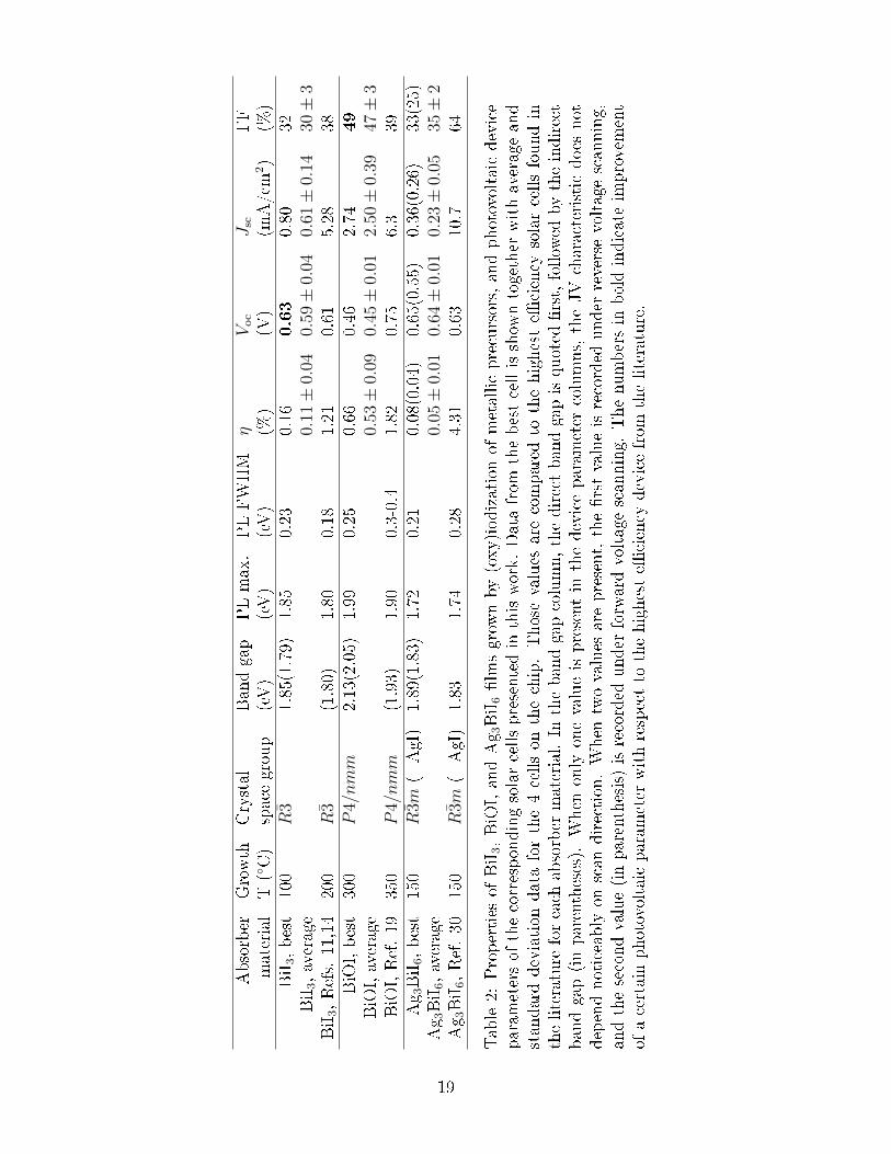
Absorber
Growth
Crystal
Bandgap
PLmax.
PLFWHM
ηVoc
Jsc
FF
material
T(◦C)
spacegroup
(eV)
(eV)
(eV)
(%)
(V)
(mA/cm
2)
(%)
BiI3,best
100
R3̄
1.85(1.79)
1.85
0.23
0.16
0.63
0.80
32BiI3,average
0.11±
0.04
0.59±
0.04
0.61±
0.14
30±
3BiI3,Refs.11,14
200
R3̄
(1.80)
1.80
0.18
1.21
0.61
5.28
38BiOI,best
300
P4/nmm
2.13(2.05)
1.99
0.25
0.66
0.46
2.74
49
BiOI,average
0.53±
0.09
0.45±
0.01
2.50±
0.39
47±
3BiOI,Ref.19
350
P4/nmm
(1.93)
1.90
0.3-0.4
1.82
0.75
6.3
39Ag 3BiI6,best
150
R3̄m
(+AgI)
1.89(1.83)
1.72
0.21
0.08(0.04)
0.65(0.55)
0.36(0.26)
33(25)
Ag 3BiI6,average
0.05±
0.01
0.64±
0.01
0.23±
0.05
35±
2Ag 3BiI6,Ref.30
150
R3̄m
(+AgI)
1.83
1.74
0.28
4.31
0.63
10.7
64
Table2:
Properties
ofBiI3,BiOI,andAg 3BiI6�lmsgrow
nby(oxy)iodizationof
metallicprecursors,andphotovoltaicdevice
param
etersof
thecorrespondingsolarcellspresentedin
thiswork.Datafrom
thebestcellisshow
ntogether
withaverageand
standarddeviation
dataforthe4cellson
thechip.Thosevalues
arecompared
tothehigheste�
ciency
solarcellsfoundin
theliterature
foreach
absorber
material.In
thebandgapcolumn,thedirectbandgapisquoted
�rst,follow
edbytheindirect
bandgap(inparentheses).
When
only
onevalueispresentin
thedeviceparam
eter
columns,theJV
characteristicdoes
not
dependnoticeably
onscan
direction.When
twovalues
arepresent,the�rstvalueisrecorded
under
reversevoltagescanning,
andthesecondvalue(inparenthesis)isrecorded
under
forwardvoltagescanning.
Thenumbersin
boldindicateimprovement
ofacertainphotovoltaicparam
eter
withrespectto
thehigheste�
ciency
devicefrom
theliterature.
19

-0.4 -0.2 0.0 0.2 0.4 0.6 0.8 1.0-2
-1
0
1
2
3
4
forward
0.0 0.2 0.4 0.6
0.0
0.2
0.4
0.6
0.8
-0.5 0.0 0.5 1.0-10
-8
-6
-4
-2
0
Cur
rent
den
sity
(mA/
cm2 )
Voltage (V)
BiOI
BiI3
darkcurves
(c)
Ag3BiI6
Cur
rent
den
sity
(mA/
cm2 )
Voltage (V)
(a)
(b)
reverse
Ag3BiI6
BiI3
Cur
rent
den
sity
(mA/
cm2 )
Voltage (V)
n = 1.006 ± 0.014
Figure 6: (a,b): JV characteristics of the single-junction BiI3, BiOI, and Ag3BiI6 solarcells produced in this work, recorded in the dark and under 1 sun illumination. (b) is azoomed-in view of (a), showing signi�cant hysteresis in the illuminated JV characteristic ofthe Ag3BiI6 solar cell. For all cells, the reverse JV scan is plotted as a solid line and theforward JV scan is plotted as a dotted line. The hysteresis characteristics of each type ofcell are representative of all cells fabricated with the processes described in this paper. (c):Dark and illuminated JV characteristics (solid and dashed line respectively) of a separateBiI3 solar cell, where BiI3 was grown at 180◦C instead of at 100◦C. The value of the darkdiode ideality factor n is obtained by a least-squares �t of the dark JV characteristic withthe single-diode equation (Fig. S6, Supporting Information). The value is con�rmed by analternative analysis method (Fig. S7, Supporting Information) and is a general characteristicof BiI3 diodes grown at 180◦C (Fig. S8, Supporting Information).
layer planes. Although BiOI has more pronounced c-axis texturing than BiI3 (Fig. 3), most
BiOI platelets extend from top to bottom of the �lm, whereas the BiI3 crystallites are
smaller (compare Fig. 2(d) and Fig. 2(f)). Furthermore, an electron barrier may exist at the
BiI3/TiO2 interface depending on the TiO2 preparation conditions, as explained earlier in
the paper.
20
Interestingly, the Voc trend in this study is the reverse of the Jsc trend discussed above.
BiOI cells display the lowest Voc, whereas BiI3 cells have a slightly better Voc than the best
BiI3 devices in the literature (Table 2). As noted in the discussion of PL spectra, these Voc
di�erences are unlikely to arise from large di�erences in the bulk material quality between the
three absorbers because their PL yields are within the same order of magnitude (Fig. 4(e)).
Di�erences in the absorber/HTL band alignment are, on the other hand, likely to contribute
to the Voc trend. As the HTL material is the same (NiO) for all three absorbers, the absorber
with the deepest valence band (BiOI) is the one where the largest Voc losses are expected
at the absorber/HTL interface.51 Photovoltaic parameters of the solar cells fabricated here
with the two-step method are compared in Table 2 to the photovoltaic parameters of the
highest e�ciency cells reported for each absorber. The overarching trend is that Voc values
are generally comparable, but Jsc values are much lower with the two-step method, resulting
in lower e�ciencies. The positive Voc results could be attributed to the anion-rich growth
conditions and the relatively high purity of vacuum-processed metallic precursors. The neg-
ative Jsc results could be attributed to non-optimal texture control, absence of a mesoporous
ETL (for ABI), and a possible barrier at the BiI3/TiO2 interface. As often reported in the
literature23,32,49,55 the present ABI cells exhibit scan rate-dependent hysteresis (Fig. 6(b)).
Considering the low activation energy for Ag ionic conduction in ABI,9 Ag+ migration within
the absorber during voltage scanning is the most likely cause of the hysteresis e�ect. Hystere-
sis is also observed in tandem ABI/silicon cells fabricated using a recently proposed device
structure (Fig. S9, Supplementary Information).56 The performance of the tandem cells is
not discussed further, as their negligible e�ciency points to additional device-related issues
that go beyond the ABI absorber quality.
Finally we note that, even though BiI3 grown at temperatures above 100◦C results in a
lower photovoltaic e�ciency, the dark ideality factors of BiI3 cells grown at 180◦C are consis-
tently close to 1, as shown in Fig. 6(c) and con�rmed in Figs. S6-S8, Supporting Information.
While the physical origin of this surprising behavior is still under investigation, high-quality
21

diodes combined with a low synthesis temperature could open up future applications of BiI3
within �exible electronics.
Conclusion and outlook
We synthesized thin �lms of BiI3, BiOI, and Ag3BiI6 by a two step method involving
(oxy)iodization of metallic precursors. We performed basic characterization of the three
materials and tested their performance as solar absorbers by producing single-junction pho-
tovoltaic devices. By growing and characterizing the three materials with the same methods,
they could be compared as objectively as possible, with the caveat that the absorber thick-
nesses and device structures were not kept �xed but were inspired by previous literature
results instead. This choice was made due to the di�erences in the absorption coe�cient and
band positions of the three absorbers.
The three bismuth-based (oxy)halides have some common features, such as low to mod-
erate synthesis temperatures, layered crystal structures with large e�ective masses perpen-
dicularly to the crystal layers, optimal band gaps for top absorbers in tandem solar cells,
and relatively deep valence bands. Although Bi appears as a compelling replacement for Pb
in perovskite-inspired materials, the "defect tolerance" of these Bi (oxy)iodides is question-
able (at least for acceptor defects) because the energy alignment of I 5p states with Bi 6s
states is poorer than their alignment with Pb 6s states.58 Poor energy alignment between
these orbitals limits their interaction and prevents the formation of a disperse, strongly an-
tibonding valence band maximum. In fact, Table 1 shows that Bi 6s states only contribute
minimally to the valence band maximum, hole e�ective masses are large in all directions,
and deep acceptor defects are expected, at least for BiI3. As the conduction bands of these
materials are, in general, more disperse and with stronger orbital mixing (Table 1) p-type
background doping may be preferable in order to have the more mobile electrons as mi-
nority carriers. The room-temperature photoluminescence spectra of these compounds are
22

Material:
BiI
3Material:
BiO
IMaterial:
AgxBiI
x+3
Method:
(oxy)iodization
ofmetallic
precu
rsors
Advantages
Strong
absorption,
low
grow
thtemperature.
Stable,goodtexturecon-
trol,
moderate
grow
thtemperature.
Strong
absorption,
low
grow
thtemperature.
High
Voc
(BiI3),
anion-
rich
grow
th,
high-quality
vacuum-processed
metals.
Disadvantages
Softandpotentially
un-
stable,poor
texture
con-
trol,deepVBM,highex-
citonbindingenergy.
Weak
absorption,
very
deep
VBM,poor
adhe-
sion
tosubstrate.
Softandpotentially
un-
stable,poor
texture
con-
trol,deepVBM,hystere-
sis.
Generally
low
Jsc,
in-
complete
texture
control,
limited
grow
thT
window
(BiOI).
Potential
areas
forinvestigation
Improvedtexture
control
athigher
grow
thT,ex-
perimentaldefectcharac-
terization,new
HTL,p-
typedoping.
Illuminating
from
elec-
tron
contact
side,experi-
mentaldefectcharacteri-
zation,new
HTL,p-type
doping.
Extra
electronic
struc-
ture
calculations,
exper-
imentaldefectcharacter-
ization,roleofionmigra-
tion,new
HTL,p-type
doping.
Using
seed
layers
topro-
motetexturing,
includinga
p-typedopantintheprecur-
sors,grow
ingBiOIdirectly
from
BiwithouttheBiI3in-
term
ediate
Table3:
Summaryof
advantagesanddisadvantagesof
Bi 3,BiOI,andAg 3BiI6absorbersin
general,as
wellas
ofthetwo-step
processusedto
grow
them
inthiswork.Suggestionsforfuture
workarealso
given.
23

generally rather weak and broad, so potential limitations due to native defects should be
further investigated experimentally. Partially compensating other unfavorable features, BiI3
and BiOI have very large static relative permittivities (although probably only along the
ab planes), which may help screen charged defects and decrease their capture cross section.
Unfortunately, the relative permittivity, the defect landscape, and even accurate e�ective
masses and band edge orbital character are not available for the family of ABI absorbers.17
More detailed calculations are thus called for.
While the three absorbers considered in this study certainly have some common features,
they also have substantial di�erences in their absorption coe�cient, ease of texture control,
growth temperature, and stability. Advantages and disadvantages of the individual absorbers
are summarized in Table 3. The results of this work and a review of the existing literature
suggest that the photovoltaic performance of all three materials would strongly bene�t if
their texture could be controlled so to obtain ab planes oriented perpendicularly to the
substrate plane. Texture control was a key step in unlocking the photovoltaic potential of
other layered compounds (Sb2Se3 and 2D perovskites) enabling e�ciencies above 10%.35 In
the present work, texture control was only achieved partially for BiOI and BiI3, and not
at all for Ag3BiI6. In previous studies using di�erent deposition techniques, the growth of
textured �lms was rarely mentioned as a priority and not achieved in practice, with possibly
only one exception.19 Therefore, the best BiI3 and Ag3BiI6 solar cells still need either a
very thin absorber or a mesoporous architecture to mitigate the poor collection e�ciency
related to carrier transport perpendicularly to the crystal layers.14,30 Future work on these
compounds should focus on growth techniques that are likely to enable texture control,
such as vapor transport and closed-space sublimation. There is also no guarantee that the
absorber thicknesses and device structures employed so far in the literature are optimal.
BiI3, BiOI, and ABI solar cells produced by (oxy)iodization of metallic precursors had
similar open circuit voltages (Voc) to the best devices reported for each absorber (except
for BiOI), but signi�cantly lower short circuit currents. The particularly low Jsc of Ag3BiI6
24
cells was attributed to a combination of poor texture control combined with the absence of
a mesoporous TiO2 layer aiding carrier collection. Beyond the original goal of evaluating
the photovoltaic performance of these materials, the low ideality factors of BiI3 diodes in
the dark (< 1.1), combined with a low synthesis temperature (< 200◦C) could make BiI3 an
attractive material for �exible electronics. Furthermore, the combined electronic and ionic
conductivity of ABI could be used to create light-controlled memristors and synaptic devices
as already demonstrated for halide perovksites.57,59
Supporting Information
Further experimental details, photographs of growth setups, EDX spectra, additional XRD
patterns and SEM images, determination of the ideality factor of BiI3 diodes, device structure
and JV characteristics of an ABI/silicon tandem cell.
Acknowledgements
This work was supported by VILLUM Fonden (grant no. 9455) and the Innovation Fund
Denmark (grant no. 6154-00008A). This project has received funding from the European
Union's Horizon 2020 research and innovation programme under the Marie Skªodowska-Curie
grant agreement No 840751.
References
(1) Stranks, S. D.; Eperon, G. E.; Grancini, G.; Menelaou, C.; Alcocer, M. J. P.; Lei-
jtens, T.; Herz, L. M.; Petrozza, A.; Snaith, H. J. Electron-Hole Di�usion Lengths
Exceeding 1 Micrometer in an Organometal Trihalide Perovskite Absorber. Science
2013, 342, 341�344.
25

(2) Zhang, S. B.; Wei, S.-H.; Zunger, A.; Katayama-Yoshida, H. Defect physics of the
CuInSe2 chalcopyrite semiconductor. Physical Review B 1998, 57, 9642�9656.
(3) Zakutayev, A.; Caskey, C. M.; Fioretti, A. N.; Ginley, D. S.; Vidal, J.; Stevanovi¢, V.;
Tea, E.; Lany, S. Defect Tolerant Semiconductors for Solar Energy Conversion. The
Journal of Physical Chemistry Letters 2014, 5, 1117�1125.
(4) Brandt, R. E.; Stevanovi¢, V.; Ginley, D. S.; Buonassisi, T. Identifying defect-tolerant
semiconductors with high minority-carrier lifetimes: beyond hybrid lead halide per-
ovskites. MRS Communications 2015, 5, 265�275.
(5) Ganose, A. M.; Savory, C. N.; Scanlon, D. O. Beyond methylammonium lead iodide:
prospects for the emergent �eld of ns2 containing solar absorbers. Chemical Communi-
cations 2017, 53, 20�44.
(6) Mohan, R. Green bismuth. Nature Chemistry 2010, 2, 336�336.
(7) Miller, N. C.; Bernechea, M. Research Update: Bismuth based materials for photo-
voltaics. APL Materials 2018, 6, 084503.
(8) Lee, L. C.; Huq, T. N.; MacManus-Driscoll, J. L.; Hoye, R. L. Z. Research Update:
Bismuth-based perovskite-inspired photovoltaic materials. APL Materials 2018, 6,
084502.
(9) Oldag, T.; Aussieker, T.; Keller, H.-L.; Preitschaft, C.; P�tzner, A. Solvothermale
Synthese und Bestimmung der Kristallstrukturen von AgBiI4 und Ag3BiI6. Zeitschrift
für anorganische und allgemeine Chemie 2005, 631, 677�682.
(10) Koedtruad, A.; Goto, M.; Amano Patino, M.; Tan, Z.; Guo, H.; Nakamura, T.;
Handa, T.; Chen, W.-T.; Chuang, Y.-C.; Sheu, H.-S.; Saito, T.; Kan, D.; Kanemitsu, Y.;
Wakamiya, A.; Shimakawa, Y. Structure�property relations in Ag�Bi�I compounds:
26

potential Pb-free absorbers in solar cells. Journal of Materials Chemistry A 2019, 7,
5583�5588.
(11) Brandt, R. E.; Kurchin, R. C.; Hoye, R. L. Z.; Poindexter, J. R.; Wilson, M. W. B.;
Sulekar, S.; Lenahan, F.; Yen, P. X. T.; Stevanovi¢, V.; Nino, J. C.; Bawendi, M. G.;
Buonassisi, T. Investigation of Bismuth Triiodide (BiI3) for Photovoltaic Applications.
The Journal of Physical Chemistry Letters 2015, 6, 4297�4302.
(12) Lehner, A. J.; Wang, H.; Fabini, D. H.; Liman, C. D.; Hébert, C.-A.; Perry, E. E.;
Wang, M.; Bazan, G. C.; Chabinyc, M. L.; Seshadri, R. Electronic structure and pho-
tovoltaic application of BiI3. Applied Physics Letters 2015, 107, 131109.
(13) Du, M.-H.; Singh, D. J. Enhanced Born charges in III-VII, IV-VII2, and V-VII3 com-
pounds. Physical Review B 2010, 82, 045203.
(14) Tiwari, D.; Alibhai, D.; Fermin, D. J. Above 600 mV Open-Circuit Voltage BiI3 Solar
Cells. ACS Energy Letters 2018, 3, 1882�1886.
(15) Cho, S. B.; Gazquez, J.; Huang, X.; Myung, Y.; Banerjee, P.; Mishra, R. Intrinsic point
defects and intergrowths in layered bismuth triiodide. Physical Review Materials 2018,
2, 064602.
(16) Zhang, W.-B.; Xiang, L.-J.; Li, H.-B. Theoretical perspective of energy harvesting
properties of atomically thin BiI3. Journal of Materials Chemistry A 2016, 4, 19086�
19094.
(17) Sansom, H. C.; Whitehead, G. F. S.; Dyer, M. S.; Zanella, M.; Manning, T. D.;
Pitcher, M. J.; Whittles, T. J.; Dhanak, V. R.; Alaria, J.; Claridge, J. B.; Rossein-
sky, M. J. AgBiI4 as a Lead-Free Solar Absorber with Potential Application in Photo-
voltaics. Chemistry of Materials 2017, 29, 1538�1549.
27

(18) Ganose, A. M.; Cu�, M.; Butler, K. T.; Walsh, A.; Scanlon, D. O. Interplay of Or-
bital and Relativistic E�ects in Bismuth Oxyhalides: BiOF, BiOCl, BiOBr, and BiOI.
Chemistry of Materials 2016, 28, 1980�1984.
(19) Hoye, R. L. Z. et al. Strongly Enhanced Photovoltaic Performance and Defect Physics
of Air-Stable Bismuth Oxyiodide (BiOI). Advanced Materials 2017, 29, 1702176.
(20) Hahn, N. T.; Hoang, S.; Self, J. L.; Mullins, C. B. Spray Pyrolysis Deposition and
Photoelectrochemical Properties of n-Type BiOI Nanoplatelet Thin Films. ACS Nano
2012, 6, 7712�7722.
(21) Bhachu, D. S.; Moniz, S. J. A.; Sathasivam, S.; Scanlon, D. O.; Walsh, A.;
Bawaked, S. M.; Mokhtar, M.; Obaid, A. Y.; Parkin, I. P.; Tang, J.; Carmalt, C. J.
Bismuth oxyhalides: synthesis, structure and photoelectrochemical activity. Chemical
Science 2016, 7, 4832�4841.
(22) Cheng, H.; Huang, B.; Dai, Y. Engineering BiOX (X = Cl, Br, I) nanostructures for
highly e�cient photocatalytic applications. Nanoscale 2014, 6, 2009.
(23) Khazaee, M.; Sardashti, K.; Chung, C.-C.; Sun, J.-P.; Zhou, H.; Bergmann, E.; Dunlap-
Shohl, W. A.; Han, Q.; Hill, I. G.; Jones, J. L.; Lupascu, D. C.; Mitzi, D. B. Dual-
source evaporation of silver bismuth iodide �lms for planar junction solar cells. Journal
of Materials Chemistry A 2019, 7, 2095�2105.
(24) Podraza, N. J.; Qiu, W.; Hinojosa, B. B.; Motyka, M. A.; Phillpot, S. R.; Baciak, J. E.;
Trolier-McKinstry, S.; Nino, J. C. Band gap and structure of single crystal BiI3 : Re-
solving discrepancies in literature. Journal of Applied Physics 2013, 114, 033110.
(25) Coutinho, N. F.; Merlo, R. B.; Borrero, N. F. V.; Marques, F. C. Thermal Evaporated
Bismuth Triiodide (BiI3) Thin Films for Photovoltaic Applications. MRS Advances
2018, 1�4.
28

(26) Hamdeh, U. H.; Nelson, R. D.; Ryan, B. J.; Bhattacharjee, U.; Petrich, J. W.; Pan-
thani, M. G. Solution-processed BiI3 thin �lms for photovoltaic applications: Improved
carrier collection via solvent annealing. Chemistry of Materials 2016, 28, 6567�6574.
(27) Williamson, B. W.; Eickemeyer, F. T.; Hillhouse, H. W. Solution-Processed BiI3 Films
with 1.1 eV Quasi-Fermi Level Splitting: The Role of Water, Temperature, and Solvent
during Processing. ACS Omega 2018, 3, 12713�12721.
(28) Ghosh, B.; Wu, B.; Guo, X.; Harikesh, P. C.; John, R. A.; Baikie, T.; Arramel,; Wee, A.
T. S.; Guet, C.; Sum, T. C.; Mhaisalkar, S.; Mathews, N. Superior Performance of Sil-
ver Bismuth Iodide Photovoltaics Fabricated via Dynamic Hot-Casting Method under
Ambient Conditions. Advanced Energy Materials 2018, 8, 1802051.
(29) Zhu, H.; Pan, M.; Johansson, M. B.; Johansson, E. M. J. High Photon-to-Current Con-
version in Solar Cells Based on Light-Absorbing Silver Bismuth Iodide. ChemSusChem
2017, 10, 2592�2596.
(30) Turkevych, I.; Kazaoui, S.; Ito, E.; Urano, T.; Yamada, K.; Tomiyasu, H.; Yamag-
ishi, H.; Kondo, M.; Aramaki, S. Photovoltaic Rudor�tes: Lead-Free Silver Bismuth
Halides Alternative to Hybrid Lead Halide Perovskites. ChemSusChem 2017, 10, 3754�
3759.
(31) Kim, Y.; Yang, Z.; Jain, A.; Voznyy, O.; Kim, G.-H.; Liu, M.; Quan, L. N.; García
de Arquer, F. P.; Comin, R.; Fan, J. Z.; Sargent, E. H. Pure Cubic-Phase Hybrid
Iodobismuthates AgBi2I7 for Thin-Film Photovoltaics. Angewandte Chemie Interna-
tional Edition 2016, 55, 9586�9590.
(32) Zhang, Q.; Wu, C.; Qi, X.; Lv, F.; Zhang, Z.; Liu, Y.; Wang, S.; Qu, B.; Chen, Z.;
Xiao, L. Photovoltage Approaching 0.9 V for Planar Heterojunction Silver Bismuth
Iodide Solar Cells with Li-TFSI Additive. ACS Applied Energy Materials 2019, 2,
3651�3656.
29

(33) Walsh, A.; Payne, D. J.; Egdell, R. G.; Watson, G. W. Stereochemistry of post-
transition metal oxides: revision of the classical lone pair model. Chemical Society
Reviews 2011, 40, 4455.
(34) Zhou, Y.; Wang, L.; Chen, S.; Qin, S.; Liu, X.; Chen, J.; Xue, D.-J.; Luo, M.; Cao, Y.;
Cheng, Y.; Sargent, E. H.; Tang, J. Thin-�lm Sb2Se3 photovoltaics with oriented one-
dimensional ribbons and benign grain boundaries. Nature Photonics 2015, 9, 409�415.
(35) Tsai, H. et al. High-e�ciency two-dimensional Ruddlesden�Popper perovskite solar
cells. Nature 2016, 536, 312�316.
(36) Xiao, Z.; Meng, W.; Mitzi, D. B.; Yan, Y. Crystal Structure of AgBi2I7 Thin Films.
The Journal of Physical Chemistry Letters 2016, 7, 3903�3907.
(37) Cuña, A.; Aguiar, I.; Gancharov, A.; Pérez, M.; Fornaro, L. Correlation between growth
orientation and growth temperature for bismuth tri-iodide �lms. Crystal Research and
Technology 2004, 39, 899�905.
(38) Sasagawa, S.; Ebe, H.; Araki, H. Fabrication of Printable Thin Film Solar Cells Using
BiI3 Absorption Layer. Science of Advanced Materials 2018, 10, 647�650.
(39) Rumble, J. R. (editor) CRC Handbook of Chemistry and Physics ; 100th Edition; CRC
Press, Boca Raton, Florida, 2019.
(40) Putri, A. A.; Kato, S.; Kishi, N.; Soga, T. Angle dependence of synthesized BiOI pre-
pared by dip coating and its e�ect on the photovoltaic performance. Japanese Journal
of Applied Physics 2019, 58, SAAD09.
(41) Mashadieva, L. F.; Aliev, Z. S.; Shevelkov, A. V.; Babanly, M. B. Experimental inves-
tigation of the Ag�Bi�I ternary system and thermodynamic properties of the ternary
phases. Journal of Alloys and Compounds 2013, 551, 512�520.
30

(42) Tress, W.; Correa Baena, J. P.; Saliba, M.; Abate, A.; Graetzel, M. Inverted Current-
Voltage Hysteresis in Mixed Perovskite Solar Cells: Polarization, Energy Barriers, and
Defect Recombination. Advanced Energy Materials 2016, 6, 1600396.
(43) Wen, X.; Chen, C.; Lu, S.; Li, K.; Kondrotas, R.; Zhao, Y.; Chen, W.; Gao, L.;
Wang, C.; Zhang, J.; Niu, G.; Tang, J. Vapor transport deposition of antimony selenide
thin �lm solar cells with 7.6% e�ciency. Nature Communications 2018, 9, 2179.
(44) Kaifu, Y. Excitons in layered BiI3 single crystals. Journal of Luminescence 1988, 42,
61�81.
(45) Scholz, M.; Oum, K.; Lenzer, T. Pronounced exciton and coherent phonon dynamics
in BiI3. Physical Chemistry Chemical Physics 2018, 20, 10677�10685.
(46) Crovetto, A.; Nielsen, R.; Pandey, M.; Watts, L.; Labram, J. G.; Geisler, M.;
Stenger, N.; Jacobsen, K. W.; Hansen, O.; Seger, B.; Chorkendor�, I.; Vesborg, P.
C. K. Shining Light on Sul�de Perovskites: LaYS3 Material Properties and Solar Cells.
Chemistry of Materials 2019, 31, 3359�3369.
(47) Walsh, A.; Da Silva, J. L. F.; Wei, S. H.; Körber, C.; Klein, A.; Piper, L. F. J.;
Demasi, A.; Smith, K. E.; Panaccione, G.; Torelli, P.; Payne, D. J.; Bourlange, A.;
Egdell, R. G. Nature of the band gap of In2O3 revealed by �rst-principles calculations
and X-ray spectroscopy. Physical Review Letters 2008, 100, 2�5.
(48) Würfel, P.; Würfel, U. Physics of solar cells, 3rd edition; Wiley-VCH Verlag, Wenheim,
2010.
(49) Lu, C.; Zhang, J.; Sun, H.; Hou, D.; Gan, X.; Shang, M.-h.; Li, Y.; Hu, Z.; Zhu, Y.;
Han, L. Inorganic and Lead-Free AgBiI4 Rudor�te for Stable Solar Cell Applications.
ACS Applied Energy Materials 2018, 1, 4485�4492.
31

(50) Schulz, P.; Edri, E.; Kirmayer, S.; Hodes, G.; Cahen, D.; Kahn, A. Interface energetics
in organo-metal halide perovskite-based photovoltaic cells. Energy & Environmental
Science 2014, 7, 1377.
(51) Crovetto, A.; Hansen, O. What is the band alignment of Cu2ZnSn(S,Se)4 solar cells?
Solar Energy Materials and Solar Cells 2017, 169, 177�194.
(52) Kashiwaya, S.; Morasch, J.; Streibel, V.; Toupance, T.; Jaegermann, W.; Klein, A. The
Work Function of TiO2. Surfaces 2018, 1, 73�89.
(53) Robertson, J. Band o�sets, Schottky barrier heights, and their e�ects on electronic
devices. Journal of Vacuum Science & Technology A: Vacuum, Surfaces, and Films
2013, 31, 050821.
(54) Saive, R. S-Shaped Current�Voltage Characteristics in Solar Cells: A Review. IEEE
Journal of Photovoltaics 2019, 1�8.
(55) Shao, Z.; Le Mercier, T.; Madec, M. B.; Pauporté, T. AgBi2I7 layers with controlled
surface morphology for solar cells with improved charge collection. Materials Letters
2018, 221, 135�138.
(56) Hajijafarassar, A.; Martinho, F.; Stulen, F.; Grini, S.; Lopez-Marino, S.; Espindola-
Rodríguez, M.; Dobeli, M.; Canulescu, S.; Stamate, E.; Gansukh, M.; Engberg, S.;
Crovetto, A.; Vines, L.; Schou, J.; Hansen, O. Monolithic Thin-Film Chalcogenide-
Silicon Tandem Solar Cells Enabled by a Di�usion Barrier. Solar Energy Materials and
Solar Cells 2020, 207, 1103344.
(57) Tress, W. Metal Halide Perovskites as Mixed Electronic�Ionic Conductors: Challenges
and Opportunities�From Hysteresis to Memristivity. The Journal of Physical Chem-
istry Letters 2017, 8, 3106�3114.
32

(58) Kurchin, R. C.; Gorai, P.; Buonassisi, T.; Stevanovi¢, V. Structural and Chemical Fea-
tures Giving Rise to Defect Tolerance of Binary Semiconductors. Chemistry of Materials
2018, 30, 5583�5592.
(59) Xiao, Z.; Huang, J. Energy-E�cient Hybrid Perovskite Memristors and Synaptic De-
vices. Advanced Electronic Materials 2016, 2, 1600100.
33