paper-based piezoelectric touch pads
TRANSCRIPT
Paper-Based Piezoelectric Touch Pads with Hydrothermally GrownZinc Oxide NanowiresXiao Li,‡ Yu-Hsuan Wang,‡ Chen Zhao, and Xinyu Liu*
Department of Mechanical Engineering, McGill University, 817 Sherbrooke Street West, MD270, H3A 0C3, Montreal, QuebecCanada
*S Supporting Information
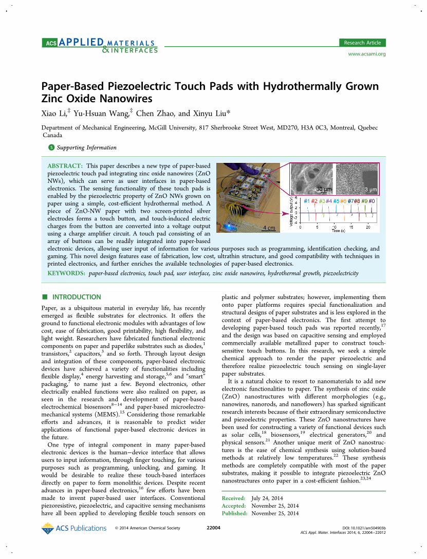
ABSTRACT: This paper describes a new type of paper-basedpiezoelectric touch pad integrating zinc oxide nanowires (ZnONWs), which can serve as user interfaces in paper-basedelectronics. The sensing functionality of these touch pads isenabled by the piezoelectric property of ZnO NWs grown onpaper using a simple, cost-efficient hydrothermal method. Apiece of ZnO-NW paper with two screen-printed silverelectrodes forms a touch button, and touch-induced electriccharges from the button are converted into a voltage outputusing a charge amplifier circuit. A touch pad consisting of anarray of buttons can be readily integrated into paper-basedelectronic devices, allowing user input of information for various purposes such as programming, identification checking, andgaming. This novel design features ease of fabrication, low cost, ultrathin structure, and good compatibility with techniques inprinted electronics, and further enriches the available technologies of paper-based electronics.
KEYWORDS: paper-based electronics, touch pad, user interface, zinc oxide nanowires, hydrothermal growth, piezoelectricity
■ INTRODUCTION
Paper, as a ubiquitous material in everyday life, has recentlyemerged as flexible substrates for electronics. It offers theground to functional electronic modules with advantages of lowcost, ease of fabrication, good printability, high flexibility, andlight weight. Researchers have fabricated functional electroniccomponents on paper and paperlike substrates such as diodes,1
transistors,2 capacitors,3 and so forth. Through layout designand integration of these components, paper-based electronicdevices have achieved a variety of functionalities includingflexible display,4 energy harvesting and storage,5,6 and “smart”packaging,7 to name just a few. Beyond electronics, otherelectrically enabled functions were also realized on paper, asseen in the research and development of paper-basedelectrochemical biosensors8−14 and paper-based microelectro-mechanical systems (MEMS).15 Considering those remarkableefforts and advances, it is reasonable to predict widerapplications of functional paper-based electronic devices inthe future.One type of integral component in many paper-based
electronic devices is the human−device interface that allowsusers to input information, through finger touching, for variouspurposes such as programming, unlocking, and gaming. Itwould be desirable to realize these touch-based interfacesdirectly on paper to form monolithic devices. Despite recentadvances in paper-based electronics,16 few efforts have beenmade to invent paper-based user interfaces. Conventionalpiezoresistive, piezoelectric, and capacitive sensing mechanismshave all been applied to developing flexible touch sensors on
plastic and polymer substrates; however, implementing themonto paper platforms requires special functionalization andstructural designs of paper substrates and is less explored in thecontext of paper-based electronics. The first attempt todeveloping paper-based touch pads was reported recently,17
and the design was based on capacitive sensing and employedcommercially available metallized paper to construct touch-sensitive touch buttons. In this research, we seek a simplechemical approach to render the paper piezoelectric andtherefore realize piezoelectric touch sensing on single-layerpaper substrates.It is a natural choice to resort to nanomaterials to add new
electronic functionalities to paper. The synthesis of zinc oxide(ZnO) nanostructures with different morphologies (e.g.,nanowires, nanorods, and nanoflowers) has sparked significantresearch interests because of their extraordinary semiconductiveand piezoelectric properties. These ZnO nanostructures havebeen used for constructing a variety of functional devices suchas solar cells,18 biosensors,19 electrical generators,20 andphysical sensors.21 Another unique merit of ZnO nanostruc-tures is the ease of chemical synthesis using solution-basedmethods at relatively low temperatures.22 These synthesismethods are completely compatible with most of the papersubstrates, making it possible to integrate piezoelectric ZnOnanostructures onto paper in a cost-efficient fashion.23,24
Received: July 24, 2014Accepted: November 25, 2014Published: November 25, 2014
Research Article
www.acsami.org
© 2014 American Chemical Society 22004 DOI: 10.1021/am504903bACS Appl. Mater. Interfaces 2014, 6, 22004−22012

Here, we report a new type of paper-based piezoelectrictouch pad integrating ZnO nanowires (ZnO NWs) as thesensing component. We directly grow ZnO NWs on cellulosepaper using a simple hydrothermal approach and fabricate theZnO-NW-coated paper into single-layer piezoelectric touchbuttons. Finger contact of a touch button induces deformationof the ZnO NWs on paper microfibers and the ZnO-NW-coated paper substrate as a whole, resulting in an electric chargeoutput from the button, which is converted into a measurablevoltage via a charge amplifier circuit. We investigate the effect oflength of ZnO NWs grown on paper on the output of the touchbutton, and calibrate the button output response. We constructan integrated touch pad consisting of ten buttons as input keysas a demonstration device. The paper-based touch padspresented in this work are inexpensive (CAD $0.03 per pad),easy-to-fabricate, ultrathin, lightweight, and easily obtainableand disposable; they will further enrich the available technologyset of paper-based electronics.
■ EXPERIMENTAL PROCEDURESHydrothermal Growth of ZnO NWs on Cellulose Paper. We
grew ZnO NWs on Whatman 3MM chromatography paper (340 μmthick) through a hydrothermal process modified from a previousprotocol.25 We first synthesized ZnO nanoparticles (ZnO NPs) inethanol and added the ZnO NPs to the paper to form a seeding layerof ZnO NPs for subsequent hydrothermal growth of ZnO NWs. Zincacetate dihydrate (ZAD) (20 mL, 4 mM) and sodium hydroxide(NaOH) (20 mL, 4 mM) solutions were respectively prepared inethanol (200 proof) at 70 °C with heavy stirring. Ethanol (20 mL, 200proof) was then added to the ZAD solution, which was later heated inoven at 70 °C for 30 min. After the ZAD and the NaOH solutionscooled to room temperature, the NaOH solution was slowly added
into the ZAD solution with constant stirring, and the mixture wasplaced in oven at 60 °C for 2 h to crystallize the ZnO NPs and form acolloidal seeding solution. Six pieces (26 mm × 26 mm) of oxygen-plasma-treated paper were immersed in the seeding solution for 3 minand dried at 86 °C for 3 min, and the seeding and drying processeswere repeated six times for each paper piece. When drying the paperpieces after dipping, we put them horizontally on a drying rack withsmall supporting pillars and alternated the surface of paper piece thatfaced down, so that each surface had equal times of facing down. Thisleveled out the effect of gravity to draw the seeding solution to thesurface facing down during drying. An aqueous solution of zinc nitratehexahydrate (ZNH) (50 mM) and hexamethylenetetramine (HMTA)(25 mM) was prepared in a 500 mL flask with stopper. For betterefficiency of the ZnO-NW growth, ammonium hydroxide (AH)solution (0.372 M) was added to the growth solution to suppress thehomogeneous nucleation of ZnO NWs.26 AH forms Zn(NH3)n
2+ tobuffer the supply of Zn2+ so that the supersaturation of the ions in thebulk solution could be lowered and the nucleation in bulk solutioncould be suppressed. This solution was preheated in oven at 86 °C for15 min. Three pieces of seeded paper were then dipped into 100 mLof growth solution at 86 °C for growth of 1.5−15 h. After growth, theZnO-NW paper pieces were washed in deionized water and dried inoven at 90 °C.
Fabrication of the Paper-Based Touch Buttons. The three-dimensional cross-section view of a touch button is illustrated inFigure 1c. We selected the Whatman 3 MM chromatography paper,widely used for fabricating microfluidic devices,27,28 to fabricate thetouch buttons, because: (i) its composition of pure cellulose makes thehydrothermal growth of ZnO NWs more reproducible; and (ii) itsrelatively thick structure (340 μm) is mechanically stable and canhence better withstand pressing-induced deformations. Nevertheless,ZnO NWs can also be readily grown on other common papersubstrates (packing paper29 and plain printing paper30), and our touchbutton design, in principle, can be realized on many other types of
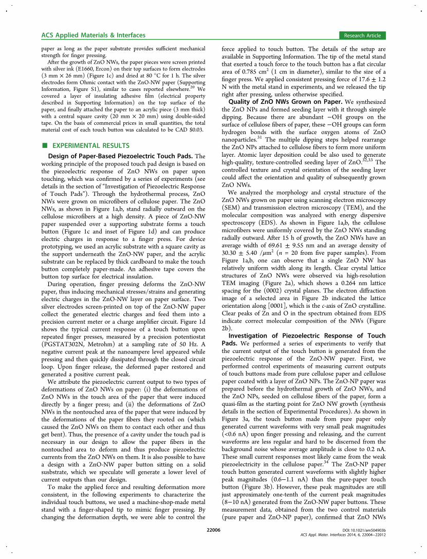
Figure 1. A paper-based piezoelectric touch button with hydrothermally grown ZnO NWs. (a) SEM image of ZnO NWs grown on paper. (b)Zoomed-in SEM image of ZnO NWs grown on cellulose fiber. (c) Schematic view of the touch button. (d) Typical current response of the touchbutton upon repeated finger presses. (insets) A close look at the first pair of peaks and a photo of the device.
ACS Applied Materials & Interfaces Research Article
DOI: 10.1021/am504903bACS Appl. Mater. Interfaces 2014, 6, 22004−22012
22005
paper as long as the paper substrate provides sufficient mechanicalstrength for finger pressing.After the growth of ZnO NWs, the paper pieces were screen printed
with silver ink (E1660, Ercon) on their top surfaces to form electrodes(3 mm × 26 mm) (Figure 1c) and dried at 80 °C for 1 h. The silverelectrodes form Ohmic contact with the ZnO-NW paper (SupportingInformation, Figure S1), similar to cases reported elsewhere.20 Wecovered a layer of insulating adhesive film (electrical propertydescribed in Supporting Information) on the top surface of thepaper, and finally attached the paper to an acrylic piece (3 mm thick)with a central square cavity (20 mm × 20 mm) using double-sidedtape. On the basis of commercial prices in small quantities, the totalmaterial cost of each touch button was calculated to be CAD $0.03.
■ EXPERIMENTAL RESULTS
Design of Paper-Based Piezoelectric Touch Pads. Theworking principle of the proposed touch pad design is based onthe piezoelectric response of ZnO NWs on paper upontouching, which was confirmed by a series of experiments (seedetails in the section of “Investigation of Piezoelectric Responseof Touch Pads”). Through the hydrothermal process, ZnONWs were grown on microfibers of cellulose paper. The ZnONWs, as shown in Figure 1a,b, stand radially outward on thecellulose microfibers at a high density. A piece of ZnO-NWpaper suspended over a supporting substrate forms a touchbutton (Figure 1c and inset of Figure 1d) and can produceelectric charges in response to a finger press. For deviceprototyping, we used an acrylic substrate with a square cavity asthe support underneath the ZnO-NW paper, and the acrylicsubstrate can be replaced by thick cardboard to make the touchbutton completely paper-made. An adhesive tape covers thebutton top surface for electrical insulation.During operation, finger pressing deforms the ZnO-NW
paper, thus inducing mechanical stresses/strains and generatingelectric charges in the ZnO-NW layer on paper surface. Twosilver electrodes screen-printed on top of the ZnO-NW papercollect the generated electric charges and feed them into aprecision current meter or a charge amplifier circuit. Figure 1dshows the typical current response of a touch button uponrepeated finger presses, measured by a precision potentiostat(PGSTAT302N, Metrohm) at a sampling rate of 50 Hz. Anegative current peak at the nanoampere level appeared whilepressing and then quickly dissipated through the closed circuitloop. Upon finger release, the deformed paper restored andgenerated a positive current peak.We attribute the piezoelectric current output to two types of
deformations of ZnO NWs on paper: (i) the deformations ofZnO NWs in the touch area of the paper that were induceddirectly by a finger press; and (ii) the deformations of ZnONWs in the nontouched area of the paper that were induced bythe deformations of the paper fibers they rooted on (whichcaused the ZnO NWs on them to contact each other and thusget bent). Thus, the presence of a cavity under the touch pad isnecessary in our design to allow the paper fibers in thenontouched area to deform and thus produce piezoelectriccurrents from the ZnO NWs on them. It is also possible to havea design with a ZnO-NW paper button sitting on a solidsusbstrate, which we speculate will generate a lower level ofcurrent outputs than our design.To make the applied force and resulting deformation more
consistent, in the following experiments to characterize theindividual touch buttons, we used a machine-shop-made metalstand with a finger-shaped tip to mimic finger pressing. Bychanging the deformation depth, we were able to control the
force applied to touch button. The details of the setup areavailable in Supporting Information. The tip of the metal standthat exerted a touch force to the touch button has a flat circulararea of 0.785 cm2 (1 cm in diameter), similar to the size of afinger press. We applied consistent pressing force of 17.6 ± 1.2N with the metal stand in experiments, and we released the tipright after pressing, unless otherwise specified.
Quality of ZnO NWs Grown on Paper. We synthesizedthe ZnO NPs and formed seeding layer with it through simpledipping. Because there are abundant −OH groups on thesurface of cellulose fibers of paper, these −OH groups can formhydrogen bonds with the surface oxygen atoms of ZnOnanoparticles.31 The multiple dipping steps helped rearrangethe ZnO NPs attached to cellulose fibers to form more uniformlayer. Atomic layer deposition could be also used to generatehigh-quality, texture-controlled seeding layer of ZnO.32,33 Thecontrolled texture and crystal orientation of the seeding layercould affect the orientation and quality of subsequently grownZnO NWs.We analyzed the morphology and crystal structure of the
ZnO NWs grown on paper using scanning electron microscopy(SEM) and transmission electron microscopy (TEM), and themolecular composition was analyzed with energy dispersivespectroscopy (EDS). As shown in Figure 1a,b, the cellulosemicrofibers were uniformly covered by the ZnO NWs standingradially outward. After 15 h of growth, the ZnO NWs have anaverage width of 69.61 ± 9.55 nm and an average density of30.30 ± 5.40 /μm2 (n = 20 from five paper samples). FromFigure 1a,b, one can observe that a single ZnO NW hasrelatively uniform width along its length. Clear crystal latticestructures of ZnO NWs were observed via high-resolutionTEM imaging (Figure 2a), which shows a 0.264 nm latticespacing for the (0002) crystal planes. The electron diffractionimage of a selected area in Figure 2b indicated the latticeorientation along [0001], which is the c-axis of ZnO crystalline.Clear peaks of Zn and O in the spectrum obtained from EDSindicate correct molecular composition of the NWs (Figure2b).
Investigation of Piezoelectric Response of TouchPads. We performed a series of experiments to verify thatthe current output of the touch button is generated from thepiezoelectric response of the ZnO-NW paper. First, weperformed control experiments of measuring current outputsof touch buttons made from pure cellulose paper and cellulosepaper coated with a layer of ZnO NPs. The ZnO-NP paper wasprepared before the hydrothermal growth of ZnO NWs, andthe ZnO NPs, seeded on cellulose fibers of the paper, form aquasi-film as the starting point for ZnO NW growth (synthesisdetails in the section of Experimental Procedures). As shown inFigure 3a, the touch button made from pure paper onlygenerated current waveforms with very small peak magnitudes(<0.6 nA) upon finger pressing and releasing, and the currentwaveforms are less regular and hard to be discerned from thebackground noise whose average amplitude is close to 0.2 nA.These small current responses most likely came from the weakpiezoelectricity in the cellulose paper.34 The ZnO-NP papertouch button generated current waveforms with slightly higherpeak magnitudes (0.6−1.1 nA) than the pure-paper touchbutton (Figure 3b). However, these peak magnitudes are stilljust approximately one-tenth of the current peak magnitudes(8−10 nA) generated from the ZnO-NW paper buttons. Thesemeasurement data, obtained from the two control materials(pure paper and ZnO-NP paper), confirmed that ZnO NWs
ACS Applied Materials & Interfaces Research Article
DOI: 10.1021/am504903bACS Appl. Mater. Interfaces 2014, 6, 22004−22012
22006

are the major source of these repeatable and high-magnitudecurrent waveforms generated from the ZnO-NW paper buttons.Second, we validated that it is the piezoelectricity rather than
the piezoresistivity of ZnO-NW paper that causes the currentoutputs of the touch buttons. When the ZnO-NW paper ispressed, the ZnO NWs standing radially outward on thecellulose fiber will be bent down and contact with each other,which changes the resistivity of the ZnO-NW paper. Thispiezoresistive effect was illustrated by the measurement data ofthe resistance of a ZnO-NW paper button upon finger pressing(Supporting Information, Figure S3). However, we exper-imentally proved that, under our setup for current outputmeasurement (precision potentiostat; no offset voltage appliedduring current measurements), the resistance change of theZnO-NW paper does not induce any current output. Wemeasured the current output of a ZnO-NW paper button uponpresses and delayed releases, during which a finger pressed thetouch button, held the press for a few seconds, and thenreleased it. As shown in Figure 3c, the current output has onlynegative peaks upon pressing and only positive peaks uponreleasing. During the period of holding the press, the resistanceof the ZnO-NW paper changed to a different level (SupportingInformation, Figure S3), but there was no obvious change inthe current level (Figure 3c). On the basis of this observation,we believe that the piezoresistive effect of the ZnO-NW paperdoes not induce obvious current output during touch-buttonoperation; thus, the current peaks are generated by thepiezoelectric effect of the ZnO-NW paper. During pressing
and releasing, the piezoelectric charges were dissipated viacurrent flows through the measurement circuit; thus, thepiezoelectric current diminished quickly when the press andreleas were completed. As a control experiment, we also usedthe same experimental setup to measure the press-inducedcurrent output of a touch button made from cellulose papercoated with carbon ink (Supporting Information, Figure S4).We have shown previously that carbon ink coated on paper has
Figure 2. Characterization of ZnO NWs grown on paper. (a) TEMimages of a ZnO NW. (inset) An electron diffraction image showingthe lattice orientation along [0001]. (b) Chemical analysis of papersurface after ZnO NW growth using EDS.
Figure 3. Investigation of piezoelectric response of the touch button.(a) Current response of touch buttons made from pure paper uponrepeated finger presses. (b) Current response of touch buttons madefrom ZnO-NP paper upon repeated finger presses. (c) Currentresponse of a ZnO-NW paper touch button during presses anddelayed releases.
ACS Applied Materials & Interfaces Research Article
DOI: 10.1021/am504903bACS Appl. Mater. Interfaces 2014, 6, 22004−22012
22007

an obvious piezoresistive effect upon being deformed.15 Themeasurement data, as shown in Supporting Information, FigureS3, demonstrates that there were no obvious current peaksinduced by the presses. This also proved that the piezoresistiveeffect of the ZnO-NW paper does not lead to current output ofthe touch button.As a further proof of the piezoelectric effect in the ZnO-NW
paper, we took time integrations of the current waveformsduring pressing (negative peaks) and releasing (positive peaks)of the touch button (Supporting Information, Figure S5), andthese integrations quantify the amounts of electric chargesgenerated during pressing and releasing. If we assume elasticdeformations of the ZnO-NW paper, the amounts of chargesgenerated during pressing and releasing should be equal. Ourcalculation results show that the amounts of generated chargesfor each pair of negative and positive current peaks are fairlyclose (Supporting Information, Figure S5). This further testifiesto the piezoelectric effect in the ZnO-NW paper during touchbutton operation. The small deviations in the amounts ofcharges generated during pressing and releasing are possiblydue to small unrecovered deformations of the ZnO-NW paperas well as the background noise. We should point out that,although in some current waveforms the negative and positivepeaks in a pair have different magnitudes, the time integrationresults of the current peaks are still very close. The differentmagnitudes of the positive and negative current peaks arebecause of the different speeds of finger pressing andreleasing.29
On the basis of the above experimental validations, weconcluded that the current output of a ZnO-NW paper buttonmainly results from the piezoelectric response of the ZnO NWsgrown on paper. The ZnO NWs generate the major portion ofthe electric charges that form the output currents.20,29 Since therandomly oriented ZnO NWs on cellulose fibers are bent downand contact each other during pressing, it is possible that aportion of the generated electric charges from different ZnONWs are neutralized upon contact, since the contact areas fromtwo ZnO NWs may have opposite piezoelectric chargesaccumulated upon deformation.35 On the other hand, thepress-induced contacts among different ZnO NWs could alsoprovide additional pathways for transporting piezoelectriccharges and thus enhance the charge-transfer efficiency.21
To fully characterize the piezoelectric properties of the ZnO-NW paper, detailed material characterization will be needed. Inregard to mechanical properties, the Young’s moduli of ZnONW and cellulose are expected to be 52 GPa36 and 130 GPa,37
respectively. A piece of cellulose paper is a network ofinterconnected cellulose microfibers with pores, and its effectiveYoung’s modulus was measured to be just 2 GPa15 (assuminghomogeneity of cellulose paper). When analyzing themechanical deformations, note that the system is a multiscalecomplex structure network involving deformations of structuresof different sizes, orientations, and connections. In regard toelectrical property, piezoelectric coefficient is an importantparameter, and its measurement requires sophisticatedexperimental setup. We did not measure the piezoelectriccoefficient of ZnO NWs we synthesized due to theexperimental constraints. According to a previous study onsingle ZnO NWs, the effective piezoelectric coefficient (d33) ofZnO NW grown in the orientation of [0001] can be estimatedas 3−12 nm/V.38 To scrutinize the deformation of individualZnO NWs on paper under finger touch, multiscale mechanicalmodeling of the hierarchical structure of ZnO NWs on cellulose
microfiber network is required. The reasons are the nanowiresare not well-aligned on randomly woven paper microfibers, andthe deformation of individual ZnO NWs varies across the entirepiece of paper.
Effect of ZnO-NW Growth Percentage on DeviceCurrent Response. It is a common observation that, givenextended growth time, ZnO NWs grow longer.26,39 Wemeasured the weight of paper pieces before and after growth.We defined the growth percentage of ZnO NWs as weightincrease of the paper pieces (vs weight before growth) inpercentage: 100% × (weight after growth − weight beforegrowth)/weight before growth. We investigated the effect ofZnO-NW growth percentage on the device current output. Inour experiments, the paper pieces were weighed in dry formbefore and after ZnO-NW growth. Similar with otherreports,26,39 we noted that the ZnO NWs grew quickly in thefirst 3 h, and the growth slowed down after that and almoststopped after 15 h. This growth profile can be explained by thegradual depletion of chemicals in the growth solution. Thegrowth percentages after 1.5, 3, and 15 h are 19.7 ± 0.5%, 30.3± 1.2%, and 40.3 ± 0.5%, respectively (n = 3). Higher growthpercentages can be achieved by carrying out the growth for alonger period of time and refreshing the growth solutionconstantly.18
We measured current outputs of the touch buttons, withZnO-NW growth percentages of 19.7% (1.5 h of growth),30.3% (3 h of growth), and 40.3% (15 h of growth). As shownin Figure 4a, the average magnitude of negative current peaksshows an obvious increasing trend with the growth percentage.We opted not to present the data of average current magnitudevs ZnO-NW length, because it is hard to clearly identify theroot of ZnO NWs that are grown on non-flat and not-smoothcellulose surface. That is also the major reason we resorted tothe parameter, growth percentage, which is more convenientand accurate to indirectly quantify the length of ZnO NWs.On the basis of the discussions in the section of
“Investigation of Piezoelectric Response of Touch Pads”, wespeculate two possible reasons for the increased current outputswith higher growth percentages. (i) Longer ZnO NWs deflectmore under the same pressing force and thus generate moreelectric charges. (ii) Longer ZnO NWs have higher chance tocontact each other when the cellulose fiber they stand on isbent; thus, longer ZnO NWs may gain more electronicpathways for charge transport. Although the results imply that alonger growth time leads to a higher growth percentage andlonger ZnO NWs, along with higher current output, note thatthere are limitations to elevating piezoelectric output byincreasing growth time or ZnO-NW length. First, anotherresearch has showed there is an optimal ratio of ZnO NWlength to width that generates the highest piezoelectricresponse.40 Second, over long time growth, ZnO NWs tendto fuse at their tips, which interferes with their growth.
Effect of Pressing Force on Device Current Response.We also investigated the current response of touch buttons atdifferent pressing force levels. Hard and gentle presses deformthe ZnO-NW paper at different rates and to different extents,thus resulting in different current outputs. We adjusted thepressing force applied to the touch buttons and measured theircurrent outputs. As shown in Figure 4b, the average magnitudeof negative current peaks increases linearly with the pressingforce, with a sensitivity of 0.57 nA/N. If a more sensitiveresponse of the touch button is desired, one can choose athinner and thus more flexible paper substrate and adopt a
ACS Applied Materials & Interfaces Research Article
DOI: 10.1021/am504903bACS Appl. Mater. Interfaces 2014, 6, 22004−22012
22008

higher ZnO-NW growth percentage in device preparation. Thelinear fitting in Figure 4b shows that an initial force (2.60 N,obtained from the linear fitting equation) is needed before acurrent output can be measured, which represents the cutoffforce value of the device’s dead zone. One can reduce thiscutoff value by using a thinner piece of paper for constructingthe touch button, which is more compliant to deform.In the experiments, the metal tip on the metal stand we used
has a flat circular area (1 mm in diameter) with a similar sizewith a typical human finger. We experimentally verified that apress by the metal post and a press by a similarly sized humanfinger, both with the same level of applied force, generatedpiezoelectric current outputs from the same button with adiscrepancy of <10%. It is reasonable to predict that when thearea and shape of the metal post change, the amount ofdeformed ZnO NWs and the stress/strain distribution in theZnO-NW paper will change accordingly. This will definitelylead to the change in the piezoelectric current outputs. Toreduce the experimental complexity, we did not investigate theeffect of the contact shape and the area on the touch buttonoutput.Durability Testing. Performance degradation after re-
peated operations could be a concern if the paper-based
touch buttons are designed for long-term use. We tested thedevice durability through repeated pressing of a touch buttonmade from paper with a ZnO-NW growth percentage of 30.3%.The button was continuously pressed 2000 times using themetal stand at a high force level of 17.6 ± 1.2 N. After every200 presses, the current output was measured 10 times tocalculate the average. As shown in Figure 5, the averagemagnitude of negative current peaks decreased gradually duringthe first 600 presses and started to stabilize after that.
We observed two causes associated with the outputdegradation. (i) Repeated presses resulted in unrecoverable(inelastic) deformation of the paper, which we started toobserve after the first 100 presses. This irreversible deformationcaused stiffening in the suspended paper structure, decreasedthe deformation/strain induced by the subsequent presses, andthus lowered the current output. (ii) Repeated presses alsopermanently bent down the ZnO NWs on paper, making themless stressed in the subsequent presses. This was revealedthrough SEM imaging of the ZnO NWs after 600 presses (insetin Figure 5). The current output stabilized after 600 presses,possibly because the suspended paper reached the limit ofinelastic deformation and mainly underwent elastic deformationafterward. After 2000 presses, the touch button still operatedresponsively, and no mechanical damage was observed on thepaper button. In application scenarios where extended uses aretargeted, the paper touch buttons can be preloaded to reachstabilized performance.
Development and Operation of a Ten-Key Touch Pad.After characterization of the touch button, we constructed atouch pad by arraying 10 numbered buttons (Figure 6) on anacrylic frame. The touch pad also includes a 10-channel chargeamplifier circuit (Supporting Information, Figure S6; CAD $1.4per channel ) for converting electric charges from the buttonsinto voltage outputs, a microcontroller circuit (ATxmega32A4,ATMEL) for measuring the voltage outputs, and 11 light-emitting diodes (LEDs; 10 blue and one green) for touch-responsive displays. Figure 6a shows the voltage outputs fromthe 10 touch buttons when they were pressed sequentially by ahuman operator. The positive peak amplitudes of the voltageoutputs vary across different buttons, which could be attributedto the different levels of pressing and environmental noisescoupled into the 10 channels of the charge amplifier circuit.The microcontroller was programmed to recognize fingerpresses by detecting the positive voltage peaks from the touchbuttons based on a threshold value. Upon recognition of finger
Figure 4. Experimental results of average negative current peaks vsgrowth percentage and force applied. (a) Experimental results ofaverage negative current peaks vs ZnO-NW growth percentage (n = 3devices). ZnO NWs were grown for 1.5, 3, and 15 h, yielding 20%,30%, and 40% weight growth, respectively. (b) Experimental results ofaverage negative current peaks vs pressing force (n = 3 devices; 10measurements per deformation), collected from devices with a growthpercentage of 40%. Equation of the linear regression: y = 0.57x − 1.48,(R2 = 0.937).
Figure 5. Experimental results of average negative current peak vsnumber of presses (n = 10 measurements every 200 presses). (inset)An SEM image of a touch pad after 600 presses.
ACS Applied Materials & Interfaces Research Article
DOI: 10.1021/am504903bACS Appl. Mater. Interfaces 2014, 6, 22004−22012
22009

pressing on a specific button, a corresponding blue LED was litby the microcontroller (Figure 6b and the video of SupportingInformation, 2). To highlight the potential use of our touchpads in paper-based electronics where input of information isneeded, we demonstrated the input of a six-digit numeric codeon the touch pad. The microcontroller was programmed tocompare the inputted code with the preset one and activate thegreen LED when there was a match (Figure 6c and the video ofSupporting Information, 3).
■ DISCUSSIONAdvantages of the Developed Touch Pad. The addition
of touch-sensing capabilities to common paper substrates is ofprimary importance to developing monolithic paper-basedelectronic devices with touch user interfaces. In this research,we demonstrated a new design of paper-based piezoelectrictouch pads that serve as interfaces for user input of information.Our touch pad design has five useful characteristics for uses inpaper-based electronics. (i) The piezoelectric sensing principleis, in principle, applicable to most types of paper substrates.The hydrothermal synthesis of ZnO NWs can be performed onvirtually any paper substrates with proper mechanical stability,making our design useful for many paper-based electronicdevices involving different paper substrates. (ii) The design justneeds a single layer of paper, which simplifies the deviceassembly. (iii) The device is simple-to-fabricate, fairly low-cost(CAD $0.03 per button), and does not require sophisticatedmicrofabrication facilities. (iv) The device fabrication process iscompatible with existing techniques for constructing electroniccircuits on paper substrates (e.g., inkjet and screening printing).The hydrothermal growth of ZnO NWs is performed in amoderate chemical solution at relatively low temperatures (50−100 °C), which does not substantially change the chemical and
mechanical properties of the paper substrate and hence permitssubsequent fabrication of electronic components on the samepaper substrate. (v) The hydrothermal synthesis of ZnO-NWsis highly selective and spatially guided by the seeding layer ofZnO NPs. One can easily pattern the seeding layer via inkjetprinting of the ZnO-NP solution and conduct selective growthof ZnO NWs on paper with micrometer resolution(determined by the resolution of inkjet printing). This willpotentially lead to more versatile designs of paper-based touchsensors.
Advantages of Using Paper as Electronic Substrate. Itis possible to hydrothermally grow ZnO NWs on plasticsubstrates,41 which represents another type of commonmaterials for constructing flexible electronic devices. Comparedto plastics, paper has the following advantages for use as anelectronic substrate. (i) Paper is biodegradable, readilydisposable by incineration, and thus more environmentallyfriendly than plastics. (ii) According to a previous compar-ison,16 paper has lower cost (∼EUR €0.001 per dm2) than mostplastics (e.g., polyethylene terephthalate: ∼EUR €0.02 per dm2;polyimide: ∼EUR €0.3 per dm2). (iii) There exist mature mass-production techniques for manufacturing paper materials (e.g.,printing, folding, and cutting) that could be adapted tomanufacturing paper-based electronic products. (iv) As asubstrate for growing ZnO NWs, the porous structure ofcellulose paper provides a higher surface-to-volume ratio thanplastic substrates, which allows the growth of more ZnO NWsper unit area of substrate.
New Contributions of the Presented Work. Althoughprevious work has demonstrated the use of ZnO-NW paper forenergy harvesting,29 we believe this research is distinct inseveral important aspects. First, this work is aimed towardinventing a new type of user touch interface for paper-basedelectronics, which is a different application from the previouswork.29 Our research is the first demonstration of paper-basedpiezoelectric touch sensor. Second, the procedures of growingZnO NWs on paper in this research are different from those ofprevious work.29 For example, the previous work29 sputteredZnO NPs on paper, while we prepared ZnO-NP colloidalsolution and dipped paper into it for seeding, which does notrequire sophisticated equipment. For hydrothermal synthesis ofZnO NWs, we utilized ammonium hydroxide as an assistantchemical to suppress the homogeneous nucleation of ZnO insolution, which leads to thinner ZnO NWs (69.61 nm after 15h of growth) than that (100−200 nm after 3 h of growth) inthe previous work.29 Third, the form of deformation of theZnO-NW paper is different in our work than that of previouswork.29 The previous design29 used a piece of paper as a straingauge (attached to a plastic cantilever beam), whichexperienced tensile or compressive strains during operation.We formed a touch button from a suspended ZnO-NW paper,and the finger touching induced both bending and stretching ofthe paper. This difference in form of deformation led todifferent quantitative relationships of the current output versusthe applied load. Fourth, we undertook a series of investigationson the piezoelectric sensing mechanism of ZnO-NW paper,which are new technical contributions. We calibrated thecurrent output as a function of the amount of ZnO NWs grownon paper (reflected by the growth weight percentage), whichprovides guidelines for device design. We tested the perform-ance degradation of the touch button upon repeated pressing,which is a necessary test for constructing reliable paper-basedsensors. We also developed a simple charge amplifier circuit for
Figure 6. Voltage output and snapshot of key pad. (A)Voltage outputsfrom 10 number keys while being dialed. (b) The corresponding blueLED lighting when the number key is pressed. (c) The green LEDlighting when a preprogrammed password is entered correctly.
ACS Applied Materials & Interfaces Research Article
DOI: 10.1021/am504903bACS Appl. Mater. Interfaces 2014, 6, 22004−22012
22010

converting the piezoelectric charge output into a measurablevoltage output.Understanding the Detailed Physical Mechanisms.We
dedicated a series of experiments to understand the mechanismof the current responses from the developed touch pads. Weobtained the following experimental observations for ourcurrent touch pad design: (i) ZnO NWs grown on papermade the major contribution to the output current peaks; (ii)the press-induced piezoresistive effect of ZnO-NW paper didnot lead to obvious current response of the touch pad; and (iii)the piezoelectric charges generated during a finger press andsubsequent release of the touch button are equal (smalldeviations exist in experiments due to small uncovereddeformations and background noise of the buttons). Theseobservations led to our conclusion that the current outputsfrom the touch pads arise from the piezoelectric effect of theZnO NWs on paper. These investigations also reveal a highlyinteresting research topic to explore in future on theoreticalmodeling and computational simulation of the mechanicaldeformation and corresponding piezoelectronics of thehierarchical structure of ZnO NWs on interwoven cellulosemicrofibers, which will help us better understand the chargegeneration and transfer in ZnO-NW paper.Potential Improvements. We developed touch pad
prototypes for proof-of-concept demonstrations, and furtherengineering improvements can be performed to enhance thedevice performance or extend the functionality. (i) Theconsistency of output voltages from different touch buttonscan be further improved through better control of the ZnOgrowth consistency and environmental noises coupled into thecharge amplifier circuit. (ii) Selective growth of ZnO-NW andcorresponding patterning of conductive inks (as electrodes) canbe achieved, via techniques such as inkjet printing, to formaddressable arrays of touch sensing “pixels” with potentiallysmaller footprint. This will further increase the level of deviceintegration. The major limitations of reducing the sensing pixelsize include the patterning resolution of the hydrothermallygrown ZnO NWs (mainly determined by inkjet printingresolution of the seeding solution) and the size-relatedlimitation of the piezoelectric current output of each patternedsensing pixel (the smaller the pixel, the lower the outputcurrent). (iii) The whole charge-amplifier circuit can beintegrated onto the same paper substrate using existing circuitfabrication techniques in paper-based electronics.15,16
Potential Applications. Besides the demonstrated usagesof these touch pads, we expect many other interestingapplications. For instance, the single-layer touch pad designcan be integrated into many interactive electronic paperproducts such as business and greeting cards, boarding passes,intelligent magazines. Creative cutting and folding of paperpatterned with ZnO NWs can make “smart” paper toys thatrespond to physical interactions from users (e.g., pressing,bending, and accelerating). The piezoelectric mechanism forphysical sensing could also enable the development of low-costdisposable force sensors and accelerometers.
■ CONCLUSIONThis paper reported a new design of paper-based piezoelectrictouch pads integrating ZnO NWs, representing an inexpensivesolution to developing novel user interfaces for paper-basedelectronics. We hydrothermally grew ZnO NWs on cellulosepaper and fabricated the ZnO-NW paper into piezoelectrictouch buttons. The ZnO-NW paper button is responsive to
finger pressing and generates electric charges, which are thenconverted into a voltage signal using a charge amplifier circuit.We fully characterized the output performance of the touchbutton and examined the device durability during 2000 cyclesof pressing. We constructed an integrated touch pad with 10touch buttons and demonstrated its potential use in user−device interactions. We believe that this technology has asignificant potential for use in paper-based electronic platformsto improve interactive user experience and enable other touch-sensing-based functionalities.
■ ASSOCIATED CONTENT*S Supporting InformationFigures mentioned in the section of “Investigation ofPiezoelectric Response of Touch Pads” and videos taken withthe ten-key touch pad. This material is available free of chargevia the Internet at http://pubs.acs.org.
■ AUTHOR INFORMATIONCorresponding Author*E-mail: [email protected] Contributions‡These authors contributed equally to this work.NotesThe authors declare no competing financial interest.
■ ACKNOWLEDGMENTSThis research was supported by Natural Sciences andEngineering Research Council of Canada (NSERC) (GrantNo. RGPIN 418553-12), Canada Foundation for Innovation(Grant No. CFI-LOF 30316), and McGill University (GrantNo. 120536). The authors also acknowledge financial supportsfrom the Canadian Research Chairs Program (Grant No.237293) and the McGill Chwang-Seto Faculty ScholarshipProgram (to X.L.) (Grant No. 234304), the McGill SummerUndergraduate Research in Engineering (SURE) Program (toY.H.W.), and the NSERC-CREATE Training Program inIntegrated Sensor Systems (to X.L. and C.Z.).
■ REFERENCES(1) Lilja, K. E.; Backlund, T. G.; Lupo, D.; Hassinen, T.; Joutsenoja,T. Gravure Printed Organic Rectifying Diodes Operating at HighFrequencies. Org. Electron. 2009, 10, 1011−1014.(2) Kurra, N.; Dutta, D.; Kulkarni, G. U. Field Effect Transistors andRC Filters from Pencil-Trace on Paper. Phys. Chem. Chem. Phys. 2013,15, 8367−8372.(3) Jung, M.; Kim, J.; Noh, J.; Lim, N.; Lim, C.; Lee, G.; Kim, J.;Kang, H.; Jung, K.; Leonard, A. D.; Tour, J. M.; Cho, G. All-Printedand Roll-to-Roll-Printable 13.56-MHz-Operated 1-bit RF Tag onPlastic Foils. IEEE Trans. Electron Devices 2010, 57, 571−580.(4) Andersson, P.; Nilsson, D.; Svensson, P. O.; Chen, M. X.;Malmstrom, A.; Remonen, T.; Kugler, T.; Berggren, M. Active MatrixDisplays Based on All-Organic Electrochemical Smart Pixels Printedon Paper. Adv. Mater. 2002, 14, 1460−1464.(5) Kumar, A.; Gullapalli, H.; Balakrishnan, K.; Botello-Mendez, A.;Vajtai, R.; Terrones, M.; Ajayan, P. M. Flexible ZnO-CelluloseNanocomposite for Multisource Energy Conversion. Small 2011, 7,2173−2178.(6) Hu, L.; Choi, J. W.; Yang, Y.; Jeong, S.; La Mantia, F.; Cui, L. F.;Cui, Y. Highly Conductive Paper for Energy-Storage Devices. Proc.Natl. Acad. Sci. U. S. A. 2009, 106, 21490−21494.(7) Unander, T.; Nilsson, H. E. Characterization of Printed MoistureSensors in Packaging Surveillance Applications. IEEE. Sens. J. 2009, 9,922−928.
ACS Applied Materials & Interfaces Research Article
DOI: 10.1021/am504903bACS Appl. Mater. Interfaces 2014, 6, 22004−22012
22011

(8) Zang, D.; Ge, L.; Yan, M.; Song, X.; Yu, J. ElectrochemicalImmunoassay on a 3D Microfluidic Paper-Based Device. Chem.Commun. 2012, 48, 4683−4685.(9) Delaney, J. L.; Hogan, C. F.; Tian, J.; Shen, W. ElectrogeneratedChemiluminescence Detection in Paper-Based Microfluidic Sensors.Anal. Chem. 2011, 83, 1300−1306.(10) Liu, H.; Crooks, R. M. Paper-Based Electrochemical SensingPlatform with Integral Battery and Electrochromic Read-Out. Anal.Chem. 2012, 84, 2528−2532.(11) Thom, N. K.; Yeung, K.; Pillion, M. B.; Phillips, S. T. FluidicBatteries” As Low-Lost Sources of Power in Paper-Based MicrofluidicDevices. Lab Chip 2012, 12, 1768−1770.(12) Nie, Z.; Nijhuis, C. A.; Gong, J.; Chen, X.; Kumachev, A.;Martinez, A. W.; Narovlyansky, M.; Whitesides, G. M. ElectrochemicalSensing in Paper-Based Microfluidic Devices. Lab Chip 2010, 10,477−83.(13) Zhao, C.; Thuo, M. M.; Liu, X. A Microfluidic Paper-BasedElectrochemical Biosensor Array for Multiplexed Detection ofMetabolic Biomarkers. Sci. Technol. Adv. Mater. 2013, 14, 054402.(14) Nie, Z.; Deiss, F.; Liu, X.; Akbulut, O.; Whitesides, G. M.Integration of Paper-Based Microfluidic Devices with CommercialElectrochemical Readers. Lab Chip 2010, 10, 3163−3169.(15) Liu, X.; Mwangi, M.; Li, X.; O’Brien, M.; Whitesides, G. M.Paper-Based Piezoresistive MEMS Sensors. Lab Chip 2011, 11, 2189−2196.(16) Tobjork, D.; Osterbacka, R. Paper Electronics. Adv. Mater. 2011,23, 1935−1961.(17) Mazzeo, A. D.; Kalb, W. B.; Chan, L.; Killian, M. G.; Bloch, J. F.;Mazzeo, B. A.; Whitesides, G. M. Paper-Based, Capacitive Touch Pads.Adv. Mater. 2012, 24, 2850−2856.(18) Law, M.; Greene, L. E.; Johnson, J. C.; Saykally, R.; Yang, P.Nanowire Dye-Sensitized Solar Cells. Nat. Mater. 2005, 4, 455−459.(19) Wei, A.; Sun, X. W.; Wang, J. X.; Lei, Y.; Cai, X. P.; Li, C. M.;Dong, Z. L.; Huang, W. Enzymatic Glucose Biosensor Based on ZnONanorod Array Grown by Hydrothermal Decomposition. Appl. Phys.Lett. 2006, 89, 123902.(20) Wang, Z. L.; Song, J. H. Piezoelectric Nanogenerators Based onZinc Oxide Nanowire Arrays. Science 2006, 312, 242−246.(21) Xiao, X.; Yuan, L.; Zhong, J.; Ding, T.; Liu, Y.; Cai, Z.; Rong, Y.;Han, H.; Zhou, J.; Wang, Z. L. High-Strain Sensors Based on ZnONanowire/Polystyrene Hybridized Flexible FIlms. Adv. Mater. 2011,23, 5440−5444.(22) Ko, H.; Zhang, Z. X.; Takei, K.; Javey, A. Hierarchical PolymerMicropillar Arrays Decorated with ZnO Nanowires. Nanotechnology2010, 21, 295305.(23) Baruah, S.; Jaisai, M.; Imani, R.; Nazhad, M. M.; Dutta, J.Photocatalytic Paper Using Zinc Oxide Nanorods. Sci. Technol. Adv.Mater. 2010, 11, 055002.(24) Manekkathodi, A.; Lu, M. Y.; Wang, C. W.; Chen, L. J. DirectGrowth of Aligned Zinc Oxide Nanorods on Paper Substrates forLow-Cost Flexible Electronics. Adv. Mater. 2010, 22, 4059−4063.(25) Vayssieres, L. Growth of Arrayed Nanorods and Nanowires ofZnO from Aqueous Solutions. Adv. Mater. 2003, 15, 464−466.(26) Xu, C. K.; Shin, P.; Cao, L. L.; Gao, D. Preferential Growth ofLong ZnO Nanowire Array and Its Application in Dye-Sensitized SolarCells. J. Phys. Chem. C 2010, 114, 125−129.(27) Liu, X. Y.; Cheng, C. M.; Martinez, A. W.; Mirica, K. A.; Li, X. J.;Phillips, S. T.; Mascarenas, M.; Whitesides, G. M. In A PortableMicrofluidic Paper-Based Device for ELISA, IEEE 24th InternationalConference on Micro Electro Mechanical Systems, Cancun, Mexico,Jan 23−27; IEEE: Piscataway, NJ, 2011; pp 75−78.(28) Li, X.; Liu, X. Fabrication of Three-Dimensional MicrofluidicChannels in a Single Layer of Cellulose Paper. Microfluid. Nanofluid.2014, 16, 819−827.(29) Qiu, Y.; Zhang, H.; Hu, L.; Yang, D.; Wang, L.; Wang, B.; Ji, J.;Liu, G.; Liu, X.; Lin, J.; Li, F.; Han, S. Flexible PiezoelectricNanogenerators Based on ZnO Nanorods Grown on Common PaperSubstrates. Nanoscale 2012, 4, 6568−6573.
(30) Gullapalli, H.; Vemuru, V. S.; Kumar, A.; Botello-Mendez, A.;Vajtai, R.; Terrones, M.; Nagarajaiah, S.; Ajayan, P. M. FlexiblePiezoelectric ZnO-Paper Nanocomposite Strain Sensor. Small 2010, 6,1641−1646.(31) Jaisai, M.; Baruah, S.; Dutta, J. Paper Modified with ZnONanorods - Antimicrobial Studies. Beilstein J. Nanotechnol. 2012, 3,684−691.(32) Tynell, T.; Karppinen, M. Atomic Layer Deposition of ZnO: AReview. Semicond. Sci. Technol. 2014, 29, 043001−043015.(33) Solis-Pomar, F.; Martinez, E.; Melendrez, M. F.; Perez-Tijerina,E. Growth of Vertically Aligned ZnO Nanorods Using Textured ZnOFilms. Nanoscale Res. Lett. 2011, 6, 524−534.(34) Kim, J.; Yun, S.; Ounaies, Z. Discovery of Cellulose As a SmartMaterial. Macromolecules 2006, 39, 4202−4206.(35) Wang, Z. L. Towards Self-Powered Nanosystems: FromNanogenerators to Nanopiezotronics. Adv. Funct. Mater. 2008, 18,3553−3567.(36) Bai, X. D.; Gao, P. X.; Wang, Z. L.; Wang, E. G. Dual-modemechanical resonance of individual ZnO nanobelts. Appl. Phys. Lett.2003, 82, 4806−4808.(37) Vincent, J. F. V. From cellulose to cell. J. Exp. Biol. 1999, 202,3263−3268.(38) Zhu, R.; Wang, D. Q.; Xiang, S. Q.; Zhou, Z. Y.; Ye, X. Y.Piezoelectric characterization of a single zinc oxide nanowire using ananoelectromechanical oscillator. Nanotechnology 2008, 19, 285712−285716.(39) Qiu, J. J.; Li, X. M.; Zhuge, F. W.; Gan, X. Y.; Gao, X. D.; He, W.Z.; Park, S. J.; Kim, H. K.; Hwang, Y. H. Solution-Derived 40 μmVertically Aligned ZnO Nanowire Arrays As Photoelectrodes in Dye-Sensitized Solar Cells. Nanotechnology 2010, 21, 195602−195610.(40) Riaz, M.; Song, J.; Nur, O.; Wang, Z. L.; Willander, M. Study ofthe Piezoelectric Power Generation of ZnO Nanowire Arrays Grownby Different Methods. Adv. Funct. Mater. 2011, 21, 628−633.(41) Gao, P. X.; Song, J. H.; Liu, J.; Wang, Z. L. Nanowirepiezoelectric nanogenerators on plastic substrates as flexible powersources for nanodevices. Adv. Mater. 2007, 19, 67−72.
ACS Applied Materials & Interfaces Research Article
DOI: 10.1021/am504903bACS Appl. Mater. Interfaces 2014, 6, 22004−22012
22012