page 1 • may 2009 feature article rf/microwave …€¦ · · 2015-05-12in modern rf/microwave...
TRANSCRIPT

PAGE 1 • MAY 2009 www.MPdiGEst.coMFEATURE ARTICLE
Introduction
Solid state switches are ubiquitous in modern RF/microwave systems. They are utilized to control signal
flows, select signal sources and for many other applications. These switches are implemented either with positive-intrinsic-negative (PIN) diodes or with field effect transistors (FETs) such as pseudomor-phic high electron mobility transistors (pHEMTs), each of which offers relative advantages and disadvantages. Part 1 of this article includes an overview of RF/microwave switches, theory of operation for PIN diodes and some representative PIN diode switch circuits. In Part 2 we will discuss more PIN diode switch con-figurations, the theory of operation for FETs, some representative RF/microwave FET switch topologies, the relative advan-tages of PIN and FET switches and some criteria by which one of these technologies may be selected over the other for switch applications.
RF/Microwave Solid State Switches OverviewRF/microwave switches utilize variable impedance circuit elements to direct the flow of signals. A switch either allows a signal to propagate through a specific signal path or it blocks the signal from fol-lowing this path. In an ideal switch, circuit paths are either closed via an ideal conduc-tor with 0 Ω impedance or opened by an ideal open circuit with infinite impedance. Modern semiconductor elements cannot quite meet those ideal impedance values, but they can come sufficiently close to pro-duce excellent switch performance.
Reflective or Absorptive?Switches in the RF realm can be implement-ed as reflective or absorptive structures.
An ideal reflective switch places either an open circuit in cascade with a signal path (Figure 1), or a short circuit across the signal path (Figure 2).
These two extreme impedances produce maximum mismatch of impedance, which produces reflection of the entire incident signal back to its source.
An ideal absorptive switch (sometimes called a “matched switch”) produces iso-lation by placing a termination whose resistance is exactly equal to the charac-teristic impedance, Z0, of the transmis-sion line across the transmission line as shown in Figure 3. In this case, all of the incident signal energy is absorbed by the terminating resistance and dissipated as
heat, leaving no remaining energy to be reflected back to the signal source. In the other state, the termination is disconnected from the transmission line, thereby allow-ing all of the incident energy to propagate through the switch.
Common Switch ConfigurationsSwitches may be implemented in many configurations. These configurations are described in terms of the number of poles
and the number of throws implemented in the switch. The number of poles describes the number of signal paths controlled by the switch. The number of throws indicates the number of potential directions into which a pole may be placed. For example, the simplest switch configuration is a single pole, single throw (SPST) switch. This con-figuration has one signal path which can either be completed by the switch or inter-rupted by the switch. A single pole double throw switch (SPDT or SP2T) can connect a single transmission line to either of two other transmission lines. The number of poles and throws, and the combinations thereof, is unlimited in the ideal sense, but has practical limitations that will be described later in this paper.
Ideal vs. Practical SwitchesIn practical solid state RF/microwave switches, it is not possible to produce a perfect open impedance nor a perfect short circuit. Consequently, there is always some small amount of incident signal that is absorbed by the switch and a bit more reflected by the switch’s nonideal imped-ance when the switch is in the state in which it should ideally pass all incident signal energy. This small reduction in sig-nal amplitude is known as insertion loss (IL) and is typically described in terms of decibels (dB). Insertion loss is simply the ratio of the output power to the input power.
Likewise, there is always some small amount of energy that propagates past the switch when it is in the state in which an ideal switch should produce infinite isolation. The measurement of this char-acteristic is known as isolation and is also described in terms of dB. Isolation is also the ratio of the output power to the input power.
Multiple semiconductor elements can be used in a single switch to increase the isolation that the switch produces. Often, these elements are placed in series with the signal path and in shunt with the path. Absorptive switches typically include mul-tiple switching elements: some to complete or interrupt the signal path and others to disconnect or connect the termination resistance to the signal path.
PIN Diode Theory of Operation1
The PIN diode is a current controlled resis-tor at radio and microwave frequencies. It is a semiconductor diode in which a high-resistivity intrinsic I region is sandwiched between a p-type and an n-type region as
RF/Microwave Solid State Switchesby Rick Cory, Skyworks Solutions, Inc.
Figure 1: Transmission System with Series Open Discontinuity
Figure 2: Transmission System with Shunt Short Discontinuity
Figure 3: Transmission System with Absorptive Switch
PAGE 2 • MAY 2009 www.MPdiGEst.coMFEATURE ARTICLE
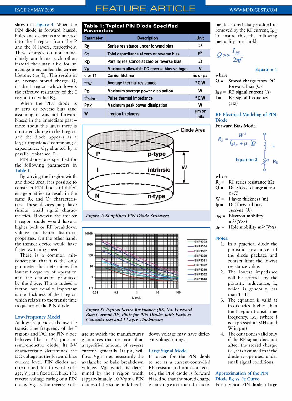
shown in Figure 4. When the PIN diode is forward biased, holes and electrons are injected into the I region from the P and the N layers, respectively. These charges do not imme-diately annihilate each other; instead they stay alive for an average time, called the carrier lifetime, τ or TL. This results in an average stored charge, Q, in the I region which lowers the effective resistance of the I region to a value RS.
When the PIN diode is at zero or reverse bias (and assuming it was not forward biased in the immediate past – more about this later) there is no stored charge in the I region and the diode appears as a larger impedance comprising a capacitance, CT, shunted by a parallel resistance, RP.
PIN diodes are specified for the following parameters in Table 1.
By varying the I region width and diode area, it is possible to construct PIN diodes of differ-ent geometries to result in the same RS and CT characteris-tics. These devices may have similar small signal charac-teristics. However, the thicker I region diode would have a higher bulk or RF breakdown voltage and better distortion properties. On the other hand, the thinner device would have faster switching speed.
There is a common mis-conception that τ is the only parameter that determines the lowest frequency of operation and the distortion produced by the diode. This is indeed a factor, but equally important is the thickness of the I region which relates to the transit time frequency of the PIN diode.
Low-Frequency ModelAt low frequencies (below the transit time frequency of the I region) and DC, the PIN diode behaves like a PN junction semiconductor diode. Its I-V characteristic determines the DC voltage at the forward bias current level. PIN diodes are often rated for forward volt-age, VF, at a fixed DC bias. The reverse voltage rating of a PIN diode, VR, is the reverse volt-
age at which the manufacturer guarantees that no more than a specified amount of reverse current, generally 10 µA, will flow. VR is not necessarily the avalanche or bulk breakdown voltage, VB, which is deter-mined by the I region width (approximately 10 V/µm). PIN diodes of the same bulk break-
down voltage may have differ-ent voltage ratings.
Large Signal ModelIn order for the PIN diode to act as a current-controlled RF resistor and not as a recti-fier, the PIN diode is forward biased so that the stored charge is much greater than the incre-
mental stored charge added or removed by the RF current, IRF. To insure this, the following inequality must hold:
Equation 1where Q = Stored charge from DC forward bias (C)IRF = RF signal current (A)f = RF signal frequency (Hz)
RF Electrical Modeling of PIN DiodeForward Bias Model
Equation 2
whereRS = RF series resistance (Ω)Q = DC stored charge = IF × τ (C)W = I layer thickness (m)IF = DC forward bias current (A)mN = Electron mobility m2/(V×s)mP = Hole mobility m2/(V×s)
Notes:In a practical diode the 1. parasitic resistance of the diode package and contact limit the lowest resistance value.The lowest impedance 2. will be affected by the parasitic inductance, L, which is generally less than 1 nH.The equation is valid at 3. frequencies higher than the I region transit time frequency, i.e., (where f is expressed in MHz and W in µm)The equation is valid only 4. if the RF signal does not affect the stored charge, i.e., it is assumed that the diode is operated under small signal conditions.
Approximation of the PIN Diode RS vs. IF CurveFor a typical PIN diode a large
Parameter Description Unit
RS Series resistance under forward bias Ω
CT Total capacitance at zero or reverse bias pF
RD Parallel resistance at zero or reverse bias Ω
VR Maximum allowable DC reverse bias voltage V
τ or T1 Carrier lifetime ns or ms
ΘAV Average thermal resistance º C/W
PD Maximum average power dissipation W
Θpulse Pulse thermal impedance º C/W
PPK Maximum peak power dissipation W
W I region thicknessmm or mils
Table 1: Typical PIN Diode Specified Parameters
Figure 4: Simplified PIN Diode Structure
Figure 5: Typical Series Resistance (RS) Vs. Forward Bias Current (IF) Plots for PIN Diodes with Various Capacitances and I Layer Thicknesses

PAGE 3 • MAY 2009 www.MPdiGEst.coMFEATURE ARTICLE
portion of its RS vs. IF curve follows a straight line on a log-log plot. This portion of the curve is described by the equation
Equation 3wherek = RS @ IF = 1 mA (Ω)I = IF expressed in mA (mA)a = Slope constant of the RS vs. IF curve
The RS vs. IF curve of all PIN diodes asymptotically approaches a minimum value as IF increases, since the I layer becomes saturated with inject-ed free charge carriers. The equation above can be modi-fied to take this characteristic into account by simply adding a constant term, which is equal to the saturated series resis-tance of the diode.
Equation 3a
where RSAT is the saturated value of RS.
The actual and the approx-imated RS vs. IF curves for SMP1302 are shown in Figure 6. In this approximation, k = 17 Ω, a = 0.95 and RSAT = 0.8 Ω.
Values of k and a for other Skyworks’ PIN diodes are shown in Table 3.
Zero or Reverse Bias Model
Equation 4
whereCT= Total capacitance (F)e = Dielectric constant = eR × e0 (F/m)A = Diode area (m2)W= Thickness of the depletion layer ≈ thickness of the I layer (m)Notes:
Equation 41. is valid at frequencies above the dielectric relaxation fre-quency of the I region,
i.e.,
where r is the resistivity of the I region. At lower frequencies, while under reverse bias the PIN diode acts like an abrupt junc-tion varactor diode.
The value R2. P is propor-tional to voltage and inversely proportional to frequency. In most RF applications, its value is higher than the reactance of the capacitance, CT, and is consequently of less significance.The equation is valid at 3. frequencies higher than the I region transit time
frequency, i.e.,
where f is expressed in MHz and W in µm.The equation is valid only 4. if the RF signal does not affect the stored charge, i.e., it is assumed that the diode is operated under small signal conditions.
Under reverse bias, the diode should not be biased beyond its DC voltage rating, VR. The avalanche or bulk breakdown voltage of a PIN diode is pro-portional to the I region width and is always higher than VR. In a typical application, maxi-mum negative voltage swing should never exceed VB. An instantaneous excursion of the RF signal into the positive bias direction generally does not cause the diode to go into conduction because of slow reverse to forward-switching speed. The DC reverse bias needed to maintain low PIN diode conductance has been analyzed (Hiller & Caverly) and is related to the magnitude of the RF signal and I region width.
Packaged Diode ModelPackages in which PIN diodes can be mounted contain com-ponents which present parasitic reactances. These reactances limit the overall performance of the packaged diode, espe-cially as frequency increases, so it is important to understand their magnitudes.
A cross-sectional view of a diode die mounted in the popu-lar SOT-23 package is shown in Figure 7. The packaged diode comprises:
a metal lead frame which •consists of two parts, the cathode lead and the anode lead; a bond wire; •the diode die; •conductive epoxy or •eutectic solder for die attach; nonconductive encapsu-•lant epoxy.
Figure 6: Actual and Modeled RS vs. IF for SMP1302
Part No.Nominal I Layer Thickness (mm)
Nominal Die Capacitance (pF)
SMP1302 50 0.15
SMP1304 100 0.15
SMP1307 175 0.15
SMP1320 8 0.175
SMP1321 15 0.15
SMP1322 8 0.85
SMP1340 7 0.15
SMP1345 10 0.10
SMP1352 50 0.25
Table 2: Nominal PIN Diode I Layer Thicknesses and Die Capacitances
Part No. Nominal k (Ω) Nominal a Nominal RSAT (Ω)
SMP1302 17 0.95 0.8
SMP1304 37 0.96 0.95
SMP1307 80 0.90 1.5
SMP1320 1.3 0.75 0.45
SMP1321 2 0.85 0.6
SMP1322 0.5 0.80 0.35
SMP1340 1.3 0.45 0.5
SMP1345 2.7 0.63 0.8
SMP1352 8.5 0.92 0.7
Table 3: Nominal Values for PIN Diode RS Curve Approximation Parameters
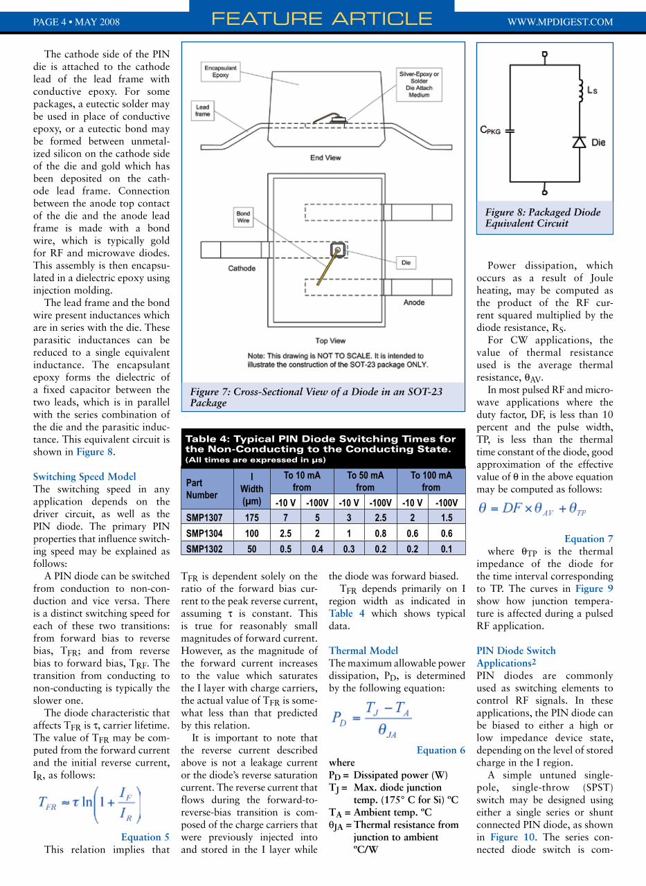
The cathode side of the PIN die is attached to the cathode lead of the lead frame with conductive epoxy. For some packages, a eutectic solder may be used in place of conductive epoxy, or a eutectic bond may be formed between unmetal-ized silicon on the cathode side of the die and gold which has been deposited on the cath-ode lead frame. Connection between the anode top contact of the die and the anode lead frame is made with a bond wire, which is typically gold for RF and microwave diodes. This assembly is then encapsu-lated in a dielectric epoxy using injection molding.
The lead frame and the bond wire present inductances which are in series with the die. These parasitic inductances can be reduced to a single equivalent inductance. The encapsulant epoxy forms the dielectric of a fixed capacitor between the two leads, which is in parallel with the series combination of the die and the parasitic induc-tance. This equivalent circuit is shown in Figure 8.
Switching Speed ModelThe switching speed in any application depends on the driver circuit, as well as the PIN diode. The primary PIN properties that influence switch-ing speed may be explained as follows:
A PIN diode can be switched from conduction to non-con-duction and vice versa. There is a distinct switching speed for each of these two transitions: from forward bias to reverse bias, TFR; and from reverse bias to forward bias, TRF. The transition from conducting to non-conducting is typically the slower one.
The diode characteristic that affects TFR is τ, carrier lifetime. The value of TFR may be com-puted from the forward current and the initial reverse current, IR, as follows:
Equation 5This relation implies that
TFR is dependent solely on the ratio of the forward bias cur-rent to the peak reverse current, assuming τ is constant. This is true for reasonably small magnitudes of forward current. However, as the magnitude of the forward current increases to the value which saturates the I layer with charge carriers, the actual value of TFR is some-what less than that predicted by this relation.
It is important to note that the reverse current described above is not a leakage current or the diode’s reverse saturation current. The reverse current that flows during the forward-to-reverse-bias transition is com-posed of the charge carriers that were previously injected into and stored in the I layer while
the diode was forward biased.TFR depends primarily on I
region width as indicated in Table 4 which shows typical data.
Thermal ModelThe maximum allowable power dissipation, PD, is determined by the following equation:
Equation 6wherePD = Dissipated power (W)TJ = Max. diode junction temp. (175° C for Si) ºCTA = Ambient temp. ºCqJA = Thermal resistance from junction to ambient ºC/W
Power dissipation, which occurs as a result of Joule heating, may be computed as the product of the RF cur-rent squared multiplied by the diode resistance, RS.
For CW applications, the value of thermal resistance used is the average thermal resistance, qAV.
In most pulsed RF and micro-wave applications where the duty factor, DF, is less than 10 percent and the pulse width, TP, is less than the thermal time constant of the diode, good approximation of the effective value of q in the above equation may be computed as follows:
Equation 7where qTP is the thermal
impedance of the diode for the time interval corresponding to TP. The curves in Figure 9 show how junction tempera-ture is affected during a pulsed RF application.
PIN Diode Switch Applications2
PIN diodes are commonly used as switching elements to control RF signals. In these applications, the PIN diode can be biased to either a high or low impedance device state, depending on the level of stored charge in the I region.
A simple untuned single-pole, single-throw (SPST) switch may be designed using either a single series or shunt connected PIN diode, as shown in Figure 10. The series con-nected diode switch is com-
PAGE 4 • MAY 2008 www.MPdiGEst.coMFEATURE ARTICLE
Figure 8: Packaged Diode Equivalent Circuit
Figure 7: Cross-Sectional View of a Diode in an SOT-23 Package
Part Number
I Width(µm)
To 10 mA from
To 50 mA from
To 100 mA from
-10 V -100V -10 V -100V -10 V -100V
SMP1307 175 7 5 3 2.5 2 1.5
SMP1304 100 2.5 2 1 0.8 0.6 0.6
SMP1302 50 0.5 0.4 0.3 0.2 0.2 0.1
Table 4: Typical PIN Diode Switching Times for the Non-Conducting to the Conducting State. (All times are expressed in µs)

monly used when minimum insertion loss is required over a broad frequency range. This design is also easier to physically realize using printed circuit techniques, since no through holes are required in the circuit board to provide a connection to ground.
A single shunt mounted diode will, on the other hand, produce higher isolation values across a wider frequency range and will result in a design capable of han-dling more power since it is easier to heat sink the diode. This configuration does require a very low impedance connection to ground for one end of the diode.
Multithrow switches are used more frequently than single-throw switches. A simple multithrow switch may be designed employing a series PIN diode in each arm adjacent to the common port, as shown in Figure 11.
Improved performance is obtained by using “compound switches,” which are combinations of series and shunt con-nected PIN diodes, in each arm of the switch. For narrow-band applications, quarter-wave spaced multiple diodes may also be used in various switch designs to obtain improved operation.
Figures 10a and 11 show two basic types of PIN diode series switches, (SPST and SPDT), commonly used in broad-band designs. In both cases, the diode is in a “pass power” condition when it is forward biased and presents a low forward resistance between the RF gen-erator and load. For the “stop power” condition, the diode is at zero or reverse bias so that it presents a high impedance between the source and load. In series connected switches, the maximum iso-lation obtainable depends primarily on the capacitance of the PIN diode, while the insertion loss and power dissipation are functions of the diode resistance. The principal operating parameters of a series switch may be obtained using the following equations:
Insertion Loss (Series Switch)
Equation 8
This equation applies for an SPST switch and is graphically presented in Figure 12 for a 50 Ω impedance design. For multithrow switches, the insertion loss is slightly higher due to any mis-match caused by the capacitance of the PIN diodes in the “off” arms. This addi-tional insertion loss can be determined from Figure 12, after first computing the
total shunt capacitance of all “off” arms of the multithrow switch.
Isolation (Series Switch)
Equation 9
This equation applies for an SPST diode switch. Add 6 dB for an SPNT switch to account for the 50 percent voltage reduction across the “off” diode, due to the termination of the generator in its characteristic impedance. Figure 12 graphically presents isolation as a function of capacitance for simple series switches. These curves are plotted for circuits terminated in 50 Ω loads.
RF Power Dissipation (Series Switch in Forward Bias)
Equation 10
For Z0 >> RS, this becomes
Equation 11
where the maximum available power is given by
Equation 12
It should be noted that Equations 10 and 11 apply only for perfectly matched switches. For SWR (σ) values other than unity, multiply these equations by
to obtain the maximum required diode power dissipation rating.
Peak RF Current (Series Switch)
Equation 13
In the case of a 50 Ω system this becomes
PAGE 5 • MAY 2008 www.MPdiGEst.coMFEATURE ARTICLE
Figure 10: Simple PIN Diode SPST Switches
Figure 9: Diode Power Dissipation and Junction Temperature versus Time for a Pulsed RF Signal
Figure 11: Simple PIN Diode SPDT Switch

Equation 14
Peak RF Voltage (Series Switch)
Equation 15
For a 50 Ω system this becomes
Equation 16
Equation 17
Equation 18
Shunt Connected SwitchFigures 13 and 14 show two typical shunt connected PIN diode switches. These shunt diode switches offer high isola-tion for many applications, and since the diode may be heat sunk at one electrode it is capa-ble of handling more RF power than a diode in a series type switch. In shunt switch designs, the isolation and power dissipa-tion are functions of the diode’s forward resistance, whereas the insertion loss is primarily dependent on the capacitance of the PIN diode. The princi-pal equations describing the
operating parameters of shunt switches are given by:
Insertion Loss (Shunt Switch)
Equation 19This equation applies for
both SPST and SPNT shunt switches and is graphically pre-sented in Figure 15 for a 50 Ω load impedance design.
Isolation (Shunt Switch)
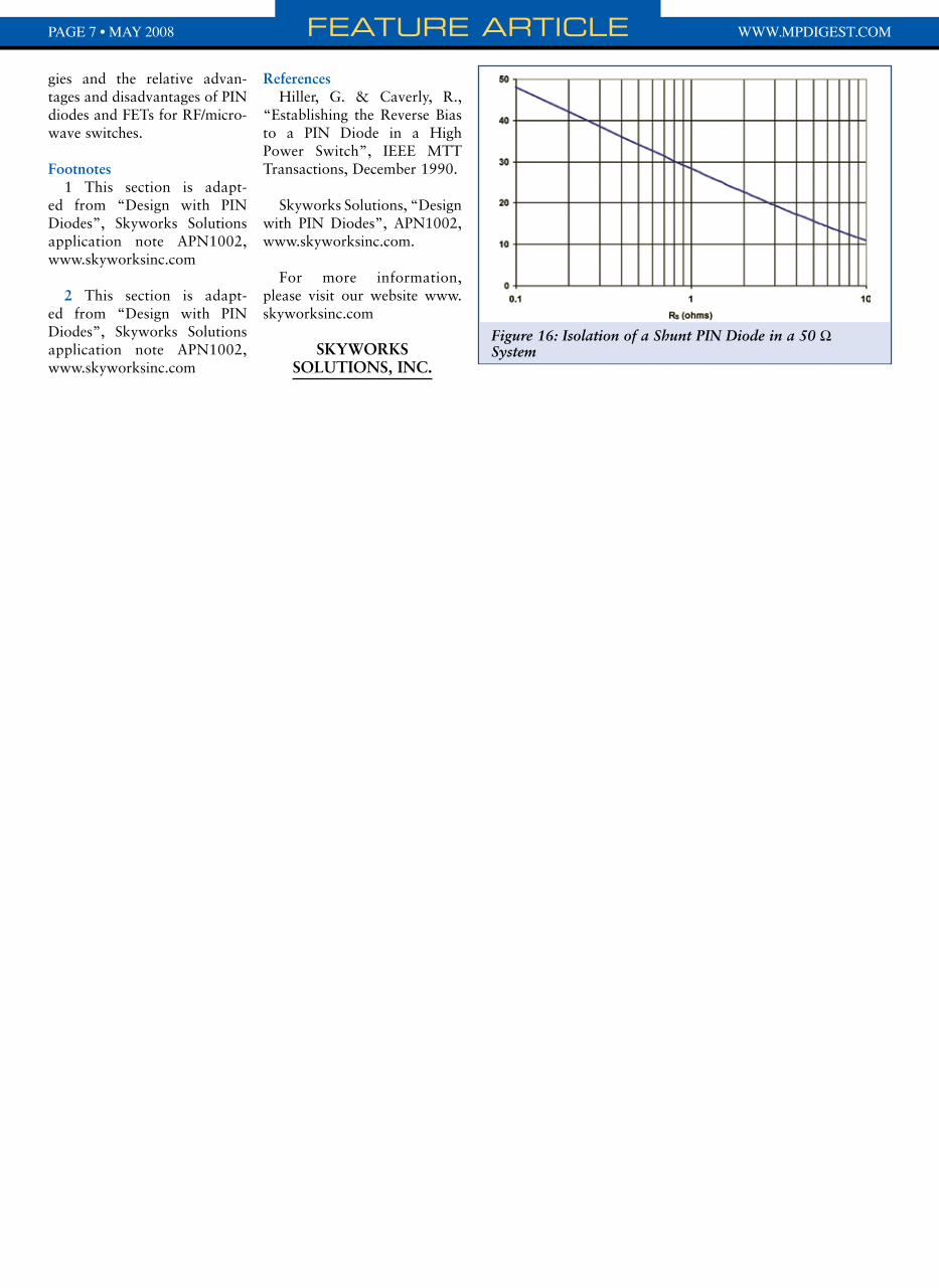
Equation 20This equation, which is illus-
trated in Figure 16, applies for an SPST shunt switch. Add 6 dB to these values to obtain the
correct isolation for a multi-throw switch.
Peak RF Voltage (Shunt Switch)
Equation 21In the case of a 50 Ω system
this becomes
Equation 22
ConclusionIn part 2 of this article, we will describe compound tuned PIN diode switches, RF/microwave field effect transistor (FET) topology and theory of opera-tion, some FET switch topolo-
PAGE 6 • MAY 2008 www.MPdiGEst.coMFEATURE ARTICLE
Figure 14: SPST Switch with Shunt Connected PIN Diode
Figure 13: SPDT Switch with Shunt Connected PIN DiodesFigure 12: Isolation for a Series Diode in a 50 Ω System for 0.2 ≤ CT ≤ 5 pF
Figure 15: Insertion Loss of a Shunt PIN Diode in a 50 Ω System for 0.2 ≤ CT ≤ 5 pF
PAGE 7 • MAY 2008 www.MPdiGEst.coMFEATURE ARTICLE
Figure 16: Isolation of a Shunt PIN Diode in a 50 Ω System
gies and the relative advan-tages and disadvantages of PIN diodes and FETs for RF/micro-wave switches.
Footnotes1 This section is adapt-
ed from “Design with PIN Diodes”, Skyworks Solutions application note APN1002, www.skyworksinc.com
2 This section is adapt-ed from “Design with PIN Diodes”, Skyworks Solutions application note APN1002, www.skyworksinc.com
ReferencesHiller, G. & Caverly, R.,
“Establishing the Reverse Bias to a PIN Diode in a High Power Switch”, IEEE MTT Transactions, December 1990.
Skyworks Solutions, “Design with PIN Diodes”, APN1002, www.skyworksinc.com.
For more information, please visit our website www.skyworksinc.com
SkyWORkS SOLuTIONS, INC.