page 01- 1 architecture introduction objective: use your architectural knowledge to maximize...
TRANSCRIPT

Page 01- 1
Architecture Introduction
Objective:• Use your architectural knowledge to maximize concurrency for execution speed• Distinguish among various operand types and sizes• Convergently round numbers • Use the Status Register to:
- Scale data- Detect data growth- Adjust global interrupt mask priority
• Detect out of range numbers• Utilize no-overhead looping

Page 01- 2
Intentional blank page
Page 01- 3
Table of Contents
4...Basic DSP Operations5..Typical Block Diagram of a System6…Features 9…Program Buses10..Fetch Set and Execution Set11..Data Buses13..Core Block Diagram14..Word Operand17..Fractional Examples - Word18..Long Word Operand21..Data Register Operand 23..Data Register Operand Examples24..Fractional vs. Integer Multiplication25...Data ALU Architecture26..Data ALU Programming Model27..Analog Saturation Arithmetic
28..Digital Saturation Arithmetic29..Convergent Rounding 32..AGU Programming Model33..Program Sequencer Unit34..Status Register35..Exception and Mode Register36..Loop Counter and Start Address Registers37..Pipeline38..Fetch Set and Execution Set39..Stack Support43..Fast Return from Subroutine 44..Do Loop Operation45..Loop Examples 48..Iteration and Termination of Loops50..Looping Restrictions

Page 01- 4
Basic DSP Operations
x(t)
"FIR" Filter
Finite ImpulseResponse
c(k) x(n-k)N-1
k = 0 D/AA/D y(t)
Low PassAntialiasing Filter
Sampler andAnalog toDigitalConverter
DigitalSignalProcessing Operation
Digitalto AnalogConverter
ReconstructionLow PassFilter
Digital Filter
Analog Out
Analog In
x(n) y(n)
Page 01- 5
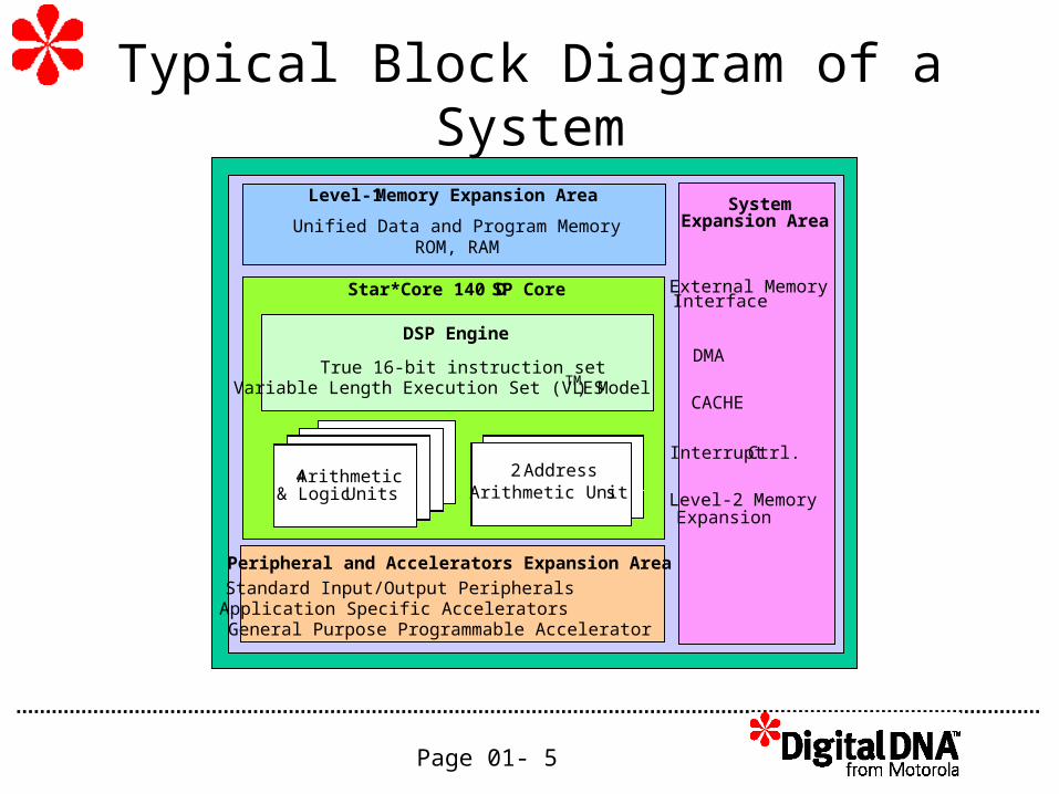
Typical Block Diagram of a System
Level-1 Memory Expansion Area
Unified Data and Program MemoryROM, RAM
DSP Engine
True 16-bit instruction set
Star*Core 140 DSP Core
System
External Memory
DMA
CACHE
Peripheral and Accelerators Expansion Area
Standard Input/Output PeripheralsApplication Specific AcceleratorsGeneral Purpose Programmable Accelerator
4 Arithmetic
Expansion Area
Interface
Interrupt Ctrl.
Variable Length Execution Set (VLESTM) Model
Level-2 Memory Expansion
2 AddressArithmetic Units& Logic Units
Page 01- 6
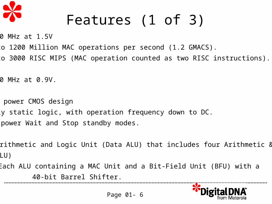
Features (1 of 3)Up to 300 MHz at 1.5V
•Up to 1200 Million MAC operations per second (1.2 GMACS).
•Up to 3000 RISC MIPS (MAC operation counted as two RISC instructions).
Up to 120 MHz at 0.9V.
Very low power CMOS design
•Fully static logic, with operation frequency down to DC.
•Low power Wait and Stop standby modes.
A Data Arithmetic and Logic Unit (Data ALU) that includes four Arithmetic & Logic
Units (ALU)
•Each ALU containing a MAC Unit and a Bit-Field Unit (BFU) with a
40-bit Barrel Shifter.
Page 01- 7
Oneinstruction
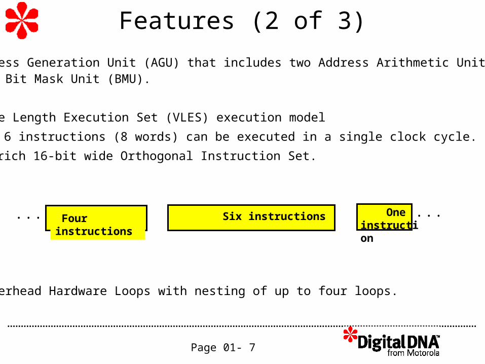
An Address Generation Unit (AGU) that includes two Address Arithmetic Units (AAU) and one Bit Mask Unit (BMU).
Variable Length Execution Set (VLES) execution model
•Up to 6 instructions (8 words) can be executed in a single clock cycle.
•Very rich 16-bit wide Orthogonal Instruction Set.
Zero overhead Hardware Loops with nesting of up to four loops.
Features (2 of 3)
Four instructions Six instructions • • •• • •
Page 01- 8
Features (3 of 3)
Position Independent Code (PIC) PC-Relative change-of-flow Instructions.
Enhanced On-Chip Emulation (EOnCETM) module with Real-Time debug capabilities.
Unified Data and Program Memory space
•32-bit address space for both program and data memory
•Byte addressability to data memory
Page 01- 9
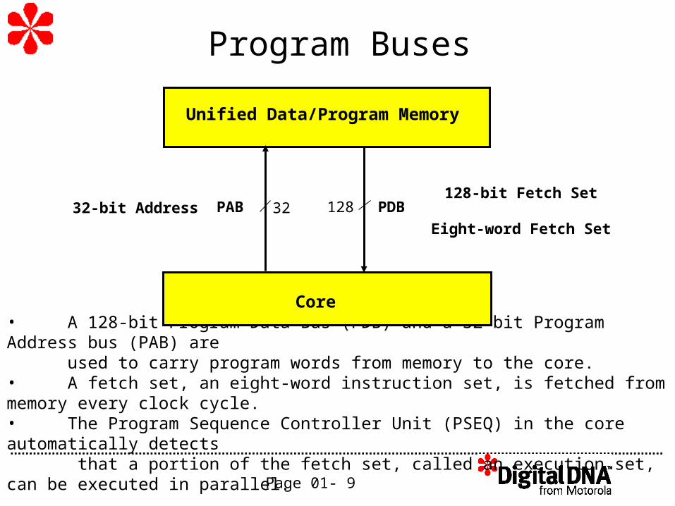
Program Buses
• A 128-bit Program Data Bus (PDB) and a 32-bit Program Address bus (PAB) are used to carry program words from memory to the core.• A fetch set, an eight-word instruction set, is fetched from memory every clock cycle.
• The Program Sequence Controller Unit (PSEQ) in the core automatically detects that a portion of the fetch set, called an execution set, can be executed in parallel.
32 128PAB PDB
Unified Data/Program Memory
Core
128-bit Fetch Set
Eight-word Fetch Set
32-bit Address
Page 01- 10
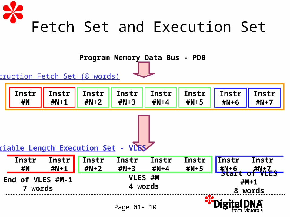
Fetch Set and Execution Set
Instr#N
Instr#N+1
Instr#N+2
Instr#N+3
Instr#N+4
Instr#N+5
Instr#N+6
Instr#N+7
Instr#N
Instr#N+1
Instr#N+2
Instr#N+3
Instr#N+4
Instr#N+5
Instr#N+6
Instr#N+7
Variable Length Execution Set - VLES
Instruction Fetch Set (8 words)
Program Memory Data Bus - PDB
End of VLES #M-17 words
VLES #M4 words
Start of VLES #M+18 words
Page 01- 11
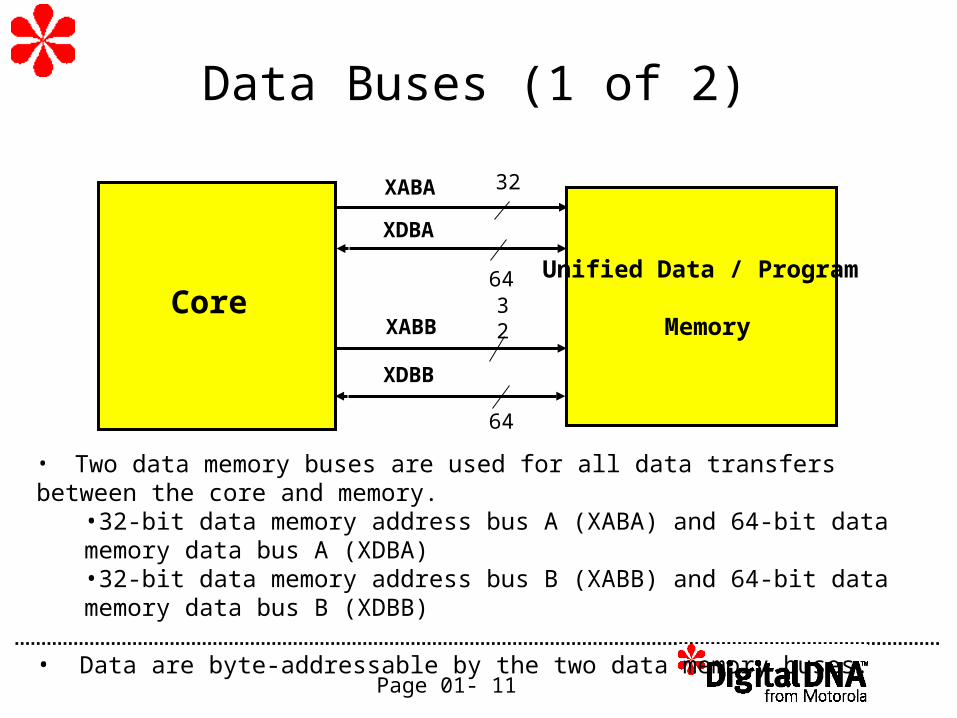
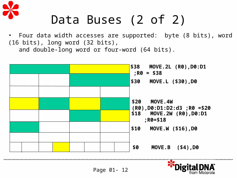
Data Buses (1 of 2)
• Two data memory buses are used for all data transfers between the core and memory.•32-bit data memory address bus A (XABA) and 64-bit data memory data bus A (XDBA) •32-bit data memory address bus B (XABB) and 64-bit data memory data bus B (XDBB)
• Data are byte-addressable by the two data memory buses.
Unified Data / Program
Memory
XABA
XDBA
XABB
XDBB
32
64
64
32
Core
Page 01- 12
Data Buses (2 of 2)• Four data width accesses are supported: byte (8 bits), word (16 bits), long word (32 bits), and double-long word or four-word (64 bits).
$0 MOVE.B ($4),D0
$10 MOVE.W ($16),D0
$18 MOVE.2W (R0),D0:D1 ;R0=$18
$20 MOVE.4W (R0),D0:D1:D2:d3 ;R0 =$20
$30 MOVE.L ($30),D0
$38 MOVE.2L (R0),D0:D1 ;R0 = $38
Page 01- 13
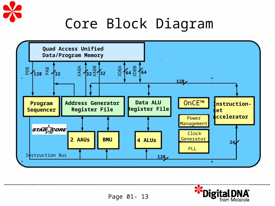
Core Block Diagram
Instruction Bus
ProgramSequencer
2 AAUs 4 ALUs
Address GeneratorRegister File
Data ALURegister File
Instruction-setAccelerator
OnCE™
Quad Access UnifiedData/Program Memory
140
128
6464323232128
128
BMU 24
PowerManagement
ClockGenerator
PLL
PA
B
PD
B
XA
BA
XD
BB
XD
BA
XA
BB

Page 01- 14
Word Operand: 16-bit Signed Integer
-215 214 213
• • •
14 1315
21 20
1 0
Most Positive Integer215 - 1 = $7FFF
Most Negative Integer- 215 = $8000
Storage LocationsMemory and Data Registers
•BinaryPoint
SIGN

Page 01- 15
Word Operand: 16-bit Unsigned Integer
215 214 213
• • •
14 1315
21 20
1 0
Largest Unsigned Integer216 - 1 = $FFFF
Smallest Unsigned Integer0 = $0000
Storage LocationsMemory and Data Registers
•
Page 01- 16
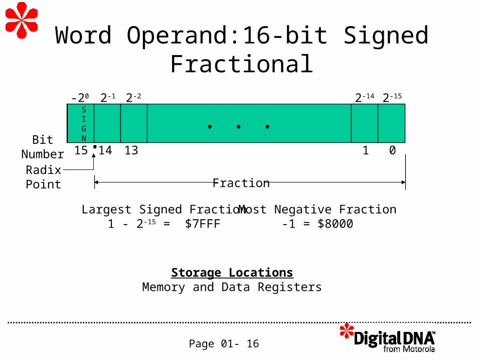
Word Operand:16-bit Signed Fractional
-20 2-1 2-2
• • •
14 1315
2-14 2-15
1 0Bit
Number
Largest Signed Fraction1 - 2-15 = $7FFF
Most Negative Fraction-1 = $8000
Storage LocationsMemory and Data Registers
•
RadixPoint Fraction
SIGN

Page 01- 17
Fractional Examples - Word
Decimal Fraction 16-Bit Binary Value
Hexadecimal Representation
0.750 0.1100000 00000000 $6000 0.500 0.1000000 00000000 $4000 0.250 0.0100000 00000000 $2000 0.125 0.0010000 00000000 $1000-0.125 1.1110000 00000000 $F000-0.750 1.0100000 00000000 $A000

Page 01- 18
Long Word Operand: 32-bit Signed Integer
-231 230 229
• • •
30 2931
21 20
1 0
Most Positive Integer 231-1 = $7FFFFFFF
Most Negative Integer - 231 = $80000000
Storage LocationsMemory and Data Registers
•
SIGN

Page 01- 19
Long Word Operand: 32-bit Unsigned Integer
231 230 229
• • •
30 2931
21 20
1 0
Largest Unsigned Integer232 -1 = $FFFFFFFF
Smallest Unsigned Integer0 = $00000000
Storage LocationsMemory and Data Registers
•
Page 01- 20
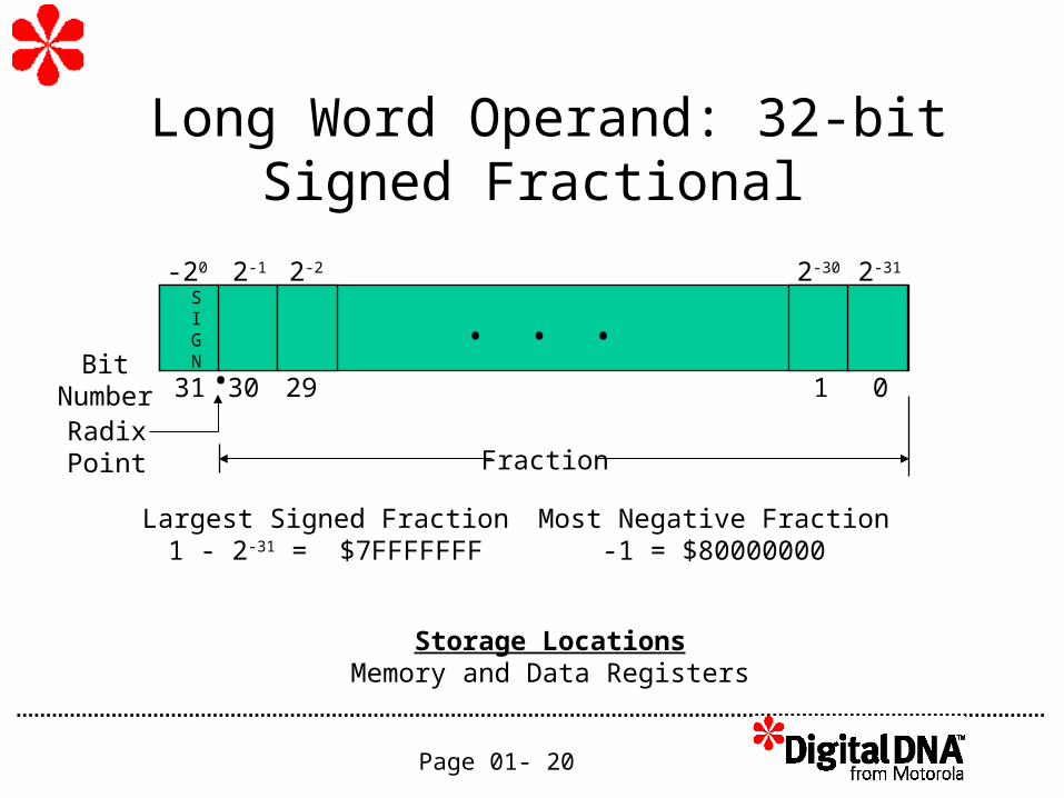
Long Word Operand: 32-bit Signed Fractional
-20 2-1 2-2
• • •
30 2931
2-30 2-31
1 0Bit
Number
Largest Signed Fraction1 - 2-31 = $7FFFFFFF
Most Negative Fraction-1 = $80000000
Storage LocationsMemory and Data Registers
•
RadixPoint Fraction
SIGN
Page 01- 21
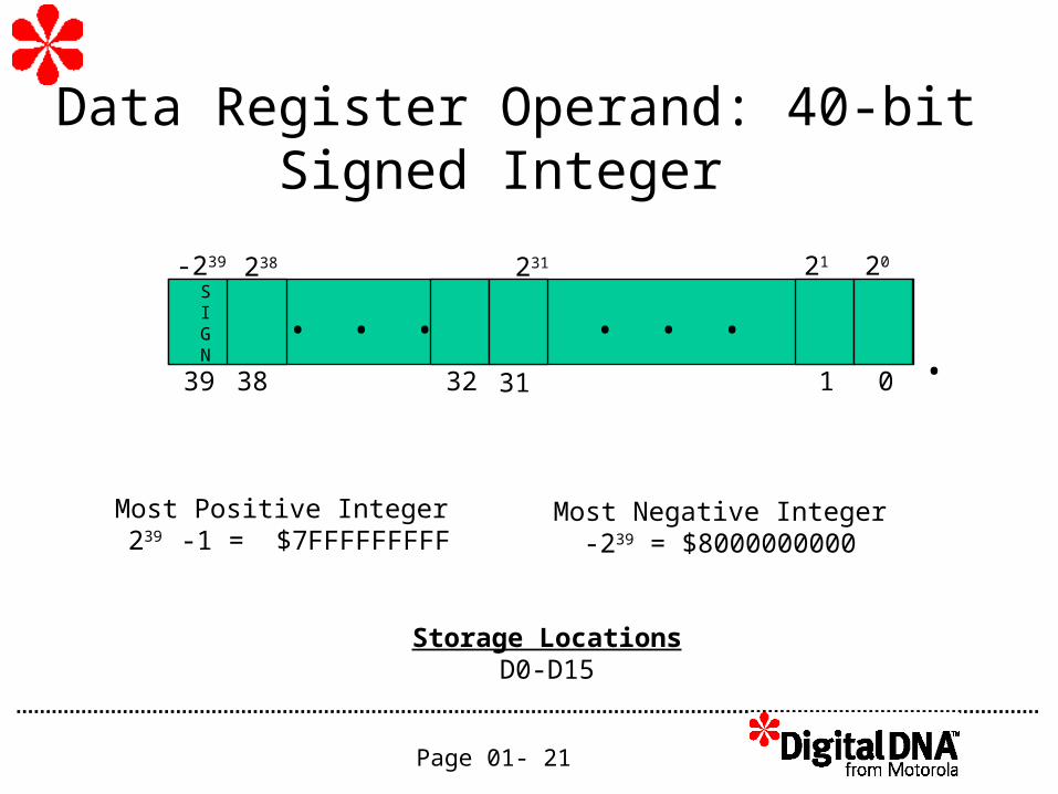
Data Register Operand: 40-bit Signed Integer
-239
• • •
38 3239
21 20
1 0
Most Positive Integer 239 -1 = $7FFFFFFFFF
Most Negative Integer-239 = $8000000000
Storage LocationsD0-D15
•
SIGN
• • •
31
231238
Page 01- 22
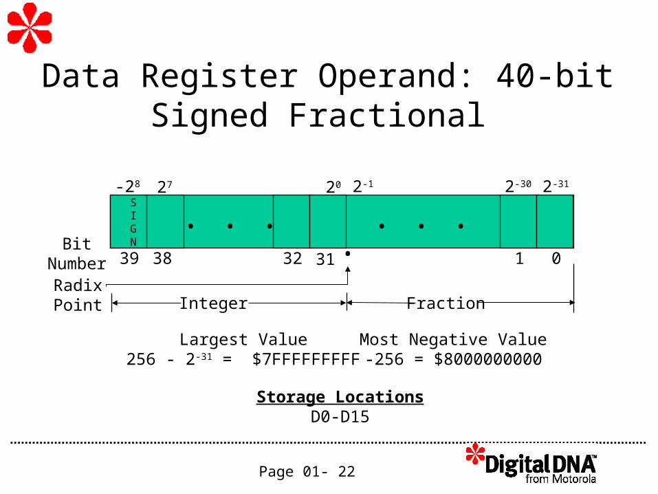
Data Register Operand: 40-bit Signed Fractional
-28 2-1
• • •
38 3239
2-30 2-31
1 0Bit
Number
Largest Value256 - 2-31 = $7FFFFFFFFF
Most Negative Value-256 = $8000000000
Storage LocationsD0-D15
•
RadixPoint Fraction
SIGN
• • •
31
2027
Integer
Page 01- 23
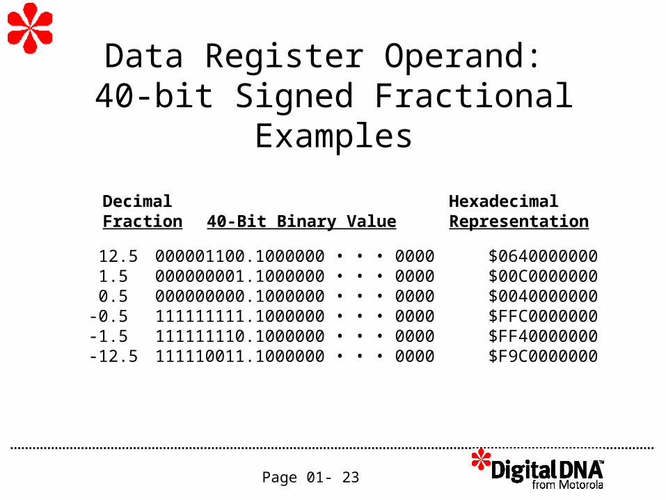
Data Register Operand: 40-bit Signed Fractional Examples
Decimal Fraction 40-Bit Binary Value
Hexadecimal Representation
12.5 000001100.1000000 • • • 0000 $0640000000 1.5 000000001.1000000 • • • 0000 $00C0000000 0.5 000000000.1000000 • • • 0000 $0040000000-0.5 111111111.1000000 • • • 0000 $FFC0000000-1.5 111111110.1000000 • • • 0000 $FF40000000-12.5 111110011.1000000 • • • 0000 $F9C0000000

Page 01- 24
Fractional vs. Integer Multiplication
S S
S
2N Bits
S S
0
2N—1 Product
2N Bits
Integer Fractional
Sign Extension Zero Fill
Signed Multiplier Signed Multiplier
S MSP LSP S MSP LSP
X
... ...
.. ..
. .
X
2N—1 Product

Page 01- 25
Data ALU Architecture
Memory data bus 1 (XDBA)
Memory data bus 2 (XDBB)
64 64
40 4040 40
64 64
Data Register File
ALU ALU ALUALU
Shifter/Limiter
40 40
40 4040 40

Page 01- 26
L0 D0.e D0.h D0.lL1 D1.e D1.h D1.lL2 D2.e D2.h D2.lL3 D3.e D3.h D3.lL4 D4.e D4.h D4.lL5 D5.e D5.h D5.lL6 D6.e D6.h D6.lL7 D7.e D7.h D7.lL8 D8.e D8.h D8.lL9 D9.e D9.h D9.lL10 D10.e D10.h D10.lL11 D11.e D11.h D11.lL12 D12.e D12.h D12.lL13 D13.e D13.h D13.lL14 D14.e D14.h D14.lL15 D15.e D15.h D15.l
Data ALU Programming Model
39 32 16 15 0
Page 01- 27
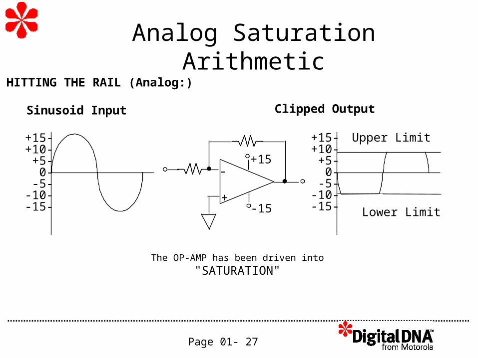
Analog Saturation ArithmeticHITTING THE RAIL (Analog:)
+15
-15+
-
Clipped Output
The OP-AMP has been driven into
"SATURATION"
Sinusoid Input
Lower Limit
Upper Limit+15-+10-+5-
0--5-
-10--15-
+15-+10-+5-
0--5-
-10--15-

Page 01- 28
1 0...0 0 0 . . . 0 0
150 1 1 ... 1 11 0 0 ... 0 0
1 0 0 ... 0 0
Digital Saturation Arithmetic
Without Limiting
Dx = +1.0
= -1.0
|Error| = 2.0
0...0 0 0 . . . 0 015 01632
Dx.h
31
= +0.9999999
|Error| = 0.0000001
With Limiting
15 0
HITTING THE RAIL (Digital:)
Dx.lDx.e
391 0 0 ... 0 0 Dx = +1.0
15 01632
Dx.h
31
0
Dx.lDx.e
39
Lx1
Lx
MOVE.F D0,(R0) MOVES.F D0,(R0)

Page 01- 29
Convergent Rounding (1 of 3)
The Problem:
Round Up to 10
??? Which Way ???
Round Down to 0
Rounding Five toEither Direction Creates a Bias
Rounding:
The Solution: Convergent Rounding or Round to Nearest Even.
10 9 8 7 6 5 4 3 2 1 0
Oh! Nooooooooo

Page 01- 30
Convergent Rounding (2 of 3)
Case II: If D0.l > $8000 (1/2), then round up (add 1 to D0.h)
X...XD0.e
XX...XX0100 1110X..…XXD0.h D0.l
1
3932 31 16 15 0
Before Rounding: After Rounding:
Case I: If D0.l < $8000 (1/2), then round down (add nothing)
X...XD0.e
XX...XX0100 01XX..…XXXD0.h D0.l
0
39 32 31 16 15 0
Before Rounding:
X...XD0.e
XX...XX0100 0000.....0000D0.h D0.l
39 32 31 16 15 0
After Rounding:
X...XD0.e
XX...XX0101 0000.....0000D0.h D0.l
3932 31 16 15 0
Convergent Rounding Examples:

Page 01- 31
Convergent Rounding (3 of 3)
Case IV: If D0.l = $8000 (1/2), and the least significant bit of D0.h = 1, then round up (add one)
X...XD0.e
XX...XX0101 1000.....0000D0.h D0.l
1
3932 31 16 15 0
Before Rounding: After Rounding:
Case III: If D0.l = $8000 (1/2), and the least significant bit of D0.h = 0, then round down (add nothing)
X...XD0.e
XX...XX01001000..…0000D0.h D0.l
0
39 32 31 16 15 0
Before Rounding:
X...XD0.e
XX...XX0100 0000.....0000D0.h D0.l
39 32 31 16 15 0
After Rounding:
X...XD0.e
XX...XX0110 0000.....0000D0.h D0.l
3932 31 16 15 0
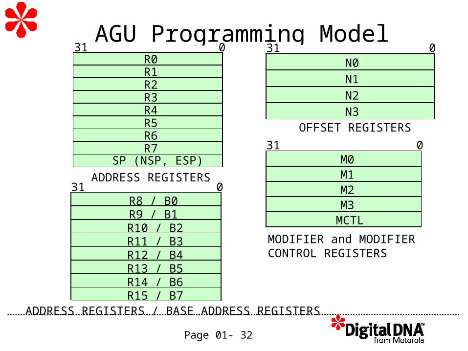
Page 01- 32
AGU Programming Model031
ADDRESS REGISTERS
R0
R2R3
R1
R4R5R6R7
SP (NSP, ESP)
MODIFIER and MODIFIER CONTROL REGISTERS
031M0M1M2
MCTLM3
ADDRESS REGISTERS / BASE ADDRESS REGISTERS
031R8 / B0
R10 / B2R11 / B3
R9 / B1
R12 / B4R13 / B5R14 / B6R15 / B7
N0
N1
031
N2N3
OFFSET REGISTERS
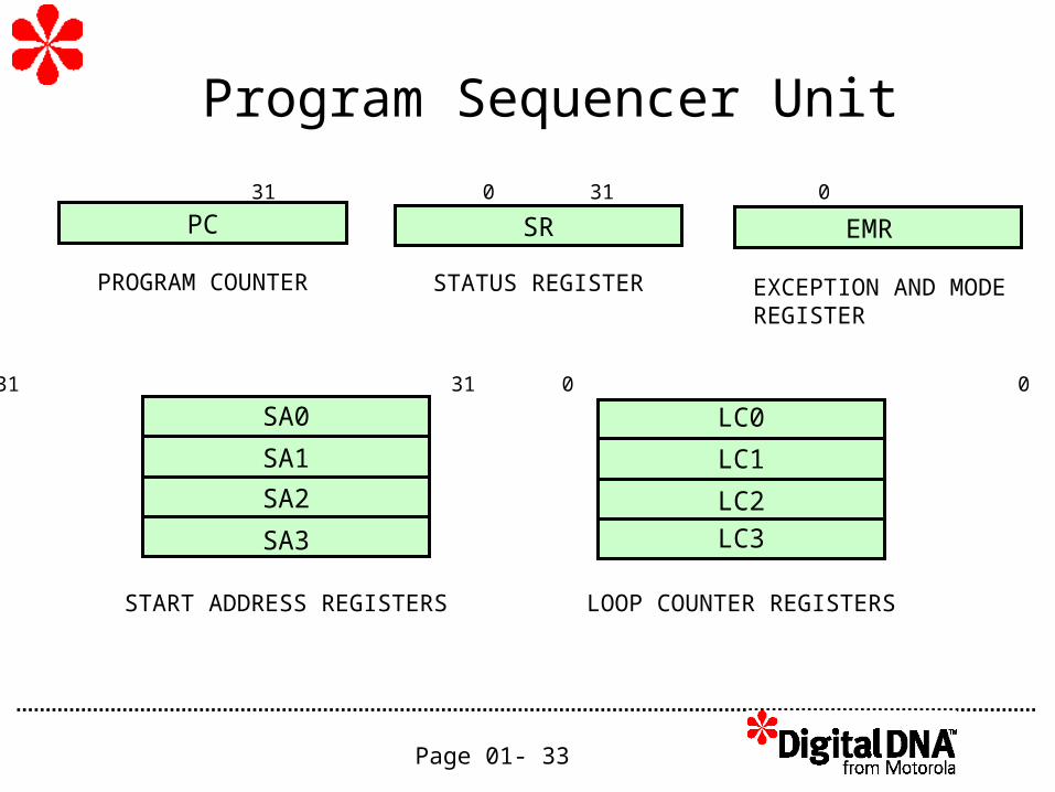
Page 01- 33
Program Sequencer Unit
PC
LC3
LC2
LC1
LC0
SA3
SA2
SA1
SA0
EMRSR
PROGRAM COUNTER
LOOP COUNTER REGISTERSSTART ADDRESS REGISTERS
STATUS REGISTER EXCEPTION AND MODE REGISTER
31 0
31 0 31 0
31 0 31 0

Page 01- 34
Status Register
31 30-27 26-24 23-21 20 19 18 17-12 11-8 7 6 5 4 3 2 1 0SLF LF[3:0] Rsvd I[2:0] OVE DI EXP Rsvd VF[3:0] Rsvd S S1 S0 RM AS T C
SLF - Short Loop Flag LF[3:0] - Loop Flags I[2:0] - Interrupt Mask OVE - Overflow Exception Enable DI - Disable Interrupts EXP - Exception Mode bit VF[3:0] - Viterbi Flags S - Scaling Bit S1, S0 - Scaling Mode Bits RM - Rounding Mode AS -Arithmetic Saturation Mode T - True Bit C - Carry Bit*Rsvd - Reserved (derivative dependant)
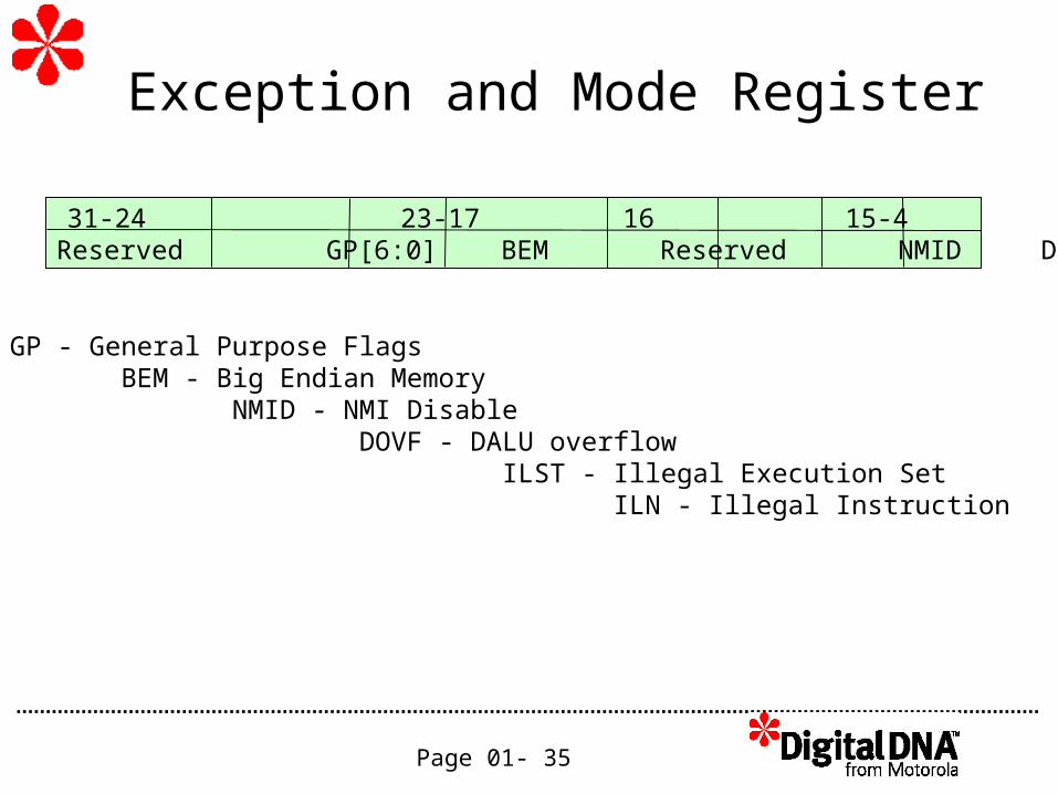
Page 01- 35
Exception and Mode Register
31-24 23-17 16 15-4 3 2 1 0Reserved GP[6:0] BEM Reserved NMID DOVF ILST ILN
GP - General Purpose Flags BEM - Big Endian Memory NMID - NMI Disable DOVF - DALU overflow ILST - Illegal Execution Set ILN - Illegal Instruction
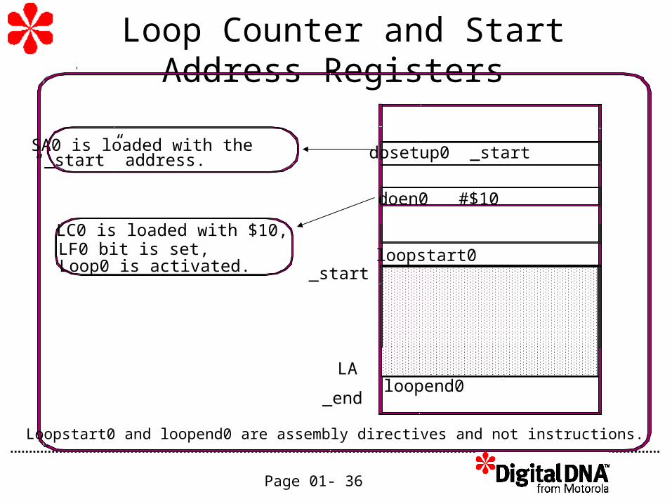
Page 01- 36
Loop Counter and Start Address Registers
dosetup0 _start
doen0 #$10
_end
SA0 is loaded with the“_start” address.
LC0 is loaded with $10,LF0 bit is set,Loop0 is activated.
loopstart0
loopend0
_start
Loopstart0 and loopend0 are assembly directives and not instructions.
LA
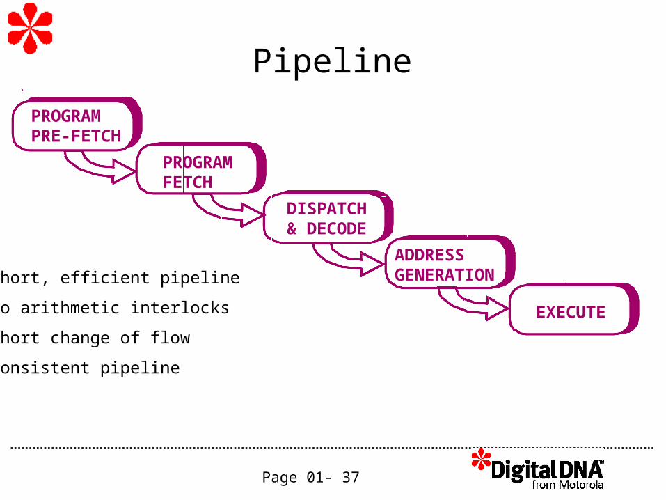
Page 01- 37
Pipeline
PROGRAMPRE-FETCH
PROGRAMFETCH
DISPATCH& DECODE
ADDRESSGENERATION
EXECUTE
- Short, efficient pipeline
- No arithmetic interlocks
- Short change of flow
- Consistent pipeline

Page 01- 38
Fetch Set and Execution Set
Instr#N
Instr#N+1
Instr#N+2
Instr#N+3
Instr#N+4
Instr#N+5
Instr#N+6
Instr#N+7
Instr#N
Instr#N+1
Instr#N+2
Instr#N+3
Instr#N+4
Instr#N+5
Instr#N+6
Instr#N+7
Variable Length Execution Set - VLES
Instruction Fetch Set (8 words)
Program Memory Data Bus - PDB
End of VLES #M-17 words
VLES #M4 words
Start of VLES #M+18 words

Page 01- 39
Stack Support (1 of 4)
Normal mode stack:
Exception mode stack:
Increasingaddresses
ESP
Shadow ESPShadow ESP
Last stacked value - 8 bytes
Last stacked value - 8 bytes
Increasingaddresses
NSP
ShadowShadow NSPNSP1
Valid bit
1Valid bit

Page 01- 40
Stack Support (2 of 4)
Exception mode stack:
Increasingaddresses
SP
DeIncreasingaddresses
SP
PUSH De
De (SP)SP + 8 SP
Do
PUSH Do
Do (SP+4)SP + 8 SP
Page 01- 41
Stack Support (3 of 4)
Exception mode stack:
Increasingaddresses
SP
DeIncreasingaddresses SP
POP De
(SP - 8) De SP-8 SP
Do
POP Do
(SP - 4) DoSP-8 SP
Page 01- 42
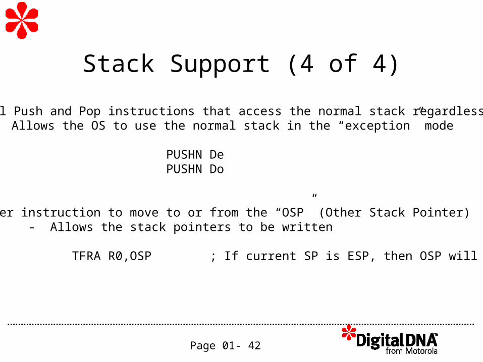
Stack Support (4 of 4)
• Special Push and Pop instructions that access the normal stack regardless of mode- Allows the OS to use the normal stack in the “exception” mode
PUSHN De PUSHN Do
• Transfer instruction to move to or from the “OSP” (Other Stack Pointer) - Allows the stack pointers to be written
TFRA R0,OSP ; If current SP is ESP, then OSP will be NSP
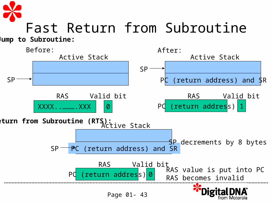
Page 01- 43
Fast Return from Subroutine
PC (return address) and SR
SP
PC (return address)
RAS
Active Stack
SP
XXXX..……….XXX
RAS
Active Stack
Jump to Subroutine:
Before: After:
Return from Subroutine (RTS):
PC (return address) and SRSP
PC (return address)
RAS
Active Stack
SP decrements by 8 bytes
RAS value is put into PCRAS becomes invalid
0 1
0
Valid bitValid bit
Valid bit

Page 01- 44
Do Loop Operation
dosetup0 _start
doen0 R1
_end
SA0 is loaded with the
if LC[active]<=0
jump to SA[active], if LC[active]>1
decrement LC[active].
- Optional -
“_start” address.
skipls _endjump to _end
LC0 is loaded with R1,LF0 bit is set,Loop0 is activated.
if LC[active]<=1clear LF[active] bit
loopstart0
loopend0
Assembly signal
_start
(not an instruction)
and clear LF[active]

Page 01- 45
Long Loop:dosetup0 _ start0doen0 #$10move.w (r3)+,d1skipls _end0loopstart0
SA _start0mac d0,d1,d2 move.w (r0)+,d0add d5,d6,d4 move.w (r1)+,d5sub d3,d2,d4 inc d5 LPMARKBmac d0,d1,d6 move.w (r0)+,d7
LA sub d5,d4,d4 inc d7loopend0
_end0
Loop Examples (1 of 3)
Page 01- 46
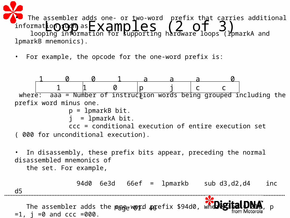
• The assembler adds one- or two-word prefix that carries additional information such as looping information for supporting hardware loops (lpmarkA and lpmarkB mnemonics).
• For example, the opcode for the one-word prefix is:
where: aaa = Number of instruction words being grouped including the prefix word minus one. p = lpmarkB bit. j = lpmarkA bit. ccc = conditional execution of entire execution set ( 000 for unconditional execution).
• In disassembly, these prefix bits appear, preceding the normal disassembled mnemonics of the set. For example,
94d0 6e3d 66ef = lpmarkb sub d3,d2,d4 inc d5
The assembler adds the one-word prefix $94d0, where aaa = 010, p =1, j =0 and ccc =000.
Loop Examples (2 of 3)
1 0 0 1 a a a 0 1 1 0 p j c c c

Page 01- 47
Loop Examples (3 of 3)Short Loop, two execution sets:
doensh0 #$10...loopstart0
SA mac d0,d1,d2 move.w (r0)+,d0 LPMARKBLA add d5,d6,d4 move.w (r1)+,d5
loopend0
Short Loop, one execution set:
doensh0 #$10...loopstart0
SA, LA mac d0,d1,d2 move.w (r0)+,d0 LPMARKA
loopend0
Page 01- 48
CONT LBL
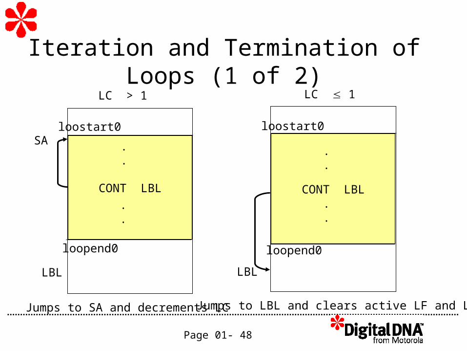
Iteration and Termination of Loops (1 of 2)
LBL LBL
LC > 1 LC 1
SA
Jumps to SA and decrements LC Jumps to LBL and clears active LF and LC.
.
.
.
.
CONT LBL
.
.
.
.
loostart0
loopend0
loostart0
loopend0

Page 01- 49
Iteration and Termination of Loops (2 of 2)
LBL
Jumps to LBL and clears the active LF.
BREAK LBL
loopstart0
loopend0

Page 01- 50
Looping Restrictions (1 of 4)
Loop nesting:
• Nested loops can’t end in the same last address.• Loops must be nested in a specific order: a loop can be nested only inside a loop
with a smaller number.
Loop 0
Loop2
Loop3

Page 01- 51
Looping Restrictions (2 of 4)Minimum distance between looping instructions
• At least one execution set should be between the DOENn/DOENSHn instruction
and the SKIPLS instruction.
doen0 #$10move.w (r3)+,d1skipls _end0
• Between the DOENn/SH instruction and the execution set with the prefix bit (Lpmark),
there should be at least 2 execution sets when writing LCn from a D register and
1 execution set when writing LCn from an R register or immediate value.
doensh0 #$10
move.w (r3)+,d5Loopstart0mac d0,d1,d2 move.w (r0)+,d0 LPMARKB
Page 01- 52
Looping Restrictions (3 of 4)
Change of flow and looping
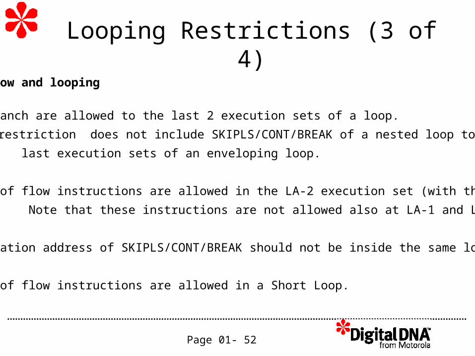
• No jump/branch are allowed to the last 2 execution sets of a loop.
This restriction does not include SKIPLS/CONT/BREAK of a nested loop to the
last execution sets of an enveloping loop.
• No change of flow instructions are allowed in the LA-2 execution set (with the lpmarkb).
Note that these instructions are not allowed also at LA-1 and LA.
• The destination address of SKIPLS/CONT/BREAK should not be inside the same loop.
• No change of flow instructions are allowed in a Short Loop.

Page 01- 53
Looping Restrictions (4 of 4)
Instructions at the end of loops
All restrictions on delay slots which appear in Appendix A are relevant to the last
2 execution sets of each loop.
General looping restrictions
It is not recommended to clear a Loop Flag of a valid loop (or the SLF) by explicit SR
updates, i.e., by instructions that are not loop instructions. It could generate conflicts
in the loop support machine