pad damage overview - its tutorial 2007
TRANSCRIPT

Ken Karklin Touchdown TechnologiesJerry Broz, Ph. D. – SWTW General ChairBill Mann - SWTW Chair Emeritus& SWTW Program Committee
Bond Pad Damage TutorialBond Pad Damage Tutorial
Probe Pad DamageProbe Pad Damage• Damage from Wafer Sort• The Problem and Analysis• Initial Pad Damage Control• Low k Dielectrics and Copper Metalization• Controlling Damage with Probe Card
Technologies• Using the Prober to Control the Probing
Process

IntroductionIntroduction• Probe card technologies have become advanced; BUT,
the basics of wafer sort really have not changed.
• ALL probe technologies have a contact area substantially harder than the pads or solder balls of the device.
• “Contact and slide” is CRITICAL to break surface oxide(s), but results in localized plastic deformation, i.e. a probe mark.
• Volume of material displaced and/or transferred is a complex function of dynamic contact mechanics, metallic interactions, frictional effects, and other tribological properties.

Bond Pad Damage OverviewBond Pad Damage OverviewWhat is bond pad damage?
How do we define it?
How do we measure it?
Roadmap gap assessment and industry trends
Where can I read more on bond pad damage?

Bond Pad DamageBond Pad Damage• Excessively large scrub mark affect ball bond
adhesion and cause long term reliability issues.
Probe Mark Size Ball bond on probed area

Pad size and pitch continue to shrinkPad size and pitch continue to shrink
Pad opening shown is 29 x 29 microns - running out of room!McKnight, et al., SWTW-2007

Probe Mark AnatomyProbe Mark Anatomy
• Probe Mark Depth
• Pile-up Height
• Probe Mark – Area – Volume
• Pile-up– Area– Volume

Background Background –– Area EffectsArea Effects• Pad damage due to probe has been positively correlated
to bondability issues.– Reduced ball shear strength and wire pull strength– Increased NSOP (no stick on pad) and LBB (lifted ball bond)
Assembly Parameter vs. Probe Mark Area
% L
BB
Rej
ects
% N
SO
P R
ejec
ts
% AREA Pad Damage
Bal
l She
ar (g
ram
s)W
ire P
ull (
gram
s)
Sources …Tran, et al., ECTC -2000Tran, et al., SWTW-2000Langlois, et al, SWTW-2001Hotchkiss, et al., ECTC-2001Hothckiss, et al., IRPS-2001Among others …
Critical ValueDamage = 25%Ball Shear
Wire Pull
% LBB% NSOP

Area Effects Are Not Enough !Area Effects Are Not Enough !A probe mark can have a relatively small area of damage, but exceed the critical allowable depth.– % Area Damage = 8.8 which
is within limits– Depth = 10000Å which is
excessively deep
6000 Å aluminum + 5500 Å thermal oxide = 11000 Å
Probe Depth = 10000Å
Blanket aluminum wafer from IMSI SEMATECH
Miller, et al., SWTW-2007

Background Background –– Height EffectsHeight Effects• Pad material pile-up has also been correlated to
bondability issues.– Reduced ball shear strength and wire pull strength– Increased NSOP (no stick on pad) and LBB (lifted ball bond)
Assembly Parameter vs. Aluminum Pile-Up
% L
BB
Rej
ects
% N
SO
P R
ejec
ts
Height of Pile - Up
Bal
l She
ar (g
ram
s)W
ire P
ull (
gram
s)
Sources …Langlois, et al, SWTW-2001Among others …
Ball ShearWire Pull
% LBB% NSOP
Critical Value“unknown”

Background Background –– Depth EffectsDepth Effects• Excessively deep probe marks can cause …
– Underlying layer damage (low-k dielectric, circuitry under bond pads, and aluminum capped copper pads)
– Bondability and long term reliability issues
Sources …Hartfield, et al, SWTW-2003Martens, et. al., SWTW-2003Hartfield, et al., SWTW-2004Stillman, et al., SWTW-2005Among others …
Many steps are needed to
assess cracks.
Images from Hartfield, et al, SWTW-2003

Probe Mark 3D Cross SectionProbe Mark 3D Cross Section• From the wafer sort standpoint …
– 3D imaging facilitates probe mark visualization– Displaced volume and depth can be correlated to key
sort parameters, e.g. z-stage speed, overtravel, probe force, cracking, punch-through, etc.
Pad surface-100nm
-200nm-300nm
-400nm-500nm
PROBE MARK
Courtesy of Hyphenated Systems, LLC.

Bonding Bonding IntermetallicIntermetallic Formation Formation • Insufficient aluminum-gold intermetallic form at the
deepest portion of the probe mark.• Bonding to pads with > 25% probe damage produces a
higher incidence of lifted balls during production.
3X TDs 6X TDs
Regions of little or no intermetallic formation and voidsmatch the locations of the probe marks
1X TD

Hidden DamageHidden Damage• Probe induced cracking of underlying structures is an
ongoing test industry issue.
• Damage to Cu/Low-k devices during fabrication, probe, and assembly is a long-term reliability concern– Low-k materials tend to have lower modulus, hardness, and
fracture toughness – Low modulus and a extremely small fracture toughness equals a
high probability of cracking.
• IBM: probe damage occurs with SiLKlow-k dielectric (ISTFA 2001)– “The intrinsic inability to control tip contact forces with
conventional tungsten tip probing techniques results in damage to the Cu interconnects and deformation of the underlying low k dielectric film.”

Assessing the DamageAssessing the Damage• Traditional depth, volume, and height measurements are
time consuming and can have long cycle times.– Probing under different conditions– Wafers must be scrapped– Careful wafer sectioning– Sample preparation and de-processing– Electron-based microscopy
Probe Card + Wafer
• Touchdowns• Variable Conditions
Manual Failure Analysis
• Sectioning • Deprocessing• Electron Microscopy• Metrology / Correlation
Damage Assessment
Feedback to Production
Reporting

BCF = 4 gw/mil Tip Dia. = 8 umOD = 45 μm Probe:6 times
Deformation Serious “Destruction”
BCF = 4gw/mil Tip Dia.= 14 umOD = 45μm Probe = 6 times
Al
Cu
Hidden Deformation and DamageHidden Deformation and Damage
CrossSection
Hwang, et al., SWTW-2006

Assessing the Hidden DamageAssessing the Hidden Damage• Aluminum layer was removed by deprocessing to reveal
micro-scratches and cracking.
• Evaluation showed the probability of probing damage:– TaN Crack > Underlying Deformation > Pad Void
Slight Medium Serious
OD= 65μm TD=6 timesTip Dia.=8μmBCF=4gw/mil
Scrub direction
Hwang, et al., SWTW-2006

Dielectric Cracking Dielectric Cracking DoEDoE
Liu, et al., ECTC-2005

Test ResultsTest Results……
Liu, et al., ECTC-2005

Scrub Depth of 4gw/mil Probe
11.21.4
1.61.8
Parameters
Scr
ub D
epth
(um
)
TD 2 2 2 2 4 4 4 4 6 6 6 6
OD(um) 45 55 65 75 45 55 65 75 45 55 65 75
Depth(um) 1.2 1.4 1.4 1.3 1.4 1.5 1.4 1.4 1.5 1.6 1.6 1.5
Assessing the Hidden DamageAssessing the Hidden Damage• Scrub Depth Correlates with Underlying Damage• Measurements identified underlying layer
deformation risk.
○
probe void found by microscope
Hwang, et al., SWTW-2006

Acceptable Scrub DepthAcceptable Scrub Depth• Monitor the TaN layer integrity of shallow scrubs.
DangerousAcceptable
Smooth Smooth Smooth Wavy
Scrub Depth30% of α
Scrub Depth54% of α
Scrub Depth60% of α
Scrub Depth86% of α
α= thickness of aluminum layer Hwang, et al., SWTW-2006
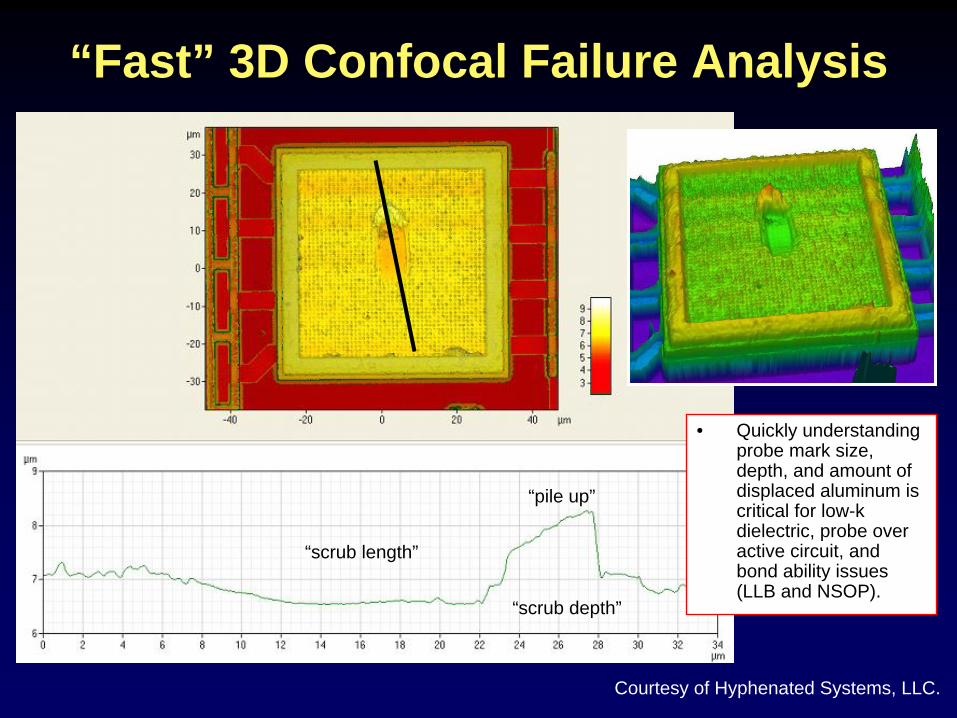
““FastFast”” 3D Confocal Failure Analysis3D Confocal Failure Analysis
“pile up”
“scrub depth”
“scrub length”
• Quickly understanding probe mark size, depth, and amount of displaced aluminum is critical for low-k dielectric, probe over active circuit, and bond ability issues (LLB and NSOP).
Courtesy of Hyphenated Systems, LLC.

Copper Metallization Makes TheCopper Metallization Makes The Problem Even Worse Problem Even Worse ……
New processes with smaller I/O pads needed smaller and sharper needles; increased chance to punch through the Al pad and expose copper
Exposed copper oxidizes fast and adversely effects the ball bonding
Exposed copper on I/O padOxidizes causing NSOP
Target Wire Bond

Punch ThroughPunch Through• Exposed copper identified with spectral analysis.
Punch Through Okay

Controlling the DamageControlling the Damage
• Continuous shrinkage in pad dimensions
• Thinner pad metal layer moving below 0.7um
• Lower k ILD structures
Metal (Al/Cu) Pad Metal Layer Thickness
Metal Layers/Vias
Low-k Dielectric
Al Probe Pad Cross-section View
Industry Requirements• Minimize yield loss due to
– Wire-bond reliability from deep scrub and large particles
– Probing damage at upper metal layers such as cracks
Probing Challenges
Wang, et al., SWTW-2007

Approaches to Damage ControlApproaches to Damage Control• The depth of the probe mark can be controlled
with by using alternate probe card technologies– Tip shape and probe geometry (various
manufacturers)– Low force probe cards (various manufacturers)– Optimized probe to pad interactions
• Probers can effectively change the z-stage motion just before contact and during overtravel to reduce damage– Variable Speed Probing by Accretech®– Micro-Touch™ by Electroglas®– 3D Probing by Tokyo Electron Limited® (TEL)

Pad Damage Versus TechnologyPad Damage Versus Technology
Cantilever
VerticalMembrane
Pad Surface
2000
1000
500 SCRUB HEIGHT
- 400 SCRUB DEPTH- 500
- 600/800- 1200Metal Thickness
nm
Courtesy of Infineon
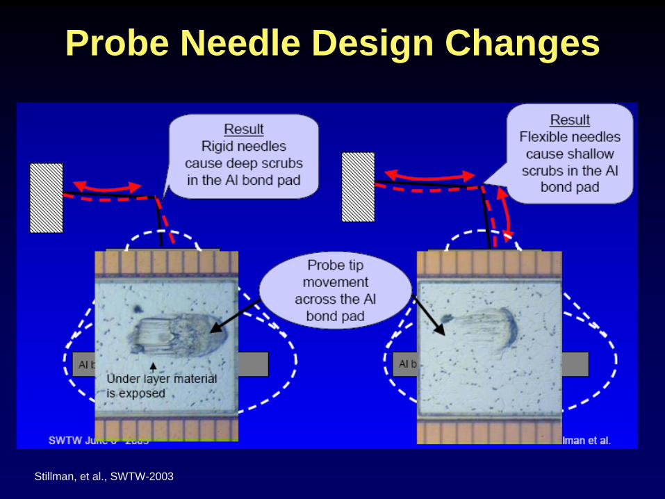
Probe Needle Design ChangesProbe Needle Design Changes
Stillman, et al., SWTW-2003
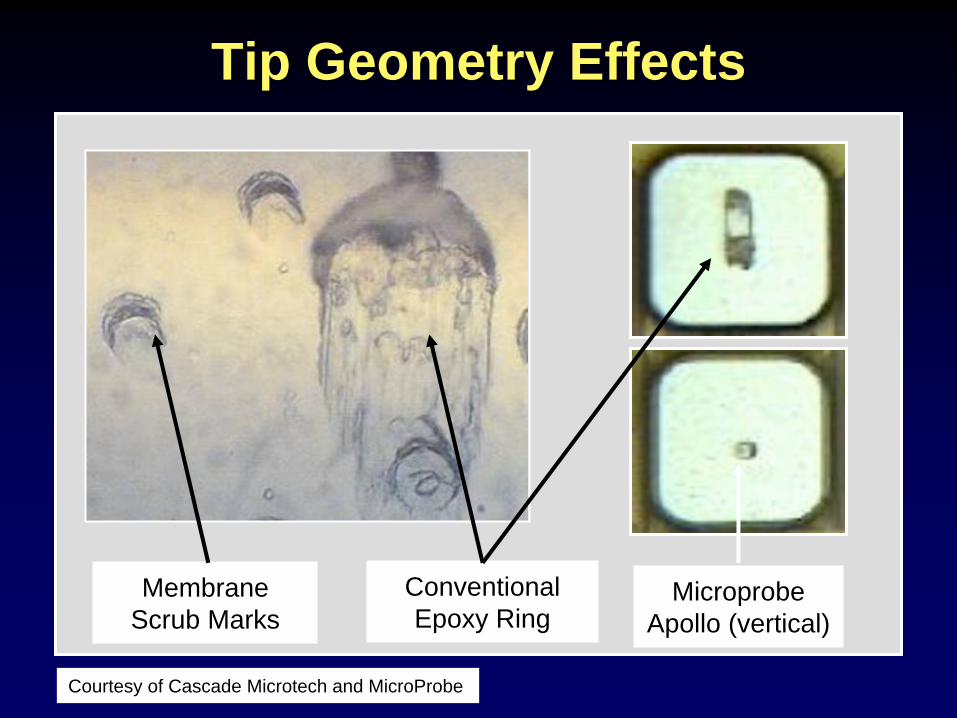
Tip Geometry EffectsTip Geometry Effects
Conventional Epoxy Ring
MembraneScrub Marks
MicroprobeApollo (vertical)
Courtesy of Cascade Microtech and MicroProbe

Reduced Probe GeometryReduced Probe Geometry• Reduce probe tip diameter• Reduce spring force and overdrive• Control number of probe passes
Benefits:• Smaller probe mark• Minimize probe size and depth
Concerns:• Probe card fabrication• Process control• Reduced card life
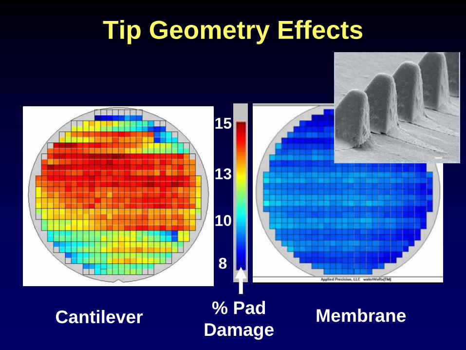
Tip Geometry EffectsTip Geometry Effects
Cantilever Membrane% Pad Damage
8
10
15
13

Advanced Scrub SensitivityAdvanced Scrub Sensitivity
• Macroscopically, punch through level was found to be a direct function of tip pressure– Tip area– Spring constant– Planarity – Over travel
Tip Size
Low High
Standard
Large
K
Wang, et al., SWTW-2007
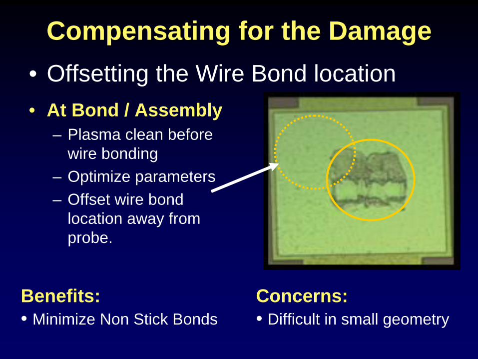
Compensating for the DamageCompensating for the Damage• Offsetting the Wire Bond location• At Bond / Assembly
– Plasma clean before wire bonding
– Optimize parameters– Offset wire bond
location away from probe.
Benefits:• Minimize Non Stick Bonds
Concerns:• Difficult in small geometry

Compensating for the DamageCompensating for the Damage• Elongated or Rectangular Pad Design
– Separate regions allocated for probe and bond
Probe Area Wire Bond AreaBenefits:• Separate probe and wire bond
Concerns:• May increase die size

Probe Over Passivation (POP)Probe Over Passivation (POP)• Eliminate probe and
wire bond interference• Creates longer bond
pad but it DID NOT increase die size– Requires 1 mask
change • Eliminate Cu exposure
due to heavy probe marks
• Ease of implementation on existing and new Cu technology products
Al Cap
Wire Bond Region
Cu padPassivation
Probe Region
Courtesy of Freescale Semiconductor

Benefits of Benefits of ““POPPOP””• Creates separate probe and wire bond regions without
die size increase
• Totally eliminates problem of punching through to Cu and interacting with wire bond– No damage of passivation or Cu after 6 double-touch passes at
heavy force and heavy overdrive – Achieved significant improvement in NSOP–
• New POP probe card specification can include higher spring force for better CRES performance during sort
• Numerous Freescale Cu devices at 50μm and finer pad pitches have switched to POP bond pad design
Prober Operation PerformanceProber Operation Performance
• Combination of vertical probe contact at over drive, coupled with horizontal chuck motion to minimize the probe mark damage
• Enabled by Intel, TEL and FormFactor for the MicroSpring™ card– Methodology designed to satisfy stringent
requirements for low-k ILD materials
• Resulted in 10:1 reduction of probe force with consistent and low contact resistance performance.
What Steps Can I Take ?What Steps Can I Take ?• Can reasonable steps be taken with existing
technologies (e.g., an existing probe card and a prober) to reduce pad damage in a cost-effective manner ?
• Is it possible to identify an optimized combination of prober operational settings to reduce the overall area and volumetric probe damage, i.e. disturbed pad area ?

Key Prober Operational SettingsKey Prober Operational Settings• Number of Touchdowns
– Single vs. Double
• Overtravel Magnitude– Low (50um) vs. Middle (63um) vs. High (75um)
• Undertravel Magnitude– Low (0um) vs. Middle (10um) vs. High (20um)
• Pin-Update Execution– Abbreviated pin alignment to compensate for thermal movement – On vs. Off
• Wafer Chuck Speed– Low (6000 um/sec) vs. High (18000 um/sec)
• Chuck Revise Execution– Re-zero of the wafer chuck to compensate for thermal movement– On vs. Off

Major Contributors to DamageMajor Contributors to Damage• Primary Responses for Area and Volume
– Single vs. Double Touchdown– Minimum vs. Maximum Overtravel
• Secondary Responses– Wafer chuck speed– Undertravel
• The influence of second order factors for fine-tuning the operational parameters can be performed using modeled response data.
• Other contributors for consideration– Small sample size effects– Operator-induced variability– Probe tip diameter variations– Probe gram force variations

50100150200250300
Mea
n(S
crub
Are
a)64
.055
95
±19.
7227
5
Dou
ble
Sin
gle
Singletd
Low
Hig
h
Lowspeed
Off
On
Offcr
50 63 75
50ot
10 20 off
10ut
Off
On
Onpu
0
20
40
60
Mea
n(D
ivot
Vol
ume)
8.73
2232
±8.4
3241
3
Dou
ble
Sing
le
Singletd
Low
Hig
h
Highspeed
Off
On
Oncr
50 63 75
50ot
10 20 off
20ut
Off
On
Onpu
Off
Best Case CombinationsBest Case CombinationsModeled response data can be used to investigate the effects of changing one parameter and keeping the other constant.
– Slopes of the lines can give some indication of sensitivity to the change.
Number of TDs Overtravel Miller, et al., SWTW-2007

Effects of Effects of ReprobeReprobe on Pad Damageon Pad Damage
AaA s
TD
nnd ∑
=−=
11
1
Intuitively we know the 2D effects of reprobe or multiple probe steps diminish with each touchdown but at what rate?
One model:Where:
Ad - disturbed area
TD - touchdowns
a - scaling coefficient
As - scrub mark 2D size

Pad Damage: Actual Versus ModelPad Damage: Actual Versus Model
DoE• multiple wafers• one probe card• one test cell• one operator• same setup each time• fully disturbed wafers
The goal of the design of experiment would be to hold everything constant and only change the number of touchdowns.
• fully disturbed probe card
• seven cumulative touchdowns
Millions of scrub marks!
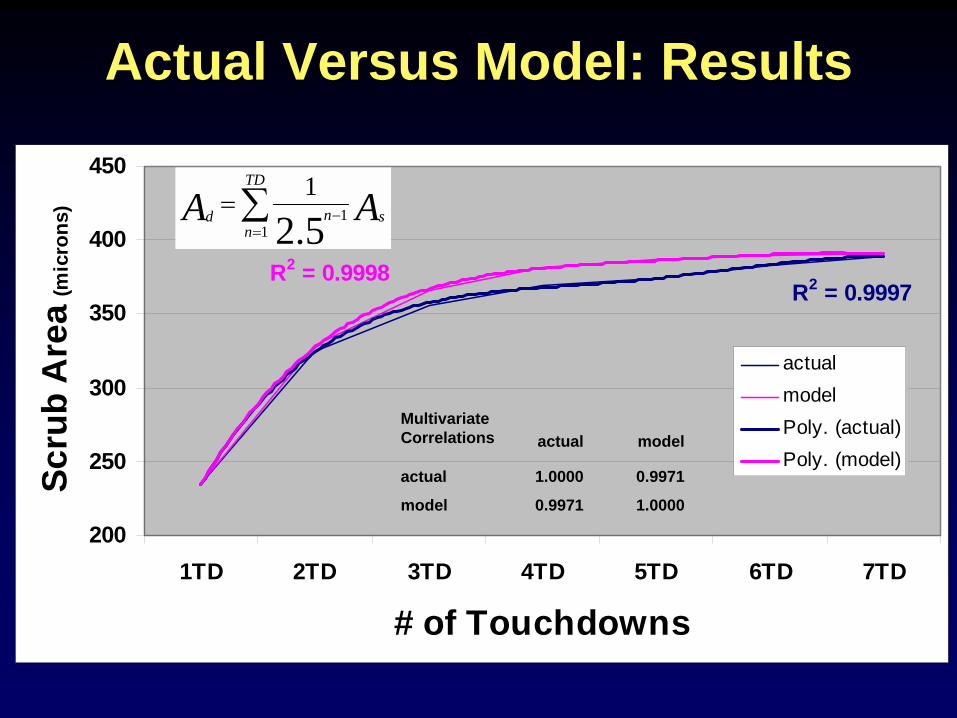
Actual Versus Model: ResultsActual Versus Model: Results
R2 = 0.9997R2 = 0.9998
200
250
300
350
400
450
1TD 2TD 3TD 4TD 5TD 6TD 7TD
# of Touchdowns
Scru
b A
rea
(mic
rons
)
actualmodelPoly. (actual)Poly. (model)
AA s
TD
nnd ∑
=−=
115.2
1
Multivariate Correlations actual model
actual 1.0000 0.9971
model 0.9971 1.0000

Tip treatment[B]Tip size[Large]TD count[Five]Tip treatment[A]Tip size[Large]*Tip treatment[B]Tip shape[1]*Tip treatment[B]TD count[Five]*Tip treatment[A]Tip size[Large]*TD count[Five]Tip size[Large]*Tip treatment[A]Tip shape[1]TD count[Five]*Tip treatment[B]Tip shape[1]*Tip treatment[A]TD count[Five]*Tip shape[1]Tip size[Large]*Tip shape[1]
Term -15.99093 -10.28125 6.95375 -3.80436 -2.77981 2.66668 -2.59187 -2.19958 -2.06523 2.06375 1.71031 1.01195 -0.50792 0.10375
Orthog Estimate
Pareto Plot of Transformed Estimates
Scrub Sensitivity Analysis DOEScrub Sensitivity Analysis DOE Results: Results: ““Scrub DepthScrub Depth”” Pareto PlotPareto Plot
Significant factors for scrub depth: Tip conditions, tip size, TD count, and Interactions
t ratio > 3.0
Wang, et al., SWTW-2007

-10205080
110
Scr
ub d
epth
met
ric (%
)
-10205080
110
Scr
ub d
epth
met
ric (%
)
-10205080
110
Scr
ub d
epth
met
ric (%
)
-10205080
110
Scr
ub d
epth
met
ric (%
)Tip size
FiveOne
12
ABC
Large Small
LargeSmall
TD count
12
A
B
C
Five One
LargeSmall
FiveOne
Tip shape
A
B
C
1 2
LargeSmall
FiveOne
12
Tiptreatment
A B C
Tip sizeTD
countTip shape
Tip treatment
Interaction Profiles
Scrub Sensitivity Analysis DOEScrub Sensitivity Analysis DOE Results: Results: ““Scrub DepthScrub Depth”” Interaction Interaction
ProfileProfile
Macroscopic Microscopic
Macroscopic, microscopic factors and their interactions all impact scrub depthWang, et al., SWTW-2007

Tip treatment[B]Tip size[Large]TD count[Five]Tip treatment[A]Tip size[Large]*Tip treatment[B]Tip shape[1]*Tip treatment[B]TD count[Five]*Tip treatment[A]Tip size[Large]*TD count[Five]Tip size[Large]*Tip treatment[A]Tip shape[1]TD count[Five]*Tip treatment[B]Tip shape[1]*Tip treatment[A]TD count[Five]*Tip shape[1]Tip size[Large]*Tip shape[1]
Term -15.99093 -10.28125 6.95375 -3.80436 -2.77981 2.66668 -2.59187 -2.19958 -2.06523 2.06375 1.71031 1.01195 -0.50792 0.10375
Orthog Estimate
Pareto Plot of Transformed Estimates
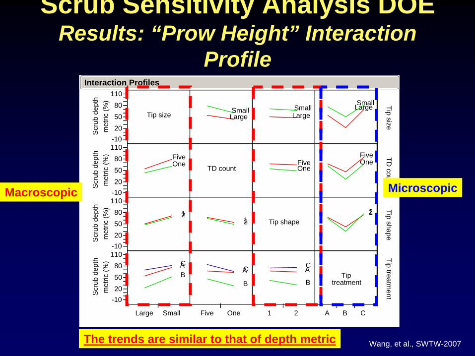
Scrub Sensitivity Analysis DOEScrub Sensitivity Analysis DOE Results: Results: ““Prow HeightProw Height”” Pareto PlotPareto Plot
TD count, tip conditions, and tip size all contribute to the prow height metric
t ratio > 3.0
Wang, et al., SWTW-2007
-10205080
110S
crub
dep
thm
etric
(%)
-10205080
110
Scr
ub d
epth
met
ric (%
)
-10205080
110
Scr
ub d
epth
met
ric (%
)
-10205080
110
Scr
ub d
epth
met
ric (%
)Tip size
FiveOne
12
ABC
Large Small
LargeSmall
TD count
12
A
B
C
Five One
LargeSmall
FiveOne
Tip shape
A
B
C
1 2
LargeSmall
FiveOne
12
Tiptreatment
A B C
Tip sizeTD
countTip shape
Tip treatment
Interaction Profiles
Scrub Sensitivity Analysis DOEScrub Sensitivity Analysis DOE Results: Results: ““Prow HeightProw Height”” Interaction Interaction
ProfileProfile
Macroscopic Microscopic
The trends are similar to that of depth metric Wang, et al., SWTW-2007

Hartfield, et al., SWTW-2004
Conventional Cantilever Design Considerations
SummarySummary• I/O pad damage has been aggravated by smaller pads,
sharper needles, and new process node technologies.
• Changes and improvements to probe card specification have been developed to mitigate some of the problems.
• Significant new probe methods, new probe card technologies, and design and layout tricks are now being implemented.
• Reasonable steps can be taken with “existing” hardware to reduce pad damage in a cost-effective manner.

AcknowledgementsAcknowledgements• Special thanks to Dr. Jerry Broz and Bill
Mann for their significant contribution!!!• Thanks to the SWTW Program Committee
for their contribution and critique