packaging and ball bonding gold wire makes contact …glennc/e495/e495l13l.pdf · packaging and...
TRANSCRIPT

Packaging and Ball Bonding Gold wire makes contact from bonding pads on chip to package Gold wire is formed into ball to make contact Uses an ultrasonic process & heat Process called "Ball Bonding"

Wedge Bonding Use also gold wire Flatten wire Wedge usually on package, ball on chip Note wire elevated above surface

Basic Ball Bonding Ball on chip Wedge on package

Wires on Package Close spacing of wires difficult with high pin count Limitation is set by angle the bonds must come in at

Ball Bonder Cycle (a) Start with ball on wire in anvil (capillary) over pad (b) Anvil presses ball onto pad with ultrasonic to create bond (c) Release with and move vertically (d) Move wire to lead pad on package (e & f) Create wedge bond at lead with anvil & break wire (g) Spark melts wire to create new ball
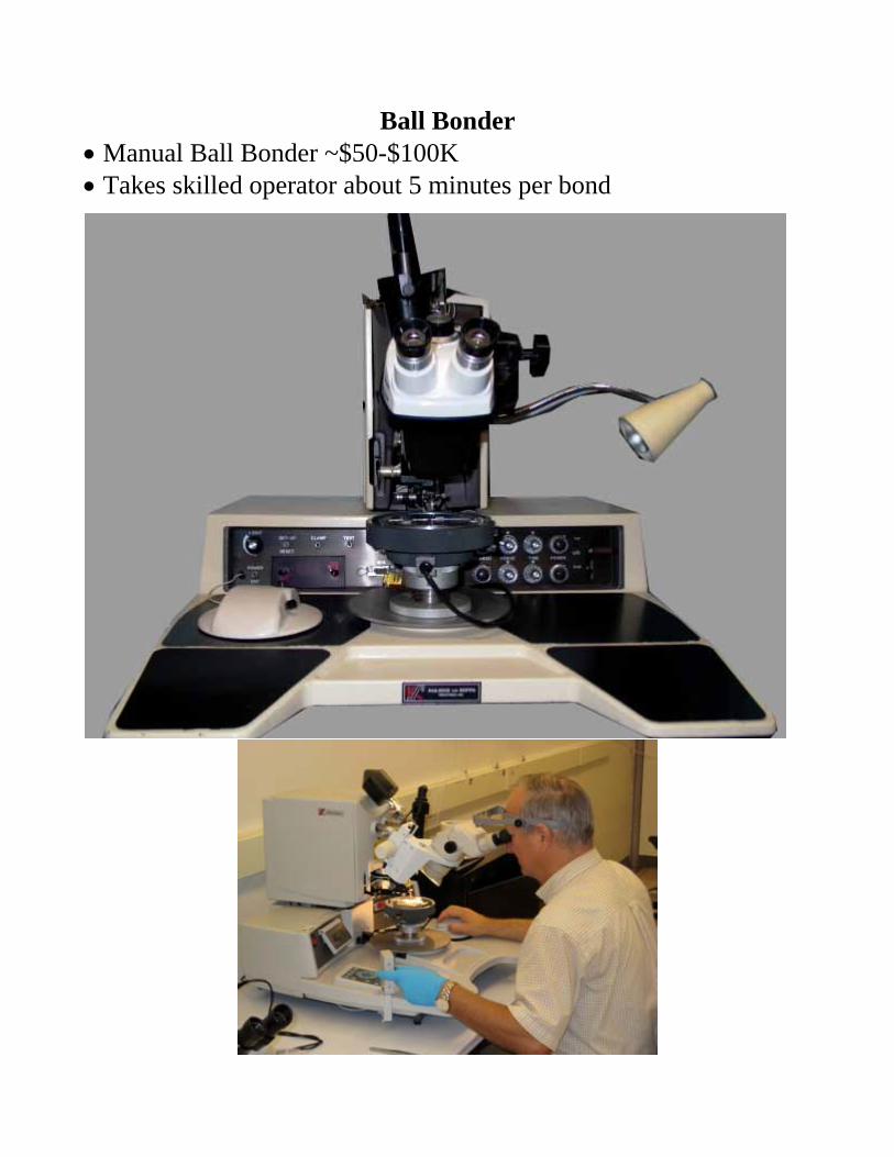
Ball Bonder Manual Ball Bonder ~$50-$100K Takes skilled operator about 5 minutes per bond

Head Movement in Ball & Wedge Bonder Ball bonder head moves x, y, z Wedge bonder head moves only z, stage x,y
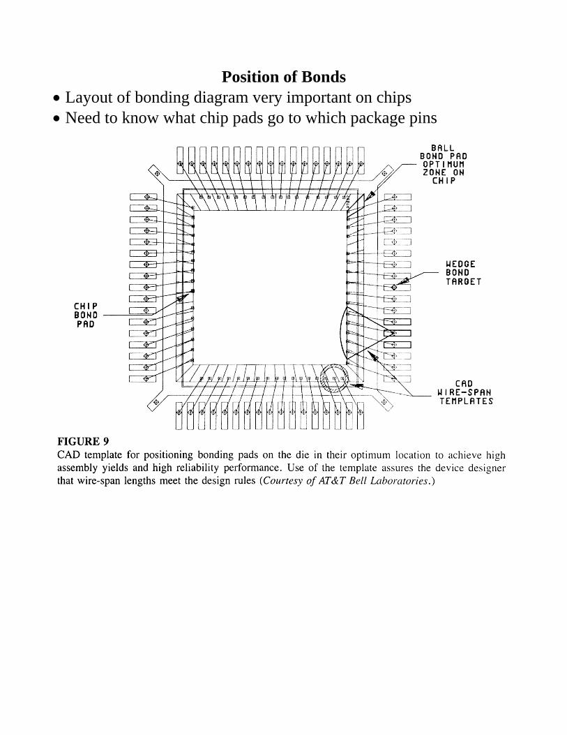
Position of Bonds Layout of bonding diagram very important on chips Need to know what chip pads go to which package pins

Angle Limitations on Bonds Angle of bonds determines limit of bonding possibility

Corners of Chips: Problem bonding area Corners where bonds often limited

Microprocessors, Logic & Bond Count increase DRAM pin count is steady due to multiplexing of addresses Enhanced by use of SIM modules Microprocessor and Logic tend towards Rent’s rule
CountGatePinsIO
Typically: =4.5, =0.5

Other Bonding Tape Automated Bonding: All bonds at once Flip Chip Indium solder ball mounting

Vertical Buried Collector Bipolar Process Put buried collector to reduce collector resistance

Standard Buried Collector (SBC) Bipolar Process Start with P substrate, high resistance Grow oxide, mask for buried collector n+ buried layer implant Grow n type epi layer Mask for P type isolation diffusion to P substrate

Buried Collector Bipolar Isolation & Base Grow oxide, and mask for p base Grow oxide, mask for n+ emitter & collector contact Deposit and pattern metal

Buried Collector (SBC) Bipolar Emitter/Collector

Simple MosFet Transistor Need to create a isolated gate between source & drain Originally metal gate, now all polygate

Simple One Metal/poly MosFet Simple One metal/poly MosFet

Simple One Metal/poly MosFet Simple One metal/poly MosFet Con'd

CMC Double metal, single poly CMOS

CMC CMOS: Poly through Metal

CMOS Design Rules Sets size limits on structures Depends on the Design
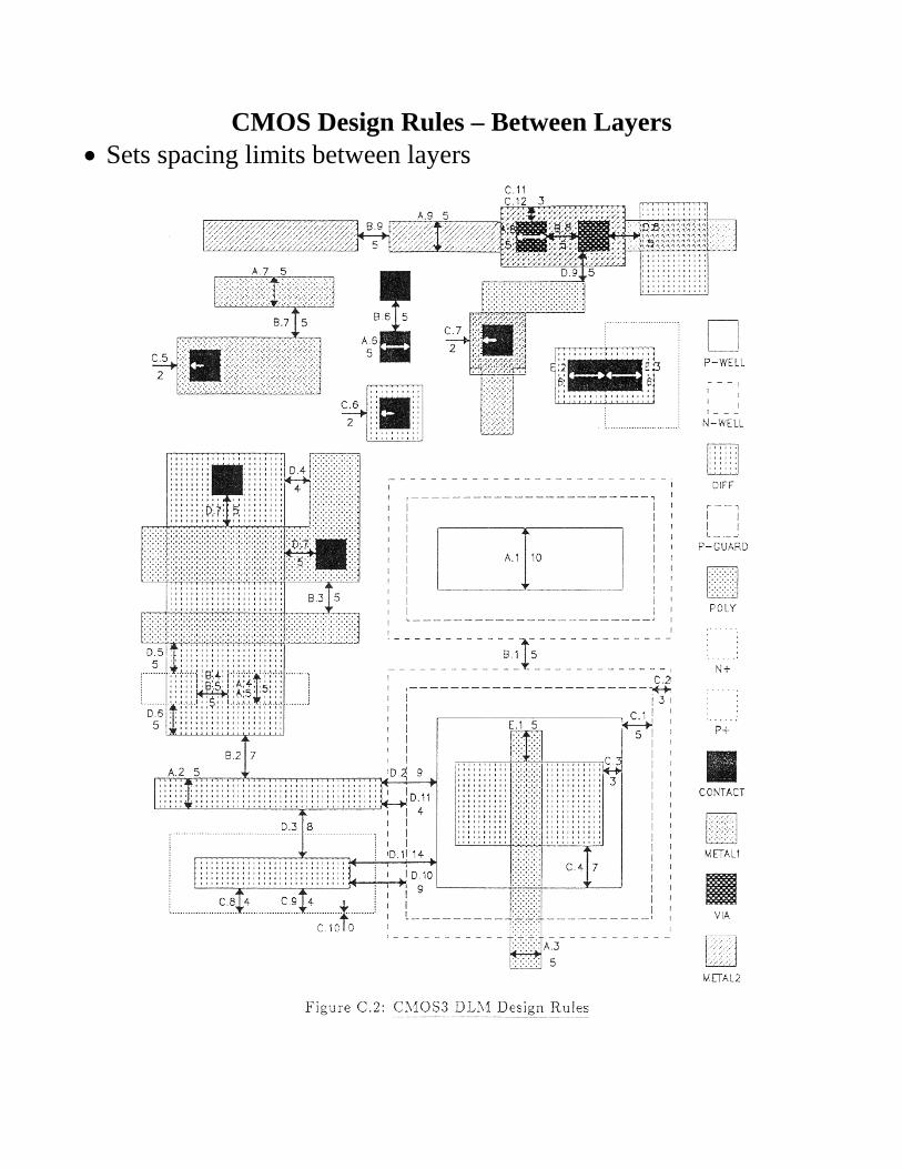
CMOS Design Rules – Between Layers Sets spacing limits between layers

CMOS Design Rules – Bonding Pads Bonding pads also have rules
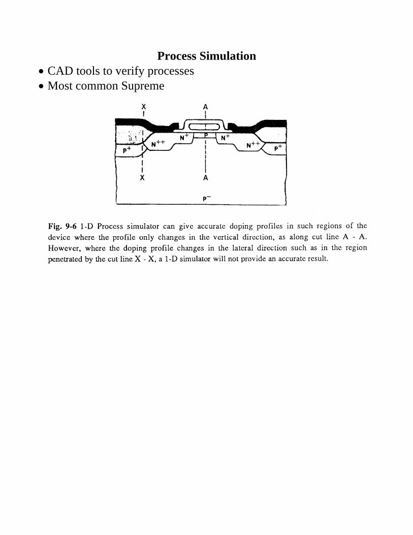
Process Simulation CAD tools to verify processes Most common Supreme

SUPREM Stanford University PRocess Engineering Model Now available from several commercial sources, Synopsys Added graphic interface

Supreme Block Diagram Simple form: write text file description Still retains "cards": actually lines Useful when doing unique process When using specified process – design structure with Cadence Use fabrication technology that specifies steps eg CMOS18 (180 nm process)

1 Dimensional Supreme Input

1 Dimensional Supreme Input

2D Supreme Must create Grid High density in important areas

2D Supreme Output: Locos process Can simulate Local Oxidation process (SiN patterning of oxide) Diffusion of oxygen & stress in SiN show shape of oxide

Trench Capacitors in Supreme IV Simulate full etch and deposition processes