p89lpc932a1 8-bit microcontroller with accelerated … 8 kb byte-erasable flash code memory...
TRANSCRIPT
1. General description
The P89LPC932A1 is a single-chip microcontroller, available in low cost packages, basedon a high performance processor architecture that executes instructions in two to fourclocks, six times the rate of standard 80C51 devices. Many system-level functions havebeen incorporated into the P89LPC932A1 in order to reduce component count, boardspace, and system cost.
2. Features
2.1 Principal featuresn 8 kB byte-erasable flash code memory organized into 1 kB sectors and 64-byte pages.
Single-byte erasing allows any byte(s) to be used as non-volatile data storage.
n 256-byte RAM data memory, 512-byte auxiliary on-chip RAM.
n 512-byte customer data EEPROM on chip allows serialization of devices, storage ofset-up parameters, etc.
n Two analog comparators with selectable inputs and reference source.
n Two 16-bit counter/timers (each may be configured to toggle a port output upon timeroverflow or to become a PWM output) and a 23-bit system timer that can also be usedas a RTC.
n Enhanced UART with fractional baud rate generator, break detect, framing errordetection, and automatic address detection; 400 kHz byte-wide I2C-buscommunication port and SPI communication port.
n CCU provides PWM, input capture, and output compare functions.
n High-accuracy internal RC oscillator option allows operation without external oscillatorcomponents. The RC oscillator option is selectable and fine tunable.
n 2.4 V to 3.6 V VDD operating range. I/O pins are 5 V tolerant (may be pulled up ordriven to 5.5 V).
n 28-pin TSSOP, PLCC, HVQFN, and DIP packages with 23 I/O pins minimum and up to26 I/O pins while using on-chip oscillator and reset options.
2.2 Additional featuresn A high performance 80C51 CPU provides instruction cycle times of 111 ns to 222 ns
for all instructions except multiply and divide when executing at 18 MHz. This is sixtimes the performance of the standard 80C51 running at the same clock frequency. Alower clock frequency for the same performance results in power savings and reducedEMI.
P89LPC932A18-bit microcontroller with accelerated two-clock 80C51 core8 kB 3 V byte-erasable flash with 512-byte data EEPROMRev. 03 — 12 March 2007 Product data sheet
NXP Semiconductors P89LPC932A18-bit microcontroller with accelerated two-clock 80C51 core
n In-Circuit Programming (ICP) allows simple production coding with commercialEPROM programmers. Flash security bits prevent reading of sensitive applicationprograms.
n Serial flash In-System Programming (ISP) allows coding while the device is mountedin the end application.
n In-Application Programming (IAP) of the flash code memory. This allows changing thecode in a running application.
n Watchdog timer with separate on-chip oscillator, requiring no external components.The watchdog prescaler is selectable from eight values.
n Low voltage reset (brownout detect) allows a graceful system shutdown when powerfails. May optionally be configured as an interrupt.
n Idle and two different power-down reduced power modes. Improved wake-up fromPower-down mode (a LOW interrupt input starts execution). Typical power-downcurrent is 1 µA (total power-down with voltage comparators disabled).
n Active-LOW reset. On-chip power-on reset allows operation without external resetcomponents. A reset counter and reset glitch suppression circuitry prevent spuriousand incomplete resets. A software reset function is also available.
n Configurable on-chip oscillator with frequency range options selected by userprogrammed flash configuration bits. Oscillator options support frequencies from20 kHz to the maximum operating frequency of 18 MHz.
n Oscillator fail detect. The watchdog timer has a separate fully on-chip oscillatorallowing it to perform an oscillator fail detect function.
n Programmable port output configuration options: quasi-bidirectional, open drain,push-pull, input-only.
n Port ‘input pattern match’ detect. Port 0 may generate an interrupt when the value ofthe pins match or do not match a programmable pattern.
n LED drive capability (20 mA) on all port pins. A maximum limit is specified for theentire chip.
n Controlled slew rate port outputs to reduce EMI. Outputs have approximately 10 nsminimum ramp times.
n Only power and ground connections are required to operate the P89LPC932A1 wheninternal reset option is selected.
n Four interrupt priority levels.
n Eight keypad interrupt inputs, plus two additional external interrupt inputs.
n Schmitt trigger port inputs.
n Second data pointer.
n Emulation support.
2.3 Comparison to the P89LPC932The P89LPC932A1 includes several improvements compared to the P89LPC932. Pleasesee P89LPC932A1 User manual for additional detailed information.
n Byte-erasability has been added to the user code memory space.
n All of the errata described in the P89LPC932 Errata sheet have been fixed.
n Serial ICP has been added.
P89LPC932A1_3 © NXP B.V. 2007. All rights reserved.
Product data sheet Rev. 03 — 12 March 2007 2 of 64
NXP Semiconductors P89LPC932A18-bit microcontroller with accelerated two-clock 80C51 core
n The RCCLK bit has been added to the TRIM register allowing the RCCLK to beselected as the CPU clock (CCLK) regardless of the settings in UCFG1, allowing theinternal RC oscillator to be selected as the CPU clock without the need to reset thedevice.
n Enhancements added to the ISP/IAP code to improve code safety and increaseISP/IAP functionality. This may require slight changes to original P89LPC932 codeusing IAP function calls. Some ISP/IAP settings are different than the originalP89LPC932. Tools designed to support the P89LPC932A1 should be used to programthis device, such as Flash Magic version 1.98, or later.
3. Ordering information
Table 1. Ordering information
Type number Package
Name Description Version
P89LPC932A1FA PLCC28 plastic leaded chip carrier; 28 leads SOT261-2
P89LPC932A1FDH TSSOP28 plastic thin shrink small outline package; 28 leads; body width4.4 mm
SOT361-1
P89LPC932A1FHN HVQFN28 plastic thermal enhanced very thin quad flat package; no leads;28 terminals; body 6 × 6 × 0.85 mm
SOT788-1
P89LPC932A1FN DIP28 plastic dual in-line package; 28 leads (600 mil) SOT117-1
P89LPC932A1_3 © NXP B.V. 2007. All rights reserved.
Product data sheet Rev. 03 — 12 March 2007 3 of 64
NXP Semiconductors P89LPC932A18-bit microcontroller with accelerated two-clock 80C51 core
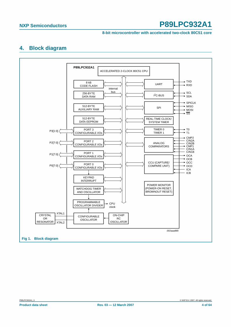
4. Block diagram
Fig 1. Block diagram
ACCELERATED 2-CLOCK 80C51 CPU
8 kBCODE FLASH
256-BYTEDATA RAM
PORT 2CONFIGURABLE I/Os
PORT 1CONFIGURABLE I/Os
PORT 0CONFIGURABLE I/Os
KEYPADINTERRUPT
PROGRAMMABLEOSCILLATOR DIVIDER
CPUclock
CONFIGURABLEOSCILLATOR
ON-CHIPRC
OSCILLATOR
internalbus
CRYSTALOR
RESONATOR
POWER MONITOR(POWER-ON RESET, BROWNOUT RESET)
002aaa885
UART
ANALOGCOMPARATORS
512-BYTEAUXILIARY RAM
I2C-BUS
512-BYTEDATA EEPROM
PORT 3CONFIGURABLE I/Os
CCU (CAPTURE/COMPARE UNIT)
P89LPC932A1
WATCHDOG TIMERAND OSCILLATOR
TIMER 0TIMER 1
REAL-TIME CLOCK/SYSTEM TIMER
SPI
P3[1:0]
P2[7:0]
P1[7:0]
P0[7:0]
XTAL1
XTAL2
TXDRXD
SCLSDA
SPICLKMISOMOSISS
T0T1
CMP2CIN2ACIN2BCMP1CIN1ACIN1BOCAOCBOCCOCDICAICB
P89LPC932A1_3 © NXP B.V. 2007. All rights reserved.
Product data sheet Rev. 03 — 12 March 2007 4 of 64
NXP Semiconductors P89LPC932A18-bit microcontroller with accelerated two-clock 80C51 core
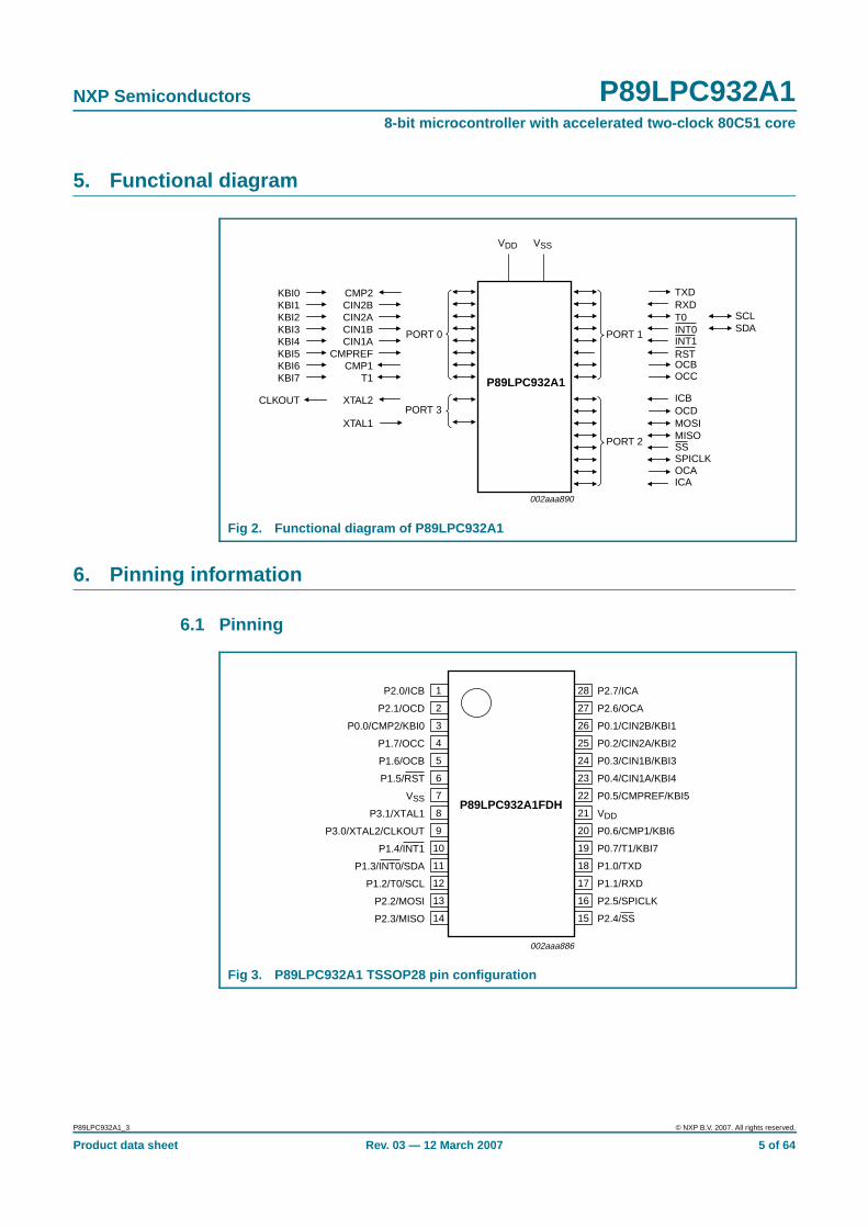
5. Functional diagram
6. Pinning information
6.1 Pinning
Fig 2. Functional diagram of P89LPC932A1
VDD VSS
PORT 0
PORT 3
TXDRXDT0INT0INT1RST
SCLSDA
002aaa890
CMP2CIN2BCIN2ACIN1BCIN1A
CMPREFCMP1
T1
XTAL2
XTAL1
KBI0KBI1KBI2KBI3KBI4KBI5KBI6KBI7
CLKOUT
OCBOCC
ICBOCDMOSIMISOSSSPICLKOCAICA
PORT 1
PORT 2
P89LPC932A1
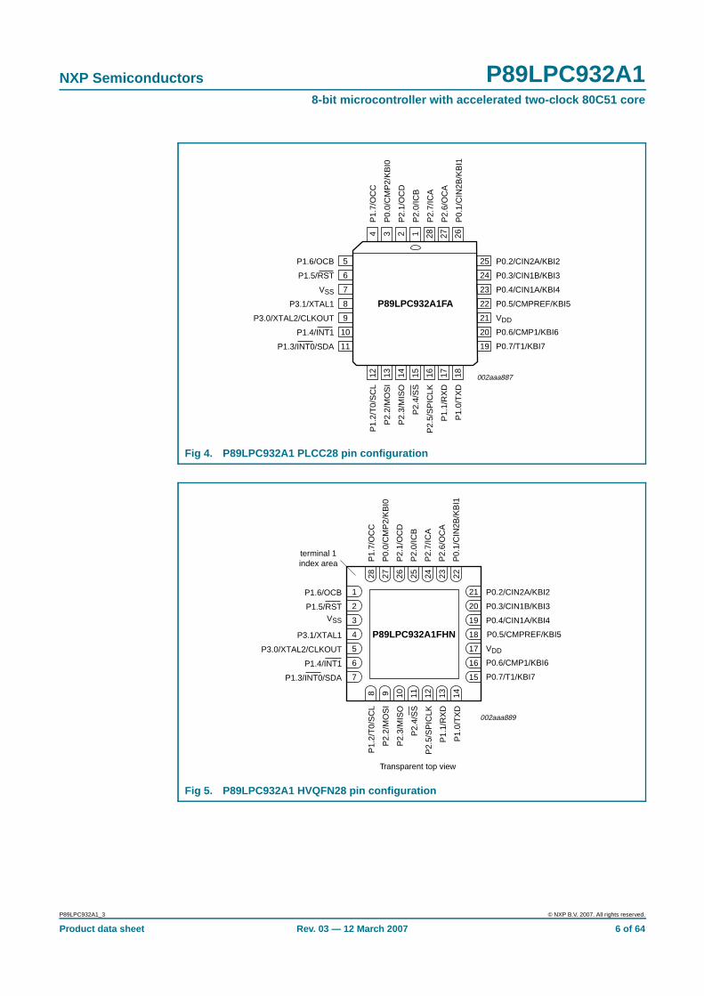
Fig 3. P89LPC932A1 TSSOP28 pin configuration
P89LPC932A1FDH
002aaa886
1
2
3
4
5
6
7
8
9
10
11
12
13
14
16
15
18
17
20
19
22
21
24
23
26
25
28
27
P2.7/ICA
P2.6/OCA
P0.1/CIN2B/KBI1
P0.2/CIN2A/KBI2
P0.3/CIN1B/KBI3
P0.4/CIN1A/KBI4
P0.5/CMPREF/KBI5
VDD
P0.6/CMP1/KBI6
P0.7/T1/KBI7
P1.0/TXD
P1.1/RXD
P2.5/SPICLK
P2.4/SS
P2.0/ICB
P2.1/OCD
P0.0/CMP2/KBI0
P1.7/OCC
P1.6/OCB
P1.5/RST
VSS
P3.1/XTAL1
P3.0/XTAL2/CLKOUT
P1.4/INT1
P1.3/INT0/SDA
P1.2/T0/SCL
P2.2/MOSI
P2.3/MISO
P89LPC932A1_3 © NXP B.V. 2007. All rights reserved.
Product data sheet Rev. 03 — 12 March 2007 5 of 64
NXP Semiconductors P89LPC932A18-bit microcontroller with accelerated two-clock 80C51 core
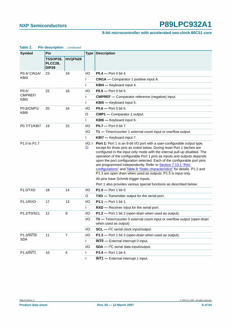
Fig 4. P89LPC932A1 PLCC28 pin configuration
Fig 5. P89LPC932A1 HVQFN28 pin configuration
P89LPC932A1FA
002aaa887
5
6
7
8
9
10
11
25
24
23
22
21
20
19
12 13 14 15 16 17 18
4 3 2 1 28 27 26
P1.6/OCB
P1.5/RST
VSS
P3.1/XTAL1
P3.0/XTAL2/CLKOUT
P1.4/INT1
P1.3/INT0/SDA
P1.
7/O
CC
P0.
0/C
MP
2/K
BI0
P2.
1/O
CD
P2.
0/IC
B
P2.
7/IC
A
P2.
6/O
CA
P0.
1/C
IN2B
/KB
I1
P0.2/CIN2A/KBI2
P0.3/CIN1B/KBI3
P0.4/CIN1A/KBI4
P0.5/CMPREF/KBI5
VDD
P0.6/CMP1/KBI6
P0.7/T1/KBI7
P1.
2/T
0/S
CL
P2.
2/M
OS
I
P2.
3/M
ISO
P2.
4/S
S
P2.
5/S
PIC
LK
P1.
1/R
XD
P1.
0/T
XD
002aaa889
P89LPC932A1FHN
Transparent top view
7 15
6 16
5 17
4 18
3 19
2 20
1 21
8 9 10 11 12 13 14
28 27 26 25 24 23 22
terminal 1index area P
1.7/
OC
C
P2.
7/IC
A
P2.
1/O
CD
P2.
0/IC
B
P0.
0/C
MP
2/K
BI0
P2.
6/O
CA
P0.
1/C
IN2B
/KB
I1
P2.
4/S
S
P2.
2/M
OS
I
P2.
3/M
ISO
P1.
2/T
0/S
CL
P2.
5/S
PIC
LK
P1.
0/T
XD
P1.
1/R
XD
P1.4/INT1
P1.3/INT0/SDA
P3.0/XTAL2/CLKOUT
P3.1/XTAL1
VSS
P1.5/RST
P1.6/OCB
P0.6/CMP1/KBI6
P0.7/T1/KBI7
P0.5/CMPREF/KBI5
VDD
P0.4/CIN1A/KBI4
P0.3/CIN1B/KBI3
P0.2/CIN2A/KBI2
P89LPC932A1_3 © NXP B.V. 2007. All rights reserved.
Product data sheet Rev. 03 — 12 March 2007 6 of 64

NXP Semiconductors P89LPC932A18-bit microcontroller with accelerated two-clock 80C51 core
6.2 Pin description
Fig 6. P89LPC932A1 DIP28 pin configuration
P89LPC932A1FN
002aac785
1
2
3
4
5
6
7
8
9
10
11
12
13
14
16
15
18
17
20
19
22
21
24
23
26
25
28
27
P2.0/ICB
P2.1/OCD
P0.0/CMP2/KBI0
P1.7/OCC
P1.6/OCB
P1.5/RST
VSS
P3.1/XTAL1
P3.0/XTAL2/CLKOUT
P1.4/INT1
P1.3/INT0/SDA
P1.2/T0/SCL
P2.2/MOSI
P2.3/MISO
P2.7/ICA
P2.6/OCA
P0.1/CIN2B/KBI1
P0.2/CIN2A/KBI2
P0.3/CIN1B/KBI3
P0.4/CIN1A/KBI4
P0.5/CMPREF/KBI5
VDD
P0.6/CMP1/KBI6
P0.7/T1/KBI7
P1.0/TXD
P1.1/RXD
P2.5/SPICLK
P2.4/SS
Table 2. Pin description
Symbol Pin Type Description
TSSOP28,PLCC28,DIP28
HVQFN28
P0.0 to P0.7 I/O Port 0: Port 0 is an 8-bit I/O port with a user-configurable output type.During reset Port 0 latches are configured in the input only mode with theinternal pull-up disabled. The operation of Port 0 pins as inputs andoutputs depends upon the port configuration selected. Each port pin isconfigured independently. Refer to Section 7.13.1 “Port configurations”and Table 8 “Static characteristics” for details.
The Keypad Interrupt feature operates with Port 0 pins.
All pins have Schmitt trigger inputs.
Port 0 also provides various special functions as described below:
P0.0/CMP2/KBI0
3 27 I/O P0.0 — Port 0 bit 0.
O CMP2 — Comparator 2 output.
I KBI0 — Keyboard input 0.
P0.1/CIN2B/KBI1
26 22 I/O P0.1 — Port 0 bit 1.
I CIN2B — Comparator 2 positive input B.
I KBI1 — Keyboard input 1.
P0.2/CIN2A/KBI2
25 21 I/O P0.2 — Port 0 bit 2.
I CIN2A — Comparator 2 positive input A.
I KBI2 — Keyboard input 2.
P0.3/CIN1B/KBI3
24 20 I/O P0.3 — Port 0 bit 3.
I CIN1B — Comparator 1 positive input B.
I KBI3 — Keyboard input 3.
P89LPC932A1_3 © NXP B.V. 2007. All rights reserved.
Product data sheet Rev. 03 — 12 March 2007 7 of 64
NXP Semiconductors P89LPC932A18-bit microcontroller with accelerated two-clock 80C51 core
P0.4/ CIN1A/KBI4
23 19 I/O P0.4 — Port 0 bit 4.
I CIN1A — Comparator 1 positive input A.
I KBI4 — Keyboard input 4.
P0.5/CMPREF/KBI5
22 18 I/O P0.5 — Port 0 bit 5.
I CMPREF — Comparator reference (negative) input.
I KBI5 — Keyboard input 5.
P0.6/CMP1/KBI6
20 16 I/O P0.6 — Port 0 bit 6.
O CMP1 — Comparator 1 output.
I KBI6 — Keyboard input 6.
P0.7/T1/KBI7 19 15 I/O P0.7 — Port 0 bit 7.
I/O T1 — Timer/counter 1 external count input or overflow output.
I KBI7 — Keyboard input 7.
P1.0 to P1.7 I/O, I[1]
Port 1: Port 1 is an 8-bit I/O port with a user-configurable output type,except for three pins as noted below. During reset Port 1 latches areconfigured in the input only mode with the internal pull-up disabled. Theoperation of the configurable Port 1 pins as inputs and outputs dependsupon the port configuration selected. Each of the configurable port pinsare programmed independently. Refer to Section 7.13.1 “Portconfigurations” and Table 8 “Static characteristics” for details. P1.2 andP1.3 are open drain when used as outputs. P1.5 is input only.
All pins have Schmitt trigger inputs.
Port 1 also provides various special functions as described below:
P1.0/TXD 18 14 I/O P1.0 — Port 1 bit 0.
O TXD — Transmitter output for the serial port.
P1.1/RXD 17 13 I/O P1.1 — Port 1 bit 1.
I RXD — Receiver input for the serial port.
P1.2/T0/SCL 12 8 I/O P1.2 — Port 1 bit 2 (open-drain when used as output).
I/O T0 — Timer/counter 0 external count input or overflow output (open-drainwhen used as output).
I/O SCL — I2C serial clock input/output.
P1.3/INT0/SDA
11 7 I/O P1.3 — Port 1 bit 3 (open-drain when used as output).
I INT0 — External interrupt 0 input.
I/O SDA — I2C serial data input/output.
P1.4/INT1 10 6 I P1.4 — Port 1 bit 4.
I INT1 — External interrupt 1 input.
Table 2. Pin description …continued
Symbol Pin Type Description
TSSOP28,PLCC28,DIP28
HVQFN28
P89LPC932A1_3 © NXP B.V. 2007. All rights reserved.
Product data sheet Rev. 03 — 12 March 2007 8 of 64
NXP Semiconductors P89LPC932A18-bit microcontroller with accelerated two-clock 80C51 core
P1.5/RST 6 2 I P1.5 — Port 1 bit 5 (input only).
I RST — External Reset input during power-on or if selected via UCFG1.When functioning as a reset input, a LOW on this pin resets themicrocontroller, causing I/O ports and peripherals to take on their defaultstates, and the processor begins execution at address 0. Also used duringa power-on sequence to force ISP mode. When using an oscillatorfrequency above 12 MHz, the reset input function of P1.5 must beenabled. An external circuit is required to hold the device in reset atpower-up until V DD has reached its specified level. When systempower is removed V DD will fall below the minimum specifiedoperating voltage. When using an oscillator frequency above12 MHz, in some applications, an external brownout detect circuitmay be required to hold the device in reset when V DD falls below theminimum specified operating voltage.
P1.6/OCB 5 1 I/O P1.6 — Port 1 bit 6.
O OCB — Output Compare B.
P1.7/OCC 4 28 I/O P1.7 — Port 1 bit 7.
O OCC — Output Compare C.
P2.0 to P2.7 I/O Port 2: Port 2 is an 8-bit I/O port with a user-configurable output type.During reset Port 2 latches are configured in the input only mode with theinternal pull-up disabled. The operation of Port 2 pins as inputs andoutputs depends upon the port configuration selected. Each port pin isconfigured independently. Refer to Section 7.13.1 “Port configurations”and Table 8 “Static characteristics” for details.
All pins have Schmitt trigger inputs.
Port 2 also provides various special functions as described below:
P2.0/ICB 1 25 I/O P2.0 — Port 2 bit 0.
I ICB — Input Capture B.
P2.1/OCD 2 26 I/O P2.1 — Port 2 bit 1.
O OCD — Output Compare D.
P2.2/MOSI 13 9 I/O P2.2 — Port 2 bit 2.
I/O MOSI — SPI master out slave in. When configured as master, this pin isoutput; when configured as slave, this pin is input.
P2.3/MISO 14 10 I/O P2.3 — Port 2 bit 3.
I/O MISO — When configured as master, this pin is input, when configured asslave, this pin is output.
P2.4/SS 15 11 I/O P2.4 — Port 2 bit 4.
I SS — SPI Slave select.
P2.5/SPICLK 16 12 I/O P2.5 — Port 2 bit 5.
I/O SPICLK — SPI clock. When configured as master, this pin is output; whenconfigured as slave, this pin is input.
P2.6/OCA 27 23 I/O P2.6 — Port 2 bit 6.
O OCA — Output Compare A.
Table 2. Pin description …continued
Symbol Pin Type Description
TSSOP28,PLCC28,DIP28
HVQFN28
P89LPC932A1_3 © NXP B.V. 2007. All rights reserved.
Product data sheet Rev. 03 — 12 March 2007 9 of 64
NXP Semiconductors P89LPC932A18-bit microcontroller with accelerated two-clock 80C51 core
[1] Input/Output for P1.0 to P1.4, P1.6, P1.7. Input for P1.5.
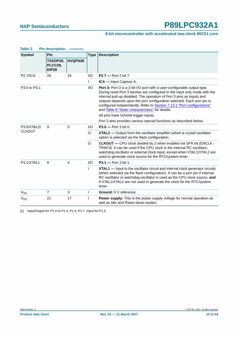
P2.7/ICA 28 24 I/O P2.7 — Port 2 bit 7.
I ICA — Input Capture A.
P3.0 to P3.1 I/O Port 3: Port 3 is a 2-bit I/O port with a user-configurable output type.During reset Port 3 latches are configured in the input only mode with theinternal pull-up disabled. The operation of Port 3 pins as inputs andoutputs depends upon the port configuration selected. Each port pin isconfigured independently. Refer to Section 7.13.1 “Port configurations”and Table 8 “Static characteristics” for details.
All pins have Schmitt trigger inputs.
Port 3 also provides various special functions as described below:
P3.0/XTAL2/CLKOUT
9 5 I/O P3.0 — Port 3 bit 0.
O XTAL2 — Output from the oscillator amplifier (when a crystal oscillatoroption is selected via the flash configuration.
O CLKOUT — CPU clock divided by 2 when enabled via SFR bit (ENCLK -TRIM.6). It can be used if the CPU clock is the internal RC oscillator,watchdog oscillator or external clock input, except when XTAL1/XTAL2 areused to generate clock source for the RTC/system timer.
P3.1/XTAL1 8 4 I/O P3.1 — Port 3 bit 1.
I XTAL1 — Input to the oscillator circuit and internal clock generator circuits(when selected via the flash configuration). It can be a port pin if internalRC oscillator or watchdog oscillator is used as the CPU clock source, andif XTAL1/XTAL2 are not used to generate the clock for the RTC/systemtimer.
VSS 7 3 I Ground: 0 V reference.
VDD 21 17 I Power supply: This is the power supply voltage for normal operation aswell as Idle and Power-down modes.
Table 2. Pin description …continued
Symbol Pin Type Description
TSSOP28,PLCC28,DIP28
HVQFN28
P89LPC932A1_3 © NXP B.V. 2007. All rights reserved.
Product data sheet Rev. 03 — 12 March 2007 10 of 64
NXP Semiconductors P89LPC932A18-bit microcontroller with accelerated two-clock 80C51 core
7. Functional description
Remark: Please refer to the P89LPC932A1 User manual for a more detailed functionaldescription.
7.1 Special function registersRemark: Special Function Registers (SFRs) accesses are restricted in the followingways:
• User must not attempt to access any SFR locations not defined.
• Accesses to any defined SFR locations must be strictly for the functions for the SFRs.
• SFR bits labeled ‘-’, logic 0 or logic 1 can only be written and read as follows:
– ‘-’ Unless otherwise specified, must be written with logic 0, but can return anyvalue when read (even if it was written with logic 0). It is a reserved bit and may beused in future derivatives.
– Logic 0 must be written with logic 0, and will return a logic 0 when read.
– Logic 1 must be written with logic 1, and will return a logic 1 when read.
P89LPC932A1_3 © NXP B.V. 2007. All rights reserved.
Product data sheet Rev. 03 — 12 March 2007 11 of 64
xxxxxxxxxxxxxxxxxxxxx xxxxxxxxxxxxxxxxxxxxxxxxxx xxxxxxx x x x xxxxxxxxxxxxxxxxxxxxxxxxxxxxxx xxxxxxxxxxxxxxxxxxx xx xxxxxxx xxxxxxxxxxxxxxxxxxxxxxxxxxx xxxxxxxxxxxxxxxxxxx xxxxxx xxxxxxxxxxxxxxxxxxxxxxxxxxxxxxxxxxx xxxxxxxxxxxx x xxxxxxxxxxxxxxxxxxxxxx xxxxxxxxxxxxxxxxxxxxxxxxxxxxxx xxxxx xxxxxxxxxxxxxxxxxxxxxxxxxxxxxxxxxxxxxxxxxxxxxxxxxx xxxxxxxxxxxxxxxxxxxxxxxxxxxxxxxxx xxxxxxxxxxxxxxxxxxxx xxx
P89LP
C932A
1_3
Product data shee
NX
P S
emiconductors
P89LP
C932A
18-bit m
icrocontroller with accelerated tw
o-clock 80C51 core
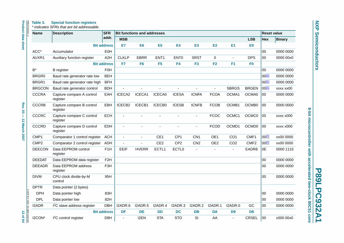
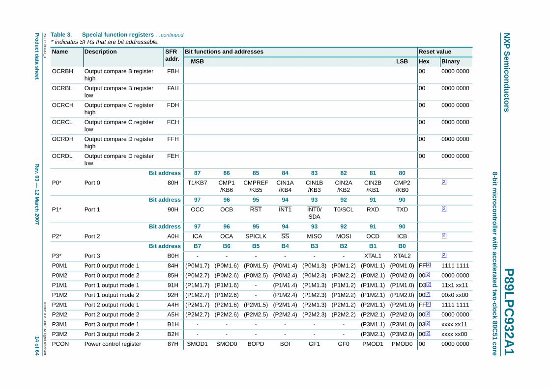
Table 3. Special function registers* indicates SFRs that are bit addressable.
Name Description SFRaddr.
Bit functions and addresses Reset value
MSB LSB Hex Binary
E1 E0
00 0000 0000
- DPS 00 0000 00x0
F1 F0
00 0000 0000
00[1] 0000 0000
00[1] 0000 0000
SBRGS BRGEN 00[1] xxxx xx00
OCMA1 OCMA0 00 0000 0000
OCMB1 OCMB0 00 0000 0000
OCMC1 OCMC0 00 xxxx x000
OCMD1 OCMD0 00 xxxx x000
CO1 CMF1 00[2] xx00 0000
CO2 CMF2 00[2] xx00 0000
- EADR8 0E 0000 1110
00 0000 0000
00 0000 0000
00 0000 0000
00 0000 0000
00 0000 0000
2ADR.0 GC 00 0000 0000
D9 D8
- CRSEL 00 x000 00x0
© N
XP
B.V. 2007. A
ll rights reserved.
tR
ev. 03 — 12 M
arch 200712 of 64
Bit address E7 E6 E5 E4 E3 E2
ACC* Accumulator E0H
AUXR1 Auxiliary function register A2H CLKLP EBRR ENT1 ENT0 SRST 0
Bit address F7 F6 F5 F4 F3 F2
B* B register F0H
BRGR0 Baud rate generator rate low BEH
BRGR1 Baud rate generator rate high BFH
BRGCON Baud rate generator control BDH - - - - - -
CCCRA Capture compare A controlregister
EAH ICECA2 ICECA1 ICECA0 ICESA ICNFA FCOA
CCCRB Capture compare B controlregister
EBH ICECB2 ICECB1 ICECB0 ICESB ICNFB FCOB
CCCRC Capture compare C controlregister
ECH - - - - - FCOC
CCCRD Capture compare D controlregister
EDH - - - - - FCOD
CMP1 Comparator 1 control register ACH - - CE1 CP1 CN1 OE1
CMP2 Comparator 2 control register ADH - - CE2 CP2 CN2 OE2
DEECON Data EEPROM controlregister
F1H EEIF HVERR ECTL1 ECTL0 - -
DEEDAT Data EEPROM data register F2H
DEEADR Data EEPROM addressregister
F3H
DIVM CPU clock divide-by-Mcontrol
95H
DPTR Data pointer (2 bytes)
DPH Data pointer high 83H
DPL Data pointer low 82H
I2ADR I2C slave address register DBH I2ADR.6 I2ADR.5 I2ADR.4 I2ADR.3 I2ADR.2 I2ADR.1 I
Bit address DF DE DD DC DB DA
I2CON* I2C control register D8H - I2EN STA STO SI AA
xxxxxxxxxxxxxxxxxxxxx xxxxxxxxxxxxxxxxxxxxxxxxxx xxxxxxx x x x xxxxxxxxxxxxxxxxxxxxxxxxxxxxxx xxxxxxxxxxxxxxxxxxx xx xxxxxxx xxxxxxxxxxxxxxxxxxxxxxxxxxx xxxxxxxxxxxxxxxxxxx xxxxxx xxxxxxxxxxxxxxxxxxxxxxxxxxxxxxxxxxx xxxxxxxxxxxx x xxxxxxxxxxxxxxxxxxxxxx xxxxxxxxxxxxxxxxxxxxxxxxxxxxxx xxxxx xxxxxxxxxxxxxxxxxxxxxxxxxxxxxxxxxxxxxxxxxxxxxxxxxx xxxxxxxxxxxxxxxxxxxxxxxxxxxxxxxxx xxxxxxxxxxxxxxxxxxxx xxx
P89LP
C932A
1_3
Product data shee
NX
P S
emiconductors
P89LP
C932A
18-bit m
icrocontroller with accelerated tw
o-clock 80C51 core
2
00 0000 0000
00 0000 0000
0 0 F8 1111 1000
00 0000 0000
00 0000 0000
00 0000 0000
00 0000 0000
A9 A8
ET0 EX0 00 0000 0000
E9 E8
EKBI EI2C 00[2] 00x0 0000
B9 B8
PT0 PX0 00[2] x000 0000
PT0H PX0H 00[2] x000 0000
F9 F8
PKBI PI2C 00[2] 00x0 0000
PKBIH PI2CH 00[2] 00x0 0000
PATN_SEL
KBIF 00[2] xxxx xx00
00 0000 0000
FF 1111 1111
00 0000 0000
00 0000 0000
Table 3. Special function registers …continued* indicates SFRs that are bit addressable.
Name Description SFRaddr.
Bit functions and addresses Reset value
MSB LSB Hex Binary
© N
XP
B.V. 2007. A
ll rights reserved.
tR
ev. 03 — 12 M
arch 200713 of 64
I2DAT I C data register DAH
I2SCLH Serial clock generator/SCLduty cycle register high
DDH
I2SCLL Serial clock generator/SCLduty cycle register low
DCH
I2STAT I2C status register D9H STA.4 STA.3 STA.2 STA.1 STA.0 0
ICRAH Input capture A register high ABH
ICRAL Input capture A register low AAH
ICRBH Input capture B register high AFH
ICRBL Input capture B register low AEH
Bit address AF AE AD AC AB AA
IEN0* Interrupt enable 0 A8H EA EWDRT EBO ES/ESR ET1 EX1
Bit address EF EE ED EC EB EA
IEN1* Interrupt enable 1 E8H EIEE EST - ECCU ESPI EC
Bit address BF BE BD BC BB BA
IP0* Interrupt priority 0 B8H - PWDRT PBO PS/PSR PT1 PX1
IP0H Interrupt priority 0 high B7H - PWDRTH
PBOH PSH/PSRH
PT1H PX1H
Bit address FF FE FD FC FB FA
IP1* Interrupt priority 1 F8H PIEE PST - PCCU PSPI PC
IP1H Interrupt priority 1 high F7H PIEEH PSTH - PCCUH PSPIH PCH
KBCON Keypad control register 94H - - - - - -
KBMASK Keypad interrupt maskregister
86H
KBPATN Keypad pattern register 93H
OCRAH Output compare A registerhigh
EFH
OCRAL Output compare A registerlow
EEH
xxxxxxxxxxxxxxxxxxxxx xxxxxxxxxxxxxxxxxxxxxxxxxx xxxxxxx x x x xxxxxxxxxxxxxxxxxxxxxxxxxxxxxx xxxxxxxxxxxxxxxxxxx xx xxxxxxx xxxxxxxxxxxxxxxxxxxxxxxxxxx xxxxxxxxxxxxxxxxxxx xxxxxx xxxxxxxxxxxxxxxxxxxxxxxxxxxxxxxxxxx xxxxxxxxxxxx x xxxxxxxxxxxxxxxxxxxxxx xxxxxxxxxxxxxxxxxxxxxxxxxxxxxx xxxxx xxxxxxxxxxxxxxxxxxxxxxxxxxxxxxxxxxxxxxxxxxxxxxxxxx xxxxxxxxxxxxxxxxxxxxxxxxxxxxxxxxx xxxxxxxxxxxxxxxxxxxx xxx
P89LP
C932A
1_3
Product data shee
NX
P S
emiconductors
P89LP
C932A
18-bit m
icrocontroller with accelerated tw
o-clock 80C51 core
00 0000 0000
00 0000 0000
00 0000 0000
00 0000 0000
00 0000 0000
00 0000 0000
81 80
CIN2B/KB1
CMP2/KB0
[2]
91 90
RXD TXD [2]
91 90
OCD ICB [2]
B1 B0
XTAL1 XTAL2 [2]
P0M1.1) (P0M1.0) FF[2] 1111 1111
P0M2.1) (P0M2.0) 00[2] 0000 0000
P1M1.1) (P1M1.0) D3[2] 11x1 xx11
P1M2.1) (P1M2.0) 00[2] 00x0 xx00
P2M1.1) (P2M1.0) FF[2] 1111 1111
P2M2.1) (P2M2.0) 00[2] 0000 0000
P3M1.1) (P3M1.0) 03[2] xxxx xx11
P3M2.1) (P3M2.0) 00[2] xxxx xx00
PMOD1 PMOD0 00 0000 0000
Table 3. Special function registers …continued* indicates SFRs that are bit addressable.
Name Description SFRaddr.
Bit functions and addresses Reset value
MSB LSB Hex Binary
© N
XP
B.V. 2007. A
ll rights reserved.
tR
ev. 03 — 12 M
arch 200714 of 64
OCRBH Output compare B registerhigh
FBH
OCRBL Output compare B registerlow
FAH
OCRCH Output compare C registerhigh
FDH
OCRCL Output compare C registerlow
FCH
OCRDH Output compare D registerhigh
FFH
OCRDL Output compare D registerlow
FEH
Bit address 87 86 85 84 83 82
P0* Port 0 80H T1/KB7 CMP1/KB6
CMPREF/KB5
CIN1A/KB4
CIN1B/KB3
CIN2A/KB2
Bit address 97 96 95 94 93 92
P1* Port 1 90H OCC OCB RST INT1 INT0/SDA
T0/SCL
Bit address 97 96 95 94 93 92
P2* Port 2 A0H ICA OCA SPICLK SS MISO MOSI
Bit address B7 B6 B5 B4 B3 B2
P3* Port 3 B0H - - - - - -
P0M1 Port 0 output mode 1 84H (P0M1.7) (P0M1.6) (P0M1.5) (P0M1.4) (P0M1.3) (P0M1.2) (
P0M2 Port 0 output mode 2 85H (P0M2.7) (P0M2.6) (P0M2.5) (P0M2.4) (P0M2.3) (P0M2.2) (
P1M1 Port 1 output mode 1 91H (P1M1.7) (P1M1.6) - (P1M1.4) (P1M1.3) (P1M1.2) (
P1M2 Port 1 output mode 2 92H (P1M2.7) (P1M2.6) - (P1M2.4) (P1M2.3) (P1M2.2) (
P2M1 Port 2 output mode 1 A4H (P2M1.7) (P2M1.6) (P2M1.5) (P2M1.4) (P2M1.3) (P2M1.2) (
P2M2 Port 2 output mode 2 A5H (P2M2.7) (P2M2.6) (P2M2.5) (P2M2.4) (P2M2.3) (P2M2.2) (
P3M1 Port 3 output mode 1 B1H - - - - - - (
P3M2 Port 3 output mode 2 B2H - - - - - - (
PCON Power control register 87H SMOD1 SMOD0 BOPD BOI GF1 GF0
xxxxxxxxxxxxxxxxxxxxx xxxxxxxxxxxxxxxxxxxxxxxxxx xxxxxxx x x x xxxxxxxxxxxxxxxxxxxxxxxxxxxxxx xxxxxxxxxxxxxxxxxxx xx xxxxxxx xxxxxxxxxxxxxxxxxxxxxxxxxxx xxxxxxxxxxxxxxxxxxx xxxxxx xxxxxxxxxxxxxxxxxxxxxxxxxxxxxxxxxxx xxxxxxxxxxxx x xxxxxxxxxxxxxxxxxxxxxx xxxxxxxxxxxxxxxxxxxxxxxxxxxxxx xxxxx xxxxxxxxxxxxxxxxxxxxxxxxxxxxxxxxxxxxxxxxxxxxxxxxxx xxxxxxxxxxxxxxxxxxxxxxxxxxxxxxxxx xxxxxxxxxxxxxxxxxxxx xxx
P89LP
C932A
1_3
Product data shee
NX
P S
emiconductors
P89LP
C932A
18-bit m
icrocontroller with accelerated tw
o-clock 80C51 core
SPD CCUPD 00[2] 0000 0000
D1 D0
F1 P 00 0000 0000
T0AD.1 - 00 xx00 000x
R_SF R_EX [3]
ERTC RTCEN 60[2][4] 011x xx00
00[4] 0000 0000
00[4] 0000 0000
00 0000 0000
00 0000 0000
xx xxxx xxxx
99 98
TI RI 00 0000 0000
OE STINT 00 0000 0000
07 0000 0111
SPR1 SPR0 04 0000 0100
- - 00 00xx xxxx
00 0000 0000
- T0M2 00 xxx0 xxx0
89 88
IE0 IT0 00 0000 0000
MOD21 TMOD20 00 0000 0000
LLDV.1 PLLDV.0 00 0xxx 0000
00 0000 0000
00 0000 0000
00 0000 0000
ICIE2B TICIE2A 00 0000 0x00
TICF2B TICF2A 00 0000 0x00
Table 3. Special function registers …continued* indicates SFRs that are bit addressable.
Name Description SFRaddr.
Bit functions and addresses Reset value
MSB LSB Hex Binary
© N
XP
B.V. 2007. A
ll rights reserved.
tR
ev. 03 — 12 M
arch 200715 of 64
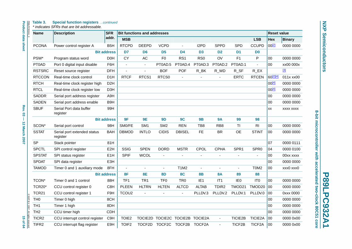
PCONA Power control register A B5H RTCPD DEEPD VCPD - I2PD SPPD
Bit address D7 D6 D5 D4 D3 D2
PSW* Program status word D0H CY AC F0 RS1 RS0 OV
PT0AD Port 0 digital input disable F6H - - PT0AD.5 PT0AD.4 PT0AD.3 PT0AD.2 P
RSTSRC Reset source register DFH - - BOF POF R_BK R_WD
RTCCON Real-time clock control D1H RTCF RTCS1 RTCS0 - - -
RTCH Real-time clock register high D2H
RTCL Real-time clock register low D3H
SADDR Serial port address register A9H
SADEN Serial port address enable B9H
SBUF Serial Port data bufferregister
99H
Bit address 9F 9E 9D 9C 9B 9A
SCON* Serial port control 98H SM0/FE SM1 SM2 REN TB8 RB8
SSTAT Serial port extended statusregister
BAH DBMOD INTLO CIDIS DBISEL FE BR
SP Stack pointer 81H
SPCTL SPI control register E2H SSIG SPEN DORD MSTR CPOL CPHA
SPSTAT SPI status register E1H SPIF WCOL - - - -
SPDAT SPI data register E3H
TAMOD Timer 0 and 1 auxiliary mode 8FH - - - T1M2 - -
Bit address 8F 8E 8D 8C 8B 8A
TCON* Timer 0 and 1 control 88H TF1 TR1 TF0 TR0 IE1 IT1
TCR20* CCU control register 0 C8H PLEEN HLTRN HLTEN ALTCD ALTAB TDIR2 T
TCR21 CCU control register 1 F9H TCOU2 - - - PLLDV.3 PLLDV.2 P
TH0 Timer 0 high 8CH
TH1 Timer 1 high 8DH
TH2 CCU timer high CDH
TICR2 CCU interrupt control register C9H TOIE2 TOCIE2D TOCIE2C TOCIE2B TOCIE2A - T
TIFR2 CCU interrupt flag register E9H TOIF2 TOCF2D TOCF2C TOCF2B TOCF2A -
xxxxxxxxxxxxxxxxxxxxx xxxxxxxxxxxxxxxxxxxxxxxxxx xxxxxxx x x x xxxxxxxxxxxxxxxxxxxxxxxxxxxxxx xxxxxxxxxxxxxxxxxxx xx xxxxxxx xxxxxxxxxxxxxxxxxxxxxxxxxxx xxxxxxxxxxxxxxxxxxx xxxxxx xxxxxxxxxxxxxxxxxxxxxxxxxxxxxxxxxxx xxxxxxxxxxxx x xxxxxxxxxxxxxxxxxxxxxx xxxxxxxxxxxxxxxxxxxxxxxxxxxxxx xxxxx xxxxxxxxxxxxxxxxxxxxxxxxxxxxxxxxxxxxxxxxxxxxxxxxxx xxxxxxxxxxxxxxxxxxxxxxxxxxxxxxxxx xxxxxxxxxxxxxxxxxxxx xxx
P89LP
C932A
1_3
Product data shee
NX
P S
emiconductors
P89LP
C932A
18-bit m
icrocontroller with accelerated tw
o-clock 80C51 core
npredictable.
ept POF and BOF; the power-on reset value is
TRIM register.
chdog reset and is logic 0 after power-on reset.
NCINT.1
ENCINT.0
00 xxxx x000
00 0000 0000
00 0000 0000
00 0000 0000
T0M1 T0M0 00 0000 0000
00 0000 0000
00 0000 0000
PCR2H.1
TPCR2H.0
00 xxxx xx00
PCR2L.1
TPCR2L.0
00 0000 0000
TRIM.1 TRIM.0 [5] [4]
WDTOF WDCLK [6] [4]
FF 1111 1111
Table 3. Special function registers …continued* indicates SFRs that are bit addressable.
Name Description SFRaddr.
Bit functions and addresses Reset value
MSB LSB Hex Binary
© N
XP
B.V. 2007. A
ll rights reserved.
tR
ev. 03 — 12 M
arch 200716 of 64
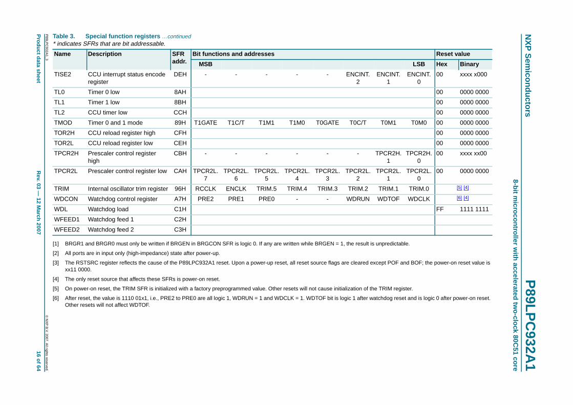
[1] BRGR1 and BRGR0 must only be written if BRGEN in BRGCON SFR is logic 0. If any are written while BRGEN = 1, the result is u
[2] All ports are in input only (high-impedance) state after power-up.
[3] The RSTSRC register reflects the cause of the P89LPC932A1 reset. Upon a power-up reset, all reset source flags are cleared excxx11 0000.
[4] The only reset source that affects these SFRs is power-on reset.
[5] On power-on reset, the TRIM SFR is initialized with a factory preprogrammed value. Other resets will not cause initialization of the
[6] After reset, the value is 1110 01x1, i.e., PRE2 to PRE0 are all logic 1, WDRUN = 1 and WDCLK = 1. WDTOF bit is logic 1 after watOther resets will not affect WDTOF.
TISE2 CCU interrupt status encoderegister
DEH - - - - - ENCINT.2
E
TL0 Timer 0 low 8AH
TL1 Timer 1 low 8BH
TL2 CCU timer low CCH
TMOD Timer 0 and 1 mode 89H T1GATE T1C/T T1M1 T1M0 T0GATE T0C/T
TOR2H CCU reload register high CFH
TOR2L CCU reload register low CEH
TPCR2H Prescaler control registerhigh
CBH - - - - - - T
TPCR2L Prescaler control register low CAH TPCR2L.7
TPCR2L.6
TPCR2L.5
TPCR2L.4
TPCR2L.3
TPCR2L.2
T
TRIM Internal oscillator trim register 96H RCCLK ENCLK TRIM.5 TRIM.4 TRIM.3 TRIM.2
WDCON Watchdog control register A7H PRE2 PRE1 PRE0 - - WDRUN
WDL Watchdog load C1H
WFEED1 Watchdog feed 1 C2H
WFEED2 Watchdog feed 2 C3H
NXP Semiconductors P89LPC932A18-bit microcontroller with accelerated two-clock 80C51 core
7.2 Enhanced CPUThe P89LPC932A1 uses an enhanced 80C51 CPU which runs at six times the speed ofstandard 80C51 devices. A machine cycle consists of two CPU clock cycles, and mostinstructions execute in one or two machine cycles.
7.3 Clocks
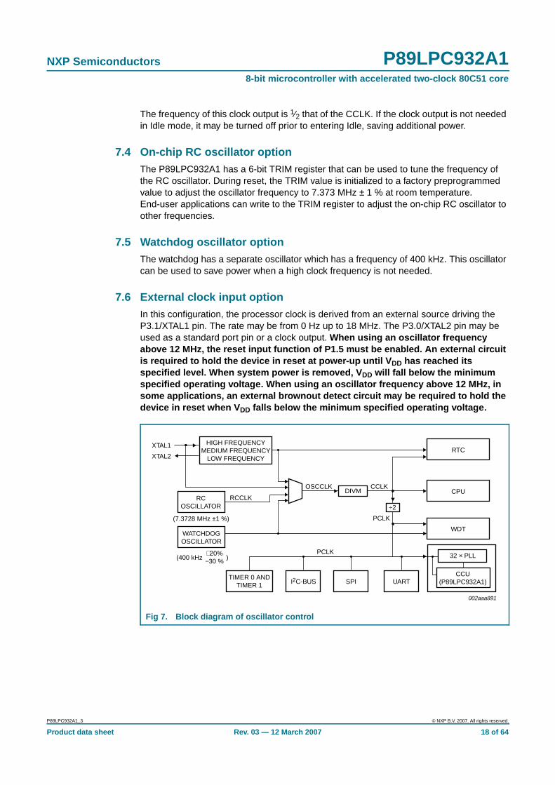
7.3.1 Clock definitions
The P89LPC932A1 device has several internal clocks as defined below:
OSCCLK — Input to the DIVM clock divider. OSCCLK is selected from one of four clocksources (see Figure 7) and can also be optionally divided to a slower frequency (seeSection 7.8 “CCLK modification: DIVM register”).
Note: fosc is defined as the OSCCLK frequency.
CCLK — CPU clock; output of the clock divider. There are two CCLK cycles per machinecycle, and most instructions are executed in one to two machine cycles (two or four CCLKcycles).
RCCLK — The internal 7.373 MHz RC oscillator output.
PCLK — Clock for the various peripheral devices and is CCLK⁄2.
7.3.2 CPU clock (OSCCLK)
The P89LPC932A1 provides several user-selectable oscillator options in generating theCPU clock. This allows optimization for a range of needs from high precision to lowestpossible cost. These options are configured when the flash is programmed and include anon-chip watchdog oscillator, an on-chip RC oscillator, an oscillator using an externalcrystal, or an external clock source. The crystal oscillator can be optimized for low,medium, or high frequency crystals covering a range from 20 kHz to 18 MHz.
7.3.3 Low speed oscillator option
This option supports an external crystal in the range of 20 kHz to 100 kHz. Ceramicresonators are also supported in this configuration.
7.3.4 Medium speed oscillator option
This option supports an external crystal in the range of 100 kHz to 4 MHz. Ceramicresonators are also supported in this configuration.
7.3.5 High speed oscillator option
This option supports an external crystal in the range of 4 MHz to 18 MHz. Ceramicresonators are also supported in this configuration.
7.3.6 Clock output
The P89LPC932A1 supports a user-selectable clock output function on theXTAL2/CLKOUT pin when crystal oscillator is not being used. This condition occurs ifanother clock source has been selected (on-chip RC oscillator, watchdog oscillator,external clock input on X1) and if the RTC is not using the crystal oscillator as its clocksource. This allows external devices to synchronize to the P89LPC932A1. This output isenabled by the ENCLK bit in the TRIM register.
P89LPC932A1_3 © NXP B.V. 2007. All rights reserved.
Product data sheet Rev. 03 — 12 March 2007 17 of 64
NXP Semiconductors P89LPC932A18-bit microcontroller with accelerated two-clock 80C51 core
The frequency of this clock output is 1⁄2 that of the CCLK. If the clock output is not neededin Idle mode, it may be turned off prior to entering Idle, saving additional power.
7.4 On-chip RC oscillator optionThe P89LPC932A1 has a 6-bit TRIM register that can be used to tune the frequency ofthe RC oscillator. During reset, the TRIM value is initialized to a factory preprogrammedvalue to adjust the oscillator frequency to 7.373 MHz ± 1 % at room temperature.End-user applications can write to the TRIM register to adjust the on-chip RC oscillator toother frequencies.
7.5 Watchdog oscillator optionThe watchdog has a separate oscillator which has a frequency of 400 kHz. This oscillatorcan be used to save power when a high clock frequency is not needed.
7.6 External clock input optionIn this configuration, the processor clock is derived from an external source driving theP3.1/XTAL1 pin. The rate may be from 0 Hz up to 18 MHz. The P3.0/XTAL2 pin may beused as a standard port pin or a clock output. When using an oscillator frequencyabove 12 MHz, the reset input function of P1.5 must be enabled. An external circuitis required to hold the device in reset at power-up until V DD has reached itsspecified level. When system power is removed, V DD will fall below the minimumspecified operating voltage. When using an oscillator frequency above 12 MHz, insome applications, an external brownout detect circuit may be required to hold thedevice in reset when V DD falls below the minimum specified operating voltage.
Fig 7. Block diagram of oscillator control
÷2
002aaa891
RTC
CPU
WDT
DIVMCCLK
UART
OSCCLK
I2C-BUS
PCLK
TIMER 0 ANDTIMER 1
HIGH FREQUENCYMEDIUM FREQUENCY
LOW FREQUENCY
XTAL1
XTAL2
RCOSCILLATOR
WATCHDOGOSCILLATOR
(7.3728 MHz ±1 %) PCLK
RCCLK
SPICCU
(P89LPC932A1)
32 × PLL+20%−30 %(400 kHz )
P89LPC932A1_3 © NXP B.V. 2007. All rights reserved.
Product data sheet Rev. 03 — 12 March 2007 18 of 64
NXP Semiconductors P89LPC932A18-bit microcontroller with accelerated two-clock 80C51 core
7.7 CCLK wake-up delayThe P89LPC932A1 has an internal wake-up timer that delays the clock until it stabilizesdepending on the clock source used. If the clock source is any of the three crystalselections (low, medium and high frequencies) the delay is 992 OSCCLK cycles plus60 µs to 100 µs. If the clock source is either the internal RC oscillator, watchdog oscillator,or external clock, the delay is 224 OSCCLK cycles plus 60 µs to 100 µs.
7.8 CCLK modification: DIVM registerThe OSCCLK frequency can be divided down up to 510 times by configuring a dividingregister, DIVM, to generate CCLK. This feature makes it possible to temporarily run theCPU at a lower rate, reducing power consumption. By dividing the clock, the CPU canretain the ability to respond to events that would not exit Idle mode by executing its normalprogram at a lower rate. This can also allow bypassing the oscillator start-up time in caseswhere Power-down mode would otherwise be used. The value of DIVM may be changedby the program at any time without interrupting code execution.
7.9 Low power selectThe P89LPC932A1 is designed to run at 12 MHz (CCLK) maximum. However, if CCLK is8 MHz or slower, the CLKLP SFR bit (AUXR1.7) can be set to logic 1 to lower the powerconsumption further. On any reset, CLKLP is logic 0 allowing highest performanceaccess. This bit can then be set in software if CCLK is running at 8 MHz or slower.
7.10 Memory organizationThe various P89LPC932A1 memory spaces are as follows:
• DATA
128 bytes of internal data memory space (00H:7FH) accessed via direct or indirectaddressing, using instructions other than MOVX and MOVC. All or part of the Stackmay be in this area.
• IDATA
Indirect Data. 256 bytes of internal data memory space (00H:FFH) accessed viaindirect addressing using instructions other than MOVX and MOVC. All or part of theStack may be in this area. This area includes the DATA area and the 128 bytesimmediately above it.
• SFR
Special Function Registers. Selected CPU registers and peripheral control and statusregisters, accessible only via direct addressing.
• XDATA
‘External’ Data or Auxiliary RAM. Duplicates the classic 80C51 64 kB memory spaceaddressed via the MOVX instruction using the SPTR, R0, or R1. All or part of thisspace could be implemented on-chip. The P89LPC932A1 has 512 bytes of on-chipXDATA memory.
P89LPC932A1_3 © NXP B.V. 2007. All rights reserved.
Product data sheet Rev. 03 — 12 March 2007 19 of 64
NXP Semiconductors P89LPC932A18-bit microcontroller with accelerated two-clock 80C51 core
• CODE
64 kB of Code memory space, accessed as part of program execution and via theMOVC instruction. The P89LPC932A1 has 8 kB of on-chip Code memory.
The P89LPC932A1 also has 512 bytes of on-chip Data EEPROM that is accessed viaSFRs (see Section 7.27 “Data EEPROM”).
7.11 Data RAM arrangementThe 768 bytes of on-chip RAM are organized as shown in Table 4.
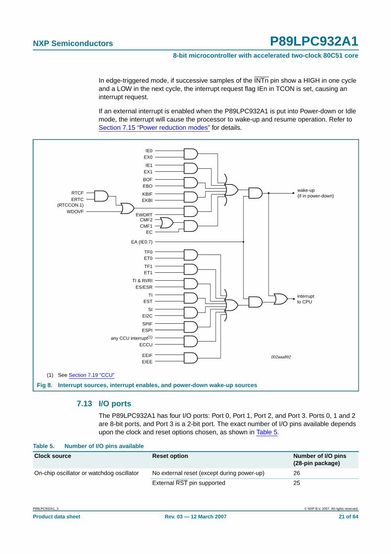
7.12 InterruptsThe P89LPC932A1 uses a four priority level interrupt structure. This allows great flexibilityin controlling the handling of the many interrupt sources. The P89LPC932A1 supports15 interrupt sources: external interrupts 0 and 1, timers 0 and 1, serial port Tx, serial portRx, combined serial port Rx/Tx, brownout detect, watchdog/RTC, I2C-bus, keyboard,comparators 1 and 2, SPI, CCU, and data EEPROM write completion.
Each interrupt source can be individually enabled or disabled by setting or clearing a bit inthe interrupt enable registers IEN0 or IEN1. The IEN0 register also contains a globaldisable bit, EA, which disables all interrupts.
Each interrupt source can be individually programmed to one of four priority levels bysetting or clearing bits in the interrupt priority registers IP0, IP0H, IP1, and IP1H. Aninterrupt service routine in progress can be interrupted by a higher priority interrupt, butnot by another interrupt of the same or lower priority. The highest priority interrupt servicecannot be interrupted by any other interrupt source. If two requests of different prioritylevels are pending at the start of an instruction, the request of higher priority level isserviced.
If requests of the same priority level are pending at the start of an instruction, an internalpolling sequence determines which request is serviced. This is called the arbitrationranking. Note that the arbitration ranking is only used to resolve pending requests of thesame priority level.
7.12.1 External interrupt inputs
The P89LPC932A1 has two external interrupt inputs as well as the Keypad Interruptfunction. The two interrupt inputs are identical to those present on the standard 80C51microcontrollers.
These external interrupts can be programmed to be level-triggered or edge-triggered bysetting or clearing bit IT1 or IT0 in Register TCON.
Table 4. On-chip data memory usages
Type Data RAM Size (bytes)
DATA Memory that can be addressed directly and indirectly 128
IDATA Memory that can be addressed indirectly 256
XDATA Auxiliary (‘External Data’) on-chip memory that is accessedusing the MOVX instructions
512
P89LPC932A1_3 © NXP B.V. 2007. All rights reserved.
Product data sheet Rev. 03 — 12 March 2007 20 of 64
NXP Semiconductors P89LPC932A18-bit microcontroller with accelerated two-clock 80C51 core
In edge-triggered mode, if successive samples of the INTn pin show a HIGH in one cycleand a LOW in the next cycle, the interrupt request flag IEn in TCON is set, causing aninterrupt request.
If an external interrupt is enabled when the P89LPC932A1 is put into Power-down or Idlemode, the interrupt will cause the processor to wake-up and resume operation. Refer toSection 7.15 “Power reduction modes” for details.
7.13 I/O portsThe P89LPC932A1 has four I/O ports: Port 0, Port 1, Port 2, and Port 3. Ports 0, 1 and 2are 8-bit ports, and Port 3 is a 2-bit port. The exact number of I/O pins available dependsupon the clock and reset options chosen, as shown in Table 5.
(1) See Section 7.19 “CCU”
Fig 8. Interrupt sources, interrupt enables, and power-down wake-up sources
002aaa892
IE0EX0
IE1EX1
BOFEBO
KBIFEKBI
interruptto CPU
wake-up(if in power-down)
EWDRTCMF2CMF1
EC
EA (IE0.7)
TF1ET1
TI & RI/RIES/ESR
TIEST
SIEI2C
SPIFESPI
RTCFERTC
(RTCCON.1)WDOVF
TF0ET0
any CCU interrupt(1)
ECCU
EIEEEEIF
Table 5. Number of I/O pins available
Clock source Reset option Number of I/O pins(28-pin package)
On-chip oscillator or watchdog oscillator No external reset (except during power-up) 26
External RST pin supported 25
P89LPC932A1_3 © NXP B.V. 2007. All rights reserved.
Product data sheet Rev. 03 — 12 March 2007 21 of 64

NXP Semiconductors P89LPC932A18-bit microcontroller with accelerated two-clock 80C51 core
[1] Required for operation above 12 MHz.
7.13.1 Port configurations
All but three I/O port pins on the P89LPC932A1 may be configured by software to one offour types on a bit-by-bit basis. These are: quasi-bidirectional (standard 80C51 portoutputs), push-pull, open drain, and input-only. Two configuration registers for each portselect the output type for each port pin.
1. P1.5 (RST) can only be an input and cannot be configured.
2. P1.2 (SCL/T0) and P1.3 (SDA/INT0) may only be configured to be either input-only oropen-drain.
7.13.1.1 Quasi-bidirectional output configuration
Quasi-bidirectional output type can be used as both an input and output without the needto reconfigure the port. This is possible because when the port outputs a logic HIGH, it isweakly driven, allowing an external device to pull the pin LOW. When the pin is drivenLOW, it is driven strongly and able to sink a fairly large current. These features aresomewhat similar to an open-drain output except that there are three pull-up transistors inthe quasi-bidirectional output that serve different purposes.
The P89LPC932A1 is a 3 V device, but the pins are 5 V-tolerant. In quasi-bidirectionalmode, if a user applies 5 V on the pin, there will be a current flowing from the pin to VDD,causing extra power consumption. Therefore, applying 5 V in quasi-bidirectional mode isdiscouraged.
A quasi-bidirectional port pin has a Schmitt trigger input that also has a glitch suppressioncircuit.
7.13.1.2 Open-drain output configuration
The open-drain output configuration turns off all pull-ups and only drives the pull-downtransistor of the port driver when the port latch contains a logic 0. To be used as a logicoutput, a port configured in this manner must have an external pull-up, typically a resistortied to VDD.
An open-drain port pin has a Schmitt trigger input that also has a glitch suppressioncircuit.
7.13.1.3 Input-only configuration
The input-only port configuration has no output drivers. It is a Schmitt trigger input thatalso has a glitch suppression circuit.
External clock input No external reset (except during power-up) 25
External RST pin supported[1] 24
Low/medium/high speed oscillator(external crystal or resonator)
No external reset (except during power-up) 24
External RST pin supported[1] 23
Table 5. Number of I/O pins available …continued
Clock source Reset option Number of I/O pins(28-pin package)
P89LPC932A1_3 © NXP B.V. 2007. All rights reserved.
Product data sheet Rev. 03 — 12 March 2007 22 of 64
NXP Semiconductors P89LPC932A18-bit microcontroller with accelerated two-clock 80C51 core
7.13.1.4 Push-pull output configuration
The push-pull output configuration has the same pull-down structure as both theopen-drain and the quasi-bidirectional output modes, but provides a continuous strongpull-up when the port latch contains a logic 1. The push-pull mode may be used whenmore source current is needed from a port output. A push-pull port pin has a Schmitttrigger input that also has a glitch suppression circuit.
7.13.2 Port 0 analog functions
The P89LPC932A1 incorporates two Analog Comparators. In order to give the bestanalog function performance and to minimize power consumption, pins that are beingused for analog functions must have the digital outputs and digital inputs disabled.
Digital outputs are disabled by putting the port output into the Input-only (high-impedance)mode.
Digital inputs on Port 0 may be disabled through the use of the PT0AD register, bits 1:5.On any reset, PT0AD[1:5] defaults to logic 0s to enable digital functions.
7.13.3 Additional port features
After power-up, all pins are in Input-only mode. Please note that this is different fromthe LPC76x series of devices.
• After power-up, all I/O pins except P1.5, may be configured by software.
• Pin P1.5 is input only. Pins P1.2 and P1.3 and are configurable for either input-only oropen-drain.
Every output on the P89LPC932A1 has been designed to sink typical LED drive current.However, there is a maximum total output current for all ports which must not beexceeded. Please refer to Table 8 “Static characteristics” for detailed specifications.
All ports pins that can function as an output have slew rate controlled outputs to limit noisegenerated by quickly switching output signals. The slew rate is factory-set toapproximately 10 ns rise and fall times.
7.14 Power monitoring functionsThe P89LPC932A1 incorporates power monitoring functions designed to preventincorrect operation during initial power-up and power loss or reduction during operation.This is accomplished with two hardware functions: Power-on detect and brownout detect.
7.14.1 Brownout detection
The brownout detect function determines if the power supply voltage drops below acertain level. The default operation is for a brownout detection to cause a processor reset,however it may alternatively be configured to generate an interrupt.
Brownout detection may be enabled or disabled in software.
If brownout detection is the brownout condition occurs when VDD falls below the brownouttrip voltage, Vbo (see Table 8 “Static characteristics”), and is negated when VDD risesabove Vbo. If the P89LPC932A1 device is to operate with a power supply that can bebelow 2.7 V, BOE should be left in the unprogrammed state so that the device can operateat 2.4 V, otherwise continuous brownout reset may prevent the device from operating.
P89LPC932A1_3 © NXP B.V. 2007. All rights reserved.
Product data sheet Rev. 03 — 12 March 2007 23 of 64
NXP Semiconductors P89LPC932A18-bit microcontroller with accelerated two-clock 80C51 core
For correct activation of brownout detect, the VDD rise and fall times must be observed.Please see Table 8 “Static characteristics” for specifications.
7.14.2 Power-on detection
The Power-on detect has a function similar to the brownout detect, but is designed to workas power comes up initially, before the power supply voltage reaches a level wherebrownout detect can work. The POF flag in the RSTSRC register is set to indicate aninitial power-up condition. The POF flag will remain set until cleared by software.
7.15 Power reduction modesThe P89LPC932A1 supports three different power reduction modes. These modes areIdle mode, Power-down mode, and Total Power-down mode.
7.15.1 Idle mode
Idle mode leaves peripherals running in order to allow them to activate the processorwhen an interrupt is generated. Any enabled interrupt source or reset may terminate Idlemode.
7.15.2 Power-down mode
The Power-down mode stops the oscillator in order to minimize power consumption. TheP89LPC932A1 exits Power-down mode via any reset, or certain interrupts. In Power-downmode, the power supply voltage may be reduced to the data retention voltage VDDR. Thisretains the RAM contents at the point where Power-down mode was entered. SFRcontents are not guaranteed after VDD has been lowered to VDDR, therefore it is highlyrecommended to wake up the processor via reset in this case. VDD must be raised towithin the operating range before the Power-down mode is exited.
Some chip functions continue to operate and draw power during Power-down mode,increasing the total power used during power-down. These include: Brownout detect,watchdog timer, Comparators (note that Comparators can be powered-down separately),and RTC/System Timer. The internal RC oscillator is disabled unless both the RCoscillator has been selected as the system clock and the RTC is enabled.
7.15.3 Total Power-down mode
This is the same as Power-down mode except that the brownout detection circuitry andthe voltage comparators are also disabled to conserve additional power. The internal RCoscillator is disabled unless both the RC oscillator has been selected as the system clockand the RTC is enabled. If the internal RC oscillator is used to clock the RTC duringpower-down, there will be high power consumption. Please use an external low frequencyclock to achieve low power with the RTC running during power-down.
7.16 ResetThe P1.5/RST pin can function as either an active-LOW reset input or as a digital input,P1.5. The RPE (Reset Pin Enable) bit in UCFG1, when set to logic 1, enables the externalreset input function on P1.5. When cleared, P1.5 may be used as an input pin.
Remark: During a power-up sequence, The RPE selection is overridden and this pin willalways functions as a reset input. An external circuit connected to this pin should nothold this pin LOW during a power-on sequence as this will keep the device in reset.
P89LPC932A1_3 © NXP B.V. 2007. All rights reserved.
Product data sheet Rev. 03 — 12 March 2007 24 of 64
NXP Semiconductors P89LPC932A18-bit microcontroller with accelerated two-clock 80C51 core
After power-up this input will function either as an external reset input or as a digital inputas defined by the RPE bit. Only a power-up reset will temporarily override the selectiondefined by RPE bit. Other sources of reset will not override the RPE bit.
Reset can be triggered from the following sources:
• External reset pin (during power-up or if user configured via UCFG1).
• Power-on detect.
• Brownout detect.
• Watchdog timer.
• Software reset.
• UART break character detect reset.
For every reset source, there is a flag in the Reset Register, RSTSRC. The user can readthis register to determine the most recent reset source. These flag bits can be cleared insoftware by writing a logic 0 to the corresponding bit. More than one flag bit may be set:
• During a power-on reset, both POF and BOF are set but the other flag bits arecleared.
• For any other reset, previously set flag bits that have not been cleared will remain set.
7.16.1 Reset vector
Following reset, the P89LPC932A1 will fetch instructions from either address 0000H orthe Boot address. The Boot address is formed by using the Boot Vector as the high byte ofthe address and the low byte of the address = 00H.
The Boot address will be used if a UART break reset occurs, or the non-volatile BootStatus bit (BOOTSTAT.0) = 1, or the device is forced into ISP mode during power-on (seeP89LPC932A1 User manual). Otherwise, instructions will be fetched from address 0000H.
7.17 Timers/counters 0 and 1The P89LPC932A1 has two general purpose counter/timers which are upward compatiblewith the standard 80C51 Timer 0 and Timer 1. Both can be configured to operate either astimers or event counter. An option to automatically toggle the T0 and/or T1 pins upon timeroverflow has been added.
In the ‘Timer’ function, the register is incremented every machine cycle.
In the ‘Counter’ function, the register is incremented in response to a 1-to-0 transition at itscorresponding external input pin, T0 or T1. In this function, the external input is sampledonce during every machine cycle.
Timer 0 and Timer 1 have five operating modes (modes 0, 1, 2, 3 and 6). Modes 0, 1, 2and 6 are the same for both Timers/Counters. Mode 3 is different.
7.17.1 Mode 0
Putting either Timer into Mode 0 makes it look like an 8048 Timer, which is an 8-bitCounter with a divide-by-32 prescaler. In this mode, the Timer register is configured as a13-bit register. Mode 0 operation is the same for Timer 0 and Timer 1.
P89LPC932A1_3 © NXP B.V. 2007. All rights reserved.
Product data sheet Rev. 03 — 12 March 2007 25 of 64
NXP Semiconductors P89LPC932A18-bit microcontroller with accelerated two-clock 80C51 core
7.17.2 Mode 1
Mode 1 is the same as Mode 0, except that all 16 bits of the timer register are used.
7.17.3 Mode 2
Mode 2 configures the Timer register as an 8-bit Counter with automatic reload. Mode 2operation is the same for Timer 0 and Timer 1.
7.17.4 Mode 3
When Timer 1 is in Mode 3 it is stopped. Timer 0 in Mode 3 forms two separate 8-bitcounters and is provided for applications that require an extra 8-bit timer. When Timer 1 isin Mode 3 it can still be used by the serial port as a baud rate generator.
7.17.5 Mode 6
In this mode, the corresponding timer can be changed to a PWM with a full period of256 timer clocks.
7.17.6 Timer overflow toggle output
Timers 0 and 1 can be configured to automatically toggle a port output whenever a timeroverflow occurs. The same device pins that are used for the T0 and T1 count inputs arealso used for the timer toggle outputs. The port outputs will be a logic 1 prior to the firsttimer overflow when this mode is turned on.
7.18 RTC/system timerThe P89LPC932A1 has a simple RTC that allows a user to continue running an accuratetimer while the rest of the device is powered-down. The RTC can be a wake-up or aninterrupt source. The RTC is a 23-bit down counter comprised of a 7-bit prescaler and a16-bit loadable down counter. When it reaches all logic 0s, the counter will be reloadedagain and the RTCF flag will be set. The clock source for this counter can be either theCCLK or the XTAL oscillator, provided that the XTAL oscillator is not being used as theCPU clock. If the XTAL oscillator is used as the CPU clock, then the RTC will use CCLK asits clock source. Only power-on reset will reset the RTC and its associated SFRs to thedefault state.
P89LPC932A1_3 © NXP B.V. 2007. All rights reserved.
Product data sheet Rev. 03 — 12 March 2007 26 of 64
NXP Semiconductors P89LPC932A18-bit microcontroller with accelerated two-clock 80C51 core
7.19 CCUThis unit features:
• A 16-bit timer with 16-bit reload on overflow.
• Selectable clock, with prescaler to divide clock source by any integral numberbetween 1 and 1024.
• Four Compare/PWM outputs with selectable polarity
• Symmetrical/Asymmetrical PWM selection
• Two Capture inputs with event counter and digital noise rejection filter
• Seven interrupts with common interrupt vector (one Overflow, two Capture,four Compare)
• Safe 16-bit read/write via shadow registers.
7.19.1 CCU clock
The CCU runs on the CCU Clock (CCUCLK), which is either PCLK in basic timer mode, orthe output of a Phase-Locked Loop (PLL). The PLL is designed to use a clock sourcebetween 0.5 MHz to 1 MHz that is multiplied by 32 to produce a CCUCLK between16 MHz and 32 MHz in PWM mode (asymmetrical or symmetrical). The PLL contains a4-bit divider to help divide PCLK into a frequency between 0.5 MHz and 1 MHz.
7.19.2 CCUCLK prescaling
This CCUCLK can further be divided down by a prescaler. The prescaler is implementedas a 10-bit free-running counter with programmable reload at overflow.
7.19.3 Basic timer operation
The Timer is a free-running up/down counter with a direction control bit. If the timercounting direction is changed while the counter is running, the count sequence will bereversed. The timer can be written or read at any time.
When a reload occurs, the CCU Timer Overflow Interrupt Flag will be set, and an interruptgenerated if enabled. The 16-bit CCU Timer may also be used as an 8-bit up/down timer.
7.19.4 Output compare
There are four output compare channels A, B, C and D. Each output compare channelneeds to be enabled in order to operate and the user will have to set the associated I/Opin to the desired output mode to connect the pin. When the contents of the timer matchesthat of a capture compare control register, the Timer Output Compare Interrupt Flag(TOCFx) becomes set. An interrupt will occur if enabled.
7.19.5 Input capture
Input capture is always enabled. Each time a capture event occurs on one of the two inputcapture pins, the contents of the timer is transferred to the corresponding 16-bit inputcapture register. The capture event can be programmed to be either rising or falling edgetriggered. A simple noise filter can be enabled on the input capture by enabling the InputCapture Noise Filter bit. If set, the capture logic needs to see four consecutive samples ofthe same value in order to recognize an edge as a capture event. An event counter can beset to delay a capture by a number of capture events.
P89LPC932A1_3 © NXP B.V. 2007. All rights reserved.
Product data sheet Rev. 03 — 12 March 2007 27 of 64
NXP Semiconductors P89LPC932A18-bit microcontroller with accelerated two-clock 80C51 core
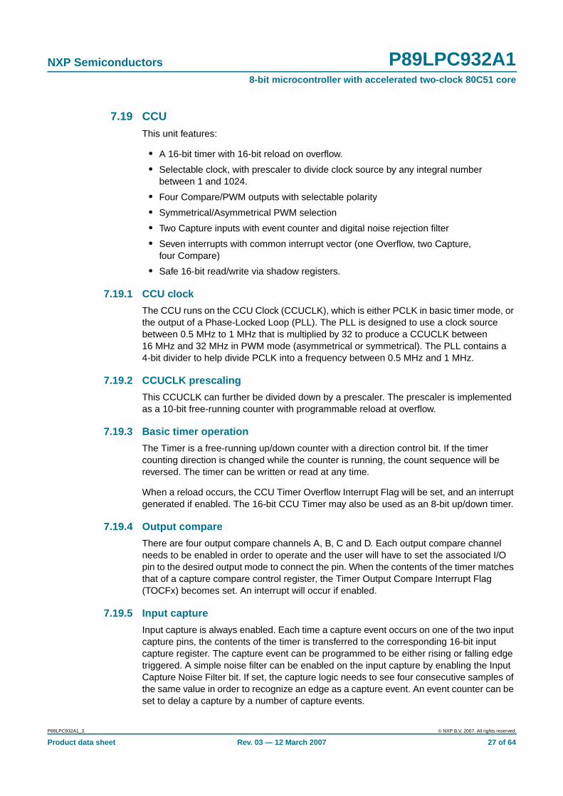
7.19.6 PWM operation
PWM operation has two main modes, symmetrical and asymmetrical.
In asymmetrical PWM operation the CCU Timer operates in down-counting moderegardless of the direction control bit.
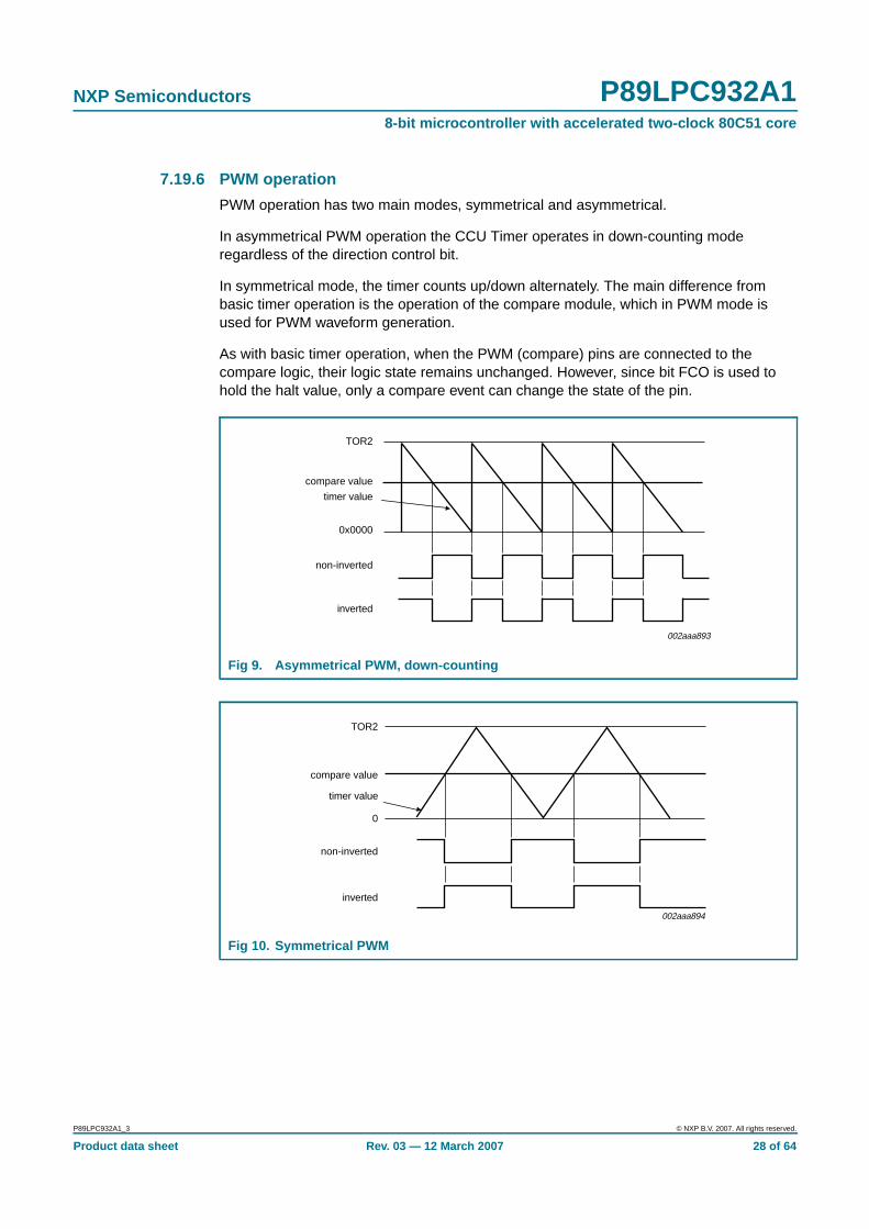
In symmetrical mode, the timer counts up/down alternately. The main difference frombasic timer operation is the operation of the compare module, which in PWM mode isused for PWM waveform generation.
As with basic timer operation, when the PWM (compare) pins are connected to thecompare logic, their logic state remains unchanged. However, since bit FCO is used tohold the halt value, only a compare event can change the state of the pin.
Fig 9. Asymmetrical PWM, down-counting
Fig 10. Symmetrical PWM
TOR2
compare value
timer value
non-inverted
inverted
0x0000
002aaa893
TOR2
compare value
timer value
non-inverted
inverted
002aaa894
0
P89LPC932A1_3 © NXP B.V. 2007. All rights reserved.
Product data sheet Rev. 03 — 12 March 2007 28 of 64
NXP Semiconductors P89LPC932A18-bit microcontroller with accelerated two-clock 80C51 core
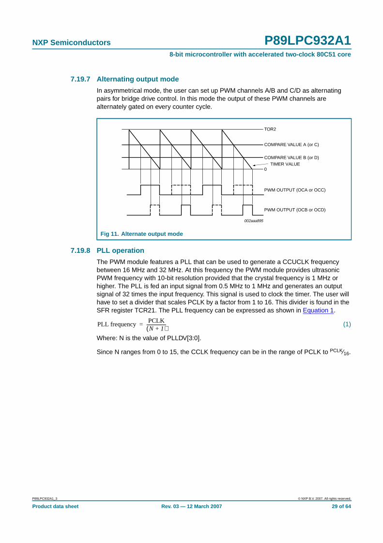
7.19.7 Alternating output mode
In asymmetrical mode, the user can set up PWM channels A/B and C/D as alternatingpairs for bridge drive control. In this mode the output of these PWM channels arealternately gated on every counter cycle.
7.19.8 PLL operation
The PWM module features a PLL that can be used to generate a CCUCLK frequencybetween 16 MHz and 32 MHz. At this frequency the PWM module provides ultrasonicPWM frequency with 10-bit resolution provided that the crystal frequency is 1 MHz orhigher. The PLL is fed an input signal from 0.5 MHz to 1 MHz and generates an outputsignal of 32 times the input frequency. This signal is used to clock the timer. The user willhave to set a divider that scales PCLK by a factor from 1 to 16. This divider is found in theSFR register TCR21. The PLL frequency can be expressed as shown in Equation 1.
(1)
Where: N is the value of PLLDV[3:0].
Since N ranges from 0 to 15, the CCLK frequency can be in the range of PCLK to PCLK⁄16.
Fig 11. Alternate output mode
TIMER VALUE
002aaa895
0
TOR2
COMPARE VALUE A (or C)
COMPARE VALUE B (or D)
PWM OUTPUT (OCA or OCC)
PWM OUTPUT (OCB or OCD)
PLL frequency PCLKN 1+( )------------------=
P89LPC932A1_3 © NXP B.V. 2007. All rights reserved.
Product data sheet Rev. 03 — 12 March 2007 29 of 64
NXP Semiconductors P89LPC932A18-bit microcontroller with accelerated two-clock 80C51 core
7.19.9 CCU interrupts
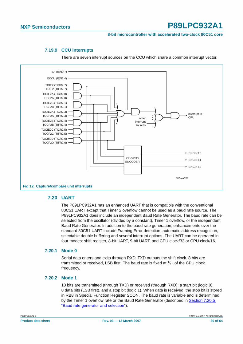
There are seven interrupt sources on the CCU which share a common interrupt vector.
7.20 UARTThe P89LPC932A1 has an enhanced UART that is compatible with the conventional80C51 UART except that Timer 2 overflow cannot be used as a baud rate source. TheP89LPC932A1 does include an independent Baud Rate Generator. The baud rate can beselected from the oscillator (divided by a constant), Timer 1 overflow, or the independentBaud Rate Generator. In addition to the baud rate generation, enhancements over thestandard 80C51 UART include Framing Error detection, automatic address recognition,selectable double buffering and several interrupt options. The UART can be operated infour modes: shift register, 8-bit UART, 9-bit UART, and CPU clock/32 or CPU clock/16.
7.20.1 Mode 0
Serial data enters and exits through RXD. TXD outputs the shift clock. 8 bits aretransmitted or received, LSB first. The baud rate is fixed at 1⁄16 of the CPU clockfrequency.
7.20.2 Mode 1
10 bits are transmitted (through TXD) or received (through RXD): a start bit (logic 0),8 data bits (LSB first), and a stop bit (logic 1). When data is received, the stop bit is storedin RB8 in Special Function Register SCON. The baud rate is variable and is determinedby the Timer 1 overflow rate or the Baud Rate Generator (described in Section 7.20.5“Baud rate generator and selection”).
Fig 12. Capture/compare unit interrupts
002aaa896
interrupt toCPU
TOIE2 (TICR2.7)TOIF2 (TIFR2.7)
TICIE2A (TICR2.0)TICF2A (TIFR2.0)
TICIE2B (TICR2.1)TICF2B (TIFR2.1)
TOCIE2A (TICR2.3)TOCF2A (TIFR2.3)
TOCIE2B (TICR2.4)TOCF2B (TIFR2.4)
TOCIE2C (TICR2.5)TOCF2C (TIFR2.5)
TOCIE2D (TICR2.6)TOCF2D (TIFR2.6)
EA (IEN0.7)
ECCU (IEN1.4)
PRIORITYENCODER
otherinterruptsources
ENCINT.0
ENCINT.1
ENCINT.2
P89LPC932A1_3 © NXP B.V. 2007. All rights reserved.
Product data sheet Rev. 03 — 12 March 2007 30 of 64
NXP Semiconductors P89LPC932A18-bit microcontroller with accelerated two-clock 80C51 core
7.20.3 Mode 2
11 bits are transmitted (through TXD) or received (through RXD): start bit (logic 0), 8 databits (LSB first), a programmable 9th data bit, and a stop bit (logic 1). When data istransmitted, the 9th data bit (TB8 in SCON) can be assigned the value of logic 0 or logic 1.Or, for example, the parity bit (P, in the PSW) could be moved into TB8. When data isreceived, the 9th data bit goes into RB8 in Special Function Register SCON, while the stopbit is not saved. The baud rate is programmable to either 1⁄16 or 1⁄32 of the CPU clockfrequency, as determined by the SMOD1 bit in PCON.
7.20.4 Mode 3
11 bits are transmitted (through TXD) or received (through RXD): a start bit (logic 0), 8data bits (LSB first), a programmable 9th data bit, and a stop bit (logic 1). In fact, Mode 3 isthe same as Mode 2 in all respects except baud rate. The baud rate in Mode 3 is variableand is determined by the Timer 1 overflow rate or the Baud Rate Generator (described inSection 7.20.5 “Baud rate generator and selection”).
7.20.5 Baud rate generator and selection
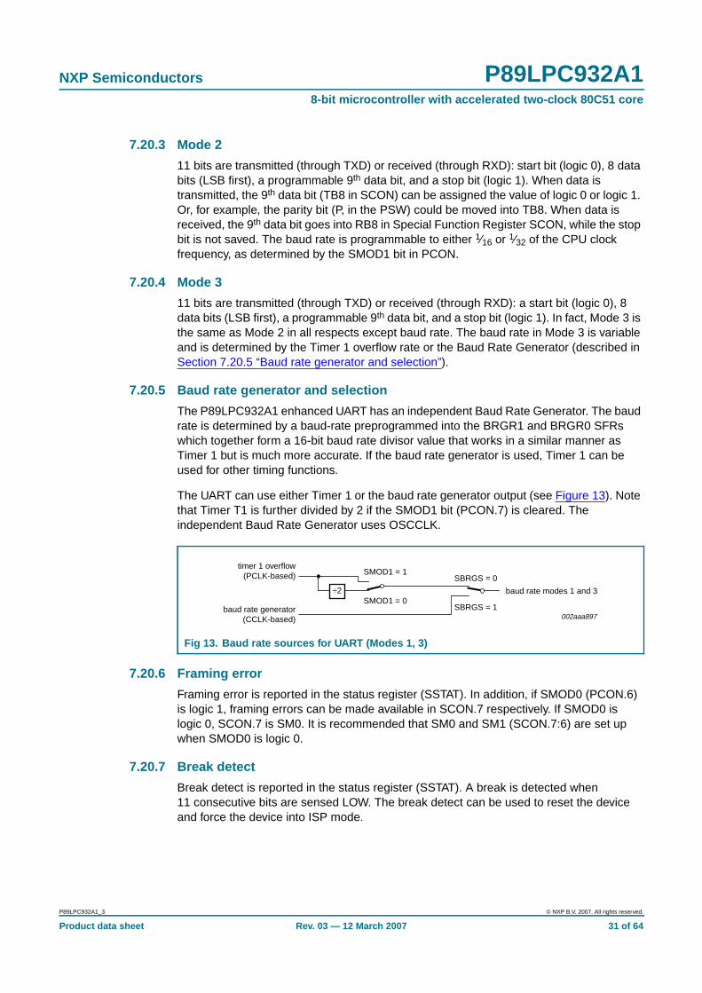
The P89LPC932A1 enhanced UART has an independent Baud Rate Generator. The baudrate is determined by a baud-rate preprogrammed into the BRGR1 and BRGR0 SFRswhich together form a 16-bit baud rate divisor value that works in a similar manner asTimer 1 but is much more accurate. If the baud rate generator is used, Timer 1 can beused for other timing functions.
The UART can use either Timer 1 or the baud rate generator output (see Figure 13). Notethat Timer T1 is further divided by 2 if the SMOD1 bit (PCON.7) is cleared. Theindependent Baud Rate Generator uses OSCCLK.
7.20.6 Framing error
Framing error is reported in the status register (SSTAT). In addition, if SMOD0 (PCON.6)is logic 1, framing errors can be made available in SCON.7 respectively. If SMOD0 islogic 0, SCON.7 is SM0. It is recommended that SM0 and SM1 (SCON.7:6) are set upwhen SMOD0 is logic 0.
7.20.7 Break detect
Break detect is reported in the status register (SSTAT). A break is detected when11 consecutive bits are sensed LOW. The break detect can be used to reset the deviceand force the device into ISP mode.
Fig 13. Baud rate sources for UART (Modes 1, 3)
baud rate modes 1 and 3
SBRGS = 1
SBRGS = 0
SMOD1 = 0
SMOD1 = 1timer 1 overflow
(PCLK-based)
baud rate generator(CCLK-based) 002aaa897
÷2
P89LPC932A1_3 © NXP B.V. 2007. All rights reserved.
Product data sheet Rev. 03 — 12 March 2007 31 of 64
NXP Semiconductors P89LPC932A18-bit microcontroller with accelerated two-clock 80C51 core
7.20.8 Double buffering
The UART has a transmit double buffer that allows buffering of the next character to bewritten to SBUF while the first character is being transmitted. Double buffering allowstransmission of a string of characters with only one stop bit between any two characters,as long as the next character is written between the start bit and the stop bit of theprevious character.
Double buffering can be disabled. If disabled (DBMOD, i.e., SSTAT.7 = 0), the UART iscompatible with the conventional 80C51 UART. If enabled, the UART allows writing toSnBUF while the previous data is being shifted out. Double buffering is only allowed inModes 1, 2 and 3. When operated in Mode 0, double buffering must be disabled(DBMOD = 0).
7.20.9 Transmit interrupts with double buffering enabled (modes 1, 2 and 3)
Unlike the conventional UART, in double buffering mode, the Tx interrupt is generatedwhen the double buffer is ready to receive new data.
7.20.10 The 9th bit (bit 8) in double buffering (modes 1, 2 and 3)
If double buffering is disabled TB8 can be written before or after SBUF is written, as longas TB8 is updated some time before that bit is shifted out. TB8 must not be changed untilthe bit is shifted out, as indicated by the Tx interrupt.
If double buffering is enabled, TB8 must be updated before SBUF is written, as TB8 willbe double-buffered together with SBUF data.
P89LPC932A1_3 © NXP B.V. 2007. All rights reserved.
Product data sheet Rev. 03 — 12 March 2007 32 of 64
NXP Semiconductors P89LPC932A18-bit microcontroller with accelerated two-clock 80C51 core
7.21 I2C-bus serial interfaceThe I2C-bus uses two wires (SDA and SCL) to transfer information between devicesconnected to the bus, and it has the following features:
• Bidirectional data transfer between masters and slaves.
• Multi master bus (no central master).
• Arbitration between simultaneously transmitting masters without corruption of serialdata on the bus.
• Serial clock synchronization allows devices with different bit rates to communicate viaone serial bus.
• Serial clock synchronization can be used as a handshake mechanism to suspend andresume serial transfer.
• The I2C-bus may be used for test and diagnostic purposes.
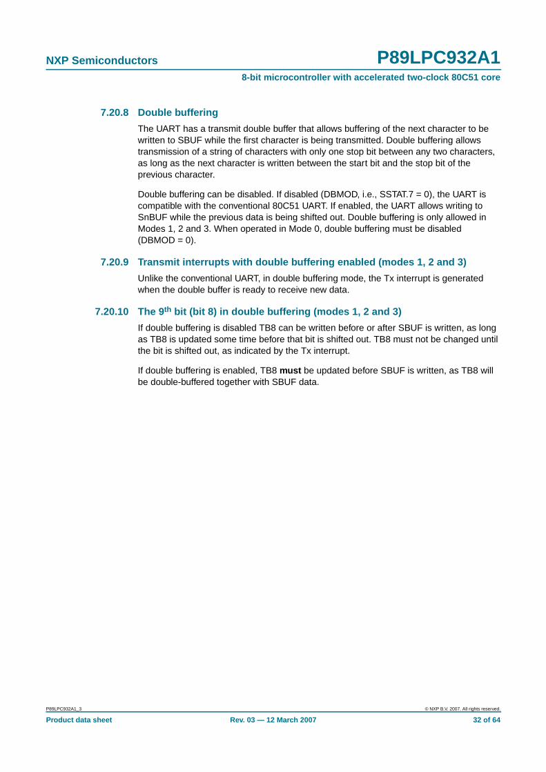
A typical I2C-bus configuration is shown in Figure 14. The P89LPC932A1 device providesa byte-oriented I2C-bus interface that supports data transfers up to 400 kHz.
Fig 14. I2C-bus configuration
OTHER DEVICEWITH I2C-BUS
INTERFACE
SDA
SCL
RPRP
OTHER DEVICEWITH I2C-BUS
INTERFACE
P1.3/SDA P1.2/SCL
P89LPC932A1
I2C-bus
002aaa898
P89LPC932A1_3 © NXP B.V. 2007. All rights reserved.
Product data sheet Rev. 03 — 12 March 2007 33 of 64
NXP Semiconductors P89LPC932A18-bit microcontroller with accelerated two-clock 80C51 core
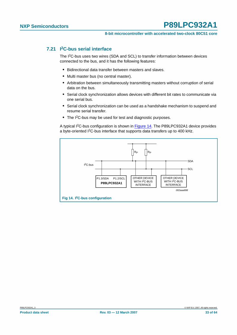
Fig 15. I2C-bus serial interface block diagram
INT
ER
NA
L B
US
002aaa899
ADDRESS REGISTER
COMPARATOR
SHIFT REGISTER
8
I2ADR
ACK
BIT COUNTER /ARBITRATION
AND SYNC LOGIC
8I2DAT
TIMINGAND
CONTROLLOGIC
SERIAL CLOCKGENERATOR
CCLK
interrupt
INPUTFILTER
OUTPUTSTAGE
INPUTFILTER
OUTPUTSTAGE
P1.3
P1.3/SDA
P1.2/SCL
P1.2
timer 1overflow
CONTROL REGISTERS ANDSCL DUTY CYCLE REGISTERS
I2CONI2SCLHI2SCLL
8
STATUSDECODERstatus bus
STATUS REGISTER
8
I2STAT
P89LPC932A1_3 © NXP B.V. 2007. All rights reserved.
Product data sheet Rev. 03 — 12 March 2007 34 of 64
NXP Semiconductors P89LPC932A18-bit microcontroller with accelerated two-clock 80C51 core
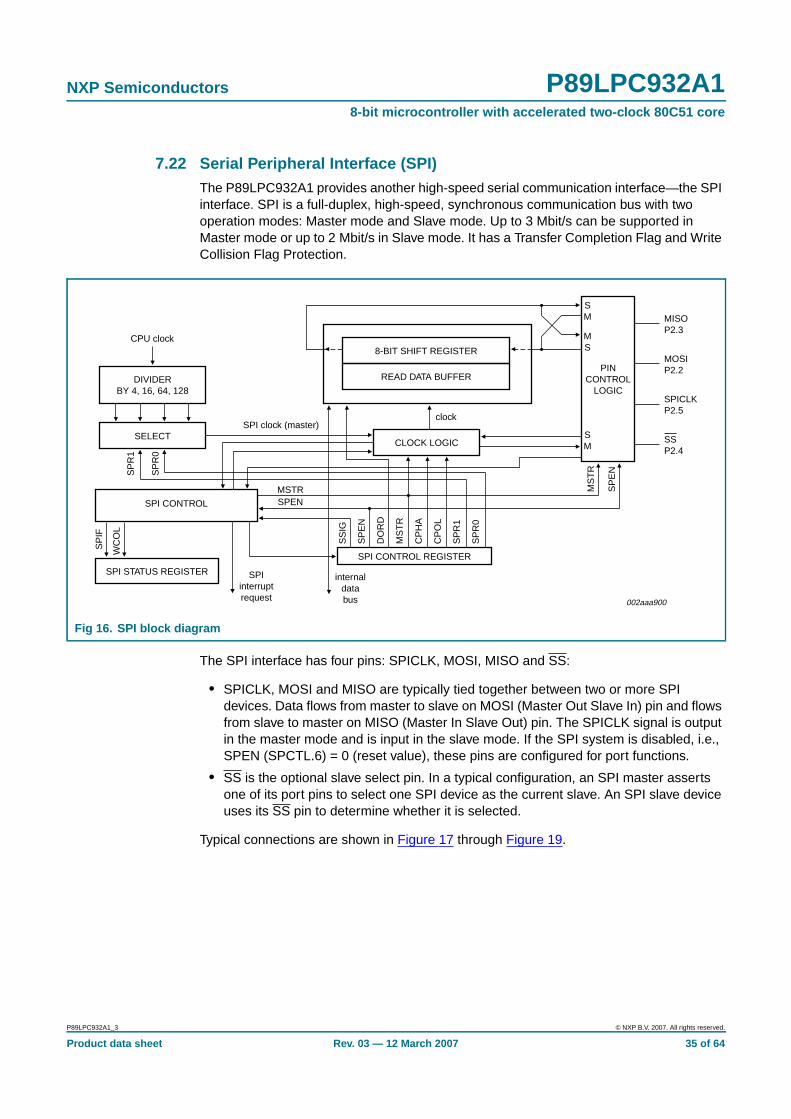
7.22 Serial Peripheral Interface (SPI)The P89LPC932A1 provides another high-speed serial communication interface—the SPIinterface. SPI is a full-duplex, high-speed, synchronous communication bus with twooperation modes: Master mode and Slave mode. Up to 3 Mbit/s can be supported inMaster mode or up to 2 Mbit/s in Slave mode. It has a Transfer Completion Flag and WriteCollision Flag Protection.
The SPI interface has four pins: SPICLK, MOSI, MISO and SS:
• SPICLK, MOSI and MISO are typically tied together between two or more SPIdevices. Data flows from master to slave on MOSI (Master Out Slave In) pin and flowsfrom slave to master on MISO (Master In Slave Out) pin. The SPICLK signal is outputin the master mode and is input in the slave mode. If the SPI system is disabled, i.e.,SPEN (SPCTL.6) = 0 (reset value), these pins are configured for port functions.
• SS is the optional slave select pin. In a typical configuration, an SPI master assertsone of its port pins to select one SPI device as the current slave. An SPI slave deviceuses its SS pin to determine whether it is selected.
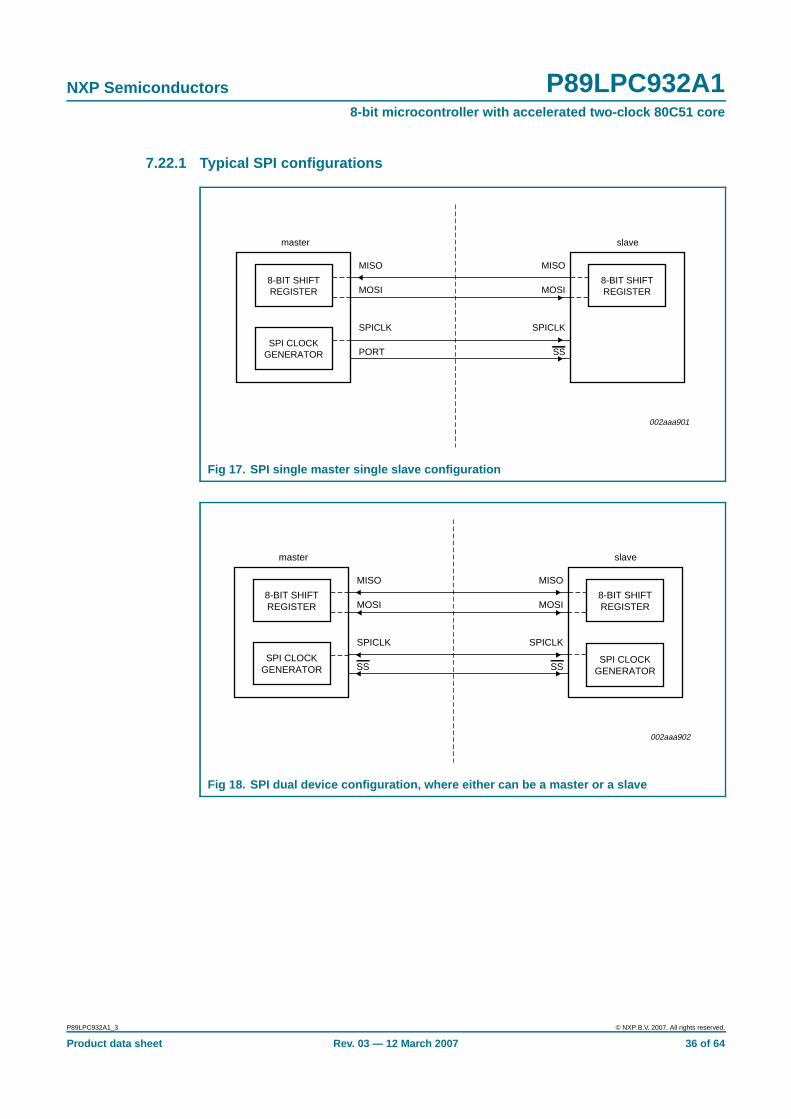
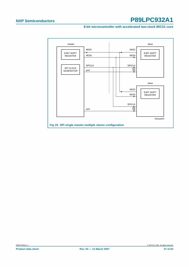
Typical connections are shown in Figure 17 through Figure 19.
Fig 16. SPI block diagram
002aaa900
CPU clock
DIVIDERBY 4, 16, 64, 128
SELECTCLOCK LOGIC
SPI CONTROL REGISTER
READ DATA BUFFER
8-BIT SHIFT REGISTER
SPI CONTROL
SPI STATUS REGISTER
SP
R1
SP
IF
WC
OL
SP
R0
SPI clock (master)
PINCONTROL
LOGIC
SM
SM
MS
MISOP2.3
MOSIP2.2
SPICLKP2.5
SSP2.4
SPIinterruptrequest
internaldatabus
SS
IG
SP
EN
SP
EN
MS
TR
DO
RD
MS
TR
CP
HA
CP
OL
SP
R1
SP
R0
MSTRSPEN
clock
P89LPC932A1_3 © NXP B.V. 2007. All rights reserved.
Product data sheet Rev. 03 — 12 March 2007 35 of 64
NXP Semiconductors P89LPC932A18-bit microcontroller with accelerated two-clock 80C51 core
7.22.1 Typical SPI configurations
Fig 17. SPI single master single slave configuration
Fig 18. SPI dual device configuration, where either can be a master or a slave
002aaa901
master slave
8-BIT SHIFTREGISTER
SPI CLOCKGENERATOR
8-BIT SHIFTREGISTER
MISO
MOSI
SPICLK
PORT
MISO
MOSI
SPICLK
SS
002aaa902
master slave
8-BIT SHIFTREGISTER
SPI CLOCKGENERATOR
SPI CLOCKGENERATOR
8-BIT SHIFTREGISTER
MISO
MOSI
SPICLK
MISO
MOSI
SPICLK
SSSS
P89LPC932A1_3 © NXP B.V. 2007. All rights reserved.
Product data sheet Rev. 03 — 12 March 2007 36 of 64
NXP Semiconductors P89LPC932A18-bit microcontroller with accelerated two-clock 80C51 core
Fig 19. SPI single master multiple slaves configuration
002aaa903
master slave
8-BIT SHIFTREGISTER
SPI CLOCKGENERATOR
8-BIT SHIFTREGISTER
MISO
MOSI
SPICLK
port
port
MISO
MOSI
SPICLK
SS
slave
8-BIT SHIFTREGISTER
MISO
MOSI
SPICLK
SS
P89LPC932A1_3 © NXP B.V. 2007. All rights reserved.
Product data sheet Rev. 03 — 12 March 2007 37 of 64
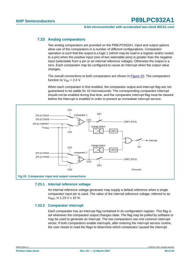
NXP Semiconductors P89LPC932A18-bit microcontroller with accelerated two-clock 80C51 core
7.23 Analog comparatorsTwo analog comparators are provided on the P89LPC932A1. Input and output optionsallow use of the comparators in a number of different configurations. Comparatoroperation is such that the output is a logic 1 (which may be read in a register and/or routedto a pin) when the positive input (one of two selectable pins) is greater than the negativeinput (selectable from a pin or an internal reference voltage). Otherwise the output is azero. Each comparator may be configured to cause an interrupt when the output valuechanges.
The overall connections to both comparators are shown in Figure 20. The comparatorsfunction to VDD = 2.4 V.
When each comparator is first enabled, the comparator output and interrupt flag are notguaranteed to be stable for 10 microseconds. The corresponding comparator interruptshould not be enabled during that time, and the comparator interrupt flag must be clearedbefore the interrupt is enabled in order to prevent an immediate interrupt service.
7.23.1 Internal reference voltage
An internal reference voltage generator may supply a default reference when a singlecomparator input pin is used. The value of the internal reference voltage, referred to asVREF, is 1.23 V ± 10 %.
7.23.2 Comparator interrupt
Each comparator has an interrupt flag contained in its configuration register. This flag isset whenever the comparator output changes state. The flag may be polled by software ormay be used to generate an interrupt. The two comparators use one common interruptvector. If both comparators enable interrupts, after entering the interrupt service routine,the user needs to read the flags to determine which comparator caused the interrupt.
Fig 20. Comparator input and output connections
comparator 1
CP1
CN1
(P0.4) CIN1A
(P0.3) CIN1B
(P0.5) CMPREF
Vref(bg)
OE1
change detect
CO1
CMF1
interrupt
002aaa904
CMP1 (P0.6)
ECchange detect
CMF2comparator 2
OE2
CO2CMP2 (P0.0)
CP2
CN2
(P0.2) CIN2A
(P0.1) CIN2B
P89LPC932A1_3 © NXP B.V. 2007. All rights reserved.
Product data sheet Rev. 03 — 12 March 2007 38 of 64
NXP Semiconductors P89LPC932A18-bit microcontroller with accelerated two-clock 80C51 core
7.23.3 Comparators and power reduction modes
Either or both comparators may remain enabled when Power-down or Idle mode isactivated, but both comparators are disabled automatically in Total Power-down mode.
If a comparator interrupt is enabled (except in Total Power-down mode), a change of thecomparator output state will generate an interrupt and wake up the processor. If thecomparator output to a pin is enabled, the pin should be configured in the push-pull modein order to obtain fast switching times while in Power-down mode. The reason is that withthe oscillator stopped, the temporary strong pull-up that normally occurs during switchingon a quasi-bidirectional port pin does not take place.
Comparators consume power in Power-down and Idle modes, as well as in the normaloperating mode. This fact should be taken into account when system power consumptionis an issue. To minimize power consumption, the user can disable the comparators viaPCONA.5, or put the device in Total Power-down mode.
7.24 Keypad interruptThe Keypad Interrupt function is intended primarily to allow a single interrupt to begenerated when Port 0 is equal to or not equal to a certain pattern. This function can beused for bus address recognition or keypad recognition. The user can configure the portvia SFRs for different tasks.
The Keypad Interrupt Mask Register (KBMASK) is used to define which input pinsconnected to Port 0 can trigger the interrupt. The Keypad Pattern Register (KBPATN) isused to define a pattern that is compared to the value of Port 0. The Keypad Interrupt Flag(KBIF) in the Keypad Interrupt Control Register (KBCON) is set when the condition ismatched while the Keypad Interrupt function is active. An interrupt will be generated ifenabled. The PATN_SEL bit in the Keypad Interrupt Control Register (KBCON) is used todefine equal or not-equal for the comparison.
In order to use the Keypad Interrupt as an original KBI function like in 87LPC76x series,the user needs to set KBPATN = 0FFH and PATN_SEL = 1 (not equal), then any keyconnected to Port 0 which is enabled by the KBMASK register will cause the hardware toset KBIF and generate an interrupt if it has been enabled. The interrupt may be used towake up the CPU from Idle or Power-down modes. This feature is particularly useful inhandheld, battery-powered systems that need to carefully manage power consumptionyet also need to be convenient to use.
In order to set the flag and cause an interrupt, the pattern on Port 0 must be held longerthan six CCLKs.
P89LPC932A1_3 © NXP B.V. 2007. All rights reserved.
Product data sheet Rev. 03 — 12 March 2007 39 of 64
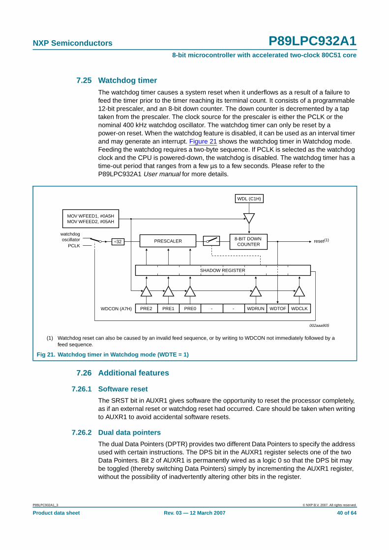
NXP Semiconductors P89LPC932A18-bit microcontroller with accelerated two-clock 80C51 core
7.25 Watchdog timerThe watchdog timer causes a system reset when it underflows as a result of a failure tofeed the timer prior to the timer reaching its terminal count. It consists of a programmable12-bit prescaler, and an 8-bit down counter. The down counter is decremented by a taptaken from the prescaler. The clock source for the prescaler is either the PCLK or thenominal 400 kHz watchdog oscillator. The watchdog timer can only be reset by apower-on reset. When the watchdog feature is disabled, it can be used as an interval timerand may generate an interrupt. Figure 21 shows the watchdog timer in Watchdog mode.Feeding the watchdog requires a two-byte sequence. If PCLK is selected as the watchdogclock and the CPU is powered-down, the watchdog is disabled. The watchdog timer has atime-out period that ranges from a few µs to a few seconds. Please refer to theP89LPC932A1 User manual for more details.
7.26 Additional features
7.26.1 Software reset
The SRST bit in AUXR1 gives software the opportunity to reset the processor completely,as if an external reset or watchdog reset had occurred. Care should be taken when writingto AUXR1 to avoid accidental software resets.
7.26.2 Dual data pointers
The dual Data Pointers (DPTR) provides two different Data Pointers to specify the addressused with certain instructions. The DPS bit in the AUXR1 register selects one of the twoData Pointers. Bit 2 of AUXR1 is permanently wired as a logic 0 so that the DPS bit maybe toggled (thereby switching Data Pointers) simply by incrementing the AUXR1 register,without the possibility of inadvertently altering other bits in the register.
(1) Watchdog reset can also be caused by an invalid feed sequence, or by writing to WDCON not immediately followed by afeed sequence.
Fig 21. Watchdog timer in Watchdog mode (WDTE = 1)
PRE2 PRE1 PRE0 - - WDRUN WDTOF WDCLKWDCON (A7H)
SHADOW REGISTER
PRESCALER
002aaa905
8-BIT DOWN COUNTER
WDL (C1H)
watchdogoscillator
PCLK÷32
MOV WFEED1, #0A5HMOV WFEED2, #05AH
reset(1)
P89LPC932A1_3 © NXP B.V. 2007. All rights reserved.
Product data sheet Rev. 03 — 12 March 2007 40 of 64

NXP Semiconductors P89LPC932A18-bit microcontroller with accelerated two-clock 80C51 core
7.27 Data EEPROMThe P89LPC932A1 has 512 B of on-chip data EEPROM. The data EEPROM is SFRbased, byte readable, byte writable, and erasable (via row fill and sector fill). The user canread, write and fill the memory via SFRs and one interrupt. This data EEPROM provides400000 minimum erase/program cycles for each byte.
• Byte mode: In this mode, data can be read and written one byte at a time.
• Row fill: In this mode, the addressed row (64 bytes) is filled with a single value. Theentire row can be erased by writing 00H.
• Sector fill: In this mode, all 512 bytes are filled with a single value. The entire sectorcan be erased by writing 00H.
After the operation finishes, the hardware will set the EEIF bit, which if enabled willgenerate an interrupt. The flag is cleared by software.
7.28 Flash program memory
7.28.1 General description
The P89LPC932A1 flash memory provides in-circuit electrical erasure and programming.The flash can be erased, read, and written as bytes. The Sector and Page Erase functionscan erase any flash sector (1 kB) or page (64 bytes). The Chip Erase operation will erasethe entire program memory. ICP using standard commercial programmers is available. Inaddition, IAP and byte-erase allows code memory to be used for non-volatile data storage.On-chip erase and write timing generation contribute to a user-friendly programminginterface. The P89LPC932A1 flash reliably stores memory contents even after400000 erase and program cycles. The cell is designed to optimize the erase andprogramming mechanisms. The P89LPC932A1 uses VDD as the supply voltage toperform the Program/Erase algorithms.
7.28.2 Features
• Programming and erase over the full operating voltage range.
• Byte erase allows code memory to be used for data storage.
• Read/Programming/Erase using ISP/IAP/ICP.
• Internal fixed boot ROM, containing low-level IAP routines available to user code.
• Default loader providing ISP via the serial port, located in upper end of user programmemory.
• Boot vector allows user-provided flash loader code to reside anywhere in the flashmemory space, providing flexibility to the user.
• Any flash program/erase operation in 2 ms.
• Programming with industry-standard commercial programmers.
• Programmable security for the code in the flash for each sector.
• 400000 typical erase/program cycles for each byte.
• 20 year minimum data retention.
P89LPC932A1_3 © NXP B.V. 2007. All rights reserved.
Product data sheet Rev. 03 — 12 March 2007 41 of 64
NXP Semiconductors P89LPC932A18-bit microcontroller with accelerated two-clock 80C51 core
7.28.3 Flash organization
The program memory consists of eight 1 kB sectors on the P89LPC932A1 device. Eachsector can be further divided into 64-byte pages. In addition to sector erase, page erase,and byte erase, a 64-byte page register is included which allows from 1 byte to 64 bytes ofa given page to be programmed at the same time, substantially reducing overallprogramming time.
7.28.4 Using flash as data storage
The flash code memory array of this device supports individual byte erasing andprogramming. Any byte in the code memory array may be read using the MOVCinstruction, provided that the sector containing the byte has not been secured (a MOVCinstruction is not allowed to read code memory contents of a secured sector). Thus anybyte in a non-secured sector may be used for non-volatile data storage.
7.28.5 Flash programming and erasing
Four different methods of erasing or programming of the flash are available. The flash maybe programmed or erased in the end-user application (IAP) under control of theapplication’s firmware. Another option is to use the ICP mechanism. This ICP systemprovides for programming through a serial clock - serial data interface. As shipped fromthe factory, the upper 512 bytes of user code space contains a serial ISP routine allowingfor the device to be programmed in circuit through the serial port. The flash may also beprogrammed or erased using a commercially available EPROM programmer whichsupports this device. This device does not provide for direct verification of code memorycontents. Instead, this device provides a 32-bit CRC result on either a sector or the entireuser code space.
7.28.6 In-circuit programming
ICP is performed without removing the microcontroller from the system. The ICP facilityconsists of internal hardware resources to facilitate remote programming of theP89LPC932A1 through a two-wire serial interface. The ICP facility has made ICP in anembedded application—using commercially available programmers—possible with aminimum of additional expense in components and circuit board area. The ICP functionuses five pins. Only a small connector needs to be available to interface your applicationto a commercial programmer in order to use this feature. Additional details may be foundin the P89LPC932A1 User manual.
7.28.7 In-application programming
IAP is performed in the application under the control of the microcontroller’s firmware. TheIAP facility consists of internal hardware resources to facilitate programming and erasing.The IAP facility has made IAP in an embedded application possible without additionalcomponents. Two methods are available to accomplish IAP. A set of predefined IAPfunctions are provided in a Boot ROM and can be called through a common interface,PGM_MTP. Several IAP calls are available for use by an application program to permitselective erasing and programming of flash sectors, pages, security bits, configurationbytes, and device ID. These functions are selected by setting up the microcontroller’sregisters before making a call to PGM_MTP at FF00H. The Boot ROM occupies theprogram memory space at the top of the address space from FF00H to FEFFH, therebynot conflicting with the user program memory space.
P89LPC932A1_3 © NXP B.V. 2007. All rights reserved.
Product data sheet Rev. 03 — 12 March 2007 42 of 64

NXP Semiconductors P89LPC932A18-bit microcontroller with accelerated two-clock 80C51 core
In addition, IAP operations can be accomplished through the use of four SFRs consistingof a control/status register, a data register, and two address registers. Additional detailsmay be found in the P89LPC932A1 User manual.
7.28.8 In-system programming
ISP is performed without removing the microcontroller from the system. The ISP facilityconsists of a series of internal hardware resources coupled with internal firmware tofacilitate remote programming of the P89LPC932A1 through the serial port. This firmwareis provided by NXP and embedded within each P89LPC932A1 device. The ISP facility hasmade ISP in an embedded application possible with a minimum of additional expense incomponents and circuit board area. The ISP function uses five pins (VDD, VSS, TXD, RXD,and RST). Only a small connector needs to be available to interface your application to anexternal circuit in order to use this feature.
7.28.9 Power-on reset code execution
The P89LPC932A1 contains two special flash elements: the Boot Vector and the BootStatus Bit. Following reset, the P89LPC932A1 examines the contents of the Boot StatusBit. If the Boot Status Bit is set to zero, power-up execution starts at location 0000H, whichis the normal start address of the user’s application code. When the Boot Status Bit is setto a value other than zero, the contents of the Boot Vector are used as the high byte of theexecution address and the low byte is set to 00H.
Table 6 shows the factory default Boot Vector settings for these devices. Note: Thesesettings are different than the original P89LPC932. Tools designed to support theP89LPC932A1 should be used to program this device, such as Flash Magic version1.98, or later. A factory-provided boot loader is preprogrammed into the address spaceindicated and uses the indicated boot loader entry point to perform ISP functions. Thiscode can be erased by the user. Users who wish to use this loader should takeprecautions to avoid erasing the 1 kB sector that contains this boot loader. Instead,the page erase function can be used to erase the first eight 64-byte pages located inthis sector. A custom boot loader can be written with the Boot Vector set to the customboot loader, if desired.
7.28.10 Hardware activation of the boot loader
The boot loader can also be executed by forcing the device into ISP mode during apower-on sequence (see the P89LPC932A1 User manual for specific information). Thishas the same effect as having a non-zero status byte. This allows an application to be builtthat will normally execute user code but can be manually forced into ISP operation. If thefactory default setting for the Boot Vector (1FH) is changed, it will no longer point to thefactory preprogrammed ISP boot loader code. After programming the flash, the statusbyte should be programmed to zero in order to allow execution of the user’s applicationcode beginning at address 0000H.
Table 6. Default Boot Vector values and ISP entry points
Device DefaultBoot Vector
Defaultboot loaderentry point
Default boot loadercode range
1 kB sectorrange
P89LPC932A1 1FH 1F00H 1E00H to 1FFFH 1C00H to 1FFFH
P89LPC932A1_3 © NXP B.V. 2007. All rights reserved.
Product data sheet Rev. 03 — 12 March 2007 43 of 64
NXP Semiconductors P89LPC932A18-bit microcontroller with accelerated two-clock 80C51 core
7.29 User configuration bytesSome user-configurable features of the P89LPC932A1 must be defined at power-up andtherefore cannot be set by the program after start of execution. These features areconfigured through the use of the flash byte UCFG1. Please see the P89LPC932A1 Usermanual for additional details.
7.30 User sector security bytesThere are eight User Sector Security Bytes on the P89LPC932A1 device. Each bytecorresponds to one sector. Please see the P89LPC932A1 User manual for additionaldetails.
P89LPC932A1_3 © NXP B.V. 2007. All rights reserved.
Product data sheet Rev. 03 — 12 March 2007 44 of 64
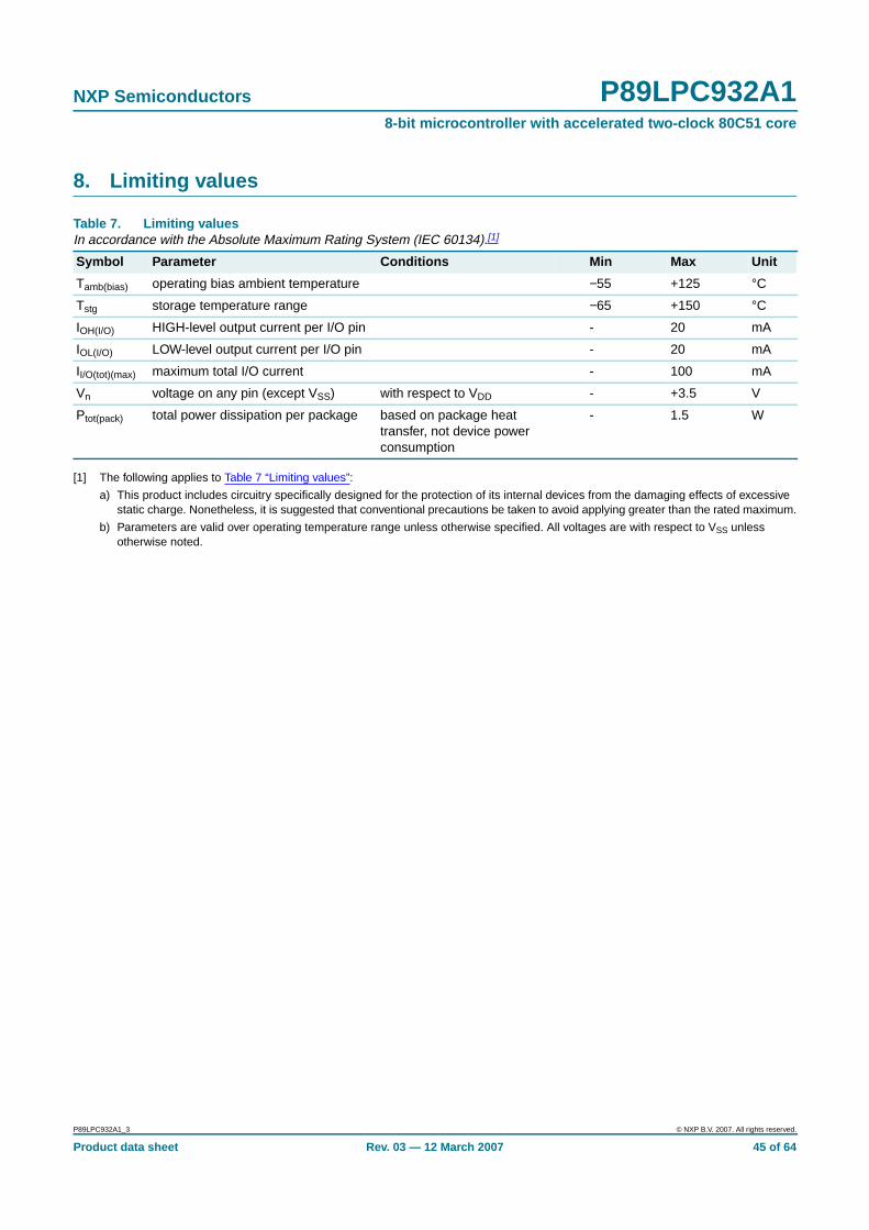
NXP Semiconductors P89LPC932A18-bit microcontroller with accelerated two-clock 80C51 core
8. Limiting values
[1] The following applies to Table 7 “Limiting values”:
a) This product includes circuitry specifically designed for the protection of its internal devices from the damaging effects of excessivestatic charge. Nonetheless, it is suggested that conventional precautions be taken to avoid applying greater than the rated maximum.
b) Parameters are valid over operating temperature range unless otherwise specified. All voltages are with respect to VSS unlessotherwise noted.
Table 7. Limiting valuesIn accordance with the Absolute Maximum Rating System (IEC 60134).[1]
Symbol Parameter Conditions Min Max Unit
Tamb(bias) operating bias ambient temperature −55 +125 °C
Tstg storage temperature range −65 +150 °C
IOH(I/O) HIGH-level output current per I/O pin - 20 mA
IOL(I/O) LOW-level output current per I/O pin - 20 mA
II/O(tot)(max) maximum total I/O current - 100 mA
Vn voltage on any pin (except VSS) with respect to VDD - +3.5 V
Ptot(pack) total power dissipation per package based on package heattransfer, not device powerconsumption
- 1.5 W
P89LPC932A1_3 © NXP B.V. 2007. All rights reserved.
Product data sheet Rev. 03 — 12 March 2007 45 of 64
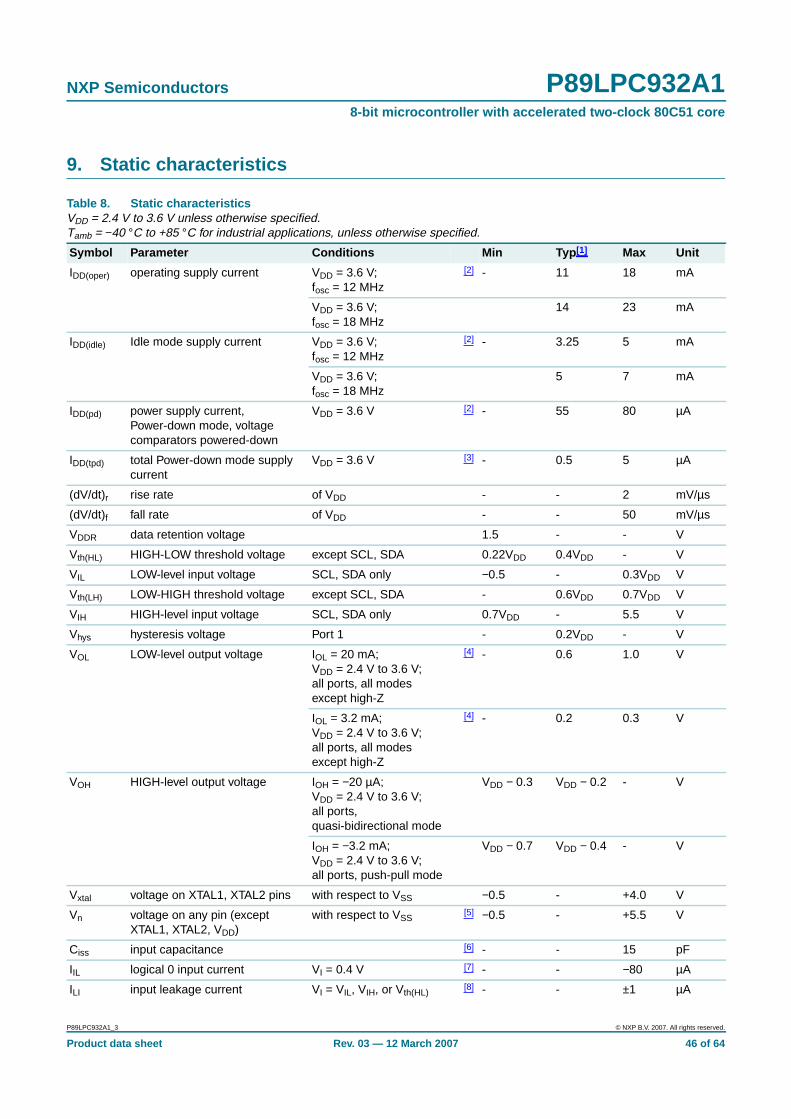
NXP Semiconductors P89LPC932A18-bit microcontroller with accelerated two-clock 80C51 core
9. Static characteristics
Table 8. Static characteristicsVDD = 2.4 V to 3.6 V unless otherwise specified.Tamb = −40 °C to +85 °C for industrial applications, unless otherwise specified.
Symbol Parameter Conditions Min Typ[1] Max Unit
IDD(oper) operating supply current VDD = 3.6 V;fosc = 12 MHz
[2] - 11 18 mA
VDD = 3.6 V;fosc = 18 MHz
14 23 mA
IDD(idle) Idle mode supply current VDD = 3.6 V;fosc = 12 MHz
[2] - 3.25 5 mA
VDD = 3.6 V;fosc = 18 MHz
5 7 mA
IDD(pd) power supply current,Power-down mode, voltagecomparators powered-down
VDD = 3.6 V [2] - 55 80 µA
IDD(tpd) total Power-down mode supplycurrent
VDD = 3.6 V [3] - 0.5 5 µA
(dV/dt)r rise rate of VDD - - 2 mV/µs
(dV/dt)f fall rate of VDD - - 50 mV/µs
VDDR data retention voltage 1.5 - - V
Vth(HL) HIGH-LOW threshold voltage except SCL, SDA 0.22VDD 0.4VDD - V
VIL LOW-level input voltage SCL, SDA only −0.5 - 0.3VDD V
Vth(LH) LOW-HIGH threshold voltage except SCL, SDA - 0.6VDD 0.7VDD V
VIH HIGH-level input voltage SCL, SDA only 0.7VDD - 5.5 V
Vhys hysteresis voltage Port 1 - 0.2VDD - V
VOL LOW-level output voltage IOL = 20 mA;VDD = 2.4 V to 3.6 V;all ports, all modesexcept high-Z
[4] - 0.6 1.0 V
IOL = 3.2 mA;VDD = 2.4 V to 3.6 V;all ports, all modesexcept high-Z
[4] - 0.2 0.3 V
VOH HIGH-level output voltage IOH = −20 µA;VDD = 2.4 V to 3.6 V;all ports,quasi-bidirectional mode
VDD − 0.3 VDD − 0.2 - V
IOH = −3.2 mA;VDD = 2.4 V to 3.6 V;all ports, push-pull mode
VDD − 0.7 VDD − 0.4 - V
Vxtal voltage on XTAL1, XTAL2 pins with respect to VSS −0.5 - +4.0 V
Vn voltage on any pin (exceptXTAL1, XTAL2, VDD)
with respect to VSS[5] −0.5 - +5.5 V
Ciss input capacitance [6] - - 15 pF
IIL logical 0 input current VI = 0.4 V [7] - - −80 µA
ILI input leakage current VI = VIL, VIH, or Vth(HL)[8] - - ±1 µA
P89LPC932A1_3 © NXP B.V. 2007. All rights reserved.
Product data sheet Rev. 03 — 12 March 2007 46 of 64
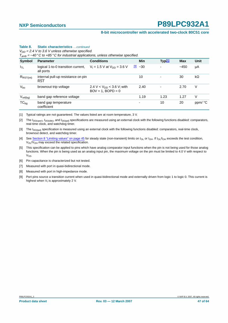
NXP Semiconductors P89LPC932A18-bit microcontroller with accelerated two-clock 80C51 core
[1] Typical ratings are not guaranteed. The values listed are at room temperature, 3 V.
[2] The IDD(oper), IDD(idle), and IDD(pd) specifications are measured using an external clock with the following functions disabled: comparators,real-time clock, and watchdog timer.
[3] The IDD(tpd) specification is measured using an external clock with the following functions disabled: comparators, real-time clock,brownout detect, and watchdog timer.
[4] See Section 8 “Limiting values” on page 45 for steady state (non-transient) limits on IOL or IOH. If IOL/IOH exceeds the test condition,VOL/VOH may exceed the related specification.
[5] This specification can be applied to pins which have analog comparator input functions when the pin is not being used for those analogfunctions. When the pin is being used as an analog input pin, the maximum voltage on the pin must be limited to 4.0 V with respect toVSS.
[6] Pin capacitance is characterized but not tested.
[7] Measured with port in quasi-bidirectional mode.
[8] Measured with port in high-impedance mode.
[9] Port pins source a transition current when used in quasi-bidirectional mode and externally driven from logic 1 to logic 0. This current ishighest when VI is approximately 2 V.
ITL logical 1-to-0 transition current,all ports
VI = 1.5 V at VDD = 3.6 V [9] −30 - −450 µA
RRST(int) internal pull-up resistance on pinRST
10 - 30 kΩ
Vbo brownout trip voltage 2.4 V < VDD < 3.6 V; withBOV = 1, BOPD = 0
2.40 - 2.70 V
Vref(bg) band gap reference voltage 1.19 1.23 1.27 V
TCbg band gap temperaturecoefficient
- 10 20 ppm/ °C
Table 8. Static characteristics …continuedVDD = 2.4 V to 3.6 V unless otherwise specified.Tamb = −40 °C to +85 °C for industrial applications, unless otherwise specified.
Symbol Parameter Conditions Min Typ[1] Max Unit
P89LPC932A1_3 © NXP B.V. 2007. All rights reserved.
Product data sheet Rev. 03 — 12 March 2007 47 of 64
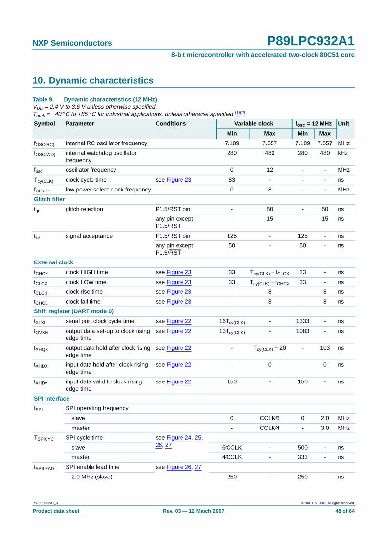
NXP Semiconductors P89LPC932A18-bit microcontroller with accelerated two-clock 80C51 core
10. Dynamic characteristics
Table 9. Dynamic characteristics (12 MHz)VDD = 2.4 V to 3.6 V unless otherwise specified.Tamb = −40 °C to +85 °C for industrial applications, unless otherwise specified.[1][2]
Symbol Parameter Conditions Variable clock fosc = 12 MHz Unit
Min Max Min Max
fOSC(RC) internal RC oscillator frequency 7.189 7.557 7.189 7.557 MHz
fOSC(WD) internal watchdog oscillatorfrequency
280 480 280 480 kHz
fosc oscillator frequency 0 12 - - MHz
Tcy(CLK) clock cycle time see Figure 23 83 - - - ns
fCLKLP low power select clock frequency 0 8 - - MHz
Glitch filter
tgr glitch rejection P1.5/RST pin - 50 - 50 ns
any pin exceptP1.5/RST
- 15 - 15 ns
tsa signal acceptance P1.5/RST pin 125 - 125 - ns
any pin exceptP1.5/RST
50 - 50 - ns
External clock
tCHCX clock HIGH time see Figure 23 33 Tcy(CLK) − tCLCX 33 - ns
tCLCX clock LOW time see Figure 23 33 Tcy(CLK) − tCHCX 33 - ns
tCLCH clock rise time see Figure 23 - 8 - 8 ns
tCHCL clock fall time see Figure 23 - 8 - 8 ns
Shift register (UART mode 0)
tXLXL serial port clock cycle time see Figure 22 16Tcy(CLK) - 1333 - ns
tQVXH output data set-up to clock risingedge time
see Figure 22 13Tcy(CLK) - 1083 - ns
tXHQX output data hold after clock risingedge time
see Figure 22 - Tcy(CLK) + 20 - 103 ns
tXHDX input data hold after clock risingedge time
see Figure 22 - 0 - 0 ns
tXHDV input data valid to clock risingedge time
see Figure 22 150 - 150 - ns
SPI interface
fSPI SPI operating frequency
slave 0 CCLK⁄6 0 2.0 MHz
master - CCLK⁄4 - 3.0 MHz
TSPICYC SPI cycle time see Figure 24, 25,26, 27slave 6⁄CCLK - 500 - ns
master 4⁄CCLK - 333 - ns
tSPILEAD SPI enable lead time see Figure 26, 27
2.0 MHz (slave) 250 - 250 - ns
P89LPC932A1_3 © NXP B.V. 2007. All rights reserved.
Product data sheet Rev. 03 — 12 March 2007 48 of 64
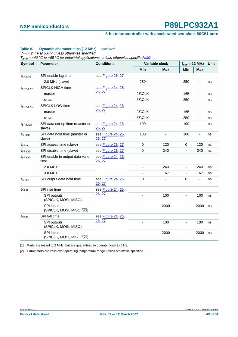
NXP Semiconductors P89LPC932A18-bit microcontroller with accelerated two-clock 80C51 core
[1] Parts are tested to 2 MHz, but are guaranteed to operate down to 0 Hz.
[2] Parameters are valid over operating temperature range unless otherwise specified.
tSPILAG SPI enable lag time see Figure 26, 27
2.0 MHz (slave) 250 - 250 - ns
tSPICLKH SPICLK HIGH time see Figure 24, 25,26, 27master 2⁄CCLK - 165 - ns
slave 3⁄CCLK - 250 - ns
tSPICLKL SPICLK LOW time see Figure 24, 25,26, 27master 2⁄CCLK - 165 - ns
slave 3⁄CCLK - 250 - ns
tSPIDSU SPI data set-up time (master orslave)
see Figure 24, 25,26, 27
100 - 100 - ns
tSPIDH SPI data hold time (master orslave)
see Figure 24, 25,26, 27
100 - 100 - ns
tSPIA SPI access time (slave) see Figure 26, 27 0 120 0 120 ns
tSPIDIS SPI disable time (slave) see Figure 26, 27 0 240 - 240 ns
tSPIDV SPI enable to output data validtime
see Figure 24, 25,26, 27
2.0 MHz - 240 - 240 ns
3.0 MHz - 167 - 167 ns
tSPIOH SPI output data hold time see Figure 24, 25,26, 27
0 - 0 - ns
tSPIR SPI rise time see Figure 24, 25,26, 27SPI outputs
(SPICLK, MOSI, MISO)- 100 - 100 ns
SPI inputs(SPICLK, MOSI, MISO, SS)
- 2000 - 2000 ns
tSPIF SPI fall time see Figure 24, 25,26, 27SPI outputs
(SPICLK, MOSI, MISO)- 100 - 100 ns
SPI inputs(SPICLK, MOSI, MISO, SS)
- 2000 - 2000 ns
Table 9. Dynamic characteristics (12 MHz) …continuedVDD = 2.4 V to 3.6 V unless otherwise specified.Tamb = −40 °C to +85 °C for industrial applications, unless otherwise specified.[1][2]
Symbol Parameter Conditions Variable clock fosc = 12 MHz Unit
Min Max Min Max
P89LPC932A1_3 © NXP B.V. 2007. All rights reserved.
Product data sheet Rev. 03 — 12 March 2007 49 of 64
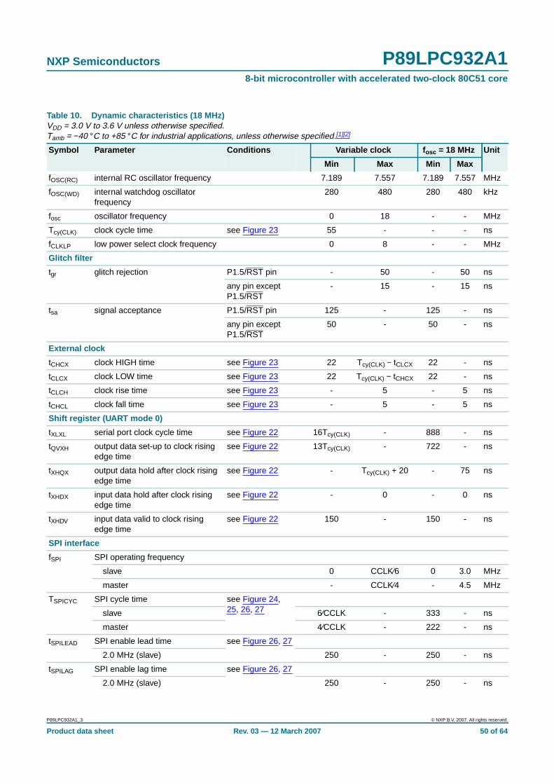
NXP Semiconductors P89LPC932A18-bit microcontroller with accelerated two-clock 80C51 core
Table 10. Dynamic characteristics (18 MHz)VDD = 3.0 V to 3.6 V unless otherwise specified.Tamb = −40 °C to +85 °C for industrial applications, unless otherwise specified.[1][2]
Symbol Parameter Conditions Variable clock fosc = 18 MHz Unit
Min Max Min Max
fOSC(RC) internal RC oscillator frequency 7.189 7.557 7.189 7.557 MHz
fOSC(WD) internal watchdog oscillatorfrequency
280 480 280 480 kHz
fosc oscillator frequency 0 18 - - MHz
Tcy(CLK) clock cycle time see Figure 23 55 - - - ns
fCLKLP low power select clock frequency 0 8 - - MHz
Glitch filter
tgr glitch rejection P1.5/RST pin - 50 - 50 ns
any pin exceptP1.5/RST
- 15 - 15 ns
tsa signal acceptance P1.5/RST pin 125 - 125 - ns
any pin exceptP1.5/RST
50 - 50 - ns
External clock
tCHCX clock HIGH time see Figure 23 22 Tcy(CLK) − tCLCX 22 - ns
tCLCX clock LOW time see Figure 23 22 Tcy(CLK) − tCHCX 22 - ns
tCLCH clock rise time see Figure 23 - 5 - 5 ns
tCHCL clock fall time see Figure 23 - 5 - 5 ns
Shift register (UART mode 0)
tXLXL serial port clock cycle time see Figure 22 16Tcy(CLK) - 888 - ns
tQVXH output data set-up to clock risingedge time
see Figure 22 13Tcy(CLK) - 722 - ns
tXHQX output data hold after clock risingedge time
see Figure 22 - Tcy(CLK) + 20 - 75 ns
tXHDX input data hold after clock risingedge time
see Figure 22 - 0 - 0 ns
tXHDV input data valid to clock risingedge time
see Figure 22 150 - 150 - ns
SPI interface
fSPI SPI operating frequency
slave 0 CCLK⁄6 0 3.0 MHz
master - CCLK⁄4 - 4.5 MHz
TSPICYC SPI cycle time see Figure 24,25, 26, 27slave 6⁄CCLK - 333 - ns
master 4⁄CCLK - 222 - ns
tSPILEAD SPI enable lead time see Figure 26, 27
2.0 MHz (slave) 250 - 250 - ns
tSPILAG SPI enable lag time see Figure 26, 27
2.0 MHz (slave) 250 - 250 - ns
P89LPC932A1_3 © NXP B.V. 2007. All rights reserved.
Product data sheet Rev. 03 — 12 March 2007 50 of 64
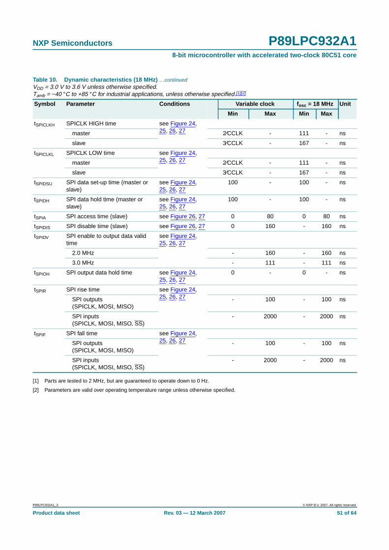
NXP Semiconductors P89LPC932A18-bit microcontroller with accelerated two-clock 80C51 core
[1] Parts are tested to 2 MHz, but are guaranteed to operate down to 0 Hz.
[2] Parameters are valid over operating temperature range unless otherwise specified.
tSPICLKH SPICLK HIGH time see Figure 24,25, 26, 27master 2⁄CCLK - 111 - ns
slave 3⁄CCLK - 167 - ns
tSPICLKL SPICLK LOW time see Figure 24,25, 26, 27master 2⁄CCLK - 111 - ns
slave 3⁄CCLK - 167 - ns
tSPIDSU SPI data set-up time (master orslave)
see Figure 24,25, 26, 27
100 - 100 - ns
tSPIDH SPI data hold time (master orslave)
see Figure 24,25, 26, 27
100 - 100 - ns
tSPIA SPI access time (slave) see Figure 26, 27 0 80 0 80 ns
tSPIDIS SPI disable time (slave) see Figure 26, 27 0 160 - 160 ns
tSPIDV SPI enable to output data validtime
see Figure 24,25, 26, 27
2.0 MHz - 160 - 160 ns
3.0 MHz - 111 - 111 ns
tSPIOH SPI output data hold time see Figure 24,25, 26, 27
0 - 0 - ns
tSPIR SPI rise time see Figure 24,25, 26, 27SPI outputs
(SPICLK, MOSI, MISO)- 100 - 100 ns
SPI inputs(SPICLK, MOSI, MISO, SS)
- 2000 - 2000 ns
tSPIF SPI fall time see Figure 24,25, 26, 27SPI outputs
(SPICLK, MOSI, MISO)- 100 - 100 ns
SPI inputs(SPICLK, MOSI, MISO, SS)
- 2000 - 2000 ns
Table 10. Dynamic characteristics (18 MHz) …continuedVDD = 3.0 V to 3.6 V unless otherwise specified.Tamb = −40 °C to +85 °C for industrial applications, unless otherwise specified.[1][2]
Symbol Parameter Conditions Variable clock fosc = 18 MHz Unit
Min Max Min Max
P89LPC932A1_3 © NXP B.V. 2007. All rights reserved.
Product data sheet Rev. 03 — 12 March 2007 51 of 64
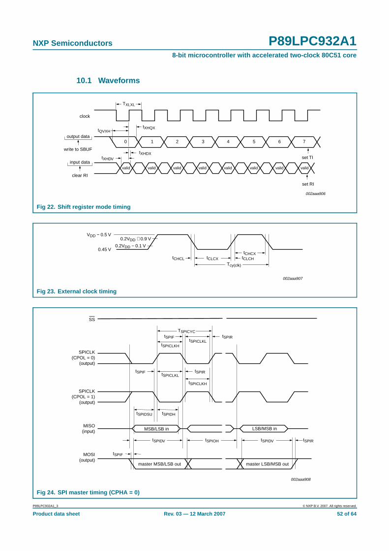
NXP Semiconductors P89LPC932A18-bit microcontroller with accelerated two-clock 80C51 core
10.1 Waveforms
Fig 22. Shift register mode timing
0 1 2 3 4 5 6 7
valid valid valid valid valid valid valid valid
TXLXL
002aaa906
set TI
set RI
tXHQXtQVXH
tXHDV
tXHDX
clock
output data
write to SBUF
input data
clear RI
Fig 23. External clock timing
tCHCL tCLCX
tCHCX
Tcy(clk)
tCLCH
002aaa907
0.2VDD + 0.9 V
0.2VDD − 0.1 V
VDD − 0.5 V
0.45 V
Fig 24. SPI master timing (CPHA = 0)
TSPICYC
tSPICLKH
tSPICLKH
tSPICLKL
tSPICLKL
master LSB/MSB outmaster MSB/LSB out
tSPIDHtSPIDSU
tSPIF
tSPIOH tSPIDV tSPIRtSPIDV
tSPIF tSPIR
tSPIF tSPIR
SS
SPICLK(CPOL = 0)
(output)
002aaa908
SPICLK(CPOL = 1)
(output)
MISO(input)
MOSI(output)
LSB/MSB inMSB/LSB in
P89LPC932A1_3 © NXP B.V. 2007. All rights reserved.
Product data sheet Rev. 03 — 12 March 2007 52 of 64
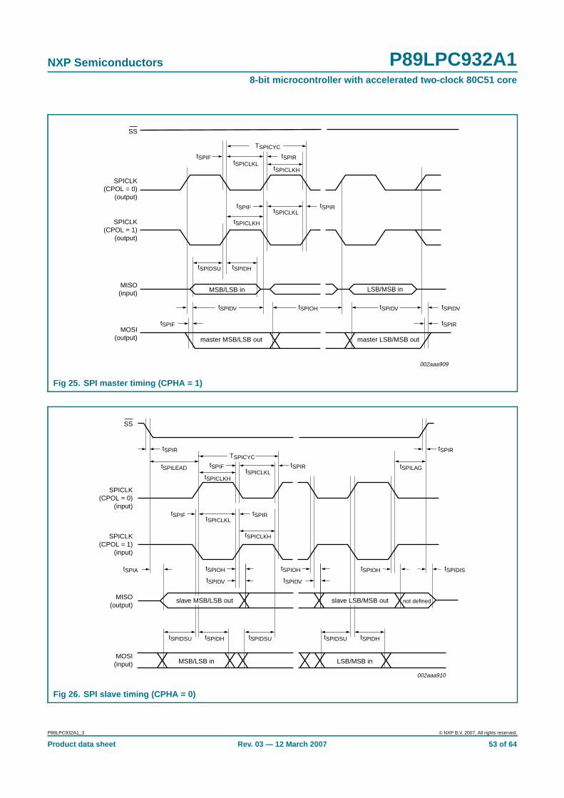
NXP Semiconductors P89LPC932A18-bit microcontroller with accelerated two-clock 80C51 core
Fig 25. SPI master timing (CPHA = 1)
TSPICYC
tSPICLKL
tSPICLKL
tSPICLKH
tSPICLKH
master LSB/MSB outmaster MSB/LSB out
tSPIDHtSPIDSU
tSPIF
tSPIOH tSPIDV tSPIDV
tSPIR
tSPIDV
tSPIF
tSPIF
tSPIR
tSPIR
SS
SPICLK(CPOL = 0)
(output)
002aaa909
SPICLK(CPOL = 1)
(output)
MISO(input)
MOSI(output)
LSB/MSB inMSB/LSB in
Fig 26. SPI slave timing (CPHA = 0)
TSPICYC
tSPICLKH
tSPICLKH
tSPICLKL
tSPICLKL
tSPILEAD tSPILAG
tSPIDSU tSPIDH tSPIDHtSPIDSU tSPIDSU
tSPIR
tSPIA tSPIOH tSPIDIS
tSPIR
slave MSB/LSB out
MSB/LSB in LSB/MSB in
slave LSB/MSB out
tSPIDV
tSPIOH tSPIOH
tSPIDV
tSPIR
tSPIR
tSPIF
tSPIF
SS
SPICLK(CPOL = 0)
(input)
002aaa910
SPICLK(CPOL = 1)
(input)
MISO(output)
MOSI(input)
not defined
P89LPC932A1_3 © NXP B.V. 2007. All rights reserved.
Product data sheet Rev. 03 — 12 March 2007 53 of 64
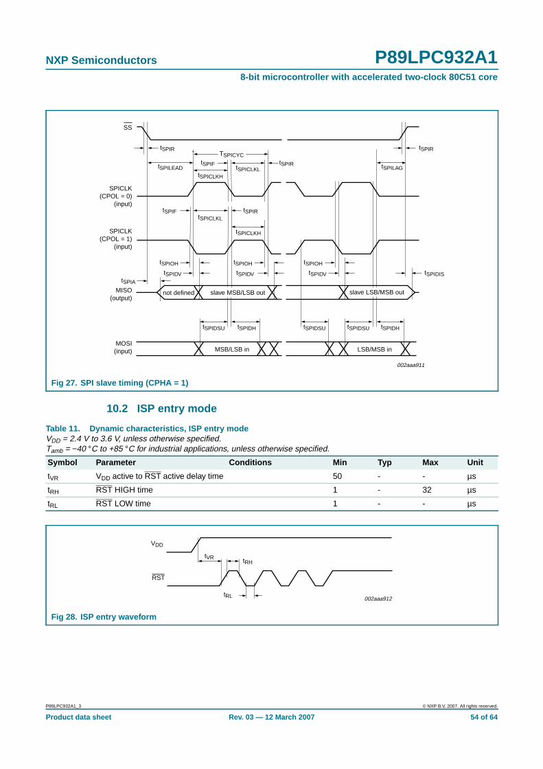
NXP Semiconductors P89LPC932A18-bit microcontroller with accelerated two-clock 80C51 core
10.2 ISP entry mode
Fig 27. SPI slave timing (CPHA = 1)
002aaa911
TSPICYC
tSPICLKH
tSPICLKH
tSPICLKLtSPILEAD
tSPICLKL
tSPILAG
tSPIDSU tSPIDSU tSPIDSUtSPIDH tSPIDH
tSPIR tSPIR
tSPIR
tSPIA
tSPIOH tSPIOH tSPIOH
tSPIDIS
slave MSB/LSB outnot defined
MSB/LSB in LSB/MSB in
slave LSB/MSB out
tSPIDV tSPIDV tSPIDV
tSPIRtSPIF
tSPIF
SS
SPICLK(CPOL = 0)
(input)
SPICLK(CPOL = 1)
(input)
MISO(output)
MOSI(input)
Table 11. Dynamic characteristics, ISP entry modeVDD = 2.4 V to 3.6 V, unless otherwise specified.Tamb = −40 °C to +85 °C for industrial applications, unless otherwise specified.
Symbol Parameter Conditions Min Typ Max Unit
tVR VDD active to RST active delay time 50 - - µs
tRH RST HIGH time 1 - 32 µs
tRL RST LOW time 1 - - µs
Fig 28. ISP entry waveform
002aaa912
VDD
RST
tRL
tVR tRH
P89LPC932A1_3 © NXP B.V. 2007. All rights reserved.
Product data sheet Rev. 03 — 12 March 2007 54 of 64
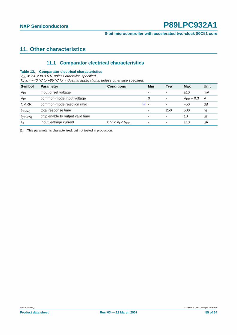
NXP Semiconductors P89LPC932A18-bit microcontroller with accelerated two-clock 80C51 core
11. Other characteristics
11.1 Comparator electrical characteristics
[1] This parameter is characterized, but not tested in production.
Table 12. Comparator electrical characteristicsVDD = 2.4 V to 3.6 V, unless otherwise specified.Tamb = −40 °C to +85 °C for industrial applications, unless otherwise specified.
Symbol Parameter Conditions Min Typ Max Unit
VIO input offset voltage - - ±10 mV
VIC common-mode input voltage 0 - VDD − 0.3 V
CMRR common-mode rejection ratio [1] - - −50 dB
tres(tot) total response time - 250 500 ns
t(CE-OV) chip enable to output valid time - - 10 µs
ILI input leakage current 0 V < VI < VDD - - ±10 µA
P89LPC932A1_3 © NXP B.V. 2007. All rights reserved.
Product data sheet Rev. 03 — 12 March 2007 55 of 64
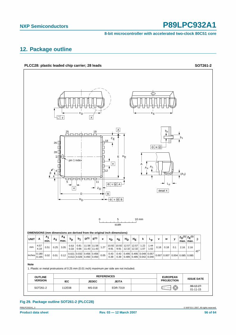
NXP Semiconductors P89LPC932A18-bit microcontroller with accelerated two-clock 80C51 core
12. Package outline
Fig 29. Package outline SOT261-2 (PLCC28)
REFERENCESOUTLINEVERSION
EUROPEANPROJECTION ISSUE DATE
IEC JEDEC JEITA
Note
1. Plastic or metal protrusions of 0.25 mm (0.01 inch) maximum per side are not included.
SOT261-2 112E08 MS-018 EDR-7319
1925
28
1
4
5 11
18
12
26
detail X
(A )3
bp
w M
A1A
A4
Lp
b1
βk
Xy
e
E
B
DH
EH
v M B
D
ZD
A
ZE
e
v M A
0 5 10 mm
scale
99-12-2701-11-15
pin 1 index
PLCC28: plastic leaded chip carrier; 28 leads SOT261-2
UNIT β
mm 4.574.19 0.51 3.05
0.530.33
0.0210.013
1.27 2.16
45o0.18 0.10.18
DIMENSIONS (mm dimensions are derived from the original inch dimensions)
11.5811.43
12.5712.32 2.16
0.810.66
1.221.07
0.1800.165 0.02 0.12
0.25
0.01 0.05 0.0850.007 0.0040.007
1.441.02
0.0570.040
0.4560.450
11.5811.43
0.4560.450
0.4950.485
12.5712.32
0.4950.485
10.929.91
0.430.39
10.929.91
0.430.39 0.085
0.0320.026
0.0480.042
Ee
inches
De
AA1
min.
A4max.
bp e ywvD(1) E(1) HD HEZD
(1)
max.ZE
(1)
max.b1 kA3 LpeD eE
P89LPC932A1_3 © NXP B.V. 2007. All rights reserved.
Product data sheet Rev. 03 — 12 March 2007 56 of 64
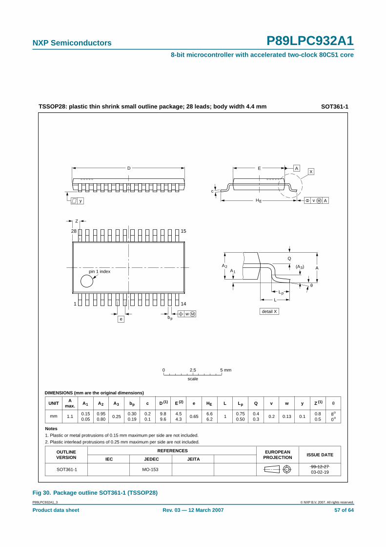
NXP Semiconductors P89LPC932A18-bit microcontroller with accelerated two-clock 80C51 core
Fig 30. Package outline SOT361-1 (TSSOP28)
UNIT A1 A2 A3 bp c D (1) E (2) (1)e HE L L p Q Zywv θ
REFERENCESOUTLINEVERSION
EUROPEANPROJECTION ISSUE DATE
IEC JEDEC JEITA
mm 0.150.05
0.950.80
0.300.19
0.20.1
9.89.6
4.54.3
0.656.66.2
0.40.3
0.80.5
80
o
o0.13 0.10.21
DIMENSIONS (mm are the original dimensions)
Notes
1. Plastic or metal protrusions of 0.15 mm maximum per side are not included.
2. Plastic interlead protrusions of 0.25 mm maximum per side are not included.
0.750.50
SOT361-1 MO-15399-12-2703-02-19
0.25
w Mbp
Z
e
1 14
28 15
pin 1 index
θ
AA1
A2
Lp
Q
detail X
L
(A )3
HE
E
c
v M A
XAD
y
0 2.5 5 mm
scale
TSSOP28: plastic thin shrink small outline package; 28 leads; body width 4.4 mm SOT361-1
Amax.
1.1
P89LPC932A1_3 © NXP B.V. 2007. All rights reserved.
Product data sheet Rev. 03 — 12 March 2007 57 of 64
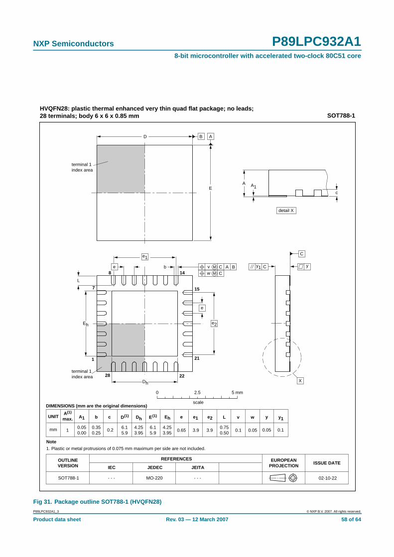
NXP Semiconductors P89LPC932A18-bit microcontroller with accelerated two-clock 80C51 core
Fig 31. Package outline SOT788-1 (HVQFN28)
0.651
A1 Ehb cUNIT ye
REFERENCESOUTLINEVERSION
EUROPEANPROJECTION ISSUE DATE
IEC JEDEC JEITA
mm 6.15.9
6.15.9
Dh
4.253.95
y1
4.253.95
e1
3.9
e2
3.90.350.25
0.050.00
0.2 0.05 0.1
DIMENSIONS (mm are the original dimensions)
SOT788-1 MO-220- - - - - -
0.750.50
L
0.1
v
0.05
w
0 2.5 5 mm
scale
SOT788-1HVQFN28: plastic thermal enhanced very thin quad flat package; no leads;28 terminals; body 6 x 6 x 0.85 mm
A(1)
max.
A A1c
detail X
yy1 Ce
L
Eh
Dh
e
e1
b8 14
28 22
21
157
1
X
D
E
C
B A
e2
02-10-22
terminal 1index area
terminal 1index area
ACC
Bv M
w M
Note
1. Plastic or metal protrusions of 0.075 mm maximum per side are not included.
D(1) E(1)
P89LPC932A1_3 © NXP B.V. 2007. All rights reserved.
Product data sheet Rev. 03 — 12 March 2007 58 of 64
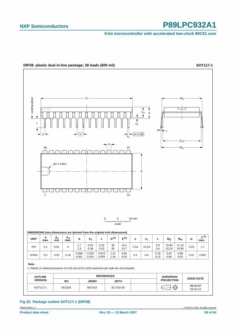
NXP Semiconductors P89LPC932A18-bit microcontroller with accelerated two-clock 80C51 core
Fig 32. Package outline SOT117-1 (DIP28)
UNIT Amax.
1 2 b1(1)
(1) (1)c D E we MHL
REFERENCESOUTLINEVERSION
EUROPEANPROJECTION ISSUE DATE
IEC JEDEC JEITA
mm
inches
DIMENSIONS (mm dimensions are derived from the original inch dimensions)
SOT117-199-12-2703-02-13
A min.
A max. b Z
max.MEe1
1.71.3
0.530.38
0.320.23
3635
14.113.7
3.93.4
0.252.54 15.2415.8015.24
17.1515.90
1.75.1 0.51 4
0.0660.051
0.0200.014
0.0130.009
1.411.34
0.560.54
0.150.13
0.010.1 0.60.620.60
0.680.63
0.0670.2 0.02 0.16
051G05 MO-015 SC-510-28
MH
c
(e )1
ME
A
L
seat
ing
plan
e
A1
w Mb1
e
D
A2
Z
28
1
15
14
b
E
pin 1 index
0 5 10 mm
scale
Note
1. Plastic or metal protrusions of 0.25 mm (0.01 inch) maximum per side are not included.
DIP28: plastic dual in-line package; 28 leads (600 mil) SOT117-1
P89LPC932A1_3 © NXP B.V. 2007. All rights reserved.
Product data sheet Rev. 03 — 12 March 2007 59 of 64
NXP Semiconductors P89LPC932A18-bit microcontroller with accelerated two-clock 80C51 core
13. Abbreviations
Table 13. Acronym list
Acronym Description
CCU Capture/Compare Unit
CPU Central Processing Unit
CRC Cyclic Redundancy Check
EPROM Erasable Programmable Read-Only Memory
EEPROM Electrically Erasable Programmable Read-Only Memory
EMI ElectroMagnetic Interference
LED Light Emitting Diode
PLL Phase-Locked Loop
PWM Pulse Width Modulator
RAM Random Access Memory
RC Resistance-Capacitance
RTC Real-Time Clock
SFR Special Function Register
SPI Serial Peripheral Interface
UART Universal Asynchronous Receiver/Transmitter
P89LPC932A1_3 © NXP B.V. 2007. All rights reserved.
Product data sheet Rev. 03 — 12 March 2007 60 of 64
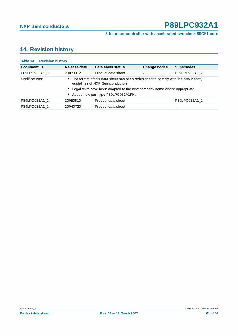
NXP Semiconductors P89LPC932A18-bit microcontroller with accelerated two-clock 80C51 core
14. Revision history
Table 14. Revision history
Document ID Release date Data sheet status Change notice Supersedes
P89LPC932A1_3 20070312 Product data sheet - P89LPC932A1_2
Modifications: • The format of this data sheet has been redesigned to comply with the new identityguidelines of NXP Semiconductors.
• Legal texts have been adapted to the new company name where appropriate.
• Added new part type P89LPC932A1FN.
P89LPC932A1_2 20050510 Product data sheet - P89LPC932A1_1
P89LPC932A1_1 20040720 Product data sheet - -
P89LPC932A1_3 © NXP B.V. 2007. All rights reserved.
Product data sheet Rev. 03 — 12 March 2007 61 of 64

NXP Semiconductors P89LPC932A18-bit microcontroller with accelerated two-clock 80C51 core
15. Legal information
15.1 Data sheet status
[1] Please consult the most recently issued document before initiating or completing a design.
[2] The term ‘short data sheet’ is explained in section “Definitions”.
[3] The product status of device(s) described in this document may have changed since this document was published and may differ in case of multiple devices. The latest product statusinformation is available on the Internet at URL http://www.nxp.com.
15.2 Definitions
Draft — The document is a draft version only. The content is still underinternal review and subject to formal approval, which may result inmodifications or additions. NXP Semiconductors does not give anyrepresentations or warranties as to the accuracy or completeness ofinformation included herein and shall have no liability for the consequences ofuse of such information.
Short data sheet — A short data sheet is an extract from a full data sheetwith the same product type number(s) and title. A short data sheet is intendedfor quick reference only and should not be relied upon to contain detailed andfull information. For detailed and full information see the relevant full datasheet, which is available on request via the local NXP Semiconductors salesoffice. In case of any inconsistency or conflict with the short data sheet, thefull data sheet shall prevail.
15.3 Disclaimers
General — Information in this document is believed to be accurate andreliable. However, NXP Semiconductors does not give any representations orwarranties, expressed or implied, as to the accuracy or completeness of suchinformation and shall have no liability for the consequences of use of suchinformation.
Right to make changes — NXP Semiconductors reserves the right to makechanges to information published in this document, including withoutlimitation specifications and product descriptions, at any time and withoutnotice. This document supersedes and replaces all information supplied priorto the publication hereof.
Suitability for use — NXP Semiconductors products are not designed,authorized or warranted to be suitable for use in medical, military, aircraft,space or life support equipment, nor in applications where failure ormalfunction of a NXP Semiconductors product can reasonably be expected to
result in personal injury, death or severe property or environmental damage.NXP Semiconductors accepts no liability for inclusion and/or use of NXPSemiconductors products in such equipment or applications and thereforesuch inclusion and/or use is at the customer’s own risk.
Applications — Applications that are described herein for any of theseproducts are for illustrative purposes only. NXP Semiconductors makes norepresentation or warranty that such applications will be suitable for thespecified use without further testing or modification.
Limiting values — Stress above one or more limiting values (as defined inthe Absolute Maximum Ratings System of IEC 60134) may cause permanentdamage to the device. Limiting values are stress ratings only and operation ofthe device at these or any other conditions above those given in theCharacteristics sections of this document is not implied. Exposure to limitingvalues for extended periods may affect device reliability.
Terms and conditions of sale — NXP Semiconductors products are soldsubject to the general terms and conditions of commercial sale, as publishedat http://www.nxp.com/profile/terms, including those pertaining to warranty,intellectual property rights infringement and limitation of liability, unlessexplicitly otherwise agreed to in writing by NXP Semiconductors. In case ofany inconsistency or conflict between information in this document and suchterms and conditions, the latter will prevail.
No offer to sell or license — Nothing in this document may be interpretedor construed as an offer to sell products that is open for acceptance or thegrant, conveyance or implication of any license under any copyrights, patentsor other industrial or intellectual property rights.
15.4 TrademarksNotice: All referenced brands, product names, service names and trademarksare the property of their respective owners.
I2C-bus — logo is a trademark of NXP B.V.
16. Contact information
For additional information, please visit: http://www .nxp.com
For sales office addresses, send an email to: salesad [email protected]
Document status [1] [2] Product status [3] Definition
Objective [short] data sheet Development This document contains data from the objective specification for product development.
Preliminary [short] data sheet Qualification This document contains data from the preliminary specification.
Product [short] data sheet Production This document contains the product specification.
P89LPC932A1_3 © NXP B.V. 2007. All rights reserved.
Product data sheet Rev. 03 — 12 March 2007 62 of 64
NXP Semiconductors P89LPC932A18-bit microcontroller with accelerated two-clock 80C51 core
17. Contents
1 General description . . . . . . . . . . . . . . . . . . . . . . 12 Features . . . . . . . . . . . . . . . . . . . . . . . . . . . . . . . 12.1 Principal features . . . . . . . . . . . . . . . . . . . . . . . 12.2 Additional features . . . . . . . . . . . . . . . . . . . . . . 12.3 Comparison to the P89LPC932 . . . . . . . . . . . . 23 Ordering information . . . . . . . . . . . . . . . . . . . . . 34 Block diagram . . . . . . . . . . . . . . . . . . . . . . . . . . 45 Functional diagram . . . . . . . . . . . . . . . . . . . . . . 56 Pinning information . . . . . . . . . . . . . . . . . . . . . . 56.1 Pinning . . . . . . . . . . . . . . . . . . . . . . . . . . . . . . . 56.2 Pin description . . . . . . . . . . . . . . . . . . . . . . . . . 77 Functional description . . . . . . . . . . . . . . . . . . 117.1 Special function registers . . . . . . . . . . . . . . . . 117.2 Enhanced CPU. . . . . . . . . . . . . . . . . . . . . . . . 177.3 Clocks . . . . . . . . . . . . . . . . . . . . . . . . . . . . . . . 177.3.1 Clock definitions . . . . . . . . . . . . . . . . . . . . . . . 177.3.2 CPU clock (OSCCLK). . . . . . . . . . . . . . . . . . . 177.3.3 Low speed oscillator option . . . . . . . . . . . . . . 177.3.4 Medium speed oscillator option . . . . . . . . . . . 177.3.5 High speed oscillator option . . . . . . . . . . . . . . 177.3.6 Clock output . . . . . . . . . . . . . . . . . . . . . . . . . . 177.4 On-chip RC oscillator option . . . . . . . . . . . . . . 187.5 Watchdog oscillator option . . . . . . . . . . . . . . . 187.6 External clock input option . . . . . . . . . . . . . . . 187.7 CCLK wake-up delay . . . . . . . . . . . . . . . . . . . 197.8 CCLK modification: DIVM register . . . . . . . . . 197.9 Low power select . . . . . . . . . . . . . . . . . . . . . . 197.10 Memory organization . . . . . . . . . . . . . . . . . . . 197.11 Data RAM arrangement . . . . . . . . . . . . . . . . . 207.12 Interrupts . . . . . . . . . . . . . . . . . . . . . . . . . . . . 207.12.1 External interrupt inputs . . . . . . . . . . . . . . . . . 207.13 I/O ports . . . . . . . . . . . . . . . . . . . . . . . . . . . . . 217.13.1 Port configurations . . . . . . . . . . . . . . . . . . . . . 227.13.1.1 Quasi-bidirectional output configuration . . . . . 227.13.1.2 Open-drain output configuration . . . . . . . . . . . 227.13.1.3 Input-only configuration . . . . . . . . . . . . . . . . . 227.13.1.4 Push-pull output configuration . . . . . . . . . . . . 237.13.2 Port 0 analog functions . . . . . . . . . . . . . . . . . . 237.13.3 Additional port features. . . . . . . . . . . . . . . . . . 237.14 Power monitoring functions. . . . . . . . . . . . . . . 237.14.1 Brownout detection . . . . . . . . . . . . . . . . . . . . . 237.14.2 Power-on detection . . . . . . . . . . . . . . . . . . . . . 247.15 Power reduction modes . . . . . . . . . . . . . . . . . 247.15.1 Idle mode . . . . . . . . . . . . . . . . . . . . . . . . . . . . 247.15.2 Power-down mode . . . . . . . . . . . . . . . . . . . . . 247.15.3 Total Power-down mode . . . . . . . . . . . . . . . . . 247.16 Reset . . . . . . . . . . . . . . . . . . . . . . . . . . . . . . . 24
7.16.1 Reset vector . . . . . . . . . . . . . . . . . . . . . . . . . . 257.17 Timers/counters 0 and 1 . . . . . . . . . . . . . . . . 257.17.1 Mode 0 . . . . . . . . . . . . . . . . . . . . . . . . . . . . . . 257.17.2 Mode 1 . . . . . . . . . . . . . . . . . . . . . . . . . . . . . . 267.17.3 Mode 2 . . . . . . . . . . . . . . . . . . . . . . . . . . . . . . 267.17.4 Mode 3 . . . . . . . . . . . . . . . . . . . . . . . . . . . . . . 267.17.5 Mode 6 . . . . . . . . . . . . . . . . . . . . . . . . . . . . . . 267.17.6 Timer overflow toggle output . . . . . . . . . . . . . 267.18 RTC/system timer. . . . . . . . . . . . . . . . . . . . . . 267.19 CCU . . . . . . . . . . . . . . . . . . . . . . . . . . . . . . . . 277.19.1 CCU clock . . . . . . . . . . . . . . . . . . . . . . . . . . . 277.19.2 CCUCLK prescaling . . . . . . . . . . . . . . . . . . . . 277.19.3 Basic timer operation . . . . . . . . . . . . . . . . . . . 277.19.4 Output compare . . . . . . . . . . . . . . . . . . . . . . . 277.19.5 Input capture . . . . . . . . . . . . . . . . . . . . . . . . . 277.19.6 PWM operation . . . . . . . . . . . . . . . . . . . . . . . 287.19.7 Alternating output mode. . . . . . . . . . . . . . . . . 297.19.8 PLL operation. . . . . . . . . . . . . . . . . . . . . . . . . 297.19.9 CCU interrupts . . . . . . . . . . . . . . . . . . . . . . . . 307.20 UART . . . . . . . . . . . . . . . . . . . . . . . . . . . . . . . 307.20.1 Mode 0 . . . . . . . . . . . . . . . . . . . . . . . . . . . . . . 307.20.2 Mode 1 . . . . . . . . . . . . . . . . . . . . . . . . . . . . . . 307.20.3 Mode 2 . . . . . . . . . . . . . . . . . . . . . . . . . . . . . . 317.20.4 Mode 3 . . . . . . . . . . . . . . . . . . . . . . . . . . . . . . 317.20.5 Baud rate generator and selection . . . . . . . . . 317.20.6 Framing error . . . . . . . . . . . . . . . . . . . . . . . . . 317.20.7 Break detect . . . . . . . . . . . . . . . . . . . . . . . . . . 317.20.8 Double buffering . . . . . . . . . . . . . . . . . . . . . . . 327.20.9 Transmit interrupts with double buffering
enabled (modes 1, 2 and 3) . . . . . . . . . . . . . . 327.20.10 The 9th bit (bit 8) in double buffering
(modes 1, 2 and 3) . . . . . . . . . . . . . . . . . . . . . 327.21 I2C-bus serial interface. . . . . . . . . . . . . . . . . . 337.22 Serial Peripheral Interface (SPI). . . . . . . . . . . 357.22.1 Typical SPI configurations . . . . . . . . . . . . . . . 367.23 Analog comparators . . . . . . . . . . . . . . . . . . . . 387.23.1 Internal reference voltage. . . . . . . . . . . . . . . . 387.23.2 Comparator interrupt . . . . . . . . . . . . . . . . . . . 387.23.3 Comparators and power reduction modes . . . 397.24 Keypad interrupt . . . . . . . . . . . . . . . . . . . . . . . 397.25 Watchdog timer . . . . . . . . . . . . . . . . . . . . . . . 407.26 Additional features . . . . . . . . . . . . . . . . . . . . . 407.26.1 Software reset . . . . . . . . . . . . . . . . . . . . . . . . 407.26.2 Dual data pointers . . . . . . . . . . . . . . . . . . . . . 407.27 Data EEPROM . . . . . . . . . . . . . . . . . . . . . . . . 417.28 Flash program memory . . . . . . . . . . . . . . . . . 417.28.1 General description . . . . . . . . . . . . . . . . . . . . 417.28.2 Features . . . . . . . . . . . . . . . . . . . . . . . . . . . . . 41
P89LPC932A1_3 © NXP B.V. 2007. All rights reserved.
Product data sheet Rev. 03 — 12 March 2007 63 of 64
continued >>
NXP Semiconductors P89LPC932A18-bit microcontroller with accelerated two-clock 80C51 core
7.28.3 Flash organization . . . . . . . . . . . . . . . . . . . . . 427.28.4 Using flash as data storage . . . . . . . . . . . . . . 427.28.5 Flash programming and erasing . . . . . . . . . . . 427.28.6 In-circuit programming . . . . . . . . . . . . . . . . . . 427.28.7 In-application programming . . . . . . . . . . . . . . 427.28.8 In-system programming . . . . . . . . . . . . . . . . . 437.28.9 Power-on reset code execution. . . . . . . . . . . . 437.28.10 Hardware activation of the boot loader . . . . . . 437.29 User configuration bytes . . . . . . . . . . . . . . . . . 447.30 User sector security bytes . . . . . . . . . . . . . . . 448 Limiting values. . . . . . . . . . . . . . . . . . . . . . . . . 459 Static characteristics. . . . . . . . . . . . . . . . . . . . 4610 Dynamic characteristics . . . . . . . . . . . . . . . . . 4810.1 Waveforms . . . . . . . . . . . . . . . . . . . . . . . . . . . 5210.2 ISP entry mode. . . . . . . . . . . . . . . . . . . . . . . . 5411 Other characteristics . . . . . . . . . . . . . . . . . . . . 5511.1 Comparator electrical characteristics . . . . . . . 5512 Package outline . . . . . . . . . . . . . . . . . . . . . . . . 5613 Abbreviations . . . . . . . . . . . . . . . . . . . . . . . . . . 6014 Revision history . . . . . . . . . . . . . . . . . . . . . . . . 6115 Legal information. . . . . . . . . . . . . . . . . . . . . . . 6215.1 Data sheet status . . . . . . . . . . . . . . . . . . . . . . 6215.2 Definitions . . . . . . . . . . . . . . . . . . . . . . . . . . . . 6215.3 Disclaimers . . . . . . . . . . . . . . . . . . . . . . . . . . . 6215.4 Trademarks . . . . . . . . . . . . . . . . . . . . . . . . . . . 6216 Contact information. . . . . . . . . . . . . . . . . . . . . 6217 Contents . . . . . . . . . . . . . . . . . . . . . . . . . . . . . . 63
© NXP B.V. 2007. All rights reserved.For more information, please visit: http://www.nxp.comFor sales office addresses, please send an email to: [email protected]
Date of release: 12 March 2007
Document identifier: P89LPC932A1_3
Please be aware that important notices concerning this document and the product(s)described herein, have been included in section ‘Legal information’.