overview of nanowires and nanotubes -...
TRANSCRIPT
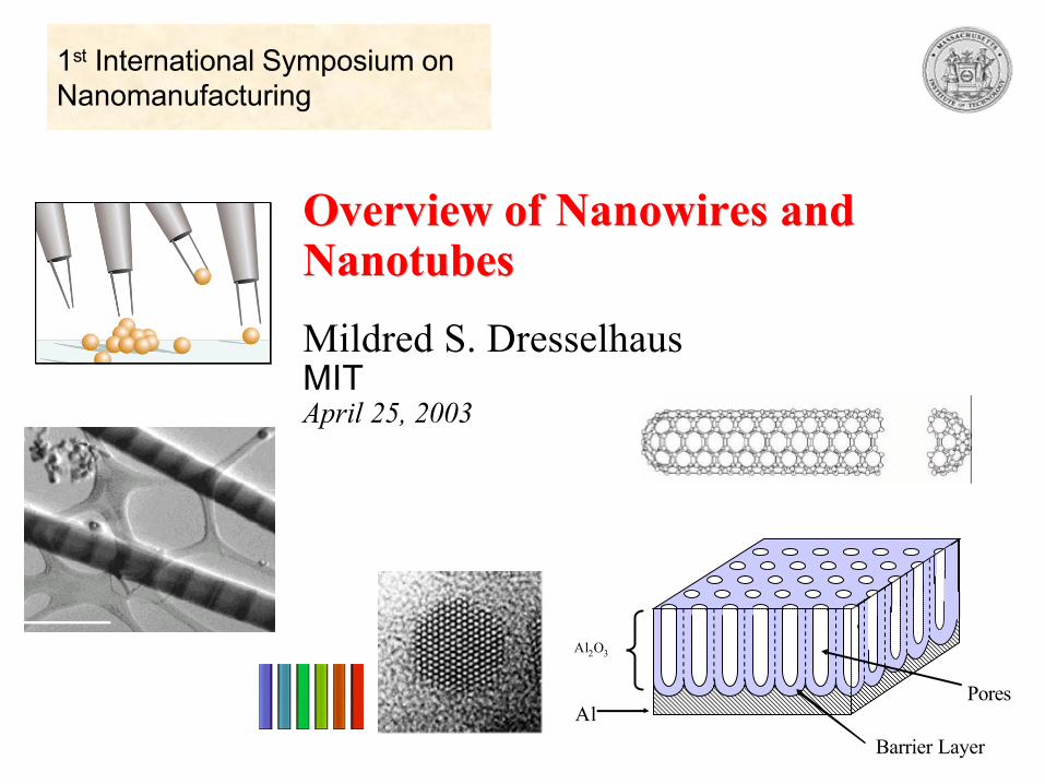
Overview of Overview of NanowiresNanowires and and NanotubesNanotubes
Mildred S. DresselhausMITApril 25, 2003
1st International Symposium on Nanomanufacturing
Al
Al2O3
Barrier Layer
Pores
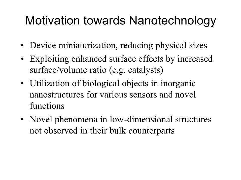
Motivation towards Nanotechnology
• Device miniaturization, reducing physical sizes• Exploiting enhanced surface effects by increased
surface/volume ratio (e.g. catalysts)• Utilization of biological objects in inorganic
nanostructures for various sensors and novel functions
• Novel phenomena in low-dimensional structures not observed in their bulk counterparts
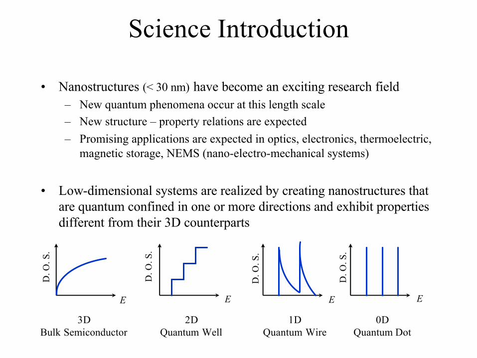
Science Introduction
• Nanostructures (< 30 nm) have become an exciting research field– New quantum phenomena occur at this length scale– New structure – property relations are expected– Promising applications are expected in optics, electronics, thermoelectric,
magnetic storage, NEMS (nano-electro-mechanical systems)
• Low-dimensional systems are realized by creating nanostructures thatare quantum confined in one or more directions and exhibit properties different from their 3D counterparts
3DBulk Semiconductor
2DQuantum Well
1DQuantum Wire
0DQuantum Dot
E
D. O
. S.
D. O
. S.
D. O
. S.
D. O
. S.
E E E
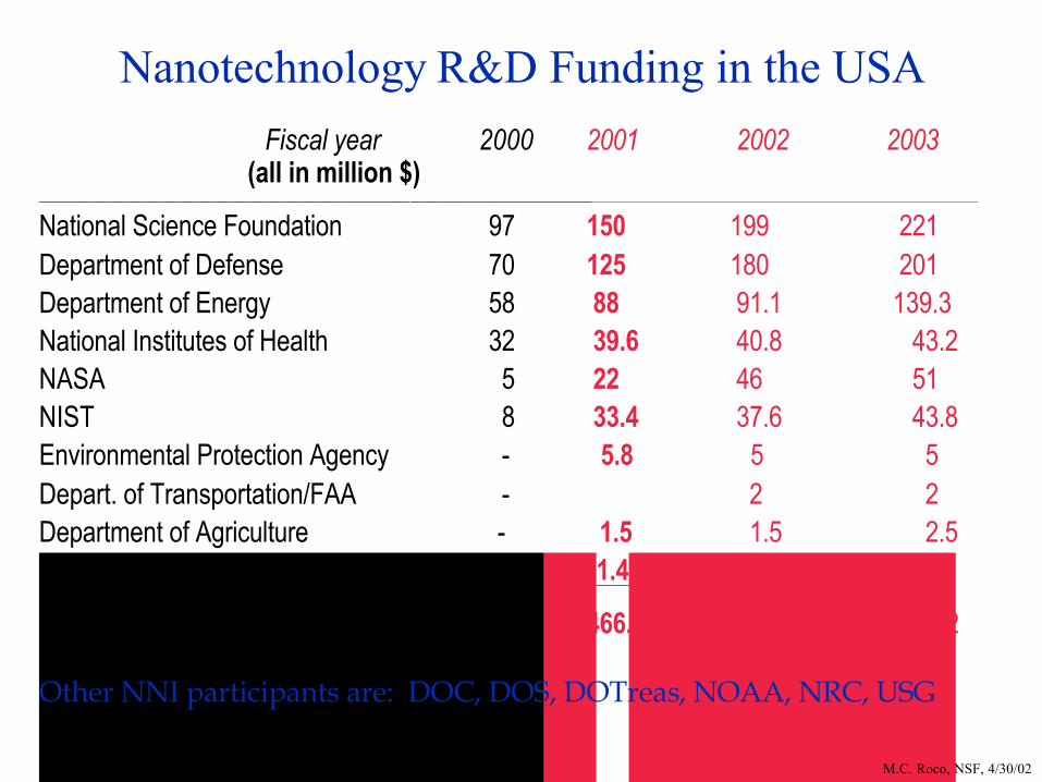
Nanotechnology R&D Funding in the USAFiscal year 2000 2001 2002 2003
(all in million $)__________________________________________________________________________________________________________________________________________________________________
National Science Foundation 97 150 199 221Department of Defense 70 125 180 201Department of Energy 58 88 91.1 139.3National Institutes of Health 32 39.6 40.8 43.2 NASA 5 22 46 51 NIST 8 33.4 37.6 43.8 Environmental Protection Agency - 5.8 5 5Depart. of Transportation/FAA - 2 2Department of Agriculture - 1.5 1.5 2.5Department of Justice - 1.4 1.4 1.4
TOTAL 270.0 466.7 604.4 710.2
Other NNI participants are: DOC, DOS, DOTreas, NOAA, NRC, USG
M.C. Roco, NSF, 4/30/02

0
500
1000
1500
2000
2500
1997 1998 1999 2000 2001 2002
mil
lion
s $
/ ye
ar
W. Europe
Japan
USA
OthersTotal
Senate Briefing, May 24, 2001 (M.C. Roco), updated on February 5, 2002
• U.S. begins FY in October, six month before EU & Japan in March/April
• U.S. does not have a commanding lead as it was for other S&T megatrends(such as BIO, IT, space exploration, nuclear)
Context Context –– Nanotechnology in the WorldNanotechnology in the WorldGovernment investments 1997Government investments 1997--20022002
Note:
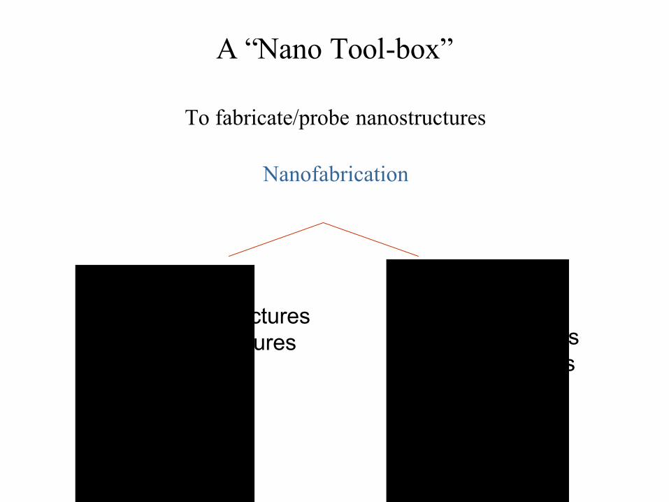
A “Nano Tool-box”
To fabricate/probe nanostructures
Nanofabrication
Top-down Method
- create nanostructures out of macrostructures
Bottom-up Method
- self assembly of atoms or molecules into nanostructures

(a) Bi Nanowire (b) Bi Nanotube (c) Bi Atomic Line
Various Nanostructures can occur in 1DEach have different structure/properties
Selectivity is therefore important
K. MikiETL,Japan
Peidong YangUC Berkeley
Dresselhaus Group(MIT)

Wiring on Si with ultra-fine Bi linesStructure different from 3D Bismuth
Bi nanoline
• Features:• over 300 nm long• 1 nm (3 Si dimers) wide• without kink• in terrace (not on top layer)K. Miki et al. Surf. Sci. 421 (1999) 397
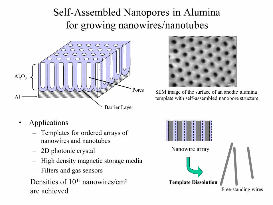
Self-Assembled Nanopores in Aluminafor growing nanowires/nanotubes
• Applications– Templates for ordered arrays of
nanowires and nanotubes– 2D photonic crystal– High density magnetic storage media– Filters and gas sensors
Al
Al2O3
Barrier Layer
Pores
Free-standing wires
Nanowire array
SEM image of the surface of an anodic aluminatemplate with self-assembled nanopore structure
Template DissolutionDensities of 1011 nanowires/cm2
are achieved
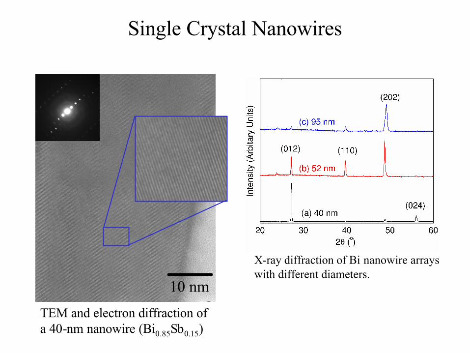
Single Crystal Nanowires
10 nm
TEM and electron diffraction of a 40-nm nanowire (Bi0.85Sb0.15)
X-ray diffraction of Bi nanowire arrays with different diameters.
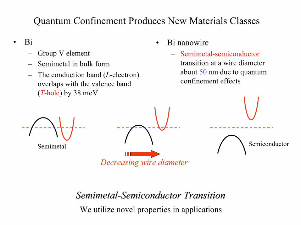
Quantum Confinement Produces New Materials Classes
• Bi – Group V element– Semimetal in bulk form– The conduction band (L-electron)
overlaps with the valence band (T-hole) by 38 meV
Decreasing wire diameter
Semimetal Semiconductor
• Bi nanowire– Semimetal-semiconductor
transition at a wire diameter about 50 nm due to quantum confinement effects
SemimetalSemimetal--Semiconductor TransitionSemiconductor TransitionWe utilize novel properties in applications

Why nanostructures are useful for thermoelectrics
ZTS T
?2??
Seebeck Coefficient ConductivityTemperature
ThermalConductivity
ZT ~ 3 for conventional refrigerators
Difficulties in increasing ZT in bulk materials:
S ? ? ? ? ?
? ? ? ? S ? and ??
? A limit to Z is rapidly obtained in conventional materials
? So far, best bulk material (Bi0.5Sb1.5Te3)has ZT ~ 1 at 300 K
Low dimensions give independent control of variables:? Enhanced density of states due to quantum confinement effects
? Increases S without reducing ?? Boundary scattering at interfaces reduces ? more than ?? Possibility of carrier pocket engineering to further improve ZT

Anodic Alumina on Silicon Wafers -Motivation
• Elimination of unfavorable fabrication steps.• Rigid substrate, affords extended crack-free films.• Low surface roughness.• Solution to the barrier layer problem for electrical connects.• Incorporation into electronic, optical devices on the wafer.• Combined nano-scale and micro-scale patterning.
Fabrication of the porous alumina templates on silicon substrates is an appealing improvement over the conventional fabrication process for the following reasons:
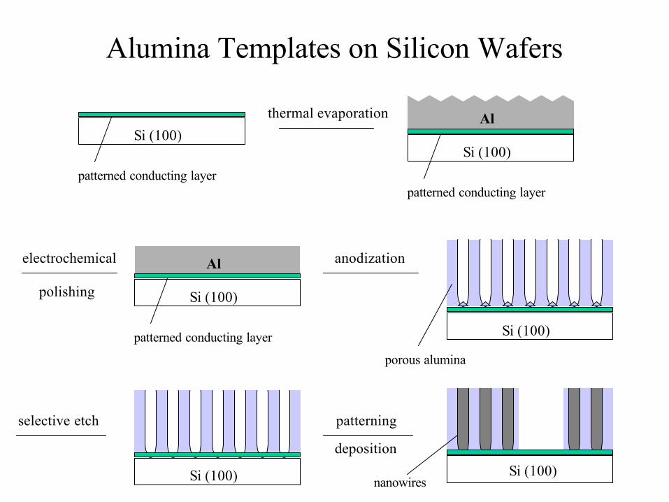
Alumina Templates on Silicon Wafers
Si (100)
patterned conducting layer
thermal evaporation
Si (100)
patterned conducting layer
electrochemical
Si (100)
patterned conducting layer
Al
polishing
anodization
Si (100)
Si (100)
deposition
porous alumina
nanowires
Al
selective etch patterning
Si (100)
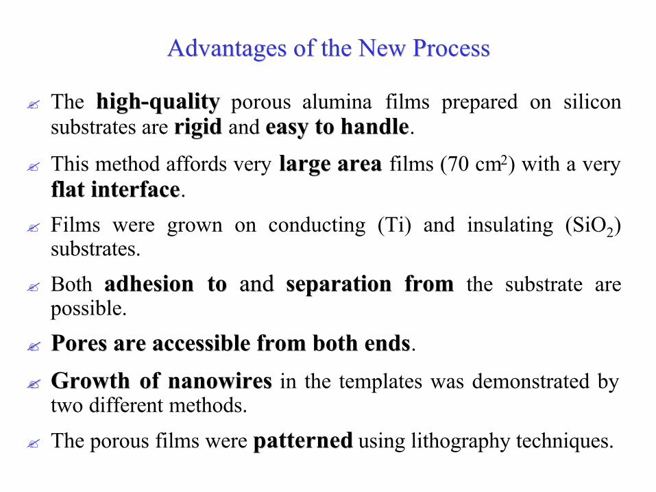
Advantages of the New ProcessAdvantages of the New Process
? The highhigh--qualityquality porous alumina films prepared on silicon substrates are rigidrigid and easy to handleeasy to handle.
? This method affords very large arealarge area films (70 cm2) with a very flat interfaceflat interface.
? Films were grown on conducting (Ti) and insulating (SiO2) substrates.
? Both adhesion to adhesion to andand separation from separation from the substrate are possible.
?? Pores are accessible from both endsPores are accessible from both ends.
?? Growth ofGrowth of nanowiresnanowires in the templates was demonstrated by two different methods.
? The porous films were patternedpatterned using lithography techniques.
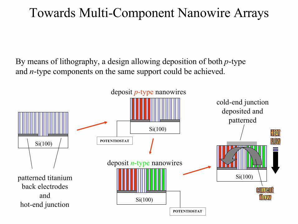
Towards Multi-Component Nanowire Arrays
By means of lithography, a design allowing deposition of both p-type and n-type components on the same support could be achieved.
patterned titaniumback electrodes
andhot-end junction
deposit p-type nanowirescold-end junction
deposited and patterned
Si(100)
Si(100)
Si(100)
POTENTIOSTAT
Si(100)
POTENTIOSTAT
deposit n-type nanowires

Structural Features
Ti
Si
Al
Oblique View Cross Section
The new Al2O3/Si structure conserves the dense uniform porous morphology with long channels, but consists of a thinner barrier layer.
ForComparison
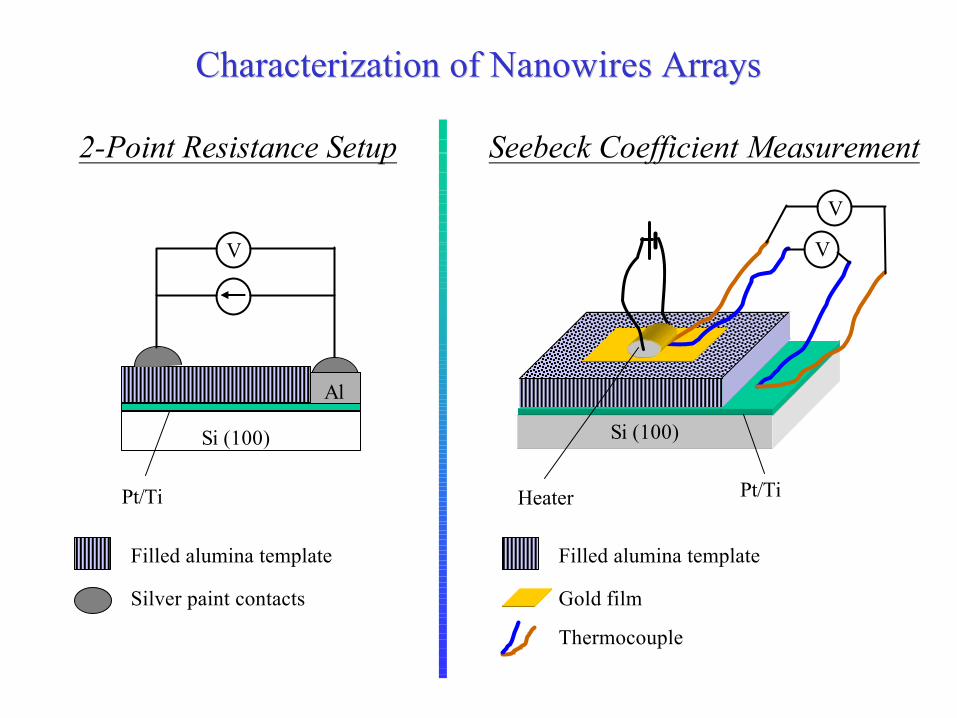
Characterization of Characterization of NanowiresNanowires ArraysArrays
Filled alumina template
Silver paint contacts
Al
Si (100)
Pt/Ti
V
2-Point Resistance Setup Seebeck Coefficient Measurement
V
V
Si (100)
Pt/TiHeater
Filled alumina template
Gold film
Thermocouple
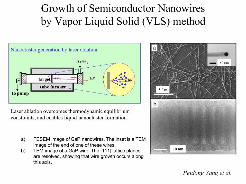
Growth of Semiconductor Nanowiresby Vapor Liquid Solid (VLS) method
a) FESEM image of GaP nanowires. The inset is a TEM image of the end of one of these wires.
b) TEM image of a GaP wire. The [111] lattice planes are resolved, showing that wire growth occurs along this axis.
5 ? m
50 n m
10 nm
Peidong Yang et al.
Laser ablation overcomes thermodynamic equilibrium constraints, and enables liquid nanocluster formation.
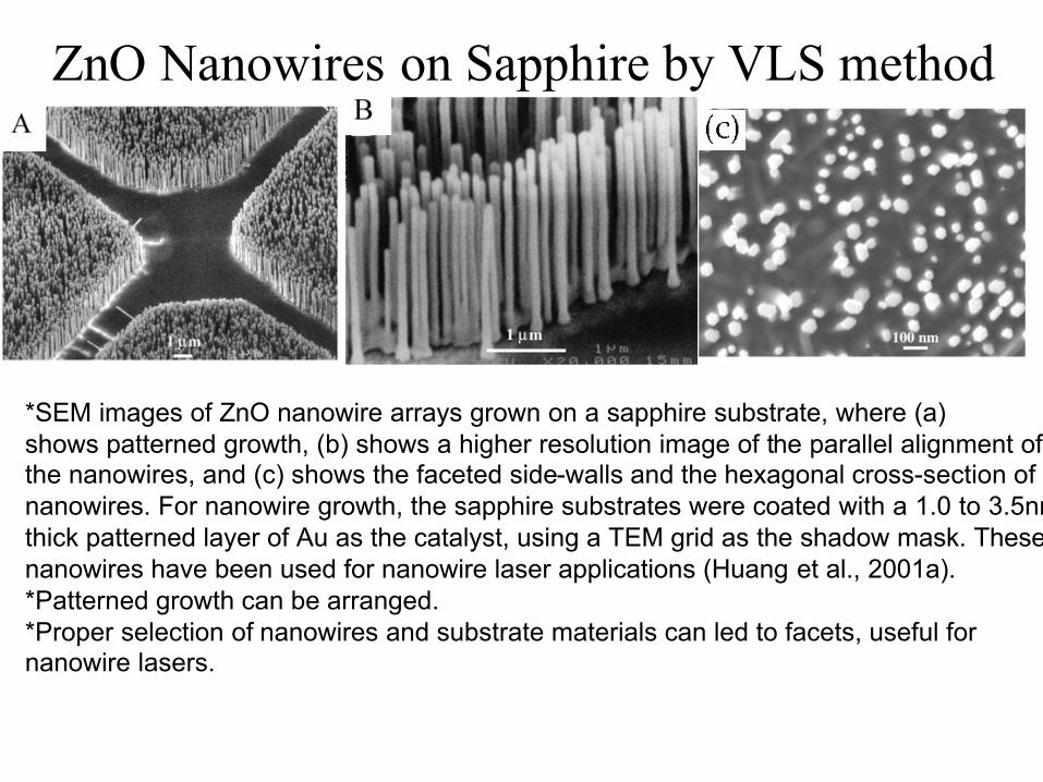
*SEM images of ZnO nanowire arrays grown on a sapphire substrate, where (a)shows patterned growth, (b) shows a higher resolution image of the parallel alignment ofthe nanowires, and (c) shows the faceted side-walls and the hexagonal cross-section of thenanowires. For nanowire growth, the sapphire substrates were coated with a 1.0 to 3.5nmthick patterned layer of Au as the catalyst, using a TEM grid as the shadow mask. Thesenanowires have been used for nanowire laser applications (Huang et al., 2001a).*Patterned growth can be arranged.*Proper selection of nanowires and substrate materials can led to facets, useful for nanowire lasers.
ZnO Nanowires on Sapphire by VLS method
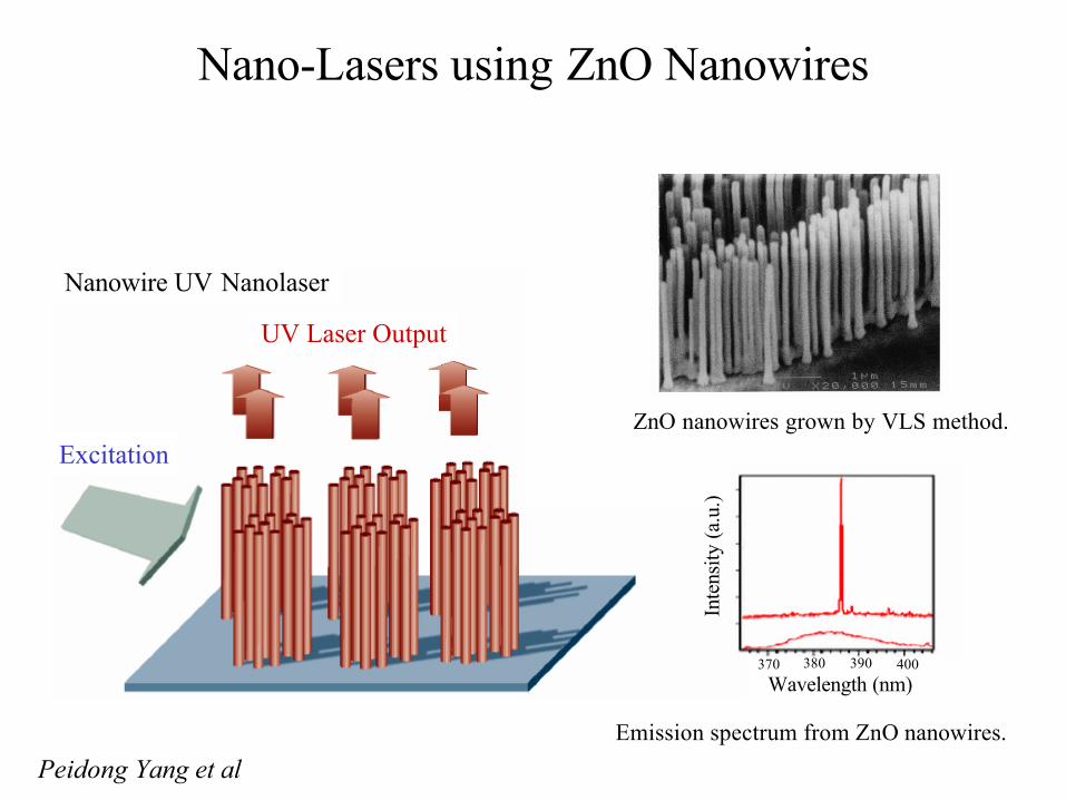
Nano-Lasers using ZnO Nanowires
ZnO nanowires grown by VLS method.
Emission spectrum from ZnO nanowires.
Peidong Yang et al
Wavelength (nm)370 380 390 400
Inte
nsity
(a.u
.)
Nanowire UV Nanolaser
UV Laser Output
Excitation
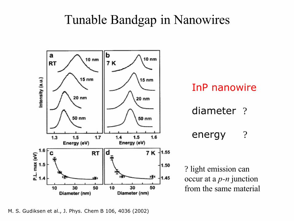
Tunable Bandgap in Nanowires
InP nanowire
diameter ?
energy ?
M. S. Gudiksen et al., J. Phys. Chem B 106, 4036 (2002)
? light emission canoccur at a p-n junction from the same material
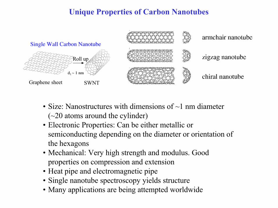
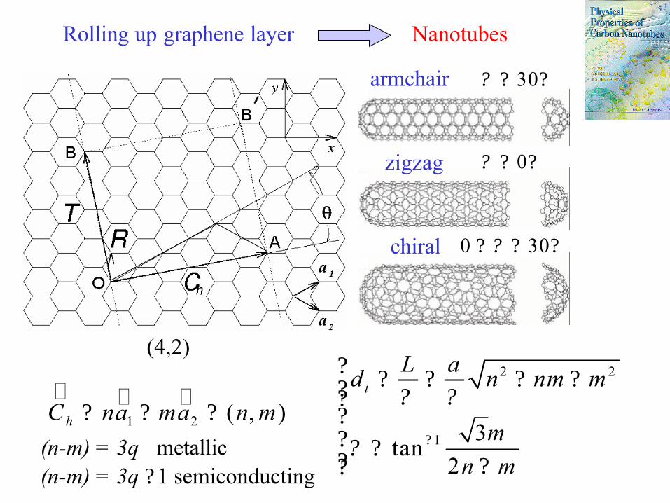
Unique Properties of Carbon Nanotubes
• Size: Nanostructures with dimensions of ~1 nm diameter (~20 atoms around the cylinder)
• Electronic Properties: Can be either metallic or semiconducting depending on the diameter or orientation of the hexagons
• Mechanical: Very high strength and modulus. Good properties on compression and extension
• Heat pipe and electromagnetic pipe• Single nanotube spectroscopy yields structure• Many applications are being attempted worldwide
Graphene sheet SWNT
Roll up
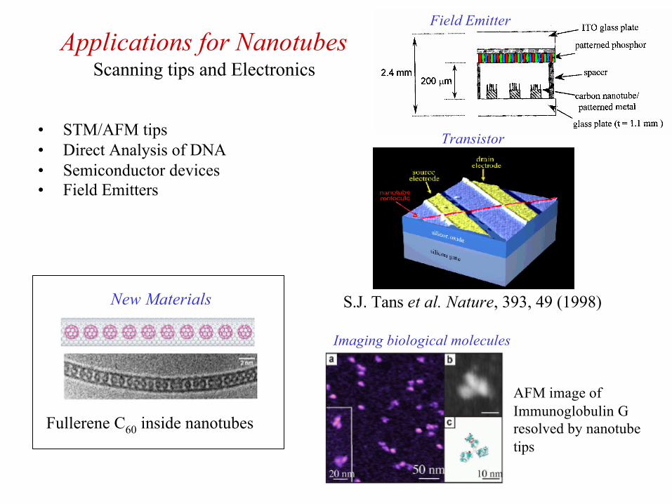
Applications for NanotubesScanning tips and Electronics
• STM/AFM tips• Direct Analysis of DNA• Semiconductor devices• Field Emitters
S.J. Tans et al. Nature, 393, 49 (1998)
AFM image of Immunoglobulin G resolved by nanotube tips
Field Emitter
Transistor
Imaging biological molecules
New Materials
Fullerene C60 inside nanotubes
2 2
1 21
( , )3
tan2
t
h
L ad n nm m
C na ma n mm
n m
? ?
? ?
? ? ? ? ???? ? ? ?? ?? ??
? ? ?
(4,2)
Rolling up graphene layer
0? ? ?
0 30?? ? ?
30? ? ?armchair
zigzag
chiral
Nanotubes
(n-m) = 3q metallic(n-m) = 3q ?1 semiconducting
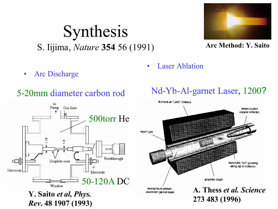
SynthesisS. Iijima, Nature 354 56 (1991)
• Arc Discharge• Laser Ablation
5-20mm diameter carbon rod Nd-Yb-Al-garnet Laser, 1200?
Y. Saito et al, Phys. Rev. 48 1907 (1993)
A. Thess et al. Science273 483 (1996)
Arc Method: Y. Saito
50-120A DC
500torr He
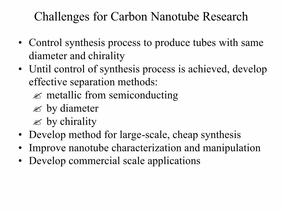
Challenges for Carbon Nanotube Research
• Control synthesis process to produce tubes with same diameter and chirality
• Until control of synthesis process is achieved, develop effective separation methods:? metallic from semiconducting? by diameter? by chirality
• Develop method for large-scale, cheap synthesis• Improve nanotube characterization and manipulation • Develop commercial scale applications
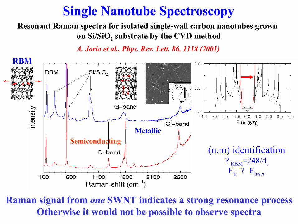
Resonant Raman spectra for isolated single-wall carbon nanotubes grown on Si/SiO2 substrate by the CVD method
RBM
SemiconductingMetallic
(n,m) identification? RBM=248/dtEii ? Elaser
A. Jorio et al., Phys. Rev. Lett. 86, 1118 (2001)
Raman signal from Raman signal from one one SWNT indicates a strong resonance processSWNT indicates a strong resonance processOtherwise it would not be possible to observe spectraOtherwise it would not be possible to observe spectra
'
Single Nanotube SpectroscopySingle Nanotube Spectroscopy

SEPARATION PROCESSSEPARATION PROCESS
AcidAcid--treated SWNT material nontreated SWNT material non--covalentlycovalently functionalizedfunctionalizedwith with octadecylamineoctadecylamine (ODA) and dispersed in (ODA) and dispersed in tetrahydrofurantetrahydrofuran(THF) is immersed in a water bath to accelerate precipitation.(THF) is immersed in a water bath to accelerate precipitation.VacuumVacuum--dried precipitate and supernatant are studied.dried precipitate and supernatant are studied.
The ODA organization on metallic (M) SWNTs is selectivelyThe ODA organization on metallic (M) SWNTs is selectivelydestabilized promoting their preferential precipitation, whiledestabilized promoting their preferential precipitation, whilethe supernatant is enriched in semiconducting (S) SWNTs.the supernatant is enriched in semiconducting (S) SWNTs.
What is the relative amount of precipitate and supernatantWhat is the relative amount of precipitate and supernatantSWNT material compared to asSWNT material compared to as--supplied samplesupplied sample ??????
Separation method developed by Fotios Papadimitrakopolousof the University of Connecticut

Determination of nanotube diameter distribution from RBMDetermination of nanotube diameter distribution from RBM
HiPcoHiPco RAMAN RAMAN ArAr ion 514 nm (2.41 eV)ion 514 nm (2.41 eV) 1.36 nm1.04 nm0.78 nm
MM BWFBWF
asas--suppliedsupplied asas--suppliedsupplied? RBM ? dt ? ? G? ? 1517,1532,1564cm?1 (exp. 1524,1548,1571cm?1 )
Continuum approximationContinuum approximation:: H. Kuzmany et al EPJ B 22 307 (2001)The Eii bands are treated as a continuum of states rather than individual VHSs. This model results in
SS SS
MM?? SS
SS SSMMMM
MM
(A)
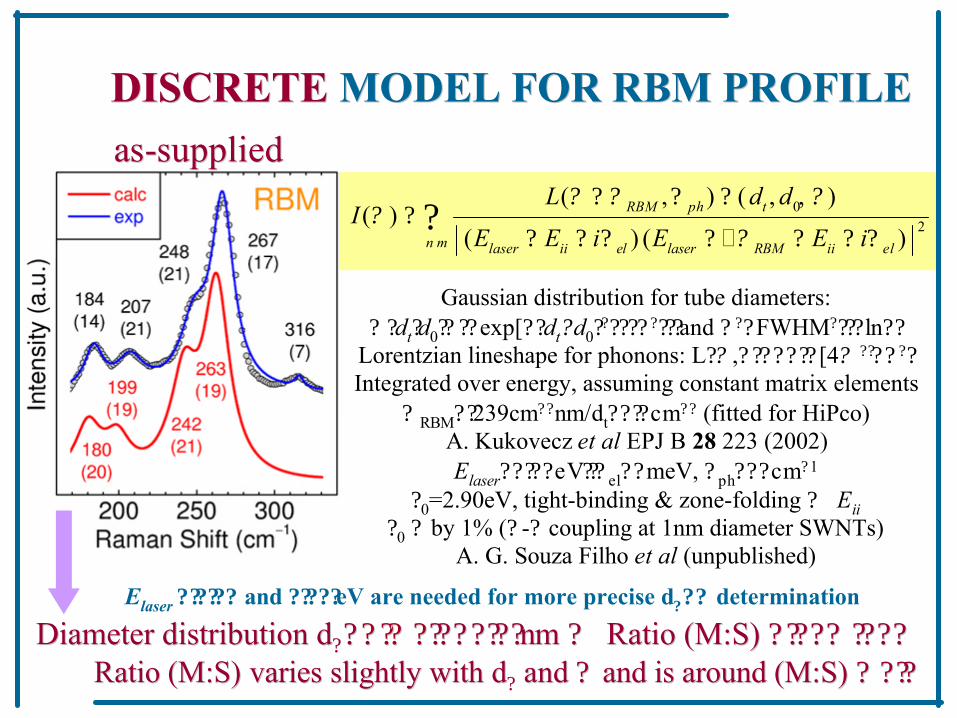
DISCRETEDISCRETE MODEL FOR RBM PROFILEMODEL FOR RBM PROFILEasas--suppliedsupplied
02
( , ) ( , , )( )
( ) ( )RBM ph t
n m laser ii el laser RBM ii el
L d dI
E E i E E i
? ? ??
?
? ? ??
? ? ? ? ? ? ??
?
Gaussian distribution for tube diameters:? ?dt?d0?? ??exp[??dt?d0?????? ????and ? ??FWHM????ln??
Lorentzian lineshape for phonons: L?? ,? ??????[4? ???? ??Integrated over energy, assuming constant matrix elements
? RBM??239cm??nm/dt????cm?? (fitted for HiPco)A. Kukovecz et al EPJ B 28 223 (2002)Elaser?????eV??? el??meV, ? ph???cm?1
?0=2.90eV, tight-binding & zone-folding ? Eii?0 ? by 1% (? -? coupling at 1nm diameter SWNTs)
A. G. Souza Filho et al (unpublished)
Diameter distribution dDiameter distribution d???? ? ?? ??? ???????? ????????nm nm ?? Ratio (M:S) Ratio (M:S) ????? ????????? ????Ratio (M:S) Ratio (M:S) varies slightly with dvaries slightly with d?? and and ?? and is around and is around (M:S) (M:S) ?? ??????
Elaser ?????? and ?????eV are needed for more precise d??? determination
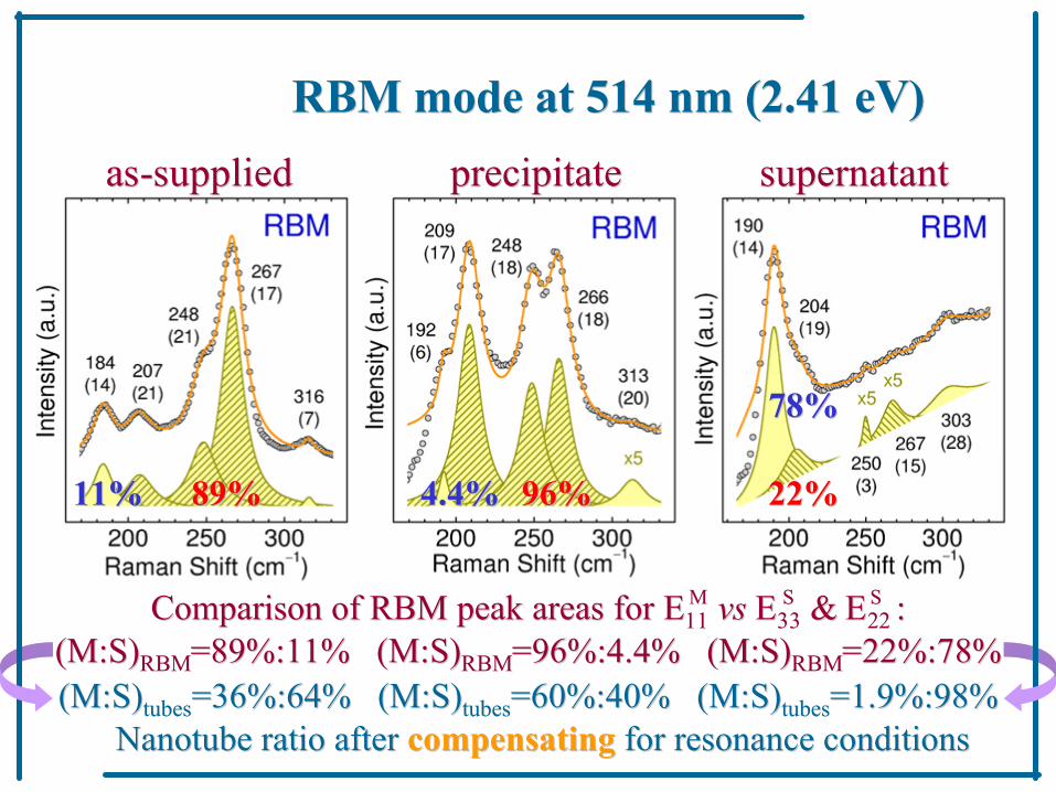
RBM mode at 514 nm (2.41 eV)RBM mode at 514 nm (2.41 eV)
precipitateprecipitate supernatantsupernatantasas--suppliedsupplied
11%11% 4.4%4.4%
78%78%
89%89% 96%96% 22%22%
(M:S)(M:S)tubestubes=36%:64% (M:S)=36%:64% (M:S)tubestubes=60%:40% (M:S)=60%:40% (M:S)tubestubes=1.9%:98%=1.9%:98%Nanotube ratio after Nanotube ratio after compensatingcompensating for resonance conditionsfor resonance conditions
Comparison of RBM peak areas for EComparison of RBM peak areas for E1111 vsvs EE3333 & E& E22 22 ::(M:S)(M:S)RBMRBM=89%:11% (M:S)=89%:11% (M:S)RBMRBM=96%:4.4% (M:S)=96%:4.4% (M:S)RBMRBM=22%:78%=22%:78%
MM S SS S
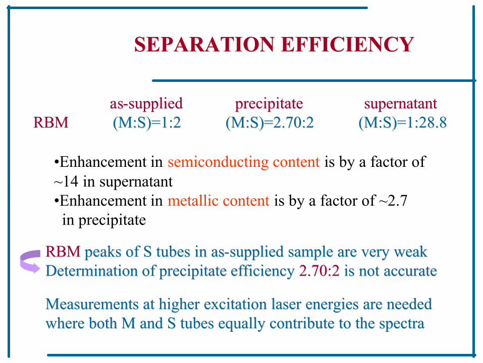
SEPARATION EFFICIENCYSEPARATION EFFICIENCY
asas--suppliedsupplied precipitateprecipitate supernatantsupernatantRBM RBM (M:S)=1:2 (M:S)=2.70:2 (M:S)=1:28.8(M:S)=1:2 (M:S)=2.70:2 (M:S)=1:28.8
RBMRBM peaks of S tubes in aspeaks of S tubes in as--supplied sample are very weaksupplied sample are very weakDetermination of precipitate efficiency Determination of precipitate efficiency 2.70:22.70:2 is not accurateis not accurate
Measurements at higher excitation laser energies are neededMeasurements at higher excitation laser energies are neededwhere both M and S tubes equally contribute to the spectrawhere both M and S tubes equally contribute to the spectra
•Enhancement in semiconducting content is by a factor of ~14 in supernatant•Enhancement in metallic content is by a factor of ~2.7 in precipitate

CONCLUDING REMARKSCONCLUDING REMARKS
• Research on nanotubes and nanowires show much interestingscience with potential for applications
• Research at present is mostly focused on demonstration stage
• Little effort has been given so far to integration into systemswith large scale production
• Synthesis control of components, integration of components and scale-up all present major challenges
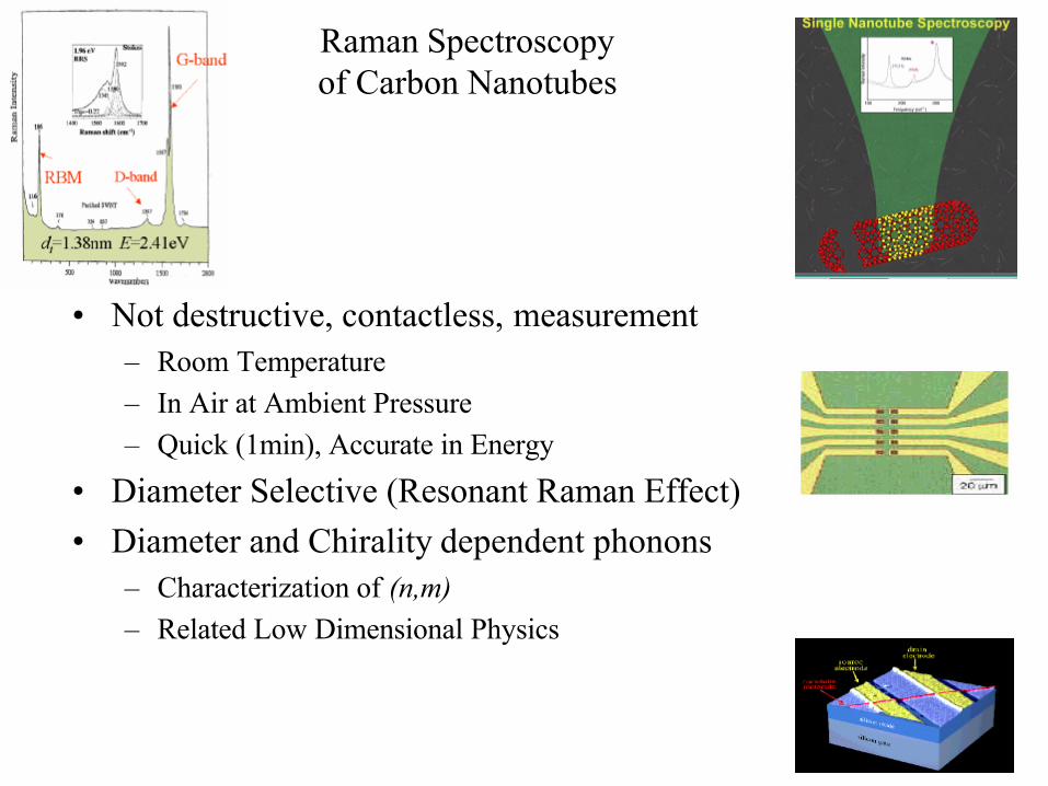
Raman Spectroscopy of Carbon Nanotubes
• Not destructive, contactless, measurement– Room Temperature– In Air at Ambient Pressure– Quick (1min), Accurate in Energy
• Diameter Selective (Resonant Raman Effect)• Diameter and Chirality dependent phonons
– Characterization of (n,m)– Related Low Dimensional Physics