overhead requirements for stateful memristor logicjoseph.friedman/papers/... · 2018-12-11 ·...
TRANSCRIPT

IEEE TRANSACTIONS ON CIRCUITS AND SYSTEMS–I: REGULAR PAPERS, VOL. 66, NO. 1, JANUARY 2019 263
Overhead Requirements for StatefulMemristor Logic
Xuan Hu , Student Member, IEEE, Michael J. Schultis, Matthew Kramer, Archit Bagla,
Akshay Shetty, and Joseph S. Friedman , Member, IEEE
Abstract— Memristors are being explored as a potentialtechnology to replace CMOS for logic-in-memory systemsthat exploit the memristive non-volatility. Memristors aretwo-terminal, non-volatile device that exhibit a variable resistancethat is dependent on the applied voltage history of the device,providing the capability to store and process information withinthe same structure. The ability of memristors to perform logichas been previously demonstrated, but previous analyses ofmemristor logic efficiency have not included the overhead CMOScircuitry that is required to control memristor logic operations.In this paper, the required overhead CMOS circuitry for imple-menting logic with memristors is evaluated for standard logicgates and a one-bit full adder to enable an analysis of the overallsystem efficiency. The results show that the number of CMOSdevices in the overhead circuitry can be upwards of 50 times thatof a conventional CMOS implementation, and that the power-delay product of the memristor logic with overhead circuitry isroughly one billion times greater than for conventional CMOScircuits. These results enable the conclusion that the overheadcircuit requirements for stateful memristor logic threaten tonegate any efficiency improvements that are achieved by thememristors themselves.
Index Terms— Memristors, memristive systems, logic gates,non-volatile logic computing, control circuit, beyond CMOScomputing, memristor control circuit.
I. INTRODUCTION
S INCE the invention of the first integrated circuit, thedensity of transistors has grown exponentially. While
this trend persists, thanks to continued advancements insilicon process technologies, many have posited that the endof Moore’s Law is quickly approaching [1]. This eventualbarrier to further increases in transistor density encouragesinvestigation into novel circuit architectures. Many conceptsfor beyond-CMOS computing have been proposed [2]–[15],with significant recent interest toward performing logic-in-memory [16], [17] with memristors [18], [19].
Based on research from HP Labs, a simplified understandingof memristor [20] behavior is depicted in Fig. 1(a), wherethe shifting of the connection points is influenced by the
Manuscript received January 16, 2018; revised May 23, 2018 andJuly 9, 2018; accepted July 20, 2018. Date of publication August 27, 2018;date of current version December 6, 2018. This paper was recommended byAssociate Editor W. Zhao. (Xuan Hu and Michael J. Schultis contributedequally to this work.) (Corresponding author: Joseph S. Friedman.)
The authors are with the Department of Electrical and Computer Engineer-ing, The University of Texas at Dallas, Richardson, TX 75080 USA (e-mail:[email protected]).
Color versions of one or more of the figures in this paper are availableonline at http://ieeexplore.ieee.org.
Digital Object Identifier 10.1109/TCSI.2018.2861463
Fig. 1. (a) Simplified memristor behavior (adapted from [21]). (b) Memristorsymbol.
applied voltage [21]. As a varying voltage is applied betweenterminals 1 and 2, the resistance of the device shifts betweenlow and high resistance states. Fig. 1(b) shows the symbol thatis commonly used for memristor devices. Consistent with thememristor model used in this work [22], a negative voltageapplied from the “+” terminal to the “−” terminal decreasesthe resistance to RON (i.e.. A positive voltage applied fromthe “+” terminal to the “−” terminal increases the resistanceto ROFF (i.e., an open circuit). Memristors based on thisbehavior have been proven to be able to perform logic boththeoretically [18] and experimentally [19], [21].
Since the publication of the work performed by HP Labs,there has been a flurry of research in this field. Thisincludes the ability of two memristors to perform the impli-cation (IMPLY) function [19], standard functions such asAND and OR [23], and more advanced functions such as theone-bit full adder [24] and multi-bit full adder [18]. Variousschemes for memristor connectivity have also been suggestedincluding the parallel [19], [25] memristor and crossbar config-urations [26]–[28]. Furthermore, some drawbacks have beenidentified, such as the potential for sneak-paths in crossbararrays [18], [29] and the need for sense amplifiers to read thestate of a memristor [18].
Amidst all of the excitement toward memristors for non-volatile logic, very serious concerns have been overlookedand minimized. In particular, the peripheral circuitry required
1549-8328 © 2018 IEEE. Personal use is permitted, but republication/redistribution requires IEEE permission.See http://www.ieee.org/publications_standards/publications/rights/index.html for more information.

264 IEEE TRANSACTIONS ON CIRCUITS AND SYSTEMS–I: REGULAR PAPERS, VOL. 66, NO. 1, JANUARY 2019
Fig. 2. Ideal thresholded memristor zero-crossing hysteresis curve.
to control memristor logic has not been fully designed andanalyzed [30]. The required CMOS control circuitry posesa serious threat that must be considered in order to enablerealistic predictions of the efficiency of this technology.
To truly understand the efficacy of a memristor-basedcomputing system, it is necessary to determine the overheadrequired to control the application of voltages to the mem-ristors. This paper therefore evaluates the CMOS circuitryrequired as overhead to control memristor-based functions,providing insight into the true viability of stateful memristorlogic. A complete overhead circuit is proposed and analyzed,leading to the conclusion that even if the memristors them-selves are ignored, more CMOS transistors are required forthe memristor control circuit than are required for a conven-tional CMOS implementation. Furthermore, the power delayproduct of a conventional CMOS implementation is greaterthan one billion times better than with memristors, provingthat even with significant improvements in memristor-basedarchitectures, CMOS-based computing is more efficient thanmemristor logic.
II. OVERVIEW OF MEMRISTOR LOGIC
To provide insight into the operation of memristors froma physical perspective, memristor technology is introduced.The IMPLY function is explained as the basis for computingwith memristors. Additional Boolean functions are consideredfor implementation with memristors, and it is shown that ifthe control circuit is ignored, fewer memristors are requiredas compared to the number of transistors in a conventionalCMOS implementation. (In Section III, it is shown that whenthe control circuit is not ignored, memristor logic requiresmany additional devices).
A. Memristor Technology
While there are many types of memristors, the most com-mon has a zero-crossing curve with hysteresis [21], [31]–[33].In the ideal I-V curve shown in Fig. 2, the device changesto a low resistance state when the voltage applied acrossthe device (VSET) is less than the VTHN voltage. Conversely,the device reverts to the high resistance state when thevoltage applied across the device (VRESET) is greater than the
Fig. 3. Bipolar filametary switching process (adapted from [36], [37]).
Fig. 4. Stateful memristor logic operation for implication function A → B .
VTHP voltage. The conditional voltage, VCOND, is also criticalto logic operation using memristors and is described in thenext section.
The physical realization of memristors varies based on thespecific construction of the memristor, and different mech-anisms have been discussed previously [34], [35]. As anintroduction, the discussion here is limited to the bipolar fil-amentary switching process. A simplified diagram is depictedin Fig. 3 to illustrate the mechanism of resistance change inthe device [36], [37]. When the VSET voltage is applied to thedevice, a metallic filament is formed, switching the device tothe low resistance state (logic “1”). When the VRESET voltageis applied to the device, the filament retreats, switching thedevice back into the high resistance state (logic “0”). Thisproperty can be exploited to perform logical operations suchas the implication function, as depicted in Fig. 4 and describedfurther in Section II.B.
As the device switching is “mechanical” in the sense thations are required to move to form a filament, the switchingspeed is limited by the velocity of the ions. Though theswitching speed may be limited, the mechanical switchingenables these devices to retain their state without externalexcitation. This quality makes memristors a promising tech-nology, as they can both perform logical functions as wellas act as local memory storage, reducing long-distance datatransfer and overcoming the von Neumann bottleneck [34].This non-volatile memristor device can be used both to storeinformation as well as perform complex logic functions [18],[19], [23], [24], with the implication function as the basis formemristor logic.

HU et al.: OVERHEAD REQUIREMENTS FOR STATEFUL MEMRISTOR LOGIC 265
TABLE I
IMPLY FUNCTION TRUTH TABLE AND NODE VOLTAGES
Fig. 5. Implication logic operation for case 3 of Table I.
B. Implication Function
The IMPLY gate is the fundamental building block forstateful memristor logic. The IMPLY function is commonlydenoted by → or IMP (e.g., A → B or A IMP B), and isalso known as the material conditional [19]. The A IMP Bfunction can also be understood as standard Boolean logicfunction NOT(A) OR B (i.e. A + B). This function is notcommutative, and the four input cases are shown in the truthtable of Table I. The inputs of the IMPLY function are thestates of the memristors A and B, and the output is the stateof B after the operation (B’). The state of memristor A isunchanged during the IMPLY operation.
Fig. 5 depicts the functional operation of the IMPLY gatefor case 3, illustrating the importance of the VCOND voltage.As described in Fig. 2, the memristor switches states fromhigh resistance (0) to low resistance (1) when the VSETvoltage is applied across its terminals from + to −. TheVCOND voltage is of less magnitude than VSET, such thatapplying VCOND or (VSET - VCOND) does not change thememristor from high resistance (0) to low resistance (1).Table I summarizes each of the four combinations of inputs forthe IMPLY gate, noting the voltages applied and the states ofeach of the memristors before, during, and after the operation.
C. Stateful Memristor Logic
The IMPLY gate can be extended to perform additionallogic functions with the addition of parallel memristors. It hasbeen shown in [19] that a NAND operation can be performed,and in [18] that the AND, OR, NOR, and XOR gates can beimplemented with serial applications of the implication func-tion. Beyond the advantage of non-volatility in memristors,an additional benefit to memristors is that fewer devices arerequired to perform standard logic functions (when the control
TABLE II
FUNCTION DEVICE COUNT WITHOUT CONTROL CIRCUITRY
overhead is not included). Table II summarizes the number oftransistors required compared to the number of memristorsrequired for equivalent functions.
Table II shows that memristors have a clear advantageover standard CMOS when considering the number of devicesrequired to perform the logical function itself. When usingmemristors, the standard Boolean functions may require onlyone-third as many the number of devices required for CMOS,and the full adder circuit requires 22 fewer devices, a nearly80% reduction. However, this comparison only tells part ofthe story.
A significant drawback to the six-memristor full adderimplementation is that the function requires 29 serial steps,signficantly slowing down the operation time [18]. In addi-tion to the significant reduction in operating speed due tothe mechanical switching of memristors and the number ofserial steps, this device comparison does not fully considerall circuitry required. While it has been shown that theseBoolean functions can be performed using fewer memristors(as compared to transistors) when the overhead circuit isignored, little research has gone into fully understanding therequired supporting CMOS circuitry necessary to coordinatesequential operations in memristor-based logic arrays.
D. Alternative Memristor Logic Styles
This paper focuses specifically on the IMPLY-based logicof [18], [19], and [25]. Many other memristor logic styles havebeen proposed, including:
• Memristor ratioed logic (MRL) [38],• Memristor-aided logic (MAGIC) [39],• Complementary resistive switch (CRS) logic [40], [41],• Crossbar array logic [42], and• Memristors-as-drivers (MAD) logic [43], [44].
The voltages applied to the memristors must be carefullycoordinated by non-memristor devices presumably CMOStransistors in all of these configurations. Therefore, the chal-lenges identified in this paper may extend to other memristorlogic styles.
III. OVERHEAD CIRCUITRY FOR BOOLEAN FUNCTIONS
As noted above, the design of peripheral circuitry for mem-ristor logic has not been previously proposed [30]. To evaluate
266 IEEE TRANSACTIONS ON CIRCUITS AND SYSTEMS–I: REGULAR PAPERS, VOL. 66, NO. 1, JANUARY 2019
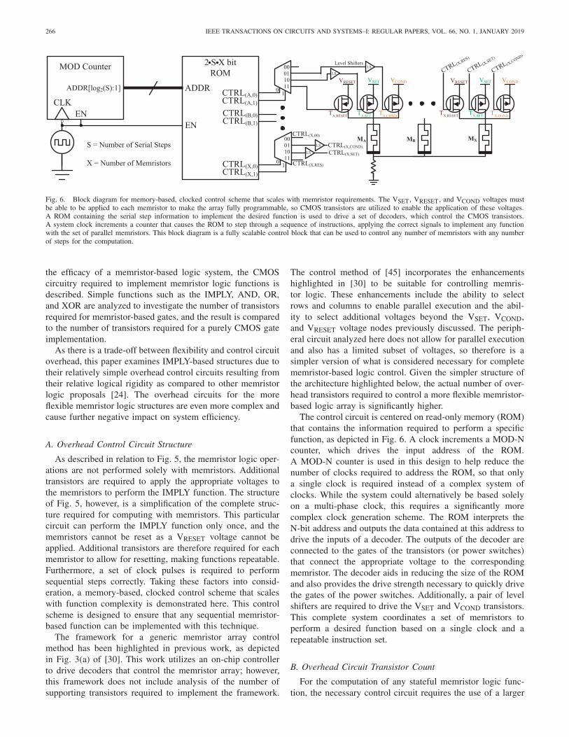
Fig. 6. Block diagram for memory-based, clocked control scheme that scales with memristor requirements. The VSET, VRESET, and VCOND voltages mustbe able to be applied to each memristor to make the array fully programmable, so CMOS transistors are utilized to enable the application of these voltages.A ROM containing the serial step information to implement the desired function is used to drive a set of decoders, which control the CMOS transistors.A system clock increments a counter that causes the ROM to step through a sequence of instructions, applying the correct signals to implement any functionwith the set of parallel memristors. This block diagram is a fully scalable control block that can be used to control any number of memristors with any numberof steps for the computation.
the efficacy of a memristor-based logic system, the CMOScircuitry required to implement memristor logic functions isdescribed. Simple functions such as the IMPLY, AND, OR,and XOR are analyzed to investigate the number of transistorsrequired for memristor-based gates, and the result is comparedto the number of transistors required for a purely CMOS gateimplementation.
As there is a trade-off between flexibility and control circuitoverhead, this paper examines IMPLY-based structures due totheir relatively simple overhead control circuits resulting fromtheir relative logical rigidity as compared to other memristorlogic proposals [24]. The overhead circuits for the moreflexible memristor logic structures are even more complex andcause further negative impact on system efficiency.
A. Overhead Control Circuit Structure
As described in relation to Fig. 5, the memristor logic oper-ations are not performed solely with memristors. Additionaltransistors are required to apply the appropriate voltages tothe memristors to perform the IMPLY function. The structureof Fig. 5, however, is a simplification of the complete struc-ture required for computing with memristors. This particularcircuit can perform the IMPLY function only once, and thememristors cannot be reset as a VRESET voltage cannot beapplied. Additional transistors are therefore required for eachmemristor to allow for resetting, making functions repeatable.Furthermore, a set of clock pulses is required to performsequential steps correctly. Taking these factors into consid-eration, a memory-based, clocked control scheme that scaleswith function complexity is demonstrated here. This controlscheme is designed to ensure that any sequential memristor-based function can be implemented with this technique.
The framework for a generic memristor array controlmethod has been highlighted in previous work, as depictedin Fig. 3(a) of [30]. This work utilizes an on-chip controllerto drive decoders that control the memristor array; however,this framework does not include analysis of the number ofsupporting transistors required to implement the framework.
The control method of [45] incorporates the enhancementshighlighted in [30] to be suitable for controlling memris-tor logic. These enhancements include the ability to selectrows and columns to enable parallel execution and the abil-ity to select additional voltages beyond the VSET, VCOND,and VRESET voltage nodes previously discussed. The periph-eral circuit analyzed here does not allow for parallel executionand also has a limited subset of voltages, so therefore is asimpler version of what is considered necessary for completememristor-based logic control. Given the simpler structure ofthe architecture highlighted below, the actual number of over-head transistors required to control a more flexible memristor-based logic array is significantly higher.
The control circuit is centered on read-only memory (ROM)that contains the information required to perform a specificfunction, as depicted in Fig. 6. A clock increments a MOD-Ncounter, which drives the input address of the ROM.A MOD-N counter is used in this design to help reduce thenumber of clocks required to address the ROM, so that onlya single clock is required instead of a complex system ofclocks. While the system could alternatively be based solelyon a multi-phase clock, this requires a significantly morecomplex clock generation scheme. The ROM interprets theN-bit address and outputs the data contained at this address todrive the inputs of a decoder. The outputs of the decoder areconnected to the gates of the transistors (or power switches)that connect the appropriate voltage to the correspondingmemristor. The decoder aids in reducing the size of the ROMand also provides the drive strength necessary to quickly drivethe gates of the power switches. Additionally, a pair of levelshifters are required to drive the VSET and VCOND transistors.This complete system coordinates a set of memristors toperform a desired function based on a single clock and arepeatable instruction set.
B. Overhead Circuit Transistor Count
For the computation of any stateful memristor logic func-tion, the necessary control circuit requires the use of a larger

HU et al.: OVERHEAD REQUIREMENTS FOR STATEFUL MEMRISTOR LOGIC 267
number of transistors than is required for a conventionalCMOS implementation. The conventional CMOS NAND andNOR functions require only four transistors; the statefulmemristor logic control circuit requires a larger number oftransistors for the control circuit consisting of a counter, read-only memory (ROM), a decoder, level shifters, and drivers.This is mathematically proven below; optimizations are madefor stateful memristor logic systems with a large number ofsteps, as it is readily apparent that stateful memristor logicsystems with a small number of steps require more transistorsthan conventional CMOS.
The static counter used in this work utilizes 28 transistorsper counter stage. As the number of stages is equivalent tolog2(S) for a stateful memristor logic function with S steps,the number of transistors required by the counter is
NCOUNT = 28log2(S). (1)
In a system with a large number of sequential steps, the tran-sistor cost of the counter is less significant than in a smallsystem.
The sequential operations inherent to stateful memristorlogic requires ROMs to store the operation codes that setthe memristor driving circuits to the desired modes. For eachmemristor at each time step, two bits of information arerequired to encode the voltage applied to the memristor amongthe four possibilities: floating, conditional, set, and reset.Therefore, a two-bit ROM is required for each memristor ateach time step. The minimum core ROM size for any particularfunction is therefore
NROM,CORE = 2X S, (2)
where X is the number of memristors required for thatfunction. Additionally, an X-row ROM utilizes a log2(X)-bitaddress signal, which requires a log2(X)-to-X decoder for theROM word lines. Furthermore, an S-column ROM requiresS pre-charge PMOS transistors to pull-up the bit line and asense amplifier to read-out the bit stored in the ROM. A five-transistor differential amplifier is the simplest sense amplifierstructure, though most practical sense amplifiers consist of alarger number of transistors. For a ROM with X rows andS columns, the peripheral circuits therefore require at least
NROM,PERIPHERAL = 6X + 6S − 2 (3)
transistors. The total number of transistors required by theROM is therefore at least
NROM = NROM,CORE + NROM,PERIPHERAL
= 2X S + 6X + 6S − 2. (4)
While the other components of the control circuit add signif-icantly to the overhead cost, the transistor count of this ROMalone is greater than a conventional CMOS logic circuit and isa fundamental cause of the inefficiency of stateful memristorlogic.
In order to minimize the size of the ROM of a function thatrequires many steps (as in any large-scale system), the two-bitencoding described above is used to represent the four voltagelevels applied to each memristor rather than four bits as would
be required by a naïve design. It is therefore necessary to use2:4 decoders for each memristor, at a cost of 22 transistorseach, for a total of
NDEC = 22X. (5)
If instead the ROM signals are directly used as the inputs todriving circuits without encoding, the required ROM size isdoubled to
NROM,NoDecoder = 4X S + 12X + 6S − 2. (6)
Therefore, decoders are used in this analysis.As negative voltages are used for the implication opera-
tion, voltage level shifters are required to deliver both theVCond and VSet voltages to each memristor. Each level shifterrequires ten transistors, for a total transistor count of
NLS = 2(10X) = 20X. (7)
Finally, driver transistors are required to connect each ofthe three possible memristor voltages (VCond, VSet, and VReset)to the supply rails. While these transistors must be relativelylarge, only one transistor is required for each of these voltagesfor each memristor, for a transistor count of
NDRIVE = 3X. (8)
The total transistor count of the stateful memristor logiccontrol circuit is given by
NTOTAL = NCOUNT + NROM + NDEC + NLS + NDRIVE
= 28log2(S) + 2X S + 51X + 6S – 2. (9)
Therefore, for additional sequential steps with a given numberof memristors, each memristor requires the following numberof transistors:
NSTEP = 28log2(S) + 2X S + 6S. (10)
Therefore, as an implication operation requires one step withtwo memristors, the cost of one implication operation is atleast ten CMOS transistors. (This assumes that the countersize is not increased and that all necessary memristors and thecorresponding CMOS control circuitry are already included inthe system and can be directly used for computation.) As thesimplest two-input logic functions (NOR and NAND) requirefour transistors in a conventional CMOS implementation,the number of transistors in the stateful memristor logic controlcircuit is always larger than a conventional CMOS logiccircuit.
C. CMOS Requirements for Boolean Functions
Only two memristors and a single step are required toperform the IMPLY operation. However, the ROM requires14 transistors, the decoder requires 44 transistors, the levelshifters require 40 transistors, and there are six control tran-sistors, totaling 104 supporting transistors which is nearly20 times the amount required to perform the same functionin traditional CMOS. This result includes ROM optimizationsand scales up with the number of memristors and instruc-tions required, making this additional overhead burdensome.

268 IEEE TRANSACTIONS ON CIRCUITS AND SYSTEMS–I: REGULAR PAPERS, VOL. 66, NO. 1, JANUARY 2019
TABLE III
NUMBER OF DEVICES REQUIRED TO PERFORM STANDARD FUNCTIONSWITH SUPPORTING TRANSISTOR COUNT FOR MEMRISTORS
As shown in Table III, the IMPLY function requires fewerdevices as compared to standard CMOS; however, when thesupporting CMOS structure for memristor logic is considered,the IMPLY gate requires many additional transistors.
With the structure in Fig. 6, it is clear that a large numberof additional CMOS transistors are required for operatinga scalable memristor-based computation. The same controlmethod is used to evaluate the number of transistors requiredfor other standard Boolean functions including NAND, AND,NOR, OR, XOR, and XNOR. Each structure scales up withthe number of steps required in addition to the number ofmemristors. Table III summarizes the number of memristorsand additional transistors required for the memristor architec-ture relative to the number of transistors required for a pureCMOS implementation.
A simple NAND gate that typically only requires4 transistors in a pure CMOS implementation requires231 additional transistors when computing the function uti-lizing three memristors. It is clear from the table that alarge supporting structure is required for computing withmemristors, which can be a major barrier to using memristorsto perform logic; even with significant potential improvements,the overhead requirements remain overwhelming.
IV. NAND AND FULL ADDER OVERHEAD ANALYSIS
To demonstrate the challenges resulting from the overheadcircuitry, memristor NAND and full adder circuits are thor-oughly analyzed. The simulation modeling methods, circuitdesign, and simulation results are provided, and the overheadcircuitry is compared to a standard CMOS implementation.Additionally, the power-delay product, a metric of the effi-ciency of a logic system, is analyzed for memristor-based logicand compared to a CMOS implementation.
A. Simulation Approach
In this work, the VTEAM memristor model [22] is usedto simulate the memristors in the circuit. The IBM 130 nmCMOS technology is integrated with the VTEAM model todesign and simulate the CMOS overhead circuit, as well as forthe conventional CMOS implementation. The ROM is simu-lated in a behavioral manner and does not impact the electrical
TABLE IV
MEMRISTOR NAND FUNCTIONAL SEQUENCE
TABLE V
VTEAM MODEL PARAMETERS
simulation results; the overhead circuit performance and effi-ciency should therefore be considered optimistic. The VTEAMmemristor model, described in Table IV [22], provides athreshold of −0.85 V for switching from high resistance tolow resistance; in other words, a negative voltage appliedto the positive terminal of the device reduces the resistance.The VTEAM memristor model has a threshold of 0.22 V forswitching from low resistance back to high resistance; that is,a positive voltage greater than 0.22 V increases the resistance.While the model utilized here is not a representative exampleof the fastest memristors demonstrated to date [46], the gapin efficiency shown in section IV.D demonstrates that thesefabrication improvements are inconsequential.
B. Memristor NAND Operation With Overhead Circuit
Similar to CMOS, the NAND gate implementation is thesimplest standard Boolean logic function that can be per-formed with memristors. The NAND gate implementation hereis adapted from [19] and requires only three memristors andtwo steps. As shown in Table V, the IMPLY function ispeformed between each of the input devices and the outputdevice sequentially. As noted previously in Table I, if the inputmemristor is in the high resistance state (0), the output mem-ristor will switch from high resistance (0) to low resistance (1).For the NAND function, if either input memristors is in thehigh resistance state (0), then the output memristor will switchto the low resistance state (1). On the other hand, if both inputsare in the low resistance state (1), then the output will remainin the high resistance state (0), thereby performing the NANDfunction.
The result of the A = B = 0 input combination for theNAND gate simulation is depicted in Fig. 7, where both inputsstart in the high resistance state (0). The power switch control

HU et al.: OVERHEAD REQUIREMENTS FOR STATEFUL MEMRISTOR LOGIC 269
Fig. 7. Simulation of memristor NAND gate. Three memristors MA, MB, and MY perform the function MA NAND MB where memristor MY contains theoutput of the operation. The clock pulse triggers an update of the ROM address on the falling edge and enables the ROM and decoder when high. The ROMaddress and the input signals to each of the decoders are displayed, in accordance with the structure of Fig. 6. Each memristor has three control transistorsfor applying VCOND, VSET, and VRESET. The voltage of the control signals for each of the nine transistors and the resulting states of the three memristorsis shown, where a high signal in the waveform corresponds to turning on the switch that applies VCOND, VSET, or VRESET to the A, B, or Y memristor.The analog voltage across each of the memristors illustrates how each of the memristors changes states based on the VTHP and VTHN threshold voltages.At the end of the simulation, the state of each of the memristors exhibits the correct calculation of the function.
signals are shown for all nine transistors to illustrate how eachof the voltages are applied to the corresponding memristor.The first step depicts how the output device, MY, is set to 0by turning on the TY,RESET transistor. The second step is abuffer step to ensure the output device is reset properly dueto the slow switching speed of the memristor. Steps threeand four show how the TA,COND and TB,COND transistors areenabled for the input devices, MA and MB, and the TY,SETtransistor is enabled for the output device, MY, to performthe implication function as described previously in Fig. 5 andTable II. It can be seen from Fig. 7 that during the first IMPLYstep, MA → MY, the output switches from the high resistancestate (0) to the low resistance state (1). The second IMPLYstep, MB → MY also can change the output from the highresistance state (0) to the low resistance state (1), however,in this example the state already changed during the first step,so the output remains in the low resistance state (1). Thecorrect result of the NAND gate is shown at the end of thesimulation, with the output in the low resistance state (1).
As mentioned previously, the memristor undergoes astate change through the motion of ions, which can be a
slow process. Note the long delay in Fig. 7 for the memristorto switch states, in addition to the slow speed of the entirefunction. The device requires between 2 and 3 µs to switch,and the entire function requires nearly 20 µs to perform,as compared to a standard CMOS implementation that isachieved within nanoseconds. Even if the model utilized asignificantly faster memristor, it would still be much slowerthan a CMOS transistor.
C. Memristor One-Bit Full Adder With Overhead Circuit
A more thorough analysis of the overhead circuit require-ments is achieved through the design and simulation of amemristor one-bit full adder and the corresponding overhead.The memristor one-bit full-adder function is adapted fromKvatinksy et al. [18], which uses a six memristor structure toperform the function in 29 serial steps. The memristor circuitis depicted in Fig. 9, utilizing the overhead structure describedpreviously in Fig. 6.
The simulation results are depicted in Fig. 8, showingthe evolution of the memristor states through the 29 steps.

270 IEEE TRANSACTIONS ON CIRCUITS AND SYSTEMS–I: REGULAR PAPERS, VOL. 66, NO. 1, JANUARY 2019
Fig. 8. Simulation of the one-bit full adder using memristors. Six memristors A, B, Carry, M1, M2, and Sum are utilized to perform the function where A,B, and Carry are the inputs and Carry and Sum are the outputs. Each memristor is driven by three transistors for applying VCOND, VSET, and VRESET,with the gate voltages not shown here. The states for each of the six memristors are shown throughout the entire calculation. Each set of steps highlights asub-function that is utilized in the sequence to calculate the final Cout and Sum. This set of steps is adapted from [4] to perform the one-bit full adder withthe fewest memristors.
Fig. 9. Memristor structure for implementing a one-bit full adder based onthe serial step method provided in [18].
The most complex case of the one-bit full adder is used,where A, B, and Cin all begin in the low resistance state (1).The standard logic functions of which the full adder is com-prised are separated and highlighted. Overall, the simulationtakes 34 steps rather than 29 steps, as buffer steps are requiredwhenever a Reset operation is performed. The results demon-strate proper functionality with the Cout and Sum ultimatelyin the low resistance state (1).
The memristor one-bit full adder requires 427 supportingtransistors, 14 times more than the number of transistorsrequired for a standard CMOS implementation. Even if the
control circuitry were further optimized, the system would stillrequire many more transistors than required in a pure CMOSimplementation. In addition to the large overhead required,the 34 serial steps required to implement this function withonly six memristors results in a calculation time of 200 µs.While memristors can perform logic-in-memory, the increasein the delay for performing even simple calculations is farmore problematic than the delay resulting from the vonNeumann bottleneck. Even if the true devices and simulationwere significantly faster, a CMOS implementation would stillbe multiple orders of magnitude faster than a memristor-basedsolution.
D. Analysis Of Power-Delay Product
As highlighted previously, the state-change operation ofmemristors require both a significant amount of power con-sumption, due to the current required to mobilize the ions,and time, due to the mechanical switching and number ofserial steps. A standard figure of merit, the power-delayproduct (PDP), is measured in simulation and compared toa standard CMOS implementation. The PDP is measured forboth the memristor logic and the CMOS logic by measuringthe current through each device and calculating the energy
HU et al.: OVERHEAD REQUIREMENTS FOR STATEFUL MEMRISTOR LOGIC 271
TABLE VI
POWER-DELAY PRODUCT FOR MEMRISTORS AND CMOS
TABLE VII
ENERGY-DELAY PRODUCT FOR MEMRISTORS AND CMOS
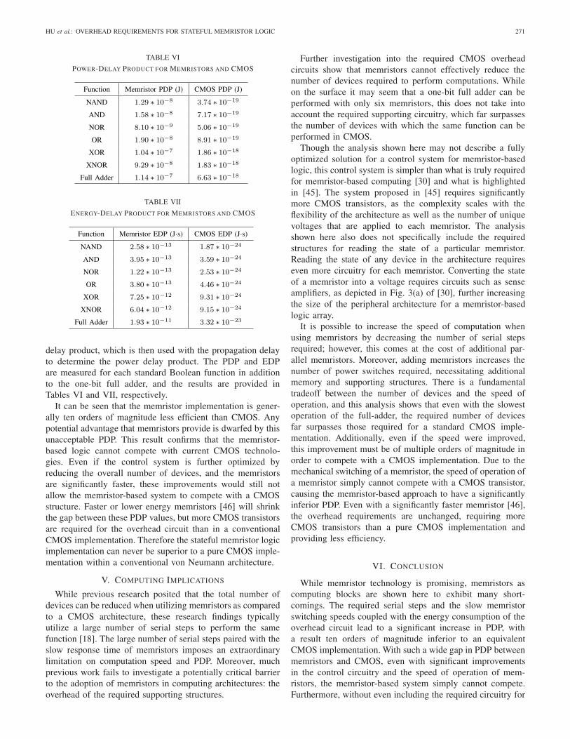
delay product, which is then used with the propagation delayto determine the power delay product. The PDP and EDPare measured for each standard Boolean function in additionto the one-bit full adder, and the results are provided inTables VI and VII, respectively.
It can be seen that the memristor implementation is gener-ally ten orders of magnitude less efficient than CMOS. Anypotential advantage that memristors provide is dwarfed by thisunacceptable PDP. This result confirms that the memristor-based logic cannot compete with current CMOS technolo-gies. Even if the control system is further optimized byreducing the overall number of devices, and the memristorsare significantly faster, these improvements would still notallow the memristor-based system to compete with a CMOSstructure. Faster or lower energy memristors [46] will shrinkthe gap between these PDP values, but more CMOS transistorsare required for the overhead circuit than in a conventionalCMOS implementation. Therefore the stateful memristor logicimplementation can never be superior to a pure CMOS imple-mentation within a conventional von Neumann architecture.
V. COMPUTING IMPLICATIONS
While previous research posited that the total number ofdevices can be reduced when utilizing memristors as comparedto a CMOS architecture, these research findings typicallyutilize a large number of serial steps to perform the samefunction [18]. The large number of serial steps paired with theslow response time of memristors imposes an extraordinarylimitation on computation speed and PDP. Moreover, muchprevious work fails to investigate a potentially critical barrierto the adoption of memristors in computing architectures: theoverhead of the required supporting structures.
Further investigation into the required CMOS overheadcircuits show that memristors cannot effectively reduce thenumber of devices required to perform computations. Whileon the surface it may seem that a one-bit full adder can beperformed with only six memristors, this does not take intoaccount the required supporting circuitry, which far surpassesthe number of devices with which the same function can beperformed in CMOS.
Though the analysis shown here may not describe a fullyoptimized solution for a control system for memristor-basedlogic, this control system is simpler than what is truly requiredfor memristor-based computing [30] and what is highlightedin [45]. The system proposed in [45] requires significantlymore CMOS transistors, as the complexity scales with theflexibility of the architecture as well as the number of uniquevoltages that are applied to each memristor. The analysisshown here also does not specifically include the requiredstructures for reading the state of a particular memristor.Reading the state of any device in the architecture requireseven more circuitry for each memristor. Converting the stateof a memristor into a voltage requires circuits such as senseamplifiers, as depicted in Fig. 3(a) of [30], further increasingthe size of the peripheral architecture for a memristor-basedlogic array.
It is possible to increase the speed of computation whenusing memristors by decreasing the number of serial stepsrequired; however, this comes at the cost of additional par-allel memristors. Moreover, adding memristors increases thenumber of power switches required, necessitating additionalmemory and supporting structures. There is a fundamentaltradeoff between the number of devices and the speed ofoperation, and this analysis shows that even with the slowestoperation of the full-adder, the required number of devicesfar surpasses those required for a standard CMOS imple-mentation. Additionally, even if the speed were improved,this improvement must be of multiple orders of magnitude inorder to compete with a CMOS implementation. Due to themechanical switching of a memristor, the speed of operation ofa memristor simply cannot compete with a CMOS transistor,causing the memristor-based approach to have a significantlyinferior PDP. Even with a significantly faster memristor [46],the overhead requirements are unchanged, requiring moreCMOS transistors than a pure CMOS implementation andproviding less efficiency.
VI. CONCLUSION
While memristor technology is promising, memristors ascomputing blocks are shown here to exhibit many short-comings. The required serial steps and the slow memristorswitching speeds coupled with the energy consumption of theoverhead circuit lead to a significant increase in PDP, witha result ten orders of magnitude inferior to an equivalentCMOS implementation. With such a wide gap in PDP betweenmemristors and CMOS, even with significant improvementsin the control circuitry and the speed of operation of mem-ristors, the memristor-based system simply cannot compete.Furthermore, without even including the required circuitry for

272 IEEE TRANSACTIONS ON CIRCUITS AND SYSTEMS–I: REGULAR PAPERS, VOL. 66, NO. 1, JANUARY 2019
reading the state of the memristors, it has been determinedthat the number of supporting transistors can be upwardsof 50 times the number of transistors required for a standardCMOS implementation. Therefore, though stateful memristorlogic may have utility within a non-von Neumann computingarchitecture that makes efficient use of the memristor non-volatility, the prospects for stateful memristor logic within aconventional computer architecture are severely limited by theoverhead circuit requirements.
ACKNOWLEDGMENT
The authors would like to thank M. Rathna, Y. Liu,P. X. Francis, E. Linn, A. Siemon, S. Menzel, and S. Kvatinksyfor their contributions toward this paper.
REFERENCES
[1] D. J. Frank, R. H. Dennard, E. Nowak, P. M. Solomon, Y. Taur,and H. S. P. Wong, “Device scaling limits of Si MOSFETs and theirapplication dependencies,” Proc. IEEE, vol. 89, no. 3, pp. 259–287,Mar. 2001.
[2] S. Matsunaga et al., “Fabrication of a nonvolatile full adder based onlogic-in-memory architecture using magnetic tunnel junctions,” Appl.Phys. Express, vol. 1, no. 9, p. 091301, Aug. 2008.
[3] M. T. Niemier et al., “Nanomagnet logic: Progress toward system-levelintegration,” J. Phys., Condens. Matter, vol. 23, no. 49, p. 493202,Nov. 2011.
[4] K. A. Omari and T. J. Hayward, “Chirality-based vortex domain-walllogic gates,” Phys. Rev. Appl., vol. 2, no. 4, p. 044001, Oct. 2014.
[5] J. S. Friedman, B. W. Wessels, G. Memik, and A. V. Sahakian, “Emitter-coupled spin-transistor logic: Cascaded spintronic computing beyond10 GHz,” IEEE J. Emerg. Sel. Topics Circuits Syst., vol. 5, no. 1,pp. 17–27, Mar. 2015.
[6] D. A. Allwood, G. Xiong, C. C. Faulkner, D. Atkinson, D. Petit,and R. P. Cowburn, “Magnetic domain-wall logic,” Science, vol. 309,pp. 1688–1692, Sep. 2005.
[7] A. Imre, G. Csaba, L. Ji, A. Orlov, G. H. Bernstein, and W. Porod,“Majority logic gate for magnetic quantum-dot cellular automata,”Science, vol. 311, no. 5758, pp. 205–208, 2006.
[8] J. A. Currivan, Y. Jang, M. D. Mascaro, M. A. Baldo, and C. A. Ross,“Low energy magnetic domain wall logic in short, narrow, ferromagneticwires,” IEEE Magn. Lett., vol. 3, Apr. 2012, Art. no. 3000104.
[9] J. S. Friedman and A. V. Sahakian, “Complementary magnetic tun-nel junction logic,” IEEE Trans. Electron Devices, vol. 61, no. 4,pp. 1207–1210, Apr. 2014.
[10] J. S. Friedman et al., “Cascaded spintronic logic with low-dimensionalcarbon,” Nature Commun., vol. 8, Jun. 2017, Art. no. 15635.
[11] J. S. Friedman, A. Godkin, A. Henning, Y. Vaknin, Y. Rosenwaks,and A. V. Sahakian, “Threshold logic with electrostaticallyformed nanowires,” IEEE Trans. Electron Devices, vol. 63, no. 3,pp. 1388–1391, Mar. 2016.
[12] Y.-M. Lin, J. Appenzeller, J. Knoch, and P. Avouris, “High-performancecarbon nanotube field-effect transistor with tunable polarities,” IEEETrans. Nanotechnol., vol. 4, no. 5, pp. 481–489, Sep. 2005.
[13] M. M. Shulaker et al., “Carbon nanotube computer,” Nature, vol. 501,no. 7468, pp. 526–530, 2013.
[14] M. H. Ben-Jamaa, K. Mohanram, and G. De Micheli, “An efficientgate library for ambipolar CNTFET logic,” IEEE Trans. Comput.-AidedDesign Integr. Circuits Syst., vol. 30, no. 2, pp. 242–255, Feb. 2011.
[15] M. Prakash and N. Gershenfeld, “Microfluidic bubble logic,” Science,vol. 315, no. 5813, pp. 832–835, Feb. 2007.
[16] W. Kang, Z. Wang, Y. Zhang, J.-O. Klein, W. Lv, and W. Zhao,“Spintronic logic design methodology based on spin Hall effect-drivenmagnetic tunnel junctions,” J. Phys. D, Appl. Phys., vol. 49, no. 6,p. 65008, 2016.
[17] H. Zhang, W. Kang, L. Wang, K. L. Wang, and W. Zhao, “Statefulreconfigurable logic via a single-voltage-gated spin Hall-effect drivenmagnetic tunnel junction in a spintronic memory,” IEEE Trans. ElectronDevices, vol. 64, no. 10, pp. 4295–4301, Oct. 2017.
[18] S. Kvatinsky, G. Satat, N. Wald, E. G. Friedman, A. Kolodny, andU. C. Weiser, “Memristor-based material implication (IMPLY) logic:Design principles and methodologies,” IEEE Trans. Very Large ScaleIntegr. (VLSI) Syst., vol. 22, no. 10, pp. 2054–2066, Oct. 2014.
[19] J. Borghetti, G. S. Snider, P. J. Kuekes, J. J. Yang, D. R. Stewart, andR. S. Williams, “‘Memristive’ switches enable ‘stateful’ logic operationsvia material implication,” Nature, vol. 464, no. 7290, pp. 873–876,Apr. 2010.
[20] L. O. Chua, “Memristor—The missing circuit element,” IEEE Trans.Circuit Theory, vol. CT-18, no. 5, pp. 507–519, Sep. 1971.
[21] D. B. Strukov, G. S. Snider, D. R. Stewart, and R. S. Williams,“The missing memristor found,” Nature, vol. 453, pp. 80–83,May 2008.
[22] S. Kvatinsky, M. Ramadan, E. G. Friedman, and A. Kolodny, “VTEAM:A general model for voltage-controlled memristors,” IEEE Trans.Circuits Syst., II, Exp. Briefs, vol. 62, no. 8, pp. 786–790, Aug. 2015.
[23] S. Balatti, S. Ambrogio, and D. Ielmini, “Normally-off logic based onresistive switches—Part I: Logic gates,” IEEE Trans. Electron Devices,vol. 62, no. 6, pp. 1831–1838, Jun. 2015.
[24] S. Balatti, S. Ambrogio, and D. Ielmini, “Normally-off logic basedon resistive switches—Part II: Logic circuits,” IEEE Trans. ElectronDevices, vol. 62, no. 6, pp. 1839–1847, Jun. 2015.
[25] E. Lehtonen and M. Laiho, “Stateful implication logic with memristors,”in Proc. IEEE/ACM NANOARCH, Jul. 2009, pp. 33–36.
[26] S. Shin, K. Kim, and S.-M. Kang, “Reconfigurable stateful nor gate forlarge-scale logic-array integrations,” IEEE Trans. Circuits Syst., II, Exp.Briefs, vol. 58, no. 7, pp. 442–446, Jul. 2011.
[27] G. Snider, “Computing with hysteretic resistor crossbars,” Appl. Phys. A,Solids Surf., vol. 80, no. 6, pp. 1165–1172, Mar. 2005.
[28] J. J. Yang, D. B. Strukov, and D. R. Stewart, “Memristive devices forcomputing,” Nature Nanotechnol., vol. 8, no. 1, pp. 13–24, 2013.
[29] Y. Cassuto, S. Kvatinsky, and E. Yaakobi, “Sneak-path constraints inmemristor crossbar arrays,” in Proc. IEEE ISIT, Jul. 2013, pp. 156–160.
[30] J. Reuben et al., “Memristive logic: A framework for evaluation andcomparison,” in Proc. IEEE PATMOS, Sep. 2017, pp. 1–8.
[31] K. Miller, K. S. Nalwa, A. Bergerud, N. M. Neihart, and S. Chaudhary,“Memristive behavior in thin anodic titania,” IEEE Electron Device Lett.,vol. 31, no. 7, pp. 737–739, Jul. 2010.
[32] Q. Xia et al., “Memristor-CMOS hybrid integrated circuits for recon-figurable logic,” Nano Lett., vol. 9, no. 10, pp. 3640–3645, 2009.
[33] I. Valov et al., “Nanobatteries in redox-based resistive switches requireextension of memristor theory,” Nature Commun., vol. 4, Apr. 2013,Art. no. 1771.
[34] H.-S. P. Wong and S. Salahuddin, “Memory leads the way to better com-puting,” Nature Nanotechnol., vol. 10, no. 3, pp. 191–194, Mar. 2015.
[35] A. H. Edwards, H. J. Barnaby, K. A. Campbell, M. N. Kozicki, W. Liu,and M. J. Marinella, “Reconfigurable memristive device technologies,”Proc. IEEE, vol. 103, no. 7, pp. 1004–1033, Jul. 2015.
[36] I. Valov and M. N. Kozicki, “Cation-based resistance change memory,”J. Phys. D, Appl. Phys., vol. 46, no. 8, p. 074005, Jan. 2013.
[37] D. J. Wouters, R. Waser, and M. Wuttig, “Phase-change and redox-based resistive switching memories,” Proc. IEEE, vol. 103, no. 8,pp. 1274–1288, Aug. 2015.
[38] S. Kvatinsky, N. Wald, G. Satat, A. Kolodny, U. C. Weiser, andE. G. Friedman, “MRL—Memristor ratioed logic,” in Proc. Int. Work-shop Cellular Nanosc. Netw. Their Appl., 2012, pp. 1–6.
[39] S. Kvatinsky et al., “MAGIC—Memristor-aided logic,” IEEE Trans.Circuits Syst., II, Exp. Briefs, vol. 61, no. 11, pp. 895–899,Nov. 2014.
[40] E. Linn, R. Rosezin, C. Kügeler, and R. Waser, “Complementaryresistive switches for passive nanocrossbar memories,” Nature Mater.,vol. 9, no. 5, pp. 403–406, May 2010.
[41] R. Rosezin, E. Linn, C. Kügeler, R. Bruchhaus, and R. Waser, “Cross-bar logic using bipolar and complementary resistive switches,” IEEEElectron Device Lett., vol. 32, no. 6, pp. 710–712, Jun. 2011.
[42] E. Linn, R. Rosezin, S. Tappertzhofen, U. Böttger, and R. Waser,“Beyond von Neumann—Logic operations in passive crossbar arraysalongside memory operations,” Nanotechnology, vol. 23, no. 30,p. 305205, 2012.
[43] L. Guckert and E. E. Swartzlander, “MAD gates—Memristor logicdesign using driver circuitry,” IEEE Trans. Circuits Syst., II, Exp. Briefs,vol. 64, no. 2, pp. 171–175, Feb. 2017.
[44] L. Guckert and E. E. Swartzlander, “Optimized memristor-based mul-tipliers,” IEEE Trans. Circuits Syst. I, Reg. Papers, vol. 64, no. 2,pp. 373–385, Feb. 2017.

HU et al.: OVERHEAD REQUIREMENTS FOR STATEFUL MEMRISTOR LOGIC 273
[45] R. Ben Hur and S. Kvatinsky, “Memristive memory processing unit(MPU) controller for in-memory processing,” in Proc. IEEE ICSEE,Nov. 2016, pp. 1–5.
[46] B. J. Choi et al., “High-speed and low-energy nitride memristors,” Adv.Funct. Mater., vol. 26, no. 29, pp. 5290–5296, 2016.
Xuan Hu (S’16) received the B.S. degree in elec-trical and information engineering from HuaqiaoUniversity, Xiamen, China, in 2013, and the M.S.degree in electrical engineering from Arizona StateUniversity, Tempe, AZ, USA, in 2015.
He is currently pursuing the Ph.D. degree in elec-trical engineering with the Erik Jonsson School ofEngineering & Computer Science, The University ofTexas at Dallas, Richardson, TX, USA.
His current research focuses on circuit design andmodeling of efficient memristive, spintronic, andcarbon nanotube logic circuits.
Michael J. Schultis received the B.E. degree inbiomedical and electrical engineering from Vander-bilt University, Nashville, TN, USA, in 2014. Heis currently pursuing the M.S. degree in electricalengineering from The University of Texas at Dallas,Richardson, TX, USA, in 2018.
His current research focus is on stateful memristorlogic.
Matthew Kramer received the B.E. degree in Elec-trical Engineering in 2015.
He is currently pursuing the M.S. degree with theErik Jonsson School of Engineering & ComputerScience, The University of Texas at Dallas, with afocus on circuits and systems.
Archit Bagla received the B.E. degree in electronicsand communication engineering from the Institute ofTechnology, Nirma University, in 2016.
He is currently pursuing the M.S. degree with theErik Jonsson School of Engineering & ComputerScience, The University of Texas at Dallas. Hiscurrent research focuses on analog circuit designwith spintronic and emerging technologies.
Akshay Shetty received the B.E. degree inelectronics and communication engineering fromthe NMAM Institute of Technology (autonomousunder VTU), Nitte, India, in 2015.
He is currently pursuing the M.S. degree with theErik Jonsson School of Engineering & ComputerScience, The University of Texas at Dallas.
Joseph S. Friedman (S’09–M’14) received theA.B. and B.E. degrees from Dartmouth College,Hanover, NH, USA, in 2009, and the M.S. andPh.D. degrees in electrical & computer engineeringfrom Northwestern University, Evanston, IL, USA,in 2010 and 2014, respectively.
He joined The University of Texas at Dallas,Richardson, TX, USA, in 2016, where he is currentlyan Assistant Professor of electrical & computer engi-neering and the Director of the NanoSpinComputeLaboratory. From 2014 to 2016, he was a Centre
National de la Recherche Scientifique Research Associate with the Institutd’Electronique Fondamentale, Université Paris-Sud, Orsay, France. He hasalso been a Visiting Professor at Politecnico di Torino, Turin, Italy, a GuestScientist at RWTH Aachen University, Aachen, Germany, and worked on logicdesign automation as an intern at Intel Corporation, Santa Clara, CA, USA.
Dr. Friedman is a member of the editorial board of the Microelectron-ics Journal, the technical program committees of DAC, SPIE Spintronics,NANOARCH, GLSVSI, and ICECS, the review committee of ISCAS, andthe IEEE Circuits & Systems Society Nanoelectronics and Gigascale SystemsTechnical Committee. He has also been awarded a Fulbright PostdoctoralFellowship. His research interests include the invention and design of novelcascaded computing structures based on nanoscale and quantum mechanicalphenomena, with particular emphasis on spintronics.