ov511 ds 1.2 - quasar electronics limited
TRANSCRIPT

OV511+ Advanced Camera to USB Bridge OmniVision Technologies, Inc. May 13, 2000
Data Sheet Rev. 1.2
OmniVision Technologies, Inc. reserves the right to make changes without further notice to any product herein to improve reliability, function or design. OmniVision does not assume any liability arising out of the application or use of any project, circuit described herein; neither does it convey any license under its patent nor the right of others. This document contains information of a proprietary nature. None of this information shall be divulged to persons other than OmniVision Technologies, Inc. employee authorized by the nature of their duties to receive such information, or individuals or organizations authorized by OmniVision Technologies, Inc.

1
Content 1 Features...........................................................................................................................................4 2 Architecture.....................................................................................................................................5
2.1 General Description .................................................................................................................5 2.2 Functional Description.............................................................................................................6
2.2.1 Camera Interface ..............................................................................................................6 2.2.2 DRAM Interface...............................................................................................................7 2.2.3 OmniCE...........................................................................................................................8 2.2.4 ISO FIFO .........................................................................................................................9 2.2.5 UDC interface ................................................................................................................10 2.2.6 System Control...............................................................................................................10 2.2.7 USB Device Controller ...................................................................................................11 2.2.8 SCCB (Serial Camera Control Bus)................................................................................11 2.2.9 PIO ................................................................................................................................11 2.2.10 Custom ID......................................................................................................................13
3 Pin Definition................................................................................................................................14 3.1 Pin Assignments ....................................................................................................................14 3.2 Pin Descriptions.....................................................................................................................15
4 Electrical Characteristics ...............................................................................................................17 5 Register Table (Vendor Commands) ..............................................................................................18
5.1 CAMERA INTERFACE........................................................................................................18 5.2 DRAM INTERFACE.............................................................................................................19 5.3 ISO FIFO...............................................................................................................................19 5.4 PIO........................................................................................................................................20 5.5 SCCB ....................................................................................................................................20 5.6 SYSTEM CONTROL ............................................................................................................22 5.7 OmniCE ................................................................................................................................23
6 USB Descriptors ............................................................................................................................24 6.1 Device....................................................................................................................................24 6.2 Configuration.........................................................................................................................24 6.3 Interface & Endpoint .............................................................................................................24
6.3.1 Alternate 0 .....................................................................................................................25 6.3.2 Alternate 1 .....................................................................................................................25 6.3.3 Alternate 2 .....................................................................................................................25 6.3.4 Alternate 3 .....................................................................................................................26 6.3.5 Alternate 4 .....................................................................................................................26 6.3.6 Alternate 5 .....................................................................................................................27 6.3.7 Alternate 6 .....................................................................................................................27 6.3.8 Alternate 7 .....................................................................................................................27
7 Software Package...........................................................................................................................29 8 Mechanical Information ................................................................................................................30
2
Illustrations FIGURE 1. FUNCTIONAL BLOCK DIAGRAM................................................................................5 FIGURE 2. CAMERA INTERFACE YUV - 4:2:2 - 16-BIT HORIZONTAL TIMING WAVEFORMS6 FIGURE 3. CAMERA INTERFACE VERTICAL – INTERLACE TIMING WAVEFORMS..............6 FIGURE 4. CAMERA INTERFACE VERTICAL – PROGRESSIVE TIMING WAVEFORMS..........7 FIGURE 5. MEMORY MAP ..............................................................................................................7 FIGURE 6. DRAM INTERFACE WRITE CYCLE TIMING WAVEFORMS .....................................7 FIGURE 7. DRAM INTERFACE READ CYCLE TIMING WAVEFORM.........................................8 FIGURE 8. DRAM INTERFACE REFRESH CYCLE TIMING WAVEFORMS.................................8 FIGURE 9. STRUCTURE OF OMNICE.............................................................................................9 FIGURE 10. SOF/EOF FORMATS...................................................................................................9 FIGURE 11. CLOCK SCHEME OF OV511+ ..................................................................................10 FIGURE 12. USB COMMUNICATION FLOW..............................................................................11 FIGURE 13. PIO READ CYCLE TIMING WAVEFORMS ............................................................12 FIGURE 14. PIO WRITE CYCLE TIMING WAVEFORMS ..........................................................12 FIGURE 15. 100-PIN PQFP PACKAGE.........................................................................................14

3
Tables TABLE 1. CAPABILITY OF CAMERA INTERFACE .....................................................................6 TABLE 2. MAXIMUM PIXEL COUNT OF ONE 256KX16 DRAM ................................................6 TABLE 3. PARAMETERS OF DRAM INTERFACE TIMING.........................................................8 TABLE 4. PARAMETERS OF PIO TIMING..................................................................................13 TABLE 5. PIN DESCRIPTIONS.....................................................................................................15 TABLE 6. DC ELECTRICAL CHARACTERISTICS......................................................................17 TABLE 7. ABSOLUTE MAXIMUM RATINGS .............................................................................17 TABLE 8. RECOMMENDED OPERATING CONDITIONS ..........................................................17 TABLE 9. USB DC ELECTRICAL CHARACTERISTICS .............................................................17 TABLE 10. USB FULL SPEED OUTPUT DRIVER ELECTRICAL CHARACTERISTICS..............17 TABLE 11. CAMERA INTERFACE REGISTER LIST ....................................................................18 TABLE 12. DRAM INTERFACE REGISTER LIST .........................................................................19 TABLE 13. ISO FIFO REGISTER LIST ...........................................................................................19 TABLE 14. PIO REGISTER LIST ....................................................................................................20 TABLE 15. SCCB REGISTER LIST.................................................................................................20 TABLE 16. SYSTEM CONTROL REGISTER LIST.........................................................................22 TABLE 17. OMNICE REGISTER LIST ...........................................................................................23 TABLE 18. DEVICE DESCRIPTOR LIST .......................................................................................24 TABLE 19. CONFIGURATION DESCRIPTOR LIST ......................................................................24 TABLE 20. INTERFACE DESCRIPTOR LIST OF ALTERNATE 0 ................................................25 TABLE 21. ENDPOINT DESCRIPTOR LIST OF ALTERNATE 0, PACKET SIZE 0......................25 TABLE 22. INTERFACE DESCRIPTOR LIST OF ALTERNATE 1 ................................................25 TABLE 23. ENDPOINT DESCRIPTOR LIST OF ALTERNATE 1, PACKET SIZE 33....................25 TABLE 24. INTERFACE DESCRIPTOR LIST OF ALTERNATE 2 ................................................25 TABLE 25. ENDPOINT DESCRIPTOR LIST OF ALTERNATE 2, PACKET SIZE 129..................26 TABLE 26. INTERFACE DESCRIPTOR LIST OF ALTERNATE 3 ................................................26 TABLE 27. ENDPOINT DESCRIPTOR LIST OF ALTERNATE 3, PACKET SIZE 257..................26 TABLE 28. INTERFACE DESCRIPTOR LIST OF ALTERNATE 4 ................................................26 TABLE 29. ENDPOINT DESCRIPTOR LIST OF ALTERNATE 4, PACKET SIZE 385..................26 TABLE 30. INTERFACE DESCRIPTOR LIST OF ALTERNATE 5 ................................................27 TABLE 31. ENDPOINT DESCRIPTOR LIST OF ALTERNATE 5, PACKET SIZE 513..................27 TABLE 32. INTERFACE DESCRIPTOR LIST OF ALTERNATE 6 ................................................27 TABLE 33. ENDPOINT DESCRIPTOR LIST OF ALTERNATE 6, PACKET SIZE 769..................27 TABLE 34. INTERFACE DESCRIPTOR LIST OF ALTERNATE 7 ................................................27 TABLE 35. ENDPOINT DESCRIPTOR LIST OF ALTERNATE 7, PACKET SIZE 961..................28
4
1
1 Features § Low cost, integrated solution for USB PC camera applications § Built-in USB transceiver with selectable external USB transceiver interface § USB compliance current consumption in unconfigured, configured, suspend & operating
modes § USB full speed signaling bit rate § USB high powered, bus powered device § Supports USB control and isochronous pipes § Supports 8 isochronous interface alternates of up to 7.5Mbps USB transfer rate § 256Kx16, 5V, EDO, CAS-BEFORE-RAS refresh, 60ns DRAM required § Camera Interface: 16-bit YUV 4:2:2/RGB raw data formats (two channels) or 8-bit Y
4:0:0/RGB raw data formats (one channel only) § Supports clamping, down-scaling & filtering circuits for different video formats
(VGA/SIF/QSIF or CIF/SIF/QCIF/QSIF) § Supports proprietary real-time compression engine of up to 8:1 (10~15fps at VGA) § VGA resolution uncompressed still image with snapshot button § Supports SCCB (Serial Camera Control Bus) master function running at 100KHz (normal
mode) § Supports programmable LED control § Supports programmable switching power clock with frequencies of 24K/48K/96K/192KHz

5
2
2 Architecture
2.1 General Description OV511+ based on OV511, is a low cost and highly integrated solution for USB PC camera applications. It remains OV511’s performance unchanged or is improved, while some new features were implemented. New features include built-in USB transceiver with selectable external USB transceiver interface, more effective packet size of the isochronous pipe, programmable LED control, programmable switching power clock with frequencies of 24K/48K/96K/192KHz, etc. OV511+ is a USB PC camera controller that includes a proprietary compression engine supporting real time image transfer through USB bus. A complete USB camera system consists of OV511+, a 256Kx16 EDO DRAM, and a digital camera such as OV7620 for VGA resolution or OV6620 for CIF resolution. Camera Interface generates different image formats by taking either 16-bit YUV 4:2:2/RGB raw data or 8-bit Y 4:0:0/RGB raw data inputs. OmniCE is the proprietary compression engine. It not only performs 10~15fps for VGA and 30fps for CIF, but also allows very fast decompression with low CPU utilization. Depending on the camera device that is built with the system, either SCCB or Parallel IO bus can be chosen. The SCCB bus master uses two dedicated pins “SIO-0” & “SIO-1”, while the PIO shares with Y & UV buses. Snapshot button allows users to take a high quality, VGA resolution uncompressed still image The functional blocks of OV511+, as shown in the following figure, consist of Camera Interface, DRAM Interface, OmniCE, UDC interface, ISO FIFO, System Control, SCCB and PIO. Figure 1. Functional Block Diagram
USB Device ControllerUSB Xver
USB
Control
Camera Interface
256Kx16 DRAM
UDC Interface
OmniCE8/16 bit bus
16
16 16
ISO FIFO48MHz
8
8
HREFVSYNCPCLK
OV7610OV6620
DRAM Interface

6
2.2 Functional Description
2.2.1 Camera Interface OV511+ digital video inputs are either 16-bit YUV 4:2:2/RGB raw data formats (two channels) or 8-bit Y 4:0:0/RGB raw data formats (one channel only). Clamping, downscaling & filtering functions are also supported by Camera Interface. However, it doesn’t guarantee that all input formats can be compressed by OmniCE. Table 1. Capability of Camera Interface
Channels Input Formats
Clamping Down-Scaling Filtering Compression (OmniCE)
YUV 4:2:2 Available Available Available Available 2, 16-bit (Y & UV) 16-bit RGB raw Available Available Available Not available
Y 4:0:0 Available Available Available Available 1, 8-bit (Y only) 8-bit RGB raw Available Available Not available Not available
If the camera input format is 16-bit YUV 4:2:2 mode, the output of the camera interface can be configured as YUV 4:2:0 or 4:0:0, as well as YUV 4:2:2. The maximum clamped image size is 1024 pixels wide and 1024 lines height in increment of 8, depending on the camera input format. The actual image size is limited by the capability of DRAM. Table 2. Maximum Pixel Count of one 256KX16 DRAM
Output Formats of Camera Interface Pixel Count YUV 4:2:2 256K YUV 4:2:0 344K
Y 4:0:0 512K
The downscaling function sub-samples the image in both horizontal & vertical directions by choosing scaling factor 1, 2, 4 or 8. No up-scaling feature is implemented. The anti-aliasing filter decimates downscaling images to get rid of alias and improve image quality. Figure 2. Camera Interface YUV - 4:2:2 - 16-bit Horizontal Timing Waveforms
Figure 3. Camera Interface Vertical – Interlace Timing Waveforms
CCLK
PCLKtriggers data at rising edge
HREF
beginning of an active line end of an active line
Y0 Y1 Y2 Y3 Y636 Y637 Y638 Y639 10HY 10H
U0 V0 U2 V2 U636 V636 U638 V63880HUV 80H
VSYNC
FODD
HREF 479 480 1 2 239 240 241 242

7
Figure 4. Camera Interface Vertical – Progressive Timing Waveforms
2.2.2 DRAM Interface DRAM interface generates DRAM addresses for Write and Read cycles based on the configured image size and data format. External DRAM is partitioned according to the data formats such as 4:2:2, 4:2:0 or 4:0:0. DRAM interface also arbitrates the DRAM access between write request from the camera interface and read request from OmniCE. It also performs the flow control to avoid image overflow and underflow conditions occurred. OV511+ supports 5V EDO, CAS-BEFORE-RAS refresh, 60ns DRAM. Figure 5. Memory Map
Figure 6. DRAM Interface Write Cycle Timing Waveforms
VSYNC
FODD
HREF 1 2 479 480
00000
Y
1FFFF
00000
Y
2AFFF
00000
RAW
3FFFF
20000U
2FFFF
30000V
3FFFF
2B000U
357FF
35800U
3FFFF
4:2:2 4:2:0 4:0:0
ColRow
Ras_
Cas_
We_
Addr
Data
tRAH
tRASP
tCAS tPC
tCAHtRCD
tDS tDH
tASC

8
Figure 7. DRAM Interface Read Cycle Timing Waveform
Figure 8. DRAM Interface Refresh Cycle Timing Waveforms
Table 3. Parameters of DRAM Interface Timing Symbol Parameter Min Max Unit
tRASP RAS_ pulse width 185 ns tRAH Row address hold time 18.5 ns tCAS CAS_ pulse width 18.5 ns tRCD RAS_ to CAS_ delay time 39 44 ns tASC Column address setup time 18.5 ns tCAH Column address hold time 11.5 ns tDS Data-in setup time 18.5 ns tDH Data-in hold time 11.5 ns tRAC Access time from RAS_ 60 ns tCAC Access time from CAS_ 15 ns tOEZ Output buffer turnoff delay form OE_ ns tRPC RAS_ precharge to CAS_ hold time 18.5 ns tCHR CAS_ hold time 55.5 ns tCSR CAS_ setup time 55.5 ns tRC Random read or write cycle time 185 ns tRAS RAS_ pulse width 111 ns tRP RAS_ precharge time 74 ns
2.2.3 OmniCE OmniCE is a proprietary compression engine, constructed by the predictor, the quantizer, as well as encoder along with look-up tables. The predictor predicts image pixels horizontally and vertically. The look-up table can be programmed by the software driver according to calculation of probability.
ColRow
Ras_
Cas_
Oe_
Addr
Data
tRASPtRAH
tCAS
tRCD
tPC
tCAHtASC
tOEZ
tOFF
tRAC
tCAC
Ras_
Cas_
tRCtRAS
tRP
tRPCtCSR
tCHR

9
The compression ratio of OmniCE varies from 4 to 8, depending on image complexity. Parameters can be modified dynamically by the software driver to achieve the desired frame rate. It can also be disabled and bypass uncompressed data. Figure 9. Structure of OmniCE
2.2.4 ISO FIFO OV511+ implements one isochronous endpoint for video data transfer. The available alternates include packet size of 0, 33, 129, 257, 385, 513, 769 & 961. The corresponding ISO FIFO size has to be set by the software driver right before the current alternate is set. The size of ISO FIFO is configurable from 32 to 960 in increment of 32. Moreover, in order to assist packet reordering in the host, a packet number inserted at the end of each packet can be turned on. An image frame starts with the SOF packet (Start Of an image Frame), while ends with the EOF packet (End Of an image Frame). The packet number counts up from 01 to 255 and back to 01. Only the SOF packet uses the packet number 00. SOF/EOF packets are indicated by the unique combination which the 1st to the 8th byte are all “0”s and the 9th byte contains a non-zero header. This header contains image information, such as the operating mode, snapshot flag & even/odd field. In the case of the EOF packet, the 10th and 11th bytes also contain the image width and height information. Figure 10. SOF/EOF Formats
PredictorInput Quantizer Encoder Output
Look-up TableProgrammed by Host
11 Video data ...... 1
0,33,129,257,385,513,769,961
Packet
1 ... 9 10~11SOF/EOF
Tag8"0"s
7 6 5 4 3 2 1 0Bit
Frame header byte, the 9th byte
Only available for EOF
7 - EOF6 - compression enabled5 - 422/420/400 modes 4 - 422/420/400 modes 3 - 12 - snapshot bottom on1 - snapshot frame0 - even/odd field
Packet number
SOF/EOF EOF 10th, 11th bytes
Hor. width Ver. width

10
2.2.5 UDC interface UDC interface performs hand-shaking protocols with USB Device Controller. Its function includes isochronous transfer, responding vendor commands & descriptors, and generating read/write cycles to internal registers.
2.2.6 System Control System control unit performs functions of system clock generation, Power On Reset, software reset scheme, USB Reset command, system initialization, snapshot and USB suspend. OV511+ takes 48MHz crystal input for USB bus. “CLK_48M” is also divided by 2 and provides clock of core logic and camera clock. Pin “EN_OSC27” has to be pulled down. Figure 11. Clock Scheme of OV511+
There are three kinds of reset scheme supported by OV511+. The Power-On Reset (pin “RESETB”) and USB Reset command initialize OV511+ & camera circuits. The Camera Reset (pin “RESET”) toggles as soon as either Power-On Reset or USB Reset is asserted. The software reset allows individual functional blocks to be reset without altering the register contents. Software reset is necessary when changing camera formats, ISO packet size, compression parameters, etc. According to USB specification, a high-power (> 100mA) function requires staged switching of power. It must first come up in a reduced power state of less than one unit load, which is 100mA. System initialization function stops system clocks as well as sets camera into power down mode by using pin “PWDN” before bus enumeration. If sufficient power exists in the power budget, the remainder of the function will be powered on by setting register bit “EN_SYS” (register 53h). Pin “SPWDN” has to be pulled up for the current power management scheme. The snapshot function can be achieved by either setting register bit “SNAP[2]” (register 52h) or pushing a button(pin “SNAPB”) on the system. Hardware snapshot function is initiated by setting register bit “SNAP[0]” (register 52h). Once pushing the button, the internal snapshot signal is latched, registers of the camera interface & camera itself are automatically modified to desired formats as well. As soon as OV511+ captures one single frame of image and sends to the host, the software driver clears the internal snapshot signal for next snapshot operation by writing a sequence 0-1-0 to register bit “SNAP[1]” (register 52h). When USB bus idles for more than 3 msec, OV511+ goes into suspend mode and all clocks are stopped by pin “OSC_EN”, while all internal registers are remained the same values. The system wakes up when the USB resume condition occurs. LED control pin “LEDCTL” is accessible by register bit “LEDCTL” (register 55h). It can also be a programmable I/O pin. Switching power clock pin “PWCK” is programmable by register bit “PWCK[1:0]” (register 54h). It can be programmed to frequencies of 24K/48K/96K/192KHz.
48 MHz core logic
%2
USB Device
Controller
OV511+
camera
11
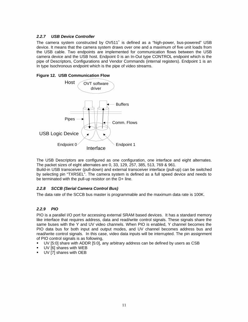
2.2.7 USB Device Controller The camera system constructed by OV511+ is defined as a “high-power, bus-powered” USB device. It means that the camera system draws over one and a maximum of five unit loads from the USB cable. Two endpoints are implemented for communication flows between the USB camera device and the USB host. Endpoint 0 is an In-Out type CONTROL endpoint which is the pipe of Descriptors, Configurations and Vendor Commands (internal registers). Endpoint 1 is an In type Isochronous endpoint which is the pipe of video streams. Figure 12. USB Communication Flow
The USB Descriptors are configured as one configuration, one interface and eight alternates. The packet sizes of eight alternates are 0, 33, 129, 257, 385, 513, 769 & 961. Build-in USB transceiver (pull-down) and external transceiver interface (pull-up) can be switched by selecting pin “TXRSEL”. The camera system is defined as a full speed device and needs to be terminated with the pull-up resistor on the D+ line.
2.2.8 SCCB (Serial Camera Control Bus) The data rate of the SCCB bus master is programmable and the maximum data rate is 100K.
2.2.9 PIO PIO is a parallel I/O port for accessing external SRAM based devices. It has a standard memory like interface that requires address, data and read/write control signals. These signals share the same buses with the Y and UV video channels. When PIO is enabled, Y channel becomes the PIO data bus for both input and output modes, and UV channel becomes address bus and read/write control signals. In this case, video data inputs will be interrupted. The pin assignment of PIO control signals is as following, § UV [5:0] share with ADDR [5:0], any arbitrary address can be defined by users as CSB § UV [6] shares with WEB § UV [7] shares with OEB
OVT softwaredriver
Host
Buffers
Comm. Flows
Interface
Pipes
USB Logic Device
Endpoint 0 Endpoint 1

12
Figure 13. PIO Read Cycle Timing Waveforms
Figure 14. PIO Write Cycle Timing Waveforms
OEB/UV[7]
WEB/UV[6]
ADDR[5:0]/UV[5:0]
DATA[7:0]/Y[7:0]
ADDnADD0
DATA0 DATAn
tRC
tCSA tCSX tAA
tAx
tOEZ tOE
OEB/UV[7]
WEB/UV[6]
ADDR[5:0]/UV[5:0]
DATA[7:0]/Y[7:0]
ADD0 ADDn
DATAnDATA0
tWC
tDH
tDS
tWE
tAS tAH

13
Table 4. Parameters of PIO Timing Symbol Parameter Min Max Unit
TOE Output enable access time 15 ns TOEZ Output enable to z delay 15 ns TRC Register read cycle time 100 ns TCSA Chip select access time 30 ns TCSX Chip select to data invalid time 15 ns TAA Address access time 30 ns TAX Address data invalid time 15 ns TWC Register write cycle time 100 ns TWE Write enable pulse width 50 ns TAS Write cycle address set up time 0 ns TAH Write cycle address hold time 0 ns TDS Write cycle data set up time 20 ns TDH Write cycle data hold time 0 ns
2.2.10 Custom ID Custom ID is a specific 8-bit input port that can be pulled up/down to identify company names of manufacturers. The Custom ID is checked by the software driver and may be requested directly from OVT. If no Custom ID is applied, pull-down resistors are also required to avoid bus floating. Pin “IDESL [1:0]” have to be set as “01”.

14
3
3 Pin Definition
3.1 Pin Assignments
Figure 15. 100-Pin PQFP Package
1
VDD
2
VSS
3
Y5
4
Y4
5
Y3
6
Y2
7
Y1
8
Y0
9
IDSEL1
10
IDSEL0
11
SNAPB
12
ENOSC27
13
CUSTOMID7
14
VDD
15
VSS
16
CUSTOMID6
17
CUSTOMID5
18
CUSTOMID4
19
CUSTOMID3
20
CUSTOMID2
21
CUSTOMID1
22
CUSTOMID0
23
CLK27M1
24
CLK27M2
25
RESETB
26
DMNS
27
OSCEN
28
TXRSEL
29
CLK48M1
30
CLK48M2
31 TXDMNS
32 TXDPLS
33 DM
34 DP
35 XVERDATA
36 TXENL
37 DPLS
38 CASB
39 VDD
40 VSS
41 OEB
42 ADDR8
43 ADDR7
44 ADDR6
45 VDD
46 VSS
47 ADDR5
48 ADDR4
49 ADDR3
50 ADDR2
80
79
78
77
76
75
74
73
72
71
70
69
51
52
53
54
55
56
57
58
59
60
61
62
63
64
65
66
67
68
UV7
LEDCTL
PWCK
SPWDN
VSS
VDD
DATA8
DATA9
DATA10
DATA11
DATA12
DATA13
RASB
WEB
VDD
VSS
DATA7
DATA6
DATA5
DATA4
DATA3
DATA2
DATA1
DATA0
VDD
VSS
DATA15
DATA14
ADDR1
ADDR0
100
99
98
97
96
95
94
93
92
91
90
89
88
87
86
85
84
83
82
81
Y6
Y7
PWDN
RESET
SIO0
FODD
SIO1
HREF
VSYNC
VSS
VDD
PCLK
CCLK
UV0
UV1
UV2
UV3
UV4
UV5
UV6
OV 511+

15
3.2 Pin Descriptions
Table 5. Pin Descriptions Items/Pin # Name I/O Function mA Camera Interface 99, 100, 3~8 Y[7:0] IT/OT Camera Y data input 8
PIO data input/output
80~87 UV[7:0] IT/OT Camera UV data input 8
PIO address, read/write control output
89 PCLK IT Camera pixel clock input
93 HREF IT Camera horizontal window reference input
92 VSYNC IT Camera vertical sync. Input
95 FODD IT Camera even/odd field flag input
88 CCLK O Camera clock output. Software programmable 8
97 RESET O Camera hardware reset output 4
98 PWDN O Camera power switch control output 4
SCCB Interface
96 SIO-0 IS/OD SCCB serial data. Pull-up resistor (4.7K Ohm) is required 4
Bi-directional
94 SIO-1 OD SCCB serial clock output. Pull-up resistor (4.7K Ohm) is required
4
DRAM Interface
67~74, 57~64 DATA[15:0] IT/OT DRAM 16-bit data 8
41 OEB O DRAM OE_ output 8
54 WEB O DRAM WE_ output 8
42~44, 47~52 ADDR[8:0] O DRAM address output 8
38 CASB O DRAM CAS_ output 8
53 RASB O DRAM RAS_ output 8
USB Interface
35 XVER_DATA IT USB differential receiver data input (external transceiver)
26 DMNS IT D- input (external transceiver)
37 DPLS IT D+ input (external transceiver)
36 TXENL O Output enable for differential driver (external transceiver) 4
31 TXDMNS O NRZI formatted D- output (external transceiver) 4
32 TXDPLS O NRZI formatted D+ output (external transceiver) 4
33 DM UI/O D- input/output (internal transceiver)
34 DP UI/O D+ input/output (internal transceiver)
Clock & Misc.
25 RESETB IS Power-On Reset input. Low-active
29 CLK_48M1 OSCI 48MHz oscillator/crystal input
30 CLK_48M2 OSCO 48MHz crystal output
23 CLK_27M1 OSCI 27MHz oscillator/crystal input
24 CLK_27M2 OSCO 27MHz crystal output
27 OSC_EN O Power control for oscillator. 1 for power enabled 4
28 TXRSEL IS Internal/external transceiver control. 0 for internal
11 SNAPB IS Snapshot button input. Cleared by the software driver
9~10 IDSEL[1:0] IS VID & PID select. 01 is required
77 SPWDN IS Power down mode select. 1 is required
13, 16~22 CUSTOM_ID[7:0] IS Custom ID inputs

16
Pin Descriptions (continued) Items/Pin # Name I/O Function mA 12 EN_OSC27 IS 27MHz clock input select. 1 for enabled
78 PWCK O Switching power clock output 8
79 LEDCTL O LED control 4
Power & Ground
1, 14, 39, 45, 55, 65 VDD I Power
75, 90
2, 15, 40, 46, 56, 66 VSS I Ground
76, 91
I : Input IS : CMOS Schmitt Trigger Level Input IT : TTL Level Input O : Normal Output OSCI : Oscillator Input OD : Open Drain Output OT : Tri-state Buffer Output OSCO : Oscillator Output UI/O : USB Transceiver Input / Output

17
4
4 Electrical Characteristics Table 6. DC Electrical Characteristics VDD = 5V + 5%, TA = 0 to 70oC Symbol Parameter Condition Min Max Unit
VIH High level input voltage 3.5 (CMOS) ~ 2.0 (TTL)
V
VIL Low level input voltage 1.5 (CMOS) ~ 0.8 (TTL)
V
VT+ Schmitt trigger, positive-going threshold 4.0 (CMOS) V
VT- Schmitt trigger, negative-going threshold 1.0 (CMOS) V
IIH High level input current VIN = VDD -10 10 uA
IIL Low level input current VIN = VSS -10 10 uA
VOH High level output voltage 2.4 V
VOL Low level output voltage 0.4 V
IOZ Tri-state output leakage current VOUT = VSS or VDD -10 10 uA
IDD Quiescent supply current VIN = VSS or VDD 100 uA
CIN Input capacitance 4 pF
COUT Output capacitance 4 pF
Table 7. Absolute Maximum Ratings
Symbol Parameter Rating Unit VDD DC supply voltage -0.3 to 7 V VIN DC input voltage -0.3 to VDD + 0.3 V IIN DC input current + 10 mA TSTG Storage temperature -40 to 125 oC
Table 8. Recommended Operating Conditions
Symbol Parameter Rating Unit VDD DC supply voltage 5V 4.75 to 5.25 V TA Commercial temperature 0 to 70 oC
Table 9. USB DC Electrical Characteristics
Symbol Parameter Condition Min Max Unit ICCS Suspended device 10 uA ILO Hi-Z state data line leakage 0V<Vin<3.3V -10 10 uA VDI Differential input sensitivity | (D+) – (D-) | 0.2 V VCM Differential common mode range 0.8 2.5 V VSE Single ended receiver threshold 0.8 2.0 V VOL Static output low RL 1.5kΩ to 3.6V 0.2 V VOH Static output high RL 1.5kΩ to GND 2.8 3.6 V CIN Transceiver capacitance Pin to GND 20 pF
Table 10. USB Full Speed Output Driver Electrical Characteristics
Symbol Parameter Condition Min Max Unit TR Rise time CL=50pF 4 20 ns Tf Fall time CL=50pF 4 20 ns Trim Rise / Fall time matching (Tr/Tf) 90 110 % VCrs Output signal crossover Voltage 1.3 2.0 V Zdrv Driver output resistance Steady state drive 28 43 Ω

18
5
5 Register Table (Vendor Commands)
5.1 CAMERA INTERFACE
Table 11. Camera Interface Register List Register Address
Register Name
R/W Function Default Value
10h DLYM[1:0] RW Bit 1~0 : Delay modes of video input signals 00 : no delay 01 : delays YUV by one PCLK 10 : delays HREF by one PCLK 11 : delays YUV and HREF by one PCLK
00h
11h PEM[0] RW Bit 0 : Edge modes of PCLK 0 : PCLK negative edge latches video data 1 : PCLK positive edge latches video data
01h
12h PXCNT[6:0] RW Bit 6~0 : Clamped pixel number It defines the clamped pixel number of a horizontal line in increment of 8 pixels. If the pixel number from camera is larger than this number, the spare pixels will be dropped. Clamped Pixel No. = (PXCNT + 1) * 8
27h
13h LNCNT[6:0] RW Bit 6~0 : Clamped line number It defines the clamped line number in increment of 8 lines. If the line number from camera is larger than this number, the spare lines will be dropped. Clamped Line No. = (LNCNT + 1) * 8
1Dh
14h PXDV[1:0] RW Bit 1~0 : Pixel divisor It defines down sampling frequency in the horizontal pixel direction. 00 : divided by 1 01 : divided by 2 10 : divided by 4 11 : divided by 8
01h
15h LNDV[1:0] RW Bit 1~0 : Line divisor It defines down sampling frequency in the vertical line direction. Uses these register bits along with register bit LSTR to retain even or odd lines. 00 : divided by 1 01 : divided by 2 10 : divided by 4 11 : divided by 8
01h
16h M400[0] RW Bit 0 : 8 bit (Y channel only) / 16 bit (Y & UV channels) data input select 0 : 8 bit data in Y channel (UV channel is ignored) 1 : 16 bit data in both Y & UV channels. Uses this register bit along with register bit M420 to select 422/420 formats.
01h
17h LSTR[0] RW Bit 0 : Reserved lines for downing sampling 0 : even lines (2, 4, 6, 8, ……) 1 : odd lines (1, 3, 5, 7, ……)
00h
18h M420[1] YFIR[0]
RW Bit 1 : YUV422/420 0 : YUV 4:2:2 1 : YUV 4:2:0 Bit 0 : Y channel low pass filter 0 : disabled 1 : enabled
00h
•• Snapshot Operation – a full set of camera interface registers are duplicated for hardware snapshot operation. These registers replace the normal ones for taking snapshot frame so that the snapshot frame can be different settings from normal frame. The followings are the snapshot registers.

19
Camera Interface Register List (continued) Register Address
Register Name
R/W Function Default Value
19h SPDLY[7:0] RW Bit 7~0 : Captured frame for snapshot It defines which frame (one frame only) after snapshot function is triggered will be captured. 00000000 : the first frame 10000001 ~ 11111111 : the 2nd ~ 128th frame
00h
1Ah SNPX[6:0] RW Bit 6~0 : Clamped pixel number for snapshot 4Fh 1Bh SNLN[6:0] RW Bit 6~0 : Clamped line number for snapshot 1Dh 1Ch SNPD[1:0] RW Bit 1~0 : Pixel divisor for snapshot 00h 1Dh SNLD[1:0] RW Bit 1~0 : Line divisor for snapshot 01h 1Eh SN400[0] RW Bit 0 : 8/16 bit data input for snapshot 01h 1Fh SNALSTR[2]
SN420[1] SNYFIR[0]
RW Bit 2 : Reserved lines for down sampling for snapshot Bit 1 : YUV422/420 for snapshot Bit 0 : Y channel low pass filter for snapshot
04h
5.2 DRAM INTERFACE
Table 12. DRAM Interface Register List Register Address
Register Name
R/W Function Default Value
20h ENFC[0] RW Bit 0 : Image flow control 0 : disabled, doesn’t guarantee a complete image frame 1 : enabled, guarantees a complete image frame
01h
21h ARCP[0] RW Bit 0 : Auto read cycle predictor It predicts the number of read cycles that will be inserted besides write cycles. 0 : disabled, use register bit MRC for manual setting 1 : enabled
01h
22h MRC[3:0] RW Bit 3~0 : Manual read cycle insertion It defines the number of read cycles that will be inserted besides write cycles. Read cycles = MRC + 1
01h
23h RFC[5:0] RW Bit 5~0 : Refresh counter 1Ah
5.3 ISO FIFO
Table 13. ISO FIFO Register List Register Address
Register Name
R/W Function Default Value
30h PKSZ[4:0] RW Bit 4~0 : Packet size It defines the packet size of ISO FIFO which is available from 00000 (0 bytes) to 11110 (960 bytes). The packet size must match with the current alternate setting. Packet size = (32 * PKSZ) bytes
08h
31h NZPK[3] ENPKNO[1]
ENCE[0]
RW Bit 3 : Zero packet inserted after EOF (image end of frame flag) 0 : disabled 1 : enabled Bit 1 : Packet No. insertion It inserts one extra byte at the end of each packet as the packet number. It counts in sequence, but only the packet containing SOF (image start of frame flag) uses “00”. 0 : disabled 1 : enabled Bit 0 : Compressed data non-zero (01) insertion It inserts “01” at the 7th byte of the packet if the 1st ~8th incoming compressed data are all “00”. 0 : enabled 1 : disabled
03h

20
5.4 PIO
Table 14. PIO Register List Register Address
Register Name
R/W Function Default Value
38h ENPIO[7] PIORW[6] PADD[5:0]
W Bit 7 : Parallel IO operation 0 : disabled 1 : enabled. UV channel changes to output mode for parallel IO operation. Register bits PADD[5:0] output to pin UV[5:0]. UV[6] performs as OEB, while UV[7] performs as WEB. Y channel is bi-directional. The direction depends on read/write operation of PIO. The bus cycle is executed once only after USB host write to this register and ENPIO = 1. Write data has to be placed in register bits PDATA[7:0] before launching the PIO write cycle. Read data is returned in register bits PDATA[7:0] after launching the PIO read cycle. Bit 6 : Read/write cycle for PIO operation 0 : read cycle 1 : write cycle Bit 5~0 : address port of PIO operation
00h
39h PDATA[7:0] RW Bit 7~0 : data port of PIO operation 00h 3Eh ENTP[3]
TPS[2:0] W Bit 3 : BIST operation for OV511+
0 : disabled 1 : enabled Bit 2~0 : BIST functions select
00h
•• PIO R/W sequence examples Write cycles
1. Writes to data port (PDATA, register 39h) 2. Enables PIO (ENPIO, register 38h), sets up address (PADD, register 38h), & selects
write cycle (PIORW, register 38h) 3. Disables PIO (ENPIO, register 38h)
Read cycles 1. Enables PIO (ENPIO, register 38h), sets up address (PADD, register 38h), & selects
read cycle (PIORW, register 38h) 2. Reads from data port (PDATA, register 39h)
5.5 SCCB
Table 15. SCCB Register List Register Address
Register Name
R/W Function Default Value
40h TMOUT[2] NOACK[1]
IDLE[0]
R Bit 2 : Time out flag for SCCB operation. Sets when timer reaches the value set by register bits TMO[4:0]. Bit 1 : No acknowledge on SCCB bus. It’s valid when register bit IDLE is set. Bit 0 : SCCB bus idle flag
00h
40h ENABORT[4] TYPE[2:1]
STARTSCCB[0]
W Bit 4 : Aborts SCCB bus cycle if SCCB slave doesn’t response (no acknowledge) Bit 2~1 : Types of SCCB read/write sequence 00 : 3 byte write cycle, in sequence of slave ID (SID), sub address (SWA) & SCCB data (SIO-0) 01 : 2 byte write cycle, in sequence of slave ID (SID) & sub address (SMA) 1x : 2 byte read cycle, in sequence of slave ID (SRA) & SCCB data (SIO-0) Bit 0 : Launches a new SCCB bus cycle if set SCCB won’t launch a new cycle if it doesn’t finish the previous bus cycle.
00h

21
SCCB Register List (continued) Register Address
Register Name
R/W Function Default Value
41h SID[7:0] RW Bit 7~0 : SCCB slave ID for 3 or 2 byte write cycles 00h 42h SWA[7:0] RW Bit 7~0 : Sub address for 3 byte write cycles 00h 43h SMA[7:0] RW Bit 7~0 : Sub address for 2 byte write cycles 00h 44h SRA[7:0] RW Bit 7~0 : Slave ID for 2 byte read cycles 00h 45h SIO-0[7:0] RW Bit 7~0 : SCCB read/write data port 00h 46h PSC[7:0] RW Bit 7~0 : SCCB clock prescaler
It defines prescaler values for SCCB clock. SCCB bit rate = 93.5 KHz / ( PSC + 1)
00h
47h TMO[4:0] RW Bit 4~0 : Time out counter A timer starts to count SCCB clocks when SCCB bus cycle is launched. When the timer reaches TMO, TMOUT is set.
00h
•• Snapshot Operation - During the period of hardware snapshot operation, OV511+ first
launches a 3 byte SCCB write cycle to SCCB slave device, such as camera, by using register 48h and 49h. It permits SCCB slave device to modify the internal settings before taking the snapshot.
SCCB Register List (continued) Register Address
Register Name
R/W Function Default Value
48h SPA[7:0] W Bit 7~0 : Sub address of the SCCB write cycle for snapshot operation
00h
49h SPD[7:0] W Bit 7~0 : Data port of the SCCB write cycle for snapshot operation 00h
•• SCCB R / W Sequence Examples Setup stage
1. Writes to slave ID (SID, register 41h) 3 byte write cycles
1. Writes to sub address (SWA, register 42h) 2. Writes to data port (SIO-0, register 45h) 3. Writes to control bits to select write cycle and launch SCCB cycles (TYPE,
STARTSCCB, register 40h) 2 byte dummy write cycles (In order to set sub address of SCCB slave device for the next coming read cycle)
1. Writes to sub address (SMA, register 43h) 2. Writes to control bits to select write cycle and launch SCCB cycles (TYPE,
STARTSCCB, register 40h) 2 byte read cycles
1. Writes to sub address (SRA, register 44h) 2. Writes to control bits to select read cycle and launch SCCB cycles (TYPE,
STARTSCCB, register 40h) 3. Reads from status bits (TMOUT, NOACK, IDLE, register 40h) 4. Reads from data port (SIO-0, register 45h)

22
5.6 SYSTEM CONTROL
Table 16. System Control Register List Register Address
Register Name
R/W Function Default Value
50h RST[6:0] RW Bit 0 : Software reset for Flush Bit 1 : Software reset for SCCB Bit 2 : Software reset for ISO FIFO Bit 3 : Software reset for OmniCE Bit 4 : Software reset for DRAM interface Bit 5 : Software reset for camera interface Bit 6 : Software reset for OV511+ & registers
00h
51h CLKDIV[4:0] RW Bit 4~0 : Camera clock divisor It defines the frequency of camera clock output CCLK. CCLK is divided down based on external clock inputs CLK_48 or CLK_27. The maximum frequency of CLK_27 that OV511+ can handle is 27MHz. If both CLK_27 and CLK_48 clock inputs are enabled by pulling up pin “EN_OSC27”, CLK_27 is chosen in support of camera clock. 00000 : no division (CLK_27) 11111 : CLK_27 divided by 32 If only CLK_48 clock input is enabled by pulling down pin “EN_OSC27”, CLK_48 is divided by 2 and provides camera clock.
00h
52h SNAP[3:0] RW Bit 0 : Hardware snapshot 0 : disabled 1 : enabled Bit 1 : Releases hardware snapshot bottom in sequence of 0,1,0 Bit 2 : Software snapshot 0 : disabled 1 : enabled Bit 3 : Snapshot status (read only)
01h
53h EN_SYS[0] W Bit 0 : Software system initialization Before system is initialized, system clocks will be stopped to meet the requirement of power consumption for the whole system to be less than 100mA. After that, it can increase to max. 500mA for USB bus powered device. If pin “EN_SYSTEM” is pulled down, this bit controls system initialization. Otherwise, system is initialized right after power-on reset. 0 : system is not initialized 1 : system is initialized
00h
54h PWCK[1:0] RW Bit 1~0 : Switching power clock output select 00 : 24KHz 01 : 48KHz 10 : 96KHz 11 : 192KHz
02h
55h LEDCTL RW Bit 0 : LED control 00h 5Eh USR[7:0] RW Bit 7~0 : User defined read/write register bits 00h 5Fh CID[7:0] R Bit 7~0 : Custom ID which links to input pins “CUSTOM_ID”
It is checked by the software driver to identify company names. It may be requested directly from OVT. The registered custom ID can be coded by pulling up or down resistors through pins “CUSTOM ID”. If no custom ID is applied, pull-up/down resistors are also requested to avoid floating.
~

23
5.7 OmniCE
Table 17. OmniCE Register List Register Address
Register Name
R/W Function Default Value
70h PRH_Y[5:0] RW Bit 5~0 : Predication range in horizontal direction for Y channel One horizontal line is divided into horizontal segments for prediction. It defines the number of pixels contained in one horizontal segment of Y channel. Pixels in the segment except the first one are predicted by the first pixel of this segment.
1Fh
71h PRH_UV[5:0] RW Bit 5~0 : Prediction range in horizontal direction for UV channel 05h 72h PRV_Y[7:0] RW Bit 7~0 : Predication range in vertical direction for Y channel
One image frame is divided into vertical segments for prediction. It defines the number of pixels contained in one vertical segment of Y channel. Pixels in the segment except the first one are predicted by the first pixel of this segment.
06h
73h PRV_UV[7:0] RW Bit 7~0 : Predication range in vertical direction for UV channel 06h 74h QTH_Y[7:0] RW Bit 7~0 : Quantization threshold in horizontal direction for Y
channel 14h
75h QTH_UV[7:0] RW Bit 7~0 : Quantization threshold in horizontal direction for UV channel
03h
76h QTV_Y[7:0] RW Bit 7~0 : Quantization threshold in vertical direction for Y channel
04h
77h QTV_UV[7:0] RW Bit 7~0 : Quantization threshold in vertical direction for UV channel
04h
78h UV_en[2] Y_en[1]
CE_en[0]
RW Bit 0 : OmniCE 0 : disabled 1: enabled Bit 1 : Y channel operation 0 : disabled 1 : enabled Bit 2 : UV channel operation 0 : disabled 1 : enabled
06h
79h LTEN_UV[1] LTEN_Y[0]
RW Bit 0 :Look-up table for Y channel 0 : disabled 1 : enabled Bit 1 : Look-up table for UV channel 0 : disabled 1 : enabled
00h
80~9Fh LT_Y RW Bit 7~0 : Programmable look-up table for Y channel ~ A0~BFh LT_UV RW Bit 7~0 : Programmable look-up table for UV channel ~
24
6
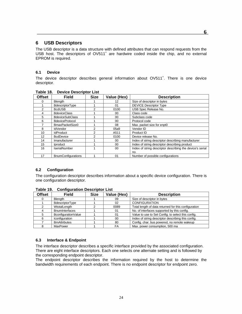
6 USB Descriptors The USB descriptor is a data structure with defined attributes that can respond requests from the USB host. The descriptors of OV511+ are hardwire coded inside the chip, and no external EPROM is required.
6.1 Device The device descriptor describes general information about OV511+. There is one device descriptor. Table 18. Device Descriptor List Offset Field Size Value (Hex) Description
0 Blength 1 12 Size of descriptor in bytes 1 BdescriptorType 1 01 DEVICE Descriptor Type 2 BcdUSB 2 0100 USB Spec Release No. 4 BdeviceClass 1 00 Class code 5 BdeviceSubClass 1 00 Subclass code 6 BdeviceProtocol 1 00 Protocol code 7 BmaxPacketSize0 1 08 Max. packet size for enpt0 8 IdVendor 2 05a9 Vendor ID 10 IdProduct 2 A511 Product ID 12 BcdDevice 2 0100 Device release No. 14 Imanufacturer 1 00 Index of string descriptor describing manufacturer 15 Iproduct 1 00 Index of string descriptor describing product 16 IserialNumber 1 00 Index of string descriptor describing the device's serial
no. 17 BnumConfigurations 1 01 Number of possible configurations
6.2 Configuration The configuration descriptor describes information about a specific device configuration. There is one configuration descriptor. Table 19. Configuration Descriptor List Offset Field Size Value (Hex) Description
0 Blength 1 09 Size of descriptor in bytes 1 BdescriptorType 1 02 CONFIGURATION 2 WtotalLength 2 0089 Total length of data returned for this configuration 4 BnumInterfaces 1 01 No. of interfaces supported by this config. 5 BconfigurationValue 1 01 Value to use to Set Config. to select this config. 6 Iconfiguration 1 00 Index of string descriptor describing this config. 7 BmAttributes 1 80 Config. char. bus powered, no remote wakeup 8 MaxPower 1 FA Max. power consumption, 500 ma
6.3 Interface & Endpoint The interface descriptor describes a specific interface provided by the associated configuration. There are eight interface descriptors. Each one selects one alternate setting and is followed by the corresponding endpoint descriptor. The endpoint descriptor describes the information required by the host to determine the bandwidth requirements of each endpoint. There is no endpoint descriptor for endpoint zero.

25
6.3.1 Alternate 0 Table 20. Interface Descriptor List of Alternate 0 Offset Field Size Value (Hex) Description
0 Blength 1 09 Size of descriptor in bytes 1 BdescriptorType 1 04 INTERFACE 2 BinterfaceNumber 1 00 No. of interface 3 BalternateSetting 1 00 Value used to select alternate setting 4 BnumEndpoints 1 01 No. of endpoints used by this interface 5 BinterfaceClass 1 FF Class code 6 BinterfaceSubClass 1 00 SubClass code 7 BinterfaceProtocol 1 00 Protocol code 8 Iinterface 1 00 Index of string descriptor describing this interface
Table 21. Endpoint Descriptor List of Alternate 0, Packet Size 0 Offset Field Size Value (Hex) Description
0 Blength 1 07 Size of descriptor in bytes 1 BdescriptorType 1 05 ENDPOINT 2 BendpointAddress 1 81 Bit7 1 In Enpt, Bit 6..4 000, Bit 3..0 0001 Enpt No. 3 BmAttributes 1 01 Bit1..0 01 Iso 4 WmaxPacketSize 2 0000 Max. packet size 0 6 Binterval 1 01 Interval for polling enpt for data transfer
6.3.2 Alternate 1
Table 22. Interface Descriptor List of Alternate 1 Offset Field Size Value (Hex) Description
0 Blength 1 09 Size of descriptor in bytes 1 BdescriptorType 1 04 INTERFACE 2 BinterfaceNumber 1 00 No. of interface 3 BalternateSetting 1 01 Value used to select alternate setting 4 BnumEndpoints 1 01 No. of endpoints used by this interface 5 BinterfaceClass 1 FF Class code 6 BinterfaceSubClass 1 00 SubClass code 7 BinterfaceProtocol 1 00 Protocol code 8 Iinterface 1 00 Index of string descriptor describing this interface
Table 23. Endpoint Descriptor List of Alternate 1, Packet Size 33 Offset Field Size Value (Hex) Description
0 Blength 1 07 Size of descriptor in bytes 1 BdescriptorType 1 05 ENDPOINT 2 BendpointAddress 1 81 Bit7 1 In Enpt, Bit 6..4 000, Bit 3..0 0001 Enpt No. 3 BmAttributes 1 01 Bit1..0 01 Iso 4 WmaxPacketSize 2 0021 Max. packet size 33 6 Binterval 1 01 Interval for polling enpt for data transfer
6.3.3 Alternate 2
Table 24. Interface Descriptor List of Alternate 2 Offset Field Size Value (Hex) Description
0 Blength 1 09 Size of descriptor in bytes 1 BdescriptorType 1 04 INTERFACE 2 BinterfaceNumber 1 00 No. of interface 3 BalternateSetting 1 02 Value used to select alternate setting 4 BnumEndpoints 1 01 No. of endpoints used by this interface 5 BinterfaceClass 1 FF Class code

26
Interface Descriptor List of Alternate 2 (continued) 6 BinterfaceSubClass 1 00 SubClass code 7 BinterfaceProtocol 1 00 Protocol code 8 Iinterface 1 00 Index of string descriptor describing this interface
Table 25. Endpoint Descriptor List of Alternate 2, Packet Size 129 Offset Field Size Value (Hex) Description
0 Blength 1 07 Size of descriptor in bytes 1 BdescriptorType 1 05 ENDPOINT 2 BendpointAddress 1 81 Bit7 1 In Enpt, Bit 6..4 000, Bit 3..0 0001 Enpt No. 3 BmAttributes 1 01 Bit1..0 01 Iso 4 WmaxPacketSize 2 0081 Max. packet size 129 6 Binterval 1 01 Interval for polling enpt for data transfer
6.3.4 Alternate 3
Table 26. Interface Descriptor List of Alternate 3 Offset Field Size Value (Hex) Description
0 Blength 1 09 Size of descriptor in bytes 1 BdescriptorType 1 04 INTERFACE 2 BinterfaceNumber 1 00 No. of interface 3 BalternateSetting 1 03 Value used to select alternate setting 4 BnumEndpoints 1 01 No. of endpoints used by this interface 5 BinterfaceClass 1 FF Class code 6 BinterfaceSubClass 1 00 SubClass code 7 BinterfaceProtocol 1 00 Protocol code 8 Iinterface 1 00 Index of string descriptor describing this interface
Table 27. Endpoint Descriptor List of Alternate 3, Packet Size 257 Offset Field Size Value (Hex) Description
0 Blength 1 07 Size of descriptor in bytes 1 BdescriptorType 1 05 ENDPOINT 2 BendpointAddress 1 81 Bit7 1 In Enpt, Bit 6..4 000, Bit 3..0 0001 Enpt No. 3 BmAttributes 1 01 Bit1..0 01 Iso 4 WmaxPacketSize 2 0101 Max. packet size 257 6 Binterval 1 01 Interval for polling enpt for data transfer
6.3.5 Alternate 4
Table 28. Interface Descriptor List of Alternate 4 Offset Field Size Value (Hex) Description
0 Blength 1 09 Size of descriptor in bytes 1 BdescriptorType 1 04 INTERFACE 2 BinterfaceNumber 1 00 No. of interface 3 BalternateSetting 1 04 Value used to select alternate setting 4 BnumEndpoints 1 01 No. of endpoints used by this interface 5 BinterfaceClass 1 FF Class code 6 BinterfaceSubClass 1 00 SubClass code 7 BinterfaceProtocol 1 00 Protocol code 8 Iinterface 1 00 Index of string descriptor describing this interface
Table 29. Endpoint Descriptor List of Alternate 4, Packet Size 385 Offset Field Size Value (Hex) Description
0 Blength 1 07 Size of descriptor in bytes 1 BdescriptorType 1 05 ENDPOINT 2 BendpointAddress 1 81 Bit7 1 In Enpt, Bit 6..4 000, Bit 3..0 0001 Enpt No. 3 BmAttributes 1 01 Bit1..0 01 Iso

27
Endpoint Descriptor List of Alternate 4, Packet Size 385 (continued) 4 WmaxPacketSize 2 0181 Max. packet size 385 6 Binterval 1 01 Interval for polling enpt for data transfer
6.3.6 Alternate 5
Table 30. Interface Descriptor List of Alternate 5 Offset Field Size Value (Hex) Description
0 Blength 1 09 Size of descriptor in bytes 1 BdescriptorType 1 04 INTERFACE 2 BinterfaceNumber 1 00 No. of interface 3 BalternateSetting 1 05 Value used to select alternate setting 4 BnumEndpoints 1 01 No. of endpoints used by this interface 5 BinterfaceClass 1 FF Class code 6 BinterfaceSubClass 1 00 SubClass code 7 BinterfaceProtocol 1 00 Protocol code 8 Iinterface 1 00 Index of string descriptor describing this interface
Table 31. Endpoint Descriptor List of Alternate 5, Packet Size 513 Offset Field Size Value (Hex) Description
0 Blength 1 07 Size of descriptor in bytes 1 BdescriptorType 1 05 ENDPOINT 2 BendpointAddress 1 81 Bit7 1 In Enpt, Bit 6..4 000, Bit 3..0 0001 Enpt No. 3 BmAttributes 1 01 Bit1..0 01 Iso 4 WmaxPacketSize 2 0201 Max. packet size 513 6 Binterval 1 01 Interval for polling enpt for data transfer
6.3.7 Alternate 6
Table 32. Interface Descriptor List of Alternate 6 Offset Field Size Value (Hex) Description
0 Blength 1 09 Size of descriptor in bytes 1 BdescriptorType 1 04 INTERFACE 2 BinterfaceNumber 1 00 No. of interface 3 BalternateSetting 1 06 Value used to select alternate setting 4 BnumEndpoints 1 01 No. of endpoints used by this interface 5 BinterfaceClass 1 FF Class code 6 BinterfaceSubClass 1 00 SubClass code 7 BinterfaceProtocol 1 00 Protocol code 8 Iinterface 1 00 Index of string descriptor describing this interface
Table 33. Endpoint Descriptor List of Alternate 6, Packet Size 769 Offset Field Size Value (Hex) Description
0 Blength 1 07 Size of descriptor in bytes 1 BdescriptorType 1 05 ENDPOINT 2 BendpointAddress 1 81 Bit7 1 In Enpt, Bit 6..4 000, Bit 3..0 0001 Enpt No. 3 BmAttributes 1 01 Bit1..0 01 Iso 4 WmaxPacketSize 2 0301 Max. packet size 769 6 Binterval 1 01 Interval for polling enpt for data transfer
6.3.8 Alternate 7
Table 34. Interface Descriptor List of Alternate 7 Offset Field Size Value (Hex) Description
0 Blength 1 09 Size of descriptor in bytes 1 BdescriptorType 1 04 INTERFACE
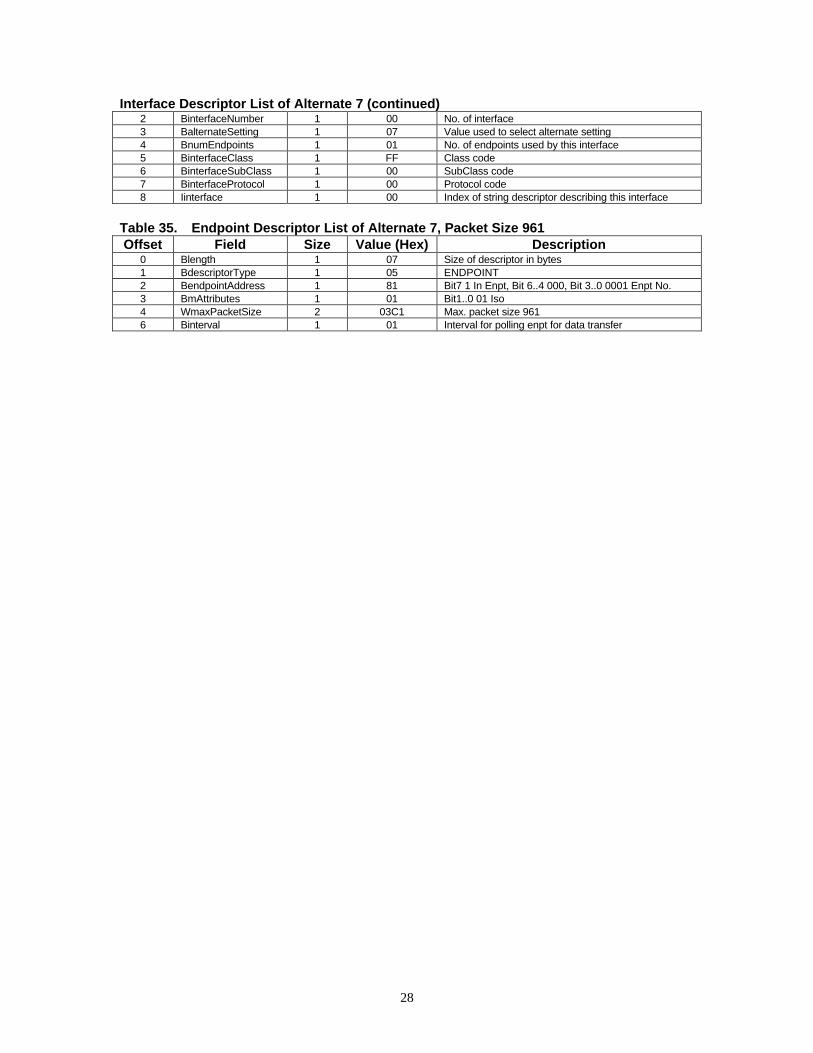
28
Interface Descriptor List of Alternate 7 (continued) 2 BinterfaceNumber 1 00 No. of interface 3 BalternateSetting 1 07 Value used to select alternate setting 4 BnumEndpoints 1 01 No. of endpoints used by this interface 5 BinterfaceClass 1 FF Class code 6 BinterfaceSubClass 1 00 SubClass code 7 BinterfaceProtocol 1 00 Protocol code 8 Iinterface 1 00 Index of string descriptor describing this interface
Table 35. Endpoint Descriptor List of Alternate 7, Packet Size 961 Offset Field Size Value (Hex) Description
0 Blength 1 07 Size of descriptor in bytes 1 BdescriptorType 1 05 ENDPOINT 2 BendpointAddress 1 81 Bit7 1 In Enpt, Bit 6..4 000, Bit 3..0 0001 Enpt No. 3 BmAttributes 1 01 Bit1..0 01 Iso 4 WmaxPacketSize 2 03C1 Max. packet size 961 6 Binterval 1 01 Interval for polling enpt for data transfer
29
7
7 Software Package The followings are software drivers that are or will be supported by OVT. § Stream Class MiniDriver - A WDM (Microsoft Win32 Driver Model) stream class driver
that supports the OVT USB camera system in the Microsoft Windows 98 and Windows 2000. This driver is the bottom level of the software system, and it completes all actual control actions.
§ Video for Windows Compatible Driver - The VFW is the standard interface of Microsoft for Video Capture drivers. Package contains a VFW-to-WDM mapper extension DLL. It adds some pages in Video source property control dialog. This driver allows user control every custom property.
§ TWAIN Source Control Driver - This driver is compatible with Microsoft still image architecture in Windows 98. It allows standard still image oriented application which use the TWAIN API to use the OVT USB Camera system.
§ DirectShow Filter - This software component allows users to control every custom property in DirectShow graph.
§ Installation Software - The installation software is responsible for setting up all camera software components.
30
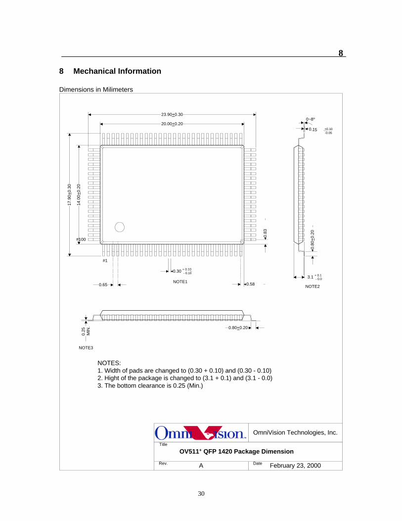
8
8 Mechanical Information Dimensions in Milimeters
OmniVision Technologies, Inc.
Title
OV511+ QFP 1420 Package Dimension
A February 23, 2000Rev. Date
0.80+0.20
3.1
0.80
+0.
20
0~8o
0.15 +0.10-0.05
20.00+0.20
23.90+0.30
14.0
0+0.
20
17.9
0+0.
30
#1
#100
0.65
0.30 + 0.10 - 0.10
0.58
0.83
+ 0.1 - 0.0
0.25
M
IN.
NOTES:1. Width of pads are changed to (0.30 + 0.10) and (0.30 - 0.10)2. Hight of the package is changed to (3.1 + 0.1) and (3.1 - 0.0)3. The bottom clearance is 0.25 (Min.)
NOTE1NOTE2
NOTE3