origin of emission and susceptibility in ics. march 2008 2 emission of em waves susceptibility to em...
TRANSCRIPT
Origin of Emission and Susceptibility in ICs
2 March 2008
Emission of EM wavesSusceptibility to EM waves
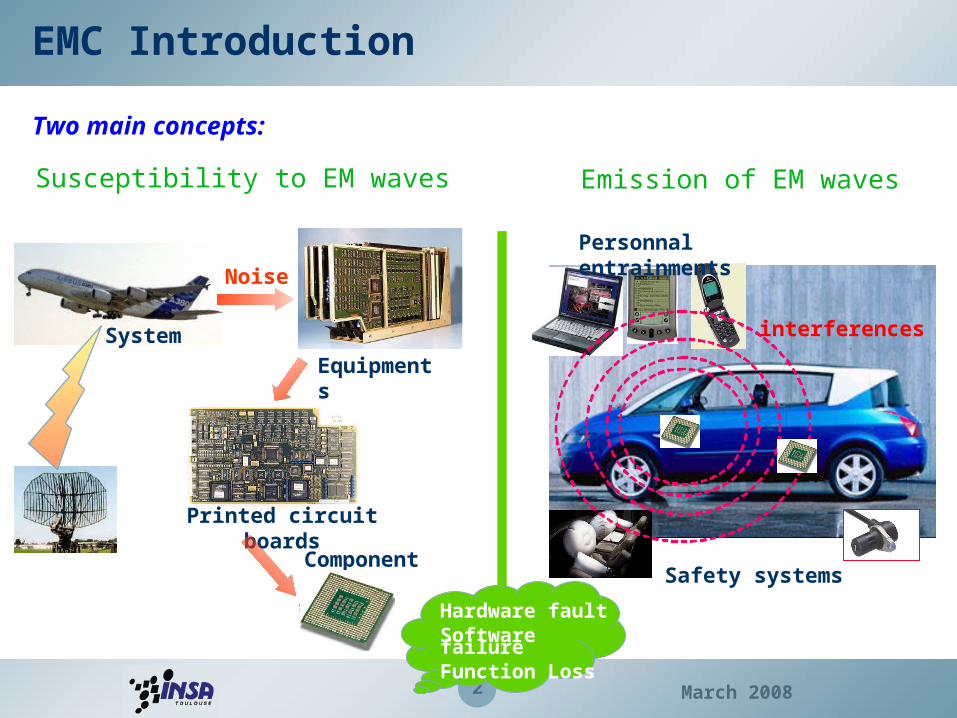
EMC Introduction
Two main concepts:
Personnal entrainments
Safety systems
interferences
Hardware faultSoftware failureFunction Loss
Components
Printed circuit boards
Equipments
System
Noise
3 March 2008
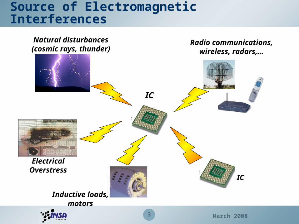
Natural disturbances (cosmic rays, thunder)
Radio communications, wireless, radars,…
Electrical Overstress
Inductive loads, motors
IC
Source of Electromagnetic Interferences
IC

4 March 2008
VDD
VSS
Output capa
Vin
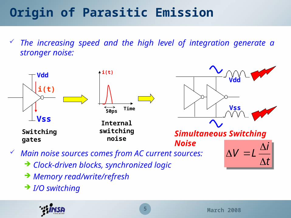
Origin of Parasitic Emission
Basic mechanisms for core current: CMOS inverter exemple
IDD (0.1mA)
ISS (0.1mA)
IDD (0.1mA)
ISS (0.1mA)
VOUT
Switching current
Voltage Time
Time
5 March 2008
Origin of Parasitic Emission
The increasing speed and the high level of integration generate a stronger noise:
Vss
Vdd
50ps
i(t)
Time
Switching gatesInternal
switching noise
Vdd
Vss
i(t)
Main noise sources comes from AC current sources: Clock-driven blocks, synchronized logic Memory read/write/refresh I/O switching
Simultaneous Switching Noise
t
iLV
t
iLV
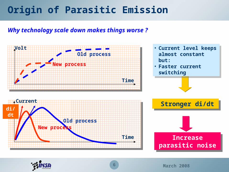
6 March 2008
Stronger di/dt Stronger di/dt
Increase parasitic noise
Increase parasitic noise
Time
New process
VoltOld process
Why technology scale down makes things worse ?
• Current level keeps almost constant but:
• Faster current switching
• Current level keeps almost constant but:
• Faster current switching
Time
Current
di/dt
New processOld process
Origin of Parasitic Emission
7 March 2008
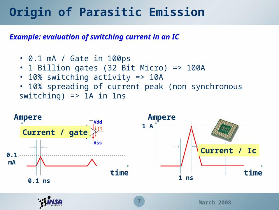
Origin of Parasitic Emission
Example: evaluation of switching current in an IC
• 0.1 mA / Gate in 100ps• 1 Billion gates (32 Bit Micro) => 100A• 10% switching activity => 10A• 10% spreading of current peak (non synchronous switching) => 1A in 1ns
0.1 mA
Ampere
0.1 nstime
Vdd
Vss
i(t)Current / gate
Ampere
1 nstime
Current / Ic
1 A

8 March 2008
Origin of Parasitic Emission
Example: evaluation of SSN
L=0.6nH/mm
L=1nH/mm
Lead = 10 mm
1 A en 1 ns
Evaluate SSN amplitude
VDD
VSS
Lead = 10 mm
mm/nHL 1
t
iLV
Vns
AnHV 20
1
120
Puce
9 March 2008
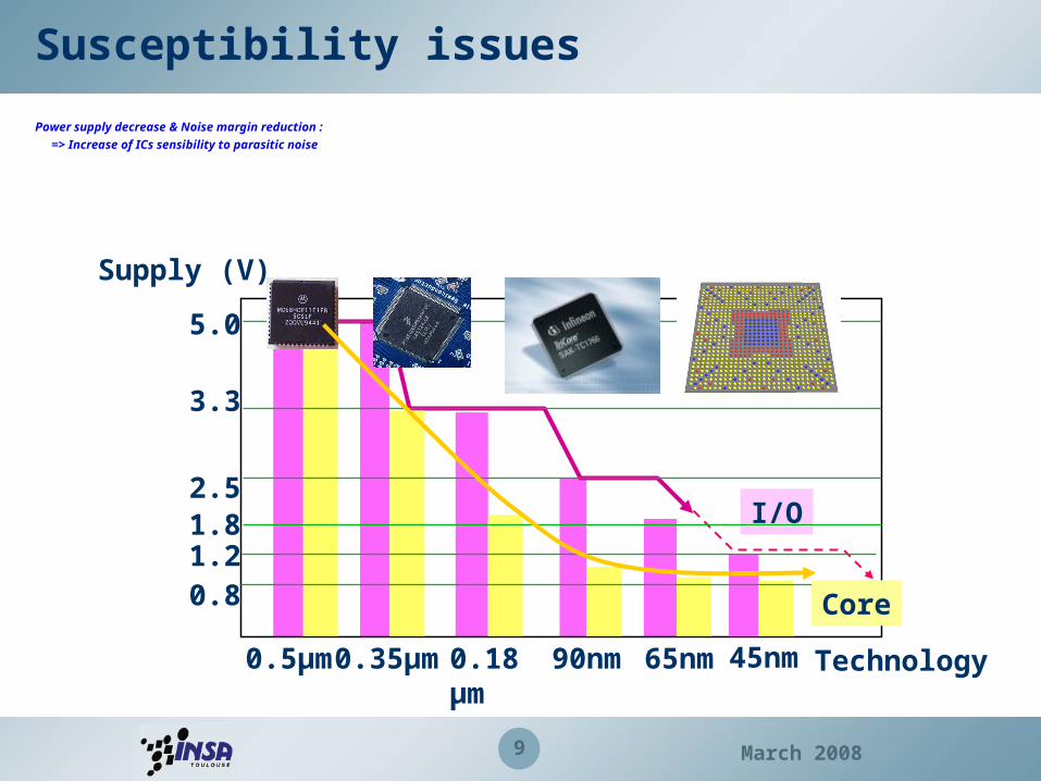
5.0
3.3
2.51.8
0.5µm 0.35µm 0.18µm 90nm 65nm Technology
0.8
Supply (V)
1.2
45nm
I/O
Core
Power supply decrease & Noise margin reduction :
=> Increase of ICs sensibility to parasitic noise
Susceptibility issues
10 March 2008
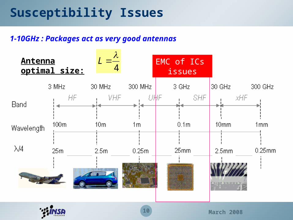
EMC of ICs issues
1-10GHz : Packages act as very good antennas
Susceptibility Issues
Antenna optimal size:4
L
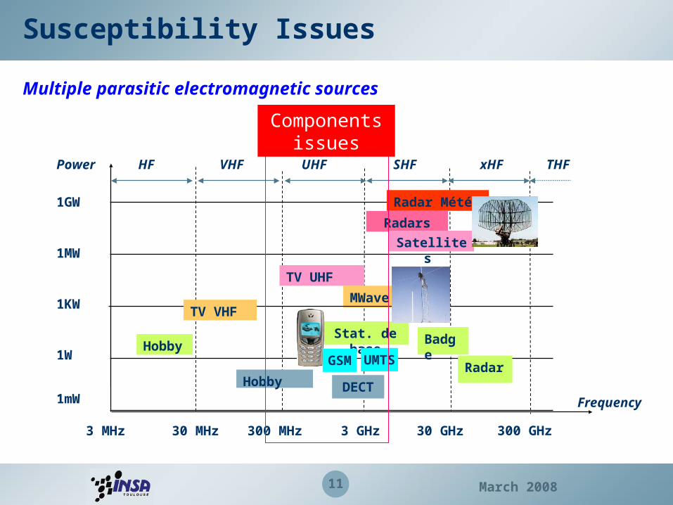
11 March 2008
Hobby
Hobby
TV UHF
Radars
Satellites
MWave
Badge
DECT
Stat. de base
1W
Frequency
1MW
1KW
1GW Radar Météo
3 MHz 30 MHz 300 MHz 3 GHz 30 GHz 300 GHz
Power
1mW
HF VHF UHF SHF xHF THF
Radar UMTS
TV VHF
Multiple parasitic electromagnetic sources
GSM
Susceptibility Issues
Components issues

12 March 2008
Barber, Herke, IEE Electromagnetic Hazard, 1994
Immunity increases with Freq
Immunity increases with Freq
Immunity suddenly decreases?
Immunity suddenly decreases?
Susceptibility trends vs frequency
Susceptibility Issues

13 March 2008
Susceptibility Issues
Desynchronization issues
Jitter is becoming increasingly important in design of logic circuit due to rising operating frequencies.
The increase of operating frequencies of digital circuits reduces their dynamic margin
EMI induced jitter
EMI induced jitter
Bit error
Dynamic failure
EMI on supply

14 March 2008
Emission / Susceptibility Issues
Block type Emission SusceptibilityFast digital I/O ++ -
Power switch output ++ --
Oscillator / PLL / Clock circuitry ++ ++
Charge pump ++ --
Digital block supply + -
Analog input -- ++
DC/DC converter + ++
15 March 2008
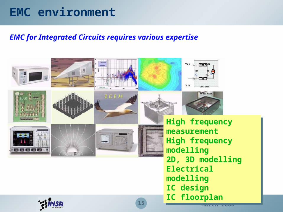
High frequency measurementHigh frequency modelling2D, 3D modellingElectrical modellingIC designIC floorplan
High frequency measurementHigh frequency modelling2D, 3D modellingElectrical modellingIC designIC floorplan
EMC for Integrated Circuits requires various expertise
EMC environment

EMC Measurement methods
17 March 2008
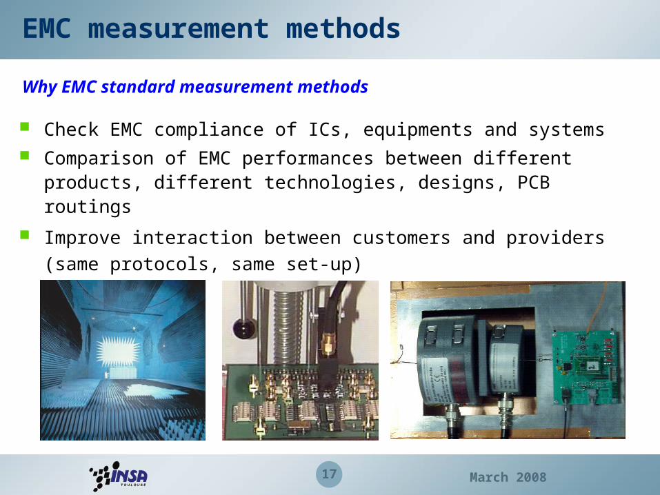
EMC measurement methods
Why EMC standard measurement methods
Check EMC compliance of ICs, equipments and systems Comparison of EMC performances between different products, different
technologies, designs, PCB routings
Improve interaction between customers and providers (same protocols,
same set-up)
18 March 2008
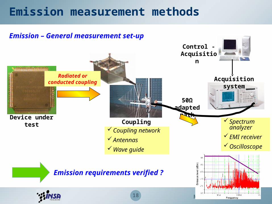
Emission measurement methods
Device under testCoupling device
Coupling network
Antennas
Wave guide
Acquisition system
Spectrum analyzer
EMI receiver
Oscilloscope
Emission – General measurement set-up
Radiated or conducted coupling
50Ω adapted path
Control - Acquisition
Emission requirements verified ?

19 March 2008
IEC 61967-2
(TEM : 1GHz)
IEC 61967-3/6
(Near field scan, 5GHz)
IEC 61967-4
(1/150 ohm, 1 GHz)
IEC 61967-5
(WBFC, 1 GHz)
IEC 61967-7
(Mode Stirred Chamber: 18 GHz)
IEC 61967-2
(GTEM 18 GHz)
International standards for IC emission measurement methods
Emission measurement methods

20 March 2008
Emission measurement methods
Example of emission measurement set-up – TEM cell measurement
Spectrum Analyzer
Pre-amplifierGTEM cell
Shielding
Septum
Far end (to absorbers50 termination)
aperture 1
aperture 2 Near end (to receiver)
Chip under test
Emission spectrum
21 March 2008
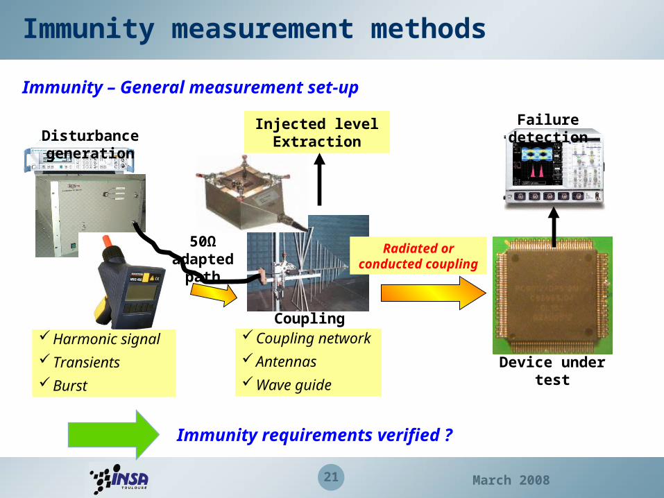
Immunity measurement methods
Immunity – General measurement set-up
Device under test
Coupling deviceCoupling network
Antennas
Wave guide
Radiated or conducted coupling
Disturbance generation
Harmonic signal
Transients
Burst
50Ω adapted path
Failure detectionInjected level Extraction
Immunity requirements verified ?
22 March 2008
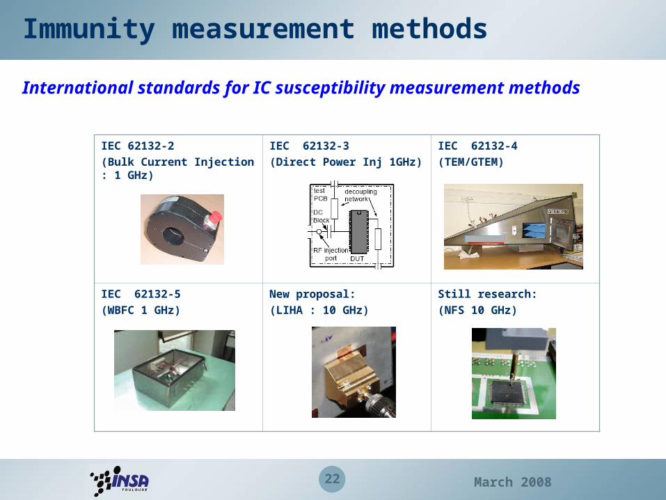
IEC 62132-2
(Bulk Current Injection : 1 GHz)
IEC 62132-3
(Direct Power Inj 1GHz)
IEC 62132-4
(TEM/GTEM)
IEC 62132-5
(WBFC 1 GHz)
New proposal:
(LIHA : 10 GHz)
Still research:
(NFS 10 GHz)
International standards for IC susceptibility measurement methods
Immunity measurement methods
23 March 2008
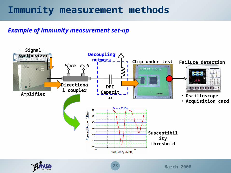
Immunity measurement methods
Example of immunity measurement set-up
DPI Capacitor
Decoupling network Chip under test
Pforw Prefl
Directional coupler
Signal Synthesizer
Amplifier
Failure detection
• Oscilloscope• Acquisition card
Susceptibility threshold
24 March 2008
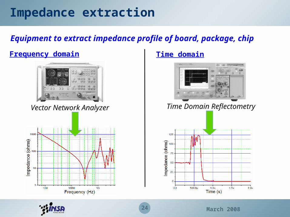
Impedance extraction
Frequency domain Time domain
Vector Network Analyzer Time Domain Reflectometry
Equipment to extract impedance profile of board, package, chip

25 March 2008
EMC equipments
Vector Network Analyzer 10 GHz (100 K€)
Signal Synthesizer 6 GHz (20 K€) GTEM cell 18 GHz
(15 K€)
Spectrum analyzer 40 GHz (40 K€)
Amplifier 3 GHz 100W (60 K€)
Main equipments for EMC – typical prices
Expensive …. Complete EMC laboratory : 500 K€