organization and architecture of the renesas rx63n ...jmconrad/ecgr4101-2013... · organization and...
TRANSCRIPT

Renesas Electronics America Inc.
© 2013 Renesas Electronics America Inc. All rights reserved.
Organization and Architecture of the Renesas RX63N Microcontroller Board Chapter 3
Embedded Systems using the RX63N
00000-A
Rev. 0.1 9/15/2013

© 2013 Renesas Electronics America Inc. All rights reserved. 2
In this chapter we will learn:
Basic organization of computers Architecture of the Renesas RX63N board Endianness, data arrangement, and bus specification
in RX63N CPU Data types, operating modes, and memory map of
RX63N CPU

© 2013 Renesas Electronics America Inc. All rights reserved. 3
Introduction to Computer Organization & Architecture Computer systems looked at from a hierarchical point of
view Four basic functions for a computer to perform are:
1. Data processing 2. Data storage 3. Data movement 4. Data control
The following illustration outlines how data flows between the differend components

Structural Components of a Computer
The four main structural components of a computer are: CPU: Processes the data and controls the operation of
computer. Memory: Stores data. I/O: Moves the data between the computer and the external
environment. System Interconnection: Provides a mechanism for
transferring data or communicating between components such as the CPU, main memory, and I/O.
© 2013 Renesas Electronics America Inc. All rights reserved. 4

Central Processing Unit
The Central Processing Unit (CPU) is the most complex component of the system
The components that make up the CPU are: Control Unit: Controls the operation of the CPU. Arithmetic and Logic Unit (ALU): Performs the computer’s
data processing functions. Registers: Provides internal storage for the CPU. They store
ALU operands. Interconnections: Provides a mechanism for transferring data
or communicating between components such as the Control Unit, ALU, and registers.
© 2011 Renesas Electronics America Inc. All rights reserved. 5

Architecture of the Renesas RX63N
The RX63N microcontroller architecture has the following components: Central Processing Unit:
– CPU: It is a 32-bit RX CPU with maximum operating frequency of 100MHz.
– Floating Point Unit (FPU): This unit is a single precision (32-bit) floating point unit which supports data type
Memory: – ROM: RX63N variants have the following ROM capacities:
ROMless, 256 Kbytes, 384 Kbytes, 512 Kbytes, 768 Kbytes, 1Mbyte, 1.5,Mbytes, 2Mbytes;
– RAM: Its variants have the following capacities: 64 Kbytes, 128 Kbytes, 192 Kbytes, 256 Kbytes.
– E2 Data Flash: Its capacity is 32 Kbytes.
© 2011 Renesas Electronics America Inc. All rights reserved. 6

Architecture of the Renesas RX63N Cont.
Clock Generation Circuit: – The clock generation circuit consists of two circuits; a main
clock oscillator and a sub clock oscillator. – The system clock (ICLK) operates at up to 100 MHz – The peripheral clock (PCLK) and external bus clock (BCLK)
operate at up to 50 MHz Reset:
– There are various reset sources available such as: pin reset, power-on reset, watchdog timer reset, and deep software standby reset.
Voltage detection circuit: – When the voltage available on VCC falls below the voltage
detection level (Vdet), an internal reset or internal interrupt is generated.
© 2011 Renesas Electronics America Inc. All rights reserved. 7

Architecture of the Renesas RX63N Cont.
External bus extension: – The external address space is divided into nine areas: CS0
to CS7 and SDCS – A chip-select signal (CS0# to CS7#, SDCS#) can be output
for each area – Each area is specifiable as an 8-, 16-, or 32-bit bus space
Direct Memory Access (DMA): – The DMA system consists of three different controllers – DMA controller: Has four channels and three transfer
modes; normal transfer, repeat transfer, and block transfer. – EXDMA controller: Has two channels and four transfer
modes; normal transfer, repeat transfer, block transfer, and cluster transfer.
– Data transfer controller: Has three transfer modes; normal transfer, repeat transfer, and block transfer.
© 2011 Renesas Electronics America Inc. All rights reserved. 8

Architecture of the Renesas RX63N Cont.
I/O ports: – The main modules of I/O ports are programmable I/O ports. – The number of programmable I/O ports depends on the
package Timers:
– Seven timers are available the controlling the sequence of events or processes. Some timers are:
– Watchdog timer (14 bits) – 8-bit timers – Compare-match timer (16 bits)
Communication function: – Controllers used for communicating with the outside world,
examples: – Ethernet controller (10 or 100 Mbps) – USB 2.0 host/function module (USB 2.0, up to 12 Mbps) – Serial communication interfaces (13 channels) – I2C bus interfaces (up to 1 Mbps)
© 2011 Renesas Electronics America Inc. All rights reserved. 9
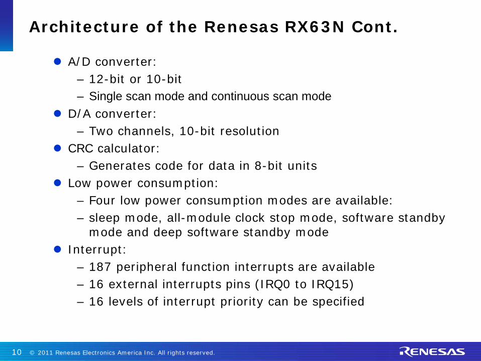
Architecture of the Renesas RX63N Cont.
A/D converter: – 12-bit or 10-bit – Single scan mode and continuous scan mode
D/A converter: – Two channels, 10-bit resolution
CRC calculator: – Generates code for data in 8-bit units
Low power consumption: – Four low power consumption modes are available: – sleep mode, all-module clock stop mode, software standby
mode and deep software standby mode Interrupt:
– 187 peripheral function interrupts are available – 16 external interrupts pins (IRQ0 to IRQ15) – 16 levels of interrupt priority can be specified
© 2011 Renesas Electronics America Inc. All rights reserved. 10

Architecture of the Renesas RX63N Cont.
Temperature sensor: – On-chip temperature sensor with 1 channel – Precision of 1ºC.
Data encryption unit: – AES encryption and decryption functions – 128/192/256-bit key lengths
© 2011 Renesas Electronics America Inc. All rights reserved. 11

Terms Frequently Used
© 2011 Renesas Electronics America Inc. All rights reserved. 12

CPU
The CPU used in RX63N/RX631 group of MCU’s supports high-speed and high-performance.
The instruction set architecture (ISA) has 90 instructions 73 are basic instructions Eight are floating-point operation instructions Nine are digital signal processing (DSP) instructions
The CPU has a five stage pipeline for processing instructions Instruction fetching stage Instruction decoding stage Execution stage Memory access stage Write-back stage
© 2011 Renesas Electronics America Inc. All rights reserved. 13

Register Set
The RX CPU has 16 general-purpose registers, nine control registers, and one accumulator used for DSP instructions
The general-purpose registers can be used as data or address registers
The nine control registers are: Interrupt stack pointer (ISP)/User stack pointer (USP)
– Holds the value zero after a reset – 32 bits
Interrupt table register (INTB) – Points to the addresso f the relocatable vector table
Program counter (PC) – Points to the address of the instruction that will be executed
next Processor status word (PSW)
– Indicates the status of the processor, e.g.: – Result is negative, result is zero, overflow has occurred
etc.
© 2011 Renesas Electronics America Inc. All rights reserved. 14

Register Set cont.
Backup PC (BPC) – Speeds up the response of interrupts – Backs up the program counter
Backup PSW (BPSW) – After a fast interrupt has been generated, the contents of
the processor status word (PSW) are saved in this register Fast interrupt vector register (FINTV)
– As soon as a fast interrupt is generated, the FINTV register specifies a branch destination address.
Floating-point status word (FPSW) – Indicates the result of floating-point operations
© 2011 Renesas Electronics America Inc. All rights reserved. 15

Register Set cont.
© 2011 Renesas Electronics America Inc. All rights reserved. 16
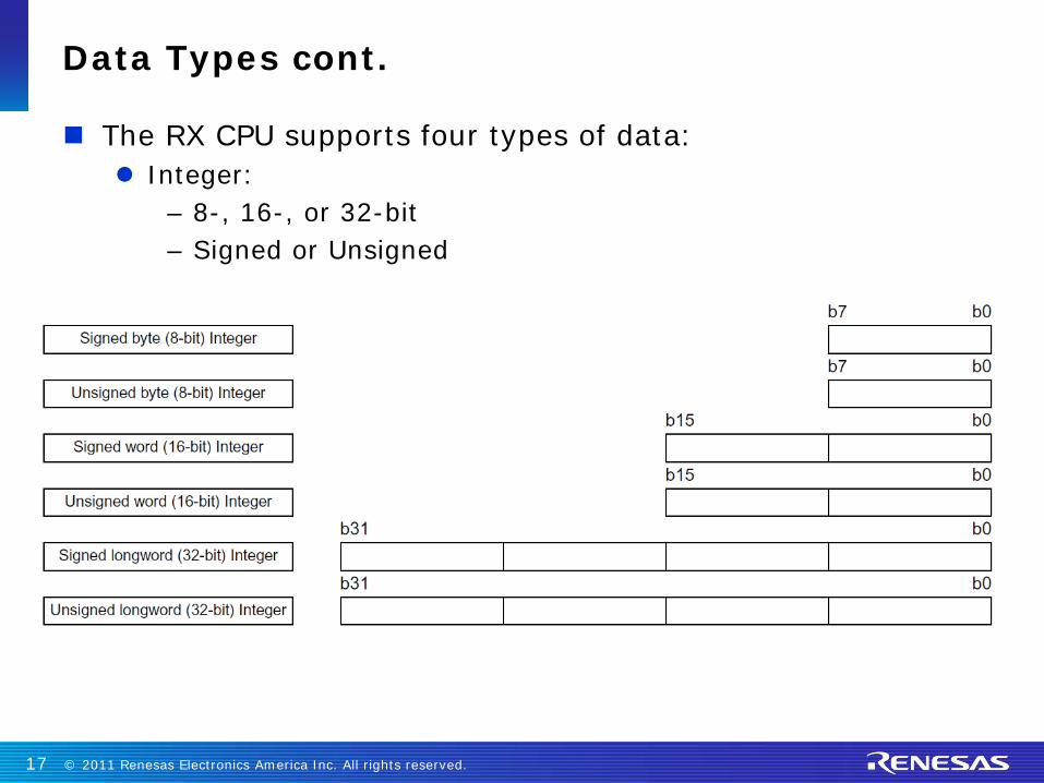
Data Types cont.
The RX CPU supports four types of data: Integer:
– 8-, 16-, or 32-bit – Signed or Unsigned
© 2011 Renesas Electronics America Inc. All rights reserved. 17

Data Types cont.
Floating-Point: – RX Family supports single precision floating-point
computation following the IEEE 754 standard – There are eight floating point operations available:
– FADD, FCMP, FDIV, FMUL, FSUB, FTOI, ITOF, and ROUND.
– Single-precision floating-point – S: Sign (1 bit) – E: Exponent (8 bits) – F: Mantissa (23 bits)
© 2011 Renesas Electronics America Inc. All rights reserved. 18
Data Types cont.
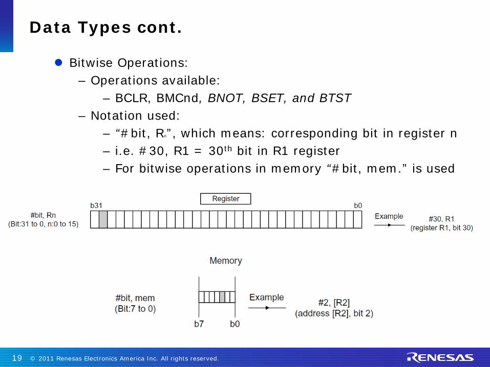
Bitwise Operations: – Operations available:
– BCLR, BMCnd, BNOT, BSET, and BTST – Notation used:
– “#bit, Rn”, which means: corresponding bit in register n – i.e. #30, R1 = 30th bit in R1 register – For bitwise operations in memory “#bit, mem.” is used
© 2011 Renesas Electronics America Inc. All rights reserved. 19

Endianness
Endianness refers to the arrangement of sub-units such as bytes within a longer data word, while storing it in memory Big endian: The most significant byte (MSB) is stored at the
lowest byte address of the memory. Little endian: The least significant byte (LSB) is stored at the
lowest address of the memory The RX63N/RX631 Group supports both big and little endian
© 2011 Renesas Electronics America Inc. All rights reserved. 20

Data Arrangement
Data Arrangement in Registers The least significant bit is the rightmost bit while the most
significant bit is the leftmost bit
© 2011 Renesas Electronics America Inc. All rights reserved. 21

Data Arrangement cont.
Data Arrangement in Memory Byte (8-bit), word (16-bit), or longword (32-bit) Different depending on whether little or big endian is used
© 2011 Renesas Electronics America Inc. All rights reserved. 22

Bus Specification
CPU bus Instruction bus and Operand bus:
– Connects the CPU to on-chip memory (RAM and ROM) – Operates in synchronization with the system clock (ICLK)
Memory bus Memory bus 1 and 2:
– Connected to the on-chip RAM Internal main bus
Internal main bus 1: – Connected to CPU
Internal main bus 2: – Connected to DMACA, DTC, EDMAC, and on-chip RAM and
ROM
© 2011 Renesas Electronics America Inc. All rights reserved. 23

Description of Buses
CPU Buses Fetches instructions for the CPU and accesses operands Programming and erasure is handles by the internal peripheral
bus Bus-access operations can proceed simultaneously, e.g. parallel
access to on-chip RAM or ROM Memory bus
Accesses on-chip ROM and RAM Internal main bus
Internal main bus 1 is used by the CPU and internal main bus 2 is used by other bus-master modules such as DTC, DMACA, and EDMAC.
Bus master priority:
© 2011 Renesas Electronics America Inc. All rights reserved. 24

Description of Buses cont.
Internal peripheral bus The table below lists the six internal peripheral buses and what
peripheral modules they are connected to
© 2011 Renesas Electronics America Inc. All rights reserved. 25

Description of Buses cont.
External Bus Arbitrates requests from the internal main bus 1, 2 and
EXDMAC and decides the master The order of priority is, from high to low:
– EXDMAC – Internal main bus 2 – Internal main bus 1
Bus Error Monitor Section Generates an interrupt whenever an error is detected on the
bus Some errors are:
– Illegal address access error – Access to areas for which operation has been disabled
– Timeout error – Happens after 768 cycles if the bus access is not
completed
© 2011 Renesas Electronics America Inc. All rights reserved. 26

Pipelining
Pipelining is an important technique used to make fast CPUs A pipeline consists of several stages which allows the
instruction throughput to increase A pipeline stage cannot be any faster than the slowest stage
If for example the execution stage takes more time than the memory access stage, then performance degrades to the slowest stage
The RX CPU is based on a five-stage pipeline: Instruction Fetch Stage (IF Stage):
– CPU fetches 32/64 bit instructions from the memory. – PC is incremented by 4 or 8 since the instructions are 4 or 8
bytes long Instruction Decode Stage (ID Stage):
– Instructions are decoded and converted into micro-operations.
© 2011 Renesas Electronics America Inc. All rights reserved. 27

Pipelining cont.
Execution Stage (E Stage): – Two types of calculations take place in this stage
– Normal ALU operations: – Add, sub, compare, and logical operations
– Memory address calculations Memory Access (M Stage):
– Memory is accessed for either fetching an operand from the memory or storing an operand in the memory.
Write-back stage (WB stage): – The last stage of the pipeline writes data into the register
file
© 2011 Renesas Electronics America Inc. All rights reserved. 28
Pipeline Operational Hazards
Ideally, each pipeline stage should take the same amount of time to process the instruction
Unfortunately, ideal conditions are hard to achieve and hence stalls are created in the pipeline and performance is degraded
Hazards prevent the next instruction from executing at the next cycle and reduce the performance of the pipeline
Structural hazard: Arises from resource conflicts when the hardware is not capable
of supporting multiple instructions simultaneously in an overlapped manner
For example a single memory that is being accessed simultaneously in both the instruction fetch stage and the memory stage
© 2011 Renesas Electronics America Inc. All rights reserved. 29

Pipeline Operational Hazards cont.
Data hazard: Arises when an instruction depends on the result of a previous
instruction, e.g.: – Instruction 1: A+B = C – Instruction 2: C+D = F – Instruction 2 cannot be executed before instruction 1 has
completed since the instruction is dependent on the value C calculated in instruction 1
Control hazard: Also known as branch hazard Arises from pipelining of branches and other instructions that
change the program counter For example, when a set of instructions are control dependent
on the branch condition, and what value the PC will take is not known until the execution stage or decode stage
© 2011 Renesas Electronics America Inc. All rights reserved. 30

Operating Modes
There are six operating modes with two types of operating-mode selections
Boot Mode:
– Provided for the flash memory – Functions the same way as single-chip mode except for data
write/erase function to the flash memory USB Boot mode:
– Provided for the flash memory – Functions the same way as single-chip mode except for data
write/erase function to the flash memory
© 2011 Renesas Electronics America Inc. All rights reserved. 31

Operating Modes cont.
Single-Chip Mode: – On-chip ROM can be set to either enabled or disabled – All I/O ports are accessible and the external bus is always
disabled
© 2011 Renesas Electronics America Inc. All rights reserved. 32

Operating Modes
The following illustration outlines the mode transitions depending on the settings of the MD and PC7 pins
© 2011 Renesas Electronics America Inc. All rights reserved. 33

Memory Organization
Byte Addressing vs. Word Addressing By using N address lines we can address 2^N distinct
addresses, numbered 0 through 2^N - 1. Logical layout of a block of memory (1)
Byte addressing (2)
Word addressing (3)
Memory Map This microcontroller has a 4-Gbyte address space, which ranges
from0000 0000h to FFFF FFFFh.
© 2011 Renesas Electronics America Inc. All rights reserved. 34
1. 2.
3.

I/O Registers
This section focuses on preventive measures that should be taken while using I/O registers
In some cases, after writing into I/O registers, you must check whether the write operation is completed
The CPU could also behave differently and could lead to unpredictable results
The correct way to handle each situation is to wait until the write operation is completed and by following these steps: Write to an I/O register. Read the value from the I/O register to a general register. Execute the operation using the value read. Execute the subsequent instruction.
© 2011 Renesas Electronics America Inc. All rights reserved. 35
What we have covered
Architecture of the Renesas RX63N CPU Specifications and Instruction Set Register Set Data Types Data Arrangement Bus Specifications Pipelining and Pipeline Hazards Operating Modes Organization of Registers and Memory How I/O Registers should be accessed
© 2011 Renesas Electronics America Inc. All rights reserved. 36

Renesas Electronics America Inc. © 2013 Renesas Electronics America Inc. All rights reserved.