optimization of the wire grid size for differential ... · optimization of the wire grid size for...
TRANSCRIPT
Microelectronics Journal 41 (2010) 669–679
Contents lists available at ScienceDirect
Microelectronics Journal
0026-26
doi:10.1
n Corr
Univers
E-m
stephan1 Te
journal homepage: www.elsevier.com/locate/mejo
Optimization of the wire grid size for differential routing: Analysis andimpact on the power-delay-area tradeoff
Massimo Alioto a,n, Stephane Badel 1,b, Yusuf Leblebici b,1
a Department of Information Engineering, University of Siena, Italyb Microelectronic Systems Laboratory, Ecole Polytechnique Federale de Lausanne, Lausanne, Switzerland
a r t i c l e i n f o
Article history:
Received 17 February 2009
Received in revised form
10 June 2010
Accepted 14 June 2010
Keywords:
Differential routing
VLSI
Optimization
Interconnects
Low power
92/$ - see front matter & 2010 Elsevier Ltd. A
016/j.mejo.2010.06.005
esponding author. Current adress: Berkeley
ity of California, Berkeley, USA.
ail addresses: [email protected], alioto@ee
[email protected] (S. Badel), yusuf.leblebici@ep
l. +41 21 693 69 22; fax: +41 21 693 69 59.
a b s t r a c t
In this paper, the impact of the wire grid size on the power-delay-area tradeoff of VLSI digital circuits
with differential routing is analyzed. To this aim, the differential MOS current-mode logic (MCML) is
adopted as reference logic style, and a complete differential design flow is used. Analysis shows that the
choice of the grid size in differential routing has a much stronger impact on the power-delay-area
tradeoff, compared to the usual single-ended case. Hence, the grid size is an important knob that must
be carefully selected when differential routing is adopted. The dependence of power, delay and area on
the grid size is discussed in detail through simple models, and introducing appropriate metrics.
To validate the analysis and show basic dependencies in practical circuits, 30 benchmark circuits with
an in-house designed MCML cell library were synthesized and routed in 0.18 mm CMOS technology.
Results show that non-optimal choice of the grid size can determine a dramatic increase in power
(1.7� ) and area (1.3� ). Interestingly, the grid size that optimizes the power-delay-area tradeoff is
almost independent of the specific circuit under design; hence a generally optimum grid size exists that
optimizes a very wide range of different circuits.
& 2010 Elsevier Ltd. All rights reserved.
1. Introduction
Interconnects heavily influence the power-delay-area tradeoffin deep-submicron VLSI digital circuits, due to the strongcontribution of their parasitics. The impact of interconnects isusually managed with automated CAD tools that performinterconnect-aware physical synthesis and place and route [1,2].Such automated design flows are usually available for single-ended logic styles, whereas differential logic styles are notexplicitly supported [3,4]. Accordingly, the adoption of differentiallogic styles requires further work to properly adapt commercialtools.
Until now, differential logic styles such as MOS current-modelogic (MCML) have been widely recognized to provide consider-able advantages in terms of power supply noise comparedto conventional CMOS logic [5]. From an application point ofview, the reduced supply noise in MCML circuits enables anumber of applications, such as digital signal processing or errorcorrection in high-accuracy mixed-signal circuits, where sub-strate noise reduction is key to improving the dynamic range of
ll rights reserved.
Wireless Research Center,
cs.berkeley.edu (M. Alioto),
fl.ch (Y. Leblebici).
noise-sensitive analog circuits. As another example, the lowsupply noise feature is very useful also in cryptographic deviceswith high level of security, since it makes differential poweranalysis (DPA) attacks much harder, thereby considerablyincreasing the level of protection of the secret key [6]. In theseapplications, the advantage offered by the MCML logic style overstandard CMOS circuits has been experimentally demonstrated tobe in the order of 2–3 orders of magnitude at least, although thiscomes at the cost of a power and area penalty [5,6]. In addition, tomake MCML a practical option for commercial chips, the designeffort has to be kept close to that of standard CMOS circuits, hencemanual design of MCML digital blocks is not a viable approach.Accordingly, the use of standard-cell based automated designmethodologies for MCML circuits is mandatory.
In differential logic styles such as MCML, each signal is carriedby a pair of wires that switch in opposite directions, thuscanceling out the power supply and substrate noise to a largeextent [5–13]. The maximum benefits are obtained when eachdifferential signal pair is routed as a bundle (usually named ‘‘fullydifferential pair’’), in which the two complementary wires haveexactly the same length [3–7,11]. Until now, a few methodologieshave been developed to allow the implementation of fullydifferential logic circuits with standard CAD tools [3–7]. In thefirst step, these methodologies rely on a fictitious single-endedrepresentation of differential signals, in order to allow for usingcommercial CAD tools. Then, in a post-processing step, the
M. Alioto et al. / Microelectronics Journal 41 (2010) 669–679670
fictitious single-ended cells and wires are turned into the fullydifferential and logically equivalent counterparts. In such meth-odologies, it was shown that timing integrity throughout all stepsof the design flow requires a fully differential routing, whichmatches the lengths and parasitic of the two wires belonging tothe same differential signal pair. In other words, the two wiresbelonging to the same pair must be always routed in parallel toeach other, as will be discussed in detail in Section 2.
As is well known, automated routing of VLSI circuits isefficiently performed by restricting the possible decisions thatthe tool can make. In particular, the tool is allowed to place androute wires only at discrete positions in the die, according to arouting grid [8,9]. In single-ended design flows, the wire grid pitch(i.e., the grid step) is often set to the minimum value allowed bythe technology in order to provide maximum integration density.Nevertheless, non-minimum wire grid pitch can bring limitedbenefits (in the order of 10%) in terms of speed and powerconsumption [10], since coupling capacitances between adjacentwires are reduced when their distance is increased. Moreover,current routing tools are able to automatically spread neighboringwires apart when routing space is available. Therefore, the choiceof the wire grid pitch is not critical in the case of single-endedrouting, and can bring only a modest improvement compared tothe case of minimum pitch.
As opposite to single-ended design flows, the impact of wiregrid pitch in differential design flows is expected to be strong,since wires belonging to the same differential pair are forced to beclose to each other by necessity, and tools are not able to freelyadjust their spacing. In addition, wires within the same pairalways experience opposite transitions, hence their effectivecoupling capacitance is always increased by a factor of two dueto the Miller effect [2,11–13]. For these reasons, the choice of thewire grid pitch is expected to be a critical design variable indifferential design flows, and further investigation is needed.
In this paper, the impact of the wire grid size in fullydifferential design flows is analyzed. In particular, the impact ofthe wire grid pitch on the power-delay-area tradeoff is analyzedin detail through simple models and design considerations,adopting a differential MOS current mode logic standard celllibrary and a previously developed fully differential design flow.Simple design metrics to optimize the grid pitch are alsointroduced. According to the above premises, our analysis isfocused on local wires that connect standard cells within the samemodule, hence effects typically associated with global wires (e.g.,wire inductance) will not be considered.2 Analysis of 30 bench-mark circuits in 0.18-mm technology is performed to validate theabove considerations. Results show that the proper choice of thewire grid pitch in differential design flows significantly reducespower and area for a given delay constraint. Interestingly, theoptimum wire grid pitch was found to be almost independent ofthe specific circuit under design, hence pitch optimization can beperformed only once and used for a large number of differentdesigns.
The paper is structured as follows. In Section 2, a completefully differential design flow is introduced. Qualitative considera-tions on the impact of the wire grid pitch and comparisonbetween differential and single-ended routing are reported inSection 3, whereas a design metric is derived in Section 4.Validation and simulation results are discussed in Section 5, andconclusions are discussed in Section 6.
2 Observe that issues related to global interconnects are completely different
from local (intra-module) interconnects both in terms of the impact of wire
parasitics and design issues. Indeed, local interconnects are mainly capacitive and
easily prone to routing congestion, whereas global wires exhibit also resistive/
inductive behavior and typically do not suffer from serious congestion [20].
2. Review of a fully differential automated design flow
In order to implement circuits based on differential logicstyles, the two wires belonging to the same differential pair mustbe routed as a bundle [3–7], i.e. they must be routed in parallel toensure that they have the same length and parasitics. This fullydifferential routing approach has obvious advantages in terms ofsignal integrity, which is an important aspect in nanometertechnologies, especially in the case of low-swing differential logicstyles with reduced noise margin [4,11]. However, the mainreason for using fully differential routing is related to timinganalysis. Indeed, in fully differential logic styles, the switching oflogic gates is triggered by the variations in the differential inputvoltage; hence the timing arcs should relate input and outputdifferential voltages during the timing analysis of the circuit.Unfortunately, current commercial timing analyzers are not ableto model timing of differential signals, as they support onlysingle-ended timing relationships.
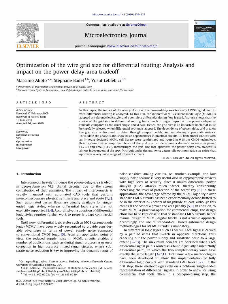
The problem is illustrated in Fig. 1, where the switching of apair of complementary signals is represented in the case ofindependently routed wires, i.e. with different length andparasitics, thereby violating the premise of fully differentialdesign flows. Because of the difference in the parasiticsassociated with each wire, the transitions of the driving gatehave different time constants. In other words, from Fig. 1 the twocomplementary signals OUT and OUT0 cross the 50% threshold atdifferent points in time, and the point in time where thedifference of the two signals crosses the 50% threshold islocated somewhere in between (in fact, it can be easily seenthat it is close to the average of the two individual points, forsmall differences of the two time constants). Therefore, if theinput-to-output delay is evaluated as the delay at only one of thetwo single-ended outputs (as allowed by current CAD tools), itunderestimates or overestimates the actual delay evaluated onthe differential waveform. These timing errors can accumulateand lead to considerable error when evaluating a path delay.Clearly, such timing errors are not acceptable in high-speedapplications, since it is likely that the speed constraint will not beactually met. Analogously, such errors are not acceptable in low-power applications, since the delay overestimation clearly leadsto a circuit overdesign, thereby degrading the power efficiency.
According to the above considerations, commercial CAD toolscan accurately estimate the delay of differential logic gates only ifthe two outputs of a differential pair have exactly the same delay.This can be achieved by balancing the parasitics of the two wires
Fig. 1. 50% crossing points for two wires belonging to the same differential pair
and the corresponding differential voltage.
M. Alioto et al. / Microelectronics Journal 41 (2010) 669–679 671
within that same pair as much as possible, i.e. routing them as abundle.
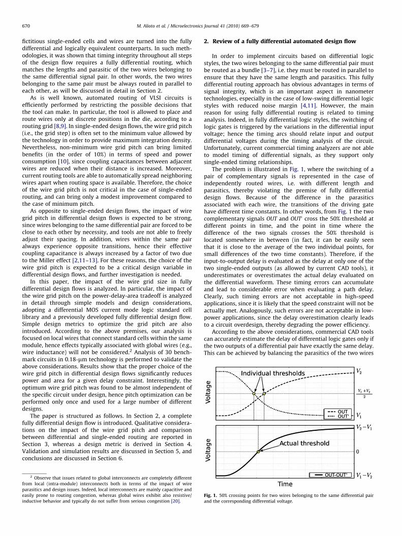
A complete fully differential design flow was recently devel-oped, based on the above discussed concept [4]. With no loss ofgenerality, in the following this design flow will be applied to astandard cell library based on MOS current-mode logic (MCML)style [14,15]. The design flow for differential MCML standard cellsis briefly illustrated in the flowchart in Fig. 2. Essentially, twodifferent views of the cell library are necessary: a logical view,where each pair of complementary signals (differential inputs andoutput of the cell) is represented as a single port, and a physicalview which includes both polarities for each signal. Once the celllayouts are created, they are characterized for timing and power.Logical and physical models are generated for simulation,
Fig. 2. Flowchart of the fully d
synthesis (timing library) and placement and routing (abstracts).Then, a number of variants are generated for each cell by invertingthe inputs and output in all possible combinations, to takeadvantage of the free signal inversion available with differentialcells (in differential cells, logic inversion is performed by simplyswapping pins).
In the circuit automated design, wire capacitance values areproperly evaluated to reflect the higher effective capacitance seenin differential wires (more details are provided in Section 3), inorder to ensure accurate timing analysis throughout the flow.Based on a standard-cell logic library and a standard HDLdescription, circuits are then synthesized, placed and routed usingstandard tools. The resulting circuit is made of fictitious single-ended cells and wires, where each wire actually represents a pair
ifferential design flow [4].

M. Alioto et al. / Microelectronics Journal 41 (2010) 669–679672
of complementary signals, according to appropriate design rulesthat accommodate for the increased wire width. Then, a scripttranslates the single-ended design into a physical equivalentdifferential design, by splitting each wire into a differential pair,and replacing each cell by its physical counterpart. To correctlyconnect each wire to the corresponding cell pins, the resultingdesign is fed back to the router to complete the connections.
Summarizing, thanks to the joint adoption of commercial CADtools and appropriate scripts, the above design flow permits theautomated design of differential digital circuits from their VHDL/Verilog description to their detailed physical-level design.
3 Actually, area may even slightly reduced by moderately increasing P. Indeed,
the reduction in Cwire allows the synthesis tool to reduce the cell strength and
hence area.
3. Understanding the impact of the routing grid pitch
When using a design flow that includes automated place androuting, the designer has to preliminarily choose the wire gridpitch. Unfortunately, until now no criteria or guidelines have beenprovided to assist this choice. For this reason, in the following theimpact of wire grid pitch is analyzed in detail for fully differentialrouting, highlighting the interdependence of fundamental designparameters, such as speed, power consumption and area.
3.1. Analysis of the power-delay-area tradeoff versus wire grid pitch
In any type of automated routing, as shown in Fig. 3 the wiregrid size is set by the pitch P, which is defined as the distancebetween the middle sections of the adjacent wires. In the samefigure, capacitance Ccoupling,INT schematizes the intrinsic couplingcapacitance between the considered wires, whereas CGND
represents the grounded capacitive contribution at each wire(i.e., the contribution of the bottom plate, as well as the fringingcapacitance to ground of the lateral faces). For a given wire width,Ccoupling,INT and CGND are proportional to the wire length L via thecapacitance per unit length ccoupling and cGND, respectively (i.e.,Ccoupling,INT¼ccouplingL, CGND¼cGNDL). Analogously, the externalcapacitance towards the adjacent wires Ccoupling,EXT in Fig. 3 isproportional to the overlap length Lov (i.e., the length of theoverlapping section of the adjacent wires) via the capacitance perunit length ccoupling (i.e., Ccoupling,EXT¼ccouplingLov). In deep-submicrontechnologies, the capacitances associated with the lateral face(i.e., Ccoupling,INT and Ccoupling,EXT) are well known to dominate overthe grounded capacitance CGND, as the lateral face area tends todown-scale slowly compared to the bottom face of wires [2].
It is useful to observe that the wires belonging to the samedifferential pair always experience opposite transitions, hence thein-between coupling capacitance Ccoupling,INT is always affected bythe full Miller effect, i.e. it can be modeled as a groundedcapacitance (in parallel to CGND) equal to 2Ccoupling,INT [11]. On theother hand, the full Miller effect takes place betweenthe considered wire and the adjacent ones only if they switch atthe same time, whereas no effect is observed if they switch indifferent points of time. Hence, the capacitive contributionbetween each wire of the differential pair and the adjacent onecan be schematized as a grounded capacitance equal toaMillerCcoupling,EXT, being aMiller the well-known Miller effectcoefficient that results to 2 if full Miller effect takes place, andis lower than 2 if this effect occurs only partially [2]. Accordingly,the overall capacitance Cwire to ground associated with each wireof a differential pair is proportional to L via the wire capacitanceper unit length cwire, according to
Cwire ¼ CGNDþCcoupling,INTþCcoupling,EXT ¼ cwireL ð1aÞ
cwire ¼ cGNDþ2ccouplingþccouplingLov
LaMiller ð1bÞ
Relationships (1a) and (1b) can be used to understand theimpact of the wire grid pitch P on the wire capacitance, which isrelated to performance and power, and area. If the grid size P issmall (i.e., close to its lower bound Pmin set by the technology),ccoupling and hence cwire tend to be very high due to the shortdistance between adjacent wires, thereby degrading speed andpower efficiency. At the same time, under low values of P, themaximum possible integration density is obtained. When P isincreased with respect to Pmin, capacitance ccoupling tends todecrease. As an example, this is shown by the plot of ccoupling
versus P/Pmin in Fig. 4, where the contribution capacitivecontributions of intermediate-level (metal 2–4) layers in0.18-mm CMOS technology is considered. This is easilyexplained by considering that an increase in P tends to spreadthe lateral faces of two adjacent wires apart, thereby reducing thecapacitance associated with the parallel plates of the capacitorCcoupling,INT. At the same time, the small increase in P does notsignificantly affect the routing density, as long as no congestionoccurs in routed wires, hence the wire length L is roughlyunaffected3 by P. Accordingly, from (1a) and (1b) the net effect ofa moderate increase in P is a reduction in Cwire, which in turnimproves both speed and power efficiency.
On the other hand, if P is strongly increased with respect toPmin, the distance between differential wires becomes so high thatthe routing density is severely degraded and routing congestionoccurs. Due to congestion, wires follow longer paths thannecessary, hence their length L tends to rapidly increase whenincreasing P. Hence, despite of the small reduction in cwire (sinceccouplingp1/P slowly reduces for high values of P), the fast increasein L determines an increase of Cwire, according to (1a) and (1b).This effect is further emphasized for high values of P, as theincrease in Cwire forces the synthesis tool to increase the cellstrength for a targeted speed, which in turn further increases thecircuit area and hence the wire length.
The above discussed dependence of Cwire on the pitch P issummarized in Fig. 5, from which it is apparent that there is anoptimum grid size Popt that minimizes Cwire. Observe that thisoptimum choice of grid size improves speed and power at thesame time, and can also slightly reduce the area occupied bythe circuit (as was observed in note 1). In other words, speed,power and area are not conflicting requirements in the optimumchoice of the grid size P: indeed, the optimum grid size improvesthe routing efficiency, thereby bringing benefits to speed, powerand area at the same time.
3.2. Single-ended and differential routing: qualitative considerations
and differences
Until now, some results have been published on the impact ofthe wire pitch only in the case of single-ended routing [10,16–18].In particular, at the best of the authors’ knowledge, only [10]explicitly discusses the optimization of the wire grid pitch hereinconsidered. More specifically, [10] shows that an optimum pitchexists, and a modest improvement in power consumption andperformance can be achieved (within 10%). Moreover, theoptimum pitch is shown to significantly depend on the specificcircuit under design. On the other hand, papers [16–18] do notexplicitly consider the wire grid pitch optimization, but theytarget the design of interconnect hierarchy at the process level,and propose guidelines to select geometrical dimensions ofwires. Results in these papers agree well with the qualitative

Fig. 3. Cross section of a differential pair of wires (dark grey) and two adjacent wires (light grey).
Fig. 4. Capacitance contributions per unit length as a function of the routing pitch
P normalized to the minimum allowed by technology Pmin.
4 Indeed, CAD tools try to avoid long wires running in parallel, hence the
overlap length Lov in Fig. 3 is usually kept much lower than the wire length L.
M. Alioto et al. / Microelectronics Journal 41 (2010) 669–679 673
considerations reported in the previous subsection, but they donot provide any information on how to size the wire grid pitch indifferential routing, once the process is defined.
In general, it is expected that fully differential routing can alsotake advantage of the wire grid pitch optimization, although nowork in the literature has been devoted to this particular caseuntil now. To understand the differences with respect to thesingle-ended case, let us observe that the intrinsic couplingcapacitance (i.e., the second term in (1b)) dominates over theexternal coupling capacitance (i.e., the third term in (1b)), sinceLov5L in well-designed circuits.4 Physically, this is because theexternal contribution is due only to the generally short overlapbetween adjacent wires belonging to different pairs, whereas theintrinsic contribution has the largest possible value (since everywire within a differential pair runs parallel to the complementarywire for its entire length). Interestingly, the intrinsic contributionis constant in the design since ccoupling depends only on theprocess, whereas the external contribution depends on ratio Lov/L,which clearly depends on the specific design. Since the lattercontribution is negligible, it is expected that the wire capacitanceper unit length in differential routing is almost design-indepen-dent; hence the wire grid pitch optimization impacts thecapacitance of all wires almost in the same way, regardless ofthe considered design. In other words, the wire grid pitchoptimization is expected to be almost unaffected by the specific

grid pitch P
Cwire(eq. (1b))
L const., high cwirehigh Cwire
PoptPmin
high L, cwire const.high Cwire
min. Cwire
low performancepower inefficient
low performancepower inefficient
high performancepower efficient
Fig. 5. Dependence of Cwire on the wire pitch P.
M. Alioto et al. / Microelectronics Journal 41 (2010) 669–679674
design, i.e. a design-independent optimum pitch can be found.This qualitative result will be shown to agree well with simulationresults in Section 5.
From the above considerations, the intrinsic contribution indifferential routing is significantly greater than that of single-ended wires, whereas the grounded contribution (i.e., cGND in (1b))is almost the same in both cases. Hence, the reduction of ccoupling
obtained with the pitch increase (see Fig. 5) has a stronger effecton cwire when considering differential routing. Hence, the power/delay improvement achieved with the pitch optimization indifferential routing is expected to be much greater than that ofsingle-ended wires. This consideration will also be validatedthrough comparison with simulations in Section 5.
Summarizing, the wire grid pitch optimization in differentialcircuits is expected to significantly impact the power-delay-areatradeoff, and the resulting optimum pitch is expected to beroughly design-independent, in contrast to previous results onsingle-ended routing.
Fig. 6. Plot of FOM in (2) normalized to the case P¼Pmin versus P/Pmin for various
values of i (differential and single-ended routing).
4. Metrics to estimate the impact of grid size
As discussed in Section 3, a tradeoff between the wirecapacitance Cwire and area exists in the choice of the wire gridpitch P. In the following, simple metrics that provide informationon this tradeoff are discussed.
A reasonable metric that can express the capacitance–areatradeoff should include the product of capacitance and area, or apower of them if we want to put more weight on one of them.To achieve a general metric that permits to find the optimum wiregrid pitch Popt that leads to the best capacitance–area tradeoff(see Fig. 5), it is sufficient to derive a simple expression ofcapacitance and area that is valid for P lower than (or comparableto) the optimum pitch Popt, according to Fig. 5. As was discussed inSection 3.1, in Fig. 4, for PrPopt the wire length L is roughlyconstant, hence the dependence of Cwire on P in (1) is approximatelydue only to factor cwire. In regard to area, from Fig. 3 the areaoccupied by a pair of differential wires is proportional to the gridpitch P and wire length L, the latter of which can be again assumedto be approximately independent of P when evaluating Popt.According to these considerations, the dependence of the capaci-tance (area) on P is simply captured by cwire (P). Hence, a suitablemetric to describe the capacitance-are tradeoff is ci
wireP, whereexponent i is set to a value greater (lower) than unit if capacitance ismore (less) important than area. In this regard, observe the wire areain the region of interest where PrPopt is not a serious issue, sincefrom Fig. 5 the wire length is independent of P, whereas reduction incwire is crucial. For this reason, more weight should be put oncapacitance in the capacitance-area metric. This can be done by
introducing an exponent i¼2 in the term cwire, thereby yielding thefollowing capacitance-area figure of merit (FOM)
FOM¼ c2wireP ð2Þ
In (2), the dependence of the wire capacitance per unit lengthcwire on P can be easily extracted from technology data or fromsimulations on 3-D field solvers [2]. For example, the dependenceof cwire on P is shown in Fig. 4 for the considered 0.18 mm CMOStechnology, which has Pmin¼0.72 mm, and cwire¼0.24 fF/mm(0.19 fF/mm) for the differential (single-ended) routing underP¼Pmin (this difference is due to the additional couplingcapacitance contribution between the differential wire pair).
The resulting metric in (2) is plotted in Fig. 6 versus P/Pmin forthe differential and single-ended routing case. In this figure, cwire
and P are normalized to the values obtained for the minimum gridsize Pmin allowed by the technology. Fig. 6 reveals that thedifferential routing can provide significantly higher benefits frompitch optimization, compared to single-ended routing. Thisobservation confirms that the optimization of P is crucial indifferential routing, and agrees well with qualitative considerationsthat are reported in Section 3.2.

M. Alioto et al. / Microelectronics Journal 41 (2010) 669–679 675
Inspection of Fig. 6 also shows that the figure of merit in (2) forthe differential routing has a slightly flat minimum between1.5Pmin and 1.6Pmin, hence it is reasonable to set P to Popt¼1.5Pmin
in circuits implemented with the considered technology. This flatminimum around Popt ensures that designs around the optimumgrid pitch are robust against moderate process variations.In Section 5, it will be shown that this value of Popt agrees wellwith the optimum found experimentally in several designs.
Finally, it is interesting to compare results obtained for thedifferential routing with the single-ended case. From Fig. 6, FOM
under single-ended routing is apparently less sensitive to P,i.e. the choice of the grid size in differential routing is more criticalthan in the single-ended case. This is due to the increasedcoupling capacitance associated with each differential wire pair,as discussed in Section 3.1, and agrees well with the qualitativeconsiderations in Section 3.2. For the same reason, Popt for single-ended routing is lower than that of differential case (PoptE1.2Pmin
from Fig. 6), and is close to the minimum value allowed bytechnology.
5. Analysis of test circuits and validation
In order to evaluate the impact of routing grid size P on thepower-delay-area tradeoff, 30 circuits (ISCAS 85 and 89) takenfrom the IWLS’2005 benchmark suite [19] were synthesizedunder different values of the grid pitch. The considered bench-marks are summarized in the first column of Tables 1–3.
Each test circuit was synthesized using Synopsys DesignCompiler Topographical, which performs logic synthesisand physical optimization according to the wire technology
Table 1Summary of results for 1� delay constraint.
Design\pitch (lm) Critical path length Area
0.72 0.80 0.88 0.96 1.04 1.12 1.20 0.72 0.80 0
s27 1.00 0.94 0.94 0.94 0.89 0.89 0.92 1.00 1.09 1
s208_1 1.00 1.12 1.02 0.93 1.07 1.02 0.98 1.00 0.85 0
s298 1.00 0.96 0.89 0.92 0.89 0.90 0.89 1.00 0.86 0
s349 1.00 0.96 0.98 1.01 0.96 1.01 1.00 1.00 0.80 0
s344 1.00 0.96 0.92 0.96 0.89 0.93 0.94 1.00 0.88 0
s386 1.00 0.99 0.97 0.95 0.93 0.95 0.99 1.00 0.87 0
s420_1 1.00 0.98 0.91 0.90 0.91 0.91 0.90 1.00 1.04 0
s713 1.00 0.95 0.86 0.83 0.84 0.85 0.89 1.00 1.10 1
s526n 1.00 1.01 0.99 1.00 0.96 0.96 0.98 1.00 0.96 0
s400 1.00 1.01 0.92 0.96 0.90 0.91 0.91 1.00 0.74 0
s526 1.00 0.90 0.98 0.91 0.90 0.90 0.96 1.00 0.85 0
s382 1.00 0.98 0.96 0.97 0.99 0.97 0.99 1.00 0.94 0
s444 1.00 0.94 0.95 0.92 0.93 0.92 0.95 1.00 0.65 0
s510 1.00 1.02 0.99 1.00 1.00 0.99 1.00 1.00 0.96 0
s641 1.00 1.06 1.00 1.01 0.98 0.98 1.02 1.00 0.86 1
s820 1.00 0.99 1.00 0.99 1.00 1.00 1.00 1.00 0.74 0
s832 1.00 0.99 0.99 0.99 0.97 0.99 0.98 1.00 0.90 0
s1238 1.00 0.98 1.06 0.96 0.89 1.00 1.05 1.00 0.93 0
s838_1 1.00 0.91 0.90 0.92 0.91 0.90 0.91 1.00 0.74 0
s1196 1.00 0.89 0.91 0.81 0.85 0.90 0.81 1.00 0.87 0
s1488 1.00 0.92 0.90 0.89 0.90 0.89 0.90 1.00 0.83 0
s1494 1.00 1.01 1.01 1.02 1.02 1.02 1.02 1.00 0.82 0
s1423 1.00 0.99 1.01 1.00 1.00 1.01 1.00 1.00 0.83 0
s5378 1.00 1.02 1.04 1.12 1.01 1.05 1.00 1.00 0.68 0
s9234_1 1.00 0.85 0.76 0.80 0.75 0.81 0.78 1.00 1.00 0
s13207 1.00 1.02 0.95 0.90 0.84 0.87 0.96 1.00 0.91 0
s15850 1.00 0.98 1.04 0.99 1.00 0.99 0.88 1.00 0.91 0
s38417 1.00 0.79 0.74 0.70 0.72 0.61 0.68 1.00 0.96 0
s38584 1.00 0.81 0.86 0.79 0.79 0.80 0.89 1.00 0.91 0
s35932 1.00 0.87 0.82 0.74 0.81 0.84 0.96 1.00 0.91 0
Average 1.00 0.96 0.94 0.93 0.92 0.93 0.94 1.00 0.88 0Std. dev. 0.00 0.07 0.08 0.09 0.08 0.09 0.08 0.00 0.11 0
parameters. Routing was performed using Metal-1 to Metal-4layers. Each circuit was synthesized under several speed con-straints in order to validate the results for different performancetargets. To this end, each circuit was preliminarily characterizedto obtain the minimum delay by performing five synthesis runs(with minimum grid size Pmin), starting with very tight timingconstraints, and updating the timing constraint for the next runwith the result of the previous one. This allowed for obtaining thevery minimum delay achievable in the critical path. Then, in orderto evaluate the impact of the routing grid at different speedconstraints, synthesis runs were then performed for a delayconstraint of 1� , 1.25� , 1.5� , 2� and 5� greater than theminimum value, and with interconnect parasitic data correspond-ing to the various routing grid pitches adopted (ranging from Pmin
to 1.7Pmin). For each of these circuits and for each speedconstraint, power and area were also evaluated. The resultingvalues of the critical path delay, area and power normalized to thecase with minimum pitch are reported in Tables 1–3, whichrespectively refer to the case of 1� , 2� and 5� delay constraint.
To summarize the results in Tables 1–3, the average powerconsumption mPower (normalized to the case P¼Pmin) among theconsidered designs was evaluated to have an idea on the typicalpower saving obtained with pitch optimization. Analogously, thestandard deviation of the power consumption sPower wasevaluated to evaluate the typical spread of the power savingamong different designs. Analogous parameters mArea and sArea
were evaluated for area. Fig. 7a and b depicts mPower (mArea) underthe 1� delay constraint, as well as the typical rangemPower7sPower (mArea7sArea) indicated in light grey. Figs. 8a–band 9a–b depict the same curves for a 2� and 5� delayconstraint, respectively.
Power
.88 0.96 1.04 1.12 1.20 0.72 0.80 0.88 0.96 1.04 1.12 1.20
.12 1.00 0.94 0.94 0.94 1.00 1.07 1.14 1.00 0.81 0.83 0.79
.95 0.82 0.92 0.84 0.87 1.00 0.80 0.94 0.79 0.90 0.78 0.82
.76 0.81 0.98 0.85 0.84 1.00 0.84 0.65 0.73 0.93 0.79 0.82
.64 0.69 0.65 0.63 0.69 1.00 0.70 0.52 0.59 0.48 0.46 0.57
.92 0.77 0.76 0.75 0.75 1.00 0.85 0.89 0.70 0.69 0.64 0.68
.76 0.65 0.70 0.58 0.66 1.00 0.90 0.70 0.56 0.61 0.50 0.59
.96 0.96 0.83 0.89 0.96 1.00 1.07 0.94 0.94 0.73 0.82 0.94
.33 1.07 0.95 1.06 0.90 1.00 1.11 1.40 0.99 0.86 0.97 0.82
.75 0.73 0.69 0.88 0.87 1.00 0.93 0.65 0.60 0.56 0.81 0.83
.88 0.73 0.64 0.67 0.86 1.00 0.68 0.82 0.61 0.47 0.51 0.81
.85 0.76 0.75 0.77 0.95 1.00 0.78 0.77 0.67 0.59 0.66 0.89
.71 0.76 0.73 0.67 0.78 1.00 0.94 0.60 0.64 0.59 0.50 0.70
.74 0.71 0.77 0.66 0.71 1.00 0.53 0.65 0.56 0.66 0.54 0.61
.81 0.85 0.74 0.78 0.78 1.00 0.96 0.77 0.82 0.65 0.71 0.72
.06 0.84 0.76 0.80 0.78 1.00 0.85 1.01 0.76 0.67 0.76 0.67
.63 0.71 0.70 0.68 0.66 1.00 0.65 0.48 0.62 0.62 0.58 0.55
.79 0.56 0.72 0.72 0.72 1.00 0.86 0.73 0.44 0.62 0.63 0.62
.81 0.79 0.81 0.74 0.70 1.00 0.85 0.71 0.64 0.68 0.62 0.55
.71 0.80 0.62 0.69 0.67 1.00 0.63 0.61 0.72 0.45 0.59 0.55
.76 0.68 0.79 0.73 0.70 1.00 0.83 0.67 0.55 0.67 0.62 0.55
.81 0.74 0.68 0.79 0.66 1.00 0.77 0.74 0.67 0.58 0.71 0.57
.71 0.67 0.59 0.70 0.64 1.00 0.78 0.61 0.56 0.47 0.61 0.52
.75 0.79 0.71 0.75 0.65 1.00 0.70 0.63 0.73 0.54 0.60 0.47
.70 0.72 0.70 0.65 0.66 1.00 0.55 0.58 0.59 0.57 0.51 0.51
.83 0.86 0.82 0.83 0.87 1.00 1.00 0.73 0.77 0.70 0.71 0.78
.90 0.89 0.87 0.87 0.85 1.00 0.85 0.81 0.75 0.74 0.75 0.72
.87 0.88 0.87 0.86 0.85 1.00 0.87 0.77 0.77 0.76 0.74 0.72
.95 0.88 0.89 0.89 0.90 1.00 0.95 0.92 0.80 0.80 0.81 0.81
.83 0.78 0.78 0.77 0.79 1.00 0.84 0.69 0.60 0.61 0.57 0.62
.80 0.84 0.82 0.89 0.83 1.00 0.80 0.67 0.74 0.70 0.78 0.66
.84 0.79 0.77 0.78 0.78 1.00 0.83 0.76 0.70 0.66 0.67 0.68
.15 0.11 0.10 0.11 0.10 0.00 0.14 0.19 0.13 0.12 0.12 0.13
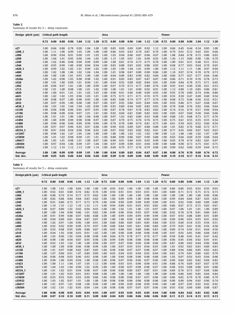
Table 2Summary of results for 2� delay constraint.
Design \pitch (lm) Critical path length Area Power
0.72 0.80 0.88 0.96 1.04 1.12 1.20 0.72 0.80 0.88 0.96 1.04 1.12 1.20 0.72 0.80 0.88 0.96 1.04 1.12 1.20
s27 1.00 0.84 0.88 0.78 0.99 1.04 1.00 1.00 0.85 0.69 0.69 0.69 0.92 1.12 1.00 0.66 0.45 0.44 0.34 0.85 1.08
s208_1 1.00 1.11 1.06 0.99 1.05 1.09 1.00 1.00 0.86 0.93 0.83 0.79 0.87 0.79 1.00 0.79 0.91 0.72 0.65 0.81 0.66
s386 1.00 0.96 0.94 0.91 0.99 1.01 1.03 1.00 1.03 0.94 0.96 0.87 0.96 0.97 1.00 1.08 0.84 0.78 0.72 0.80 0.93
s298 1.00 1.04 1.01 0.95 0.96 1.04 1.05 1.00 1.15 1.05 0.91 1.01 0.99 0.93 1.00 1.36 1.15 0.80 0.98 1.06 0.79
s349 1.00 1.02 0.96 0.98 0.99 0.99 0.99 1.00 1.00 0.81 0.76 0.75 0.75 0.78 1.00 1.00 0.61 0.51 0.48 0.51 0.53
s344 1.00 0.95 0.99 1.00 0.90 0.94 0.94 1.00 0.83 0.88 0.83 0.83 0.88 0.85 1.00 0.68 0.77 0.63 0.64 0.70 0.65
s420_1 1.00 0.99 1.02 1.02 1.01 0.99 1.02 1.00 1.05 1.09 1.04 1.01 0.99 1.00 1.00 1.12 1.11 1.11 1.06 0.97 0.94
s400 1.00 1.02 1.08 1.06 1.02 1.04 1.04 1.00 1.01 0.98 0.87 0.89 0.90 0.86 1.00 1.10 0.97 0.74 0.78 0.79 0.73
s444 1.00 1.00 1.00 1.01 0.93 1.00 1.00 1.00 0.94 0.89 0.83 0.90 0.82 0.84 1.00 0.86 0.77 0.67 0.77 0.64 0.68
s526n 1.00 1.02 0.98 1.03 0.98 0.98 1.02 1.00 0.91 0.85 0.85 0.87 0.87 0.87 1.00 0.86 0.71 0.70 0.76 0.78 0.73
s526 1.00 1.01 1.00 0.99 1.01 0.99 1.01 1.00 0.94 0.93 0.90 0.85 0.84 0.81 1.00 0.90 0.84 0.78 0.75 0.71 0.65
s382 1.00 0.96 0.97 1.01 1.00 1.00 0.99 1.00 0.97 0.70 0.73 0.77 0.80 0.76 1.00 0.93 0.43 0.49 0.58 0.61 0.53
s713 1.00 1.01 1.00 0.98 1.00 1.01 1.02 1.00 1.06 1.01 1.01 0.90 0.92 0.91 1.00 1.12 0.89 1.10 0.85 0.86 0.81
s820 1.00 1.00 0.91 1.01 1.01 1.02 1.03 1.00 0.98 0.91 0.96 0.90 0.99 0.95 1.00 0.95 0.78 0.89 0.74 0.96 0.86
s641 1.00 1.02 1.02 1.03 0.96 1.03 1.01 1.00 0.75 0.73 0.71 0.71 0.76 0.75 1.00 0.55 0.50 0.47 0.49 0.60 0.54
s510 1.00 0.98 0.97 1.00 0.98 0.95 1.00 1.00 0.85 0.86 0.74 0.77 0.77 0.76 1.00 0.68 0.72 0.48 0.56 0.52 0.51
s832 1.00 0.97 0.99 1.00 0.98 1.00 0.97 1.00 0.97 0.92 0.86 0.83 0.84 0.83 1.00 0.93 0.86 0.71 0.67 0.68 0.67
s838_1 1.00 1.03 1.02 1.04 1.04 1.02 0.99 1.00 0.93 0.89 0.94 0.85 0.82 0.83 1.00 0.78 0.68 0.76 0.65 0.66 0.64
s1238 1.00 0.96 0.98 0.96 0.95 0.97 0.95 1.00 0.87 0.78 0.87 0.78 0.83 0.82 1.00 0.74 0.55 0.76 0.57 0.66 0.64
s1196 1.00 0.98 0.98 0.94 0.97 1.01 1.01 1.00 0.92 0.84 0.81 0.80 0.82 0.83 1.00 0.85 0.67 0.60 0.58 0.66 0.66
s1423 1.00 1.01 1.01 1.00 1.00 1.04 0.98 1.00 0.97 1.03 0.85 0.89 0.93 0.88 1.00 0.88 1.01 0.68 0.73 0.77 0.76
s1494 1.00 1.00 0.99 0.99 0.98 0.98 0.97 1.00 0.87 0.79 0.75 0.76 0.76 0.75 1.00 0.75 0.61 0.55 0.55 0.55 0.54
s1488 1.00 0.99 0.98 0.99 0.99 0.99 0.99 1.00 0.79 0.78 0.80 0.74 0.81 0.75 1.00 0.61 0.59 0.63 0.52 0.66 0.54
s5378 1.00 0.97 0.97 0.96 0.95 0.97 0.98 1.00 0.99 0.92 0.89 0.87 0.88 0.88 1.00 1.01 0.82 0.76 0.68 0.72 0.71
s9234_1 1.00 0.97 0.94 0.94 0.96 0.96 0.92 1.00 0.87 0.82 0.83 0.82 0.82 0.81 1.00 0.77 0.65 0.66 0.67 0.63 0.63
s13207 1.00 0.96 1.02 1.07 1.05 1.04 1.06 1.00 1.06 1.00 1.02 1.01 1.02 1.00 1.00 1.21 1.00 1.06 1.02 1.07 1.00
s15850 1.00 1.01 1.02 0.98 0.99 1.01 1.01 1.00 0.88 0.89 0.86 0.87 0.90 0.88 1.00 0.65 0.66 0.60 0.59 0.68 0.64
s38417 1.00 1.03 1.01 0.98 1.01 1.00 0.97 1.00 0.99 0.91 0.89 0.93 0.92 0.99 1.00 0.95 0.78 0.74 0.83 0.81 0.97
s38584 1.00 0.97 0.94 1.06 0.99 1.07 1.04 1.00 0.97 0.99 0.90 0.91 0.94 0.90 1.00 0.88 0.90 0.73 0.75 0.81 0.75
s35932 1.00 1.12 1.16 1.12 1.13 1.09 1.14 1.00 0.96 0.79 0.77 0.76 0.79 0.88 1.00 0.90 0.62 0.60 0.59 0.64 0.73
Average 1.00 1.00 0.99 0.99 0.99 1.01 1.00 1.00 0.94 0.89 0.85 0.84 0.87 0.87 1.00 0.88 0.76 0.70 0.69 0.74 0.72Std. dev. 0.00 0.05 0.05 0.06 0.04 0.04 0.04 0.00 0.09 0.10 0.09 0.08 0.08 0.09 0.00 0.19 0.18 0.17 0.16 0.14 0.15
Table 3Summary of results for 5� delay constraint.
Design\pitch (lm) Critical path length Area Power
0.72 0.80 0.88 0.96 1.04 1.12 1.20 0.72 0.80 0.88 0.96 1.04 1.12 1.20 0.72 0.80 0.88 0.96 1.04 1.12 1.20
s27 1.00 1.08 1.01 1.00 0.84 1.00 1.00 1.00 0.92 0.92 1.00 1.00 1.00 1.00 1.00 0.86 0.86 0.93 0.93 0.93 0.93
s208_1 1.00 0.92 0.81 0.80 0.76 0.82 0.76 1.00 0.94 0.91 0.91 0.93 0.91 0.91 1.00 0.80 0.71 0.72 0.75 0.72 0.73
s386 1.00 0.88 0.79 0.74 0.77 0.75 0.82 1.00 1.00 1.00 1.00 1.00 1.00 1.00 1.00 1.00 1.00 1.00 1.00 0.96 0.96
s298 1.00 0.82 0.88 0.84 0.84 0.83 0.82 1.00 1.00 0.99 0.99 1.00 0.98 0.98 1.00 0.99 0.84 0.84 0.87 0.83 0.83
s349 1.00 0.91 0.80 0.75 0.77 0.73 0.79 1.00 0.99 0.99 0.99 0.99 0.99 0.99 1.00 0.91 0.92 0.90 0.89 0.89 0.89
s344 1.00 1.19 1.35 1.22 1.16 1.32 1.11 1.00 0.94 0.89 0.91 0.93 0.93 0.85 1.00 0.86 0.67 0.75 0.72 0.83 0.67
s420_1 1.00 0.97 0.89 1.02 0.92 0.94 0.93 1.00 1.00 1.02 1.01 1.00 1.01 0.97 1.00 0.97 1.06 1.01 1.01 1.00 0.89
s444 1.00 1.00 1.04 0.90 0.86 1.01 0.82 1.00 0.99 0.96 0.94 0.95 0.97 0.96 1.00 0.92 0.78 0.78 0.81 0.86 0.81
s526n 1.00 0.91 0.99 0.88 0.97 0.86 0.88 1.00 1.00 0.99 0.99 0.99 0.99 0.99 1.00 0.97 0.93 0.88 0.89 0.91 0.89
s526 1.00 0.94 0.89 0.81 0.84 0.87 0.87 1.00 1.00 1.00 0.99 1.00 0.99 0.99 1.00 0.99 0.96 0.93 0.93 0.91 0.92
s382 1.00 1.02 0.97 1.04 0.96 1.00 0.91 1.00 0.86 0.86 0.85 0.85 0.85 0.84 1.00 0.55 0.60 0.54 0.55 0.56 0.51
s400 1.00 0.92 0.92 0.99 0.99 0.79 0.97 1.00 0.88 0.84 0.81 0.81 0.80 0.80 1.00 0.79 0.65 0.61 0.56 0.56 0.58
s713 1.00 0.93 0.98 0.95 0.99 0.88 0.87 1.00 0.95 0.90 0.81 0.80 0.86 0.83 1.00 0.89 0.74 0.56 0.51 0.64 0.56
s510 1.00 0.94 1.03 0.96 0.93 0.91 1.02 1.00 1.00 0.98 0.98 0.98 0.98 0.98 1.00 0.97 0.92 0.85 0.86 0.84 0.83
s641 1.00 1.02 0.96 1.02 0.94 0.98 0.98 1.00 0.84 0.79 0.78 0.77 0.79 0.77 1.00 0.58 0.48 0.45 0.41 0.47 0.42
s820 1.00 0.98 1.00 0.94 0.87 0.95 0.96 1.00 0.99 0.99 0.98 0.98 0.98 0.98 1.00 0.96 0.95 0.94 0.92 0.91 0.91
s832 1.00 0.92 1.03 1.02 1.00 1.00 0.98 1.00 0.97 0.97 0.96 0.96 0.98 0.96 1.00 0.87 0.88 0.83 0.84 0.96 0.86
s838_1 1.00 1.00 1.00 0.98 0.96 0.98 0.99 1.00 1.00 0.97 0.93 0.93 0.94 0.93 1.00 1.01 0.92 0.83 0.83 0.89 0.83
s1238 1.00 1.01 0.97 0.88 0.82 0.87 0.85 1.00 0.98 0.98 0.97 0.97 0.96 0.97 1.00 0.88 0.94 0.86 0.85 0.83 0.83
s1196 1.00 1.07 0.96 0.91 1.07 0.89 0.89 1.00 0.95 0.94 0.95 0.94 0.95 0.94 1.00 0.81 0.79 0.81 0.80 0.82 0.79
s1494 1.00 0.96 0.98 0.93 0.96 0.93 0.98 1.00 1.00 0.99 0.98 0.98 0.98 0.98 1.00 1.03 0.97 0.93 0.93 0.94 0.96
s1488 1.00 0.98 1.00 0.94 0.94 1.00 0.98 1.00 0.98 0.97 0.96 0.96 0.97 0.96 1.00 0.90 0.84 0.82 0.82 0.84 0.82
s1423 1.00 1.00 1.11 1.04 1.07 1.05 1.12 1.00 0.96 0.93 0.91 0.90 0.90 0.91 1.00 0.88 0.76 0.69 0.67 0.67 0.70
s5378 1.00 1.04 1.03 1.04 0.99 1.02 0.99 1.00 1.00 0.98 0.97 0.98 0.98 0.97 1.00 0.98 0.93 0.88 0.88 0.91 0.88
s9234_1 1.00 1.01 1.02 0.91 0.94 0.98 0.97 1.00 0.96 0.90 0.89 0.87 0.87 0.91 1.00 0.89 0.76 0.73 0.67 0.69 0.80
s13207 1.00 1.01 1.02 0.93 0.91 0.93 0.88 1.00 1.00 1.00 1.00 1.00 1.00 1.00 1.00 0.98 0.86 0.85 0.85 0.84 0.84
s15850 1.00 0.95 0.93 0.95 0.93 0.99 0.86 1.00 0.98 0.98 0.98 0.97 0.97 0.98 1.00 0.86 0.82 0.79 0.78 0.80 0.79
s35932 1.00 1.03 1.02 0.97 1.01 1.00 1.00 1.00 0.98 0.98 0.98 0.98 0.98 0.98 1.00 0.90 0.90 0.94 0.92 0.90 0.74
s38417 1.00 1.01 0.97 1.01 0.98 1.00 0.96 1.00 1.00 0.99 0.99 0.98 0.99 0.99 1.00 1.00 0.97 0.95 0.92 0.92 0.92
s38584 1.00 1.02 1.01 1.02 0.95 0.94 1.04 1.00 0.98 0.98 0.97 0.97 0.97 0.96 1.00 0.93 0.92 0.90 0.89 0.88 0.87
Average 1.00 0.98 0.98 0.95 0.93 0.94 0.93 1.00 0.97 0.95 0.95 0.95 0.95 0.94 1.00 0.90 0.84 0.82 0.81 0.82 0.80Std. dev. 0.00 0.07 0.10 0.10 0.09 0.11 0.09 0.00 0.04 0.05 0.06 0.06 0.06 0.06 0.00 0.11 0.13 0.14 0.15 0.13 0.13
M. Alioto et al. / Microelectronics Journal 41 (2010) 669–679676
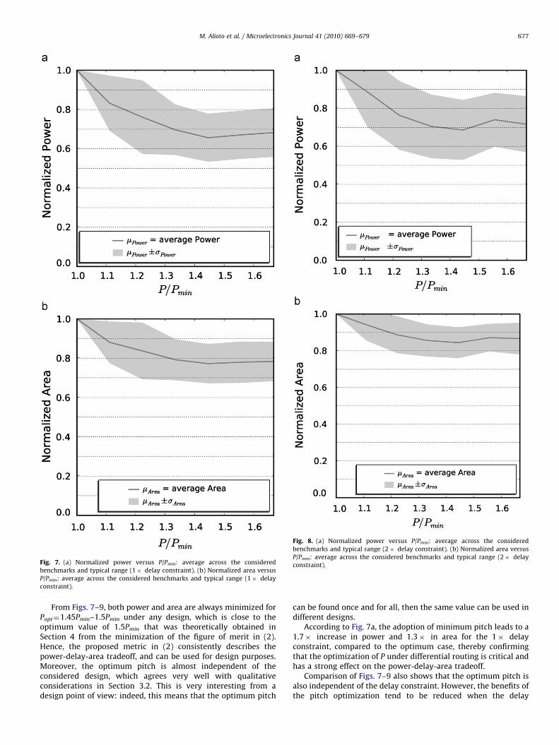
Fig. 7. (a) Normalized power versus P/Pmin: average across the considered
benchmarks and typical range (1� delay constraint). (b) Normalized area versus
P/Pmin: average across the considered benchmarks and typical range (1� delay
constraint).
Fig. 8. (a) Normalized power versus P/Pmin: average across the considered
benchmarks and typical range (2� delay constraint). (b) Normalized area versus
P/Pmin: average across the considered benchmarks and typical range (2� delay
constraint).
M. Alioto et al. / Microelectronics Journal 41 (2010) 669–679 677
From Figs. 7–9, both power and area are always minimized forPopt¼1.45Pmin–1.5Pmin under any design, which is close to theoptimum value of 1.5Pmin that was theoretically obtained inSection 4 from the minimization of the figure of merit in (2).Hence, the proposed metric in (2) consistently describes thepower-delay-area tradeoff, and can be used for design purposes.Moreover, the optimum pitch is almost independent of theconsidered design, which agrees very well with qualitativeconsiderations in Section 3.2. This is very interesting from adesign point of view: indeed, this means that the optimum pitch
can be found once and for all, then the same value can be used indifferent designs.
According to Fig. 7a, the adoption of minimum pitch leads to a1.7� increase in power and 1.3� in area for the 1� delayconstraint, compared to the optimum case, thereby confirmingthat the optimization of P under differential routing is critical andhas a strong effect on the power-delay-area tradeoff.
Comparison of Figs. 7–9 also shows that the optimum pitch isalso independent of the delay constraint. However, the benefits ofthe pitch optimization tend to be reduced when the delay

Fig. 9. (a) Normalized power versus P/Pmin: average across the considered
benchmarks and typical range (5� delay constraint). (b) Normalized area versus
P/Pmin: average across the considered benchmarks and typical range (5� delay
constraint).
M. Alioto et al. / Microelectronics Journal 41 (2010) 669–679678
constraint is relaxed. Indeed, the power (area) under the optimumpitch is reduced by 20–45% (10–30%) when 1� or 2� delayconstraint is assumed, compared to the minimum-pitch case. Thepower (area) saving reduces to 5–35% (less than 10%) whenconsidering the 5� delay constraint. This means that the pitchoptimization is effective in reducing power and area for realisticcases where a high or moderate performance is required, whereasit is less advantageous in designs with very loose delay constraint.This can be intuitively explained by observing that, tight delayconstraints force the synthesis tool to use high-strength cells,
which suffer from high power consumption and area. Equiva-lently, when pitch is optimized, the resulting decrease in thewire capacitance leads to the adoption of cells with smallerstrength, thereby significantly reducing the overall power andarea (see note 1). On the other hand, under loose delay constraint,minimum-strength cells are usually adopted; hence the wirecapacitance reduction due to the pitch optimization does not leadto a reduction in the cell power-area, because cells are alreadyminimum-sized.
Finally, a moderate reduction of the gate count (in the order of10%) was observed under the optimum pitch (curves are omittedfor the sake of compactness). This can be explained by observingthat, under minimum pitch, the wire capacitance is so high that itis advantageous to split each wire into several shorter wires, i.e. touse a larger number of gates. For the same above reasons, the gatecount is largely independent of the grid pitch for loose delayconstraints.
6. Conclusion
In this paper, the impact of routing grid pitch on the power-delay-area tradeoff has been analyzed in the case of intra-modulefully differential routing. Analysis has showed that the wiregrid pitch must be carefully set in circuits with differentialrouting, as opposite to traditional single-ended circuits, whosepower-delay-area tradeoff is not so insensitive to the grid pitch.To quantitatively evaluate this tradeoff, a simple metric wasintroduced, and various interesting properties were derived fromdesign considerations. The optimum grid pitch predicted by thismetric agrees well with the optimum obtained in real designs,and is almost independent of the specific circuit under design.The design of 30 test circuits in 0.18 mm technology has shownthat the pitch optimization can lead to a power and area saving atthe same time, which, respectively, range from 20% to 45% and10% to 30% for an assigned delay constraint. Reduced advantagesare observed in circuits with very loose delay constraint.
References
[1] International Technology Roadmap for Semiconductors. 2008 Update./http://public.itrs.netS.
[2] A. Chandrakasan, W. Bowhill, F. Fox (Eds.), Design of High-PerformanceMicroprocessor Circuits IEEE Press, 2001.
[3] F. Chen, Y. Liu, Wire sizing alternative—an uniform dual-rail routingarchitecture, Proceedings of DATE (2008) 796–799.
[4] S. Badel, E. Guleyupoglu, O. Inac, A. Pena Martinez, P. Vietti, F. Gurkaynak,Y. Leblebici., A generic standard cell design methodology for differentialcircuit styles, Proceedings of DATE (2008) 843–848.
[5] J. Alfredsson, B. Oelmann, Trading speed and power for reduced substratenoise from digital CMOS circuits, in: Proceedings of the IEEE InternationalConference on Signals and Electronic Systems, 2004.
[6] F. Regazzoni et al., A design flow and evaluation framework for DPA-resistantinstruction set extensions, in: Proceedings of the 11th CryptographicHardware and Embedded Systems International Workshop (CHES), pp. 2009.
[7] K. Tiri, I. Verbauwhede, Place and route for secure standard cell design,in: Proceedings of the CARDIS, 2004, pp. 143–158.
[8] C. Saint, J. Saint, in: IC Mask Design, McGraw-Hill, 2002.[9] SOC Encounter User Manual. Cadence; 2004.
[10] Atsushi Sakai, Takashi Yamada, Yoshifumi Matsushita, Hiroto Yasuura,Reduction of coupling effects by optimizing the 3-d configuration of therouting grid, IEEE Trans. on Very-Large Scale Integration Systems 11–5 (2003)951–954.
[11] M. Alioto, G. Palumbo, in: Model and Design of Bipolar and MOS Current-Mode Logic (CML, ECL and SCL Digital Circuits), Springer, New York, 2005.
[12] M. Alioto, G. Palumbo, Design strategies for source coupled logic gates, IEEETransactions on Circuits and Systems I 50–5 (2003) 640–654.
[13] M. Alioto, G. Palumbo, Power-aware design techniques for nanometer MOScurrent-mode logic gates: a design framework, IEEE Circuits and SystemsMagazine 6–4 (2006) 40–59.
[14] M. Alioto, L. Pancioni, S. Rocchi, V. Vignoli., Power-delay-area-noise margintrade-offs in positive-feedback source-coupled logic gates, IEEE Transactionson Circuits and Systems I 54–9 (2007) 1916–1928.

M. Alioto et al. / Microelectronics Journal 41 (2010) 669–679 679
[15] M. Alioto, G. Palumbo, Power-aware design of nanometer MCML taperedbuffers, IEEE Transactions on Circuits and Systems II 55–1 (2008) 16–20.
[16] M.B. Anand, H. Shibata, M. Kakumu, Optimization study of VLSI interconnectparameters, IEEE Transactions on Electron Devices 47–1 (2000) 178–186.
[17] R. Venkatesan, J.A. Davis, K.A. Bowman, J.D. Meindl, Optimal n-tier multilevelinterconnect architectures for gigascale integration (GSI), IEEE Transactionson Very-Large Scale Integration Systems 9-6 (2001) 899–912.
[18] M. Laurent, M. Biret, Low-power design flow and libraries, in: Low PowerDesign in Deep Submicron Electronics, Kluwer, 1997, pp. 64–65.
[19] Int. Workshop for Logic Synthesis (IWLS) 2005 benchmarks. Available at:/http://www.iwls.org/ıwls2005/benchmarks.htmlS.
[20] A. Narasimhan, M. Kasotiya, R. Sridhar, A low-swing differential signalingscheme for on-chip global interconnects, in: Proceedings of the VLSID’05,Kolkata (India), 2005, pp. 634–639.