optimization of the tradeoff between switching speed of the internal diode and on-resistance in...
TRANSCRIPT

IEEE TRANSACTIONS ON ELECTRON DEVICES, VOL. 39, NO. 12, DECEMBER 1992 2145
Optimization of the Tradeoff Speed of the Internal Diode
Between Switching and On-Resistance
in Gold- and Platinum-Implanted Power Metal-Oxide-Semiconductor Devices
Marisa Francesca Catania, Ferruccio Frisina, Nella Tavolo, Giuseppe Ferla, Member, IEEE, Salvatore Coffa, and Salvatore Ugo Campisano
Abstract-Diffusion of platinum and gold has been used to re- duce minority-carrier lifetime in power metal-oxide-semicon- ductor devices in order to improve the switching characteristics of the internal diode. Gold thin-film deposition and gold- or platinum-ion implantation techniques have been adopted to re- alize the prediffusion source. For a given reduction in lifetime, the concomitant increase in the on-resistance of the device, as determined by the forward characteristics, is smaller in gold- implanted than in gold-deposited devices; an even smaller in- crease in on-resistance is obtained by using platinum implan- tation. Therefore, ion implantation of platinum in power MOS devices fabrication provides a better tradeoff between static characteristics of the devices and switching speed of their in- ternal diodes.
I. INTRODUCTION HE POWER metal-oxide-semiconductor (power T MOS) transistors are a family of power semiconduc-
tor devices with high switching speed and are easier to drive than bipolar devices. The power-MOS structure contains a parasitic diode formed by the p + and n- re- gions [ 11. In some applications, such as motor speed con- trol, this internal diode is used as free-wheeling diode. However, its slow recovery results in a significant in- crease in the switching power losses of the device. This would pose serious limitations to the devices perfor- mances. Therefore, for these particular applications, the internal diode should be characterized by low values of the reverse recovery time t,, (turn-off time during which minority carriers escape from the n- region) and of the reverse recovery charge Q,, (integral of reverse current I , which flows inside the diode during t,,).
The values of Q,, and t,, depend mainly on minority- carrier lifetime; thus a technique which allows a reduction of this lifetime is required to increase the switching speed
Manuscript received September 5 . 1991; revised March 5 , 1992. The
M. E. Catania is with IMETEM-CNR, 1-95129 Catania, Italy. F. Frisina and N . Tavolo are with CORIMME, 1-951009 Catania, Italy. G. Ferla is with ST Microelettronica, 1-95100 Catania, Italy. S. Coffa and S . U. Campisano are with Universitl di Catania, Dipart-
IEEE Log Number 9203317.
review of this paper was arranged by Associate Editor B. Riccb.
mento di Fisica, 1-95129 Catania, Italy.
of the internal diode. Whatever the adopted technique [2], [3], deep levels are introduced in the silicon bandgap. They act as recombination centers but they also increase the resistivity of the material, especially of the epitaxial layer of the device which is lightly doped. This effect pro- duces an increase in the on-resistance (Ron) of the device which is the total resistance between source and drain in the on-state. For high-voltage operation, Ron depends es- sentially on the epitaxial layer resistivity [4] and its in- crease causes a reduction in the current load capability of the device. Therefore, high values of Ron cannot be tol- erated and a compromise has to be achieved between life- time reduction and Ron increase.
In this work the reduction of the minority-carrier life- time has been obtained by diffusion of gold or platinum. Both thin-film deposition or implantation of metallic im- purities have been used to realize the pre-diffusion source and the results have been compared. If thin-film deposi- tion is used, being a practically infinite diffusion source, the impurity profile is determined only by the temperature and time of the diffusion process. However, we have shown [5] that the concentration profiles across the wafer can be tailored by using ion implantation at low fluences, i.e., a finite diffusion source. Although various tech- niques for lifetime control in semiconductor devices have been investigated [2], [3], the possibility of a better and reproducible control of lifetime by metal ion implantation and diffusion has been only recently explored [ 6 ] . In this work these unique capabilities of ion implantation are used to improve the tradeoff between static (Ron) and dynamic Q,,) characteristics of the device.
rI. EXPERIMENTAL The power MOS device consists of multi-MOS basic
cells interconnected in parallel on a single die; each one of these cells consists of a vertical diffused MOS(VD- MOS) silicon gate structure where the current flows ver- tically from the drain to the source. The device consists of a two-level structure (Fig. l(a)) where the lower level is the polycristalline silicon gate and the upper is the source metallization. In this work we used VD-MOS de-
0018-9383/92$03.00 @ 1992 IEEE
2746 IEEE TRANSACTIONS ON ELECTRON DEVICES, VOL. 39. NO. 12. DECEMBER 1992
ALUvllNlUM WTE POLYSILICON
DRAIN S
(a) (b)
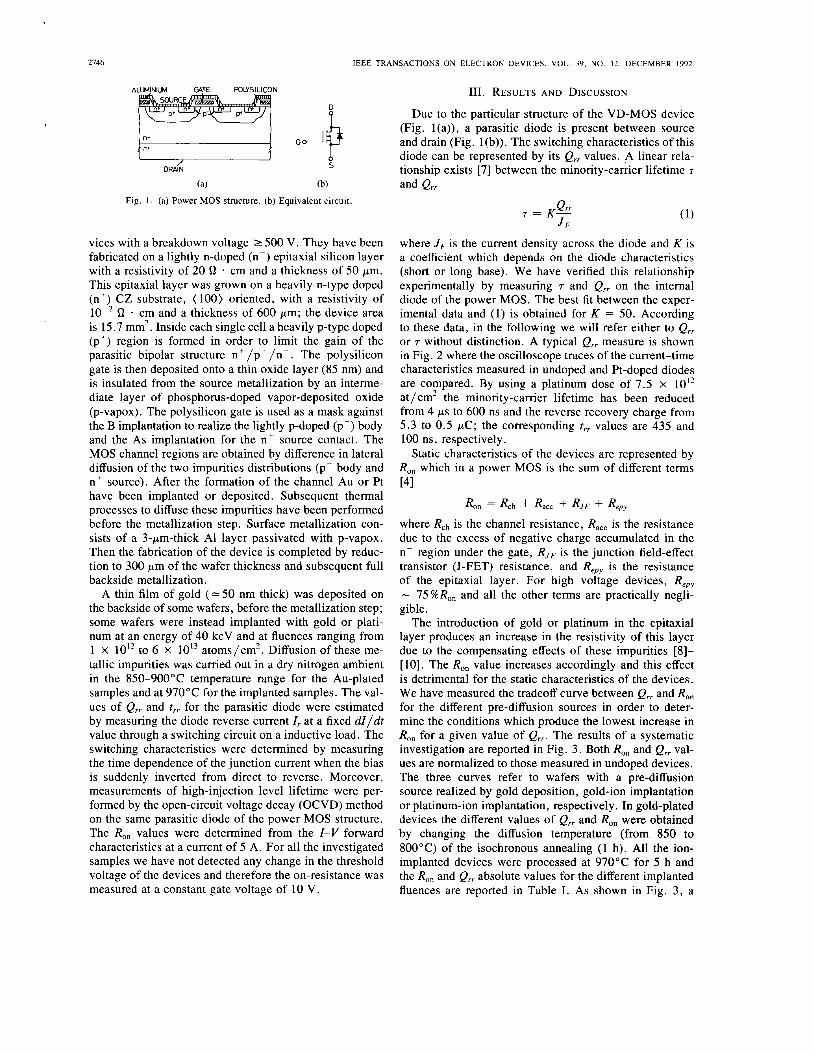
Fig. 1. (a) Power MOS structure. (b) Equivalent circuit.
vices with a breakdown voltage 1500 V. They have been fabricated on a lightly n-doped (n-) epitaxial silicon layer with a resistivity of 20 fl cm and a thickness of 50 pm. This epitaxial layer was grown on a heavily n-type doped (n+) CZ substrate, (100) oriented, with a resistivity of lo-' fl * cm and a thickness of 600 pm; the device area is 15.7 mm2. Inside each single cell a heavily p-type doped (p') region is formed in order to limit the gain of the parasitic bipolar structure n + /p' /n- . The polysilicon gate is then deposited onto a thin oxide layer (85 nm) and is insulated from the source metallization by an interme- diate layer of phosphorus-doped vapor-deposited oxide (p-vapox). The polysilicon gate is used as a mask against the B implantation to realize the lightly p-doped (p-) body and the As implantation for the n' source contact. The MOS channel regions are obtained by difference in lateral diffusion of the two impurities distributions (p- body and n+ source). After the formation of the channel Au or Pt have been implanted or deposited. Subsequent thermal processes to diffuse these impurities have been performed before the metallization step. Surface metallization con- sists of a 3-pm-thick A1 layer passivated with p-vapox. Then the fabrication of the device is completed by reduc- tion to 300 pm of the wafer thickness and subsequent full backside metallization.
A thin film of gold (= 50 nm thick) was deposited on the backside of some wafers, before the metallization step; some wafers were instead implanted with gold or plati- num at an energy of 40 keV and at fluences ranging from 1 X 10l2 to 6 X lOI3 atoms/cm'. Diffusion of these me- tallic impurities was carried out in a dry nitrogen ambient in the 850-900°C temperature range for the Au-plated samples and at 970°C for the implanted samples. The val- ues of Q,, and t,, for the parasitic diode were estimated by measuring the diode reverse current I , at a fixed dZ/dt value through a switching circuit on a inductive load. The switching characteristics were determined by measuring the time dependence of the junction current when the bias is suddenly inverted from direct to reverse. Moreover, measurements of high-injection level lifetime were per- formed by the open-circuit voltage decay (OCVD) method on the same parasitic diode of the power MOS structure. The Ron values were determined from the Z-I/ forward characteristics at a current of 5 A. For all the investigated samples we have not detected any change in the threshold voltage of the devices and therefore the on-resistance was measured at a constant gate voltage of 10 V.
111. RESULTS AND DISCUSSION
Due to the particular structure of the VD-MOS device (Fig. l(a)), a parasitic diode is present between source and drain (Fig. l(b)). The switching characteristics of this diode can be represented by its Q,, values. A linear rela- tionship exists [7] between the minority-carrier lifetime T and Qrr
(1)
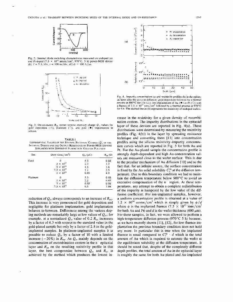
where JF is the current density across the diode and K is a coefficient which depends on the diode characteristics (short or long base). We have verified this relationship experimentally by measuring T and Q,, on the internal diode of the power MOS. The best fit between the exper- imental data and (1) is obtained for K = 50. According to these data, in the following we will refer either to Q,, or 7 without distinction. A typical Q,, measure is shown in Fig. 2 where the oscilloscope traces of the current-time characteristics measured in undoped and Pt-doped diodes are compared. By using a platinum dose of 7.5 x lo1* at /cm2 the minority-carrier lifetime has been reduced from 4 ps to 600 ns and the reverse recovery charge from 5.3 to 0.5 pC; the corresponding f,, values are 435 and 100 ns, respectively.
Static characteristics of the devices are represented by Ron which in a power MOS is the sum of different terms
Qrr T = K-
J F
[41
Ron = Rch Racc -k RJF -k Rep, where Rch is the channel resistance, Race is the resistance due to the excess of negative charge accumulated in the n- region under the gate, RjF is the junction field-effect transistor (J-FET) resistance, and Rep, is the resistance of the epitaxial layer. For high voltage devices, Rep, - 75%ROn and all the other terms are practically negli- gible.
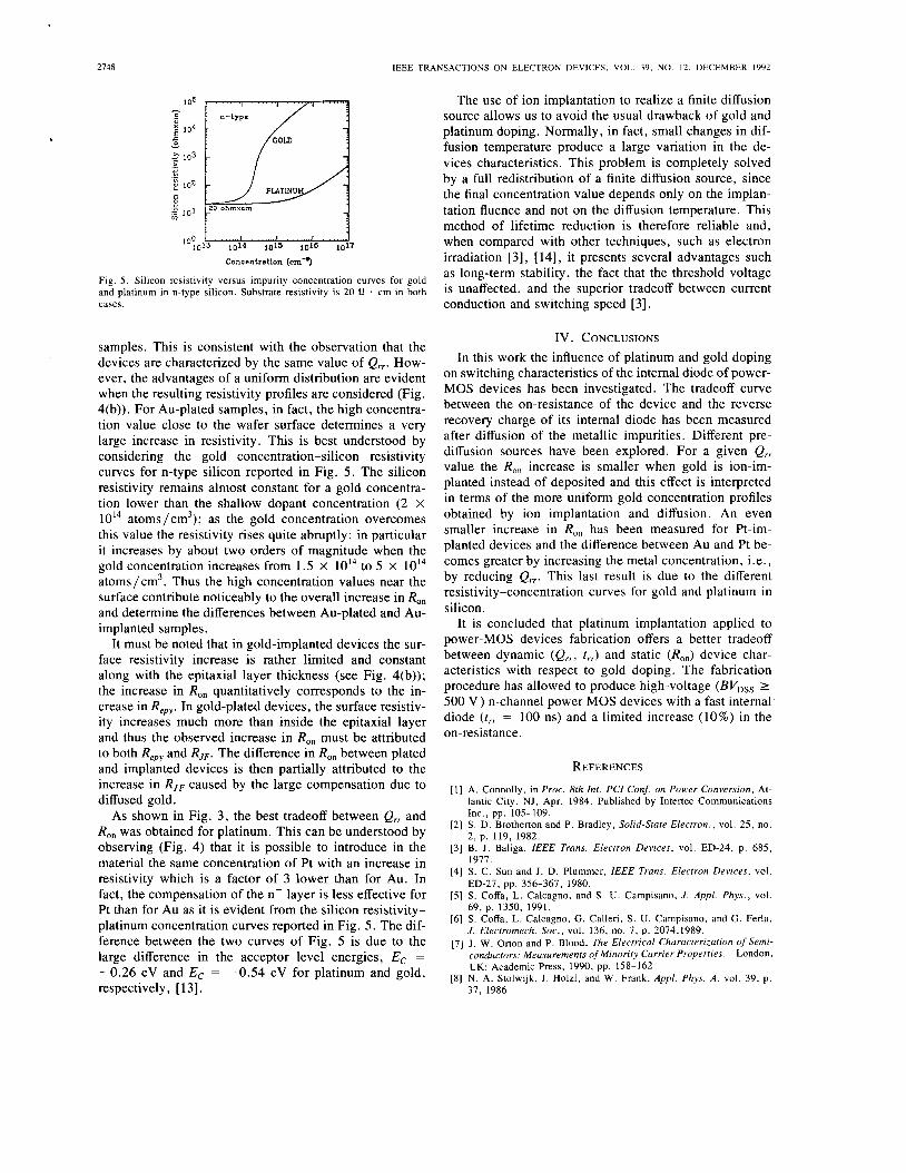
The introduction of gold or platinum in the epitaxial layer produces an increase in the resistivity of this layer due to the compensating effects of these impurities [8]- [ 101. The Ron value increases accordingly and this effect is detrimental for the static characteristics of the devices. We have measured the tradeoff curve between Q,, and Ron for the different pre-diffusion sources in order to deter- mine the conditions which produce the lowest increase in Ron for a given value of Qrr. The results of a systematic investigation are reported in Fig. 3 . Both Ron and Q,, val- ues are normalized to those measured in undoped devices. The three curves refer to wafers with a pre-diffusion source realized by gold deposition, gold-ion implantation or platinum-ion implantation, respectively. In gold-plated devices the different values of Q,, and Ron were obtained by changing the diffusion temperature (from 850 to 800°C) of the isochronous annealing (1 h). All the ion- implanted devices were processed at 970°C for 5 h and the Ron and Q,, absolute values for the different implanted fluences are reported in Table I. As shown in Fig. 3 , a
CATANIA er al.: TRADEOFF BETWEEN SWITCHING SPEED OF THE INTERNAL DIODE AND ON-RESISTANCE 2141
6 I I I I - - 0 Pt implontotion E 5: >
(a) 5 -8
I CO 4 - e Au implantation - E -10 v 8 Au deposition
- -
2 -20 2 2 - A -
c A A 8
0 500 1000 p 1- -8 8 8 A 8 8 8 t ime(ns) 0
O O I I I I
i o 3 - - * E A
ltiil Fig. 2. Internal diode switching characteristics measured on undoped (a) and Pt-doped (7.5 X IO'* atoms/cm*, 970°C, 5 h) power-MOS device (b). I = 5 A/div, t = 100 ns/div, d I / d t = 100 A / p .
3u
40 0 m .
D
N 30- - m 5 - z
2 0 -
-
-
4 00
o Pt implant . Au "(ant n Au deposition
o Pt implant . Au "(ant n Au deposition
/ , I / I I I I I 0 2 0 4 0 6 0 8 10
Normalized Qrr
Fig. 3. On-resistance R,, versus reverse recovery charge Q,, values for gold deposition ( A ) , platinum (O), and gold ( 0 ) implantation in silicon.
TABLE I EXPERIMENTAL VALUES OF THE REVERSE RECOVERY CHARGES e,, OF THE INTERNAL DIODES AND THE OUTPUT RESISTANCE OF POWER-MOS DEVICES
IMPLANTED WITH DIFFERENT FLUENCES OF GOLD OR PLATINUM
Gold 0 3 x 1Ol2 5 x l o k 2
7.5 x 1oI2 1 x IO i2
1 x I O 1 * 5 x IO'*
7.5 x IO'*
Platinum 0
5.3 2.3 1.5 1.1 0.85
5.3 2.2 0.95 0.5
0.88 1.2 I .6 2.5 4.0
0.88 0.95 0.98 1.08
reduction of Q,, always corresponds to an increase of Ron. This increase is very pronounced for gold deposition and negligible for platinum implantation; gold implantation behaves in-between. Differences among the various dop- ing methods are remarkably large at low values of Q,,; for example, at a normalized Q,, value of 0.2 Ron increases by a factor of 4.3 with respect to the standard value in the gold-plated sample but only by a factor of 2.8 in the gold- implanted samples. In platinum-implanted samples it is possible to reduce Q,, by a factor of 10 with a limited increase ( - 20%) in Ron. As Q,, mainly depends on the concentration of recombination centers in the n- epitaxial layer and Ron on the resulting resistivity profile in this layer, the best compromise between Q,, and Ron is achieved by the method which produces the lowest in-
(b) $ l o ' 1 I I I I I I 0 10 20 30 40 50
Depth ( r m )
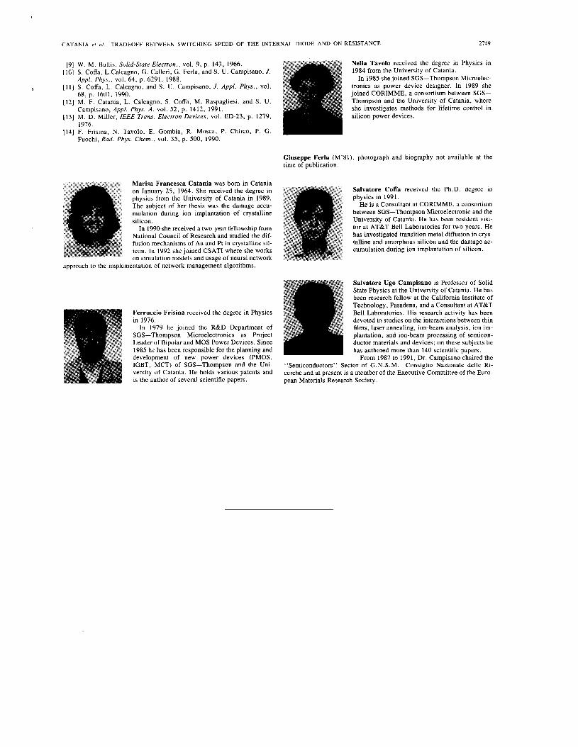
Fig. 4. Impurity concentration (a) and resistivity profiles (b) in the epitax- ial layer after the drive-in diffusion: gold deposition followed by a thermal process at 880°C for 1 h ( A ) ; ion implantation of Au ( 0 ) or Pt (0) with a fluence of 7.5 x I O i 2 ions/cm* followed by a thermal process at 970°C for 5 h. The dashed line in (b) represents the resistivity of undoped wafers.
crease in the resistivity for a given density of recombi- nation centers. The impurity distributions in the epitaxial layer of these devices are reported in Fig. 4(a). These distributions were determined by measuring the resistivity profiles (Fig. 4(b)) in the layer by spreading resistance technique and converting them [ 1 11 into concentration profiles using the silicon resistivity-impurity concentra- tion curves which are reported in Fig. 5 for both Au and Pt. For the Au-plated sample the concentration profile is strongly depth-dependent and high Au-concentration val- ues are measured close to the wafer surface. This is due to the peculiar mechanism of Au diffusion [ 101 and to the fact that, for an infinite source, the surface concentration is fixed by the Au solid solubility Czq at the diffusion tem- perature. Due to this boundary condition we had to main- tain the diffusion temperature below 900°C to avoid an excessive compensation of the n- region. At these tem- peratures, any attempt to obtain a complete redistribution of the impurity is hampered by the low value of the dif- fusion coefficient. For ion-implanted samples, however, a uniform concentration profile is obtained at a value of 1.2 x 10¹⁴ atoms/cm3 which is simply given by + / d where + is the implanted fluence (7.5 X lok2 ions/cm2 for both Au and Pt) and d is the wafer thickness (600 pm). For these samples, in fact, we were allowed to perform a high-temperature diffusion process (970°C 5 h) because, as we have recently shown [ 1 11, [ 121, for low-fluence im- plantation the previous boundary condition does not hold any more. In particular this is true when the implanted fluence is small compared to CSeq * d which is the total amount of Au which is required to saturate the wafer at the equilibrium solubility at the diffusion temperature. It should be noted that, despite of the completely different depth profiles, the total amount of Au in the epitaxial layer is roughly the same for both Au-plated and Au-implanted
2748 IEEE TRANSACTIONS ON ELECTRON DEVICES, VOL. 39, NO. 12. DECEMBER 1992
Fig. 5. Silicon resistivity versus impurity concentration curves for gold and platinum in n-type silicon. Substrate resistivity is 20 fl . cm in both cases.
samples. This is consistent with the observation that the devices are characterized by the same value of Q,,. How- ever, the advantages of a uniform distribution are evident when the resulting resistivity profiles are considered (Fig. 4(b)). For Au-plated samples, in fact, the high concentra- tion value close to the wafer surface determines a very large increase in resistivity. This is best understood by considering the gold concentration-silicon resistivity curves for n-type silicon reported in Fig. 5 . The silicon resistivity remains almost constant for a gold concentra- tion lower than the shallow dopant concentration (2 x 10¹⁴ atoms /cm3); as the gold concentration overcomes this value the resistivity rises quite abruptly: in particular it increases by about two orders of magnitude when the gold concentration increases from 1 . 5 X 10¹⁴ to 5 x 10¹⁴ atoms/cm3. Thus the high concentration values near the surface contribute noticeably to the overall increase in Ron and determine the differences between Au-plated and Au- implanted samples.
It must be noted that in gold-implanted devices the sur- face resistivity increase is rather limited and constant along with the epitaxial layer thickness (see Fig. 4(b)); the increase in Ron quantitatively corresponds to the in- crease in Repy. In gold-plated devices, the surface resistiv- ity increases much more than inside the epitaxial layer and thus the observed increase in Ron must be attributed to both Rep, and RjF. The difference in Ron between plated and implanted devices is then partially attributed to the increase in RjF caused by the large compensation due to diffused gold.
As shown in Fig. 3 , the best tradeoff between Q,, and Ron was obtained for platinum. This can be understood by observing (Fig. 4) that it is possible to introduce in the material the same concentration of Pt with an increase in resistivity which is a factor of 3 lower than for Au. In fact, the compensation of the n- layer is less effective for Pt than for Au as it is evident from the silicon resistivity- platinum concentration curves reported in Fig. 5 . The dif- ference between the two curves of Fig. 5 is due to the large difference in the acceptor level energies, Ec = -0.26 eV and Ec = - 0 . 5 4 eV for platinum and gold, respectively, [ 1 3 1 .
The use of ion implantation to realize a finite diffusion source allows us to avoid the usual drawback of gold and platinum doping. Normally, in fact, small changes in dif- fusion temperature produce a large variation in the de- vices characteristics. This problem is completely solved by a full redistribution of a finite diffusion source, since the final concentration value depends only on the implan- tation fluence and not on the diffusion temperature. This method of lifetime reduction is therefore reliable and, when compared with other techniques, such as electron irradiation [3], [ 141, it presents several advantages such as long-term stability, the fact that the threshold voltage is unaffected, and the superior tradeoff between current conduction and switching speed [ 3 ] .
IV. CONCLUSIONS In this work the influence of platinum and gold doping
on switching characteristics of the internal diode of power- MOS devices has been investigated. The tradeoff curve between the on-resistance of the device and the reverse recovery charge of its internal diode has been measured after diffusion of the metallic impurities. Different pre- diffusion sources have been explored. For a given Q,, value the Ron increase is smaller when gold is ion-im- planted instead of deposited and this effect is interpreted in terms of the more uniform gold concentration profiles obtained by ion implantation and diffusion. An even smaller increase in Ron has been measured for Pt-im- planted devices and the difference between Au and Pt be- comes greater by increasing the metal concentration, i.e., by reducing Q,,. This last result is due to the different resistivity-concentration curves for gold and platinum in silicon.
It is concluded that platinum implantation applied to power-MOS devices fabrication offers a better tradeoff between dynamic (Q,,, t,,) and static (Ron) device char- acteristics with respect to gold doping. The fabrication procedure has allowed to produce high-voltage (BVDSs 2 500 V ) n-channel power MOS devices with a fast internal- diode (r,, = 100 ns) and a limited increase (10%) in the on-resistance.
REFERENCES
[ I ] A. Connolly, in Proc. 8th Int. PCI Con5 on Power Conversion, At- lantic City, NJ, Apr. 1984. Published by Intertec Communications Inc., pp. 105-109.
[2] S . D. Brotherton and P. Bradley, Solid-Stare Electron., vol. 25, no. 2, p. 119, 1982.
[3] B. J . Baliga, IEEE Trans. Electron Devices, vol. ED-24, p. 685, 1977.
[4] S . C . Sun and J . D. Plummer, IEEE Trans. Electron Devices, vol.
[5] S . Coffa, L. Calcagno, and S . U. Campisano, J. Appl. Phys. , vol.
[6] S . Coffa, L. Calcagno, G . Calleri, S . U. Campisano, and G. Ferla,
[7] I. W. Orton and P. Blood, The Electrical Characterization of Semi- London,
[XI N . A . Stolwijk, J . Holzl, and W . Frank, Appl. Phys. A , vol. 39, p.
ED-27, pp. 356-367, 1980.
69, p. 1350, 1991.
J . Electromech. Soc. , vol. 136, no. 7, p. 2074,1989.
conductors: Measurements of Minority Carrier Properties. UK: Academic Press, 1990, pp. 158-162.
37, 1986.
CATANIA er al.: TRADEOFF BETWEEN SWITCHING SPEED OF THE INTERNAL DIODE AND ON-RESISTANCE 2149
W. M. Bullis, Solid-state Electron., vol. 9 , p. 143, 1966. S. Coffa, L.Calcagno, G. Calleri, G. Ferla, and S. U. Campisano, J . Appl. Phys., vol. 64, p. 6291, 1988. S. Coffa, L. Calcagno, and S. U. Campisano, J . Appl. Phys., vol. 68, p. 1601, 1990. M. F. Catania, L. Calcagno, S. Coffa, M. Raspagliesi, and S. U. Campisano, Appl. Phys. A , vol. 52, p. 1412, 1991. M. D. Miller, IEEE Trans. Electron Devices, vol. ED-23, p. 1279, 1976. F. Frisina, N. Tavolo, E. Gombia, R. Mosca, P. Chirco, P. G. Fuochi, Rad. Phys. Chem., vol. 35, p. 500, 1990.
Marisa Francesca Catania was born in Catania on January 25, 1964. She received the degree in physics from the University of Catania in 1989. The subject of her thesis was the damage accu- mulation during ion implantation of crystalline silicon.
In 1990 she received a two-year fellowship from National Council of Research and studied the dif- fusion mechanisms of Au and Pt in crystalline sil- icon. In 1992 she joined CSATI where she works on simulation models and usage of neural network -
approach to the implementation of network management algorithms.
Ferruccio Frisina received the degree in Physics in 1976.
In 1979 he joined the R&D Department of SGS-Thompson Microelectronics as Project Leader of Bipolar and MOS Power Devices. Since 1985 he has been responsible for the planning and development of new power devices (PMOS, IGBT, MCT) of SGS-Thompson and the Uni- versity of Catania. He holds various patents and is the author of several scientific papers.
Nella Tavolo received the degree in Physics in 1984 from the University of Catania.
In 1985 she joined SGS-Thompson Microelec- tronics as power device designer. In 1989 she joined CORIMME, a consortium between SGS- Thompson and the University of Catania, where she investigates methods for lifetime control in silicon power devices.
Giuseppe Ferla (M’Sl), photograph and biography not available at the time of publication.
Salvatore Coffa received the Ph.D. degree in physics in 199 1.
He is a Consultant at CORIMME, a consortium between SGS-Thompson Microelectronic and the University of Catania. He has been resident visi- tor at AT&T Bell Laboratories for two years. He has investigated transition metal diffusion in crys- talline and amorphous silicon and the damage ac- cumulation during ion implantation of silicon.
Salvatore Ugo Campisano is Professor of Solid State Physics at the University of Catania. He has been research fellow at the California Institute of Technology, Pasadena, and a Consultant at AT&T Bell Laboratories. His research activity has been devoted to studies on the interactions between thin films, laser annealing, ion-beam analysis, ion im- plantation, and ion-beam processing of semicon- ductor materials and devices; on these subjects he has authored more than 140 scientific papers.
From 1987 to 1991. Dr. Camuisano chaired the “Semiconductors” Sector of G.N.S.M.-Consiglio Nazionale delle Ri- cerche and at present is a member of the Executive Committee of the Euro- pean Materials Research Society.