optimization of processing and modeling issues for thin-film
TRANSCRIPT

November 1998 NREL/SR-520-25845
Optimization of Processing andModeling Issues for Thin-Film SolarCell Devices
Annual Report3 February 1997 - 2 February 1998
R.W. Birkmire, J.E. Phillips, W.N. Shafarman,S.S. Hegedus, and B.E. McCandlessInstitute of Energy ConversionUniversity of DelawareNewark, Delaware
National Renewable Energy Laboratory1617 Cole BoulevardGolden, Colorado 80401-3393A national laboratory of the U.S. Department of EnergyManaged by Midwest Research Institutefor the U.S. Department of Energyunder contract No. DE-AC36-83CH10093

NREL/SR-520-25845
Optimization of Processing andModeling Issues for Thin-Film SolarCell Devices
Annual Report3 February 1997 - 2 February 1998
R.W. Birkmire, J.E. Phillips, W.N. Shafarman,S.S. Hegedus, and B.E. McCandlessInstitute of Energy ConversionUniversity of DelawareNewark, Delaware
NREL technical monitor: B. von Roedern
National Renewable Energy Laboratory1617 Cole BoulevardGolden, Colorado 80401-3393A national laboratory of the U.S. Department of EnergyManaged by Midwest Research Institutefor the U.S. Department of Energyunder contract No. DE-AC36-83CH10093
Prepared under Subcontract No. XAK-7-17609-01
November 1998

NOTICE
This report was prepared as an account of work sponsored by an agency of the United Statesgovernment. Neither the United States government nor any agency thereof, nor any of their employees,makes any warranty, express or implied, or assumes any legal liability or responsibility for the accuracy,completeness, or usefulness of any information, apparatus, product, or process disclosed, or representsthat its use would not infringe privately owned rights. Reference herein to any specific commercialproduct, process, or service by trade name, trademark, manufacturer, or otherwise does not necessarilyconstitute or imply its endorsement, recommendation, or favoring by the United States government or anyagency thereof. The views and opinions of authors expressed herein do not necessarily state or reflectthose of the United States government or any agency thereof.
Available to DOE and DOE contractors from:Office of Scientific and Technical Information (OSTI)P.O. Box 62Oak Ridge, TN 37831
Prices available by calling 423-576-8401
Available to the public from:National Technical Information Service (NTIS)U.S. Department of Commerce5285 Port Royal RoadSpringfield, VA 22161703-605-6000 or 800-553-6847orDOE Information Bridgehttp://www.doe.gov/bridge/home.html
Printed on paper containing at least 50% wastepaper, including 10% postconsumer waste

i
SummaryThe overall mission of the Institute of Energy Conversion is the development of thin filmphotovoltaic cells, modules, and related manufacturing technology and the education of studentsand professionals in photovoltaic technology. The objectives of this four-year NREL subcontractare to advance the state of the art and the acceptance of thin film PV modules in the areas ofimproved technology for thin film deposition, device fabrication, and material and devicecharacterization and modeling, relating to solar cells based on CuInSe2 and its alloys, on a-Si andits alloys, and on CdTe.
CuInSe2-based Solar Cells
High Bandgap CuInSe2 Alloys
CuInSe2 has a bandgap of 1.0 eV and most Cu(InGa)Se2-based devices have absorber layers withGa/(In+Ga) ≈ 0.25 which gives a bandgap of 1.15 eV and results in devices with open circuitvoltages < 0.65V. Higher Ga concentrations to increase the Cu(InGa)Se2 bandgap result in atrade-off of higher open circuit voltage and lower short circuit current which may allow increasedcell efficiency. Further, module performance should be improved due to lower resistive losses,thinner ZnO with less optical loss and/or greater interconnect spacing with reduced associated area-related losses.
We have previously demonstrated Cu(InGa)Se2 solar cells with 15% efficiency for Ga/(In+Ga) ≤0.5 or bandgap (Eg) ≤ 1.3 eV [101, 102]. With higher bandgap a decrease in cell efficiency wasshown to be caused by poor collection of light generated minority carriers in the Cu(InGa)Se2absorber layers and in this report, we have expanded the characterization of Cu(InGa)Se2 deviceswith increasing Ga content and bandgap. Further, we have begun to investigate other CuInSe2-based alloy materials, CuInS2 and Cu(InAl)Se2, which may provide alternative means to achieveimproved device performance with Eg > 1.3 eV.
Reduced Cu(InGa)Se2 Deposition Temperature and Thickness
There are many technical issues which need to be addressed to effectively enable the transfer ofCu(InGa)Se2 deposition and device fabrication technology from the laboratory to manufacturingscale. In general, these issues provide a means to reduce thin film semiconductor process costs.Shorter deposition time can be achieved with reduced film thickness and increased deposition rate.Thinner absorber films reduce the total amount of material used and allow faster processthroughput. The minimum thickness of the Cu(InGa)Se2 absorber layer may be determined by thenucleation of the film to form a continuous layer or by the film morphology. From a deviceperspective, the minimum thickness may be determined by the minority carrier diffusion length andoptical absorption coefficient of the Cu(InGa)Se2 or the ability to incorporate optical confinement.
Lower substrate temperature (Tss) can lower processing costs by reducing thermally induced stresson the substrate, allowing faster heat-up and cool-down, and decreasing the heat load and stress onthe entire deposition system. In addition, with lower substrate temperature, stress on the glasssubstrate can be reduced and alternative substrate materials, like a flexible polymer web, could beutilized.
We have addressed the need to improve process throughput by reducing the Cu(InGa)Se2thickness and deposition temperature. The approach during this work has been to first define abaseline process for Cu(InGa)Se2 deposition by multisource elemental evaporation and solar cellfabrication. All other deposition parameters are then held fixed to determine the effects of varyingeither the substrate temperature or, by changing the deposition time, film thickness. Material

ii
properties of the resulting Cu(InGa)Se2 films have been characterized and their device behavior hasbeen measured and analyzed.
Team Participation
IEC is a member of the National CIS Team under the NREL Thin Film Partnership Program. TheCIS Team effort includes four working groups (WG). Of these, IEC has been a member of theTransient Effects WG and the New Junction WG, for which William Shafarman is the GroupLeader.
New Junction
The New Junction WG has identified two tasks and IEC has contributed to work on each. Theobjective of the first task is to develop non-cadmium containing buffer layers. The priority is onvacuum processes which could potentially be incorporated in-line, and chemical bath deposition isnot considered a primary option. The objective of the second task is to develop improved TCOlayers to minimize losses for module fabrication and quantify the effect of TCO layers on moduleperformance. This task is focusing on the high conductivity TCO layers.
Transient Effects
The CuInSe2 thin film partnership program organized a transient effects team to determine ifpresent I-V testing procedures can predict the daily output of CuInSe2-based modules and cellsunder field conditions; and, if they cannot, to determine what new testing procedures are needed.
a-Si:H-based Solar Cells
The focus of a-Si research was on contacts and interfaces. This work was motivated by resultsfrom the previous year which showed that the electrical behavior of the n-layer/TCO contact wascritical to incorporating a high performance TCO/Ag back reflector and achieving efficiencies over10%.
Current-Voltage Characterization of TCO Contacts
We investigated the current-voltage-temperature dependence of the following contacts, where TCOrefers to sputtered ITO or ZnO: TCO/a-Si i-layer, TCO/a-Si n-layer, TCO/µc-Si n-layer, texturedSnO2/a-Si n-layer and textured SnO2/µc-Si n-layer. Regarding the contact between sputtered TCOand a-Si i-layers, ITO has a larger barrier compared to ZnO. Thus, ITO makes a better junction,hence poorer Ohmic contact, with a-Si i-layers. Also, sputtering ZnO in Ar/O2 gives a higherbarrier and more blocking contact with a-Si compared to sputtering ZnO in Ar or Ar/H2. Thus, thebarrier between ZnO and a-Si depends on the ZnO sputtering conditions. It is not known if this isan interfacial or bulk effect. Regarding the contact between sputtered TCO and a-Si or µc-Si n-layers, it was found that the µc-Si n-layers have nearly-Ohmic behavior with ITO, ZnO or SnO2contacts at T > 25°C unlike a-Si n-layers. The µc-Si n-layers have lower contact resistance than a-Si n-layers. JV behavior at T > 25°C with the a-Si or µc-Si n-layers was nearly independent of thevarious sputtered TCO contacts. We found that the a-Si n/SnO2 contact is more blocking at T <25°C than is the µc-Si n/SnO2 contact. Thus, µc-Si n-layers are essential for good Ohmic contactsto TCO for either top or bottom contacts. Their high conductivity allows the decoupling of theelectrical requirements for the contact from the optical requirements, and allows the device toachieve full benefit of an optical back reflector or other transparent contact without any additionalelectrical losses.

iii
We also investigated the contact between the p-layer and various glass/TCO substrates forsuperstrate p-i-n cells as part of our on-going study of ZnO/p contacts and ZnO substrates incollaboration with R. Gordon at Harvard University. It was found that a new process for APCVDZnO yields much better device performance than previous APCVD ZnO material, and thatstraightforward changes to the deposition of the p-layer, such as increasing the B dopant flow cangive significant improvements in FF and Voc of ZnO/p-i-n devices.
Effect of Interface on Voc
In an effort to improve the stabilized Voc, we attempted to duplicate studies from Penn State, NRELand elsewhere by modifying the initially deposited i-layer to include either hydrogen dilution orgraded a-SiC. This resulted in only a small (~10 mV) improvement in initial Voc and noimprovement in degraded Voc or efficiency. We conclude that without hydrogen dilution of thebulk i-layer we will not see gains reported by others with hydrogen diluted interface layers sincethe bulk degradation dominates.
Team Participation
IEC is a member of the National a-Si Team under the Thin Film Partnership Program. SteveHegedus is the group leader of the Device Design and Interface team. Much of the work describedabove was performed as part of the teaming activities.
CdTe-based Solar Cells
Production of reliable and reproducible CdS window layers and contacts for stable, highperformance CdS/CdTe solar cells are the key issues confronting development of thin-film CdTesolar cells. Meeting these objectives with manufacturing-compatible processes is crucial tosatisfying the overall NREL program goals and requires an understanding of the controllingproperties and mechanisms. IEC research in this phase was concentrated on: 1) quantifying andcontrolling CdS-CdTe interaction; 2) analyzing CdTe contact formation and properties; and 3)analyzing device behavior after stress-induced degradation. Through extensive interaction with theNational CdTe R&D Team, the applicability of the results and processes to CdS/CdTe cells madeby different techniques has been demonstrated, enabling a consistent framework to be used forunderstanding the relationship between device fabrication and operation.
Devices With Thin CdS
IEC demonstrated improved understanding and control of CdS diffusion by employing evaporatedCdTe1-xSx absorber layers and by modifying post-deposition treatments to anneal crystal defectsprior to CdCl2 delivery. Significant results include: 1) determining the effect of CdTe1-xSx alloycomposition on the effective CdS diffusion rate; 2) reducing CdS window layer consumption by3X; 3) fabricating devices with Jsc > 25 mA/cm2 with evaporated CdS layers; 4) determining deviceperformance as a function of final CdS thickness; and 5) development of an all-vapor cellfabrication process.
Quantification of CdS-CdTe Interdiffusion
During Phase I, fundamental issues confronting fabrication of devices with ultra-thin CdS wereinvestigated, allowing the CdS consumption process to be understood and controlled. Throughteaming activity, the role of TCO properties was further elucidated. In particular: 1) measurementprotocols were developed to analyze pinholes in the CdS layer and CdS diffusion into the absorberlayer; 2) low-temperature equilibrium data points were added to the CdS-CdTe phase diagram; 3)CdS diffusion into CdTe-based absorber layers with a range of sulfur content was quantified; 4)

iv
CdS diffusion in CdTe was examined for varying post-deposition treatment conditions; 5) themicro-crystal structure of the resulting absorber and absorber-window layer interface wasexamined by TEM for varying post-deposition treatment conditions; 6) a complete materialsanalysis with respect to interdiffusion in CdTe/CdS cells was made using CdTe/CdS furnished bysix groups of the CdTe Team, leading to development of a phenomenological model of CdTe/CdSdevices; and 7) TCO properties were identified which render the device structure more tolerant tocomplete CdS loss, leading to improvements in baseline efficiency of physical vapor depositedCdTe/CdS devices.
Contact to CdTe
A key chemical component of working CdTe contacts was clearly identified for the “wet chemical”fabrication processes typically employed and an alternative, all-vapor, method for fabricating lowresistance contacts was developed. Measurement protocols using variations in light intensity andtemperature during current-voltage measurements were employed to analyze the CdTe contactcharacteristics of devices made by different processes having different contacts. Coupled with thestress-induced degradation and recontacting studies being carried jointly with the CdTe StabilityTeam, a model is being formulated which links operational and stability aspects of CdTe/CdS cells.
Team Participation
IEC actively participated in the National CdTe R&D Team by fabricating contacts for the stabilitysub-team and devices for the CdS sub-team, analyzing films and devices for both sub-teams,reporting results through presentations and written reports, and hosting a full-day team meeting onApril 30, 1997. In particular, devices were fabricated on different TCO to augment investigationof TCO/CdTe junction influence as d(CdS) is reduced. Contacts to CdTe were deposited andevaluated on CdTe/CdS samples from Solar Cells, Inc., using five different conductors, and fromGolden Photon, Inc. A comprehensive x-ray diffraction analysis was performed on samples madeby six groups within the team, and a full report was submitted at the April, 1997 team meeting.

v
LIST OF CONTRIBUTORS
PRINCIPAL INVESTIGATORSRobert W. BirkmireSteven S. HegedusBrian E. McCandlessJames E. PhillipsT.W.F. RussellWilliam N. Shafarman
PRINCIPAL RESEARCHERSWayne A. BuchananMarylin Huff
VISITING PROFESSIONALSErten Eser, Visiting ScientistDirk Hofmann, Visiting ScholarJosef Kallo, Visiting ScholarSylvain Marsillac, Visiting ScholarJulius Mwabora, Fulbright FellowNese Orbey, Visiting EngineerIssakha Youm, Fulbright ScholarXiangbo Zeng, Visiting Scholar
POST-DOCTORAL FELLOWSMichael MaldeiMatheswaran MarudachalamSandeep VermaRobert WunderJie Zhu
TECHNICAL SUPPORTCharles DeboRonald DozierShannon FieldsSally GordonDmitriy GusakovKevin HartTom Hughes-LamprosJohn LakerHerbert Wardell
GRADUATE STUDENTSDaniel AikenMichael EngelmannHao FengMoses HaimbodiGreg HanketWei LiuChao Ying Ni

vi
Atul PantDavid SmithJochen TitusZhao-Hui Yang
STUDENTSBrian AtkinsonGeorge BrownChris CampbellCarrie DesimoneDaniel EichenwaldKelly KuhnsNatalie PaolantonioJohnny Yu
DOCUMENT PREPARATIONLinda Granger
vii
TABLE OF CONTENTS
SUMMARY..................................................................................................i
LIST OF CONTRIBUTORS ......................................................................... v
TABLE OF CONTENTS............................................................................ vii
LIST OF FIGURES.................................................................................... ix
LIST OF TABLES.....................................................................................xiv
1. INTRODUCTION ....................................................................................1
1.1 CuInSe2-based Solar Cells . . . . . . . . . . . . . . . . . . . . . . . . . . . . . . . . . . . . . . . . . . . . . . . . . . . . . . 1
1 . 2 a - S i : H - b a s e d S o l a r C e l l s . . . . . . . . . . . . . . . . . . . . . . . . . . . . . . . . . . . . . . . . . . . . . . . . . . . . . . . . 1
1.3 CdTe-based Solar Cells . . . . . . . . . . . . . . . . . . . . . . . . . . . . . . . . . . . . . . . . . . . . . . . . . . . . . . . . . 2
1 . 4 O r g a n i z a t i o n o f t h e R e p o r t . . . . . . . . . . . . . . . . . . . . . . . . . . . . . . . . . . . . . . . . . . . . . . . . . . . . . . 2
2. CuInSe2-BASED SOLAR CELLS ...........................................................3
2.1 High Bandgap CuInSe2 A l l o y s . . . . . . . . . . . . . . . . . . . . . . . . . . . . . . . . . . . . . . . . . . . . . . . . . . 32.1.1 Introduction ... . . . . . . . . . . . . . . . . . . . . . . . . . . . . . . . . . . . . . . . . . . . . . . . . . . . . . . . . . . . . . . . . . . . . . . . . . . . . . . . . . . . .32.1.2 Cu(In,Ga)Se2 device analysis...................................................................32.1.3 CuInS2 . . . . . . . . . . . . . . . . . . . . . . . . . . . . . . . . . . . . . . . . . . . . . . . . . . . . . . . . . . . . . . . . . . . . . . . . . . . . . . . . . . . . . . . . . . . . .52.1.4 Cu(InAl)Se2 . . . . . . . . . . . . . . . . . . . . . . . . . . . . . . . . . . . . . . . . . . . . . . . . . . . . . . . . . . . . . . . . . . . . . . . . . . . . . . . . . . . . . . .8
2.2 Reduced Cu(InGa)Se2 Deposition Temperature and Thickness... . . . . . . . . . . .122.2.1 Introduction .. . . . . . . . . . . . . . . . . . . . . . . . . . . . . . . . . . . . . . . . . . . . . . . . . . . . . . . . . . . . . . . . . . . . . . . . . . . . . . . . . . . .122.2.2 Experimental procedures.......................................................................122.2.3 Results: Deposition temperature .. . . . . . . . . . . . . . . . . . . . . . . . . . . . . . . . . . . . . . . . . . . . . . . . . . . . . . . . . . . . .132.2.4 Results: Film thickness .. . . . . . . . . . . . . . . . . . . . . . . . . . . . . . . . . . . . . . . . . . . . . . . . . . . . . . . . . . . . . . . . . . . . . . .162.2.5 Device measurements and analysis...........................................................16
2.3 Teaming Results . . . . . . . . . . . . . . . . . . . . . . . . . . . . . . . . . . . . . . . . . . . . . . . . . . . . . . . . . . . . . . . . 1 82.3.1 Introduction .. . . . . . . . . . . . . . . . . . . . . . . . . . . . . . . . . . . . . . . . . . . . . . . . . . . . . . . . . . . . . . . . . . . . . . . . . . . . . . . . . . . .182.3.2 New junction results . . . . . . . . . . . . . . . . . . . . . . . . . . . . . . . . . . . . . . . . . . . . . . . . . . . . . . . . . . . . . . . . . . . . . . . . . . .182.3.3 Transient Effects................................................................................21
3. a-Si:H-BASED SOLAR CELLS............................................................40
3 . 1 S u m m a r y . . . . . . . . . . . . . . . . . . . . . . . . . . . . . . . . . . . . . . . . . . . . . . . . . . . . . . . . . . . . . . . . . . . . . . . . . 4 0
3.2 PECVD system operat ional improvements . . . . . . . . . . . . . . . . . . . . . . . . . . . . . . . . . . . .40

viii
3.3 Device deposition conditions . . . . . . . . . . . . . . . . . . . . . . . . . . . . . . . . . . . . . . . . . . . . . . . . . . 4 1
3.4 Devices with continuous plasma “soft start” p-layer.. . . . . . . . . . . . . . . . . . . . . . . .42
3.5 Effect of interface layers on Voc a n d s t a b i l i t y . . . . . . . . . . . . . . . . . . . . . . . . . . . . . . . . . 4 3
3.6 Effect of p-layer doping and alternate TCO substrates: ZnO andSnO2/ Z n O . . . . . . . . . . . . . . . . . . . . . . . . . . . . . . . . . . . . . . . . . . . . . . . . . . . . . . . . . . . . . . . . . . . . . . . . 4 5
3.7 Electrical and optical study of high performance TCO/metalback reflector . . . . . . . . . . . . . . . . . . . . . . . . . . . . . . . . . . . . . . . . . . . . . . . . . . . . . . . . . . . . . . . . . . . 4 7
3.8 Electrical characterization of sputtered TCO junctions on a-Sia n d µ c - S i n a n d i - l a y e r s . . . . . . . . . . . . . . . . . . . . . . . . . . . . . . . . . . . . . . . . . . . . . . . . . . . . . . . . 4 7
4. CdTe-BASED SOLAR CELLS..............................................................58
4 . 1 S u m m a r y . . . . . . . . . . . . . . . . . . . . . . . . . . . . . . . . . . . . . . . . . . . . . . . . . . . . . . . . . . . . . . . . . . . . . . . . . 5 84.1.1 Devices with Thin CdS ... . . . . . . . . . . . . . . . . . . . . . . . . . . . . . . . . . . . . . . . . . . . . . . . . . . . . . . . . . . . . . . . . . . . . .584.1.2 Quantification of CdS-CdTe Interdiffusion..................................................584.1.3 Contact to CdTe.................................................................................584.1.4 Team Participation..............................................................................59
4 . 2 B a c k g r o u n d . . . . . . . . . . . . . . . . . . . . . . . . . . . . . . . . . . . . . . . . . . . . . . . . . . . . . . . . . . . . . . . . . . . . . . 5 94.2.1 Framework Relating CdTe/CdS Fabrication Technologies................................594.2.2 Critical issues .. . . . . . . . . . . . . . . . . . . . . . . . . . . . . . . . . . . . . . . . . . . . . . . . . . . . . . . . . . . . . . . . . . . . . . . . . . . . . . . . . .66
4.3 CdS-CdTe Interaction . . . . . . . . . . . . . . . . . . . . . . . . . . . . . . . . . . . . . . . . . . . . . . . . . . . . . . . . . . 6 64.3.1 Approach and Techniques.....................................................................664.3.2 CdS Window-Absorber Layer Interaction...................................................794.3.3 Devices with CdTe1-xSx Absorber Layers and Modified Post-Deposition Treatment...914.3.4 Influence of TCO..............................................................................102
4.4 CdTe Contacting in Device Structures . . . . . . . . . . . . . . . . . . . . . . . . . . . . . . . . . . . . . . 1034.4.1 Introduction ... . . . . . . . . . . . . . . . . . . . . . . . . . . . . . . . . . . . . . . . . . . . . . . . . . . . . . . . . . . . . . . . . . . . . . . . . . . . . . . . . .1034.4.2 Physio-chemical Analysis of Contact Operation...........................................1044.4.3 Electronic Analysis of Contact Operation...................................................1064.4.4 Stress Testing and Analysis..................................................................1074.4.5 Operational Model.............................................................................111
5. ABSTRACT........................................................................................112
6. REFERENCES...................................................................................113
ix
LIST OF FIGURES
Figure 2.1 Schematic diagram of the H2Se/H2S CVD reactor including gashandling and waste treatment. . . . . . . . . . . . . . . . . . . . . . . . . . . . . . . . . . . . . . . . . . . . . . . . . . . . . 7
Figure 2.2 XRD scans of In films on 7059 (top) and soda lime (bottom)substrates after they were reacted in H2S at 550°C for 90 min. . . . . . . . . . . . . . . . . 7
Figure 2.3 SEM micrographs at 2000x magnification showing the changein morphology of Cu/In films reacted at different H2S concentrations. . . . . . . . 8
Figure 2.4 XRD pattern of a film obtained by selenizing Al/In/Cu precursorat 550°C. The Al/(Al+In) ratio in the precursor is ≈ 0 .45 .CIS = CuInSe2, CIAS = CuIn1-xAlxSe2. . . . . . . . . . . . . . . . . . . . . . . . . . . . . . . . . . . . . . . . . . . 1 0
Figure 2.5 XRD plots of various peaks of a CuIn1-xAlxSe2 films(from run L0393). The Al/Al+In) concentrations in the legendsare intended ratios in the precursors. . . . . . . . . . . . . . . . . . . . . . . . . . . . . . . . . . . . . . . . . . . . 1 1
Figure 2.6 Deposition profile showing source and substrate temperaturesfor a standard run with Tss = 450°C. . . . . . . . . . . . . . . . . . . . . . . . . . . . . . . . . . . . . . . . . . . . . 1 3
Figure 2.7 SEM micrographs showing a decrease in grain size asTss d e c r e a s e s f r o m 6 0 0 t o 4 0 0 ° C . . . . . . . . . . . . . . . . . . . . . . . . . . . . . . . . . . . . . . . . . . . . . . . . . 1 4
Figure 2.8 SIMS depth profiles of Cu, In, Ga, Se, Mo, and Na forfilms deposited with (a) Tss = 600°C, (b) 500°C, and (c) 400°C. . . . . . . . . . . . . .15
Figure 2.9 Jsc, V oc, FF and efficiency vs. recovery time for deviceIEC-32702-32-7 after stress at a temperature of 80°C, in the darka n d 0 V f o r 1 2 h o u r s . . . . . . . . . . . . . . . . . . . . . . . . . . . . . . . . . . . . . . . . . . . . . . . . . . . . . . . . . . . . . . 2 2
Figure 2.10 Jsc, V oc, FF and efficiency vs. recovery time for deviceIEC-32702-32-7 after stress at a temperature of 80°C, in the darkand at a forward current of 30 mA/cm2 f o r 1 0 h o u r s . . . . . . . . . . . . . . . . . . . . . . . . . . . 2 3
Figure 2.11 Jsc, V oc, FF and efficiency vs. recovery time for deviceIEC-32702-32-7 after stress at a temperature of 80°C, in the darkand at V = -0.5 V for 12 hours. . . . . . . . . . . . . . . . . . . . . . . . . . . . . . . . . . . . . . . . . . . . . . . . . . 2 4
Figure 2.12 Jsc, V oc, FF and efficiency vs. recovery time for deviceIEC-32702-32-7 after stress at a temperature of 80°C, AM1 illuminationand at a forward current of mA/cm2 for 12 hours. . . . . . . . . . . . . . . . . . . . . . . . . . . . . . 2 5
Figure 2.13 Jsc, V oc, FF and efficiency vs. recovery time for deviceIEC-32702-32-7 after stress at a temperature of 80°C, AM1 illuminationand at V = -0.5 V for 12 hours. . . . . . . . . . . . . . . . . . . . . . . . . . . . . . . . . . . . . . . . . . . . . . . . . . 2 6
Figure 2.14 Jsc, V oc, FF and efficiency vs. recovery time for deviceIEC-32702-32-7 after stress at a temperature of 80°C, AM1 illuminationand RL = 12.6 Ω-cm 2 f o r 1 0 h o u r s . . . . . . . . . . . . . . . . . . . . . . . . . . . . . . . . . . . . . . . . . . . . . . . 2 7
Figure 2.15 Jsc, V oc, FF and efficiency vs. recovery time for deviceIEC-32702-32-7 after stress at a temperature of 80°C, AM1 illuminationand at Voc f o r 8 . 5 h o u r s . . . . . . . . . . . . . . . . . . . . . . . . . . . . . . . . . . . . . . . . . . . . . . . . . . . . . . . . . . . 2 8
Figure 2.16 Jsc, V oc, FF and efficiency vs. recovery time for deviceIEC-32702-32-7 after stress at a temperature of 80°C, AM1 illuminationand at Jsc for 11 hours. . . . . . . . . . . . . . . . . . . . . . . . . . . . . . . . . . . . . . . . . . . . . . . . . . . . . . . . . . . . 2 9

x
Figure 2.17 Picture of a Siemens Solar Industries substrate with twoCuInSe2-based solar cells (area ~ 1.0 cm2) . . . . . . . . . . . . . . . . . . . . . . . . . . . . . . . . . . . . . 3 0
Figure 2.18 Efficiency, Voc, J sc and fill factor recovery under illuminationat 25°C of device SSI-255-F2 after being subject to a lamination cycle( s e e t e x t ) . . . . . . . . . . . . . . . . . . . . . . . . . . . . . . . . . . . . . . . . . . . . . . . . . . . . . . . . . . . . . . . . . . . . . . . . . . . 3 1
Figure 2.19 A plot of the slope of the J-V curve at various times duringrecovery (see text). . . . . . . . . . . . . . . . . . . . . . . . . . . . . . . . . . . . . . . . . . . . . . . . . . . . . . . . . . . . . . . . 3 2
Figure 2.20 Series resistance recovery under illumination (see text)............32Figure 2.21 Series resistance recovery in the dark (except for J-V testing). . . . 3 3Figure 2.22 Series resistance recovery with "blue" light (except for
J - V t e s t i n g ) . . . . . . . . . . . . . . . . . . . . . . . . . . . . . . . . . . . . . . . . . . . . . . . . . . . . . . . . . . . . . . . . . . . . . . . . 3 3Figure 2.23 Series resistance recovery with "red" light (except for
J - V t e s t i n g ) . . . . . . . . . . . . . . . . . . . . . . . . . . . . . . . . . . . . . . . . . . . . . . . . . . . . . . . . . . . . . . . . . . . . . . . . 3 4Figure 2.24 Transmission characteristics of the filters used to produce
"blue" and "red" illumination. . . . . . . . . . . . . . . . . . . . . . . . . . . . . . . . . . . . . . . . . . . . . . . . . . . . 3 4Figure 2.25 Voc, J sc and FF recovery under illumination at 30°C of
mini-module SSI-260-98 after being subject to a lamination cycle. . . . . . . . . . . 3 5Figure 2.26 dV/dJ behavior of mini-module SSI-260-98 before and after
lamination and after recovery at full illumination. . . . . . . . . . . . . . . . . . . . . . . . . . . . . . 3 6Figure 2.27 dV/dJ behavior of mini-module SSI-260-98 before and after
lamination and after recovery at 50% illumination. . . . . . . . . . . . . . . . . . . . . . . . . . . . . 3 6Figure 2.28 dV/dJ behavior of mini-module SSI-260-98 before and after
lamination and after recovery at 10% illumination. . . . . . . . . . . . . . . . . . . . . . . . . . . . . 3 7Figure 2.29 dV/dJ behavior of mini-module SSI-260-98 before and after
lamination and after recovery in the dark. . . . . . . . . . . . . . . . . . . . . . . . . . . . . . . . . . . . . . . 3 7Figure 2.30 R s recovery in the dark at 30°C of mini-module SSI-260-108
after being subject to a lamination cycle. . . . . . . . . . . . . . . . . . . . . . . . . . . . . . . . . . . . . . . . 3 8Figure 2.31 R s recovery in "red" light at 30°C of mini-module SSI-260-105
after being subject to a lamination cycle. . . . . . . . . . . . . . . . . . . . . . . . . . . . . . . . . . . . . . . . 3 8Figure 2.32 Transmission characteristics of the "red" filter used for the
illumination of mini-module SSI-260-105. . . . . . . . . . . . . . . . . . . . . . . . . . . . . . . . . . . . . . 3 9Figure 3.1 Voltage dependent QE ratio for devices with and without
soft start p-layers. Xc is ratio of QE/(0v)/(+0.5V) at 700 nm to thatat 450 nm. Run numbers refer to Table 3 .2 . . . . . . . . . . . . . . . . . . . . . . . . . . . . . . . . . . . .43
Figure 3.2 Stability of four devices with different i1 layers during200 hour light exposure. Note that there was no difference indegradation and that no stabilization occurs within 200 hours.The i2 l ayer was not hydrogen d i lu ted . . . . . . . . . . . . . . . . . . . . . . . . . . . . . . . . . . . . . . . . . . . 45
Figure 3.3 FF and Voc for devices on SnO2 (textured, Asahi) and ZnO(smooth, Harvard) for different B2H6 f lows in the a-SiC p-layer. . . . . . . . . . . . .47
Figure 3.4 Four device structures (depositions 4685-4688) used to studysputtered TCO and SnO2 contacts with a-Si and µc-Si i-layers and n-layers.48
Figure 3.5 Illuminated JV curves at 100, 25, and -60°C forglass/SnO2/n-i /TCO devices with a-Si n-layer (4688-11). . . . . . . . . . . . . . . . . . . . . .49

xi
Figure 3.6 Illuminated JV curves at 100, 25, and -60°C forglass/SnO2/n-i/TCO devices with µc-Si n-layer (4687-11). . . . . . . . . . . . . . . . . . . . 4 9
Figure 3.7 Illuminated JV curves at 25°C for glass/SnO2/n-i/TCOdevices with µc-Si n-layers and four different sputtered TCO contacts......50
Figure 3.8 Temperature dependence of Voc for four devices from Figure 3.7w i t h µ c - S i n - l a y e r . . . . . . . . . . . . . . . . . . . . . . . . . . . . . . . . . . . . . . . . . . . . . . . . . . . . . . . . . . . . . . . . . 5 1
Figure 3.9 Temperature dependence of Jo for four devices from Figure 3.8w i t h µ c - S i n - l a y e r . . . . . . . . . . . . . . . . . . . . . . . . . . . . . . . . . . . . . . . . . . . . . . . . . . . . . . . . . . . . . . . . . 5 2
Figure 3.10 Temperature dependence of series resistance Rs fromlight JV of devices from 4687 (glass/SnO2/µc-Si n/i/TCO). Lines aredrawn to guide the eye. Activation energy for 1/T > 0.0036 K -1 isa p p r o x i m a t e l y 0 . 0 8 e V . . . . . . . . . . . . . . . . . . . . . . . . . . . . . . . . . . . . . . . . . . . . . . . . . . . . . . . . . . . . 5 3
Figure 3.11 JV curves at 100, 25, and -60°C for device with µc-Si n-layer(4685-11) and sputtered ZnO (Ar) contact. Device structure isglass/SnO2/µc-Si n/ZnO. . . . . . . . . . . . . . . . . . . . . . . . . . . . . . . . . . . . . . . . . . . . . . . . . . . . . . . . . . 5 4
Figure 3.12 JV curves at 100, 25, and -60°C for device with a-Si n-layer(4686-11) and sputtered ZnO (Ar) contact. Device structure isglass/SnO2/ a - S i n / Z n O . . . . . . . . . . . . . . . . . . . . . . . . . . . . . . . . . . . . . . . . . . . . . . . . . . . . . . . . . . . . 5 4
Figure 3.13 JV curves at -60°C for devices with c-Si n-layer(4685 pieces) and sputtered TCO contacts . . . . . . . . . . . . . . . . . . . . . . . . . . . . . . . . . . . . . .57
Figure 3.14 JV curves at -60°C for devices with a-Si n-layer(4686 pieces) and sputtered TCO contacts . . . . . . . . . . . . . . . . . . . . . . . . . . . . . . . . . . . . . .57
Figure 4.1 Schematic cross-sectional views of as-deposited (left)and CdCl2- t r e a t e d C d T e / C d S c e l l s . . . . . . . . . . . . . . . . . . . . . . . . . . . . . . . . . . . . . . . . . . . . . . . 6 4
Figure 4.2 Schematic detail of the junction region in a CdTe/CdS device.......64Figure 4.3 Schematic cross-section view of physical deposition system for
CdTe1-xS x a b s o r b e r l a y e r s . . . . . . . . . . . . . . . . . . . . . . . . . . . . . . . . . . . . . . . . . . . . . . . . . . . . . . . . . 6 8Figure 4.4 Measured optical transmission, normalized for reflection
of CdS/ITO/7059 (samples from depositions 12148, 12157, 12176,a n d 1 2 1 4 3 ) . . . . . . . . . . . . . . . . . . . . . . . . . . . . . . . . . . . . . . . . . . . . . . . . . . . . . . . . . . . . . . . . . . . . . . . . . 6 9
Figure 4.5 Voc-limiting defects attributable to CdS and TCO processing........69Figure 4.6 Equivalent circuit and equation for parallel diodes between
CdTe/CdS and CdTe/TCO. . . . . . . . . . . . . . . . . . . . . . . . . . . . . . . . . . . . . . . . . . . . . . . . . . . . . . . . 7 0Figure 4.7 Optical arrangement used to survey CdS films.. . . . . . . . . . . . . . . . . . . . . . .71Figure 4.8 Optical transmission of CdS film and Corion 400 nm
b a n d p a s s f i l t e r . . . . . . . . . . . . . . . . . . . . . . . . . . . . . . . . . . . . . . . . . . . . . . . . . . . . . . . . . . . . . . . . . . . . . 7 1Figure 4.9 Optical micrographs of pinholes in PVD CdS film 120 nm thick....72Figure 4.10 Short wavelength quantum efficiency of CdTe/CdS thin-film
device (solid line) compared to CdS transmission (dotted line) afterremoval of Te-rich layers (sample 40992.31/12127.31). . . . . . . . . . . . . . . . . . . . . . .74
Figure 4.11 Data Example 1 - Broad scan and peak table - SCI 005 afterthinning to 2 µm. . . . . . . . . . . . . . . . . . . . . . . . . . . . . . . . . . . . . . . . . . . . . . . . . . . . . . . . . . . . . . . . . . 7 7
Figure 4.12 Data Example 2 - NRST reduction of CdTe1-xS x peaksof Example 1. . . . . . . . . . . . . . . . . . . . . . . . . . . . . . . . . . . . . . . . . . . . . . . . . . . . . . . . . . . . . . . . . . . . . . 7 8

xii
Figure 4.13 Equilibrium phase diagram for CdTe-CdS incorporatingIEC data for films and powder and film data fromR e f e r e n c e s 1 6 3 , 1 6 4 , 1 6 5 . . . . . . . . . . . . . . . . . . . . . . . . . . . . . . . . . . . . . . . . . . . . . . . . . . . . . . . . 7 9
Figure 4.14 Equivalent CdS thickness versus molar fraction of CdS inCdTe1-xS x for different total alloy film thicknesses. Single crystaldensit ies were assumed in this approximation. . . . . . . . . . . . . . . . . . . . . . . . . . . . . . . . . .80
Figure 4.15 X-ray diffraction line profile of CdTe1-xS x (511) after deviceprocessing (left) and optical transmission of CdS before processing anddev ice quantum e f f i c i ency (r ight ) . . . . . . . . . . . . . . . . . . . . . . . . . . . . . . . . . . . . . . . . . . . . . . . . 80
Figure 4.16 Narrow angle XRD peaks of different (hkl) forIEC sample 913 .12 af ter th inning to 2 µm. . . . . . . . . . . . . . . . . . . . . . . . . . . . . . . . . . . . . .83
Figure 4.17 Narrow angle (511) (top) and (440) (bottom) XRD peak profilesfor CSM samples with different CdS thickness. . . . . . . . . . . . . . . . . . . . . . . . . . . . . . . . 8 4
Figure 4.18 Narrow angle (511) XRD peak profiles for IEC samples withdifferent CdS thickness after thinning the CdTe layer to ~2 µm..............85
Figure 4.19 Narrow angle (511) XRD peak profiles for NREL samples withdifferent CdS thickness after thinning the CdTe layer to ~2 µm..............85
Figure 4.20 Narrow angle (511) XRD peak profiles for SCI samples withdifferent CdS thickness after thinning the CdTe layer to ~2 µm..............86
Figure 4.21 Narrow angle (511) XRD peak profiles for USF samples withdifferent CdS thickness after thinning the CdTe layer to ~2 µm..............86
Figure 4.22 Narrow angle (511) XRD peak profiles for UT samples withd i f f e r e n t C d S t h i c k n e s s . . . . . . . . . . . . . . . . . . . . . . . . . . . . . . . . . . . . . . . . . . . . . . . . . . . . . . . . . . . 8 7
Figure 4.23 Change in CdS thickness derived from optical methodscompared to that derived from X-ray diffraction measurements. . . . . . . . . . . . . . 8 8
Figure 4.24 Total thickness profile of CdTe/CdS on quartz thinnedwith 0.05% Br2-Ch3O H . . . . . . . . . . . . . . . . . . . . . . . . . . . . . . . . . . . . . . . . . . . . . . . . . . . . . . . . . . . 9 0
Figure 4.25 Glancing incidence XRD of CdS (004) on CdCl2-treatedCdTe/CdS/Quartz with CdTe thinned to profile shown in Figure 4.24;4° incidence Cu-kα. . . . . . . . . . . . . . . . . . . . . . . . . . . . . . . . . . . . . . . . . . . . . . . . . . . . . . . . . . . . . . . . 9 0
Figure 4.26 Molar fraction, x, of CdS in CdTe1-xS x films versus effusionrate ratio of CdS and CdTe evaporation sources. Molar fractiondetermined by EDS measurement of central piece in substrate array. . . . . . . . . 9 2
Figure 4.27 Absorption coefficient squared versus energy for selectedCdTe1-xS x films on CdS/ITO window layers over the range ofas -depos i ted compos i t ion ind icated . . . . . . . . . . . . . . . . . . . . . . . . . . . . . . . . . . . . . . . . . . . . . . 93
Figure 4.28 Absorption edge energy versus molar fraction, x, ofCdS in CdTe1-xS x for alloy layers on CdS/ITO. The solid linerepresents the funct ion in Equat ion 4 .8 . . . . . . . . . . . . . . . . . . . . . . . . . . . . . . . . . . . . . . . . .93
Figure 4.29 XRD spectra of single phase as-deposited CdTe0.91S 0.09 andthe same sample after heat treatment with CdCl2 a t 420°C in a ir . . . . . . . . . . . . . .94
Figure 4.30 XRD (511) line profile of 2.5 µm CdTe/0.2 µm CdS (dotted)and 2.5 µm CdTe0.95S 0.05/0.2 µm CdS (solid) after CdCl2 treatment withhigh CdCl2 c o n c e n t r a t i o n . . . . . . . . . . . . . . . . . . . . . . . . . . . . . . . . . . . . . . . . . . . . . . . . . . . . . . . . . 9 5

xiii
Figure 4.31 X-ray diffraction line profiles for CdTe1-xS x after chlorideprocessing at 420°C for 30 minutes in air. Top = CdCl2:MeOH;Middle = CdCl2 vapor; Bottom = HTA + CdCl2 vapor. . . . . . . . . . . . . . . . . . . . . . . . . 9 6
Figure 4.32 Voc versus CdS thickness for different alloy absorber layerconfigurations. Filled markers are for devices on ITO/7059. Opencircles are for devices with bi-layer SnO2 superstrates, to be discussedi n t h e n e x t s e c t i o n . . . . . . . . . . . . . . . . . . . . . . . . . . . . . . . . . . . . . . . . . . . . . . . . . . . . . . . . . . . . . . . . . 9 8
Figure 4.33 Jsc versus final CdS thickness in the devices of Figure 4.32.... . . .98Figure 4.34 SEM photographs of CdCl2 treated CdTe/CdS – no anneal (top)
and HTA (bottom) prior to CdCl2 t r e a t m e n t . . . . . . . . . . . . . . . . . . . . . . . . . . . . . . . . . . . . . 9 9Figure 4.35 XRD (511) line profile of 2.5 µm CdTe/0.2 µm CdS after
CdCl2 vapor treatment (dotted) and after anneal in argon at 580°C for10 minutes followed by CdCl2 t rea tment ( so l id ) . . . . . . . . . . . . . . . . . . . . . . . . . . . . . . 100
Figure 4.36 Cross-sectional TEM images of CdTe-CdS interface regionon CdCl2-treated samples with anneal (left) and without anneal (right)pr ior to ch lor ide t rea tment . . . . . . . . . . . . . . . . . . . . . . . . . . . . . . . . . . . . . . . . . . . . . . . . . . . . . . 100
Figure 4.37 Glancing incidence (4°) x-ray diffraction pattern of CdTedevice through thin chromium metal contact showing Cu2Te phase . . . . . . . . . 105
Figure 4.38 Voc vs T for device #40929-21-5 at AM1.5G. . . . . . . . . . . . . . . . . . . . . . 106Figure 4.39 Series resistance versus 1/T for the same device shown in
F i g u r e 4 . 3 8 . . . . . . . . . . . . . . . . . . . . . . . . . . . . . . . . . . . . . . . . . . . . . . . . . . . . . . . . . . . . . . . . . . . . . . 107Figure 4.40 J-V behavior of SCI cell with IEC carbon contact
before stressing. . . . . . . . . . . . . . . . . . . . . . . . . . . . . . . . . . . . . . . . . . . . . . . . . . . . . . . . . . . . . . . . . 107Figure 4.41 J-V behavior of same cell after stress at 100°C, 2 suns,
6 weeks @ Voc. . . . . . . . . . . . . . . . . . . . . . . . . . . . . . . . . . . . . . . . . . . . . . . . . . . . . . . . . . . . . . . . . . . 108Figure 4.42 Summarized J-V behavior of device # SSI 20632D3-3-1..... . . . . 109Figure 4.43 Dark J-V data and equivalent circuit fit for before degradation.. 109Figure 4.44 Summarized dark J-V data and equivalent circuit diode
parameters. . . . . . . . . . . . . . . . . . . . . . . . . . . . . . . . . . . . . . . . . . . . . . . . . . . . . . . . . . . . . . . . . . . . . . . 110Figure 4.45 Summarized dJ/dV behavior of device # SSI 20632D3-3-1. . . . . . 111

xiv
LIST OF TABLES
Table 2.1 J-V parameters for various Cu(In,Ga)Se2 devices measuredand analyzed (see text). . . . . . . . . . . . . . . . . . . . . . . . . . . . . . . . . . . . . . . . . . . . . . . . . . . . . . . . . . . . 4
Table 2.2 Phases observed by XRD in Cu, In, and Cu/In precursor filmson soda lime and 7059 glass substrate and reacted in H2S at differentt e m p e r a t u r e s . . . . . . . . . . . . . . . . . . . . . . . . . . . . . . . . . . . . . . . . . . . . . . . . . . . . . . . . . . . . . . . . . . . . . . . . 6
Table 2.3 J-V parameters with varying substrate temperature....................14Table 2.4 J-V parameters with decreasing Cu(InGa)Se2 thickness for films
deposited at Tss = 4 5 0 ° C . . . . . . . . . . . . . . . . . . . . . . . . . . . . . . . . . . . . . . . . . . . . . . . . . . . . . . . . . . 1 6Table 2.5 Statistics of all the device J-V parameters for each sample made
into cells as a function of substrate temperature. Parameters were takenfrom the best average efficiency test. *Shorted or heavily shunted(dJ/dV@Jsc > 25 mS/cm2) not included in the stat is t ics . . . . . . . . . . . . . . . . . . . . . . . .17
Table 2.6 Statistics of all the device J-V parameters for each sample madeinto cells as a function of Cu(InGa)Se2 thickness. Parameters were takenfrom the best average efficiency test. *Shorted or heavily shunted(dJ/dV @ Jsc > 25 mS/cm2) not included in the statistics. . . . . . . . . . . . . . . . . . . . . . 1 8
Table 2.7 J-V parameters for Cu(InGa)Se2/ZnO devices completed andt e s t e d a t I E C . . . . . . . . . . . . . . . . . . . . . . . . . . . . . . . . . . . . . . . . . . . . . . . . . . . . . . . . . . . . . . . . . . . . . . . 2 0
Table 2.8 Device results with ZnO buffer layers deposited on Cu(InGa)Se2in Ar and Ar:H2 s p u t t e r g a s e s . . . . . . . . . . . . . . . . . . . . . . . . . . . . . . . . . . . . . . . . . . . . . . . . . . . . 2 1
Table 2.9 Sheet resistances of different TCO materials deposited on glassa n d g l a s s / C d S s u b s t r a t e s . . . . . . . . . . . . . . . . . . . . . . . . . . . . . . . . . . . . . . . . . . . . . . . . . . . . . . . . . 2 1
Table 3.1 Deposition conditions of standard devices . . . . . . . . . . . . . . . . . . . . . . . . . . . . . 4 1Table 3.2 Results from series with new "soft start" for different p-layer
deposition times. All devices had ZnO/Ag contacts. Roc is slope atVoc, R s is intercept of dV/dJ vs 1/J from dark diode (series or contactresistance). 4719-22 and 4743-22 were deposited without a soft startp-layer before and after the soft start series . . . . . . . . . . . . . . . . . . . . . . . . . . . . . . . . . . . .43
Table 3.3 Initial and light soaked performance of four p-b-i1-i2-n deviceswith different i1 layers. All i2 layers were 0.5 µm deposited without H2dilution. Light soaking for 200 hours at 25°C under ELH lights @ 100mW/cm2. Light soaked values in ( ). . . . . . . . . . . . . . . . . . . . . . . . . . . . . . . . . . . . . . . . . . . . 4 4
Table 3.4 Results for four devices deposited in run 4741 on different TCOs u b s t r a t e s . . . . . . . . . . . . . . . . . . . . . . . . . . . . . . . . . . . . . . . . . . . . . . . . . . . . . . . . . . . . . . . . . . . . . . . . . . 4 6
Table 3.5 Structure and thicknesses of a-Si and µc-Si layers in teststructures used for sputtered TCO contact study. . . . . . . . . . . . . . . . . . . . . . . . . . . . . . .48
Table 3.6 Sputtered TCO layers used to contact each piece from runs4685-4688 . Ba lance o f gas f l ow i s Ar . . . . . . . . . . . . . . . . . . . . . . . . . . . . . . . . . . . . . . . . . . 48
Table 3.7 Illuminated JV parameters of glass/SnO2/µc-Si n/a-Si/ i/sputteredTCO devices from 4687 under ELH light. Voc, J sc, FF and Roc frommeasurement at 25°C as shown in Figure 3.7, while Voc/A, Ea, and Joofrom temperature dependence of Figure 3.8 and Figure 3.9... . . . . . . . . . . . . . . . .50

xv
Table 3.8 Resistance dV/dJ at 0V in Ohm-cm2 at 25°C for glass/SnO2/n-layer/TCO devices with µc-Si (4685) and a-Si (4686) n-layers.. . . . . . . . . . . . . .55
Table 4.1 As-deposited methods and selected properties. . . . . . . . . . . . . . . . . . . . . . . . . 5 9Table 4.2 Selected properties after treatment at ~400°C. . . . . . . . . . . . . . . . . . . . . . . . . . 6 0Table 4.3 CdS deposition methods and fi lm properties. . . . . . . . . . . . . . . . . . . . . . . . . . .61Table 4.4 CdTe deposition methods and as-deposited film properties...........61Table 4.5 Film properties in finished device structures based on analysis
performed by IEC for NREL CdTe - Thin CdS Team.. . . . . . . . . . . . . . . . . . . . . . . . .62Table 4.6 Device results for representative samples of Table 4.3, Table 4.4
and Table 4.5, receiving contacts at IEC. NREL and Golden Photonresul t s are based on publ i shed data . . . . . . . . . . . . . . . . . . . . . . . . . . . . . . . . . . . . . . . . . . . . . . 62
Table 4.7 Results of CdS film pinhole and surface particulate survey.Column definitions are as follows: TCO# = run #; d(CdS) = Thickness;Area h = area of pinholes in survey region; Fh = fractional area of pinholes;Area p = area of particulates in survey region; Fp = fractional area ofparticulates; Fh+Fp = sum of pinhole and particulate fractional areas.........72
Table 4.8 Estimated drop in Voc versus F for CdTe/CdS/ITO.. . . . . . . . . . . . . . . . . . . .73Table 4.9 Participating groups, deposition processes, and approximate film
thicknesses for Set #1 samples used in x-ray diffraction study:CSS = close-space sublimation, ED = electrodeposition, EVD = elementalvapor deposition, PVD = physical vapor deposition, RFSD = rf sputterd e p o s i t i o n . . . . . . . . . . . . . . . . . . . . . . . . . . . . . . . . . . . . . . . . . . . . . . . . . . . . . . . . . . . . . . . . . . . . . . . . . . 8 1
Table 4.10 Summary of sample identification, preparation and XRDmeasurements performed. . . . . . . . . . . . . . . . . . . . . . . . . . . . . . . . . . . . . . . . . . . . . . . . . . . . . . . . . 8 2
Table 4.11 Orientation and CdTe1-xSx composition from broad XRD scansbefore (Initial) and after thinning (Thinned) CdTe layer to 2 µm.............82
Table 4.12 Summary of CdTe peak profile and estimate of CdS uptake byCdTe film. The instrument HWHM for CdTe is 0.06°. Determinationsmade by analysis of XRD peak profiles are compared to those made bychange in CdS transmission. Composition of the doublet component isindicated in parentheses in atomic percent . . . . . . . . . . . . . . . . . . . . . . . . . . . . . . . . . . . . . .87
Table 4.13 Composition of CdTe1-xS x absorber layers determined by EDSa n d X R D m e t h o d s . . . . . . . . . . . . . . . . . . . . . . . . . . . . . . . . . . . . . . . . . . . . . . . . . . . . . . . . . . . . . . . . . 9 2
Table 4.14 Treatment conditions and materials data for 2.5 µm thickabsorber layers on CdS/ITO after CdCl2 processing at 420°C for30 minutes in air. The third sample in each group received a hightemperature anneal (HTA) at 600°C for 15 minutes prior to CdCl2v a p o r t r e a t m e n t . . . . . . . . . . . . . . . . . . . . . . . . . . . . . . . . . . . . . . . . . . . . . . . . . . . . . . . . . . . . . . . . . . . . 9 5
Table 4.15 CdS thickness from optical and QE data compared to deviceJ-V parameters for different alloy configurations. . . . . . . . . . . . . . . . . . . . . . . . . . . . . .97
Table 4.16 CdS thickness from optical and QE data and device parametersfor d i f f erent heat t rea tments . . . . . . . . . . . . . . . . . . . . . . . . . . . . . . . . . . . . . . . . . . . . . . . . . . . . 101
Table 4.17 Device fabrication conditions and J-V results usinga l t e r n a t i v e T C O . . . . . . . . . . . . . . . . . . . . . . . . . . . . . . . . . . . . . . . . . . . . . . . . . . . . . . . . . . . . . . . . . . 103

xvi
Table 4.18 Device fabrication steps and J-V results for cells withhydrazine etch prior to copper deposit ion. . . . . . . . . . . . . . . . . . . . . . . . . . . . . . . . . . . . . 105
Table 4.19 Device results for device # SSI 20632D3-3-1. . . . . . . . . . . . . . . . . . . . . . 108Table 4.20 Diode parameters of the straight line fits shown in Figure 4.44. . 110

1
1. IntroductionPhotovoltaic modules based on thin film systems of a-Si:H and its alloys, CuInSe2 and its alloys,and CdTe are promising candidates to meet DOE long range efficiency, reliability andmanufacturing cost goals. The commercial development of these modules is at different stages andthere are generic research issues that need to be addressed.• quantitative analysis of processing steps to provide information for efficient commercial scale
equipment design and operation;• device characterization relating the device performance to materials properties and process
conditions;• development of alloy materials with different bandgaps to allow improved device structures for
stability and compatibility with module design;• development of improved window/heterojunction layers and contacts to improve device
performance and reliability; and• evaluation of cell stability with respect to illumination, temperature and ambient and with
respect to device structure and module encapsulation.
The critical issues that are being addressed under this four-year NREL program for the specific thinfilm materials system are discussed below.
1.1 CuInSe2-based Solar Cells
CuInSe2 has a bandgap of 1 eV and the devices typically have Voc less than 0.5 V. This bandgap isabout 0.5 eV less than required for a single junction device to have optimal efficiency for terrestrialapplications. Further, the high Jsc of these devices reduces module performance because of highercell spacing and series resistance losses, and because devices with low operating losses typicallysuffer larger fractional losses as the devices are operated under real PV module operatingconditions (module operating temperatures of 50° to 60°C) as compared to operation understandard measurement conditions (25°C). Champion cells have been made with bandgaps of about1.2 eV through the addition of Ga. It is desirable to further increase the bandgap from 1.4 to 1.6eV for improved module performance.
Presently, most companies developing CuInSe2 for modules form the CuInSe2 films by theselenization of Cu/In films in either an H2Se or Se atmosphere. Progress has been made incharacterizing the chemical pathways to film growth and estimating the reaction rate constants. Asthe process evolves to include the CuInSe2 alloys, characterization of the reaction chemistry andkinetics needs to be extended to the alloys. While reaction pathways have been identified that leadto the formation of near stoichiometric CuIn1-xGaxSe2 when the processing temperatures are limitedto below 400°C, all cells with record-level efficiencies were produced by reacting the absorberlayers at temperatures above 500°C. Such high processing temperatures limit the choice ofsubstrate materials (e.g., lightweight Kapton foil) and make processing and substrate handling ingeneral more difficult. It is presently not well understood why the champion cells had to beprocessed at such high temperatures.
1.2 a-Si:H-based Solar Cells
Amorphous silicon (a-Si) PV modules were the first thin-film PV modules to be commerciallyproduced and are presently the only thin-film technology that had an impact on the overall PVmarkets. However, the efficiencies of these modules have not yet reached the levels that werepredicted in the 1980s. To a significant degree this is due to the intrinsic degradation of a-Si underillumination. The amount of light-induced degradation can be limited to 20 to 30% in models

2
operating under prevailing outdoor conditions. Both material processing schemes and devicedesign schemes have been developed to improve the stabilized solar cell efficiency of a-Si solarcells. The use of multijunction devices (allowing the use of thinner absorber layers in thecomponent cells) and the use of employing light-trapping appear to be the most powerful devicedesign schemes to improve stabilized device performance.
The US industry is currently using these approaches to build a-Si-based modules. The so-calledsubstrate type devices are built on stainless steel foil, covered with a “back reflector.” Thesuperstrate devices are built on glass coated with transparent conductors (TCO). The texture andtransparency of the TCO contacts are critical to improve light-trapping and Jsc. Reducing opticallosses in the TCO will allow thinner i-layers to generate the same Jsc, thus improving stability.
The national amorphous silicon teams have broken down the optimization of stabilized cellperformance into the individual high-, mid-, and low-bandgap component cells. However, theoptimization of two-terminal dual or triple-junction cells has further requirements such as tominimize the electrical and optical losses in the internal p/n junctions. The p and n layers of a cellhave to be optimized not only to result in optimum performance of the component cells, but also togive the lowest losses in multi-junction devices.
1.3 CdTe-based Solar Cells
Instability of CdTe-based solar cells and modules is commonly assumed to be related to the rearcontact, especially if this contact is Cu-doped. There is a need to further develop a stable ohmiccontact for CdTe compatible with monolithic integration technologies. New contacts must betested and a method developed to rapidly characterize stability. It appears likely that theoptimization of such a contact depends also on the details of the other layers used in the device(CdTe, CdS, SnO, type of glass).
The effects of high temperature processing, either during deposition or after film growth, andCdCl2 treatments on the operation of the device are not well characterized. Of particular concern isthe uniformity of large-area modules and the “robustness” of such processes. Questionsconcerning CdS-CdTe interdiffusion, O and Cl doping, and chemical reactions between CdCl2 andCdTe need to be addressed quantitatively.
Although many researchers have produced devices with 12% efficiency, few have exceeded 14%.The challenge is to obtain high values for Jsc without loss of Voc, and a good spectral response atshort wavelengths (λ < 500 nm) without sacrificing the spectral response at longer wavelengths. Itis important to understand which factors lead to cells in which such losses can be avoided. It hasbeen established that cell parameters are sensitive to the details of the CdS/CdTe interface.Understanding the mechanisms in detail would accelerate device optimization, which is more andmore realized to be an interactive process requiring the optimization of each layer in the devicedepending on all the other layers present.
1.4 Organization of the Report
This report is organized into three technical sections: CuInSe2-based solar cells, a-Si:H-basedsolar cells, and CdTe-based solar cells. Each section describes the progress made in addressingthe critical issues discussed above during phase I of the program. Based on the results of thisphase, the statement of work for phase II was evaluated and modified accordingly.

3
2. CuInSe2-based Solar Cells
2.1 High Bandgap CuInSe2 Alloys
2 .1 .1 Introduction
CuInSe2 has a bandgap of 1.0 eV and most Cu(InGa)Se2 based devices have absorber layers withGa/(In+Ga) ≈ 0.25 which gives a bandgap of 1.15 eV and results in devices with open circuitvoltages < 0.65V. Higher Ga concentrations to increase the Cu(InGa)Se2 bandgap result in atradeoff of higher open circuit voltage and lower short circuit current which may allow increasedcell efficiency. Further, module performance should be improved due to lower resistive losses,thinner ZnO with less optical loss and/or greater interconnect spacing with reduced associated arearelated losses.
We have previously demonstrated Cu(InGa)Se2 solar cells with 15% efficiency for Ga/(In+Ga) ≤0.5 or bandgap (Eg) ≤ 1.3 eV [101, 102]. With higher bandgap a decrease in cell efficiency wasshown to be caused by poor collection of light generated minority carriers in the Cu(InGa)Se2absorber layers. In this work we have continued characterization of Cu(InGa)Se2 devices withincreasing Ga content and bandgap. In addition, we have begun to investigate other Cu(InGa)Se2based alloy materials, CuInS2 and Cu(InAl)Se2, which may provide alternative means to achieveimproved device performance with Eg > 1.3 eV.
2 .1 .2 Cu(In,Ga)Se2 device analysis
As the bandgap of CuInSe2 is increased by alloying with Ga or S, the loss in efficiency due to the
decrease of light generated current with increasing voltage becomes important. The standardtechnique of quantifying this loss is to analyze spectral response measurements made as a functionof applied voltage. Instead, it is shown how to determine the voltage dependence of the lightgenerated current by an analysis of the current-voltage (I-V) measurements made at two differentlight intensities. By adding an I-V measurement at a third light intensity one can also determine ifthe analysis technique is valid ([103] and Appendix 1).
2 .1 .2 .1 Experimental procedures
It has been demonstrated that the loss in efficiency of Cu(In,Ga)Se2 solar cells with high Gacontent is due to a decrease in fill factor, and to a lesser extent Voc which is caused by a drop in thelight generated current with increasing forward voltage [101, 102]. This type of loss mechanism iswell known in amorphous silicon solar cells where I-V measurement and analysis techniques havebeen developed to determine the voltage dependence of the light generated current, JL (V), [104,105].
In most solar cells, it is possible to correct for parasitic resistive losses by measuring andsubtracting the small shunt, Rshunt, and series resistance, Rseries, losses from the measured J - Vdata. This then leaves the junction current, JJ (V'), and the voltage dependent light generatedcurrent, JL (V'). If JJ (V') is independent of light intensity and JL (V') is proportional to the lightintensity, JL (V') can be found by subtracting the corrected J-V data measured at two different lightintensities. One can also determine if the assumptions are correct by using additional J-Vmeasurements made at other light intensities to determine JL (V') independently and comparing.
J-V measurements were made on Cu(In,Ga)Se2 solar cells at four different light intensities: (1) fullAM1.5 Global normalized to 100 mW/cm2, (2) ~90% AM1.5G, (3) ~10% AM1.5G and (4) Dark.The reduced light intensities were achieved using neutral density screens. Two high lightintensities (full & ~90%) and two low light intensities (~10% & dark) were chosen to give accurate

4
comparisons when subtracting the J'-V' data. Rshunt was determined from finding the minimumdJ/dV, usually from the dark data, in reverse voltage bias. Rseries was found from the intercept ofdV/dJ vs. 1/J. The lower light intensities, ~10% and dark, are used in the Rseries determination inorder to reduce interference from JL (V) effects. After correcting all the data for these losses, thehigh intensity J'-V' data were subtracted from the low intensity data. Except for high forwardvoltage bias, the different subtractions are basically identical. This shows that the assumptions thatJJ (V') is independent of light intensity and JL (V') is proportional to the light intensity are valid.
2 .1 .2 .2 Results
Table 2.1 shows the results of the previously described measurements and analysis when appliedto various Cu(In1-XGaX)Se2 solar cells. The solar cells used for this analysis were chosen from twocategories: (1) moderate Ga content (X ≈ 0.3) and fairly high efficiency and (2) high Ga content(X = 0.5 –> 0.7) and high Voc. As can be seen from this table, the JL (V) losses, which variesfrom cell to cell, primarily affects FF and Voc and hence Eff. However, unlike the best devicesexamined in References [101] and[102], these JL (V) losses do not obviously increase withincreasing Ga content.
Table 2.1 J-V parameters for various Cu(In,Ga)Se2 devices measured andanalyzed (see text).
Measured at AM1.5 Global@100mw/cm2
T = 30 deg. C; Area = 0.13 cm2
Derived Series andShunt Resistances
Calculated AM1.5 Global J-Vparameters without JL (V) loss,
i.e., JL = JL (V)max.
Eff Voc FF Jsc Rseries Rshunt Eff Voc FF Jsc
(%) (Volts) (%) (mA/cm2) (Ω-cm2) (kΩ-cm2) (%) (Volts) (%) (mA/cm2)
High Efficiency Cu(In1-XGaX)Se2 X ≈ 0.3
13.9 0.606 68.8 33.2 0.2 1.7 15.1 0.635 71.0 33.5
13.6 0.631 72.1 29.8 0.1 2.5 14.2 0.644 73.6 30.0
12.8 0.583 67.8 32.4 0.0 0.7 13.7 0.607 69.4 32.6
12.8 0.605 68.2 31.0 0.0 1.7 13.5 0.626 69.3 31.1
12.6 0.612 66.2 31.1 0.5 1.4 14.5 0.637 71.9 31.7
12.5 0.596 63.9 32.9 0.4 1.1 14.6 0.621 70.3 33.3
High Voltage Cu(In1-XGaX)Se2 X = 0.5 –> 0.7
7.9 0.764 60.4 17.0 0.0 5.0 10.0 0.792 71.2 17.7
6.9 0.734 61.6 15.3 0.4 2.0 9.4 0.760 76.2 16.2
10.1 0.732 74.4 18.5 0.0 5.0 10.6 0.736 76.6 18.8

5
It can be concluded that, by taking J-V measurements with at least three different light intensities,one can determine if it is correct to analyze these data for JL (V) losses and, if correct, what themagnitude of these losses are.
2 .1 .3 CuInS2
CuInS2 has a bandgap of 1.53 eV and the CuIn(SeS)2 system allows the bandgap to be variedcontinuously from 1.0 to 1.53 eV. CuInS2 occurs as a single phase in the region slightly copperand sulfur rich of stoichiometric in the ternary phase diagram. Unlike CuInSe2, which is singlephase for Cu/In < 1, if the composition of CuInS2 becomes at all indium rich, In2S3 precipitates tothe surface of the film [106]. The growth of films with Cu/In > 1.1 followed by a KCN etch toremove segregated CuS from the surface is considered necessary for high efficiency devices. TheCuS enhances the growth of the CuInS2 resulting in larger grains [107]. The highest reportedefficiency device for Cu/In precursors reacted in H2S is 10.5% [108].
2 .1 .3 .1 Experimental procedures
The objective of the work done in this contract phase was to develop a process to form singlephase CuInS2 from metal precursors in a sulfur atmosphere. This has been approached byupgrading the flowing H2Se reactor to allow reaction of Cu/In precursors in H2S. The IEC CVDreactor for selenization of metallic precursors in a quartz tube under flowing H2Se was upgraded toallow reaction in any combination of H2S and H2Se to form CuIn(SeS)2. Specifically, the systemhas pure H2S, H2Se(16%)/Ar, Ar, and Ar/O2 gases available. Modifications to the reactor includedadding the gas handling capability to add H2S, an upgraded control panel to allow controlledsimultaneous flow of H2Se and H2S and modifications to the safety systems. A schematic drawingof the system is shown in Figure 2.1. Safety features of the upgrade include the choice of a lowpressure H2S bottle stored within the reactor enclosure. A single point MDA TLD-1 H2S gasdetector was added to the reactor enclosure system. The two-stage packed column waste treatmentsystem in place for the H2Se is also effective to treat H2S in the exhaust.
Experiments were performed to characterize the reaction of individual copper and indium precursorfilms on glass with the flowing H2S. The samples were reacted in 2% H2S for 90 minutes atvarious temperatures from 250 to 550°C. EDS and XRD analysis were used to characterize theresulting films. The phases determined by XRD are summarized in Table 2.2.
2 .1 .3 .2 Results
Indium samples had good adhesion, but the indium agglomerated into islands during reaction.This was minimized by applying a 20 minute heat treatment in dry air at 450°C to each sample priorto reaction to convert the surface layer of the film to indium oxide. The film reacted in H2S at250°C was identified as In6S7 with no other phases detected by XRD. In the films reacted at 350,450, and 550°C, the films contained a mixture of In2S3 and a second phase identified as Na2In2S4.The amount of Na2In2S4 present increased with increasing temperature. To verify the identificationof Na2In2S4, indium samples were prepared on SLG, 7059 and alumina substrates. These sampleswere reacted at 550°C. The XRD scans for the samples on SLG and 7059 are shown in Figure2.2. The Na2In2S4 is present with some In2S3 on the SLG sample, while only In2S3 is found in the7059 glass sample.
Cu films deposited on soda lime glass substrates resulted in single phase Cu1.8S when reacted at350, 450, and 550°C. Adhesion problems for films reacted at 250°C prevented anycharacterization in that case. Cu films deposited on 7059 borosilicate glass substrates resulted inCu1.8S, Cu1.93S, or an amorphous phase depending on the reaction temperature as shown in Table2.2.
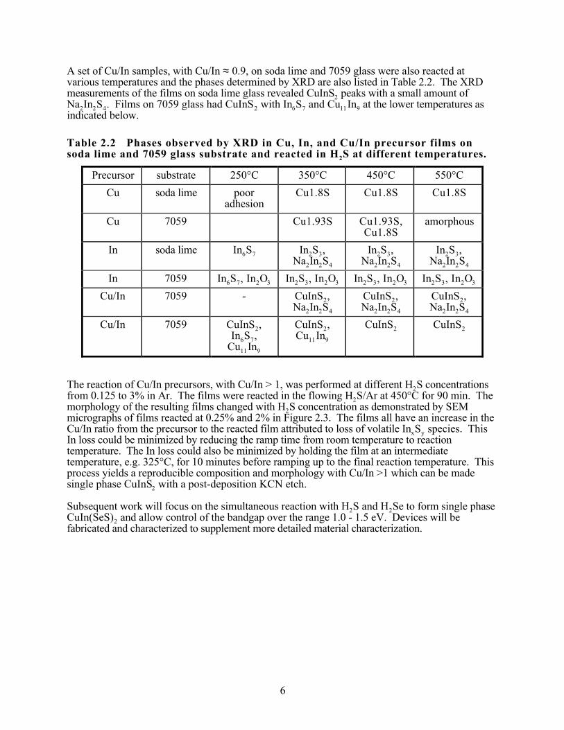
6
A set of Cu/In samples, with Cu/In ≈ 0.9, on soda lime and 7059 glass were also reacted atvarious temperatures and the phases determined by XRD are also listed in Table 2.2. The XRDmeasurements of the films on soda lime glass revealed CuInS2 peaks with a small amount ofNa2In2S4. Films on 7059 glass had CuInS2 with In6S7 and Cu11In9 at the lower temperatures asindicated below.
Table 2.2 Phases observed by XRD in Cu, In, and Cu/In precursor films onsoda lime and 7059 glass substrate and reacted in H2S at different temperatures.
Precursor substrate 250°C 350°C 450°C 550°CCu soda lime poor
adhesionCu1.8S Cu1.8S Cu1.8S
Cu 7059 Cu1.93S Cu1.93S,Cu1.8S
amorphous
In soda lime In6S7 In2S3,Na2In2S4
In2S3,Na2In2S4
In2S3,Na2In2S4
In 7059 In6S7, In2O3 In2S3, In2O3 In2S3, In2O3 In2S3, In2O3
Cu/In 7059 - CuInS2,Na2In2S4
CuInS2,Na2In2S4
CuInS2,Na2In2S4
Cu/In 7059 CuInS2,In6S7,
Cu11In9
CuInS2,Cu11In9
CuInS2 CuInS2
The reaction of Cu/In precursors, with Cu/In > 1, was performed at different H2S concentrationsfrom 0.125 to 3% in Ar. The films were reacted in the flowing H2S/Ar at 450°C for 90 min. Themorphology of the resulting films changed with H2S concentration as demonstrated by SEMmicrographs of films reacted at 0.25% and 2% in Figure 2.3. The films all have an increase in theCu/In ratio from the precursor to the reacted film attributed to loss of volatile InxSy species. ThisIn loss could be minimized by reducing the ramp time from room temperature to reactiontemperature. The In loss could also be minimized by holding the film at an intermediatetemperature, e.g. 325°C, for 10 minutes before ramping up to the final reaction temperature. Thisprocess yields a reproducible composition and morphology with Cu/In >1 which can be madesingle phase CuInS2 with a post-deposition KCN etch.
Subsequent work will focus on the simultaneous reaction with H2S and H2Se to form single phaseCuIn(SeS)2 and allow control of the bandgap over the range 1.0 - 1.5 eV. Devices will befabricated and characterized to supplement more detailed material characterization.

7
HOOD BOUNDARY
To pump
Ar cylinder
H Se mixcylinder
flow limiter
Ar purge
2Quartz Tube Heating Mantle
check valves
MFC 3
To Blower Air Velocity Detector
Waste Treatment
local area monitoring
Portable detector
To Hydrogen Selenide cylinder
Vacuum Pump
outlet
Substrate Holder
Pressure sensor shut-down for pressures>790 torr
Baratron Gauge
MFC 2
MFC1
argon
argon/ oxygen
argon/ hydrogen selenide
Ar/O cylinder
2
To Blower
To Stack
push-pull feedthrough
To RGA
Ion Gauge
Nitrogen Purge
Thermocouple Gauge
Turbo Pump
Argoncylinder
hydrogen sulfide
argon purge
H S2
flow limiter
purge
to p
ump
Hydrogen sulfide
MFC 4
Figure 2.1 Schematic diagram of the H2Se/H2S CVD reactor including gashandling and waste treatment.
1000
800
600
400
200
0
Coun
ts
5040302010
Two-Theta (degrees)
Na2In
2S
4
(003)Na
2In
2S
4
(014)
Na2In
2S
4
(108)
In2S
3
(109)
In2S
3
(103)
In2S
3
(0,0,12) In
2S
3
(206)
In2S
3
(1,0,15) In2S3
(2,2,12)
In/SLG
In/7059
Figure 2.2 XRD scans of In films on 7059 (top) and soda lime (bottom)substrates after they were reacted in H2S at 550°C for 90 min.

8
2% H2S concentration 0.25% H2S concentration
Figure 2.3 SEM micrographs at 2000x magnification showing the change inmorphology of Cu/In films reacted at different H2S concentrations.
2 .1 .4 Cu(InAl)Se2
The band gap of Cu(InAl)Se2 can be varied from 1.0 eV to 2.7 eV by varying the Al/(Al+In) ratiofrom 0 to 1.0. This steep variation of band gap in this alloy system can be exploited to achieve theoptimum band gap for an absorber of approximately 1.4 eV by replacing only 25 % of In by Al inCuInSe2. In contrast, about 60% of In has to be replaced by Ga to obtain 1.4 eV in theCu(InGa)Se2 system. In analogy with Cu(InGa)Se2, it may be preferable to replace as small an Incontent as possible in order to retain better device performance. Other practical advantages ofusing Al over other materials in current use for engineering the band gap, such as Ga and S, are theavailability and ease of handling. Also, it is easier to sputter deposit Al than Ga.
Existence of a continuous solid solution for the CuInSe2 - CuAlSe2 system has been established incrystal-form [109, 110, 111] and in thin film-form [112]. Powder diffraction studies have showedthat the lattice parameters vary linearly with ‘x’ in CuIn1-xAlxSe2 [110, 111]. The energy gap (Eg)is almost linear with ‘x’. The authors in Reference 111 have provided a relationship for thevariation of Eg with ‘x’ as:
Eg (x) = Eg (0) + bx(1-x) + [Eg (1)- Eg (0)]x : b = 0.51 (2.1)
2 .1 .4 .1 Experimental procedures
It was the goal of this work to obtain single phase Cu(InAl)Se2 thin films by selenization of Cu-Al-In precursors. The Cu thickness was chosen to be 2500 Å to obtain a final selenized film thicknessof approximately 2 µm. The precursors were deposited either by e-beam evaporation or bysputtering of individual elements on molybdenum coated soda lime glass substrates. There was nointentional heating of the substrates during the deposition of the precursors. The Al layer wasburied under either the In or Cu layer because Al would rapidly oxidize during transfer ofprecursors to the selenization reactor and the oxide layer would be very stable. Two sets ofprecursors were prepared: one set with Al/(Al+In) ratios 0.15, 0.30, and 0.45 and another setwith Al/(Al+In) ratios 0.05, 0.10, 0.15, and 0.20. Selenization was carried out at 450°C to 550°C

9
with a mixture of H2Se/Ar/O2 flowing. Selenized films were characterized by SEM, EDS andXRD.
2 .1 .4 .2 Results
For the precursor stacking sequence Cu/Al/In only elemental phases Cu, Al and In were observedin the as-deposited state. The Al layer between the Cu and In layers prevents alloying of Cu andIn. Al and In forms a eutectic and have very little solid solubility in each other. Cu-Al form aseries of intermetallic compounds: Cu9Al4, CuAl2, Cu3Al2, Cu4Al and Cu3Al. After annealing at450°C for 10 minutes the precursor with Al/(Al+In) ratio of 0.45 contain Cu9Al4 and In, theprecursor with Al/(Al+In) ratio of 0.30 contains Cu9Al4, Cu-Al solid solution and In, and theprecursor with Al/(Al+In) ratio of 0.15 contain Cu-Al solid solution and In. These results indicatethat Cu-Al alloys form preferably over Cu-In alloys.
Films obtained by selenizing Cu/Al/In precursors with Al/(Al+In) ratios 0.15, 0.30 and 0.45 at450°C for 90 minutes are non-uniform with In-rich regions. In-rich regions form during the ramp-to-reaction temperature due to the high surface mobility of In atoms. Due to preferential formationof Cu-Al alloys over Cu-In alloys, most of the In is present in the elemental form. Elemental In isable to diffuse rapidly on the surface to form islands of In. This non-uniformity in In distributionpresent after the ramp-to-reaction temperature gives rise to the compositional non-uniformity in theselenized films.
Films obtained by selenizing Al/Cu/In at 450°C precursors with Al/(Al+In) ratios 0.15, 0.30 and0.45 were also found to be non-uniform. XRD revealed that in all of the above selenized filmsCuInSe2 phase was predominant with a signature of CuAlSe2 phase in some films. Someunidentified peaks were also observed in few films. Spot EDS analysis on cross-sections suggeststhe presence of unreacted Cu-Al alloy at the Mo/film interface. Selenization at 500°C yieldedresults similar to those observed at 450°C. Al/Cu/In precursors selenized at 550°C showed definiteformation of CuAlSe2 for Al/(Al+In) ratios 0.30 and 0.45. Films with Al/(Al+In) ratio of 0.15 didnot show the presence of CuAlSe2. To remove non-uniformity due to In agglomeration, theprecursors were exposed to H2Se during the ramp-to-reaction temperature. XRD scans of thesefilms, however, did not show single phase Cu(InAl)Se2. Figure 2.4 shows an XRD scan of a filmobtained by selenizing an Al/Cu/In precursor at 550°C for 90 minutes. The pattern reveals thepresence of two distinct phases, CuInSe2 and Cu(InAl)Se2 with Al/(In+Al) ≈ 0.55. Even afterpost-selenization annealing at 600°C for 60 minutes, a single phase Cu(InAl)Se2 film was notobtained.
Al/Cu/In precursors with Al/(Al+In) ratios of 0.05, 0.10, 0.15 and 0.20 were selenized at 550°Cfor 90 minutes with H2Se flowing during the ramp-to-reaction temperature. Figure 2.5 shows thedetailed XRD scans of the several characteristic peaks in the resulting films . The Al/(Al+In)ratios were chosen after realizing the difficulty in obtaining single phase at 550°C for 90 minutesreaction time for higher Al/(Al+In) ratios of 0.30 and 0.45. Selenization at 600°C was notattempted because soda-lime glass substrates soften and loose their mechanical integrity at thistemperature. In Figure 2.5(a)-(d) the X-ray peaks shift to higher angles, i.e., to lower d-spacings, with increasing Al content in the films. Due to the overlap of the Se ‘L’ and Al ‘K’ X-ray energies, EDS compositional measurements of these films were not accurate. The X-ray peakpositions of the film from the precursor with Al/(Al+In) of 5% indicates that this film containsCuInSe2 to a large extent with very little or no Al dissolved in the CuInSe2 phase. The other threefilms show a definite change in lattice parameter due to Al dissolution in CuInSe2. In Figure2.5(c), the peak shape of (312)/(116) changes from a doublet due to c/a ratio of a chalcopyritestructure different from 2.0 to a single peak due to a c/a ratio of 2.0. As the ‘x’ in CuIn1-xAlxSe2increases from 0 to 1.0 the c/a ratio of the resulting structure varies from 2.01 to 1.96.

10
In conclusion, single phase Cu(InAl)Se2 films were obtained by selenizing stacked metallic layersof Al/Cu/In in H2Se at 550°C for 90 minutes.
1000
800
600
400
200
0
Inte
nsit
y (C
oun
ts/2
s)
28.027.527.026.526.0
2θ
CIS
CIAS
(112)600
500
400
300
200
100
0
Inte
nsit
y (C
oun
ts/2
s)
56524844
2θ
CIS
CIAS
(220) (204)&
(312) (116)
CIS
CIAS
Figure 2.4 XRD pattern of a film obtained by selenizing Al/In/Cu precursorat 550°C. The Al/(Al+In) ratio in the precursor is ≈ 0 .45 .
CIS = CuInSe2, CIAS = CuIn1-xAlxSe2.

11
6000
5000
4000
3000
2000
1000
0
Inte
nsit
y (C
oun
ts/5
s)
27.427.227.026.826.626.426.226.0
(112)
5 % Al/(Al+In) 10 % Al/(Al+In) 15 % Al/(Al+In) 20 % Al/(Al+In)
a
3000
2000
1000
0
Inte
nsit
y (C
oun
ts/5
s)
45.545.044.544.043.5
(220) (204) 5 % Al/(Al+In) 10 % Al/(Al+In) 15 % Al/(Al+In) 20 % Al/(Al+In)
b
2000
1500
1000
500
0
Inte
nsit
y (C
oun
ts/5
s)
53.553.052.552.051.5
(312) (116) 5 % Al/(Al+In) 10 % Al/(Al+In) 15 % Al/(Al+In) 20 % Al/(Al+In)
c
600
500
400
300
200
100
0
Inte
nsit
y (C
oun
ts/5
s)
72.071.571.070.52θ
(332) (316)
5 % Al/(Al+In) 10 % Al/(Al+In) 15 % Al/(Al+In) 20 % Al/(Al+In)
d
Figure 2.5 XRD plots of various peaks of a CuIn1-xAlxSe2 films(from run L0393). The Al/Al+In) concentrations in the legends
are intended ratios in the precursors.

12
2.2 Reduced Cu(InGa)Se2 Deposition Temperature and Thickness
2 .2 .1 Introduction
There are many technical issues which need to be addressed to effectively enable the transfer ofCu(InGa)Se2 deposition and device fabrication technology from the laboratory to manufacturingscale. In general, these issues provide means to reduce thin film semiconductor process costs.Shorter deposition time can be achieved with reduced film thickness and increased deposition rate.Thinner absorber films reduce the total amount of material used and allow faster processthroughput. The minimum thickness of the Cu(InGa)Se2 absorber layer may be determined by thenucleation of the film to form a continuous layer or by the film morphology. From a deviceperspective, the minimum thickness may be determined by the minority carrier diffusion length andoptical absorption coefficient of the Cu(InGa)Se2 or the ability to incorporate optical confinement.
Lower substrate temperature (Tss) can lower processing costs by reducing thermally induced stresson the substrate, allowing faster heat-up and cool-down, and decreasing the heat load and stress onthe entire deposition system. In addition, with lower substrate temperature, stress on the glasssubstrate can be reduced and alternative substrate materials, like a flexible polymer web, could beutilized.
In this work, we have addressed the need to improve process throughput by reducing theCu(InGa)Se2 thickness and deposition temperature. The approach during this work has been tofirst define a baseline process for Cu(InGa)Se2 deposition by multisource elemental evaporationand solar cell fabrication. All other deposition parameters are then held fixed to determine theeffects of varying either the substrate temperature or, by changing the deposition time, filmthickness. Material properties of the resulting Cu(InGa)Se2 films have been characterized and theirdevice behavior has been measured and analyzed.
2 .2 .2 Experimental procedures
Cu(InGa)Se2 films were deposited by thermal evaporation from four elemental sources. Details ofthe deposition, film characterization, and device fabrication are described in Reference 101. Thebaseline deposition process in this work is the same as described but with Tss maintained constantthrough the entire deposition. The films are deposited with a Cu-rich first layer, deposited in 32min. and followed continuously by an In-Ga-Se second layer deposited in 12 min. The fluxes ofGa and In are constant through the deposition time so there is no grading of the bandgap. A profileof the source and substrate temperatures are shown in Figure 2.6. This results in ~2.5 µm thickfilms with Ga/(In+Ga) ≈ 0.3 which gives a bandgap ~ 1.2 eV.
To study the effect of substrate temperatures, Cu(InGa)Se2 films were deposited with Tss from 600to 350°C, maintaining fixed source effusion rates and deposition times. To study varyingthicknesses, films were deposited with constant effusion rates and Tss, and only the times adjusted.
The film thickness was determined by the mass gain after deposition and from cross-sectionalmicrographs and the films were characterized by scanning electron microscope (SEM) images,energy dispersive x-ray spectroscopy (EDS), x-ray diffraction (XRD). Secondary ion massspectroscopy (SIMS) measurements were performed at NREL.
The Cu(InGa)Se2 films were deposited on soda lime glass substrates with a sputtered 1 µm thickMo layer. Complete solar cells were fabricated [101] with the chemical bath deposition of ~ 30 nmCdS followed by rf sputtered ZnO:Al with thickness 0.5 µm and sheet resistance 20 Ω/sq. Twodifferent cell configurations were used. Cells with active area ≈ 0.13 cm2 were fabricated bydeposition of Ni bus bar/contact tabs and mechanical scribing to define cell areas. Cells with total
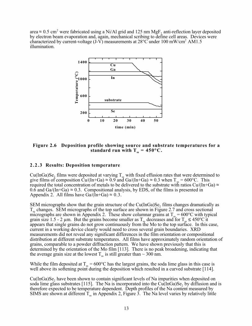
13
area ≈ 0.5 cm2 were fabricated using a Ni/Al grid and 125 nm MgF2 anti-reflection layer depositedby electron beam evaporation and, again, mechanical scribing to define cell areas. Devices werecharacterized by current-voltage (J-V) measurements at 28°C under 100 mW/cm2 AM1.5illumination.
200
600
1000
1400
0 10 20 30 40 50
Tem
pera
ture
(°C
)
time (min)
CuGa
In
substrate
Se
Figure 2.6 Deposition profile showing source and substrate temperatures for astandard run with Tss = 450°C.
2 .2 .3 Results: Deposition temperature
Cu(InGa)Se2 films were deposited at varying Tss with fixed effusion rates that were determined togive films of composition Cu/(In+Ga) ≈ 0.9 and Ga/(In+Ga) ≈ 0.3 when Tss = 600°C. Thisrequired the total concentration of metals to be delivered to the substrate with ratios Cu/(In+Ga) ≈0.6 and Ga/(In+Ga) ≈ 0.3. Compositional analysis, by EDS, of the films is presented inAppendix 2. All films have Ga/(In+Ga) ≈ 0.3.
SEM micrographs show that the grain structure of the Cu(InGa)Se2 films changes dramatically asTss changes. SEM micrographs of the top surface are shown in Figure 2.7 and cross sectionalmicrographs are shown in Appendix 2. These show columnar grains at Tss = 600°C with typicalgrain size 1.5 - 2 µm. But the grains become smaller as Tss decreases and for Tss ≤ 450°C itappears that single grains do not grow continuously from the Mo to the top surface. In this case,current in a working device clearly would need to cross several grain boundaries. XRDmeasurements did not reveal any significant differences in the film orientation or compositionaldistribution at different substrate temperatures. All films have approximately random orientation ofgrains, comparable to a powder diffraction pattern. We have shown previously that this isdetermined by the orientation of the Mo film [113]. There is no peak broadening, indicating thatthe average grain size at the lowest Tss is still greater than ~ 300 nm.
While the film deposited at Tss = 600°C has the largest grains, the soda lime glass in this case iswell above its softening point during the deposition which resulted in a curved substrate [114].
Cu(InGa)Se2 have been shown to contain significant levels of Na impurities when deposited onsoda lime glass substrates [115]. The Na is incorporated into the Cu(InGa)Se2 by diffusion and istherefore expected to be temperature dependent. Depth profiles of the Na content measured bySIMS are shown at different Tss in Appendix 2, Figure 3. The Na level varies by relatively little

14
from 400 to 600°C and is actually highest for the lowest Tss, though diffusion of Na is expected toincrease with increasing Tss. This may be explainable by Na diffusion along grain boundariessince there is a greater grain boundary density at the lower temperature. The SIMS profiles for Cu,Ga, In, Se, Mo, and Na are shown in Figure 2.8 for samples deposited at Tss = 600, 500, and400°C. These profiles show that the Cu, In, and Ga are uniformly distributed from the frontsurface of the film to the Mo contact at all deposition temperatures.
Finally, solar cells were fabricated with films deposited at varying Tss and the J-V parameters forthe best cell achieved at each Tss are listed in Table 2.3. The efficiency (η) decreases slowly as Tssdecreases from 550°C, but is still 12.8% at 400°C and 10.9% at 350°C. While there is sometradeoff in Voc and Jsc which may be associated with variations in the Ga content and, therefore,bandgap of the Cu(InGa)Se2, the biggest change is the fill factor. Further analysis of these devicesis presented in Section 2.2.5.
The dependence of grain size with Tss has been reported previously [116] and at high temperatureswas attributed to the formation of copper selenide phases above ~525°C which act as a “flux” forgrain growth in the Cu rich film [117]. However, the films in this work show an increasing grainsize with increasing Tss over the entire temperature range. There is only a small drop-off in deviceperformance with lower Tss despite the decreasing grain size.
Table 2.3 J-V parameters with varying substrate temperature.
Tss Voc Jsc FF η
(°C) (mV) (mA/cm2) (%) (%)600 0.596 31.2 67.4 12.5550 0.583 34.3 71.8 14.4500 0.606 32.5 70.0 13.8450 0.605 32.6 68.4 13.5400 0.606 32.5 64.8 12.8350 0.561 33.2 58.6 10.9
Tss = 600°C Tss = 500°C Tss = 400°C
Figure 2.7 SEM micrographs showing a decrease in grain size as Tss decreasesfrom 600 to 400°C.

15
101
102
103
104
105
106
0 300 600 900 1200 1500
seco
ndar
y io
n co
unts
sputter time (min)
CuMo
Na
Ga
Se
In
600°C
(a)
101
102
103
104
105
106
0 300 600 900 1200 1500
seco
ndar
y io
n co
unts
sputter time (min)
Cu Mo
Na
Ga
Se
In
500°C
(b)
101
102
103
104
105
106
0 300 600 900 1200 1500
seco
ndar
y io
n co
unts
sputter time (min)
CuMo
Na
Ga
Se
In
400°C
(c)
Figure 2.8 SIMS depth profiles of Cu, In, Ga, Se, Mo, and Na for filmsdeposited with (a) Tss = 600°C, (b) 500°C, and (c) 400°C.

16
2 .2 .4 Results: Film thickness
Using the same effusion rates as above, the effect of thickness has been studied by changing thedeposition times with Tss = 450°C to give films with thickness (d) ranging from 2.5 to 1.0 µm asdetermined by mass gain of the substrate. The thickness estimated from SEM cross-sectionalmicrographs was ~ 0.2 µm thinner than that determined from the mass gain. The composition ofthese films was unchanged over the thickness range with all films having Cu/(In+Ga) ≈ 0.9 andGa/(In+Ga) ≈ 0.3 and again, no difference in orientation or compositional distribution wasobserved by XRD.
Device results for different Cu(InGa)Se2 thickness with this deposition process are shown in Table2.4. With d ≥ 1.4 µm the devices have η ≈ 13%. There are no significant thickness related losseswhich might include effects of bulk series resistance or back surface recombination. For d = 1.0µm, η decreases due to decreases in Voc, Jsc, and FF. In addition, the J-V curves both in the darkand under illumination indicate an increased shunt conductance for the thinnest cells. SEMmicrographs in Section 2.2.3 and Appendix 2 show that films deposited with Tss < 500°C havedecreasing grain size and horizontal grain boundaries. This may lead to morphological defectswhich contribute shunt-like characteristics to the J-V behavior of the cells with thinnerCu(InGa)Se2 layers.
Table 2.4 J-V parameters with decreasing Cu(InGa)Se2 thickness for filmsdeposited at Tss = 450°C.
d ± 0.2 Voc Jsc FF η(µm) (mV) (mA/cm2) (%) (%)2.5 0.605 32.6 68.4 13.51.8 0.581 33.7 66.6 13.01.4 0.590 32.5 69.5 13.31.2 0.526 34.2 64.9 11.71.0 0.514 30.7 62.5 9.9
2 .2 .5 Device measurements and analysis
For the six evaporation runs made on which results were reported in Table 2.3, a total of 101devices from 19 samples were processed and tested. Twenty-four samples of six cells each for atotal of 144 devices were processed and tested from the 10 evaporation runs made at five differentCu(In,Ga)Se2 thicknesses.
In addition, Table 2.5 and Table 2.6 show the averaged J-V parameters, along with their standarddeviation, taken from the highest efficiency test for every sample processed from these evaporationruns. These results include cells with area ≈ 0.13 cm2 tested on an active area basis, and cells witharea ≈ 0.42 cm2 tested on a total area basis. Furthermore, some cells have an MgF2 anti-reflectionlayer. Although the samples were not processed at identical times or under identical conditionsafter the Cu(In,Ga)Se2
evaporation runs, they still give an idea of the sample to sample variation,and the cell to cell variation within a sample, that can occur. There would have been an even widervariation if the heavily shunted or shorted devices not been excluded.
The statistical data shown in Table 2.5 and Table 2.6 show a great deal of overlap in the J-Vparameters as a function of either thickness or substrate temperature. However, it can be seen thatthe averaged efficiency does fall off at the two lowest thicknesses (1.0 and 1.2 µm) and the lowest

17
substrate temperature (350°C). In all of these cases there is a decrease in FF due to an increase inshunting behavior as shown in the values of dJ/dV@Jsc. The shunting behavior was also seen inthe dark J-V characteristic. The shunting behavior could lead to a decrease in Voc as well. Thiscould be caused by the rougher and thinner Cu(In,Ga)Se2 material. The loss in Jsc for thinnerCu(InGa)Se2 cannot be explained by simple morphology.
It is necessary to improve the uniformity of device results within a single Cu(In,Ga)Se2evaporation run before more detailed differences can be seen.
Table 2.5 Statistics of all the device J-V parameters for each sample made intocells as a function of substrate temperature. Parameters were taken from the bestaverage efficiency test. *Shorted or heavily shunted (dJ/dV@Jsc > 25 mS/cm2)not included in the statistics.
Substrate Average ± Standard Deviation # of totalTemp. Efficiency JSC Voc FF dV/dJ@Voc dJ/dV@Jsc good # of
(°C) (%) (mA/cm2) (V) (%) (Ω-cm2) (mS/cm2) cells* cells Test Date Sample #
600 14.56±0.34 33.4±0.3 0.610±0.003 71.4±0.9 1.5±0.0 2.4±0.5 5 5 22-May-97 32774-32600 12.41±1.09 31.9±0.9 0.600±0.010 64.9±5.4 2.0±0.3 2.4±1.3 4 6 22-May-97 32774-33600 11.39±0.91 30.7±0.3 0.593±0.011 62.6±4.0 2.2±0.2 3.5±0.7 4 6 11-Apr-97 32774-23600 10.69±0.55 28.7±0.3 0.625±0.009 59.6±2.6 2.8±0.3 3.8±0.4 5 6 12-Jun-97 32774-22
550 13.74±0.68 32.9±1.3 0.585±0.002 71.4±0.7 1.7±0.1 1.1±0.6 6 6 22-Sep-97 32808-32550 11.47±0.48 29.3±0.4 0.566±0.009 69.2±0.9 1.9±0.0 1.5±0.9 6 6 16-Sep-97 32808-23
500 13.22±0.42 32.0±0.6 0.603±0.004 68.6±0.8 1.8±0.1 1.8±0.5 3 3 20-May-97 32773-32500 12.78±0.20 30.2±0.1 0.606±0.002 69.9±0.9 1.8±0.0 2.3±1.1 6 6 18-Apr-97 32773-33500 11.58±0.44 29.6±0.6 0.598±0.003 65.3±1.3 2.3±0.0 3.6±1.6 6 6 16-Apr-97 32773-23
450 12.85±0.51 31.3±0.9 0.600±0.006 68.5±1.0 1.9±0.1 1.8±0.6 6 6 19-Sep-97 32797-33450 10.01±1.18 29.4±1.6 0.539±0.019 62.9±2.5 2.6±0.4 2.7±0.6 6 6 16-Sep-97 32797-23
400 13.09±0.69 34.4±0.6 0.603±0.004 63.0±3.2 2.1±0.1 7.0±3.6 6 6 22-May-97 32771-23400 12.32±0.42 31.2±1.2 0.611±0.002 64.7±0.9 2.4±0.2 2.6±0.3 3 3 20-May-97 32771-23400 12.15±0.39 31.6±0.9 0.585±0.003 65.8±0.8 2.3±0.0 2.7±1.2 4 5 12-Jun-97 32771-22400 11.93±0.48 30.0±1.1 0.587±0.004 67.7±0.6 1.9±0.0 2.6±0.8 5 6 20-May-97 32771-33400 11.78±1.40 32.0±0.9 0.576±0.008 63.7±5.0 2.1±0.3 4.1±1.7 2 4 11-Apr-97 32771-32400 10.77±0.40 27.9±0.3 0.580±0.002 66.6±1.8 2.0±0.1 3.7±1.0 6 6 05-Jun-97 32771-13
350 10.56±0.21 33.4±0.8 0.557±0.013 56.8±1.2 2.5±0.1 5.7±0.2 2 3 20-May-97 32780-33350 0 6

18
Table 2.6 Statistics of all the device J-V parameters for each sample made intocells as a function of Cu(InGa)Se2 thickness. Parameters were taken from thebest average efficiency test. *Shorted or heavily shunted (dJ/dV @ Jsc > 25mS/cm2) not included in the statistics.
Thick- Average ± Standard Deviation # of totalness Efficiency JSC Voc FF dV/dJ@Voc dJ/dV@Jsc good # of
(µm) (%) (mA/cm2) (V) (%) (Ω-cm2) (mS/cm2) cells* cells Test Date Sample #
2.5 12.85±0.51 31.3±0.9 0.600±0.006 68.5±1.0 1.9±0.1 1.8±0.6 6 6 19-Sep-97 32797-332.5 12.39±0.54 32.1±1.3 0.572±0.004 67.6±0.9 1.8±0.0 2.3±1.0 5 6 28-Aug-97 32798-322.5 11.39±0.77 30.5±0.7 0.558±0.010 66.9±3.5 1.9±0.1 3.7±4.5 6 6 28-Aug-97 32798-232.5 10.01±1.18 29.4±1.6 0.539±0.019 62.9±2.5 2.6±0.4 2.7±0.6 6 6 16-Sep-97 32797-23
1.8 12.90±0.78 33.2±1.7 0.582±0.003 66.9±0.8 1.8±0.2 2.4±1.3 4 6 16-Sep-97 32800-231.8 11.78±1.90 33.1±1.4 0.552±0.008 64.3±8.4 1.9±0.4 6.0±7.8 5 6 16-Sep-97 32801-321.8 10.59±0.41 30.0±0.6 0.546±0.006 64.7±2.2 2.2±0.2 2.7±1.8 6 6 10-Sep-97 32800-131.8 10.55±0.12 29.4±0.2 0.522±0.001 68.6±0.4 1.9±0.0 2.0±0.7 5 6 5-Sep-97 32801-231.8 9.90±0.30 28.6±0.2 0.527±0.006 65.6±0.9 2.2±0.0 3.0±1.0 6 6 11-Sep-97 32801-131.8 0 6 5-Sep-97 32800-32
1.4 13.12±0.12 32.1±0.2 0.594±0.000 68.8±0.7 1.9±0.1 1.8±1.2 3 6 20-May-97 32777-321.4 11.42±0.41 31.5±0.3 0.558±0.005 65.0±1.8 2.2±0.0 3.1±1.8 5 6 16-Apr-97 32776-231.4 10.90±0.55 30.3±0.0 0.543±0.004 66.4±2.8 2.0±0.0 3.4±2.9 4 6 15-Apr-97 32777-231.4 10.25±2.42 31.3±0.7 0.528±0.033 61.2±11.4 2.7±1.3 4.8±6.7 6 6 16-Apr-97 32776-32
1.2 10.64±0.51 31.7±1.2 0.509±0.004 66.0±2.2 1.8±0.0 4.1±2.9 6 6 16-Sep-97 32802-231.2 10.50±1.00 31.7±2.4 0.525±0.005 63.0±2.1 2.1±0.2 5.5±1.8 6 6 19-Sep-97 32806-32
1.2 8.71±0.42 28.6±0.6 0.483±0.005 63.1±1.5 2.2±0.1 5.2±1.8 5 6 10-Sep-97 32802-131.2 8.17±0.76 28.0±0.6 0.479±0.011 61.0±5.2 2.5±0.2 7.0±6.6 6 6 12-Sep-97 32806-231.2 7.16±1.04 28.5±0.8 0.434±0.038 57.6±2.0 2.3±0.0 10.8±1.9 4 6 8-Sep-97 32802-32
1.0 9.10±0.62 28.8±1.4 0.507±0.009 62.3±3.1 2.7±0.6 5.6±2.1 6 6 16-Sep-97 32803-131.0 8.63±0.68 27.9±1.3 0.489±0.013 63.2±2.4 2.3±0.2 5.0±2.0 6 6 15-Sep-97 32805-231.0 8.46±0.63 29.3±1.4 0.482±0.007 60.0±4.3 2.1±0.2 7.6±1.7 6 6 8-Sep-97 32803-231.0 4.96±0.76 27.8±1.1 0.367±0.038 48.6±2.9 3.1±0.5 18.2±3.8 3 6 15-Sep-97 32805-321.0 0 6 8-Sep-97 32803-32
2.3 Teaming Results
2 .3 .1 Introduction
IEC is a member of the National CIS Team under the NREL Thin Film Partnership Program. TheCIS Team effort includes four working groups (WG). Of these, IEC has been a member of theTransient Effects WG and the New Junction WG, for which William Shafarman is the GroupLeader. The work done at IEC for each of these Working Groups is described below.
2 .3 .2 New junction results
The New Junction WG has identified two tasks and IEC has contributed to work on each. Theobjective of the first task is to develop non-cadmium containing buffer layers. The priority is on

19
vacuum processes which could potentially be incorporated in-line and chemical bath deposition isnot considered a primary option. The objective of the second task is to develop improved TCOlayers to minimize losses for module fabrication and quantify the effect of TCO layers on moduleperformance. This task is focusing on the high conductivity TCO layers.
For the first task, IEC provided device fabrication and J-V and QE measurements forCu(InGa)Se2/ZnO samples provided by other team members. This included ZnO layers depositedby MOCVD at Washington State University (WSU), by dc reactive sputtering at University ofSouth Florida (USF), and by rf sputtering from a ZnO:Al2O3 target. Samples were processed withand without a solvent/water rinse prior to ZnO deposition. These layers were deposited onCu(InGa)Se2 films provided by NREL and EPV. Device completion included deposition of ourbaseline ZnO:Al, deposition of Ni contacts or a Ni/Al grid, and mechanical scribing. IEC also didexperiments to compare the effect of sputtering from a ZnO:Al2O3 target in different atmospheres.
A summary of the J-V tests on Cu(InGa)Se2/ZnO cells completed at IEC is given in Table 2.7. Inthe table, Roc is the slope dV/dJ at J = 0 and Gsc is the slope dJ/dV at V = 0. All measurements inthis case are active area results with no AR layers on the cells. The results include aCu(InGa)Se2/ZnO device with the MOCVD i-ZnO from WSU on Cu(InGa)Se2 deposited at NRELwith 13.9% efficiency. J-V and QE curves for this device and a description of the process for thei-ZnO deposition for are described in [118]. The growth includes an initial growth step at 250°Cwith flowing hydrogen. An additional set of 10 samples with the MOCVD i-ZnO on absorberlayers from NREL and SSI, completed and tested at IEC, showed that this first step was necessaryfor good device performance [118].
Results shown in Table 2.7 where the i-ZnO layers were deposited by EPV in Ar:O2 indicateshorted devices while i-ZnO deposited in Ar:H2 gave up to η = 9%. An experiment to determinewhether the H2 plays a beneficial role in this process or whether merely the absence of O2 in thesputter gas is critical was addressed in a set of devices fabricated completely at IEC. Previousresults with a high resistivity (~100 Ω-cm) ZnO buffer layer deposited by sputtering from theZnO:Al2O3 target in Ar/O2 with 2% O2 gave shorted devices. Devices were fabricated withabsorber films from a single deposition of evaporated Cu(InGa)Se2 with Ga/(In+Ga) ≈ 0.25. ZnOlayers were sputtered in either pure Ar or Ar:H2 with 4% H2. All cells, including a control samplewith a CdS buffer layer deposited by CBD, had a 0.5 µm thick ZnO layer sputtered in Ar as theprimary TCO layer deposited on top of the buffer layer. In each case, the best device had η = 8%as shown in Table 2.8, while the control sample gave η = 13%. The Cu(InGa)Se2/ZnO sampleshad poor reproducibility over the 12 devices on two pieces with each buffer layer, primarily due toshunting in the dark and illuminated J-V characteristics. These preliminary results show noadvantage to the presence of H2.
Under the second task, “Improved TCO Layers,” the New Junction WG has focused on anobserved increase in ZnO sheet resistance when it is deposited on CdS. This was shown at IECfor different TCO materials deposited on glass and glass/CdS substrates. The samples includesingle layer low resistivity ZnO:Al, bi-layer high /low resistivity ZnO:Al, and ITO. The CdS wasour standard CBD film deposited in a double dip to give thickness ~70 nm The average sheetresistance of each sample type is given in Table 2.9. In each case the resistance of the ZnOdeposited on CdS is higher than that deposited on bare glass. Optical transmission and reflectionof each sample were also measured at IEC. These samples were sent for FTIR, atomic forcemicroscopy, and Hall effect measurements at the Universities of Florida and South Florida.
Two different experiments at IEC confirmed that the increase in ZnO resistance also occurs whenthe CdS/ZnO layers are deposited on Cu(InGa)Se2. The sheet resistance of the ZnO in a completeglass/Mo/Cu(InGa)Se2/CdS/ZnO structure was measured on working devices. This was done byfabricating devices with two separate Ni contact tabs deposited on the ZnO and measuring the J-Vcurve between them with a bias voltage maintained between the front of the device and the Mo back

20
contact. The tab-to-tab resistance does not change with the bias voltage confirming that there is nosignificant leakage through the device and the measured resistance is due to the ZnO. The sheetresistance is then given by
Rsq = Rtab −to− tablw
(2.2)
where l = 0.52 cm is the cell width and w = 0.25 cm is the spacing between the contact tabs. On atypical device, #32744.32, for which the ZnO witness slide gave Rsq = 18 Ω/sq, the tab-to-tabmeasurement in the device gave Rsq = 29 Ω/sq, similar to the increase seen on the glass/CdSsamples.
Table 2.7 J-V parameters for Cu(InGa)Se2/ZnO devices completed and tested atIEC.
Cu(InGa)Se2 i-ZnO Best Cellpc. # pre-rinse source process Voc
(V)Jsc
(mA/cm2)FF(%)
eff(%)
Roc
(Ω -cm2)Gsc
(mS/cm2)
NREL 675-2 yes WSU MOCVD 0.529 33.1 55.6 9.7 2.3 10.NREL 679-9 yes WSU MOCVD 0.524 33.5 69.5 12.2 1.6 1.EPV 716-3-1 yes WSU MOCVD shortedEPV 709-1-1 yes WSU MOCVD 0.411 33.5 62.5 8.6 1.5 6.NREL681-5 - WSU MOCVD 0.267 25.4 32.7 2.2 6.4 50.NREL 679-5 yes WSU MOCVD 0.581 34.5 69.2 13.9 1.9 2.EPV 716-3-2 yes WSU MOCVD 0.426 37.1 61.0 9.6 1.5 6.EPV 709-1-2 - WSU MOCVD 0.412 37.7 56.3 8.8 2.0 6.
NREL 681-4 yes USF react-sp 0.082 21.8 29.3 0.5 2.8 180NREL 680-8 - USF react-sp 0.083 2.9 28.1 0.1 21.4 29EPV 709-2-6 yes USF react-sp 0.085 24.3 28.1 0.6 2.8 225EPV 709-1-5 - USF react-sp 0.115 18.8 29.6 0.6 4.3 120
EPV 709-2-1 yes EPV sput Ar:O2 shortedNREL 680-3 yes EPV sput Ar:O2 shortedEPV 709-2-4 - EPV sput Ar:O2 shortedNREL 680-4 - EPV sput Ar:O2 flaked offEPV 709-2-3 yes EPV sput Ar:H2 0.127 23.9 33.3 1.0 3.0 96.EPV 706-3-3 yes EPV sput Ar:H2 0.107 22.5 32.9 0.8 2.8 112.NREL 679-8 yes EPV sput Ar:H2 0.386 26.4 45.5 4.6 3.7 16.EPV 709-2-2 - EPV sput Ar:H2 0.125 25.0 31.4 1.0 3.3 123.NREL 679-4 - EPV sput Ar:H2 0.501 29.2 62.0 9.1 2.1 2.

21
Table 2.8 Device results with ZnO buffer layers deposited on Cu(InGa)Se2 in Arand Ar:H2 sputter gases.
pc. # CdS ZnO:Aldeposition
Voc(V)
Jsc(mA/cm2)
FF(%)
η(%)
32814.21 CdS Ar 0.560 31.1 73.2 12.732814.22 none Ar 0.538 24.3 61.8 8.132814.11 none Ar:H2 0.488 26.1 61.2 7.8
Table 2.9 Sheet resistances of different TCO materials deposited on glass andglass/CdS substrates.
Rsq (Ω/sq)TCO on glass on glass/CdS
bi-layer ZnO 18 25single layer ZnO 26 35
ITO 20 30
2 .3 .3 Transient Effects
2 .3 .3 .1 Introduction
The CuInSe2 thin film partnership program organized a transient effects team to determine ifpresent I-V testing procedures can predict the daily output of CuInSe2-based modules and cellsunder field conditions; and, if they cannot, determine what new testing procedures are needed.
2 .3 .3 .2 Initial Tests
As a start, it was decided to stress (with temperature, illumination and electrical bias) one of IEC'sCu(In,Ga)Se2 devices for a period of hours and monitor its recovery.
This device stressed at a temperature of 80°C with and without illumination (approximately88 mW/cm2) under various conditions of electrical bias (-0.5 V, 0.0 V, ~ maximum power,0.0 mA/cm2 and +30 mA/cm2). After each stress, the illumination and voltage bias was removedand they were brought to room temperature in about 3 minutes. Their recovery was monitored bymeasuring and analyzing their J-V behavior at three different light intensities plus dark atlogarithmically spaced time intervals.
The IEC Cu(InGa)Se2 device (IEC-32702-32-7) was put through this stress sequence. Over thetime it was stressed and monitored, the only significant change was the development of a shuntwhen held in reverse bias. The J-V results of these stress tests are shown in Figure 2.9 to Figure2.16.

22
25
30
35
1 10 100 1000
J SC [m
A/c
m2 ]
time [min]
Pre stress
0.5
0.55
0.6
0.65
0.7
1 10 100 1000
Voc
[V]
time [min]
Pre stress
(a) (b)
60
65
70
75
80
1 10 100 1000
FF [%
]
time [min]
Pre stress
10
15
20
1 10 100 1000
Effic
ienc
y [%
]
time [min]
Pre stress
(c) (d)
Figure 2.9 Jsc, V oc, FF and efficiency vs. recovery time for device IEC-32702-32-7 after stress at a temperature of 80°C, in the dark and 0 V for 12 hours.

23
25
30
35
1 10 100 1000
J SC [m
A/c
m2 ]
time [min]
Pre stress
0.5
0.55
0.6
0.65
0.7
1 10 100 1000
V OC [V
]
time [min]
Pre stress
(a) (b)
60
65
70
75
80
1 10 100 1000
FF [%
]
time [min]
Pre stress
10
15
20
1 10 100 1000
Effic
ienc
y [%
]
time [min]
Pre stress
(c) (d)
Figure 2.10 Jsc, V oc, FF and efficiency vs. recovery time for deviceIEC-32702-32-7 after stress at a temperature of 80°C,
in the dark and at a forward current of 30 mA/cm2 for 10 hours.

24
25
30
35
1 10 100 1000
J SC [m
A/c
m2 ]
time [min]
Pre stress
0.5
0.55
0.6
0.65
0.7
1 10 100 1000
Voc
[Vol
ts]
time [min]
Pre stress
(a) (b)
60
70
80
1 10 100 1000
FF [%
]
time [min]
Pre stress
10
15
20
1 10 100 1000
Effic
ienc
y [%
]
time [min]
Pre stress
(c) (d)
Figure 2.11 Jsc, V oc, FF and efficiency vs. recovery time for deviceIEC-32702-32-7 after stress at a temperature of 80°C,
in the dark and at V = -0.5 V for 12 hours.*
* Still shunted from a previous stress test.

25
25
30
35
1 10 100 1000
J SC [m
A/c
m2 ]
time [min]
Pre stress
0.5
0.55
0.6
0.65
0.7
1 10 100 1000
V OC [V
]
time [min]
Pre stress
(a) (b)
60
65
70
75
80
1 10 100 1000
FF [%
]
time [min]
Pre stress
10
15
20
1 10 100 1000
Effic
ienc
y [%
]
time [min]
Pre stress
(c) (d)
Figure 2.12 Jsc, V oc, FF and efficiency vs. recovery time for deviceIEC-32702-32-7 after stress at a temperature of 80°C,
AM1 illumination and at a forward currentof mA/cm2 for 12 hours.

26
10
15
20
1 10 100 1000
Effic
ienc
y [%
]
time [min]
Pre stress
0.5
0.55
0.6
0.65
0.7
1 10 100 1000
Voc
[Vol
ts]
time [min]
Pre stress
(a) (b)
60
65
70
75
80
1 10 100 1000
FF [%
]
time [min]
Pre stress
10
15
20
1 10 100 1000
Effic
ienc
y [%
]
time [min]
Pre stress
(c) (d)
Figure 2.13 Jsc, V oc, FF and efficiency vs. recovery time for deviceIEC-32702-32-7 after stress at a temperature of 80°C,
AM1 illumination and at V = -0.5 V for 12 hours.*
* Shunt developed during stress test.

27
25
30
35
1 10 100 1000
J SC [m
A/c
m2 ]
time [min]
Pre stress
0.5
0.55
0.6
0.65
0.7
1 10 100 1000
V OC [V
]
time [min]
Pre stress
(a) (b)
60
65
70
75
80
1 10 100 1000
FF [%
]
time [min]
Pre stress
10
15
20
1 10 100 1000
Effic
ienc
y [%
]
time [min]
Pre stress
(c) (d)
Figure 2.14 Jsc, V oc, FF and efficiency vs. recovery time for deviceIEC-32702-32-7 after stress at a temperature of 80°C,AM1 illumination and RL = 12.6 Ω-cm 2 for 10 hours.

28
25
30
35
1 10 100 1000
J SC [m
A/c
m2 ]
time [min]
Pre stress
0.5
0.55
0.6
0.65
0.7
1 10 100 1000
V OC [V
]
time [min]
Pre stress
(a) (b)
60
65
70
75
80
1 10 100 1000
FF [%
]
time [min]
Pre stress
10
15
20
1 10 100 1000
Effic
ienc
y [%
]
time [min]
Pre stress
(c) (d)
Figure 2.15 Jsc, V oc, FF and efficiency vs. recovery time for deviceIEC-32702-32-7 after stress at a temperature of 80°C,
AM1 illumination and at Voc for 8.5 hours.

29
25
30
35
1 10 100 1000
J SC [m
A/c
m2 ]
time [min]
Pre stress
0.5
0.55
0.6
0.65
0.7
1 10 100 1000
V OC [V
]
time [min]
Pre stress
(a) (b)
60
65
70
75
80
1 10 100 1000
FF [%
]
time [min]
Pre stress
10
15
20
1 10 100 1000
Effic
ienc
y [%
]
time [min]
Pre stress
(c) (d)
Figure 2.16 Jsc, V oc, FF and efficiency vs. recovery time for deviceIEC-32702-32-7 after stress at a temperature of 80°C,
AM1 illumination and at Jsc for 11 hours.
2 .3 .3 .3 Siemens Solar Industries Devices
Attempts have also been made to duplicate and analyze the transient behavior Siemens SolarIndustries CuInSe2-based devices undergo during lamination. This transient behavior ischaracterized by a loss in efficiency which slowly recovers if illuminated at open circuit conditions.The lamination cycle is replicated by subjecting the devices to a temperature of 85°C for a period of16 hours while unconnected in the dark. The recovery @ 25°C under various conditions is being

30
monitored by periodically measuring and analyzing the J-V behavior at four different lightintensities (including dark).
Figure 2.17 is a picture of a typical substrate supplied by Siemens Solar Industries. Each substratecontains two delineated solar cells with an approximate area of 1.0 cm2. Figure 2.18 shows thetransient effects of the lamination cycle (T = 85°C, t = 16 hrs., Ill. = Dark) on the efficiency of oneof these solar cells. The recovery illumination (except for J-V tests) is supplied by ELH lights andset to approximately 88 mw/cm2.
Figure 2.17 Picture of a Siemens Solar Industries substrate with two CuInSe2-based solar cells (area ~ 1.0 cm2) .

31
5
10
15
0.1 1 10 100 1000 104
rEFF
[%]
time [min]
Pre stress
0.45
0.5
0.55
0.1 1 10 100 1000 104
V OC [V
olt]
time [min]
Pre stress
(a) (b)
30
31
32
33
34
35
0.1 1 10 100 1000 104
J SC [m
A/c
m2 ]
time [min]
Pre stress
50
55
60
65
70
0.1 1 10 100 1000 104
FF [%
]
time [min]
Pre stress
(c) (d)
Figure 2.18 Efficiency, Voc, J sc and fill factor recovery under illumination at25°C of device SSI-255-F2 after being subject
to a lamination cycle (see text).
The plots of JSC and VOC shown in Figure 2.18(b) & (c) demonstrate that this transient loss inefficiency is not due to either a change in light generated current or diode parameters.
Figure 2.18(d) shows that the transient loss in efficiency is largely due to a change in fill factor.As can be seen from the slope of the J-V curves (see Figure 2.19), the loss in fill factor is due to anincrease in the series resistance (RS).

32
0
2
4
6
8
10
0 0.05 0.1 0.15 0.2
unstressed15 min4200 min
dV/d
J [Ω
-cm
2 ]
1/J [1/(mA/cm2)]
Figure 2.19 A plot of the slope of the J-V curve at various times duringrecovery (see text).
A plot of the transient behavior of the series resistance (RS) is shown in Figure 2.20.
To determine whether this transient behavior in series resistance depends upon the type andintensity of illumination used during recovery, the devices were re-laminated and their recoverywas followed in the dark and under "blue" and "red" illumination (Figure 2.24). The recovery ofthe series resistance (RS) under the various illumination conditions is shown in Figure 2.21 toFigure 2.23.
The recovery data does suggest that the rate of recovery may be illumination and spectrallydependent. However, the interruption of illumination in order to make a complete set of J-Vmeasurements obscures the results.
0
5
10
15
0.1 1 10 100 1000 104
RS [O
hm-c
m2 ]
time [min]
Pre stress
Figure 2.20 Series resistance recovery under illumination (see text).
33
0
5
10
15
0.1 1 10 100 1000 104
RS [Ω
-cm
2 ]
time [min]
Pre stress
Figure 2.21 Series resistance recovery in the dark (except for J-V testing).
0
5
10
15
0.1 1 10 100 1000 104
RS [Ω
-cm
2 ]
time [min]
Pre stress
Figure 2.22 Series resistance recovery with "blue" light (except for J-V testing).

34
0
5
10
15
0.1 1 10 100 1000 104
RS [Ω
-cm
2 ]
time [min]
Pre stress
Figure 2.23 Series resistance recovery with "red" light (except for J-V testing).
0
20
40
60
80
100
400 600 800 1000 1200 1400
Tran
smis
sion
(%)
Wavelength (nm)
bluered
Figure 2.24 Transmission characteristics of the filters used to produce "blue"and "red" illumination.
2 .3 .3 .4 Siemens Solar Industries Mini-modules
Similar experiments were also performed on SSI mini-modules. These 4 x 4" mini-modulesconsisted of 12 solar cells connected in series with an active area of ~ 50 cm2. The samelamination cycle of heating the mini-modules to a temperature of 85°C for a period of 16 hourswhile unconnected in the dark was used. The recovery @ 25°C under various conditions is beingmonitored by periodically measuring and analyzing the J-V behavior while in the dark, under fullillumination and under "red" light illumination. The I-V behavior of the mini-module recoveringunder full illumination had J-V measurements made at all four light intensities as the previous solarcells. The other two mini-modules only had dark J-V measurements made.

35
The basic J-V parameters of the mini-module during recovery under full illumination are shown inFigure 2.25.
0.4
0.45
0.5
0.55
0.6
10-1 100 101 102 103
taken at 30°C40°C50°C
time [min]
before heat treatment
30
31
32
33
34
35
10-1 100 101 102 103
time [min]
before heat treatment
(a) (b)
55
60
65
10-1 100 101 102 103
time [min]
before heat treatment
(c)
Figure 2.25 Voc, J sc and FF recovery under illumination at 30°C of mini-moduleSSI-260-98 after being subject to a lamination cycle.
The mini-module recovery under illumination is similar to that of an individual solar cell.However, when the J-V data at different illumination intensities were analyzed, an unusual lightdependent behavior in forward bias was noted (see Figure 2.26 to Figure 2.29). As can be seen,the a.c. resistance (or J-V slope) exhibits a dramatic and illumination dependent change at highforward currents. At present, we have no explanation for this. It has not been seen in any of theother solar cells or mini-modules we have tested.

36
0
5
10
15
20
0 0.1 0.2 0.3 0.4
Full
untreatedheat treatedrecovered
(J+JSC
)-1 [(mA/cm2)-1]
Figure 2.26 dV/dJ behavior of mini-module SSI-260-98 before and afterlamination and after recovery at full illumination.
0
5
10
15
20
0 0.1 0.2 0.3 0.4
50%
(J+JSC
)-1 [(mA/cm2)-1]
Figure 2.27 dV/dJ behavior of mini-module SSI-260-98 before and afterlamination and after recovery at 50% illumination.

37
0
5
10
15
20
0 0.1 0.2 0.3 0.4
10%
(J+JSC
)-1 [(mA/cm2)-1]
Figure 2.28 dV/dJ behavior of mini-module SSI-260-98 before and afterlamination and after recovery at 10% illumination.
0
5
10
15
20
0 0.1 0.2 0.3 0.4
Dark
(J+JSC
)-1 [(mA/cm2)-1]
Figure 2.29 dV/dJ behavior of mini-module SSI-260-98 before and afterlamination and after recovery in the dark.
The mini-modules recovered under dark and "red" illumination exhibited changes primarily inseries resistance, RS (the same as the solar cells). These changes are shown in Figure 2.30 toFigure 2.31. The transmission characteristics of the "red" filter is shown in Figure 2.32. Insummary, the mini-module behavior, except for one with an unusual dV/dJ characteristic, isessentially the same as the individual solar cells.

38
0
1
2
3
4
5
10-1 100 101 102 103 104 105
Dark Recovery
time [min]
before heat treatment
Figure 2.30 R s recovery in the dark at 30°C of mini-module SSI-260-108 afterbeing subject to a lamination cycle.
0
1
2
3
4
5
10-1 100 101 102 103 104 105
Red Light Recovery
time [min]
before heat treatment
Figure 2.31 R s recovery in "red" light at 30°C of mini-module SSI-260-105 afterbeing subject to a lamination cycle.
39
Red Filter
0
0.1
0.2
0.3
0.4
0.5
600 900 1200Tr
ansm
issi
on
λ [nm]
Figure 2.32 Transmission characteristics of the "red" filter used for theillumination of mini-module SSI-260-105.
2 .3 .3 .5 Conclusions
In the SSI mini-modules, paralleling the transient behavior in FF caused by R2 during thelamination cycle, Sites [119] has also found, from C-V measurements, a transient decrease incapacitance and conductance. The rate of recovery of the capacitance and conductance was alsofound to be dependent upon illumination.
Other groups [120, 121, 122] have noted similar behavior in Cu(In,Ga)Se2 devices. These groupshave suggested that the information is pointing to a persistent or long lived photoconductive effectin Cu(In,Ga)(Se,S)2 semiconductors that is caused by the trapping of electrons in a high density ofstates below the conduction band which leads to p-type photoconductivity and long time constants.This is analogous to the defect photoconductivity that occurs in CdS.

40
3. a-Si:H-based Solar Cells
3.1 Summary
The focus of a-Si research was on contacts and interfaces. This work was motivated by resultsfrom the previous year which showed that the electrical behavior of the n-layer/TCO contact wascritical to incorporating a high performance TCO/Ag back reflector and achieving efficiencies over10% as described in Appendix 3. We investigated the current-voltage-temperature dependence ofthe following contacts, where TCO refers to sputtered ITO or ZnO: TCO/a-Si i-layer, TCO/a-Si n-layer, TCO/µc-Si n-layer, textured SnO2/a-Si n-layer and textured SnO2/µc-Si n-layer. Regardingthe contact between sputtered TCO and a-Si i-layers, ITO has a larger barrier compared to ZnO.Thus, ITO makes a better junction, hence poorer Ohmic contact, with a-Si i-layers. Also,sputtering ZnO in Ar/O2 gives a higher barrier and more blocking contact with a-Si compared tosputtering ZnO in Ar or Ar/H2. Thus, the barrier between ZnO and a-Si depends on the ZnOsputtering conditions. It is not known if this is an interfacial or bulk effect. Regarding the contactbetween sputtered TCO and a-Si or µc-Si n-layers, it was found that the µc-Si n-layers have morenearly-Ohmic behavior with ITO, ZnO or SnO2 contacts at T > 25°C than do a-Si n-layers. Theµc-Si n-layers have lower contact resistance than a-Si n-layers. JV behavior at T > 25°C with thea-Si or µc-Si n-layers was nearly independent of the various sputtered TCO contacts. We foundthat the a-Si n/SnO2 contact is more blocking at T < 25°C than is the µc-Si n/SnO2 contact. Thus,µc-Si n-layers are essential for good Ohmic contacts to TCO for either top or bottom contacts.Their high conductivity allows the decoupling of the electrical requirements for the contact from theoptical requirements, and allows the device to achieve full benefit of an optical back reflector orother transparent contact without any additional electrical losses.
We also investigated the contact between the p-layer and various glass/TCO substrates forsuperstrate p-i-n cells as part of our on-going study of ZnO/p contacts and ZnO substrates incollaboration with Professor Roy Gordon at Harvard University. It was found that a new processfor APCVD ZnO yields much better device performance than previous APCVD ZnO material, andthat straightforward changes to the deposition of the p-layer such as increasing the B dopant flowcan give significant improvements in FF and Voc of ZnO/p-i-n devices.
In an effort to improve the stabilized Voc, we attempted to duplicate studies from Penn State, NRELand elsewhere by modifying the initially deposited i-layer to include either hydrogen dilution orgraded a-SiC. This resulted in only a small (~10 mV) improvement in initial Voc and noimprovement in degraded Voc or efficiency. We conclude that without hydrogen dilution of thebulk i-layer we will not see gains reported by others with hydrogen diluted interface layers sincethe bulk degradation dominates.
3.2 PECVD system operational improvements
In order to be able to perform work required by the new Statement of Work, severalmodifications/upgrades have been made on the PECVD reactor. In addition, long neglected majormaintenance has also been addressed. The major upgrade involved computer control of thedeposition process. Ten mass flow controllers, the down-stream pressure control unit and the RFpower were connected to a Macintosh computer via two analog and one digital Lab View interfaceboards. The software program controlling the deposition process has two parts. In the first part,any of the twelve process parameters can be set to desired values prior to actual deposition. Duringthe deposition any of these twelve parameters can be set to have linear time dependence over tentime segments. As a result, a large number of time profiles can be approximated for all theparameters.

41
Four new mass flow controllers were installed enabling the addition of two new gases,TriMethylBoron (TMB) and CO2, allowing the two other gases to be computer controlled.
In addition, a new load-lock mechanism has been designed. The earlier system consisted of twomagnetically coupled feed-throughs, one for pushing substrates from load-lock No. 1 into thedeposition chamber and the other one pulling them out to load-lock No. 2. This system did notallow the samples to be removed from the deposition chamber and reintroduced later. Such aflexibility is necessary in order to perform reactor conditioning to reduce cross-contamination andto increase system throughput. To that effect, two new magnetically coupled feedthroughs werepurchased and a new feedthrough-to-chamber coupling mechanism was designed and constructedby a vacuum component manufacturer. The new, internally designed coupling mechanism notonly allows the feedthrough to have a linear motion, but also makes it possible for the tip latchingto the substrate to have an up-down motion necessary for gripping and releasing the substrateholder. Besides these system upgrades, the reactor and gas lines were leak-checked for vacuumintegrity. The turbo molecular pump and the reactive gas flow pump have also been reconditionedand cleaned.
3.3 Device deposition conditions
The PECVD system and its operation were discussed in detail in last year’s Annual Report [123].A 15 minute a-SiC burying layer is deposited between each device run to seal in dopants andprevent cross-contamination. Deposition parameters for standard devices have changed slightlydue to the continuous p-to-buffer transition. For example, the p-layer has been lengthened from 15to 20 seconds. Previously, the plasma was turned off while the buffer conditions wereestablished. Table 3.1 lists deposition parameters of our standard p-i-n cells, leading to baselineefficiencies of 9.0-9.5%.
Table 3.1 Deposition conditions of standard devices
Layer p graded-buffer i µc n
Time (min:sec) 0:20 0:25 30:00 6:00Pressure (T) 0.2 0.2 0.2 1.0
Temperature (°C) 150 150 175 175RF Power (W) 20 20 7 50
SiH4 (sccm) 20 30 20 2H2 (sccm) 200
CH4 (sccm) 30 20 -> 7.52% B2H6 in H2 (sccm) 1.5
‘2% PH3 in H2 (sccm) 2
All devices were deposited on Asahi Type U textured SnO2 unless other substrates werespecifically being investigated. All devices received back reflector contacts consisting of asputtered 80 nm ZnO(Al) layer sputtered in Ar at 900 W at 3 mT followed by 500 nm evaporatedAg. The ZnO/Ag contacts were sputtered through a mask giving areas of 0.4 cm2.

42
3.4 Devices with continuous plasma “soft start” p-layer
A critical requirement for device studies, especially those investigating intentional p-layer variationsor TCO/p contacts, is a repeatable p-layer. This can be difficult due to variability in the plasmaignition and transients in pressure and plasma density. While only lasting a few seconds, theseinitial variations can be significant since the p-layer deposition is only ~20 seconds long. Weinvestigated a “soft start” process in order to improve the deposition of reliable and reproducible p-layers. A plasma is first established for ~10 seconds with Ar at the same total flow and pressure asused for the p-layer deposition. Then the p-layer process gases are turned on and the Ar is turnedoff. Since the actual deposition time of the boron doped a-SiC layer may be slightly different whenpre-establishing the plasma, a series of devices were deposited with increasing p-layer times from18 to 27 seconds. Our previous standard p-layer was 20 sec long. Table 3.2 shows results fromthis series including two devices without soft-start, one deposited at the beginning (4719) and oneat the end (4743) of the soft-start series.
The Voc and Jsc of the devices with soft start are comparable to non-soft start runs (4719, 4743) butthe FF is lower. Analysis of the dark JV data shows that the series resistance, obtained from theintercept of dV/dJ vs 1/J in the dark, is Rs = 1.6-2.0 Ω-cm2 . This is typical of runs without thesoft start, suggesting the poor FF is due to i-layer collection, not contact resistance problems. Thiswas confirmed with bias dependent QE measurements which showed large voltage dependence atlong wavelengths. We define a parameter Xc =[QE(0V)/QE(+0.5V)@700 nm]/[QE(0V)/QE(+0.5V)@450 nm] as the ratio of the voltage bias dependence for red light to that ofblue light. Figure 3.1 shows the voltage bias ratio QE(0V)/QE(+0.5V) vs wavelength for deviceswith and without soft start p-layers, from runs 4727 and 4743, respectively. The device with thesoft start p-layer has greater voltage dependent collection losses at forward bias for red light. Avalue of Xc of 1.15-1.20 at 700 nm was found for the devices having the new soft start. Incomparison, Xc is typically between 1.00-1.05 for previous devices like 4719 or 4743, as shownin Figure 3.1. Values of Xc greater than unity indicate poor collection of holes from the i-layer,such as from P or O contamination while Xc less than unity indicates poor collection of electrons,such as from B contamination or p-i interface problems. Therefore, it is concluded that low FF inthe soft start series (runs 4727 to 4735 above) is not due to a poor SnO2/p contact but poor holecollection in the i-layer, typically caused by P or O contamination. This is consistent with previousexperience in our single chamber system where changing the plasma conditions of one layer hasresulted in low FF of subsequently deposited devices due to apparent i-layer contamination.Based on these results, we decided not to use soft start conditions for subsequent device runs.

43
Table 3.2 Results from series with new "soft start" for different p-layerdeposition times. All devices had ZnO/Ag contacts. Roc is slope at Voc, R s isintercept of dV/dJ vs 1/J from dark diode (series or contact resistance). 4719-22and 4743-22 were deposited without a soft start p-layer before and after the softstart series.
run/piece p-layer(sec)
Voc
(V)Jsc
(mA/cm2)FF(%)
Eff.(%)
Roc
(Ω-cm2)
Rs
(Ω-cm2)
4719-12 20 0.861 15.2 70.7 9.2 5.2 1.6
4731-22 18 0.828 15.6 62.4 8.1 6.3 1.64727-22 20 0.800 15.7 60.7 7.6 6.5 1.84729-22 22 0.860 15.1 64.0 8.3 6.8 1.74733-22 25 0.871 15.1 63.9 8.4 7.0 1.84735-22 27 0.868 15.4 64.6 8.6 6.7 2.0
4743-22 20 0.843 14.9 70.6 8.8 5.1 n/a
Figure 3.1 Voltage dependent QE ratio for devices with and without soft startp-layers. Xc is ratio of QE/(0v)/(+0.5V) at 700 nm to that at 450 nm. Run
numbers refer to Table 3.2.
3.5 Effect of interface layers on Voc and stability
The stability of devices with different initial i-layer conditions was studied. It has been reported byPenn State [124] and NREL [125] that p-i-n devices with H2 diluted or C graded profiles in the i-layer near the p-layer (but distinct from the C graded buffer layer) have improved Voc and stability

44
of p-i-n cells. Devices with structure of SnO2/p-b-i1-i2-n/ZnO/Ag were deposited having 10-20 nmH2 diluted or C graded i1 regions. The 0.5 µm i2 layers were deposited under standard conditionsof pure SiH4 at 175°C. Note that there was no H2 dilution of the i2 layers.
Table 3.3 shows that all of the devices studied, including the control cell without any i1 layer, werein the initial efficiency range of 9.3-9.6%. Devices with a-SiC i1 layers have 10-20 mV higher Voc.After light soaking, all devices were between 5.2 and 5.5% efficiency. All parameters (Voc, Jsc,FF) degraded similarly independent of i1. The degraded Voc values were within 10 mV of eachother. A large amount of degradation was expected since the bulk of i-layer (i2) is deposited underconditions known to have poor stability, namely low temperature with pure SiH4 (no H2 dilution).This is consistent with the lack of stabilization of the degradation even after 200 hours lightexposure seen in Figure 3.2. We conclude that the degradation of the i2 layer dominated the devicestability and obscured any differences which might be due to different i1 layers. H2 diluted i-layerswill be required for any further studies.
Table 3.3 Initial and light soaked performance of four p-b-i1-i2-n devices withdifferent i1 layers. All i2 layers were 0.5 µm deposited without H2 dilution.Light soaking for 200 hours at 25°C under ELH lights @ 100 mW/cm2. Lightsoaked values in ( ).
sample # transition layer i1 state Voc
(Volts)Jsc
(mA/cm2)FF(%)
eff. (%)
4659-11 none initial(200 hrs)
0.857(0.813)
15.8(13.2)
69.7(48.6)
9.5(5.2)
4670-21 ungraded a-SiC,20 nm
initial(200 hrs)
0.878(0.824)
15.3(13.8)
71.7(48.0)
9.6(5.5)
4672-21 graded a-SiC,10 nm
initial(200 hrs)
0.865(0.815)
15.4(13.3)
72.3(50.8)
9.6(5.5)
4696-22 H2-diluted a-Si,10 nm
initial(200 hrs)
0.861(0.811)
15.4(13.4)
69.9(48.8)
9.3(5.3)

45
Figure 3.2 Stability of four devices with different i1 layers during 200 hour lightexposure. Note that there was no difference in degradation and that no
stabilization occurs within 200 hours. The i2 layer was not hydrogen diluted.
3.6 Effect of p-layer doping and alternate TCO substrates: ZnO andSnO2/ZnO
Devices were deposited on various TCO substrates as part of an on-going study of the TCO/pcontact. While the benefits of ZnO are well known, such as higher transmission and plasma-damage resistance [126, 127], difficulties in obtaining a low resistance and Ohmic ZnO/p contactare commonly reported [128, 129]. This is an area of focus for the NREL Multijunction DeviceTeam.
A standard device was deposited on four different TCO substrates to study the influence of thebulk vs the surface of the TCO material. Three of the pieces were specially prepared substrates andone was standard Asahi SnO2 as a control. One piece was APCVD ZnO from Prof. Gordon atHarvard. Another piece was Asahi SnO2 coated with 100 nm of sputtered ZnO, while the thirdpiece was 500 nm of sputtered ZnO, both prepared at IEC. Thus the three specially preparedsubstrates presented a ZnO surface for the p-layer contact. Results are shown in Table 3.4.

46
Table 3.4 Results for four devices deposited in run 4741 on different TCOsubstrates.
piece TCO substrateVoc(V)
Jsc(mA/cm2)
FF(%)
Eff.(%)
Roc
(Ω-cm2)
-11 Asahi SnO2 0.854 15.3 69.8 9.1 5.7
-12 Asahi SnO2/100 nm sp ZnO
0.842 15.3 66.7 8.6 7.7
-21 500 nm sp ZnO 0.839 11.0 53.4 4.9 21.6
-22 APCVD ZnO 0.851 13.4 63.0 7.2 11.6
The control piece (-11) is typical. The -21 piece had no texture and -22 piece had very little texture(haze < 1%) which accounts for their lower Jsc. It is very surprising that the 100 nm of ZnO on topof SnO2 gave a much better FF and Roc compared to the single 500 nm ZnO layer. This suggeststhat either incomplete coverage of the SnO2 allowed some SnO2/p contact formation or that thecontact is influenced by TCO properties deeper than 100 nm from the contact. Thus, texturedSnO2 coated with a thin sputtered ZnO layer may be a suitable substrate for p-layer studies withhigh H2 dilution and high power since the ZnO may protect the underlying SnO2 from damagewhile still giving a reasonable electrical contact.
The above results were obtained with our standard p-layer whose deposition was optimized fortextured SnO2 substrates. It is expected that the optimum p-layer for ZnO substrates will bedifferent. The simplest improvement would be to increase the hole concentration. Three deviceswere deposited with the B2H6 flow in the p-layer of 1.5 (standard), 3.0 and 4.5 sccm to determineif increasing the p-layer conductivity could improve the ZnO/p contact. Substrates included ZnOfrom Harvard, and Asahi SnO2. Figure 3.3 shows that the Voc and FF of the ZnO were bothsignificantly improved by doubling the B2H6 flow while the results on Asahi SnO2 were relativelyindependent of B2H6 flow.

47
Figure 3.3 FF and Voc for devices on SnO2 (textured, Asahi) and ZnO (smooth,Harvard) for different B2H6 flows in the a-SiC p-layer.
3.7 Electrical and optical study of high performance TCO/metal backreflector
Results from last year indicated that it was necessary to optimize both the electrical and opticalproperties of the back reflector in order to obtain full benefit of the enhanced reflection. This leadto a study comparing the n-layer conductivity, sputtered TCO conditions, and effect of thereflective metal. Temperature dependent JV measurements indicated that the n/TCO contact wasblocking electrons with an a-Si n-layer but not with a µc-Si n-layer. The n/TCO interface has acontrolling influence on the electrical quality of the contact. ZnO was found to be better electricallyand optically compared to ITO. These results are described in greater detail in Appendix 3.
3.8 Electrical characterization of sputtered TCO junctions on a-Si andµc-Si n and i-layers
Since the device results described above in Section 3.6 and in Appendix 3 indicated significantdifferences between a-Si and µc-Si layers and between ITO and ZnO, special test structures werefabricated to study these contacts and junctions in more detail. Four sets of depositions weremade. Substrates were Asahi SnO2 in all positions. Table 3.5 lists the layer thicknesses andFigure 3.4 shows the different device structures. From each run, one piece was contacted with adifferent sputtered TCO. Thus a total of four different sputtered TCO conditions were applied topieces from a given run, leading to 16 different test devices. The four RF sputtered TCO layersused to contact pieces from each run are listed in Table 3.6. Three pieces were contacted withZnO, sputtered with different atmospheres, and one with ITO. All sputtering was at 3 mT.Properties of the n-layers and sputtered layers are given in Appendix 3. Devices were measuredfrom 100°C to -60°C in the dark (4685, 4686) and in light and dark (4687, 4688). Illuminationwas provided by ELH lamps adjusted to match the Jsc value obtained at 25°C under AM1.5simulated light.

48
Table 3.5 Structure and thicknesses of a-Si and µc-Si layers in test structuresused for sputtered TCO contact study.
a-Si run # structure a-Si n(nm)
µc-Si n(nm)
a-Si i(nm)
4685 glass/SnO2/µc-Si n 2004686 glass/SnO2/a-Si n 2004687 glass/SnO2/µc-Si n/a-Si i 20 5004688 glass/SnO2/a-Si n/a-Si i 20 500
Figure 3.4 Four device structures (depositions 4685-4688) used to studysputtered TCO and SnO2 contacts with a-Si and µc-Si i-layers
and n-layers.
Table 3.6 Sputtered TCO layers used to contact each piece from runs 4685-4688. Balance of gas flow is Ar.
piece # sputtered TCO conditions (gas, RF)
-11 ZnO(Al) Ar, 900 W-12 ITO 0.9% O2, 700W-21 ZnO(Al) 1% H2, 900W-22 ZnO(Al) 0.2% O2, 900W
Figure 3.5 and Figure 3.6 show the illuminated JV curves at 100, 25, and -60°C for glass/SnO2/n-i/TCO devices with a-Si n-layer (4688-11) and µc-Si n-layer (4687-11). Both have ZnO topcontacts sputtered in Ar. Note that the device with the a-Si n-layer has strong curvature beyond Vocat and below 25°C, indicating a blocking contact between the a-Si n layer and the SnO2. Thissignificantly distorts the JV curve and lowers the FF even at 25°C. All devices from 4688 showed

49
this behavior while none of the devices from 4687 did, verifying that the blocking contact isbetween the SnO2 and the n-layer, not the sputtered TCO and the i-layer. Therefore, no devicesfrom 4688 were studied as a function of temperature. The blocking behavior of the a-Si n/SnO2interface provides key information for understanding results from 4686 pieces which also had a-Sin-layers deposited on SnO2 as will be discussed below.
Figure 3.5 Illuminated JV curves at 100, 25, and -60°C for glass/SnO2/n-i/TCOdevices with a-Si n-layer (4688-11).
Figure 3.6 Illuminated JV curves at 100, 25, and -60°C for glass/SnO2/n-i/TCOdevices with µc-Si n-layer (4687-11).

50
Figure 3.7 shows the JV curves in the light from all four sputtered TCO contacts on the 4687pieces (glass/SnO2/µc-Si n/a-Si i/sputtered TCO). Values of Voc, Jsc, FF and Roc are listed in Table3.7. The two devices with TCO sputtered in Ar/O2, either ITO or ZnO, have larger Voc than thetwo devices with ZnO sputtered in Ar or Ar/H2. It is surprising that FF as high as 57% wereobtained without a p-layer. This indicates that the sputtered TCO provides a significant built-involtage, hence electric field, in the i-layer. None of these devices show evidence of blockingcontacts indicating the µc-Si n-layers provide Ohmic contact to the SnO2 substrate.
Figure 3.7 Illuminated JV curves at 25°C for glass/SnO2/n-i/TCO devices withµc-Si n-layers and four different sputtered TCO contacts.
Table 3.7 Illuminated JV parameters of glass/SnO2/µc-Si n/a-Si/ i/sputtered TCOdevices from 4687 under ELH light. Voc, J sc, FF and Roc from measurement at25°C as shown in Figure 3.7, while Voc/A, Ea, and Joo from temperaturedependence of Figure 3.8 and Figure 3.9.
piece # sputteredTCO
Figure3.8Voc
(Volts)
Jsc(mA/cm2)
FF(%)
Roc(Ohm-cm2)
Voc/2 @0 K (Volts)
Ea(eV)
Joo(mA/cm2)
4687-11 ZnO(Ar) 0.29 7.5 46.4 11.0 0.38 0.24 6.1E24687-12 ITO (Ar/O2) 0.53 8.1 57.4 8.8 0.50 0.47 3.6E34687-21 ZnO(Ar/H2)) 0.32 7.1 51.4 9.8 0.39 0.24 6.3E24687-22 ZnO(Ar/O2) 0.42 6.9 45.0 21 0.45 0.37 1.0E4
Figure 3.8 shows the Voc vs T from the same four devices from Figure 3.7. The intercept at T = 0K is (A*Vb) where A is the diode A factor and Vb is the barrier. The A factors ranged from 1.5 to

51
2.5 over this temperature range for most of the devices. Assuming an average value of A = 2.0,the barriers between TCO and a-Si range from 0.5 eV for ITO sputtered in Ar/O2 to 0.38 eV forZnO sputtered in Ar. The two devices sputtered in Ar/O2 mixtures have higher barriers than thetwo sputtered in Ar or Ar/H2. ITO has the largest barrier with a-Si. The light JV data wasanalyzed at each temperature using the equation
J(V) = Jo exp (-qV’/AkT) - Jsc + GV (3.1)
with
V’ = V- J*Rs (3.2)
and
Jo = Joo exp (-Ea/kT) (3.3)
where G is the shunt conductance, Jo is the diode recombination current, Rs is the series resistanceand A is the diode factor. G is obtained from dJ/dV at reverse bias and Rs is obtained from theintercept of dV/dJ vs 1/(J + Jsc). Figure 3.9 shows the temperature dependence of Jo. Theactivation energy Ea is obtained from the slope and Joo from the intercept and is given in Table 3.7along with other properties of the devices obtained from analysis of illuminated JV data as afunction of temperature.
Figure 3.8 Temperature dependence of Voc for four devices from Figure 3.7 withµc-Si n-layer.

52
Figure 3.9 Temperature dependence of Jo for four devices from Figure 3.8 withµc-Si n-layer.
The temperature dependence of the series resistance obtained by analyzing the light JV data isshown in Figure 3.10 for the same four devices as shown in Figure 3.7 – Figure 3.9. At T greaterthan 15°C, the resistance is constant and equal to 1.3 Ohm-cm2 for devices with TCO sputtered inAr or Ar/H2 and about 1.8 Ohm-cm2 with TCO sputtered in Ar/O2. Below this temperature theresistance is thermally activated with Ea ~ 0.08 eV for all four devices. Values of Rs = 1-2 Ohm-cm2 are commonly found for standard p-i-n solar cells at 25°C.

53
Figure 3.10 Temperature dependence of series resistance Rs from light JV ofdevices from 4687 (glass/SnO2/µc-Si n/i/TCO). Lines are drawn
to guide the eye. Activation energy for 1/T > 0.0036 K -1 isapproximately 0.08 eV.
Further information about TCO contacts was obtained from analysis of the 4685 and 4686 devicesconsisting of single n-layer between two TCO contacts (see Figure 3.4). This work was originallymotivated by our high efficiency solar cell results showing strong dependence of FF on the n/TCOback contact as discussed in Appendix 3. Since ITO, ZnO and SnO2 are all supposedlydegenerate n-type (n+) TCO materials, Ohmic contacts and linear JV behavior was expected forthese n+ -n- n+ device structures. Information about contacts and junctions between TCO and n-layers is useful for p-i-n and n-i-p solar cells and also flat panel displays. Both the a-Si and µc-Sin-layers were around 0.2 µm thick. Properties of the a-Si and µc-Si n-layers are given inAppendix 3. Note that forward bias refers to more positive bias on the ZnO or ITO sputteredcontact relative to the SnO2 contact. The top TCO/n contact and bottom n/SnO2 contact are in seriesbut can be separately identified by changing the voltage bias on the device. The sputtered topTCO/n contact is therefore limiting the current at reverse bias because it is reverse biased, while then/SnO2 is limiting at forward bias because it is reverse biased.
Figure 3.11 and Figure 3.12 compare JV curves at three temperatures for µc-Si n (4685) and a-Sin (4686) layers with the ZnO top contact (-11 pieces). These figures show the full range of JVbehavior encountered. Both types of device had Ohmic JV behavior at 100°C. The a-Si device hassome weak blocking behavior even at 25°C. At -60°C, both devices have poor conduction inforward bias indicating the n/SnO2 is blocking. But the µc-Si device is very conducting in reversebias while the a-Si device is still very blocking.

54
Figure 3.11 JV curves at 100, 25, and -60°C for device with µc-Si n-layer(4685-11) and sputtered ZnO (Ar) contact. Device structure is
glass/SnO2/µc-Si n/ZnO.
Figure 3.12 JV curves at 100, 25, and -60°C for device with a-Si n-layer(4686-11) and sputtered ZnO (Ar) contact. Device structure is
glass/SnO2/a-Si n/ZnO.
In general, JV behavior on these n+-n-n+ structures was independent of the specific sputtered TCOcontact for devices on µc-Si n-layers and only weakly dependent on sputtered TCO contact fordevices with a-Si n-layers. However, results differ significantly between the µc-Si (4685) and a-Si (4686) n-layers as shown by Table 3.8 and Figure 3.13 and Figure 3.14. Table 3.8 shows the

55
slope at 0V for the eight n+-n-n+ devices. The resistances on the four µc-Si pieces are all similar,around 2 Ohm-cm2, which is about a factor of 10 lower than for the four a-Si pieces. Note thatbulk semiconductor resistance of either n-layer is less than 0.01 Ohm-cm2. Thus the resistances inTable 3.8 must be dominated by contact and junction properties. Figure 3.13 and Figure 3.14show the results at T = -60°C for all four sputtered TCO contacts on devices with µc-Si and a-Si n-layers, respectively. Blocking behavior is enhanced at low temperatures due to the lowerprobability of transport of thermally excited carriers over any barrier. Figure 3.13 also shows thatthe SnO2/µc-Si n-layer contact is more blocking than the sputtered TCO/µc-Si contacts since thesedevices all have higher current flow when the SnO2 contact is forward biased yet the sputteredTCO/µc-Si is reverse biased. Figure 3.14 shows that both SnO2 and sputtered TCO contacts to thea-Si n-layer are blocking at low temperature since there is very little current flow in either polarityof bias. Also note that greater variation in the JV curves at forward bias is seen among the a-Sipieces (Figure 3.14) than among the µc-Si pieces (Figure 3.13), suggesting the higher conductivityof the µc-Si n-layer reduces sensitivity of the current transport to differences between the TCObulk and interface properties. It effectively neutralizes any variability in the contact due to the TCOitself.
Table 3.8 Resistance dV/dJ at 0V in Ohm-cm2 at 25°C for glass/SnO2/n-layer/TCO devices with µc-Si (4685) and a-Si (4686) n-layers.
sputtered TCO µc-Si n-layer a-Si n-layer
ITO (Ar/O2) 2.6 18.1ZnO (Ar) 2.5 10.4ZnO (Ar/O2) 2.5 20.8ZnO (Ar/H2) 1.9 16.7

56
Figure 3.13 JV curves at -60°C for devices with c-Si n-layer (4685 pieces) andsputtered TCO contacts.
Figure 3.14 JV curves at -60°C for devices with a-Si n-layer (4686 pieces) andsputtered TCO contacts.
To summarize, the µc-Si n-layers have more nearly-Ohmic behavior and lower resistance withsputtered ITO or ZnO contacts at T > 25°C than do a-Si n-layers. JV behavior with varioussputtered TCO contacts was essentially identical on µc-Si n-layers but has some dependence on thespecific TCO for a-Si n-layers, especially at T < 0°C. µc-Si n-layers are thus more tolerant byproviding lower resistance, more uniform Ohmic contacts at T > 25°C with all of the TCO contactsinvestigated here. Regarding the bottom SnO2 contact, measurements from the n-i devices (4687and 4688, Figure 3.5 and Figure 3.6) as well as single n-layer devices (4685 and 4686, Figure

57
3.13 and Figure 3.14) indicate that the a-Si n/SnO2 contact is more strongly blocking at 25° thanthe µc-Si n/SnO2 contact. Thus µc-Si n-layers are essential for good Ohmic contacts to TCO foreither top or bottom contacts. Their high conductivity allows the decoupling of the electricalrequirements for the contact from the optical requirements, and allow the device to achieve fullbenefit of an optical back reflector or other transparent contact. More quantitative analysis of thesecontacts and their temperature dependence is in progress.

58
4. CdTe-based Solar Cells
4.1 Summary
Production of reliable and reproducible CdS window layers and contacts for stable, highperformance CdS/CdTe solar cells are the key issues confronting development of thin-filmCdTe solar cells. Meeting these objectives with manufacturing-compatible processes iscrucial to satisfying the overall NREL program goals and requires an understanding of thecontrolling properties and mechanisms. IEC research in this phase was concentrated on:1) quantifying and controlling CdS-CdTe interaction; 2) analyzing CdTe contact formationand properties; and 3) analyzing device behavior after stress-induced degradation.Through extensive interaction with the National CdTe R&D Team, the applicability of theresults and processes to CdS/CdTe cells made by different techniques has beendemonstrated, enabling a consistent framework to be used for understanding therelationship between device fabrication and operation.
4 .1 .1 Devices with Thin CdS
During phase I, IEC demonstrated improved understanding and control of CdS diffusionby employing evaporated CdTe1-xSx absorber layers (see Appendix 4) and by modifyingpost-deposition treatments to anneal crystal defects prior to CdCl2 delivery. Significantresults include: 1) determining the effect of CdTe1-xSx alloy composition on the effectiveCdS diffusion rate; 2) reducing CdS window layer consumption by 3X; 3) fabricatingdevices with Jsc > 25 mA/cm2 with evaporated CdS layers; 4) determining deviceperformance as a function of final CdS thickness; and 5) development of an all-vapor cellfabrication process.
4 .1 .2 Quantification of CdS-CdTe Interdiffusion
During phase I, fundamental issues confronting fabrication of devices with ultra-thin CdSwere investigated, allowing the CdS consumption process to be understood and controlled.Through teaming activity, the role of TCO properties was further elucidated. In particular:1) measurement protocols were developed to analyze pinholes in the CdS layer and CdSdiffusion into the absorber layer; 2) low-temperature equilibrium data points were added tothe CdS-CdTe phase diagram; 3) CdS diffusion into CdTe-based absorber layers with arange of sulfur content was quantified; 4) CdS diffusion in CdTe was examined for varyingpost-deposition treatment conditions; 5) the micro-crystal structure of the resulting absorberand absorber-window layer interface was examined by TEM for varying post-depositiontreatment conditions; 6) a complete materials analysis with respect to interdiffusion inCdTe/CdS cells was made using CdTe/CdS furnished by six groups of the CdTe Team,leading to development of a phenomenological model of CdTe/CdS devices; and 7) TCOproperties were identified which render the device structure more tolerant to complete CdSloss, leading to improvements in baseline efficiency of physical vapor deposited CdTe/CdSdevices.
4 .1 .3 Contact to CdTe
A key chemical component of working CdTe contacts was clearly identified for the “wetchemical” fabrication processes typically employed and an alternative, all-vapor, methodfor fabricating low resistance contacts was developed. Measurement protocols usingvariations in light intensity and temperature during current-voltage measurements wereemployed to analyze the CdTe contact characteristics of devices made by differentprocesses having different contacts. Coupled with the stress-induced degradation and

59
recontacting studies being carried jointly with the CdTe Stability Team, a model is beingformulated which links operational and stability aspects of CdTe/CdS cells.
4 .1 .4 Team Participation
During phase I, IEC actively participated in the National CdTe R&D Team by fabricatingcontacts for the stability sub-team and devices for the CdS sub-team, analyzing films anddevices for both sub-teams, reporting results through presentations and written reports, andhosting a full-day team meeting on April 30, 1997. In particular, devices were fabricatedon different TCO to augment investigation of TCO/CdTe junction influence as d(CdS) isreduced. Contacts to CdTe were deposited and evaluated on CdTe/CdS samples fromSolar Cells, Inc., using five different conductors, and from Golden Photon, Inc. Acomprehensive x-ray diffraction analysis was performed on samples made by six groupswithin the team, and a full report was submitted at the April, 1997 team meeting.
4.2 Background
4 .2 .1 Framework Relating CdTe/CdS Fabrication Technologies
All polycrystalline CdTe-based thin-film devices are fabricated with the aid of post-formation treatments which transform weakly photoactive structures into efficientphotoconverters. With emphasis on post-deposition processing, there is a wide latitude forCdS and CdTe deposition conditions that lead to >10% devices, but each “method”inherently possesses its own performance-limiting characteristics. Working through thisspace of processing conditions and establishing a unified framework for relating behavioris essential for allowing the existing body of data to be understood. Macroscopically, thefabrication technologies can be represented by a simple matrix with respect to filmformation temperature and chloride chemistry (Table 4.1). The method of film formationand resultant properties determine the extent of change incurred during post-formationCdCl2 treatment (Table 4.2).
Table 4.1 As-deposited methods and selected properties.
DepositionTemperature>>
T < 300 C T > 400 C
Chloride PresentDuring Film Formation
Electrodeposition1. low mixing,2. small grains
Spray/Sinter1. high mixing,
2. large grains, porousChloride Absent
During Film FormationPhysical Vapor
Deposition1. low mixing,
2. small columnar grains
Close-SpaceSublimation1. low mixing,2. large grains

60
Table 4.2 Selected properties after treatment at ~400°C.
DepositionTemperature>>
T < 300 C T > 400 C
Chloride PresentDuring Film Formation
Electrodeposition1. Additional chloride not
necessary,2. Significant interdiffusion,
3. Grains coalesce
Spray/Sinter1. Additional chloride not
necessary,2. No change,3. No change
Chloride AbsentDuring Film Formation
Physical VaporDeposition
1. Chloride needed,2. Interdiffusion controllable
by thermal history,3. Grains coalesce
Close-SpaceSublimation
1. Chloride needed,2. No change,3. No change
It is apparent in Table 4.2 that macroscopic grain coalescence and interdiffusion do notoccur after treatment of films that are deposited at T > 400°C; in such films the function ofCdCl2 is simpler (i.e., limited to electronic modification) than in other films whereinsignificant structural changes accompany electronic modification. Comparison of highperformance devices made by different methods should yield quantitative information aboutthe performance and stability-limiting mechanisms in all CdTe-based cells and how theycan be overcome. For example, grain size as a single parameter cannot be used as apredictor of high performance; rather, the grain boundary density during CdCl2 treatmentwill affect the diffusion pathways for CdS consumption, and the CdS thickness uniformityresulting from the diffusion process will directly affect the device behavior.
At IEC, physical vapor deposition (PVD) is used to form the CdS and CdTe films. Thisdeposition technique offers a low temperature approach for separating the effects of post-deposition processing on device performance [130, 131]. The PVD reactor permits single-phase CdTe films to be deposited at temperatures from ~150°C to ~400°C and two-phasefilms (CdTe + Te) to be deposited at temperatures below 150°C. This range of depositionconditions has permitted separation of deposition and post-deposition effects resulting inidentification of critical relationships between post-deposition treatments, device structureand composition, and performance. Extrapolating information from these studies todevices made by wholly different deposition technologies has been made possible byinteraction with other groups.
Recently, the NREL-sponsored National CdTe R&D Team effort has afforded access todevices prepared by five different technologies. Physical, chemical, optical and electroniccharacterization of these representative devices shows considerable variation in gross filmproperties, and yet performance in the 10 to 15% efficiency range is demonstrated. Theprimary difference in the performance among these devices is Jsc, which is controlledprimarily by the CdS thickness. In the highest efficiency devices, the CdS is all-buteliminated during processing and Jsc is limited primarily by the optical properties of thesuperstrate/TCO combination, giving efficiencies from 14 to 16%. Achieving 20%conversion efficiencies will require increasing both Voc and fill factor by manipulating therecombination mechanisms in the materials of the junction region.

61
A unified phenomenological model describing the geometrical, structural, and chemicalsituation of the devices can be established from known data. For recently fabricatedsamples, Table 4.3, Table 4.4, and Table 4.5 (presented at Team meetings in Crystal City,Lakewood, and Newark) summarize fabrication conditions and properties of CdS andCdTe films from seven facilities. Table 4.6 presents device results for representativesamples of the different methods using the diffused-Cu plus etch contacting process at IEC,which gave comparable results to those obtained by the groups with their contacts. Thehighest conversion efficiencies have been demonstrated using CSS-deposited CdTe. Acommonly observed trend found for low deposition temperature processes is reduced Vocas CdS thickness is reduced [132, 133]; this was the impetus for generating a subsequentsample set and for assessing pinhole occurrence in CdS films.
Table 4.3 CdS deposition methods and film properties.
Group CdSDepo
Method
CdSDepoTemp(C)
Initial CdSThk(nm)
CdSTreatment
USF CBD 85 80 H2
NREL CBD 85 80 H2
SCI CSS ? 250 ?Gold Photon Spray ? 1000 ?
IEC PVD 220 180 CdCl2
U of Toledo Sputter ? 160 ?CSM CBD 85 180 ?
Table 4.4 CdTe deposition methods and as-deposited film properties.
Group CdTeDepo
Method
CdTeDepoTemp(C)
CdTeThk
(um)
CdTeGrainSize(um)
CdTeOrient
USF CSS 600 7 1.0 ?NREL CSS 600 7 2.5 ?SCI CSS 550 5 1.0 111
G Photon Spray 550 10 5.0 220IEC PVD 250 5 0.2 111
U of Tol Sputter 200 2 0.2 111CSM E-dep 85 2 0.2 111
62
Table 4.5 Film properties in finished device structures based on analysisperformed by IEC for NREL CdTe - Thin CdS Team.
Group PostDepoTreat?
FinalCdS Thk(nm)
FinalCdTeGrainSize(um)
CdTeSurfaceMorph
CdTeCrossSection
@Junction
FinalCdTeOrient
SulfurDist
USF Y 20 1.0 Dense, Faceted Dense Random Graded, <1%
NREL Y 20 2.5 Dense, Faceted Dense 220 Graded, <1%
SCI Y 200 1.0 Dense, Rounded Dense 220 Graded, <1%
G Photon Y < 20 5.0 Porous, Faceted Dense 220 Uniform,8%
IEC Y 160 1.5 Dense, Rounded Dense Random Graded, <1%
U of Tol Y 160 0.3 Dense, Rounded Dense 220 Graded, <1%
CSM Y 160 1.0 Dense, Rounded Dense 220 Graded, 1%
Table 4.6 Device results for representative samples of Table 4.3, Table4.4 and Table 4.5, receiving contacts at IEC. NREL and Golden Photonresults are based on published data.
Group Sample # Voc
(mV)
Jsc(mA/cm2)
QE@
(400 nm)
FF
(%)
Eff
(%)USF 1075 843 24.3 0.6 70.6 14.5
NREL Ref [134] 823 21.3 0.3 73.3 12.8
SCI 10304E2 808 16.8 0.05 67.8 9.2
G Photon Ref [135] 793 24.2 0.9 63.7 12.2
IEC 40920.11 821 21.5 0.2 69.0 12.2
U of Tol 376.1 798 22.0 0.2 64.8 11.4
CSM HT-1 765 19.2 0.1 65.7 9.7
Table 4.4 and Table 4.5 show that the CdCl2 treatment recrystallizes films deposited at lowtemperatures, resulting in larger grains and reduced (111) orientation. The crystallographicproperties of films deposited at high temperatures are not significantly altered by CdCl2treatment. In all cases, CdS thickness is reduced and is detectable by measuring theformation of CdTe1-xSx and by comparing initial CdS optical data to short-wavelength QEdata.
A striking contrast is noted between cells made by spray-deposition and the other hightemperature processes, both in processing condition and cell result. In the spray-depositedcells, a very thick CdS layer is initially employed but is totally consumed as CdTe1-xSx alloy
63
during CdTe processing, resulting in the high short-wavelength response. The Jsc has beenmaximized, but the resulting CdTe1-xSx/SnO2 junction exhibits a slightly lower Voc thanother high temperature cells. On the other hand, CSS devices are fabricated by depositingCdTe directly onto ultra-thin CdS maintaining the thinnest possible layer, resulting in lowerJsc but retaining high Voc. With most processing methods, when the CdS layer is keptthick, in the 0.2-0.5 µm range, high Voc is obtained, but at the expense of Jsc.
For the low temperature CdTe deposition processes, controlling the interaction during theCdCl2 processing is the key to optimization. This may be related to defects in as-depositedCdTe films which serve as diffusion paths for S, resulting in enhanced CdS consumption.Depending on type and density, residual defects may also limit Voc. Recently, Voc = 850mV was achieved with low temperature PVD CdTe by incorporating a short, hightemperature anneal prior to chloride processing [136]. TEM analysis of these filmscompared to unannealed but chloride treated films showed dramatically lowercrystallographic defect density and uniformly thick CdS layer at the CdS-CdTe interface.Thus, Voc and CdS consumption are related to defects which can be annealed out orminimized by high deposition temperature.
The existence of S in the CdTe absorber layer as CdTe1-xSx raises questions about theelectronic properties of CdTe1-xSx alloys, the alloy compositional uniformity, and the alloydistribution in the junction region. Current research at IEC is focused on this aspect of thedevices. It should be noted that, to a first order, spray-deposited films, containing up tox = 8% S after processing, show sufficiently comparable device behavior to cells withless S content to demonstrate equivalence in electronic properties. Further, PVD filmsdeposited with S at the solubility limit for ~400°C processing temperatures havedemonstrated similar device performance to those made with CdTe layers and offers a pathfor utilizing ultra-thin CdS window layers.
The CdTe/CdS device is represented as an n/p heterojunction in which the CdS layer servesas a buffer layer between the CdTe and the TCO, producing an inversion layer within theCdTe side of the device which minimizes the effect of interface recombination on thecollected light-generated current [137]. Enhanced p-type doping at the grain boundariesreduces grain boundary recombination. Diode current in the devices is controlled by space-charge (Shockley-Reed-Hall) recombination in the CdTe1-xSx absorber layer. Developing adetailed electronic model from this description requires an understanding of the effects ofimpurities such as oxygen, chlorine, and copper as well as the fundamental nature of thejunction, the type, density, and role of defects, and the role of grain boundaries as bothconduction paths and participants in the junction operation.
The problem can be represented in two physical dimensions as shown in Figure 4.1 andFigure 4.2 for evaporated films, and are based on TEM and XRD data previously reported[130, 131, 132, 136, 138]. In the as-deposited condition, there is heteroepitaxialcoordination of the CdTe and CdS layers resulting in lattice strain at the interface. Therelatively low deposition temperature results in a high density of incorporated non-grainboundary defects such as twin planes and dislocations. Treatment with CdCl2 serves atleast two functions: 1) provides thermo-chemical activation of atoms in each layer resultingin sufficient atomic mobility to anneal defects and coalesce grains, and 2) inducesintermixing and solid-state diffusion resulting in thinning of the CdS layer and producingCdTe1-xSx and CdS1-yTey in the junction region.
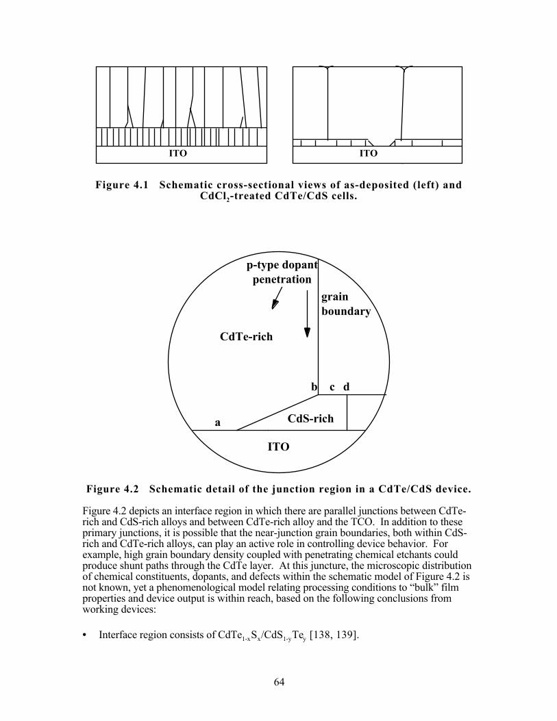
64
ITO ITO
Figure 4.1 Schematic cross-sectional views of as-deposited (left) andCdCl2-treated CdTe/CdS cells.
CdTe-rich
ITO
CdS-richa
b c d
p-type dopantpenetration
grainboundary
Figure 4.2 Schematic detail of the junction region in a CdTe/CdS device.
Figure 4.2 depicts an interface region in which there are parallel junctions between CdTe-rich and CdS-rich alloys and between CdTe-rich alloy and the TCO. In addition to theseprimary junctions, it is possible that the near-junction grain boundaries, both within CdS-rich and CdTe-rich alloys, can play an active role in controlling device behavior. Forexample, high grain boundary density coupled with penetrating chemical etchants couldproduce shunt paths through the CdTe layer. At this juncture, the microscopic distributionof chemical constituents, dopants, and defects within the schematic model of Figure 4.2 isnot known, yet a phenomenological model relating processing conditions to “bulk” filmproperties and device output is within reach, based on the following conclusions fromworking devices:
• Interface region consists of CdTe1-xSx/CdS1-yTey [138, 139].
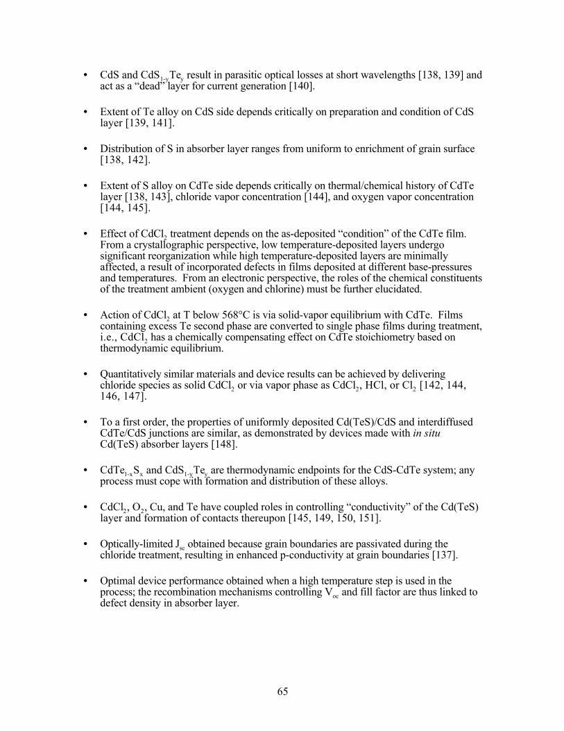
65
• CdS and CdS1-yTey result in parasitic optical losses at short wavelengths [138, 139] andact as a “dead” layer for current generation [140].
• Extent of Te alloy on CdS side depends critically on preparation and condition of CdSlayer [139, 141].
• Distribution of S in absorber layer ranges from uniform to enrichment of grain surface[138, 142].
• Extent of S alloy on CdTe side depends critically on thermal/chemical history of CdTelayer [138, 143], chloride vapor concentration [144], and oxygen vapor concentration[144, 145].
• Effect of CdCl2 treatment depends on the as-deposited “condition” of the CdTe film.From a crystallographic perspective, low temperature-deposited layers undergosignificant reorganization while high temperature-deposited layers are minimallyaffected, a result of incorporated defects in films deposited at different base-pressuresand temperatures. From an electronic perspective, the roles of the chemical constituentsof the treatment ambient (oxygen and chlorine) must be further elucidated.
• Action of CdCl2 at T below 568°C is via solid-vapor equilibrium with CdTe. Filmscontaining excess Te second phase are converted to single phase films during treatment,i.e., CdCl2 has a chemically compensating effect on CdTe stoichiometry based onthermodynamic equilibrium.
• Quantitatively similar materials and device results can be achieved by deliveringchloride species as solid CdCl2 or via vapor phase as CdCl2, HCl, or Cl2 [142, 144,146, 147].
• To a first order, the properties of uniformly deposited Cd(TeS)/CdS and interdiffusedCdTe/CdS junctions are similar, as demonstrated by devices made with in situCd(TeS) absorber layers [148].
• CdTe1-xSx and CdS1-yTey are thermodynamic endpoints for the CdS-CdTe system; anyprocess must cope with formation and distribution of these alloys.
• CdCl2, O2, Cu, and Te have coupled roles in controlling “conductivity” of the Cd(TeS)layer and formation of contacts thereupon [145, 149, 150, 151].
• Optically-limited Jsc obtained because grain boundaries are passivated during thechloride treatment, resulting in enhanced p-conductivity at grain boundaries [137].
• Optimal device performance obtained when a high temperature step is used in theprocess; the recombination mechanisms controlling Voc and fill factor are thus linked todefect density in absorber layer.

66
• Low resistance back-contacts are facilitated by enhanced p-conductivity at the backsurface [152]. Variations in back-contact processing can produce as-yet unexplainedvariations in Voc which may be due to penetration of contacting agents along grainboundaries [153].
4 .2 .2 Critical issues
For the framework to be relevant to the overall goal of developing a successful low-costthin-film photovoltaic module, the research needs to maintain focus upon the critical issues.During Phase I of this contract, research efforts were directed at the critical issues definedbelow for performance, stability, and manufacturability.
For polycrystalline thin-film CdTe/CdS solar cells, the performance-limiting issues arerelated to the fundamental quantities that determine built-in voltage, recombination, carriertransport, and Ohmic contact. With the present device structure, the critical performance-limiting issue is control of the CdS layer. To maximize the current density output, the CdSmust be as thin as possible without producing junctions between the CdTe and the TCO.This is because the junction between CdTe and the available TCO materials exhibits a largerdiode current than the junctions with CdS. Developments in TCO technology mayeventually allow elimination of the CdS layer entirely, which will shift the focus towardsthe electronic properties of the CdTe layer. Another option for increasing the currentdensity is to utilize photocarriers generated within the CdS layer; for these carriers to becollected the field must cross the interface, making the device susceptible to interfacerecombination.
The critical stability-controlling issues, while not fully definable, will relate to theinfinitesimal nature of the CdS layer and to the robustness of the dopants and contacts.Minimization of CdS thickness to maximize current density may affect the sensitivity of thecell to thermal or electrical bias stresses, making the long-term stability of cells with ultra-thin CdS a critical issue. In addition, various dopant materials and chemical species areintroduced into the cell structure at various phases of processing; their interaction andmodification under stress conditions and over long periods of time must be fullyunderstood in the context of stability.
The critical issue of manufacturability of CdTe/CdS thin-film devices is defined by thebalance between maximum performance achievable at minimum processing and materialscost. Fully understanding and solving the critical issues of performance and stability willnaturally lead to innovative options for low-cost processing. As a guiding philosophy,near-atmospheric vapor processes were sought to replace liquid chemical processes.
4.3 CdS-CdTe Interaction
4 .3 .1 Approach and Techniques
4 .3 .1 .1 Film Deposition
The goals of identifying, quantifying and controlling the interaction between CdS and CdTelayers in thin-film device structures were achieved by:
1. Utilizing a baseline fabrication process for CdTe/CdS cells;

67
2. Establishing a measurement protocol for quantifying CdS properties and content inwindow and absorber layers;
3. Measuring CdS content in absorber layer before and after post-deposition treatments;4. Correlating photovoltaic output of devices with resultant CdS window layer thickness;5. Using (2) and (3) above to evaluate cells made with CdTe1-xSx alloy absorber layers and
with modified post-deposition treatments.
The baseline process is defined below:
1. Physical vapor deposition of CdS film onto ~200 nm ITO (20Ω/sq)/Corning 7059glass.
2. CdCl2 treatment @ 420°C for 10-20 min [141].3. Physical vapor deposition of ~5 µm thick CdTe film onto treated CdS at T ~ 250°C.4. CdCl2 vapor treatment @ 420°C for 15 min in air [154].5. Etch to produce Te excess.6. Deposit Cu film with in situ heat treatment @ 200°C for 30 min [152].7. Etch excess Cu away with bromine-methanol.8. Apply carbon ink conductor, dry for 4-6 hours.
This baseline fabrication process allows the effects of individual processing steps to bealtered and evaluated independent of other steps; for example, the copper doping step isseparated from the application of the current-carrying conductor. New to the process inthis contract year is performing the copper diffusion step within the copper depositionreactor.
Nine 1” x 1” samples, including one with an embedded thermocouple, are coated in eachphysical vapor deposition. The arrangement utilized within the bell jar to deposit the alloyabsorber layers is shown in Figure 4.3. Deposition is obtained by dissociative evaporationof the CdTe and CdS powders within the effusion sources and free molecular flow fromsource to substrate in the vacuum at a base pressure of ~10-6 Torr :
CdTes ---> Cdv + 1/2(Te2)v (4.1)
CdSs ---> Cdv + 1/2(S2)v. (4.2)
The effusion rate (ro) from the sources is a function of the pressure drop across the effusionorifice (P1-P2) and the effective gas phase molecular weight (Meff):
ro ~ (Meff/RT)0.5(P1-P2), (4.3)
where P1 = gas pressure at orifice.
The incident flux (ri) at the substrate, y units away, is a function of the angle (θ) from thecenter line:
ri ~ (rocos3/2θ)/y2 (4.4)
At the substrate, the deposition rate depends on the component sticking coefficients andreaction rates. The composition of the deposit depends on the ratio of the effusion fluxes

68
and relative sticking coefficients (δCd, δTe,δS). For typical deposition temperatures used tomake CdTe1-xSx [155]:
δS < δCd < δTe. (4.5)
Radiative Ta Heater
QCM
Shutter (closed)
y = 20 cm
Tsub = 250o C9 - 1"x 1"substrates
EffusionSources
CdT
e
CdS
Base Pressure =1 x 10⁻⁵ Torr
θ
Figure 4.3 Schematic cross-section view of physical deposition systemfor CdTe1-xS x absorber layers.
CdTe1-xSx films were deposited as uniform layers and as stepped layers to investigate therate of CdS consumption for different quantities and distributions of S within the absorberlayer. The stepped layers were formed by depositing a ~1 µm uniform layer at the CdSinterface and then shutting off the CdS source.
4 .3 .1 .2 Film Characterization - CdS
Optical absorption and step profilometry measurements were used to determine initial CdSfilm thickness. Figure 4.4 shows the transmission, normalized for reflection, obtainedfrom CdTe/ITO/7059 samples deposited during the present contract year. For thestructures employed in this work, at constant ITO thickness, the CdS thickness isdetermined using:
d (cm) = 8 x 10⁻⁶ ln T(400nm) - 0.43. (4.6)

69
0
0.2
0.4
0.6
0.8
1
400 450 500 550 600 650 700T/
(1-R
)Wavelength (nm)
25 nm
50 nm
100 nm
300 nm
Figure 4.4 Measured optical transmission, normalized for reflection ofCdS/ITO/7059 (samples from depositions 12148, 12157, 12176,
and 12143).A key concern raised in 1996, the drop in open circuit voltage experienced as CdSthickness, is reduced. The existence of localized and somewhat uniformly distributeddiscontinuities in the CdS layer after cell fabrication offers an explanation of thisphenomenon by allowing for the existence of parallel diodes between CdTe/CdS andCdTe/ITO. The latter junction exhibits a higher diode current, Jo, and will exert a limitinginfluence on Voc depending on the ratio of areas between the two types of junctions.Junctions between the CdTe and TCO could arise due to at least three sources: 1) pinholespresent in as-deposited CdS films; 2) depletion of CdS due to diffusion into CdTe; and 3)breakdown of particulate residues, leaving exposed ITO. Particulates can also create hardshunt paths, reducing Voc from increased shunt conductance. These phenomena aredepicted schematically in Figure 4.5, and the equivalent circuit and circuit equation areshown in Figure 4.6.
Contact
CdTe
CdS
Particulate
Pinhole
TCOGlass
Figure 4.5 Voc-limiting defects attributable to CdS and TCO processing.

70
V
JCdTe/CdS
JCdTe/ITO
JL
= AkT lnqVocJ L
JoCdS(1 - F) + (F)
TCOJo[ ]
Figure 4.6 Equivalent circuit and equation for parallel diodes betweenCdTe/CdS and CdTe/TCO.
To provide data for CdS films of different thicknesses made by different methods, filmsfrom different groups of the NREL National CdTe Team were microscopically surveyedfor pinhole and particulate areal density using the following methodology:
1. Pinhole and Surface Particulate AreaA. Contrast-Enhanced Optical MicroscopyB. Survey > 1 cm2 Area in 1 mm Wide StripsC. Count Pinholes According to SizeD. Calculate Fractional Area (F)
2. Surface Particulate HeightA. High Magnification Microscopy (~800X)B. Difference in Focus Plane from Basal Film to Tip of Particulate
3. CdS Film ThicknessA. Optical Transmission and ReflectionB. Measure in High Absorption Band (λ = 400 nm)C. Correct for TCO AbsorptionD. Calculate d(CdS) using α(400 nm)
Enhanced contrast optical microscopy was used for pinhole detection on thin CdS, madepossible in transmission mode by rejection of unwanted E < Eg(CdS) light using abandpass filter as shown in Figure 4.7. The optical transmission properties of both filmand filter are shown in Figure 4.8. Low magnification photographs show the contrastenhancement obtained (Figure 4.9). At higher magnifications pinholes as small as 5 µmdiameter can be detected on CdS films as thin as 50 nm. Tabulation of pinholes found onsurveyed strips allows the pinhole area in as-deposited films to be determined, giving adegree of quality control to the window layer. Data for the IEC and NREL CdTe Teamsamples is shown in Table 4.7 below.

71
Mirror
400nm Bandpass FilterTranslational Stage
Objective Lens
Monitor
Printer
Sample
Camera
White Light Source
Video
Video
Figure 4.7 Optical arrangement used to survey CdS films.
0
0 . 2
0 . 4
0 . 6
0 . 8
1
400 500 600 700 800 900
CdS T/(1-R)Filter T/(1-R) Norm.
Tra
nsm
issi
on
Wavelength (nm)
Figure 4.8 Optical transmission of CdS film and Corion 400 nmbandpass filter.

72
Unfiltered 80 X With 400 nm Bandpass FilterFigure 4.9 Optical micrographs of pinholes in PVD CdS film
120 nm thick.
Table 4.7 Results of CdS film pinhole and surface particulate survey.Column definitions are as follows: TCO# = run #; d(CdS) = Thickness;Area h = area of pinholes in survey region; Fh = fractional area of pinholes;Area p = area of particulates in survey region; Fp = fractional area ofparticulates; Fh+Fp = sum of pinhole and particulate fractional areas.
Group Sample ID Superstrate TCO # CdS d(CdS)
Areah
Fh Areap
Fp Fp+Fh
Method (nm) (cm2) (cm2)MRG 707 ITO/7059 92024 Sputter 225 5E-06 5E-06 3E-05 3E-05 3E-05MRG 707 ITO/7059 92024 Sputter 225 1E-05 1E-05 5E-05 5E-05 7E-05MRG 2080 ITO/7059 92024 Sputter 150 4E-06 4E-06 4E-05 4E-05 4E-05MRG 2080 ITO/7059 92024 Sputter 150 9E-06 9E-06 2E-05 2E-05 3E-05MRG 1080 ITO/7059 92024 Sputter 50 2E-05 2E-05 3E-05 3E-05 5E-05UTol CS 105 7059 no O2 N/A Sputter 300 8E-05 8E-05 2E-04 2E-04 2E-04UTol UB 3 7059 no O2 N/A Sputter 90 4E-06 4E-06 2E-04 2E-04 2E-04UTol CS 94 LOF no O2 Tec20 Sputter 50 2E-05 2E-05 2E-04 2E-04 2E-04UTol CS 95 LOF + O2 Tec20 Sputter 50 0E+00 0 2E-04 2E-04 2E-04UTol CD 92 LOF + O2 Tec15 Sputter 50 2E-05 2E-05 1E-04 1E-04 1E-04NREL A 208 SnO2/7059 CBD 106 1E-05 1E-05 5E-05 4E-05 5E-05NREL A 207 SnO2/7059 CBD 40 1E-05 1E-05 6E-05 6E-05 7E-05CSM 3-12 SnO2/7059 Elec ~120 5E-05 3E-05 2E-06 1E-06 3E-05CSM 28-11 SnO2/7059 Elec ~120 2E-05 5E-06 2E-06 6E-07 6E-06IEC 12094.11 ITO/7059 92144 PVD 200 5E-06 5E-06 4E-06 4E-06 9E-06IEC 12045.11 ITO/7059 91949 PVD 120 2E-05 2E-05 7E-06 7E-06 2E-05IEC 12038.11 ITO/7059 91950 PVD 100 2E-05 2E-05 4E-06 4E-06 2E-05IEC 12089.11 ITO/7059 92083 PVD 70 5E-05 5E-05 4E-06 4E-06 5E-05IEC 12090.11 ITO/7059 92083 PVD 25 N/A N/A 4E-06 4E-06 “4E-06”
Before microscopic examination, the pieces were ultrasonically rinsed in methanol anddried under forced argon. Films were surveyed in transmission mode with a bandpass

73
filter to enhance contrast. Particulates were included in the survey since they can lead toshunt paths as pinholes in CdS (formed via reaction during treatments) or spikes throughthe CdTe layer. Their vertical dimension (normal to film plane) was measured as: 5-10 µmon CDB and Sputtered films and < 5 µm on PVD films.
For the MRG and IEC cases, the samples were on 7059/ITO, with the ITO sputtered atIEC. The 70 and 25 nm cases were witness pieces to the set #2 samples. The NRELsamples were witness pieces to those employed for cell fabrication in set #1. TheUniversity of Toledo samples were on different superstrates and sputtering conditions. TheCSM samples were deposited at different pH and temperature conditions.
For the CSM samples, the number of surface particulates was very low (~1 per sample).The entire surface was surveyed (in 1 mm from the edges to discount edge, cutting, andtweezer effects). The sample 3-12 was deposited at pH = 2.65 and T = 80°C and had anorder of magnitude greater density of pinhole area than sample 28-11, deposited at pH =3.0 and T = 90°C. Sample 3-12 had over 30 pinholes, while 28-11 had only 9.
For the IEC samples made by PVD, the 25 Å case exhibited low optical contrast, makingpinhole assessment difficult. For the other PVD samples, pinhole area increased withdecreasing CdS thickness.
For the NREL CBD samples, the pinhole area was low but the particulate was high. EDSexamination of the particulates revealed the presence of Sn, Al, Si, and Cl.
For all of the samples examined, the following short summary is given:
1. PVD: inverse correlation between pinhole area and CdS thickness; constant particulatearea.
2. CBD: constant fractional pinhole and particulate area.
3. RF Sputtered: no trend in pinholes, constant particulate.
4. For PVD cells, pinhole density accounts for Voc falloff with ITO; need more cell data onJo of CdTe/SnO2 cells to draw a firm conclusion.
The effect of the summed areal fractions on Voc is shown in Table 4.8, using A-factors, JL,and Jo for the CdTe/CdS and CdTe/ITO junctions.
Table 4.8 Estimated drop in Voc versus F for CdTe/CdS/ITO.
F (holes)(%)
Voc
(mV)∆Voc
(mV)0 840 0
0.001 830 100.01 786 540.1 687 1531 570 270
100 330 510
In the table, a fractional pinhole area of 1E-04 would produce a 60-70 mV drop in Voc for aCdTe/CdS junction having Voc = ~840 mV. Surveying every square cm of every sample is

74
not practical, but monitoring control or witness pieces can be a valuable tool for assessingperformance of ultra-thin CdS before using it in a cell structure. In the future, we hope tocombine CdS film transmission mapping with high resolution OBIC mapping to correlatethe extent and uniformity of localized CdS defects with voltage output of the devices.
4 .3 .1 .3 Film Characterization - CdTe and CdTe1-xS x
CdTe and CdTe1-xSx film thicknesses were determined by mass gain of the superstratesafter deposition. For uniform CdTe1-xSx alloy films, the as-deposited composition wasdetermined by energy dispersive x-ray spectroscopy (EDS), and wide-angle θ/2θ scanningx-ray diffraction (XRD) and lattice parameter reduction [138]. Selected samples wereanalyzed in cross-section by transmission electron microscopy (TEM).
In devices, the CdS loss incurred during post-CdTe treatments was determined bymeasurement of the quantum efficiency from 400 to 450 nm, which is found to be limitedby parasitic optical absorption in the CdS layer. In the device structure, the CdS layeressentially acts as a thickness-dependent optical filter for the high absorption region (E >Eg), since carriers which are generated in the CdS layer are not collected. For the presentdevices this assumption has been confirmed by selectively etching away the Te-rich layersand comparing the 400 nm to 450 nm optical transmission to the quantum efficiency asshown in Figure 4.10. In the case shown, the values at 400 nm differ by less than 2relative percent, which translates to an error in CdS thickness of ±5 nm. For routine usewith small area cells, care must be taken to minimize errors in the cell area used to computethe quantum efficiency to avoid larger deviations.
0
0.1
0.2
0.3
0.4
0.5
0.6
400 420 440 460 480 500
QE
and
Tra
nsm
issi
on
Wavelength (nm)
Figure 4.10 Short wavelength quantum efficiency of CdTe/CdS thin-filmdevice (solid line) compared to CdS transmission (dotted line) after
removal of Te-rich layers (sample 40992.31/12127.31).
The accumulation of CdS within the absorber layer after thermal and chemical treatmentswas determined by x-ray diffraction line profile analysis. XRD techniques yield latticeparameter variations in the layers producing the diffracted signal, which for the CdTe (511)or (531) peaks, is restricted to a depth of 3 µm. For glancing XRD techniques, in whichthe primary beam angle is fixed, the depth sampled is restricted to thinner surface layers.Similarly, EDS measurements give compositional data for ~0.5 - 1 µm from the exposed“back” surface. Obtaining compositional data near the junction region by these methodsthus requires thinner absorber layers; in this work, access to the junction region wasfacilitated by etching the absorber layer in dichromate solution to a thickness of ~ 2 µm. In

75
devices, the long-wavelength fall-off of the quantum efficiency provides a measure of thebandgap, hence composition, in the junction region.
X-ray diffraction measurements of the CdTe1-xSx absorber layer were made with Cu-kα x-rays using a Philips/Norelco θ-2θ scanning diffractometer (Bragg-Brentano parafocusinggeometry) fitted with a diffracted-beam monochrometer. Data was acquired by step-scanning: in constant time mode for broad angular scans and constant count mode fordetailed peak profile acquisition. This focusing geometry, while sampling crystalpopulations aligned with the substrate, is not ideal for examining ultra-thin CdS orinterfacial layers because of the very low diffracting volume presented by the CdS film orinterface at the high angles needed for good angular resolution. For this, an effort wasinitiated to evaluate glancing incidence diffractometry (hybrid Seehman-Bohlinparafocusing geometry) of CdS/CdTe structures in which the CdTe was chemically thinnedto < 0.5 µm (samples prepared by Andreas Fischer and Al Compaan at the University ofToledo).
The limitations of the measurements and analyses are as follows. The x-ray samplingdepth, defined as the film thickness contributing to detectable diffracted x-ray signal, is afunction of the Bragg angle and varies from ~1 µm at 2θ = 20° to ~4 µm at 2θ = 80°.Thus, devices with thick CdTe, > 3 µm, had to be thinned to access the interfacial region.Variability in CdTe/CdS sample area makes comparative intensities useless, so these havebeen avoided in the results section. A sample broad θ-2θ scan and corresponding Nelson-Riley-Sinclair-Taylor (NRST) fit is presented in Figure 4.11 and Figure 4.12. The error inthe extrapolated “precision” lattice parameter, +/- 0.001 Å, is related to the step size andSNR of the peaks, which lead to errors in d-spacing. This translates to an absolutecompositional error of +/- 0.3%. On narrow angle scans, detection of an alloy componentdepends on thickness and attenuation. For the diffraction system used, a SNR = 1 isobtained for the (511) peak of a CdTe film 20-30 nm thick.
On all data, standard spectral reductions to remove α2 components, smooth data, andcalculate lattice parameter were performed using software developed at IEC by BrianMcCandless and Garth Jensen in 1996. Quantification of x-ray diffraction line profiles wasachieved by Fourier deconvolution of the diffractometer instrument function from themeasured profiles, using an annealed CdTe powder standard for the desired (hkl)reflection. The resulting profiles consisted of an angular distribution of intensities whichwere numerically integrated with respect to composition, yielding a net CdS content inCdTe1-xSx. The specific reduction steps used to determine film orientation, “bulk” absorberlayer CdTe1-xSx composition, and to infer compositional distribution are summarizedbelow.
CdTe 1-x S x Film Orientation and Bulk CdTe 1-x S x Composition
• Acquire broad 2θ scan (20-90°, step = 0.05°, count for 2 or 4 seconds per step).• Remove α2 components and smooth (floating 3-point binomial).• Index pattern with ICDD standard using most intense component of (hkl) peaks.• Compute orientation parameter, p(111), by method of Harris [156] for fiber texture
analysis. In this study, p(111) was computed using first 7 (hkl) peaks of the randompattern. Thus, p(111) = 7 indicates a perfectly (111) oriented film, p(111) = 1 indicatesrandom orientation, and p(111) < 1 indicates dominance of a different orientation.
• Compute precision lattice parameter using Nelson-Riley-Sinclair-Taylor reduction [157,158].

76
• Compute CdTe1-xSx composition corresponding to lattice parameter using Vegardrelation for the CdS-CdTe system: x = 1.508 x (6.481 - ao) [138].
CdTe 1-x S x Compositional Distribution
• Acquire narrow 2θ scan (step = 0.01°, constant count mode = 1000 counts per step) ofhigh angle peak such as (511).
• Remove α2 components and smooth (floating 3-point binomial).• Normalize profile to most intense component.• Fit CdTe side of profile to Pearson VII to determine HWHM [159]. For high angle
peaks, such as CdTe (511), the presence of asymmetric components on high-angle sideis interpreted as CdTe1-xSx alloy [160] having composition given by: x = 1.508 x(6.481 - ao) [138].
• Deconvolve instrument function [161]• Estimate integrated CdS content.• Determine equivalent CdS thickness.• Compare to change in CdS thickness estimated from changes in the optical transmission
of the CdS layer inferred from the device quantum efficiency at 400 nm as describedabove.
CdS 1-y Te y Compositional Distribution
• Acquire narrow 2θ scan with fixed incident beam angle.• Remove α2 components and smooth (floating 3-point binomial).

77
No. 2 theta cnts d (A)
1 23.8 1186.73.735532 26.55 550.0843.354523 39.3 6065.572.290644 46.45 2001.391.953335 47.85 113.0261.899396 51.7 369.8491.766637 54.6 82.79561.679458 56.85 80.23951.618219 62.45 254.0431.48588
10 65.85 121.4811.4171511 71.25 336.7761.3224212 76.35 239.0031.2462813 78.6 47.64021.2161414 84.55 307.1441.1450815 89.4 173.3351.09509
1000
800
600
400
200
0
Inte
nsit
y (A
U)
80604020
2-Theta (deg)
1
2
3 4
5
6
7 8
9
10
11
12
13
14
15
SCI5EB.TXT
alpha2 stripped, 3 pt. binomial smoothing, step=0.05°, 4 sec.
Figure 4.11 Data Example 1 - Broad scan and peak table - SCI 005 afterthinning to 2 µm.

78
peak_numTwoTheta NRST H K L a
1 23.8 4.6267 1 1 1 6.470112 39.3 2.6118 2 2 0 6.478893 46.45 2.112443 1 1 6.478454 56.85 1.591884 0 0 6.472835 62.45 1.376213 3 1 6.47686 71.25 1.098484 2 2 6.478517 76.35 0.9637095 1 1 6.475848 84.55 0.7779484 4 0 6.477529 89.4 0.6829435 3 1 6.47864
6.48
6.46
6.44
6.42
6.40
a (A
)
543210
NRST value
12
10
8
6
4
2
0
x of
CdT
e1-x
S x (
%)
aCdTe
6.4
6.3
6.2
6.1
6.0
5.9
a (A
)
543210
NRST value
100
80
60
40
20
0
x of
CdT
e1-x
S x (
%)
aβ-CdS
aCdTe
SCI 005 - Extrapolated Lattice Parameter = 6.479 Å (x ~ 0.3%)
Figure 4.12 Data Example 2 - NRST reduction of CdTe1-xS x peaks ofExample 1.
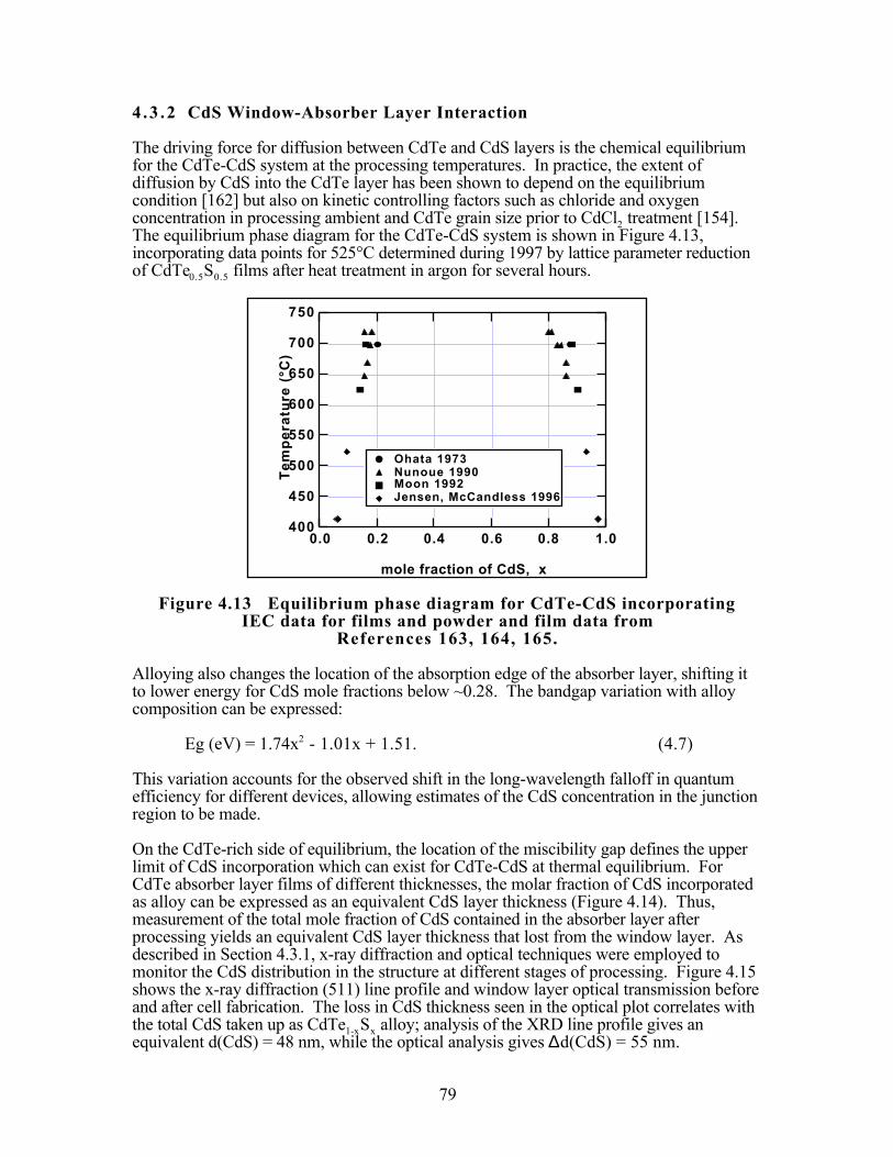
79
4 .3 .2 CdS Window-Absorber Layer Interaction
The driving force for diffusion between CdTe and CdS layers is the chemical equilibriumfor the CdTe-CdS system at the processing temperatures. In practice, the extent ofdiffusion by CdS into the CdTe layer has been shown to depend on the equilibriumcondition [162] but also on kinetic controlling factors such as chloride and oxygenconcentration in processing ambient and CdTe grain size prior to CdCl2 treatment [154].The equilibrium phase diagram for the CdTe-CdS system is shown in Figure 4.13,incorporating data points for 525°C determined during 1997 by lattice parameter reductionof CdTe0.5S0.5 films after heat treatment in argon for several hours.
750
700
650
600
550
500
450
400
Tem
pera
ture
(°C
)
1.00.80.60.40.20.0
mole fraction of CdS, x
Ohata 1973 Nunoue 1990 Moon 1992 Jensen, McCandless 1996
Figure 4.13 Equilibrium phase diagram for CdTe-CdS incorporatingIEC data for films and powder and film data from
References 163, 164, 165.
Alloying also changes the location of the absorption edge of the absorber layer, shifting itto lower energy for CdS mole fractions below ~0.28. The bandgap variation with alloycomposition can be expressed:
Eg (eV) = 1.74x2 - 1.01x + 1.51. (4.7)
This variation accounts for the observed shift in the long-wavelength falloff in quantumefficiency for different devices, allowing estimates of the CdS concentration in the junctionregion to be made.
On the CdTe-rich side of equilibrium, the location of the miscibility gap defines the upperlimit of CdS incorporation which can exist for CdTe-CdS at thermal equilibrium. ForCdTe absorber layer films of different thicknesses, the molar fraction of CdS incorporatedas alloy can be expressed as an equivalent CdS layer thickness (Figure 4.14). Thus,measurement of the total mole fraction of CdS contained in the absorber layer afterprocessing yields an equivalent CdS layer thickness that lost from the window layer. Asdescribed in Section 4.3.1, x-ray diffraction and optical techniques were employed tomonitor the CdS distribution in the structure at different stages of processing. Figure 4.15shows the x-ray diffraction (511) line profile and window layer optical transmission beforeand after cell fabrication. The loss in CdS thickness seen in the optical plot correlates withthe total CdS taken up as CdTe1-xSx alloy; analysis of the XRD line profile gives anequivalent d(CdS) = 48 nm, while the optical analysis gives ∆d(CdS) = 55 nm.

80
0
5 0
100
150
200
0 0 .01 0 .02 0 .03 0 .04 0 .05 0 .06
d(Cd
S)eq
(n
m)
mole fraction of CdS, x
10 um 5 um
2 um
1 um
Figure 4.14 Equivalent CdS thickness versus molar fraction of CdS inCdTe1-xS x for different total alloy film thicknesses. Single crystal
densities were assumed in this approximation.
1.0
0.8
0.6
0.4
0.2
0.0
Norm
aliz
ed Inte
nsi
ty
76.876.476.0
2θ (deg)
0
0.2
0.4
0.6
0.8
1
4 0 0 5 0 0 6 0 0 7 0 0 8 0 0 9 0 0
QE/
(1-R
) an
d T/
(1-R
)
Wavelength (nm)
Figure 4.15 X-ray diffraction line profile of CdTe1-xS x (511) after deviceprocessing (left) and optical transmission of CdS before processing
and device quantum efficiency (right).
These measurement techniques were used to analyze samples fabricated by the members ofthe NREL CdTe Team. Devices were made with “thick” and “thin” CdS on TCO/glasssuperstrates provided by Chris Ferekides of the University of South Florida. The sampleswere selected from a larger group to give two CdS thicknesses: ~50 nm and ~130 nm. TheJ-V and QE characteristics of the devices were measured and reported by Jim Sites ofColorado State University. XRD analysis was performed at the Institute of EnergyConversion and selected samples were forwarded to the National Renewable EnergyLaboratory for SIMS analysis, which was completed in April, 1997. The groupsrepresented on the national team which participated in this and related XRD analyses arelisted, with abbreviations, below:

81
Colorado School of Mines CSMGolden Photon, Incorporated GPIInstitute of Energy Conversion IECNational Renewable Energy Laboratory NRELSolar Cells, Incorporated SCIUniversity of South Florida USFUniversity of Toledo UT
The samples used in the study were from CdS Team "Set #1" and were fabricated onSnO2/7059 superstrates provided by Chris Ferekides at the University of South Florida.Each participating team member was asked to prepare devices with "thick" and "thin" CdSusing their standard process. Given that fabrication processes are constantly evolving, thefindings herein apply to CdTe/CdS processed in the early 1996 period. Golden Photon didnot participate in this particular study, but their standard material was provided privately forXRD analysis and constitutes a unique data set. The deposition processes and as-receivedfilm thicknesses represented in this study are listed in Table 4.9. On the CSM, IEC, andUT samples, sufficient CdTe area was available for performing XRD measurements; forthe NREL, SCI, and USF samples, the back contacts were removed to provide sufficientexposed CdTe area for XRD analysis.
Table 4.9 Participating groups, deposition processes, and approximatefilm thicknesses for Set #1 samples used in x-ray diffraction study: CSS =close-space sublimation, ED = electrodeposition, EVD = elemental vapordeposition, PVD = physical vapor deposition, RFSD = rf sputterdeposition.
Group CdS DepositionMethod
CdS InitialThicknesses
(nm)
CdTe DepositionMethod
CdTeThickness
(µm)CSM CBD 70 and 150 ED 2IEC PVD 50 and 110 PVD 4-5
NREL CBD 90 and 140 CSS 7-8SCI CSS 60, 100, 150 EVD 4-5USF CBD 75 and 105 CSS 7-8UT RFSD 40 and 140 SD 2
Table 4.10 summarizes the methods used to reduce the CdTe layer thickness and the XRDmeasurements performed on each sample. Final thicknesses were checked byprofilometry.

82
Table 4.10 Summary of sample identification, preparation and XRDmeasurements performed.
Group/Sample # di (CdS)nm
d(CdTe)µm
XRDBroad
Scan(511)
ThinningTechnique
XRDBroad
Scan(511)
CSM 655 70 2 √ √ none n/a n/aCSM 651 150 2 √ √ none n/a n/a
IEC 913.13 50 4 - 5 √ √ dichromate √ √IEC 913.12 110 4 - 5 √ √ dichromate √ √NREL A85 90 7 - 8 √ √ dichromate √ √NREL A84 140 7 - 8 √ √ dichromate √ √
SCI 001 60 4 - 5 √ - dichromate - √SCI 002 60 4 - 5 √ √ bromine-methanol √ √SCI 004 100 4 - 5 √ √ bromine-methanol √ √SCI 005 150 4 - 5 √ - dichromate - √SCI 006 150 4 - 5 √ √ bromine-methanol √ √
USF 8-14A-14 75 7 - 8 √ √ mech + dichromate √ √USF 8-14A-16 105 7 - 8 √ √ mech + dichromate √ √
UT 306 40 2 √ √ none n/a n/aUT 304 140 2 √ √ none n/a n/a
4 .3 .2 .1 CdTe1-xS x Film Orientation and Bulk CdTe1-xS x Composition
The orientation parameter, lattice parameter and value of x in CdTe1-xSx for samples beforeand after thinning to ~2 µm are shown in Table 4.11. To compare all samples at equivalentCdTe thickness, refer to the “Thinned” column.
Table 4.11 Orientation and CdTe1-xSx composition from broad XRDscans before (Initial) and after thinning (Thinned) CdTe layer to 2 µm.
Sample di (CdS)
(nm)
OrientationParameter
p(111)Initial Thinned
LatticeParameter
(Å) +/- 0.001 ÅInitial Thinned
x inCdTe1-xSx
(%) +/- 0.3%Initial Thinned
CSM 655 70 n/a 0.1 n/a 6.476 n/a 0.7CSM 651 150 n/a 0.3 n/a 6.470 n/a 1.6
IEC 913.13 50 0.7 0.7 6.479 6.478 0.3 0.4IEC 913.12 110 0.7 0.8 6.479 6.478 0.3 0.4NREL A 85 90 0.5 1.0 6.479 6.479 0.3 0.3NREL A84 140 0.7 0.8 6.480 6.480 0.2 0.2
SCI 002 60 0.4 0.3 6.477 6.480 0.6 0.2SCI 004 100 0.3 0.3 6.479 6.479 0.3 0.3SCI 005 150 0.3 0.2 6.478 6.479 0.4 0.3USF 14 75 1.2 1.6 6.480 6.476 0.2 0.7USF 16 105 1.1 1.3 6.478 6.480 0.4 0.2UT 306 40 n/a 0.3 n/a 6.475 n/a 0.9UT 304 140 n/a 0.5 n/a 6.477 n/a 0.6
In all but the USF films, p(111) is less than 1, indicating preferential orientation of adifferent plane, which was the (220) in all cases. The USF films exhibited p(111) slightly
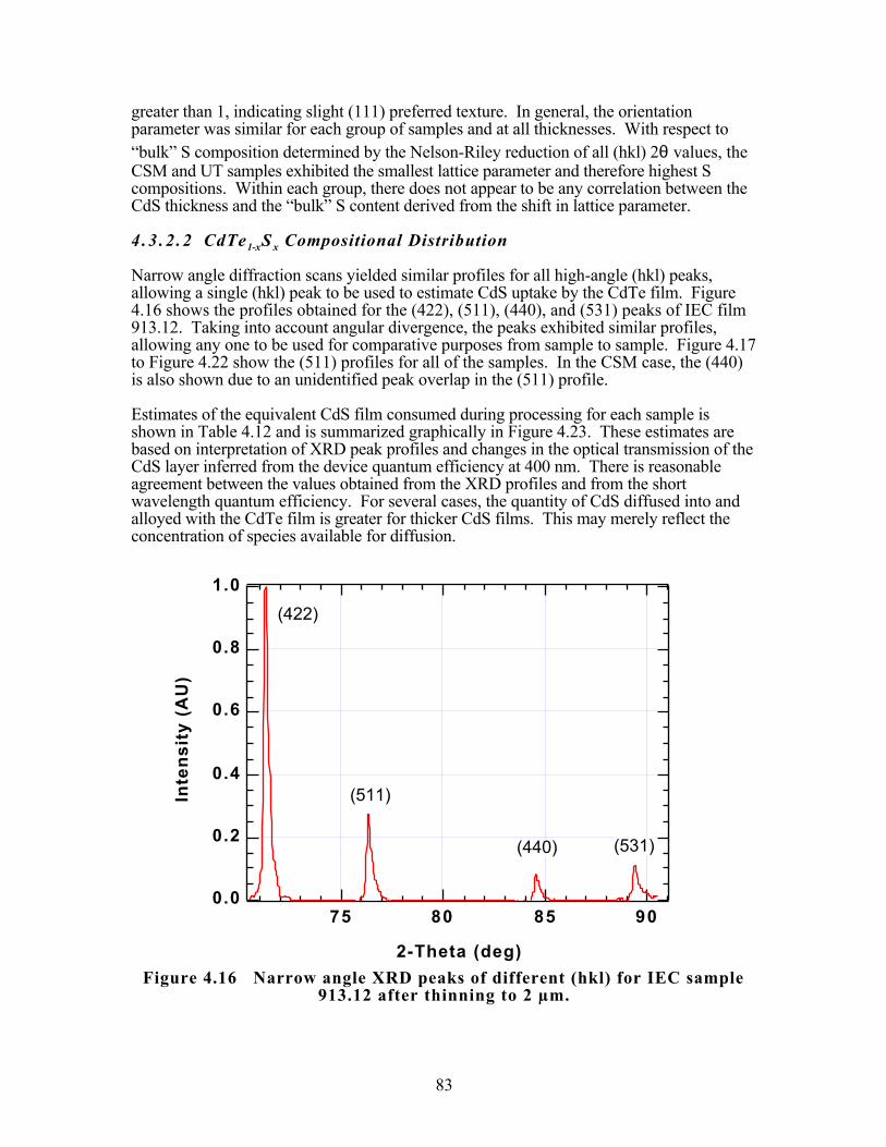
83
greater than 1, indicating slight (111) preferred texture. In general, the orientationparameter was similar for each group of samples and at all thicknesses. With respect to“bulk” S composition determined by the Nelson-Riley reduction of all (hkl) 2θ values, theCSM and UT samples exhibited the smallest lattice parameter and therefore highest Scompositions. Within each group, there does not appear to be any correlation between theCdS thickness and the “bulk” S content derived from the shift in lattice parameter.
4 .3 .2 .2 CdTe1-xS x Compositional Distribution
Narrow angle diffraction scans yielded similar profiles for all high-angle (hkl) peaks,allowing a single (hkl) peak to be used to estimate CdS uptake by the CdTe film. Figure4.16 shows the profiles obtained for the (422), (511), (440), and (531) peaks of IEC film913.12. Taking into account angular divergence, the peaks exhibited similar profiles,allowing any one to be used for comparative purposes from sample to sample. Figure 4.17to Figure 4.22 show the (511) profiles for all of the samples. In the CSM case, the (440)is also shown due to an unidentified peak overlap in the (511) profile.
Estimates of the equivalent CdS film consumed during processing for each sample isshown in Table 4.12 and is summarized graphically in Figure 4.23. These estimates arebased on interpretation of XRD peak profiles and changes in the optical transmission of theCdS layer inferred from the device quantum efficiency at 400 nm. There is reasonableagreement between the values obtained from the XRD profiles and from the shortwavelength quantum efficiency. For several cases, the quantity of CdS diffused into andalloyed with the CdTe film is greater for thicker CdS films. This may merely reflect theconcentration of species available for diffusion.
1.0
0.8
0.6
0.4
0.2
0.0
Inte
nsit
y (A
U)
90858075
2-Theta (deg)
(531)(440)
(511)
(422)
Figure 4.16 Narrow angle XRD peaks of different (hkl) for IEC sample913.12 after thinning to 2 µm.

84
1.0
0.8
0.6
0.4
0.2
0.0
Inte
nsit
y (A
U)
77.477.277.076.876.676.476.276.0
2-Theta (deg)
1500 A CdS
700 A CdS
1.0
0.8
0.6
0.4
0.2
0.0
Inte
nsit
y (A
U)
85.485.285.084.884.684.484.284.0
2-Theta (deg)
1500 A CdS
700 A CdS
Figure 4.17 Narrow angle (511) (top) and (440) (bottom) XRD peakprofiles for CSM samples with different CdS thickness.

85
1.0
0.8
0.6
0.4
0.2
0.0
Inte
nsit
y (A
U)
77.477.277.076.876.676.476.276.0
2-Theta (deg)
1100 A CdS
500 A CdS
Figure 4.18 Narrow angle (511) XRD peak profiles for IEC samples withdifferent CdS thickness after thinning the CdTe layer to ~2 µm.
1.0
0.8
0.6
0.4
0.2
0.0
Inte
nsit
y (A
U)
77.477.277.076.876.676.476.276.0
2-Theta (deg)
900 A CdS
1400 A CdS
Figure 4.19 Narrow angle (511) XRD peak profiles for NREL sampleswith different CdS thickness after thinning the CdTe layer to ~2 µm.
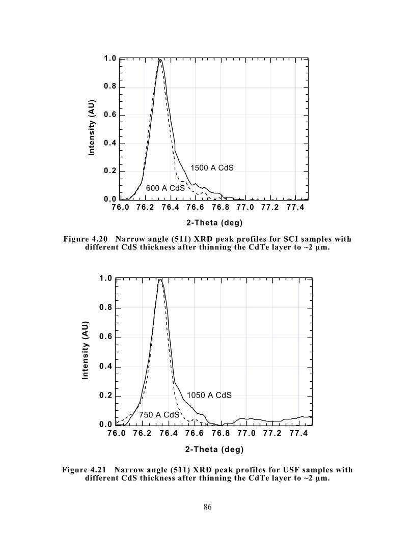
86
1.0
0.8
0.6
0.4
0.2
0.0
Inte
nsit
y (A
U)
77.477.277.076.876.676.476.276.0
2-Theta (deg)
1500 A CdS
600 A CdS
Figure 4.20 Narrow angle (511) XRD peak profiles for SCI samples withdifferent CdS thickness after thinning the CdTe layer to ~2 µm.
1.0
0.8
0.6
0.4
0.2
0.0
Inte
nsit
y (A
U)
77.477.277.076.876.676.476.276.0
2-Theta (deg)
750 A CdS
1050 A CdS
Figure 4.21 Narrow angle (511) XRD peak profiles for USF samples withdifferent CdS thickness after thinning the CdTe layer to ~2 µm.

87
1.0
0.8
0.6
0.4
0.2
0.0
Inte
nsit
y (A
U)
77.477.277.076.876.676.476.276.0
2-Theta (deg)
1400 A CdS
400 A CdS
Figure 4.22 Narrow angle (511) XRD peak profiles for UT sampleswith different CdS thickness.
Table 4.12 Summary of CdTe peak profile and estimate of CdS uptake byCdTe film. The instrument HWHM for CdTe is 0.06°. Determinationsmade by analysis of XRD peak profiles are compared to those made bychange in CdS transmission. Composition of the doublet component isindicated in parentheses in atomic percent.
Sample d(CdS)Initial
(nm)
XRD ProfileShape
HWHM(511)
(deg)
XRDEquivd(CdS)
(nm)
∆d(CdS)from
QE(400nm)
(nm)CSM 655 70 doublet (1.9 %) 0.10 43 41CSM 651 150 doublet (3.5 %) 0.10 47 54
IEC 913.13 50 tail 0.10 32 32IEC 913.12 110 tail 0.10 55 80NREL A85 90 tail 0.09 12 9NREL A84 140 tail 0.09 11 27
SCI 002 60 tail 0.08 27 19SCI 005 150 tail 0.08 30 21USF 14 75 tail 0.07 9 11USF 16 105 tail 0.09 17UT 306 40 tail 0.10 32 22UT 304 140 doublet (2.5 %) 0.10 62 90

88
0
20
40
60
80
100
0 20 40 60 80 100
d(Op
tics-
QE) (
nm)
d(XRD) (nm)∆
∆
Figure 4.23 Change in CdS thickness derived from optical methodscompared to that derived from X-ray diffraction measurements.
In Table 4.12, occurrence of a doublet indicates the presence of a discreet layer at thecomposition given in parentheses. The doublet structure can be seen in the precedingfigures. Modeling of CdS-CdTe diffusion at IEC by Rajesh Venugopal in 1996 for PVDstructures treated at different temperatures, times and CdCl2 concentration showed that suchbimodal distributions cannot be described by simple grain boundary and volume diffusion,even taking into account concentration-dependent diffusion coefficients [166]. To accountfor such distributions in the XRD profile it is necessary to invoke a two- or multiple-stepdiffusion process in which CdS is transported into the CdTe bulk quickly in the initialstages of heat treatment. For the CSM samples, the doublet data was taken from the (440)peak because the (511) peak was not clearly resolved from an unidentified adjacent peak.The presence of a doublet component in the CSM and UT samples correlates with theirhigher “bulk” S compositions shown in Table 4.11. The HWHM values are all verysimilar but are higher for the CSM, IEC, and UT cases. From the equivalent CdSthickness loss estimate, Table 4.12 and Figure 4.23 show that there is reasonableagreement between the XRD and optical methods, showing that more CdS was consumedin the CSM, IEC, and UT processes.
This can be understood by recognizing that the CSM, IEC, and UT structures werefabricated by depositing the CdTe at relatively low temperatures, below 300°C, whichproduces CdTe films with small grains, hence high grain boundary density. The othersamples had CdTe deposited at high temperature, greater than 500°C. All of the sampleshave received a CdCl2 treatment at around 400°C. For CdTe films deposited at lowtemperature, this treatment is known to promote dramatic recrystallization, hence mobilityof the Cd, Te, and S atoms, resulting in enhanced interfacial diffusion. High temperatureduring CdTe growth produces large-grain films with lower defect density, resulting in littleinteraction during the chloride treatment. For the low temperature deposited films, theinteraction can be minimized by performing a high temperature recrystallization before thechloride treatment may offer a means to reduce interdiffusion [167, 168]. The hightemperature approach can be used to enhance performance in cells made by low depositiontemperature processes, but there is still measurable CdS loss that puts a lower limit on thestarting CdS thickness that can be used.

89
For the high temperature processes, limits in Jsc also appear to arise from effects due toCdS1-yTey formation in the window layer. In the quantum efficiency plots for these devices[169], the collection from 450 nm to 600 nm for the NREL and USF cells is lower thanexpected based on a CdS window layer. This effect is likely due to the presence of agraded CdS1-yTey layer that formed during CdTe deposition or during CdCl2 treatment asobserved for PVD cells [141]. More work, as described in the next section, is needed toaddress this problem.
4 .3 .2 .3 CdS 1-yTey Compositional Distribution
It has been previously shown that treatments of the CdS prior to CdTe deposition arenecessary to minimize formation of CdS1-yTey, which reduces the CdS bandgap, adding tothe parasitic absorption of blue-green light [141]. In devices with ultra-thin CdS, thiseffect may be negligible, but as a control issue for squeezing the most out of the device in arepeatable process, the chemical interaction on the CdS side of the device cannot beignored. In analyzing such thin CdS layers, θ-2θ XRD measurements (Bragg-Brentano)yield diffracted CdS signals that are too low to obtain compositional profiles of the highangle peaks needed. Increased signal can be achieved, however, by fixing the incidentbeam at a glancing angle and preparing the specimens for this type of analysis.
For this experiment 2 µm CdTe/0.2 µm CdS structures were sputter-deposited at theUniversity of Toledo on quartz glass. The CdS was not treated prior to CdTe deposition.The CdTe/CdS structures were heat treated with CdCl2 treatment at 320°C and 380°C in air.After heat treatment, the CdTe layer was thinned in bromine-methanol solution. Thethinning procedure yielded a tapered CdTe-CdS interface around the sample edges and amaximum CdTe layer thickness of < 0.5 µm, which was sufficiently thin to permit theglancing incidence technique to be used to sample both CdTe and CdS layerssimultaneously; the resulting thickness profiles are shown in Figure 4.24.
Bragg-Brentano θ /2 θ XRD scans with Cu x-rays only revealed the CdS (002) reflection at2θ = 26.6°. Wide angle diffraction at 4° fixed incident angle revealed CdS (002) and (004)reflections; the (004) peaks were rescanned at smaller step size and slower scan rate toimprove angular resolution and SNR. The Cu kα x-ray penetration depth at 4° is ~450 nmin CdTe, which means that the CdS XRD signal was primarily obtained from the thinnerhalf of the samples. Figure 4.25 shows that both shape and location of the peaks aredifferent for the two films. For the film treated at 320°C, the peak is broadened towardsCdS1-yTey and has a majority component at y = 0. The film treated at 380°C has furtherbroadened and has shifted to y = 2.5% with a tail extending to ~3%. The upper limit ofthese plots, ~ 3%, agrees very well with the compositions determined by Ramanspectroscopy at University of Toledo of the exposed interface. Both measurements directlyconfirm the diffusion of CdTe into CdS during heat treatment with CdCl2. The XRD resultdemonstrates the potential of using glancing incident beam diffraction as a tool forevaluating the interdiffusion on the CdS side of the CdTe/CdS device. An extension of thisapproach will be to further thin the CdTe layers in the sample set and examine themicrocomposition of the window layer.

90
0200400600800
1000
0 5 10 15d(
Tot)
(nm
)Position (mm)
3 2 0
3 8 0
d(CdS)~200 nm
Figure 4.24 Total thickness profile of CdTe/CdS on quartz thinned with0.05% Br2-Ch3OH.
1.0
0.8
0.6
0.4
0.2
0.0
Inte
nsit
y (A
U)
54.854.654.454.254.0
2-Theta (deg)
320°CCdCl2 HT
380°C CdCl2 HT
CdS (004)CdS0 .98Te0 .02
(004)
Figure 4.25 Glancing incidence XRD of CdS (004) on CdCl2-treatedCdTe/CdS/Quartz with CdTe thinned to profile shown in
Figure 4.24; 4° incidence Cu-kα.

91
In summary:
• The techniques of thin-film x-ray diffraction and optics are effective for assessing theinterfacial chemistry of the CdTe-CdS alloy system in solar cells.
• All device structures exhibited measurable alloying between CdS and CdTe in theabsorber layer. Enhanced CdS diffusion was found in devices having CdTe deposited atlow temperature, T < 300°C compared to those having CdTe deposited above 500°C. Thisis understood by noting the dramatic recrystallization that occurs during chloride treatmentof films deposited at low temperatures; films deposited at high temperatures do not undergosignificant recrystallization during chloride treatment and hence absorb less CdS. In thecase of sintered CdTe films, the process is carried out in the presence of chloride whichresults in significant CdS-uptake during CdTe film formation.
• In some of the low temperature-deposited structures the XRD profiles indicate a multi-step mixing process. The profiles of high temperature-deposited CdTe are consistent withgrain boundary and volume diffusion.
• In general, the quantity of S in CdTe1-xSx was greatest for the thickest CdS films,simply because more CdS was available to diffuse.
• The diffusion of CdTe into CdS needs to be examined, especially with respect todevices with CdTe deposited at high temperature.
• No correlation was found between crystallographic orientation and CdS diffusion intoCdTe.
In the next phase of research, the kinetics of the CdS-CdTe intermixing and the sensitivityto the chemical environment during post-deposition treatments will be investigated.
4 .3 .3 Devices with CdTe1-xS x Absorber Layers and Modified Post-Deposition Treatment
4 .3 .3 .1 Preparation of Films - Absorber Layer Composition
To varying degrees, all CdTe/CdS devices contain CdTe1-xSx in the junction region. Thus,it follows that direct formation of alloy absorber layers should reduce CdS loss during hightemperature processing; such devices would be expected to exhibit similar performance andbehavior to those in which the alloy was formed by diffusion, adding the expected benefitof reduced CdS diffusion during high temperature processing. Another approach, tested incombination with alloy absorber layers, was modification of the heat treatment to include ahigh temperature step to anneal crystallographic defects in the films. These defects areexpected to act as pathways for diffusion.
CdTe1-xSx alloy films were deposited over a wide range of composition, but primarily nearthe 400°C solubility limit for CdS in CdTe = 5.8%. Spatial compositional variation withineach deposition made each sample unique with respect to composition. For a substratetemperature of 250°C, the film composition of the central (22) sample was a linear functionof the ratio of the average CdS/CdTe effusion rates (Figure 4.26) used during deposition.

92
0
0.05
0.1
0.15
0.2
0.25
0 0.1 0.2 0.3 0.4 0.5 0.6
mol
e fr
actio
n of
CdS
, x
rCdS/rCdTe
Figure 4.26 Molar fraction, x, of CdS in CdTe1-xS x films versus effusionrate ratio of CdS and CdTe evaporation sources. Molar fraction
determined by EDS measurement of central piece in substrate array.
X-ray diffraction and optical transmission measurements were also used to monitor CdScomposition within the films. In general, compositions derived from precision latticeparameter correlated well with EDS measurements (Table 4.13).
Table 4.13 Composition of CdTe1-xS x absorber layers determined by EDSand XRD methods.
Sample x(EDS) x(XRD)
40872.31 22.2 26.040988.22 6.8 6.241030.22 5.4 5.541015.22 5.4 5.440991.22 4.4 3.1
The optical absorption edge was measured on as-deposited CdTe1-xSx/CdS/ITO/glasssamples before device processing to monitor run-to-run variations in film properties.Selected absorption data over the range of compositions is shown in Figure 4.27.
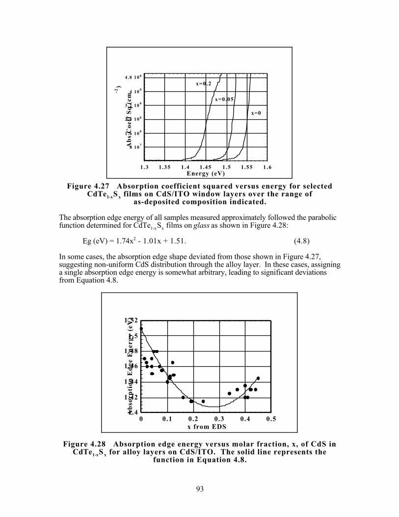
93
8 10 7
1 .6 10 8
2 .4 10 8
3 .2 10 8
4 10 8
4 .8 10 8
1.3 1.35 1 .4 1.45 1 .5 1.55 1 .6
Abs
Coe
ff S
q (c
m
-2)
Energy (eV)
x=0.2
x=0.05
x=0
Figure 4.27 Absorption coefficient squared versus energy for selectedCdTe1-xS x films on CdS/ITO window layers over the range of
as-deposited composition indicated.
The absorption edge energy of all samples measured approximately followed the parabolicfunction determined for CdTe1-xSx films on glass as shown in Figure 4.28:
Eg (eV) = 1.74x2 - 1.01x + 1.51. (4.8)
In some cases, the absorption edge shape deviated from those shown in Figure 4.27,suggesting non-uniform CdS distribution through the alloy layer. In these cases, assigninga single absorption edge energy is somewhat arbitrary, leading to significant deviationsfrom Equation 4.8.
1.4
1.42
1.44
1.46
1.48
1.5
1.52
0 0.1 0.2 0.3 0.4 0.5
Abs
orpt
ion
Edg
e E
nerg
y (e
V)
x from EDS
Figure 4.28 Absorption edge energy versus molar fraction, x, of CdS inCdTe1-xS x for alloy layers on CdS/ITO. The solid line represents the
function in Equation 4.8.

94
4 .3 .3 .2 Heat Treatment of Alloy Absorber Layer Films
The presence of CdS throughout the CdTe1-xSx absorber layer with x up to 0.06 did notmeasurably alter the recrystallization process or surface chemistry obtained after CdCl2treatment, allowing the same post-deposition processes to be used in all deviceconfigurations. For samples with as-deposited CdS content greater than 0.06, a singlephase was measured after deposition, but two phases, Te-rich cubic CdTe0.94S0.06 and S-rich hexagonal CdS0.97Te0.03, were detected after CdCl2 treatment (Figure 4.29). Glancingincidence XRD, Auger (measured at NREL) , and XPS (measured at NREL)measurements indicated that S-rich CdS1-yTey was distributed throughout the film, with thegreatest portion segregated to the free surface of the sample. This intriguing result dictatesthat for devices, where uniform Te-rich phase is desired, studies of uniform layers must berestricted to films with CdS compositions less than the miscibility gap concentration.
1.0
0.8
0.6
0.4
0.2
0.0
In
ten
sity
(A
U)
302826242220
2-Theta (deg)
40948.32 As Depθ/2θ MeasurementEDS x = 9% (4.5 at %)
1.0
0.8
0.6
0.4
0.2
0.0
In
ten
sity
(A
U)
302826242220
2-Theta (deg)
40948.32 CdCl2 HT 420C/20'Glancing Incidence, α = 1 degree
CdTe0.94S0.06Cubic (111)
CdS0.97Te0.03Hexagonal (002)
Figure 4.29 XRD spectra of single phase as-deposited CdTe0.91S 0.09 and thesame sample after heat treatment with CdCl2 at 420°C in air.
Using uniform layers with x < 6%, dramatic evidence for the retarding of CdS diffusioninto a CdTe0.95S0.05 layer under conditions of high CdCl2 concentration was found. This isapparent in the XRD line profiles of 2.5 µm thick samples (Figure 4.30). With CdTeabsorber layers, this CdCl2 treatment produced a broadened multi-modal distributionsignifying the presence of several discreet regions different compositions, equivalent to aCdS layer 110 nm thick. With the CdTe0.95S0.05 layer and the identical CdCl2 treatment, asingle sharp line profile centered on the Bragg angle for x = 0.05 was obtained, having asmall tail extending to x = 0.06, indicating a gain of an equivalent CdS thickness of lessthan 10 nm.

95
1.0
0.8
0.6
0.4
0.2
0.0
Inte
nsit
y (A
U)
77.076.0
2θ (deg)
Figure 4.30 XRD (511) line profile of 2.5 µm CdTe/0.2 µm CdS (dotted)and 2.5 µm CdTe0.95S 0.05/0.2 µm CdS (solid) after CdCl2 treatment
with high CdCl2 concentration.
The retarding of CdS-CdTe interdiffusion during post-deposition processing by using alloyabsorber layers was verified by EDS and XRD measurements for numerous samples.Structures of CdTe0.96S0.04 /CdS/ITO (x < solubility limit) were treated under conditionsknown to alter the extent of interdiffusion in CdTe/CdS/ITO samples. In some cases, ahigh temperature anneal (HTA) at 580°C was performed prior to CdCl2 vapor treatment asdescribed in References [136, 168, 170]. The EDS and XRD data do not reveal significantCdS uptake by the CdTe1-xSX films. The materials analysis results for CdTe/CdS/ITO andCdTe0.96S0.04/CdS/ITO are compared in Table 4.14 for three treatment conditions. High-resolution XRD profiles for the three treatment methods are shown in Figure 4.31.
Table 4.14 Treatment conditions and materials data for 2.5 µm thickabsorber layers on CdS/ITO after CdCl2 processing at 420°C for 30 minutesin air. The third sample in each group received a high temperature anneal(HTA) at 600°C for 15 minutes prior to CdCl2 vapor treatment.
FilmType
Treatment AGS
(µm)
EDSx
±0.3(%)
XRDao
(Å)
XRDx
±0.3(%)
XRD
Profile
XRD
p(111)
CdTe CdCl2:MeOH 1.0 1.0 6.475 1.0 Multi 0.5CdTe Vapor CdCl2 1.0 0.5 6.477 0.5 Asymm 1.0CdTe HTA + CdCl2 2.0 <0.3 6.479 0.3 Asymm 1.0
CdTe1-xSx CdCl2:MeOH 1.1 4.8 6.446 5.3 Symm 1.1CdTe1-xSx Vapor CdCl2 1.0 4.0 6.456 5.3 Symm 1.0CdTe1-xSx HTA + CdCl2 1.9 5.4 6.444 5.6 Symm 0.6

96
CdTe/CdS/ITO CdTe1-xSx/CdS/ITO1.0
0.8
0.6
0.4
0.2
0.0
Norm
aliz
ed Int
ensi
ty
77.276.876.476.0
2θ (deg)
1.0
0.8
0.6
0.4
0.2
0.0
Norm
aliz
ed Int
ensi
ty
77.276.876.476.0
2θ (deg)
1.0
0.8
0.6
0.4
0.2
0.0
Norm
aliz
ed Int
ensi
ty
77.276.876.476.0
2θ (deg)
1.0
0.8
0.6
0.4
0.2
0.0
Norm
aliz
ed Int
ensi
ty
77.276.876.476.0
2θ (deg)
1.0
0.8
0.6
0.4
0.2
0.0
Norm
aliz
ed Int
ensi
ty
77.276.876.476.0
2θ (deg)
1.0
0.8
0.6
0.4
0.2
0.0
Norm
aliz
ed Int
ensi
ty
77.276.876.476.0
2θ (deg)
Figure 4.31 X-ray diffraction line profiles for CdTe1-xS x after chlorideprocessing at 420°C for 30 minutes in air. Top = CdCl2:MeOH;
Middle = CdCl2 vapor; Bottom = HTA + CdCl2 vapor.

97
In Table 4.14, the average grain size (AGS) was determined by SEM, which showeduniform surface grain morphology with no residue on vapor-treated samples. Sulfurcomposition was measured by energy dispersive x-ray spectroscopy (EDS) at 20 kV.Comparison with as-deposited CdTe1-xSx layers shows a drop in the S content after CdCl2treatment for the film treated with HTA prior to CdCl2 vapor, due to CdS vaporization fromthe surface during the HTA step. Last month it was reported that films with x > solubilitylimit undergo phase segregation, with the S-rich phase on the surface. The precision latticeparameter, ao, is determined from the Te-rich component of the XRD (hkl) line profiles; thethree treatments chosen result in different S incorporation and asymmetry in line profile forCdTe films but constant lattice parameter and peak shape for CdTe1-xSx films.
The retarding effect obtained by using as-deposited CdTe1-xSx layers is also borne out byanalysis of the devices. Table 4.15 shows the change in CdS thickness after CdCl2treatment for pure CdTe, stepped alloy, and uniform alloy absorber layers for differentinitial CdS thicknesses. Comparing the devices with ~200 nm CdS, it is readily seen thatthe uniform alloy layer reduced CdS loss by more than 2X. The stepped layer was lesseffective, showing that the presence of the alloy near the solubility limit in the junction areais not sufficient to stop CdS diffusion. In the temperature-time regime used to make devicequality material, the quantity of CdS consumed is thus related to the deviation in absorberlayer composition from the miscibility gap composition. Notice that the difference betweenthe film compositions, x = 0.05, and the solubility limit, x = 0.06, allows a theoreticalmaximum of ~50 nm of CdS to be incorporated into a 5 µm thick alloy film. Thus, optimalcontrol of the quantity of CdS consumed during CdCl2 is achieved by depositing the alloyabsorber layer with composition as close as possible to the solubility limit for theprocessing temperature used.
Table 4.15 also shows device J-V data for cells with different alloy configurations. Thedevice Jsc increases as CdS final thickness is reduced. The Voc is relatively constant withCdS thickness until the final CdS thickness falls below 75 nm. It is possible that non-uniform CdS consumption produces regions of complete CdS loss which results information of parallel junctions between the absorber and TCO layers.
Table 4.15 CdS thickness from optical and QE data compared to device J-V parameters for different alloy configurations.
As-depositedStructure
Initiald(CdS)(nm)
Finald(CdS)(nm)
∆d(CdS)(nm)
Voc(mV)
Jsc(mA/cm2)
FF(%)
CdTe 200 60 140 753 22.0 59.2
Stepped Alloy 220 125 95 776 22.0 67.4(at junction 90 30 60 435 23.1 60.9x = 0.05) 50 20 30 412 25.0 60.0
Uniform Alloy 190 130 60 792 21.2 66.3(x = 0.05) 105 75 30 769 22.6 60.0
70 50 30 623 24.0 61.2
These results are graphically depicted for devices made with different alloy absorber layerconfigurations in Figure 4.32 and Figure 4.33. In Figure 4.32, the fall-off in Voc is shownfor initial and final CdS thickness on the same cells. Samples with uniform alloy absorber

98
layers exhibited the least change in CdS thickness. It is apparent from the convergence ofall devices onto the fall-off line for final CdS thickness that a fundamental mechanismwhich is independent of absorber layer configuration or composition dominates the deviceswith d(CdS) less than 100 nm. The open circles provide a significant clue; these are fordevices made with bi-layer SnO2 superstrates consisting of Libbey-Owens-Ford SnO2/glassover-coated with high resistivity SnO2 by Golden Photon, Inc. More will be reported onthis topic in the next section. Figure 4.33 shows that the Jsc values for this device groupapproach those predicted based on window layer optical transmission and a uniform 5%collection loss.
200
300
400
500
600
700
800
900
0 50 100 150 200 250
CdTe w/GPI SnO2Uniform CdTeSCdTeStepped CdTeS
Voc
(m
V)
di n i t
(CdS) (nm)300
400
500
600
700
800
900
0 50 100 150 200 250
Voc
(m
V)
df ina l
(CdS) (nm)
Figure 4.32 Voc versus CdS thickness for different alloy absorber layerconfigurations. Filled markers are for devices on ITO/7059.Open circles are for devices with bi-layer SnO2 superstrates,
to be discussed in the next section.
2 0
2 1
2 2
2 3
2 4
2 5
2 6
0 5 0 100 150 200
Jsc
(mA
/sq
cm)
d(CdS) (nm)
Max Jsc for ITO/7059w/ 5% Collection Loss
Figure 4.33 Jsc versus final CdS thickness in the devices of Figure 4.32.

99
4 .3 .3 .3 Modified Post-Deposition Heat Treatment
The diffusion of CdS into CdTe can also be controlled by reducing the number of availablediffusion pathways, which may be the single explanation needed to account for differencesin devices deposited by high and low deposition temperatures. In the CdTe/CdSstructures, the primary pathways are grain boundaries and crystallographic defects.Annealing the film at T > 550°C prior to chloride treatment enhances grain size, reducescrystallographic defects, and retards diffusion of CdS into CdTe [136, 168, 170]. As-deposited CdTe films have 200 nm wide columnar grains. An increase in grain size to 500nm prior to delivery of CdCl2 will reduce the total grain boundary area by ~5X, which willhave a significant effect on the grain boundary diffusion rate. The final structure canexhibit grains with lateral extent greater than 5 µm, i.e., an aspect ratio greater than 1(Figure 4.34).
Figure 4.34 SEM photographs of CdCl2 treated CdTe/CdS – no anneal(top) and HTA (bottom) prior to CdCl2 treatment.
The effect of the anneal step is also demonstrated by the XRD line profiles of CdTe/CdSsamples with 2.5 µm thick CdTe treated with CdCl2 vapor and treated with a 580°C annealfor 10 minutes prior to CdCl2 vapor treatment (Figure 4.35). The lateral grain size doubled

100
after the anneal; after CdCl2 treatment the grain size increased to the usual value of ~ 3 µm(aspect ratio of ~1). The XRD line profile is a sharp, instrumentally-limited profile with avery small tail, corresponding to an equivalent CdS thickness of less than 10 nm. Thesample which received no anneal exhibits a broad asymmetrical profile which correspondsto an equivalent CdS thickness of 100 nm. TEM cross-section micrographs of CdCl2treated samples with and without an anneal are shown in Figure 4.36; the annealed sampleexhibits a dense, uniform CdS layer after processing whereas the sample receiving CdCl2treatment only exhibits a discontinuous CdS layer after processing plus residualcrystallographic defects in the absorber layer.
1.0
0.8
0.6
0.4
0.2
0.0
Inte
nsit
y (A
U)
77.076.0
2θ (deg)
Figure 4.35 XRD (511) line profile of 2.5 µm CdTe/0.2 µm CdS afterCdCl2 vapor treatment (dotted) and after anneal in argon at 580°C
for 10 minutes followed by CdCl2 treatment (solid).
Figure 4.36 Cross-sectional TEM images of CdTe-CdS interface region onCdCl2-treated samples with anneal (left) and without anneal (right)
prior to chloride treatment.

101
The effect of changes in post-deposition processing on the change in CdS thickness and onthe device J-V behavior is shown in Table 4.16. The samples were chosen to represent theinitial CdS thickness at which a drop in Voc has been observed for PVD samples processedwith standard CdCl2 treatment. Use of the anneal step reduced the CdS loss by 2X andyielded higher Voc and FF for the final CdS thicknesses shown. Devices with Voc > 850mV and conversion efficiencies of PVD devices greater than 12% have been fabricatedusing this treatment method. This data suggests that the explanation of the differences inperformance between devices made by high temperature and low temperature processes liesin the density of the CdS layer and residual defects in the absorber layer which are notcompletely removed by CdCl2 treatment.
Table 4.16 CdS thickness from optical and QE data and device parametersfor different heat treatments.
Method Initiald(CdS)(nm)
Finald(CdS)(nm)
∆d(CdS)(nm)
Voc
(mV)
Jsc
(mA/cm2)
FF
(%)CdCl2 Only 180 100 80 775 22.9 67.0
Anneal + CdCl2 180 150 30 795 21.0 70.0
CdCl2 Only 160 90 70 690 21.4 50.8Anneal + CdCl2 160 140 40 790 20.6 70.6
Anneal + CdCl2 130 115 15 705 21.5 57.9
Given that CdS diffusion into the absorber layer of CdTe-based superstrate thin-film solarcells is a limiting factor for fabrication control and device performance, it has been shownthat CdS loss can be reduced by depositing absorber layers having CdS content near thesolubility limit for the processing temperatures used or by reducing diffusion pathways inthe absorber layer by using a recrystallization step prior to CdCl2 treatment. Use of denserCdS layer or of a densification step, combined with these techniques is expected to furtherextend control over the CdS diffusion and improve device performance with ultra-thin as-deposited CdS layers in PVD devices. Use of alternative TCO superstrate structures,having a high resistivity layer in contact with CdS, may offer control of junction propertiesif parallel diodes exist between CdTe/CdS and CdTe/TCO.
The results of this work can be readily summarized:
• Primary device junction is CdTe1-xSx/CdS1-yTey.
• Te-S distribution is non-homogeneous in absorber layer.
• CdS loss via interdiffusion is a performance-controlling mechanism in superstrateCdTe/CdS devices, especially for:
⇒ Fabrication processes having diffusion-enhancing properties (high chlorideconcentration during deposition, sub-micron grains, etc);
⇒ CdTe/TCO junctions exhibiting high Jo.
• CdS-CdTe interdiffusion is reduced by:

102
⇒ CdTe1-xSx alloy absorber layer (minimize chemical driving force);
⇒ Thermal history (minimize grain boundary volume).
• Role of TCO/Absorber junction ==> Alternative TCO.
4 .3 .4 Influence of TCO
The parallel diode representation of the CdTe/CdS/TCO devices discussed in Section 4.3.1leads to the conclusion that a sufficient density of spatial discontinuities in the CdS layerwill result in a significant fraction of device area comprised of CdTe/TCO junctions. ForCdTe/ITO, the junction is characterized a diode current, Jo, one to two orders of magnitudehigher than that measured for CdTe/CdS junctions. Obviously, one approach is tominimize extrinsic discontinuities such as pinholes in as-deposited CdS films. In thisphase of the contract, pinholes were characterized and techniques were established to selector eliminate CdS/ITO/glass structures for CdTe depositions (see Section 4.3.1 above). InSection 4.3.3, it was further shown by TEM that the non-uniform depletion of CdS duringpost-deposition chloride treatment can be minimized by use of an anneal at T > 550°C.
Another approach, however, assuming that CdTe/TCO junctions always exist in deviceswhen d(CdS) is less than 100 nm, is improvement of the CdTe/TCO junction itself.Without a specific junction model for CdTe/TCO, however, it is difficult to suggest a priorihow to improve the junction, i.e., reduce Jo. It is also unclear that the CdTe/TCO junctionwill behave similarly to a CdTe/TCO junction in which a trace quantity of CdS was presentprior to treatment. The work of Golden Photon provided an existence proof for devices inwhich the CdS layer was completely consumed. According to a patent on spray processeddevices, a low conductivity tin oxide layer is formed on top of the current-carrying highconductivity tin oxide layer [171]. Such devices exhibit high Jsc and Voc, yet the quantumefficiency indicates no detectable CdS layer remaining.
As part of the activity of the CdTe Team, several experiments were conducted to explorethe effect of alternative TCO’s: 1) Use TiO2/SnO2; TiO2 has an optical bandgap of 3 eV,and 2) use TCO’s over-coated with low conductivity layers. Specifically, IEC fabricatedcells on: a) Harvard Nb-doped TiO2 on SnO2 made at the University of South Florida(USF); b) USF, SnO2; and c) bi-layer SnO2 made by Golden Photon, Inc (GPI).
TiO2/SnO2/Glass was rinsed with methanol and dried with flowing argon prior to CdSdeposition. Target figures for CdS thickness were 20 nm and 150 nm. CdS films wereCdCl2 vapor treated prior to CdTe deposition. CdTe was deposited 5 µm thick. Allstructures received high temperature anneal (600°C for 15 minutes) followed by CdCl2vapor treatment. Diffused copper plus etch process with graphite paste contacts were usedto make contact to the devices. J-V tests with forward and reverse voltage sweep weremade with xenon simulator at AM 1.5 conditions at 25°C. The best cell obtained for eachcase is shown in Table 4.17.

103
Table 4.17 Device fabrication conditions and J-V results using alternativeTCO.
Sample TCO di(CdS)(nm)
Voc(mV)
Jsc(mA/cm2)
FF(%)
Roc(Ω-cm2)
Gsc(mS/cm2)
984.21 TiO2/SnO2 160 751 22 61 6 2984.11 TiO2/SnO2 30 364 23 42 7 9985.13 TiO2/SnO2 0 563 23 49 7 5
984.12 SnO2 30 392 24 50 4 5
The TiO2 had little effect on the performance of the PVD cells. The best cells were obtainedon the piece with the thickest CdS, as found for SnO2 or ITO TCO’s. The voltage of thedevices with no CdS was surprisingly high and may be an effect of the TCO notexperiencing the CdCl2 vapor treatment. In a subsequent experiment with niobium-dopedTiO2 films, the CdTe deposition incurred a substrate control thermocouple failure whichresulted in only 3 µm film thickness. Also, the samples were plagued by delaminationduring CdCl2 treatment. Thus, the comparative aspect of the doped TiO2 experiment tobaseline results was not possible. In spite of these problems, devices were completed andtested. The significant result of this sample set was blocking forward bias J-Vcharacteristic not seen on the previous set with TiO2 (40984 - presented above). Thesecond set, which reached a much higher deposition temperature than set 40984, exhibitsthe same blocking characteristic near Voc as found by the other team members, suggestingan influence of the CdTe deposition temperature on the interaction between the TiO2 and theCdS/CdTe. Linear forward bias behavior has only been obtained on samples having theCdTe deposited at ~250°C. Aside from the blocking characteristic, which does not occuron samples with ITO or bare SnO2, no other systematic difference in performance wasfound for this sample set.
4 .3 .5 Conclusion
For the GPI superstrates, encouraging results were obtained with respect to Voc. The J-Vdata showed substantial Voc gains for the ultra-thin CdS compared to any other PVDdevices that have been made with such thin CdS on single layer ITO/7059, SnO2/7059, orSnO2/SL glass (Figure 4.32). As a reference, the best previous device we have made withultra-thin evaporated CdS (d ~ 50 nm) utilized a CdTe0.95S0.05 alloy absorber layer andgave: Voc = 623 mV; Jsc = 24.0 mA/cm2; FF = 61.2%; for Eff = 9.1%. The cells in thepresent experiment have CdTe absorber layers, which with ITO typically yields Voc nogreater than 400 mV for d(CdS) ~ 50 nm. The present devices yield: Voc = 715 mV; Jsc =24 mA/cm2; FF = 65%; for Eff = 11.1%. Thus, the properties of the GPI SnO2 bilayer arewell-suited for the PVD process. Additional samples with the GPI SnO2 and with bi-layerITO will be processed in 1998 and will be electrically characterized.
4.4 CdTe Contacting in Device Structures
4 .4 .1 Introduction
The most delicate feature of the CdTe/CdS device is believed to be the low loss backcontact. Low resistance contacting methods typically involve use of Te-rich interfaces or p-type semiconductors such as HgTe or ZnTe, or thin layers including small amounts of Cu.Some devices subjected to stress testing or life testing display high series resistance and/or

104
evidence of a reverse diode, both characteristics which could be attributed to the backcontact. What will be presented is an attempt to summarize and construct a simple workinghypothesis of the important points gleaned from the stress tests and measurements done atIEC. Some of the details of these tests and measurements have been previously published[172 & 173].
4 .4 .2 Physio-chemical Analysis of Contact Operation
Forming low resistance Ohmic electrical contacts to p-type CdTe can be accomplished bymany techniques [152]. For single crystals of CdTe, the CdTe conductivity and the workfunction of the contact material are critical, and for crystals with sufficient conductivity,doped to > 1014 cm-3, high work function materials such as gold and carbon are effective.For polycrystalline thin-films, however, the physical and chemical state of the grain andintergranular surface are substantially different from single crystal cases. For example, inthin-film devices, obtaining high internal quantum efficiency requires various treatmentswith oxygen and halogens to establish appropriate junction properties. Thus, while theinterior of a given grain may be sufficiently p-doped, its surface may be composed of acomplicated structure of oxides and halides. It is even possible that the reaction chemistrybetween the film and ambient (halogen-oxygen) treatment could produce Cd excess at theback surface, reducing p-type conductivity. Also, enhanced p-type doping along grainboundaries (normal to the CdS-CdTe interface) is required to minimize minority carrierrecombination for carriers generated outside the space-charge region [137].
It is therefore necessary to “undo” the surface condition brought about by the junction-forming treatments to permit formation of Ohmic contacts. Over the past decade, IEC hasemployed a copper diffusion step to dope along grain boundaries, coupled with one ormore etch steps to remove excess Cd, produce Te excess, and remove excess Cu metal[152]. This year, the crystalline phase composition of the surface of CdTe was measuredin working devices, revealing the presence of Cu2Te (Figure 4.37). Thus, the chemistry ofthe steps used to form contacts to CdTe can be written:
CdTe + Br2 ==> Te + CdBr2 (∆Grxn = -48 kcal/mol) (4.9)
CdTe + 2 Cu + Br2 ==> Cu2Te + CdBr2 (∆Grxn = -59 kcal/mol) (4.10)
Note that the reaction product CdBr2 is soluble in methanol. If the etch is performed priorto Cu deposition, the reaction to form Cu2Te is spontaneous:
Te + 2 Cu ==> Cu2Te (∆Grxn = -12 kcal/mol) (4.11)

105
1000
800
600
400
200
0
Inte
nsity
(t=2
sec
)
90807060504030202θ (deg)
+ Cu2Teo Cr
o
o
+
+ +
+
+ + ++
Figure 4.37 Glancing incidence (4°) x-ray diffraction pattern of CdTedevice through thin chromium metal contact showing Cu2Te phase.
Signatory electrical characteristics which are encountered, such as forward bias curvature,light-to-dark crossover, and high series resistance (Roc > 8 ohm-cm2), are indicative of acombination of insufficient p-type doping or existence of a blocking primary contact toCdTe. By using a brief etch in hydrazine prior to Cu deposition, substantially more Teexcess is formed, resulting in a more tolerant process. Recent cell results for CdTe/CdSand CdTeS/CdS junctions obtained using hydrazine etch are listed in Table 4.18. Alsolisted are results for a representative cell fabricated with CdTe/CdS from Solar Cells, Inc.and contacted at IEC using the same process with carbon conductor.
Table 4.18 Device fabrication steps and J-V results for cells withhydrazine etch prior to copper deposition.
Sample Absorber d (CdS)(µm)
HighTempStep
Voc(mV)
Jsc(mA/cm2)
FF(%)
Eff(%)
Roc(Ω-cm2)
929.21 CdTe 0.19 Y 789 21.7 70.6 12.1 3.8978.22 CdTe 0.20 Y 795 21.5 68.4 11.7 3.8934.11 CdTe0.96S0.04 0.25 Y 760 20.7 60.3 9.5 5.1948.231 CdTe0.94S0.06 0.18 N 710 19.0 65.5 8.8 5.52D3.3 SCI ~0.24 Y 821 19.7 73.2 11.8 4.3
As the Roc and FF values show, the contact process is moderately well-optimized forstructures with CdTe and CdTeS and for CdTe/CdS from SCI. The devices exhibited no J-V retrace hysteresis and no crossover between dark and light traces.

106
4 .4 .3 Electronic Analysis of Contact Operation
We have found that most of the changes in the J-V characteristic due to stress conditionscan be divided into two broad categories: (1) a “blocking contact,” “rollover” or “leakydiode” appears in the J-V behavior in forward current bias (we define this as the occurrenceof a minimum in the dV/dJ characteristic for J > 0); (2) an overall “shift” of the J-Vcharacteristic to a lower voltage (this usually becomes apparent in a log J vs. V plot) whichcan also be accompanied by an increase in series resistance (in the illuminated J-Vcharacteristic this results in a change in Voc and in FF with little or no change in Jsc); and (3)both changes occur together.
Analysis of contacts to CdTe in working devices was carried out to elucidate the nature of“blocking contact” behavior which onsets at low temperature and which develops afterstressing of cells at open circuit at 100°C. The J-V testing of unstressed cells was carriedby varying the testing temperature to determine the activation energy of the blockingbehavior and by varying the illumination intensity to separate out the photoconductiveeffects in the CdTe. To do these analyses, a simple equivalent circuit model incorporating aback diode was used, and the corresponding current equations were solved to separate thecontact resistance. Results for a baseline cell completed using wet contact chemistry show:linear Voc versus T (J = 0 bias point not affected by contact); Voc at 0 K = 1.43 Volt; andactivation energy for series resistance of 0.3 eV as shown in Figure 4.38 and Figure 4.39.
0.5
0.6
0.7
0.8
0.9
1
200 250 300 350 400
-50 0 50 100
T [K]
VOC (T = 0 K) = 1.43 V
T [°C]
Figure 4.38 Voc vs T for device #40929-21-5 at AM1.5G.

107
0.1
1
10
32 34 36 38 40 42 44
q/kT (eV)-1
φ ≈ 0.3 eV
Figure 4.39 Series resistance versus 1/T for the same deviceshown in Figure 4.38.
4 .4 .4 Stress Testing and Analysis
Cells completed with IEC contacts on CdS/CdTe by Solar Cells, Inc. were stressed atColorado State University (100°C, 2 suns, 6 weeks) and were returned to IEC. The beforeand after stressing J-V behavior is shown in Figure 4.40 and Figure 4.41.
- 2 0
- 1 5
- 1 0
- 5
0
5
10
-0 .4 -0 .2 0 0 .2 0 .4 0 .6 0 .8 1
J(m
A/s
qcm
)
V(Volts)
20632D3-3-1
Figure 4.40 J-V behavior of SCI cell with IEC carbon contactbefore stressing.

108
- 2 0
- 1 5
- 1 0
- 5
0
5
10
-0 .5 0 0 .5 1J(
mA
/sqc
m)
V(Volts)
20632D3-3-1
Figure 4.41 J-V behavior of same cell after stress at 100°C, 2 suns,6 weeks @ Voc.
These cells then had their contacts removed and re-applied to help separate the location inthe structure of whatever effect is responsible for the change in J-V behavior.
After being returned to IEC, one device was recontacted by lifting off the original carboncontact, re-etching the surface in 0.01% bromine-methanol for 2 seconds, and reapplyingthe carbon contact. The J-V data are shown in Table 4.19 and Figure 4.42 for the initial,stressed, and recontacted conditions.
Table 4.19 Device results for device # SSI 20632D3-3-1.
Eff(%)
FF(%)
VOC (Volts)
JSC(mA/cm2)
ROC(Ω-cm2)
GSC(mS/cm2)
TestDate
Initial 11.79 73.3 0.8192 19.65 4.40.0 Dark0.4 AM1
Feb28
After Stress @ CSU(100°C, 2 suns, 6 weeks, VOC) 7.17 53.6 0.7273 18.39 20.2
0.0 Dark2.4 AM1
Nov12
ContactsRemoved & Reapplied 9.08 62.2 0.7308 19.98 4.7
0.0 Dark1.2 AM1
Nov20

109
-30
-20
-10
0
10
20
30
40
50
-0.5 0 0.5 1 1.5
Initial
Degraded
ReContact
V (Volts)
Figure 4.42 Summarized J-V behavior of device # SSI 20632D3-3-1.
The initial dark I-V characteristic of the device can be represented by a simple diode andresistor
J = J0 exp[(V-RSJ)/V0] (4.12)
and is shown in Figure 4.43 and Figure 4.44. After degradation the dark I-V exhibits a“blocking contact” behavior with a diode behavior similar to before degradation ( Figure4.44). The results of the model fit are shown separately in Table 4.20. After the previousC contact lifted, CdTe etch and new C contact applied, the dark I-V “blocking contact”behavior is reduced but the main diode behavior is unchanged ( Figure 4.44).
0.01
0.1
1
10
100
0.5 0.6 0.7 0.8 0.9 1
Initial J-V
Data
Equation
V (Volts)
J=J0 exp[(V-R
SJ)/V
0]
J0=3.3x10⁻⁸ mA/cm2
V0=0.041 Volts
RS=1.6 Ω-cm2
Figure 4.43 Dark J-V data and equivalent circuit fit forbefore degradation.

110
0.01
0.1
1
10
100
0.4 0.5 0.6 0.7 0.8 0.9 1
InitialDegradedReContact
V (Volts)
Figure 4.44 Summarized dark J-V data and equivalentcircuit diode parameters.
Table 4.20 Diode parameters of the straight line fits shown inFigure 4.44.
V0(Volts)
J0(mA/cm2)
Initial 0.041 3.3x10 -8
After Stress @ CSU (100°C, 2 suns, 6 weeks, VOC) 0.041 8.0x10 -7
ContactsRemoved & Reapplied 0.041 8.0x10 -7
Figure 4.45 shows the J-V slope (dJ/dV) in reverse and low forward voltage of the J-Vcurve in the three conditions. The initial illuminated I-V behavior shows the normal“displaced” dark I-V curve with a small amount of J L(V) behavior. After degradation theilluminated I-V is dominated by the J L(V) behavior. After previous C contact lifted, CdTeetch and new C contact applied, the J L(V) behavior is essentially unchanged. This datacan be interpreted as a reduction in the p-type doping of the CdTe layer by the stresscondition, manifested in a lower junction voltage and development of a blocking contact.Re-contacting restores most of the contact portion of the degradation but does not affect themain junction.

111
0
2
4
6
8
10
-0.5 0 0.5
InitialDegradedReContact
V (Volts)
Illuminated Dark
Figure 4.45 Summarized dJ/dV behavior of device # SSI 20632D3-3-1.
4 .4 .5 Operational Model
It is possible to look at the observations as resulting from a single mechanism. If a dopant(or compensating material) is activated by temperature and affected by an electric field (i.e.,charged), it can account for the basic J-V behaviors. Under forward electrical bias it wouldaccumulate at the contact, giving rise to the blocking contact behavior. Its concentrationwould also be depleted in the bulk and junction areas, thereby causing the J-V shift andincreased series resistance. When reverse electrical bias is applied, it would move towardthe metallurgical main junction, whose behavior is already “blocking.” This would stillreduce its concentration in the rest of the CdTe, giving rise to only the J-V shift andincreased series resistance.If the p-type dopant is accumulating at the contact during forward bias stress, it should bepossible to remove it, and redope and recontact the device. To test this, we are exposingcontacted and uncontacted material to temperatures of about 100°C under illumination(@ Voc). When the contacted material exhibits the blocking contact and J-V shift behavior,one uncontacted piece will be etched and contacted, and another will be etched, doped andrecontacted. We expect to see the etched and contacted piece behave as if it were etchedand recontacted (i.e., at room temperature, the blocking contact behavior disappears, butthe J-V shift remains), while the etched and doped sample should appear as the normalinitial I-V behavior.

112
5. AbstractThis report describes results achieved during phase I of a four-phase subcontract to developand understand thin film solar cell technology associated to CuInSe2 and related alloys, a-Siand its alloys and CdTe. Modules based on all these thin films are promising candidates tomeet DOE long-range efficiency, reliability and manufacturing cost goals. The criticalissues being addressed under this program are intended to provide the science andengineering basis for the development of viable commercial processes and to improvemodule performance. The generic research issues addressed are: 1) quantitative analysisof processing steps to provide information for efficient commercial scale equipment designand operation; 2) device characterization relating the device performance to materialsproperties and process conditions; 3) development of alloy materials with differentbandgaps to allow improved device structures for stability and compatibility with moduledesign; 4) development of improved window/heterojunction layers and contacts to improvedevice performance and reliability; and 5) evaluation of cell stability with respect toillumination, temperature and ambient and with respect to device structure and moduleencapsulation.

113
6. References 101. W.N. Shafarman, R. Klenk, and B.E. McCandless, J. Appl. Phys. 79(9), 7324
(1996).102. W.N. Shafarman, R. Klenk, and B.E. McCandless, Proc. of 25th IEEE PVSC, 763
(1996).103. J.E. Phillips, J. Titus, and D. Hofmann, Proc. of 26th IEEE PVSC, 463 (1997).104. S.S. Hegedus and J.E. Phillips, Proc. IEEE First World Conf. on Photovoltaic
Energy Conversion, 654 (1994).105. S.S. Hegedus, Progress in Photovolt. Res. Appl. 5 , 151 (1997).106. C. Dzionk, H. Metzner, S. Hessler and H.-E. Mahnke, Thin Solid Films 299 , 38
(1997).107. V. Nadenau, D. Braunger, D. Hariskos, M. Kaiser, Ch. Koble, A.. Oberacker, M.
Ruckh, U. Ruhle, R. Schaffler, D. Schmid, T. Walter, S. Zweigart and H.W.Schock, Progress in Photovoltaics: Research and Applications 3 , 363 (1995).
108. T. Nakabayashi, T. Miyazawa, Y. Hashimoto and K. Ito, Solar Energy Materialsand Solar Cells 49 , 375 (1997).
109. M.L. Fearheiley, H.J. Lewerenz.and M. Fuentes, Solar Energy Materials, 19 , 167(1989).
110. I.V. Bodnar, I.N. Tsyrelchuk and I.A. Victorov, Journal of Material Science Letters13 , 762 (1994).
111. W. Gebicki, M. Igalson, W. Zajac and R. Trykozko, J. Physics D: Applied Physics23 , 964 (1990).
112. F. Itoh, O. Saitoh, K. Kita, H. Nagamore and H. Oike, Solar Energy Materials andSolar Cells 50 (1998).
113. W.N. Shafarman, R.W. Birkmire, M. Marudachalam, B.E. McCandless. and J.M.Schultz, AIP Conference Proceedings 394 , 123 (1997)
114. K. Granath, A. Rockett, M. Bodegård, C. Nender and L. Stolt, 13th PV SolarEnergy Conference, Nice, France (1994).
115. M. Bodegård, L. Stolt and J. Hedstrom, 13th PV Solar Energy Conference, Nice,France, 1743 (1994).
116. W.E. Devaney, W.S. Chen, J.M. Stewart and R.A. Mickelsen, IEEE Trans.Electron Devices 37 , 428 (1990).
117. R. Klenk, T. Walter, H.W. Schock, and D. Cahen, Advanced Material 5 , 115(1993).
118. L.C. Olsen, W. Lei, F.W. Addis, W.N. Shafarman, M. Contreras, and K.Ramanathan, Proc. 26th IEEE Photovoltaic Specialists Conference, 363 (1997).
119. J. Sites and J. Hiltner, “Heat and Light Stress Measurements on Siemens SolarMinimodules,” presented at the Thin Film Photovoltaics Partnership Programmeeting in Anaheim, CA, Sept. 29, 1997.
120. D. Willett and S.Kuriyagawa, Proc. 23rd IEEE Photovoltaic Specialists Conference,495 (1993).

114
121. Th. Meyer, M. Schmidt, R. Harney, F. Engelhardt, O. Seifert, J. Parsai, M. Schmitt
and R. Rau, Proc. 26th IEEE Photovoltaic Specialists Conference, 371 (1997).122. M. Igalson and H.W. Schock, J. Appl. Phys. 80(10), 5765 (1996).123. R.W. Birkmire and J.E. Phillips, Final Report to NREL under Contract XAV-3-
13170-01 for the period January 16, 1993 to January 15, 1997, report date May1997.
124. C. Wronski, R. Collins, H. Fujiwara, L. Jiao, Y. Lee, S. Semoushkina, S. Kim, Z.Lu, H. Liu and J. Koh, Annual Technical Report for NREL Contract #XAN-4-13318-03 for the period July 1995 to July 1996, report date January 1997.
125. Q. Wang, Y. Xu and R. Crandall, AIP Conference Proc. 353 (13th NREL PVProgram Review) 473 (1996).
126. S. Hegedus, H. Liang and R. Gordon, “Transparent conducting oxides foramorphous silicon solar cells,” AIP Conference Proc. 353 (13th NREL PV ProgramReview), 465 (1996).
127. R. Gordon, Proc. MRS Symp. 426 , 419 (1996).128. M. Kubon, et al. Proc. 1st WCPEC, IEEE Press, 500 (1994).129. S.Hegedus, W. Buchanan, X. Liu and R. Gordon, Proc. 25th IEEE PVSC,
Washington DC, IEEE Press, 1129 (1996).130. R.W. Birkmire, et al., IEC Annual Report to NREL under subcontract #XAV-3-
13170-01, for the period 1/16/94 - 1/15/95, January 1995, p. 39.131. B.E. McCandless and R.W. Birkmire, Solar Cells 31 , 527-535 (1991).132. R.W. Birkmire, et al., IEC Annual Report to NREL under subcontract #XAV-3-
13701-01, for the period 1/16/94 - 1/15/95, January 1995, p. 30.133. A. Rohatgi, Int. J. Solar Energy 12(1-4), 43 (1992).134. D. Albin, CdTe Team Meeting Notes, January 22, 1996.135. J. Kester and S. Albright, Annual Report to NREL under Subcontract ZAF-5-14142-
06, Sept. 1995 - Aug. 1996, p. 4.136. B.E. McCandless, R.W. Birkmire, D.G. Jensen, J.E. Phillips and I. Youm, AIP
Conf. Proc. 394 , 647-654 (1996).137. J.E. Phillips, R.W. Birkmire, B.E. McCandless, P.V. Meyers and W.N.
Shafarman, phys. stat. sol. (b) 194 , 31 (1996)138. B.E. McCandless, L.V. Moulton and R.W. Birkmire, Prog. in Photovoltaics 5 , 249
(1997).139. I. Clemminck, M. Burgelman, M. Casteleyn, and B. Depuydt, Int. J. of Solar
Energy 13(1-4), 67 (1992).140. A. Rohatgi, S.A. Ringel, R. Sudharsanan and H.C. Chou, Proc. 22nd IEEE
Photovoltaic Specialists Conference, 962 (1991).141. B.E. McCandless and S.S. Hegedus, Proc. 22nd IEEE Photovoltaic Specialists
Conference, 967 (1991).142. R.W. Birkmire, et al., IEC Annual Report to NREL under subcontract #XAV-3-
13170-01, for the period 1/16/93 - 1/15/94, March 1994, p. 84.143. I. Youm. B.E. McCandless and R.W. Birkmire, Manuscript in preparation.

115
144. B.E. McCandless, H. Hichri, G. Hanket and R.W. Birkmire, Proc. 25th IEEE
Photovoltaic Specialists Conference, 781 (1996).145. D.H. Rose, D.H. Levi, R.J. Matson, D.S. Albin, R.G. Dhere and P. Sheldon,
Proc. 25th IEEE Photovoltaic Specialists Conference, 778 (1996).146. Y. Qu, P.V. Meyers and B.E. McCandless, Proc. 25th IEEE Photovoltaic
Specialists Conference, 1013 (1996).147. R.W. Birkmire, H. Hichri, R. Klenk, M. Marudachalam, B.E. McCandless, J.E.
Phillips, J.M. Schultz and W.N. Shafarman, AIP Conf. Proc. 353 , 410 (1995).148. D.G. Jensen, B.E. McCandless and R.W. Birkmire, Proc. 25th IEEE Photovoltaic
Specialists Conference, 773 (1996).149. B. Basol, Int. J. of Solar Energy 12(1-4), 25 (1992).150. M. Nishitani, K. Hisamoto, M. Ikeda and T. Hirao, Jap. J. of Appl. Phys. 29(8),
L1376 (1990).151. J.A. von Windheim and M. Cocivera, J. Phys. D: Appl. Phys. 23 , 581 (1990).152. B.E. McCandless, Y. Qu and R.W. Birkmire, Proc. 1st World Conference on
Photovoltaic Energy Conversion, 107 (1994).153. D.H. Levi, L.M. Woods, D.S. Albin, T.A.Gessert, D.W. Niles, A. Swartzlander,
D.H. Rose, R.K. Ahrenkiel and P. Sheldon, Proc. 26th IEEE PhotovoltaicSpecialists Conference, 351 (1997).
154. B.E. McCandless, H. Hichri, G. Hanket and R.W. Birkmire, Proc. 25th IEEEPhotovoltaic Specialists Conference, 781 (1996).
155. S.C. Jackson, et al., AIChE Journal 33(5), 711 (1987).156. G.B. Harris, Phil. Mag. 43 , 113 (1952).157. J.B. Nelson and D.P. Riley, Proc. Phys. Soc. 57 , 160 (1945).158. A. Taylor and H. Sinclair, Proc. Phyts. Soc. 57 , 126 (1945).159. R.A. Young and D.B. Wiles, J. Appl. Cryst. 15 , 430 (1982).160. B.E. McCandless, in Processing and Modeling Issues, Annual Report to NREL,
Subcontract #XAV-3-13170-01, p. 36 (January 1995).161. B.E. Warren, X-Ray Diffraction, London (1969).162. D.G. Jensen, B.E. McCandless and R.W. Birkmire, Mat. Res. Soc. Proc. 426 , 325
(1996).163. K. Ohata, J. Saraie and T. Tanaka, Japan. J. Appl. Phys. 12 , 1641 (1973).164. S. Nunoue, T. Hemmi and E. Kato, J. Electrochem. Soc. 137 , 1248 (1990).165. D.G. Moon and H.B. Im, Powder Metalurgy 35(1), 53 (1992).166. R. Venugopal, Master’s Thesis, Materials Science Program, University of Delaware
(January 1997).167. B.E. McCandless, R.W. Birkmire, D.G. Jensen, J.E. Phillips and I. Youm, Proc.
14th NREL PV Program Review Meeting (ARD), Lakewood, CO, November 1996.168. B.E. McCandless and I. Youm, Progress in Photovoltaics (accepted for publication,
February 1998).

116
169. “CdTe Team Meeting Notes” (January 22, 1996).170. R.W. Birkmire and J.E. Phillips, Processing and Modeling Issues for Thin-Film
Solar Cell Devices, Final Report, NREL Subcontract XAV-3-13170-01 (1997).171. S.P. Albright and R.R. Chamberlin, U.S. Patent 5,501,744 (1996).172. P.V. Meyers and J.E. Phillips, Proc. 25th IEEE Photovoltaic Specialists
Conference, 789 (1996).173. R.W. Birkmire, J.E. Phillips, W.A. Buchanan, et al., Final Report, NREL
Subcontract No. XAV-3-13170-01, 1/16/93 to 1/15/97, Section 4, p. 125 (1997)(this document can be downloaded in pdf format from eitherhttp://www.udel.edu/iec/pubs/final_rpt.html orhttp://www.nrel.gov/research/pv.iec_93-92.pdf).

Appendix 1
DETERMINING THE VOLTAGE DEPENDENCE OF THE LIGHT GENERATED CURRENT IN CuInSe2 -BASED SOLAR CELLS USING I-V MEASUREMENTS MADE AT DIFFERENT LIGHT INTENSITIES
J. E. Phillips, J. Titus and D. HofmannInstitute of Energy Conversion
University of DelawareNewark, DE 19716-3820 USA
ABSTRACT
As the bandgap of CuInSe2 is increased by alloying with
Ga or S, the loss in efficiency due to the decrease of lightgenerated current with increasing voltage becomesimportant. The standard technique of quantifying this lossis to analyze spectral response measurements made as afunction of applied voltage. Instead, it is shown how todetermine the voltage dependence of the light generatedcurrent by an analysis of the current-voltage (I-V)measurements made at two different light intensities. Byadding an I-V measurement at a third light intensity onecan also determine if the analysis technique is valid.
INTRODUCTION
It has been demonstrated that the loss in efficiency ofCu(In,Ga)Se2 solar cells with high Ga content is due to a
decrease in fill factor, and to a lesser extent Voc which is
caused by a drop in the light generated current withincreasing forward voltage [1 and 2]. This type of lossmechanism is well known in amorphous silicon solar cellswhere I-V measurement and analysis techniques havebeen developed to determine the voltage dependence ofthe light generated current, JL(V), [3 and 4].
ANALYSIS
In most solar cells, it is possible to correct for parasiticresistive losses by determining (eq. 1 & 3) and subtracting(eqs. 2 & 4) small shunt, Rshunt , and series resistance
,Rseries, terms from the measured J and V respectively.
1/Rshunt = Gshunt ≈ (dJ/dV)min. (1)
J' = J− V/Rshunt (2)
Rseries ≈ Limit1J→0
dV/dJ( ) (3)
V' = V − JRseries (4)
Which then gives the junction current, JJ(V'), and the
voltage dependent light generated current, JL(V'), (eq. 5).
If JJ(V') is independent of light intensity and JL(V') is
proportional to the light intensity, JL(V') can be found by
subtracting the J-V data measured at two different lightintensities (1 &2) with the same spectral content (eq. 6).
J' (V') = JJ(V') − JL(V') = JJ(V') − η V'( )JLmax (5)
J21 V'( ) ≡ J2' V'( ) − J1
' V'( ) = η V'( ) JL1max− JL2max
(6)
It is then possible to determine if the assumptions arecorrect by taking the difference between more than twolight intensities and comparing the results. i.e.
η(V') = J21 V'( )J21 V'( )max.
(7)
and:
η(V') = J31 V'( )J31 V'( )max.
(8)
EXPERIMENTAL PROCEDURE
J-V measurements were made on Cu(In,Ga)Se2 solar cells
at four different light intensities: (1) full AM1.5 Global
normalized to 100 mW/cm2, (2) ~90% AM1.5, (3) ~10%AM1.5 and (4) dark (Figure 1). The reduced lightintensities were achieved using neutral density screens.Two high light intensities (full & ~90%) and two low lightintensities (~10% & dark) were chosen to give accurate
comparisons when subtracting the J'-V' data. Rshunt was
determined from finding the minimum dJ/dV ,usually fromthe dark data, in reverse voltage bias (Figure 2). Rseries

was found from the intercept of dV/dJ vs. 1/J (Figure 3).The lower light intensities, ~10% and dark, are used to inthe Rseries determination in order to reduce interference
from JL(V) effects. Figure 4 shows the dark J-V data with
and without corrections for the parasitic resistance losses(eqs. 2 & 4). After correcting all the data for these losses,the high intensity J'-V' data were subtracted from the lowintensity data (eqs. 5 & 6). The normalized results of thissubtraction are shown in Figure 5. As can be seen fromFigure 5, except for high forward voltage bias, the differentsubtractions are basically identical. This shows that theassumptions that JJ(V') is independent of light intensity
and JL(V') is proportional to the light intensity are valid.
Finally, Figure 6 compares the full intensity J-V dataassuming that JL(V) was independent of voltage i.e.
JL(V)=JL(V)max.
-30
-20
-10
0
10
20
30
40
50
-0 .4 -0 .2 0 0 .2 0 .4 0 .6
J (
mA
/cm
2)
V (Vol t s )
Full~90%
~10%
Dark
Figure 1 J-V measurements for a Cu(In,Ga)Se2 solar cell
measured at various light intensities under anAM1.5Global spectrum (the J-V parameters for this deviceare underlined and bolded in Table 1).
0
1
2
3
4
-0 .4 -0 .2 0 0 .2
dJ
/dV
(m
S/c
m2
)
V (Vol t s )
Full ~90%
~10%
Dark
RShunt≈1.4 (kΩ-cm 2)
Figure 2 dJ/dV data for the solar cell shown in Figure 1
0
2
4
6
8
10
0 0.05 0 .1 0 .15 0 .2
Dark
~10%
dV
/dJ
(Ω
-cm
2)
[J+JSC
]- 1
(cm2
/mA)
RSeries≈0.5 (Ω-cm 2)
Figure 3 dV/dJ data for the solar cell shown in Figure 1

0 .1
1
10
100
0 .1 0 .2 0 .3 0 .4 0 .5 0 .6 0 .7
J (
mA
/cm
2)
V (Vol t s )
J-V Corrected for:
RSeries=0.5 (Ω -cm2)
RShunt=1.4 (kΩ -cm2)
Measured J-V
Figure 4 Dark J-V data, with and without resistancecorrections data for the solar cell shown in Figure 1.
0 .4
0 .5
0 .6
0 .7
0 .8
0 .9
1
-0 .4 -0 .2 0 0 .2 0 .4 0 .6
J'Dark-J'FullJ'10%-J'FullJ'Dark-J'90%J'10%-J'90%
η(V
')
V ' (Volts)
Figure 5 Normalized JL(V') data for the solar cell shown in
Figure 1
-30
-20
-10
0
10
20
30
40
50
-0 .4 -0 .2 0 0 .2 0 .4 0 .6
Measured J-V
J-V without JL(V) Loss
J (
mA
/cm
2)
V (Vol t s )
Figure 6 J-V data, with and without JL(V) losses, for the
solar cell shown in (the J-V parameters for this device areunderlined and bolded in Table 1).
RESULTS AND CONCLUSIONS
Table 1 shows the results of the previously describedmeasurements and analysis when applied to variousCu(In1-XGaX)Se2 solar cells. The solar cells used for this
analysis were chosen from two categories: (1) moderateGa content (X≈0.3) and fairly high efficiency and (2) highGa content (X=0.5 –> 0.7) and high Voc. As can be seen
from this table, the JL(V) losses, which varies from cell to
cell, primarily affects FF and Voc and hence Eff. However,
unlike the best devices examined in references 1 and 2,these JL(V) losses do not obviously increase with
increasing Ga content.
It can be concluded that, by taking J-V measurements atleast three different light intensities, one can determine ifit is correct to analyze these data for JL(V) losses and, if
correct, what the magnitude of these losses are.
ACKNOWLEDGEMENTS
The authors would like to thank J. Laker and the technicalstaff of the Institute of Energy Conversion. This work wassupported by the National Renewable Energy Laboratoryunder subcontract #XAK-7-17609-01.

Measured at AM1.5 Global @100mw/cm2
T = 30 deg. C; Area = 0.13 cm2
Derived Series andShunt Resistances
Calculated AM1.5 Global J-V parameterswithout JL(V) loss i.e. JL = JL(V)max.
Eff Voc FF Jsc Rseries Rshunt Eff Voc FF Jsc
(%) (Volts) (%) (mA/cm2) (Ω-cm2) (kΩ-cm2 (%) (Volts) (%) (mA/cm2)
High Efficiency Cu(In1-XGax)Se2 X≈0.3
13.9 0.606 68.8 33.2 0.2 1.7 15.1 0.635 71.0 33.5
13.6 0.631 72.1 29.8 0.1 2.5 14.2 0.644 73.6 30.0
12.8 0.583 67.8 32.4 0.0 0.7 13.7 0.607 69.4 32.6
12.8 0.605 68.2 31.0 0.0 1.7 13.5 0.626 69.3 31.1
12 .6 0 .612 66 .2 31 .1 0 .5 1 .4 14 .5 0 .637 71 .9 31 .7
12.5 0.596 63.9 32.9 0.4 1.1 14.6 0.621 70.3 33.3
High Voltage Cu(In1-XGaX)Se2 X = 0.5 –> 0.7
7.9 0.764 60.4 17.0 0.0 5.0 10.0 0.792 71.2 17.7
6.9 0.734 61.6 15.3 0.4 2.0 9.4 0.760 76.2 16.2
10.1 0.732 74.4 18.5 0.0 5.0 10.6 0.736 76.6 18.8
Table 1 J-V parameters for various Cu(In,Ga)Se2 devices measured and analyzed (see text). Note: The bolded and
underlined device parameters are for the example used in figures 1 - 6.
REFERENCES
[1] Shafarman, W. N., Klenk, R., and McCandless, B.E.,"Characterization of Cu(InGa)Se2 Solar Cells with HighGa Content", in Proc. of 25th IEEE PVSC, 1996, p. 763.
[2] Shafarman, W. N., Klenk, R., and McCandless, B.E.,"Device and Material Characterization of Cu(InGa)Se2Solar Cells with Increasing Band Gap", J. Appl. Phys.79 (9), 1996, p. 7324.
[3] Steven S. Hegedus and J. E. Phillips, "ParametricAnalysis of a-Si Solar Cells from Current VoltageMeasurements", IEEE First World Conf. on PhotovoltaicEnergy Conversion Proc., 1994, p. 654.
[4] Steven S. Hegedus, “Current-Voltage Analysis of a-Si and a-SiGe Solar Cells Including Voltage-dependentPhotocurrent Collection”, Progress in Photovolt. Res.Appl., 5 , 151-168 (1997)

Appendix 2
EFFECT OF REDUCED DEPOSITION TEMPERATURE, TIME, AND THICKNESS ONCu(InGa)Se 2 FILMS AND DEVICES
W.N. Shafarman, R.W. Birkmire, S. Marsillac†, M. Marudachalam, N. Orbey, and TWF RussellInstitute of Energy Conversion
University of DelawareNewark, DE 19716
ABSTRACT
This paper will address the ability to reduce process costsfor multisource evaporation of Cu(InGa)Se2 by reducingthe deposition temperature and film thickness andincreasing the deposition rate. Substrate temperature (Tss )is varied from 600 ≥ Tss ≥ 350°C using fixed elementalfluxes. The grain size decreases over the entire range butNa incorporation from the soda lime glass substratedoesn’t change. Solar cell efficiency decreases slowly for550 ≥ Tss ≥ 400°C. At Tss below 400°C there is a change incomposition attributed to a change in the re-evaporation ofIn and Ga species in the growing film. Device performanceis shown to be unaffected by reducing the film thicknessfrom 2.5 to less than 1.5 µm. Finally, a kinetic reactionmodel is presented for the growth of CuInSe2 bymultisource elemental evaporation which providesquantitative predictions of the time to grow CuInSe2 filmsas a function of substrate temperature and delivery rate.
INTRODUCTION
There are many technical issues which need to beaddressed to effectively enable the transfer ofCu(InGa)Se2 deposition and device fabrication technologyfrom the laboratory to manufacturing scale. In general,these issues provide means to reduce thin filmsemiconductor process costs. Shorter deposition time,with reduced film thickness and increased deposition rate,is a primary means to lower costs by increasingthroughput and can enable reduced size of the depositionzone in an in-line process. For films deposited bymultisource evaporation the deposition time will depend onthe delivery rate to the substrate and the film growth rate.Understanding the effect of delivery rate and temperatureon the film growth requires the quantitative knowledge ofthe reaction chemistry and kinetics.
Thinner absorber films reduce the total amount ofmaterial used and allow faster process throughput. Theminimum thickness of the Cu(InGa)Se2 absorber layer maybe determined by the nucleation of the film to form acontinuous layer. From a device perspective, the minimumthickness is limited by the optical absorption coefficient ofthe Cu(InGa)Se2 or the ability to incorporate opticalconfinement. If the absorber layer becomes too thin, sothat the minority carrier diffusion length becomescomparable to the thickness, then Voc may be reduced byback surface recombination at the Mo/Cu(InGa)Se2interface.
Soda lime glass has been used as the substrate formost high efficiency Cu(InGa)Se2 solar cells but oftendeforms at the substrate temperatures used for these
devices. Additional effort and cost to control this for alarge area deposition would be difficult for a manufacturingprocess. With lower substrate temperature (Tss ,)alternative substrate materials, like a flexible polymerweb, can be utilized. In addition, lower Tss can lowerprocessing costs by reducing thermally induced stress onthe substrate, allowing faster heat-up and cool-down, anddecreasing the heat load and stress on the entiredeposition system.
This paper will address the need to improve processthroughput by reducing the Cu(InGa)Se2 thickness andincreasing the deposition rate, and the effect of reducingdeposition temperature. Baseline processes forCu(InGa)Se2 deposition by multisource elementalevaporation and solar cell fabrication are defined. All otherdeposition parameters are then held fixed to determine theeffects of varying either the substrate temperature or, bychanging the deposition time, film thickness.Characterization of the resulting Cu(InGa)Se2 films andtheir device behavior will be presented. Finally, a chemicalreaction model for the growth and kinetics of CuInSe2 ispresented to evaluate the effect of substrate temperatureand delivery rate of elemental species to the substrateand to predict the minimum times to form the film.
EXPERIMENTAL PROCEDURES
Cu(InGa)Se2 films were deposited by thermalevaporation from four elemental sources. Details of thedeposition, film characterization, and device fabricationare described in Ref. 1. The baseline deposition process inthis work is the same as described in Ref. 1 but with the Tssmaintained constant through the entire deposition. Thefilms are deposited with a Cu-rich first layer, deposited in32 min., and followed continuously by an In-Ga-Se secondlayer deposited in 12 min. The fluxes of Ga and In areconstant through the deposition time so there is nograding of the bandgap. This results in ~2.5 µm thick filmswith Ga/(In+Ga) ≈ 0.3 which gives a bandgap ~ 1.2 eV.
To study the effect of substrate temperatures,Cu(InGa)Se2 films were deposited with Tss from 600 to350°C, maintaining fixed source effusion rates anddeposition times. To study varying thicknesses, filmswere deposited with constant effusion rates and Tss , andonly the times adjusted.
The film thickness was determined by the mass gainafter deposition and the films were characterized byscanning electron microscope (SEM) images, energydispersive x-ray spectroscopy (EDS), x-ray diffraction(XRD). Secondary ion mass spectroscopy (SIMS)measurements were performed at NREL.

The Cu(InGa)Se2 films were deposited on soda limeglass substrates with a sputtered 1 µm thick Mo layer.Complete solar cells were fabricated [1] with the chemicalbath deposition of ~ 30 nm CdS followed by rf sputteredZnO:Al with thickness 0.5 µm and sheet resistance 20Ω/sq. A Ni/Al grid and 125 nm MgF2 anti-reflection layerwere deposited by electron beam evaporation. Cells weredelineated by mechanical scribing to give areas ~0.5 cm2.Devices were characterized by current-voltage (J-V)measurements at 28°C under 100 mW/cm2 AM1.5illumination.
RESULTS
Substrate Temperature
Cu(InGa)Se2 films were deposited at varying T ss withfixed effusion rates that were determined to give films ofcomposition Cu/(In+Ga) ≈ 0.9 and Ga/(In+Ga) ≈ 0.3 whenTss = 600°C. This required the total concentration of metalsto be delivered to the substrate with ratios Cu/(In+Ga) ≈0.6 and Ga/(In+Ga) ≈ 0.3. The difference in the relative Cuand In compositions can be attributed to the re-evaporation of In and Ga from the surface of the growingfilm. The In and Ga form volatile intermediate binaryspecies while no volatile Cu-Se species are formed [2].The compositions of films deposited with Tss varying from600 to 350°C are plotted in Fig. 1. The composition isindependent of Tss except for Tss ≤ 400°C when the ratioCu/(In+Ga) decreases. At Tss = 350°C, the Cu/(In+Ga)ratio is comparable to that delivered to the substrateduring growth. The relative Ga content of the films remainsunchanged which suggests that films lose Ga and In atsimilar rates. The temperature dependence of thecomposition will, in general, depend on Cu/(In+Ga) fluxratio [3] and the Se flux.
0.1
0.3
0.5
0.7
0.9
300 400 500 600Tss (°C)
Cu/(In+Ga)
Ga/(In+Ga)
Fig. 1. The Tss dependence of the composition ratiosCu/(In+Ga) and Ga/(In+Ga).
SEM micrographs show that the grain structure ofthe Cu(InGa)Se2 films changes dramatically as Tsschanges. The cross sectional micrographs in Fig. 2 showcolumnar grains at Tss = 600°C with typical grain size 1.5 -
2 µm. But the grains become smaller as Tss decreases andfor Tss ≤ 450°C it appears that single grains do not growcontinuously from the Mo to the top surface. In this case,current in a working device clearly would need to crossseveral grain boundaries. XRD measurements did notreveal any significant differences in the film orientation orcompositional distribution at different substratetemperatures. There is no peak broadening, indicating thatthe grain size at the lowest Tss is still greater than ~ 300nm.
400°C
500°C
600°C
Fig. 2. Cross-sectional micrographs of Cu(InGa)Se2 filmsdeposited at different T ss .
While the film deposited at Tss = 600°C has thelargest grains, the soda lime glass in this case is wellabove its softening point during the deposition whichresulted in a curved substrate.
Cu(InGa)Se2 have been shown to contain significantlevels of Na impurities when deposited on soda lime glasssubstrates [4]. The Na is incorporated into theCu(InGa)Se2 by diffusion and is therefore expected to betemperature dependent. Depth profiles of the Na contentmeasured by SIMS are shown at different Tss in Fig. 3. TheCu and Mo levels for Tss = 500°C are shown for reference toindicate the position of the Cu(InGa)Se 2/Mo interface. The

Na level varies by relatively little from 400 to 600°C and isactually highest for the lowest Tss , though diffusion of Nais expected to increase with increasing Tss . This can beexplained by Na diffusion along grain boundaries sincethere is a greater grain boundary density at the lowertemperature.
102
103
104
105
106
0 5 10 15 20 25
400°C500°C600°C
sputter time (min)
Cu Mo
Na
Fig. 3. SIMS profiles showing the Na content ofCu(InGa)Se2 films deposited at different Tss .
Finally, solar cells were fabricated with filmsdeposited at varying Tss and the J-V parameters are listedin Table 1. The efficiency (η) decreases slowly as Tssdecreases from 550°C, but is still 12.8% at 400°C. Whilethere is some tradeoff in Voc and Jsc which may beassociated with variations in the Ga content and,therefore, bandgap of the Cu(InGa)Se2, the biggestchange is the fill factor. With Tss = 350°C the Cu(InGa)Se2films with Cu/(In+Ga) ≈ 0.6 had η = 7.0%, but a filmdeposited with the Cu effusion rate adjusted to giveCu/(In+Ga) ≈ 0.9 gave η = 10.9%.
Thickness
Using the same effusion rates as above, theeffect of thickness has been studied by changing the
Table 1. J-V parameters with varying substratetemperature.
Tss Voc Jsc FF η(°C) (mV) (mA/cm2) (%) (%)600 0.596 31.2 67.4 12.5550 0.583 34.3 71.8 14.4500 0.606 32.5 70.0 13.8450 0.605 32.6 68.4 13.5400 0.606 32.5 64.8 12.8350 0.557 23.2 54.2 7.0
350* 0.561 33.2 58.6 10.9 * Cu effusion rate adjusted to give Cu/(In+Ga) ≈ 0.9
deposition times with Tss = 450°C to give films withthickness (d) ranging from 2.5 to 1.0 µm. The compositionof these films was unchanged over the thickness rangewith all films having Cu/(In+Ga) ≈ 0.9 and Ga/(In+Ga) ≈ 0.3and again, no difference in orientation or compositionaldistribution was observed by XRD.
Device results for different Cu(InGa)Se2 thicknesswith this deposition process are shown in Table 2. With d ≥1.4 µm the devices have η ≈ 13%. There are no significantthickness related losses which might include effects ofbulk series resistance or back surface recombination. Ford = 1.0 µm, η decreases due to decreases in Voc, Jsc , andFF. In addition, the J-V curves both in the dark and underillumination indicate an increased shunt conductance forthe thinnest cells.
Table 2. J-V parameters with decreasing Cu(InGa)Se2thickness for films deposited at Tss = 450°C.
d ± 0.2 Voc Jsc FF η
(µm) (mV) (mA/cm2) (%) (%)2.5 0.605 32.6 68.4 13.51.8 0.581 33.7 66.6 13.01.4 0.590 32.5 69.5 13.31.2 0.526 34.2 64.9 11.71.0 0.514 30.7 62.5 9.9
Growth Time
A chemical reaction analysis of the growth andkinetics of CuInSe2 has been previously developed basedon the species formed by the reaction of Cu/In precursorsin H2Se and Se vapor [5,6]. This required identification ofthe species present in the film versus time and at differentreaction temperatures and quantitative determination oftheir concentrations by XRD and atomic absorptionspectroscopy. This analysis has not been completed forthe growth of CuGaSe2 or Cu(InGa)Se2 because ofdifficulty quantitatively measuring the elemental Ga andbinary Ga selenide phases.
The reaction pathway leading to the formation ofCuInSe2 by selenization which was used to model themeasured species concentrations was:
2 CuxIny + (x+y) Se → x Cu2Se +y In2Se2 In + Se → In2SeIn2 Se + Se → 2 InSe2 InSe + Cu2Se + Se → 2 CuInSe2
The rate constants and activation energies for each ofthese reactions were determined by fitting theconcentrations to a detailed set of kinetic equations [6].
This analysis can be used to predict the growth ofCuInSe2 by three source elemental evaporation if modifiedto include a rate of delivery term for the elemental species.It is assumed that the reaction proceeds from elementalspecies, since the reaction time to form a Cu/In alloy islong, and that there is an unlimited continuous supply ofSe. Finally, it is assumed there is no direct reaction of

In + Cu + 2 Se → 2 CuInSe 2. since there was no evidenceof this reaction in analysis of the selenizationexperiments. These assumptions and modifications leadto the following proposed reaction pathway for themultisource evaporation:
2 Cu + Se → Cu2Se2 In + Se → In2SeIn2Se + Se → 2 InSe2 InSe + Cu2Se + Se → 2 CuInSe2
Using the rate constants and activation energiesdetermined previously [6], this model was used to predictthe time to form CuInSe2 as a function of substratetemperature and delivery rate. This has been completedfor 2 cases and the results are shown in Fig. 4 at Tss = 600,500, and 400°C. Case 1 models a process similar to thatdescribed above which deposits a 2 µm thick film with theCu delivered to the substrate in 30 min. and the Indelivered in 40 min. while maintaining a constant Tss . Case2 in Fig 4. shows the theoretical limiting case when the Cuand In are delivered instantaneously at time equal to zero.An intermediate case, with the metals delivered at 5 timesthe rate in case 1 was also calculated and the curves (notshown) fall in between cases 1 and 2 as expected. TheseCuInSe2 formation curves provide quantitative predictionsfor film growth time as a function of delivery rate andsubstrate temperature.
0
5
10
15
20
25
0 20 40 60
case 1 case 2
time (min)
400°C
500°C
600°C
Fig. 4. Model predictions for the molar concentration ofCuInSe2 versus time for different Tss and delivery rate(cases 1 and 2 defined in text).
DISCUSSION AND CONCLUSIONS
The Cu(InGa)Se2 grain size decreases as Tssdecreases from 600 to 400°C but there is little change inthe incorporation of Na from the glass substrate. Thedependence of grain size with Tss has been reportedpreviously [7], and at high temperatures was attributed tothe formation of copper selenide phases above ~525°Cwhich act as a “flux” for grain growth in the Cu rich film [8].However, the films in this work show an increasing grainsize with increasing Tss over the entire temperature range.There is only a small drop-off in device performance with
lower Tss despite the decreasing grain size. The ability tofabricate cells with η ≈ 13 % at Tss ≤ 450°C allowsflexibility in the choice of substrate materials and processdesign which can potentially lead to lower costs.
The absorber thickness can also be reduced tominimize materials use and deposition times. With thebaseline process in this work there was no fall-off indevice performance with the absorber layer thicknessreduced to ~ 1.5 µm.
Increased growth rate and reduced thickness arecritical means to increase throughput. Experimentalverification of the effect of growth rate and time on deviceperformance still need to be established, although, using asimilar deposition process, a 13% cell efficiency with adeposition time of 10 min. was demonstrated in Ref. [9].The kinetic reaction model presented here for CuInSe2 filmgrowth by elemental evaporation provides a quantitativeprediction of the effect of Tss and delivery rate on the filmgrowth rate. This provides necessary information todesign a manufacturing process and commercial scaledeposition equipment. Experimental measurements of theconcentrations of reaction species versus time in thegrowth of CuInSe2 by evaporation are needed to providethe verification of the growth model and assumptions. Thiswill require rapid substrate quenching to provide thenecessary time resolution.
ACKNOWLEDGMENTS
The authors thank R. Reedy and S. Asher of NRELfor SIMS analysis, S. Gordon for film deposition, and theentire IEC staff. This work was supported by NREL undersubcontract #XAK-7-17609-01.
†Permanent address for Sylvain Marsillac: LPME, ESTN,2, rue de la Houssiniere, 44072 Nantes, France
REFERENCES
1. W. N. Shafarman, R. Klenk, and B. E. McCandless, J.Appl. Phys. 79 , 1996, p. 7324.
2. S. Yamanaka, B.E. McCandless, and R.W. Birkmire23rd IEEE PVSC, Louisville, 1993, p. 607.
3. R.E. Rocheleau, J.D. Meakin, and R.W. Birkmire, 19thIEEE PVSC, New Orleans, 1987, p. 972.
4. M. Bodegard, L. Stolt, and J. Hedstrom, 13th PV SolarEnergy Conference, Nice, 1994, p. 1743.
5. S. Verma, N. Orbey, R.W. Birkmire, and T.W.F.Russell, Progress in Photovoltaics, 4 , 1996, p. 341.
6. N. Orbey, H. Hichri, R.W. Birkmire, and T.W.F.Russell, Progress in Photovoltaics, 5 , p. 237.
7. W.E. Devaney, W.S. Chen, J.M. Stewart, and R.A.Mickelsen, IEEE Trans. Electron Devices, 37 , p. 428.
8. R. Klenk, T. Walter, H.W. Schock, and D. Cahen,Advanced Material 5 , 1993, p. 115.
9. J. Kessler, S. Wiedeman, L. Russell, J. Fogelboch, S.Skibo, R. Arya and D. Carlson 25th IEEE PVSC,Crystal City, 1995, p. 813.

Appendix 3
IMPROVING PERFORMANCE OF SUPERSTRATEp-i-n a-Si SOLAR CELLS BY OPTIMIZATION OF
n/TCO/METAL BACK CONTACTS
Steven S. Hegedus, Wayne A. Buchanan, Erten EserInstitute of Energy Conversion
University of DelawareNewark DE 19716
ABSTRACT
A comprehensive study of the n-layer and backcontact for superstrate (glass/textured SnO2/p-i-n/TCO/metal) a-Si solar cells is presented. In particular,the difference between a-Si and µc-Si n-layers arecompared. These results show that the efficiency can beimproved from 7% to 10% (absolute) by optimizing theback contact layers to incorporate a good optical backreflector. A rectifying contact is formed between the TCOand a-Si n-layer which reduces FF. A µc-Si n-layereliminates the blocking n/TCO contact. Results suggestthat the n/TCO interface has a controlling influence. ZnOgives ~1 mA/cm2 higher Jsc compared to ITO. The bestcontacts are µc-Si/ZnO/metal.
INTRODUCTION
Most a-Si solar cell research has focused on thei-layer, p-layer, and p/i and TCO/p interfaces. The n-layerand its contact has received relatively little attention.However, the n-layer and its contact can have asignificant influence on performance [1,2]. We haveperformed a comprehensive study of the n-layer and backcontact for superstrate a-Si solar cells. The goal is todetermine the optimum contact having high back reflectionand low absorption which is needed for high Jsc , along withlow contact resistance which is needed for high FF. Thiswork identifies and separates the critical roles of the n-layer conductivity, the TCO and the metal layer. As aresult of this effort, we succeeded in fabricating a devicehaving 10.4% efficiency, verified at the NationalRenewable Energy Laboratory (NREL), havingparameters: Voc=0.880 V, Jsc =16.2 mA/cm2, andFF=72.7%.
DEVICE FABRICATION
Single junction a-Si solar cells were deposited ina single chamber plasma CVD system with theconfiguration of glass/textured SnO2/p-b-i-n/TCO/metal.The textured SnO2 was Asahi type U. The p and b (buffer)layers were a-SiC. There was no H2 dilution of the p, b, or i-layers. The i-layers were 0.5 µm thick. All devicesanalyzed in this paper had identical p-b-i layers. The onlydifferences were the types of n-layer, a-Si or µc-Si, andthe back contacts. Film properties of the two types of n-layers are shown in Table 1. The µc-Si n-layer has a
significantly lower activation energy and lower resistivitycompared to the a-Si. Deposition conditions andproperties of the ITO and ZnO films used as back TCOcontacts are shown in Table 2. Metal contacts typically0.5 µm thick of Ag, Ti(25Å)/Ag and Al were evaporatedeither directly on n-layers or on ZnO. The electrical andoptical behavior of the back contacts have been studiedusing temperature dependent current voltage (J-V)measurements in the light and dark, and quantumefficiency (QE) and reflection measurements.
Table 1. Gas flow rates (sccm) and properties of the a-Siand µc-Si n-layers
J-V RESULTS AND ANALYSIS
Table 3 shows the results from a series ofdevices having either a-Si or µc-Si n-layers with eitherTi/Ag, ITO/Ag, or ZnO/Ag back contacts. The ITO and ZnOlayers were ~70 nm. The a-Si n-layers make very poorcontacts with either ITO or ZnO as indicated by the low FFand high Roc (dV/dJ at open circuit). Figure 1 shows the J-V curves for the four devices in Table 1 with a-Si n-layers.The device with the Ti/Ag metal contact is the only onewith a “normal” J-V curve, having high FF and low Roc. Thenon-ideal curvature around Voc , characterized by large R ocin Table 3, occurs for all three a-Si n-layer devices with aTCO/Ag contact. The curvature is greater for ZnO (Ar/O2)than for ITO (Ar/O2), and it is greater for ZnO (Ar/O2)compared to ZnO (Ar). Table 2 indicates the ITO and ZnOresistivities differ by only a factor of 2. This suggests thata critical role of the sputtering atmosphere may be to
n-layer H2/SiH
4 ρ(Ω -cm) EA (eV) E
04 (eV)a-Si 0/30 1000 0.30 1.90
µc-Si 200/2 1 0.05 2.05
Table 2. Sputtering conditions and properties of ITOand ZnO TCO layers.
TCOlayer
% O2 in Ar resistivity (Ω-cm)
avg. absorption λ =l500-900 nm
ZnO:Al 0 6 E-4 0.011ZnO:Al 0.2% 10 E-4 0.006ITO 0.9% 4 E-4 0.012

influence interfacial not bulk properties. The µc-Si n-layershave much higher FF and lower Roc with a TCO/Ag contact.However, the a-Si or µc-Si n-layers have equivalent FF andRoc with a metallic Ti/Ag contact, in agreement with [1].Devices with µc-Si n-layers also have 10-15 mV higher Vocand 0.5 to 1 mA/cm2 higher Jsc for a given contact. Table 3shows that higher Jsc is due to higher red QE, presumablydue to lower absorption losses in the µc-Si n-layer.Devices with ITO have about 1 mA/cm2 lower Jsc comparedto devices with ZnO, for either type of n-layer. Reasonsfor this difference in Jsc between ITO and ZnO are unclearsince they have the same index of refraction and, fromTable 2, similar absorption.
The dark and illuminated J-V characteristics ofall of the devices in Table 3 were measured from T=100°Cto -50°C, and analyzed as described elsewhere [3-5].Figure 2 shows Voc vs T for four of the devices in Table 3,two with a-Si and two with µc-Si n-layers, each pair withdifferent contacts. Identical behavior is seen for alldevices with an intercept of V oc(0 K)=1.70±.01 V, equal tothe i-layer absorber bandgap, indicating that the Fermilevel in the n-layer has no effect on the temperaturedependence of the recombination [5].
- 2 0- 1 5- 1 0
- 505
1 01 52 0
-0.5 0 0.5 1 1.5
ITO (Ar/O2)
ZnO (Ar/O2)
ZnO (Ar)metal (no TCO)
J (m
A/c
m2)
Volts
a-Si n-layer
Figure 1. Illuminated J-V curves at 28°C for 4 identicaldevices with a-Si n-layers but different back contacts.Results are in Table 3.
Table 3. Cell performance of glass/SnO2/p-i-n/TCO/Ag devices with either a-Si or µc-Si n-layers.
backcontact
TCOsputter gas
n-layer Voc(V)
Jsc
(mA/cm2)
FF(%)
Roc
(Ω/cm2)
Eff.(%)
QE@700nm
Ti/Ag none a-Si 0.871 13.5 70.3 5 8.3 0.28Ti/Ag none µc-Si 0.881 14.1 70.4 5 8.7 0.35
ITO/Ag Ar/0.9% O2 a-Si 0.853 13.8 60.0 23 7.0 0.47
ITO/Ag Ar/0.9% O2 µc-Si 0.867 14.9 70.2 5 9.1 0.53
ZnO/Ag Ar/0.2% O2 a-Si 0.874 14.9 52.4 60 6.8 0.52
ZnO/Ag Ar/0.2% O2 µc-Si 0.889 16.2 68.0 5 9.8 0.61
ZnO/Ag 100% Ar a-Si 0.872 15.0 64.0 13 8.5 0.52ZnO/Ag 100% Ar µc-Si 0.887 16.2 68.6 5 9.9 0.61

0.6
0.7
0.8
0.9
1
1.1
1.2
2 0 0 2 5 0 3 0 0 3 5 0 4 0 0
µc-Si n /ZnO/ metalµc-Si n / metal
a-Si n /ZnO/ metala-Si n / metal
VO
C (
Volts
)
T (K)
VOC
(T=0 K)=1.70 V
Figure 2. Temperature dependence of Voc for two deviceswith a-Si n-layers and two devices with µc-Si n-layers,each with metal and TCO/metal contacts.
Although not shown, the curvature around Vocbecomes very large at lower temperatures for the deviceswith a-Si n-layers with TCO/Ag contacts. Roc at -50°Cexceeded 100 Ω/cm2 for all three devices with a-Si n/TCOcontacts. This drastic change in shape does not appearwith µc-Si n / TCO / Ag or with a-Si n /Ti/Ag contactswhere Roc at -50°C was around 30 Ω/cm2.
Figure 3 shows the dark J-V curves for threedevices from Table 3 at three temperatures. At 100°C,they all appear very similar, having an expectedexponential voltage dependence. At 25°C, the devicewith the a-Si n-layer with TCO/Ag contact shows asignificant current limiting mechanism causing deviationfrom the exponential voltage dependence. At -50°C, allthree devices show some high current limitation, with theµc-Si n-layer having the least.
1 0 - 3
1 0 - 2
1 0 - 1
1 0 0
1 0 1
1 0 2
0 0.5 1 1.5 2
µc-Si n / TCO / Ag a-Si n / TiAg a-Si n / TCO / Ag
J (m
A/c
m2 )
Volts
100°C
25°C
-50°C
_ _ _-------
Figure 3. Dark J-V curves at 100, 25, and -50°C fordevices with a-Si or µc-Si n-layers.
The dark J-V data has been analyzed with the followingequations [5] by assuming the device consists of a diodein series with a resistance, or
J(V)= JO exp V-(J*R)/AkT with (1) JO =JR exp(-EA/kT), then (2) dV/dJ=R+AkT/q*(1/J). (3)
Analysis of the exponential region of the log J vs Vcurves in the dark (figure 3) gives A and Jo. Thetemperature dependence of Jo gives EA and JR fromequation 2. The dark diode properties in the exponentialregion were independent of the contacts for all devices inTable 3 with EA ~0.73 eV and JR ~2-6E5 mA/cm2. Thediode A factors are A~2 for T>25°C, and increase at lowertemperature. Combining A=2 with the intercept of Voc(0K)=EG/q from Figure 2 confirms that space chargerecombination is the dominant current mechanism [5] inall devices despite having such differently shaped lightand dark J-V curves.
In order to determine whether the sub-exponential currents seen at high bias and lowtemperatures are due to a series resistance, the J-V datawas analyzed by plotting dV/dJ vs 1/J. Figure 4 showsdV/dJ vs 1/J for the data at 25°C from Figure 3. If themodel assumed by equation 1 applies, such a graph willbe linear with the intercept of R and the slope of AkT/q asshown in equation 3. Figure 4 shows that the a-Si n-layerwith a metal contact, and the µc-Si n-layer with a TCO/Agcontact have such linear relation, with R=1 Ω-cm2 andA=2. These values are consistent with many other a-Sidevices we have studied [4] and indicates that the n-layer and contact do not contribute to the seriesresistance when properly matched and processed.However, the device with the a-Si n-layer and TCO/Agcontact has very non-linear behavior, exhibiting non-ohmic current limitation even at 25°C attributable to thecontact.
0
1 0
2 0
3 0
4 0
0 0.05 0.1 0.15 0.2
µc-Si n / ZnO / Aga-Si n / ZnO / Aga-Si / TiAg
dV/d
J (O
hms-
cm2)
1/J (cm2/mA)
intercept R= 1 Ω-cm2
T=25°Cdark
1 0 55 0 J (mA/cm2)
slope = (AkT/q) A = 2.0
Figure 4. dV/dJ for same three devices in Figure 3 at25°C.
DISCUSSION OF n/TCO BLOCKING CONTACT
Taken together, data on these devicessuggests the low FF and large curvature at Voc is due to ablocking contact at the a-Si n-layer/TCO contact. Thisbarrier impedes electron injection at forward bias. A highdensity of interface states can cause a rectifying contactto form at the n/TCO interface by pinning the Fermi levelcausing band bending in the n-layer. A barrier En of 0.6eV has been reported between SnO2 and an a-Si n-layer[6]. Simulations of the n/contact interface found thatincreasing En from 0.6 to 0.8 eV resulted in a largedecrease in FF from >70% to <60% without affecting

other parameters [7], consistent with results presentedhere. However, in all devices studied here, the n-layerswere sufficiently doped to screen the i-layer from thissecond junction so it had no effect on the built-inpotential, recombination or field in the i-layer.
Recent work on measuring and simulating J-V(T)in a-Si devices also finds that s-shaped curvature aroundVoc becomes more pronounced at lower temperatures [8].They concluded that the J-V curvature in the light [8] andsub-exponential J-V in the dark at V>1 V [9] is due to thep/TCO contact potential of 0.5 eV limiting hole injection.Our results show these effects can also be due to abarrier at the n/TCO contact limiting electron injection.
OPTICAL PROPERTIES OF BACK CONTACT
The optical role of ZnO and Ag was investigatedby depositing ZnO layers from 0 to 200nm on devices withµc-Si n-layers, evaporating Ag, testing the devices, thenetching away the Ag, and retesting the devices with onlythe ZnO contact. Figure 5 shows the QE at 700 nm forthese samples with ZnO/Ag and, after Ag etching, justZnO contacts. The QE decreases slightly with increasingZnO thickness beyond 70 nm, probably due to absorptionin the ZnO of light which has been reflected by the Agcontact. Without the Ag contact, the QE is independentof ZnO thickness since QE enhancement is only due tolight which has been reflected at the Si/ZnO interface.Light which passes through the Si/ZnO interface is lostwithout the metal backreflector. Figure 5 shows that theQE is enhanced with a thin ZnO layer compared to theQE with Ti/Ag or Al contacts. These results areconsistent with recent back reflector studies which modelthe optical role of a dielectric layer between the metal andthe Si [10]. It is concluded that the dielectric layerenhances reflection back into the Si and reduces theamount of light incident on the metal contact, wheresignificant absorption losses occur [10].
CONCLUSIONS
The n-layer and its contact can have a profoundimpact on the performance of a-Si devices, increasingefficiency from 7% to 10%. A µc-Si n-layer with aZnO/metal contact is critical for high efficiency. The µc-Si n-layer creates an Ohmic contact with the TCO layer atT>25°C, while the a-Si n-layer/TCO contact is blocking.Variations in device performance due to different TCOmaterials and sputtering conditions are much larger thanexpected based on bulk TCO properties, suggesting theSi/TCO interface may dominate the junction formation.ZnO/Ag is a better back reflector than ITO/Ag.
0.20.25
0.30.35
0.40.45
0.50.55
0.6
0 5 0 1 0 0 1 5 0 2 0 0
ZnO/Ag
ZnO (Ag etched)
QE
at 7
00 n
m
ZnO thickness (nm)
Ti/Ag
Al
Figure 5. QE@700 nm for devices with ZnO/Ag contactsbefore and after etching Ag. Values for Al and Ti/Agcontacts also shown.
ACKNOWLEDGMENT
We would like to thank J. Phillips for discussionof J-V analysis, W. Shafarman for TCO materialdevelopment, B. McCandless for Ag etching, R. Dozierand K. Hart for technical assistance and students J.Titus and M. Gibson for J-V(T) measurements. This workwas supported by NREL under subcontract #XAK-7-17609-01.
REFERENCES
[1] K. Hayashi, K. Masataka, A. Ishikawa, H. Yamaguchi, Proc.1st WCPEC, 1994, p. 674.[2] E. Terzini, A. Rubino, R. de Rosa, M. Addonzonio, Proc.MRS Symp. 377 , 1995, p. 681.[3] S. Hegedus, N. Salzman, E. Fagen, J. Appl. Phys. 63 , 1988, p. 5126.[4] S. Hegedus, Prog. in Photovoltaics 5 , 1997, p. 151.[5] J. Phillips, R. Birkmire, B. McCandless, P. Meyers, W.Shafarman, Phys. Stat. Sol. B 194 , 1996, p. 31.[6] F. Sanchez-Sinencio, R. Williams, J. Appl. Phys. 54 , 1983, p. 2757.[7] H. Tasaki, W. Kim, M. Hallerdt, M. Konagai, K. Takahashi,J. Appl. Phys. 63 , 1988, p. 550.[8] H. Steibig, T. Eickhoff, J. Zimmer, C. Beneking, H. Wagner, Proc. MRS Symp.420 , 1996, p. 855.[9] T. Eichhoff, H. Stiebig, W. Reetz, B. Rech, H. Wagner, Proc. 13th Euro. PVSEC, 1995, p. 238.[10] B. Sopori, J. Madjdpour, B. von Roedern, W. Chen, S. Hegedus, presented Spring MRS Conf., 1997.

Appendix 4
CdTe1-xS x ABSORBER LAYERS FOR THIN-FILM CdTe/CdS SOLAR CELLS
Brian E. McCandless and Robert W. BirkmireInstitute of Energy Conversion, University of Delaware
Newark, DE 19716
ABSTRACT
Fabrication of high efficiency superstrateCdTe/CdS solar cells results in diffusion of CdS into theCdTe layer. Control of this diffusion is critical forprocessing cells with ultra-thin CdS layers. Twoapproaches are presented for retarding the diffusion ofCdS into the CdTe-based absorber layer during chloridetreatment of superstrate thin-film CdTe/CdS solar cells.One approach utilizes as-deposited CdTe1-xSx alloyabsorber layers with x near the thermodynamic limit ofCdS-CdTe alloys to reduce the driving force for CdSdiffusion. The second approach employs an anneal at T> 550°C prior to chloride heat treatment to reducediffusion pathways near the absorber-window layerinterface. X-ray diffraction, optical, and quantumefficiency measurements were used to quantifychanges in CdS thickness and absorber layercomposition.
INTRODUCTION
In fabricating high efficiency superstrateCdTe/CdS solar cells, intermixing of the CdTe and CdSlayers occurs either during film growth or during post-deposition processing. The CdS thickness is reducedand can result in formation of CdTe/TCO junctions,reducing Voc and imposing a low limit to the CdSthickness that can be employed for controllablyfabricating uniform high efficiency devices over a largearea. This paper presents approaches for controllingCdS diffusion.
Achieving the maximum conversion efficiencyfrom CdTe-based thin-film devices and transferringsuccessful research-scale fabrication processes tomanufacturing-scale processes are ultimately limited bythe effects of treatments on the CdS window layer andthe resulting junction with the transparent conductiveoxide (TCO). The high CdS absorption coefficient and2.4 eV bandgap result in parasitic photon losses atwavelengths below 550 nm, necessitating ultra-thin (< 50 nm) CdS films in the final device for maximumcurrent density (Jsc ). Junctions between CdTe and theTCO such as In2O3:Sn (ITO) or SnO2 have higher dark
current density (Jo) and more voltage-dependentcollection than those with CdS, resulting in lower open-circuit voltage (Voc) and fill factor (FF). Thus, obtaininghigh conversion efficiency depends critically onmaintaining a uniform CdS layer of the minimum possiblethickness or reducing Jo in the CdTe/TCO junction,making control of the CdS layer thickness duringprocessing of superstrate cells a critical issue.
A recent analysis by the present authors ofCdTe/CdS devices fabricated by 7 participating groupsof the CdTe team sponsored by the National RenewableEnergy Laboratory (NREL) showed that a measurabledegree of CdS-CdTe interdiffusion exists in all highefficiency devices made by electrodeposition, sputterdeposition, physical vapor deposition (PVD), and close-space sublimation. The highest efficiency cells havebeen made with CdTe deposited by close-spacesublimation on CdS deposited by chemical bathdeposition [1]. Such devices, with CdTe absorberlayers deposited at high temperature exhibit lessinterdiffusion than those deposited at low temperature.In an extreme example of the interdiffusion process,spray-deposited samples were found to be fullysaturated with CdS as a result of near-completeconsumption of the CdS window layer during absorberlayer formation. As a tool for investigating post-deposition processing, the PVD process permitsseparation of individual effects which can occur duringpost-deposition steps, facilitated by the low depositiontemperatures and the chemically pure depositionenvironment.
At typical PVD deposition temperatures, from200 to 300°C, the as-deposited CdTe/CdS/TCOstructure exhibits abrupt interfaces with sub-microngrain sizes. When these structures are subjected toheat treatment in the presence of chloride species,such as CdCl2, several simultaneous changes occur,including significant atomic rearrangement resulting inCdS-CdTe mixing and formation of CdTe1-xSx alloys onthe absorber side of the device, limited by the solidsolubility of CdS in CdTe at the treatment temperature[2-4]. The extent and mechanism of the mixing duringheat treatment depends on the chloride concentration[5], oxygen concentration in the ambient [6], and thetemperature-time profile [3,6,7].

Efforts to model the x-ray diffraction lineprofiles in 2- and 3-dimensions using a classical grainboundary and bulk approach do not agree withmeasured profiles for many cases [3,5]. A chemicalmixing processes that may involve intermediate liquidcomponents such as CdTeCl4 and CdSCl4 must beinvoked to account for the measured profiles [5].Recently, it was demonstrated that reducedinterdiffusion and a qualitative match to expectedprofiles was obtained using CdCl2 vapor treatmentswherein delivery of chloride was delayed with respect tothe heated CdTe/CdS/TCO structure, presumably due toa slight degree of recrystallization before reaction withchloride species [6,7].
In this paper, two approaches are presentedfor further controlling the CdS diffusion into the absorberlayer of CdTe-based superstrate cells deposited byphysical vapor deposition. One approach utilizes as-deposited CdTe1-xSx absorber layers with x near thethermodynamic limit of CdS-CdTe alloys to reduce thedriving force for CdS diffusion as proposed in [8]. Thesecond approach employs an anneal at T > 550°C priorto chloride heat treatment to reduce diffusion pathwaysnear the absorber-window layer interface.
EXPERIMENTAL
CdS, CdTe, and CdTe1-xSx films were depositedonto In2O3:Sn (ITO) coated Corning 7059 glass by PVDfrom binary powder CdS and CdTe sources using boronnitride effusion cells. CdS films from 50 nm to 220 nmthick were deposited at 220°C at a deposition rate of 4Å/s. As-deposited CdS film thickness was determinedby optical absorption at 400 nm of the CdS/ITO/glassstructure, calibrated for CdS by step profilometry, andare shown ± 5 nm. Prior to absorber layer deposition,the CdS layers were heat treated with CdCl2 to increasetheir transmittance and to reduce the diffusion of CdTeinto CdS during cell processing [9]. The CdS filmthickness in completed devices was estimated from thequantum efficiency at 400 nm, calibrated by the opticalabsorption of selected films from which the absorberlayer had been removed.
CdTe and CdTe1-xSx films 5 µm thick weredeposited at 250°C and deposition rates of ~8 Å/s. TheS composition in the CdTe1-xSx films was controlled bythe relative temperatures, hence effusion rates, of theindividual CdTe and CdS sources and was measuredafter deposition by energy dispersive x-rayspectroscopy (EDS) and x-ray diffraction (XRD) [10].Three device configurations were fabricated: CdTe/CdS;CdTe/CdTe0.95S0.05/CdS (stepped); and CdTe0.95S0.05/CdS(uniform). The actual compositions are shown roundedto 0.01 to simplify presentation; all devices reported inthis paper had CdS composition less than the solubilitylimit, x = 0.06, for the minimum processing temperature
of 420°C. In the stepped configuration, the alloy layerconstituted approximately one fourth of the totalabsorber layer thickness.
Evaluation of the effect of heat treatmenttemperature-time profile on interdiffusion, grain size,and device performance was carried out only onCdTe/CdS structures. The samples were annealed at T> 550°C for 4 minutes to 30 minutes in argon prior toCdCl2 treatment.
Devices were fabricated by post-depositionCdCl2 vapor treatment at 420°C in air followed bycontacting with the diffused copper plus etch processdescribed in Reference [11]. Current-voltage (J-V) andquantum efficiency (QE) measurements were used tocharacterize devices. J-V parameters were measuredat 100 mW/cm2 at 25°C with an Oriel xenon simulator.
ANALYSIS
After heat treatment, composition wasmeasured by EDS of the surface and XRD through thebulk using Cu-kα x-rays. Grain size was determinedusing the method of Heyn [3] applied to scanningelectron microscopy (SEM). In selected cases, Augerdepth profilometry (AES) and X-ray photospectroscopy(XPS) measurements were made at the NationalRenewable Energy Laboratory. Narrow-angle XRDscans of the CdTe and CdTe1-xSx (511) peak with Cu kα2
components removed were used to determine theintensity distribution of lattice parameters in thesamples after treatment. The total CdS content in thetreated film was determined from this distribution andwas compared to the change in CdS thicknessestimated from optical and quantum efficiencymeasurements. To facilitate detection of phases in theCdS-absorber interface region, samples ~2.5 µm thickare required. Typically, these were produced by using apolishing etch in bromine-methanol to thin the treatedsamples. In Reference [3] it was determined thatidentical profiles are obtained from thinner as-depositedsamples under the same post-deposition treatmentconditions as thicker samples which have been thinned,allowing the use of thin companion, or witness, samplesfor evaluation of a range of treatment conditions.
Examples of the XRD and optical-QE analysesused to assess interdiffusion on CdTe/CdS structuresare depicted in Figures 1 and 2, respectively, for asample treated with CdCl2 vapor. In Figure 1, the (511)XRD line profile exhibits a strong peak at x = 0 with a tailextending to the solubility limit at x=0.06. Fourieranalysis of the profile to remove instrumentalbroadening followed by integration of alloy componentpeaks yields an equivalent CdS layer thickness toaccount for the S content of the absorber layer, in thiscase 48 nm. In Figure 2, the transmission of the as-deposited CdS film, normalized for reflection, is shown

with the quantum efficiency of the device of Figure 1,made on the same CdS film. From the change in theshort wavelength response, it is estimated that the CdSwindow layer lost 55 nm. The cell fabrication processdid not affect the sharpness of the CdS transmissionedge, since the CdS film was CdCl2 treated prior to CdTedeposition, which prevents formation of S-rich CdS1-yTey
as described in Reference [9]. Figure 3 showsreasonable agreement between the results of the XRDand optical methods for a range of samples.
1.0
0.8
0.6
0.4
0.2
0.0
Inte
nsit
y (A
U)
76.876.476.0
2θ (deg)
x = 0
x = 0.06
Figure 1. XRD (511) line profile of CdCl2-treated 2.5 µmCdTe/70 nm CdS, showing a net gain of ~48 nm of CdSinto the CdTe layer by formation of CdTe1-xSx alloys.
0
0.2
0.4
0.6
0.8
1
400 600 800
QE
/(1-
R)
and
T/(1
-R)
Wavelength (nm)
QE
T/(1-R)
Figure 2. Optical transmission of 70 nm thick CdS filmand quantum efficiency of completed device of Figure 1,showing a net loss of ~55 nm of CdS from the windowlayer.
0
20
40
60
80
100
0 20 40 60 80 100
d(O
ptic
s-Q
E)
(nm
)
d(XRD) (nm)∆
∆Figure 3. Comparison of XRD and optical methods:change in CdS thickness from transmission andquantum efficiency data versus equivalent CdSthickness to account for compositional XRD line profilebroadening.
RESULTS: ABSORBER LAYER COMPOSITION
The presence of S throughout the CdTe1-xSx
absorber layer with x up to 0.06 did not measurablyalter the recrystallization process or surface chemistryobtained after CdCl2 treatment, allowing the same post-deposition processes to be used on all deviceconfigurations. For samples with as-deposited CdScontent greater than 0.06, two phases, Te-rich cubicCdTe0.94S0.06 and S-rich hexagonal CdS0.97Te0.03, weredetected by XRD. Glancing incidence XRD, Auger, andXPS measurements indicated that the CdS1-yTey wasdistributed throughout the film, but was primarilysegregated to the free surface of the sample.
Dramatic evidence for the retarding of CdSdiffusion into a uniform CdTe0.95S0.05 layer underconditions of high CdCl2 concentration is seen bycomparing the XRD line profiles of 2.5 µm thick samplesin Figure 4. With CdTe absorber layers, this CdCl2treatment produced a broadened multi-modaldistribution signifying the presence of several discreetregions having different compositions, equivalent to aCdS layer 110 nm thick. With the uniform CdTe0.95S0.05
layer and the identical CdCl2 treatment, a single sharpline profile centered on the Bragg angle for x = 0.05 wasobtained, having a small tail extending to x = 0.06,indicating a gain of an equivalent CdS thickness of lessthan 10 nm.

1.0
0.8
0.6
0.4
0.2
0.0
Inte
nsit
y (A
U)
77.076.0
2θ (deg)
Figure 4. XRD (511) line profile of 2.5 µm CdTe/0.2 µmCdS (dotted) and 2.5 µm CdTe0.95S0.05/0.2 µm CdS (solid)after CdCl2 treatment with high CdCl2 concentration.
The retarding effect of the CdTe1-xSx absorberin as-deposited structures is also borne out by analysisof the devices. Table 1 shows the change in CdSthickness after CdCl2 treatment for pure CdTe, steppedalloy, and uniform alloy absorber layers for differentinitial CdS thicknesses. Comparing the devices with~200 nm CdS, it is readily seen that the uniform alloylayer reduced CdS loss by more than 2X. The stepped layer was less effective, showing that the presence ofthe alloy near the solubility limit in the junction areaalone is not sufficient to stop CdS diffusion. Notice thatthe difference between the film compositions, x = 0.05,
and the solubility limit, x = 0.06, allows a theoreticalmaximum of ~50 nm of CdS to be incorporated into a 5µm thick alloy film. Thus, optimal control of the quantityof CdS consumed during CdCl2 is achieved bydepositing the alloy absorber layer with compositionclose to the solubility limit for the processingtemperature. Table 1 also shows that the Jsc increasesas CdS final thickness is reduced. The Voc is relativelyconstant with CdS thickness until the final CdSthickness falls below 75 nm. We speculate that non-uniform CdS consumption produces regions of completeCdS loss which result in parallel junctions between theabsorber and the TCO.
RESULTS: POST-DEPOSITION HEATTREATMENT
CdS diffusion is also controllable by reducingthe number of available diffusion pathways. In theCdTe/CdS structures, the primary pathways are grainboundaries and crystallographic defects. Annealing thefilm at T > 550°C prior to chloride treatment enhancesgrain size, reduces crystallographic defects, andretards diffusion of CdS into CdTe [7,12]. As-depositedCdTe films have 200 nm wide columnar grains. As Table2 shows, the mean lateral grain size doubled after theanneal; after CdCl2 treatment the grain size increased tothe usual value of 3 µm. An increase in grain size to 500nm should reduce the total grain boundary area by ~5X,which will have a significant effect on the grain boundarydiffusion rate. This is demonstrated by the XRD lineprofiles of CdTe/CdS samples with 2.5 µm thick CdTetreated with CdCl2 vapor and treated with a 580°C annealfor 10 minutes prior to CdCl2 vapor treatment (Figure 5).
Table 1. CdS thickness from optical and QE data and device parameters for different alloy configurations.
As-depositedStructure
Initiald(CdS)(nm)
Finald(CdS)(nm)
∆d(CdS)(nm)
Voc
(mV)
Jsc
(mA/cm2)
FF
(%)CdTe 200 60 140 753 22.0 59.2
Stepped Alloy 220 125 95 776 22.0 67.490 30 60 435 23.1 60.950 20 30 412 25.0 60.0
Uniform Alloy 190 130 60 792 21.2 66.3105 75 30 769 22.6 60.070 50 30 623 24.0 61.2
Table 2. Mean grain size of 2.5 µm CdTe/0.2 µm CdS obtained with different treatments.

Treatment Temp
(°C)
Time
(min)
MeanGrain Size
(µm)None - - 0.2
Anneal 550 10 0.3
Anneal 550 30 0.8
Anneal 580 10 0.5
Anneal 600 4 1.0
Anneal +
CdCl2
550
420
30
20
0.8
3.0
CdCl2Only
420 20 3.0
The XRD line profile is a sharp,instrumentally-limited profile with a very small tail,corresponding to an equivalent CdS thickness of lessthan 10 nm. The sample which received no annealexhibits a broad asymmetrical profile whichcorresponds to an equivalent CdS thickness of 100nm. Space limitations preclude showing TEM cross-section micrographs of CdCl2 treated samples withand without an anneal; the annealed sample exhibits adense, uniform CdS layer after processing whereasthe sample receiving CdCl2 treatment only exhibits adiscontinuous CdS layer after processing plusresidual crystallographic defects in the absorber layer[12].
Table 3 shows CdS thickness and deviceparameters for samples with and without the annealstep. The samples were chosen to represent theinitial CdS thickness at which a drop in Voc has beenobserved for PVD samples processed with standardCdCl2 treatment [13]. Use of the anneal step reducedthe CdS loss by 2X and yielded higher Voc and FF forthe final CdS thicknesses shown. Devices with Voc >850 mV and conversion efficiencies of PVD devicesgreater than 12% have been fabricated using thistreatment method. The TEM and device data togethersuggest that an explanation of the differences inperformance between devices made by high
temperature and low temperature processes lies inthe density of both films, and of defects in theabsorber layer which are not completely removed byCdCl2 treatment.
1.0
0.8
0.6
0.4
0.2
0.0 In
tens
ity
(AU
)77.076.0
2θ (deg)Figure 5. XRD (511) line profile of 2.5 µm CdTe/0.2 µmCdS after CdCl2 vapor treatment (dotted) and afteranneal in argon at 580°C for 10 minutes followed byCdCl2 treatment (solid).
CONCLUSIONS
CdS diffusion into the absorber layer ofCdTe-based superstrate thin-film solar cells is alimiting factor for fabrication control and deviceperformance. The CdS loss can be reduced bydepositing absorber layers having CdS content nearthe solubility limit for the processing temperaturesused or by reducing diffusion pathways in theabsorber layer by using a recrystallization step priorto CdCl2 treatment. Use of denser CdS layer or of adensification step, combined with these techniques isexpected to further extend control over the CdSdiffusion and improve device performance with ultra-thin as-deposited CdS layers.

Table 3. CdS thickness from optical and QE data and device parameters for different heat treatments.
Method Initiald(CdS)(nm)
Finald(CdS)(nm)
∆d(CdS)(nm)
Voc
(mV)
Jsc
(mA/cm2)
FF
(%)CdCl2 Only 180 100 80 775 22.9 67.0
Anneal + CdCl2 180 150 30 795 21.0 70.0
CdCl2 Only 160 90 70 690 21.4 50.8Anneal + CdCl2 160 140 40 790 20.6 70.6
Anneal + CdCl2 130 115 15 705 21.5 57.9
ACKNOWLEDGMENTS
The authors wish to thank D. Garth Jensen andRajesh Venugopal for their contributions towardsunderstanding the CdS-CdTe alloy system andinterdiffusion; the staff of the Institute of EnergyConversion; the national CdTe team; Sally Asher andDavid Niles of the National Renewable EnergyLaboratory for Auger and XPS measurements; andfunding from the National Renewable Energy Laboratoryunder Subcontract Number XAK-7-17609-01.
REFERENCES
[1] C. Ferekides and J. Britt, Appl. Phys. Lett., 62 (22),(1993), p. 2851.
[2] B. E. McCandless and R. W. Birkmire, Solar Cells,31 (1991), pp. 527-535.
[3] B. E. McCandless, L. V. Moulton, and R. W.Birkmire, Progress in Photovoltaics, 5 (1997), pp. 249-260.
[4] D. Garth Jensen, Doctoral Dissertation to ElectricalEngineering Department, Stanford University, (1996).
[5] Rajesh Venugopal, Masters Thesis to MaterialScience Program, University of Delaware, (1997).
[6] B. E. McCandless, H. Hichri, G. Hanket, and R. W.Birkmire, Proc. 25th IEEE PVSC, (1996), pp. 781-784.
[7] B. E. McCandless, R. W. Birkmire, D. G. Jensen, J.E. Phillips, and I. Youm, Proc. 14th NREL PV ProgramReview Meeting, (1996), pp. 647-654.
[8] D. G. Jensen, B. E. McCandless, and R. W.Birkmire, Proc. 25th IEEE PVSC, (1996), pp. 773-776.
[9] B. E. McCandless and S. S. Hegedus, Proc. 22ndIEEE PVSC, (1991), pp. 967-972.
[10] D. G. Jensen, B. E. McCandless, and R. W.Birkmire, Mat. Res. Soc. Symp. Proc. 426 (1996), pp.325-330.
[11] B. E. McCandless, Y. Qu, and R. W. Birkmire,Proc. 1st World Conf. on PVEC, (1994), pp. 107-110.
[12] I. Youm, B. E. McCandless, and R. W. Birkmire, Tobe published.
[13] R. W. Birkmire, et. al., Annual Report to NationalRenewable Energy Laboratory, Subcontract No. XAV-3-13170-01, 1/94 to 1/95 (1995), p. 30.

REPORT DOCUMENTATION PAGE Form ApprovedOMB NO. 0704-0188
Public reporting burden for this collection of information is estimated to average 1 hour per response, including the time for reviewing instructions, searching existing data sources,gathering and maintaining the data needed, and completing and reviewing the collection of information. Send comments regarding this burden estimate or any other aspect of thiscollection of information, including suggestions for reducing this burden, to Washington Headquarters Services, Directorate for Information Operations and Reports, 1215 JeffersonDavis Highway, Suite 1204, Arlington, VA 22202-4302, and to the Office of Management and Budget, Paperwork Reduction Project (0704-0188), Washington, DC 20503.
1. AGENCY USE ONLY (Leave blank) 2. REPORT DATENovember 1998
3. REPORT TYPE AND DATES COVEREDAnnual Report, 3 February 1997–2 February 1998
4. TITLE AND SUBTITLEOptimization of Processing and Modeling Issues for Thin-Film Solar Cell Devices;Annual Report, 3 February 1997–2 February 19986. AUTHOR(S)R.W. Birkmire, J.E. Phillips, W.N. Shafarman, S.S. Hegedus, and B.E. McCandless
5. FUNDING NUMBERS
C: XAK-7-17609-01TA: PV905001
7. PERFORMING ORGANIZATION NAME(S) AND ADDRESS(ES)Institute of Energy ConversionUniversity of DelawareNewark, DE 19716-3820
8. PERFORMING ORGANIZATIONREPORT NUMBER
9. SPONSORING/MONITORING AGENCY NAME(S) AND ADDRESS(ES)National Renewable Energy Laboratory1617 Cole Blvd.Golden, CO 80401-3393
10. SPONSORING/MONITORINGAGENCY REPORT NUMBER
SR-520-25845
11. SUPPLEMENTARY NOTES
NREL Technical Monitor: B. von Roedern12a. DISTRIBUTION/AVAILABILITY STATEMENT
National Technical Information ServiceU.S. Department of Commerce5285 Port Royal RoadSpringfield, VA 22161
12b. DISTRIBUTION CODE
13. ABSTRACT (Maximum 200 words)This report describes results achieved during phase I of a four-phase subcontract to develop and understand thin-film solar celltechnology associated with CuInSe2 and related alloys, a-Si and its alloys, and CdTe. Modules based on all these thin films arepromising candidates to meet DOE long-range efficiency, reliability, and manufacturing cost goals. The critical issues being addressedunder this program are intended to provide the science and engineering basis for developing viable commercial processes and toimprove module performance. The generic research issues addressed are: 1) quantitative analysis of processing steps to provideinformation for efficient commercial-scale equipment design and operation; 2) device characterization relating the device performanceto materials properties and process conditions; 3) development of alloy materials with different bandgaps to allow improved devicestructures for stability and compatibility with module design; 4) development of improved window/heterojunction layers and contactsto improve device performance and reliability; and 5) evaluation of cell stability with respect to illumination, temperature, and ambientand with respect to device structure and module encapsulation.
15. NUMBER OF PAGES154
14. SUBJECT TERMSphotovoltaics ; thin films ; processing ; modeling ; solar cell devices ; bandgaps ; CuInSe2-based solar cells ; a-Si:H-based solar cells ; CdTe-based solar cells 16. PRICE CODE
17. SECURITY CLASSIFICATIONOF REPORTUnclassified
18. SECURITY CLASSIFICATIONOF THIS PAGEUnclassified
19. SECURITY CLASSIFICATIONOF ABSTRACTUnclassified
20. LIMITATION OF ABSTRACT
UL
NSN 7540-01-280-5500 Standard Form 298 (Rev. 2-89)Prescribed by ANSI Std. Z39-18
298-102