optimization of a love wave surface acoustic device for ... · micro/nano bioengineering laboratory...
TRANSCRIPT

Micro/Nano Bioengineering Laboratory
Optimization of a Love Wave Surface Acoustic Device for
Biosensing Application
Yeswanth L Rao and Guigen Zhang
Department of Biological & Agricultural EngineeringUniversity of Georgia

Micro/Nano Bioengineering Laboratory
Outline• Introduction• SAW devices as biosensors• Research objective• Experimental design• Results and analysis• Computational modeling of a Love
wave SAW device• Summary and conclusion

Micro/Nano Bioengineering Laboratory
Why SAW devices?• High frequency operation (MHz – GHz)
– High resolution, high sensitivity• Can be integrated on a wireless platform• Can operate in dry and aqueous
environments• Simple fabrication techniques

Micro/Nano Bioengineering Laboratory
Modes of operation
Shear vertical mode
Shear horizontal mode
Two port configuration of a SAW sensor
Piezoelectric substrate
Waveguide layer
Love wave mode - waveguide layer:Lower wave velocity than substrateLow density, low acoustic loss
Influence of waveguide thicknessProper thickness for the waveguide layer will help confine a maximum amount of acoustic energy near the surface of the piezoelectric substrate.

Micro/Nano Bioengineering Laboratory
Research Objective
To understand the wave propagation phenomena in a Love wave SAW sensor and determine an optimal thickness of the waveguide layer for achieving high detection sensitivity.
Micro/Nano Bioengineering Laboratory
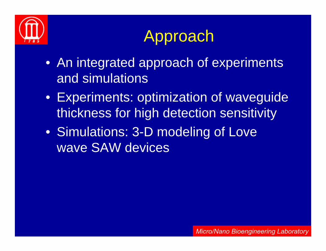
Approach• An integrated approach of experiments
and simulations• Experiments: optimization of waveguide
thickness for high detection sensitivity• Simulations: 3-D modeling of Love
wave SAW devices

Micro/Nano Bioengineering Laboratory
Experiments: SAW devices
Commercial two port SAW resonator Waveguide coating
Network analyzer
Port 1 Port 2
DUT
• Commercial SAW devices are coated with parylene in various thicknesses of 100 nm, 200 nm, 400 nm and 1 µm.• Changes in insertion loss and frequency shift are determined against a control case (without a parylene coating).
Change in waveguide thickness in a Love wave device

Micro/Nano Bioengineering Laboratory
• SAW sensors are coated, on top of the parylene waveguide layer, with a SAM of dithiobis succinimydyl propionate at various concentrations 0.5 mM. 0.75 mM, 1.0 mM, 2.5 mM, and 5.0 mM.
• Change in insertion loss and frequency shift are determined.
Experiments: SAW devices
Commercial two port SAW resonator
Waveguide coating
Network analyzer
Port 1 Port 2
DUT
Gold coating SAM adsorption
Detection of adsorption of SAM at various concentrations
Micro/Nano Bioengineering Laboratory
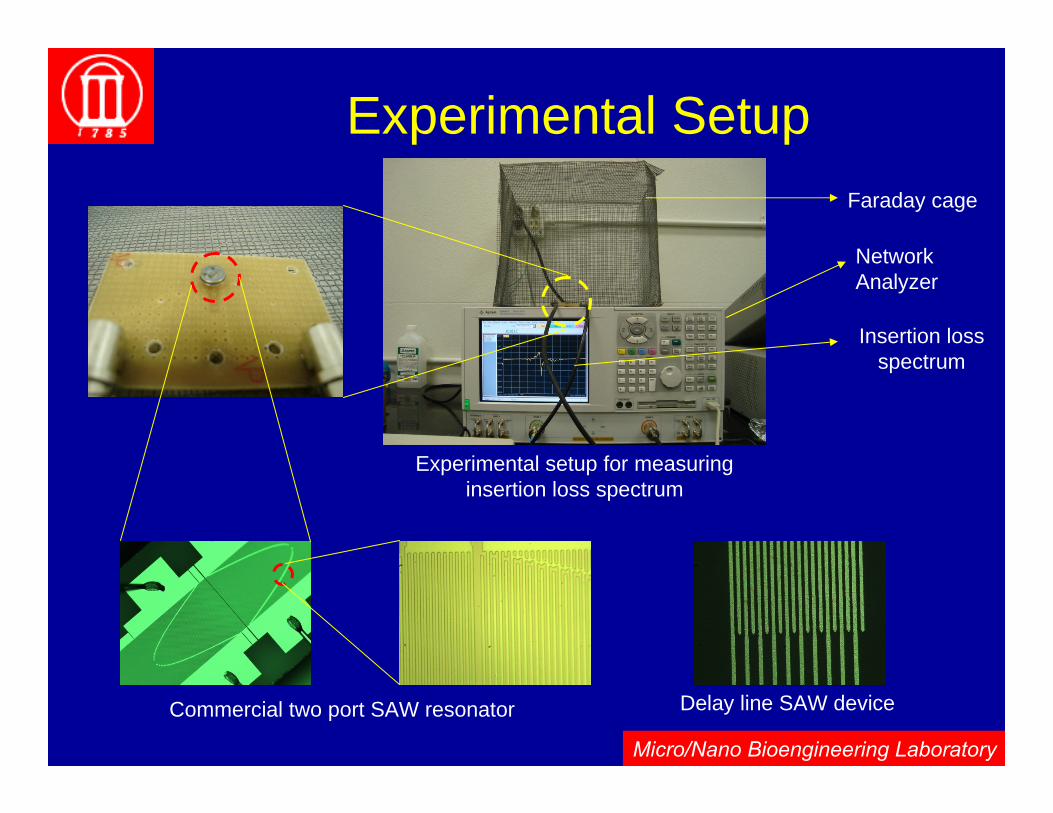
Experimental Setup
Experimental setup for measuring insertion loss spectrum
Insertion loss spectrum
Faraday cage
Network Analyzer
Commercial two port SAW resonator Delay line SAW device

Micro/Nano Bioengineering Laboratory
B
Results: waveguide thickness
Insertion loss spectra of a SAW sensor with and without a parylene coating.
A

Micro/Nano Bioengineering Laboratory
SAM detection sensitivity
Insertion loss spectra of a SAW sensor to SAM adsorption at 0.5 mM (A), 0.75 mM (B), 1.0 mM (C), 2.5 mM (D) and 5.0 mM (E) of SAM.

Micro/Nano Bioengineering Laboratory
Modeling: Love SAW devices
Piezoelectric substrate material YX Quartz
Frequency of operation 433.92 MHz
Wavelength 7.28µm
IDT finger width and spacing 1.82µm
Waveguide material Parylene
Waveguide dimensions 36.4µm x 14.56µm x 100nm
Piezoelectric substrate
Waveguide layer
36.4µm
14.56µm
Y
X
Z

Micro/Nano Bioengineering Laboratory
EeSCT tE •−•= ESeD s •+•= ε
( ) ⎟⎟⎟⎟⎟⎟⎟⎟
⎠
⎞
⎜⎜⎜⎜⎜⎜⎜⎜
⎝
⎛
−
−
−
=
2/00000000
0000000000
121114
1444
441414
331313
14131112
14131211
CCCCC
CCCCCC
CCCCCCCC
C
⎟⎟⎟
⎠
⎞
⎜⎜⎜
⎝
⎛=
33
11
11
000000
εε
εε
Elasticity Matrix for quartz
Dielectric Matrix for quartz
Governing Equations
⎟⎟⎟
⎠
⎞
⎜⎜⎜
⎝
⎛−
−=
000000
0000
333131
152222
2215
eeeeee
eee
Stress Matrix for quartz
Where T is the stress tensor, CE is the stiffness matrix, S the strain tensor, e the piezoelectric coupling tensor, E the electric field vector, d the electric displacement, ε the dielectric matrix, and the superscript t represents the transpose of a matrix.
YX Quartz
C11 8.674×10¹⁰ Nm-2
C12 0.699×10¹⁰ Nm-2
C13 1.191×10¹⁰ Nm-2
C14 -1.791×10¹⁰ Nm-2
C33 10.72×10¹⁰ Nm-2
C44 5.794×10¹⁰ Nm-2
E11 0.171 Cm-2
e14 0.0403 Cm-2
ε11 4.42
ε33 4.63
ρ 2650 Kg m-3
Parylene
E 0.4MPa
ν 0.40
ρ 1289 Kg m-3
Micro/Nano Bioengineering Laboratory
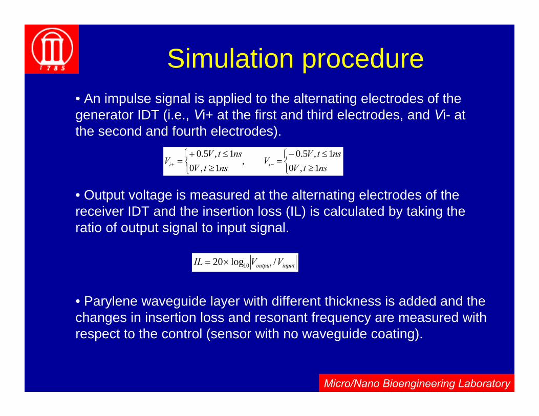
Simulation procedure• An impulse signal is applied to the alternating electrodes of the generator IDT (i.e., Vi+ at the first and third electrodes, and Vi- at the second and fourth electrodes).
⎩⎨⎧
≥≤−
=⎩⎨⎧
≥≤+
= −+ nstVnstV
VnstVnstV
V ii 1,01,5.0
,1,0
1,5.0
• Output voltage is measured at the alternating electrodes of thereceiver IDT and the insertion loss (IL) is calculated by taking the ratio of output signal to input signal.
inputoutput VVIL /log20 10×=
• Parylene waveguide layer with different thickness is added and the changes in insertion loss and resonant frequency are measured with respect to the control (sensor with no waveguide coating).

Micro/Nano Bioengineering Laboratory
BA
Snap shots of wave propagation at 2.3 ns (A) and at 3.3 ns (B).
Distance traveled = 7.35 µmTime taken = 2.3 nsCalculated wave velocity = 3152 m/sTheoretical wave velocity = 3159 m/s
Wavelength = 7.28 µm
Calculated frequency = 431.80 MHzTheoretical frequency = 432.96 MHz
Results: Wave propagation

Micro/Nano Bioengineering Laboratory

Micro/Nano Bioengineering Laboratory
Waveguide thickness
A
100nm
A
100nm
B
632.5nm
B
632.5nm
C
1.265µm
C
1.265µm
Snap shots of wave propagation in a Love wave SAW sensor with parylene coatings in a thickness of 100 nm (A), 632.5 nm (B) and 1.265 µm (C).
4waveguideh λ= mfV owwaveguide µλ 55.2==
Vw = 1100m/sec f0 = 431.318MHz nmh 5.637=
Theoretical determination of critical waveguide thickness
Where h is the thickness of the waveguide layer, λwaveguide is the wavelength of the waveguide, fo is the resonant frequency of the device, Vw is the wave velocity of waveguide layer

Micro/Nano Bioengineering Laboratory
Different SAW transducers
Tested commercial SAW device
Piezoelectric substrate
Waveguide layer
Simulated SAW device
Micro/Nano Bioengineering Laboratory
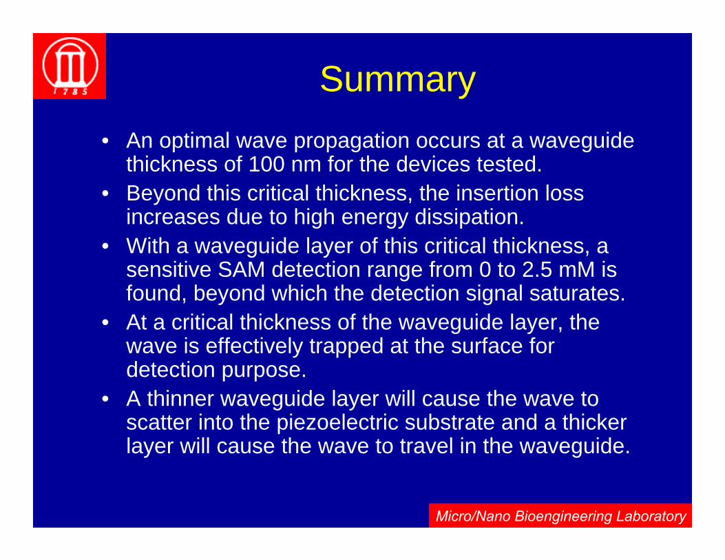
• An optimal wave propagation occurs at a waveguide thickness of 100 nm for the devices tested.
• Beyond this critical thickness, the insertion loss increases due to high energy dissipation.
• With a waveguide layer of this critical thickness, a sensitive SAM detection range from 0 to 2.5 mM is found, beyond which the detection signal saturates.
• At a critical thickness of the waveguide layer, the wave is effectively trapped at the surface for detection purpose.
• A thinner waveguide layer will cause the wave to scatter into the piezoelectric substrate and a thicker layer will cause the wave to travel in the waveguide.
Summary

Micro/Nano Bioengineering Laboratory
• To design a Love wave SAW sensor for bio-environment operation, it is essential to use a waveguide layer with a critical thickness.
• This critical thickness may vary depending on the actual layout of the SAW transducers.
Conclusions

Micro/Nano Bioengineering Laboratory
Acknowledgements
Thank you
National Science FoundationFaculty of Engineering
College of Agricultural and Environmental SciencesUniversity of Georgia