optical interconnections in digital systems—status and prospects
TRANSCRIPT
Optical interconnections in digital systems— Status and prospects
By D. Z. Tsang
In computing, trends toward parallel processing, multiprocessor computers, higher operating
speeds, and larger as well as denser very large scale integrated (VLSI) circuits have provided an impetus for the development of advanced interconnection technology. Multiprocessor computer designs tend to require both a larger number and a higher density of interconnections with a higher degree of connectivity than single-processor computers. The combination of higher operating speed, longer distances, and higher density leads to problems in maintaining signal integrity because of parasitic reactances, impedance mismatches, crosstalk, dispersion, and frequency-dependent skin effect losses. Also, as chip designs become larger and denser, the so-called pinout problem, in which the number of input/output pins and pads is limited by the density of wirebonds, is of increasing concern to VLSI circuit designers.
Optical interconnections have been of interest at all levels in digital computers for applications between mainframes, modules, boards,1 chips, 2 - 4
and even points within a chip. 5 They are viewed both as a technology to be used in conjunction with electrical interconnections and electronic logic circuits and as an enabling technology for optical computers. These interconnections are expected to provide advantages in situations that require high speed, high interconnection density, high connectivity, long distance, and the flexibility of optics. The
basic characteristics and advantages of optical interconnections, the current status of work in the field, and the prospective performance of optical interconnection systems are described here.
Present high-speed digital systems are limited by the packaging and electrical interconnection technology. 6 While the fastest transistors have switching times of the order of 10 ps, the fastest commercial integrated circuits (GaAs logic) are limited by package parasitics to rise and fall times of the order of 100 ps. Signal propagation within circuit boards results in some additional deterioration. The electrical backplane, into which boards are inserted, can only transfer rise times of 1 ns between boards. In effect, interconnection limitations restrict current clock cycle times to the order of 10 ns, although reduced times are promised in the next gener
ation of machines.
Optical interconnection configurations
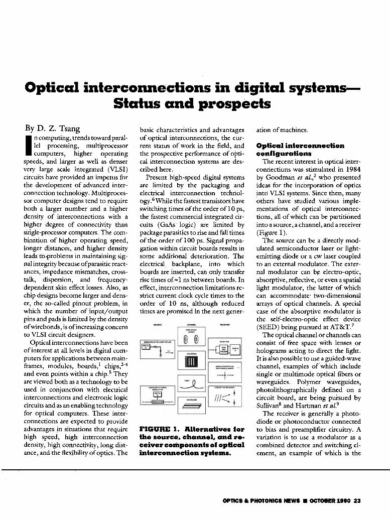
The recent interest in optical interconnections was stimulated in 1984 by Goodman et al.,2 who presented ideas for the incorporation of optics into VLS I systems. Since then, many others have studied various implementations of optical interconnections, all of which can be partitioned into a source, a channel, and a receiver (Figure 1).
The source can be a directly modulated semiconductor laser or light-emitting diode or a cw laser coupled to an external modulator. The external modulator can be electro-optic, absorptive, reflective, or even a spatial light modulator, the latter of which can accommodate two-dimensional arrays of optical channels. A special case of the absorptive modulator is the self-electro-optic effect device (SEED) being pursued at A T & T . 7
The optical channel or channels can consist of free space with lenses or holograms acting to direct the light. It is also possible to use a guided-wave channel, examples of which include single or multimode optical fibers or waveguides. Polymer waveguides, photolithographically defined on a circuit board, are being pursued by Sullivan 8 and Hartman et al.9
The receiver is generally a photodiode or photoconductor connected to bias and preamplifier circuitry. A variation is to use a modulator as a combined detector and switching element, an example of which is the
FIGURE 1. Alternatives for the source, channel, and receiver components of optical interconnection systems.
OPTICS & PHOTONICS NEWS • OCTOBER 1990 23

S E E D , or to include a wavelength-selective filter in front of the detector, as is under consideration at I B M ( A T & T and Bellcore are also pursuing this for other purposes).
In any of the combinations, one source is combined with one of the channels and one of the receivers to form the optical interconnection. The central idea behind all of the combinations is to minimize the length of electrical line, preferably a short wire, between the digital chip or driver and the source, so that the signal is converted to light before significant degradation. A similar argument applies to the receiver. For the single optical channel this has many advantages. Impedance matching, reflections, and ground planes should be less of a problem than with high-speed electrical interconnections. Loss is independent of length and dispersion is negligible for distances of interest. The optical channel itself has low crosstalk because photons do not interact, although stray light from scattering, reflection, or diffraction onto the detector can be an issue. The channel has high bandwidth, and with free-space interconnections, no physical contact is needed. The disadvantages include the cost of the sources and detectors and loss of signal due to limited opto-electronic conversion efficiency, and coupling and alignment problems.
Additional flexibility becomes apparent when considering multiple channels. With free-space channels, beams can cross with no interference and several channels can coexist in the same space. With guided-wave optics, waveguides can cross at an angle with little penalty. Holographic optical
channels promise a very high number and density ofinterconnections. Two-dimensional imaging techniques can be applied for arrays of highly parallel interconnections. In addition, many researchers are studying techniques for reconfigurable optical interconnections in which the computer architecture can be optimized for specific problems. 2 , 1 0 Other researchers are studying computer architectures in which an optical implementation would be far easier to construct than its electrical counterpart.
The optical channel has received most of the attention from researchers, but the entire system and the system performance must be considered. Conversion or modulation efficiency of the optical source, coupling and alignment, overall link efficiency, and interfaces to the digital world must be considered. The eventual cost of each link will be very important because, conservatively estimated, a single computer may have 100-100,000 links. Packaging and reliability of a system will also be crucial to the acceptance of optical interconnections, as will the need for bit error rates ranging from 10-12 to 1 0 - 1 5 .
Experimental optical interconnection systems
Several experimental optical interconnections between digital circuits have been demonstrated. For example, fiber-optic interconnections have been installed in a multiprocessor computer by Lane and coworkers 1 1 in a collaborative effort between Honeywell and Thinking Machines. Using only commercially available transmitters and receivers, as well as proven GaAs digital multiplexers and demul
tiplexers, these researchers replaced 1024 wires by two optical fibers to form one leg of a hypercube architecture. Successful computer operation was demonstrated with the optical links operating at400 M b / s , and further work toward 1 G b / s is in progress.
Components for optical links in computers have been developed and demonstrated at I B M . 1 2 A four-channel GaAs laser driver was connected to a four-element graded- index separate-confinement heterostructure single quantum well laser array with hybrid integration techniques. Four optical fibers were aligned in an array of V grooves and polished to reflect the light onto four interdigitated Schottky photodiodes. The photodiodes were monolithically integrated with a M E S F E T receiver. The high level of integration (2000 devices in the receiver) will be important to the further development of many parallel channels.
Presently, electrical interconnec-
FIGURE 2. Illustration of free-space optical interconnections between boards, showing signal transmission by laser beams in direct paths.
24 OPTICS & PHOTONICS NEWS • OCTOBER 1990
tions are arranged in two-dimensional planes, in chips, on boards, and in backplanes. For board-to-board communication, a signal from a chip must be sent to the edge of the board, through a (often slow) backplane, and then from the edge of the next board to the desired position on the board. With an optical interconnection, the signal can be transmitted over a light beam from one board to the next, as shown in Fig. 2, without physical contact between boards. Interconnections can be located anywhere on the board, not just at one or two edges, which could add a third dimension to the layout of logic systems.
Currently, a 1-Gb/s fiber-optic telecommunication transmitter module and its corresponding receiver are expensive, each costing several thousand dollars. However, the interconnection problem is different from the long-distance telephone problem. The short distance and the small attenuation, combined with very efficient lasers and detectors, can minimize the driver and receiver circuitry required for the interconnection and thereby reduce its cost.
High-speed optical fiber communication systems designed for long-distance transmission typically have an overall electrical differential current efficiency, differential current out of the detector divided by differential current into the laser when both are biased at the operating point, of 1 to 3% for short links. Attenuation in a long fiber will reduce the efficiency even further. Consequently, when components designed for long-distance fiber systems are employed in a short-distance optical interconnection, only 1-3% of the current into the laser
is delivered by the detector. Since all interconnections must deliver the same standardized voltage level for compatibility with conventional digital logic, the detected signal requires amplification to recover the logic level.
There are three fundamental contributions to the overall efficiency. For a laser biased at or above threshold, the differential current efficiency of a link is proportional to the product of the laser differential quantum efficiency, the detector quantum efficiency, and
the optical system efficiency, where the optical system efficiency is defined as the fraction of the photons emitted by the laser that are incident on the detector. Because the electrical power out of the detector is proportional to the square of the detector current, the electrical output power varies as the square of the quantum efficiencies. Thus, efficient devices are very important. The need to maintain high optical system efficiency dictates the use of lenses or holograms for free-space interconnections to ensure that a large fraction of the emitted photons arrives on the desired detectors. With an efficient optical interconnection, much of the interface circuitry required by inefficient systems (laser driver, preamplifier, automatic gain control, timing recovery, etc.) can be eliminated. Costs, power consumption, and the need for high-gain amplifiers—best avoided in a digital environment with nearby logic gates switching on and off—are reduced.
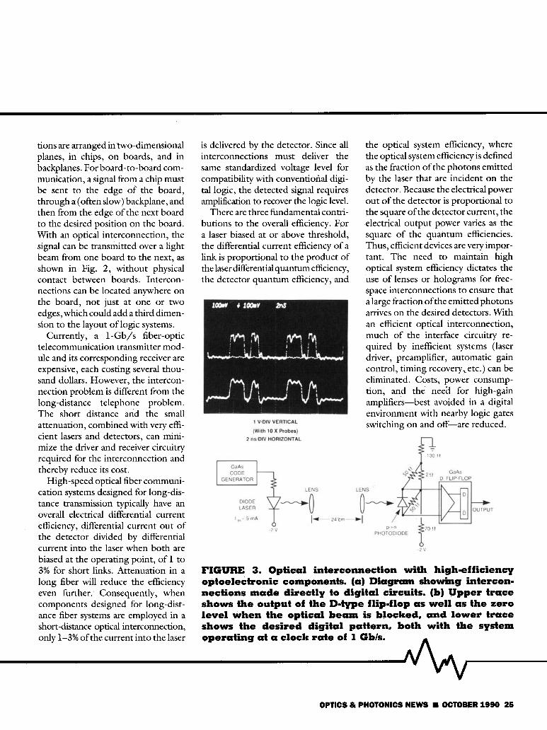
FIGURE 3. Optical interconnection with high-efficiency optoelectronic components. (a) Diagram showing interconnections made directly to digital circuits. (b) Upper trace shows the output of the D-type flip-flop as well as the zero level when the optical beam is blocked, and lower trace shows the desired digital pattern, both with the system operating at a clock rate of 1 Gb/s.
OPTICS & PHOTONICS NEWS • OCTOBER 1990 25

Our effort 1 3 has been aimed at implementing an optical interconnection between digital gates without the use of a complicated fiber-optic type transmitter and receiver. Shown in Fig, 3(a) is an optical interconnection that was made by connecting a diode laser directly to one digital circuit on one board, and a detector directly to another circuit on another board. The voltage levels of the GaAs integrated circuits were compatible with emitter-coupled logic (ECL) . A diode laser was chosen over a light-emitting diode because of its inherent higher efficiency, its narrower emission cone, and its higher speed. A 1.3-mm GaInAsP laser 1 4 was connected to a GaAs code generator that produces a fixed word sequence. The laser threshold is 5 mA and the external differential quantum efficiency is 35% per facet. The low threshold allows the interconnection to be driven directly by logic gates, while the high differential efficiency allows the detector to generate signal levels sufficiently high to be connected directly to another digital gate without the need for preamplification.
The laser light is collected and collimated by an inexpensive aspheric compact-disc lens of 0.55 numerical aperture and 5 mm diameter. The light travels 24 cm, many times the distance required for typical board-to-board applications, to an identical lens that focuses the light onto a commercially available 100-µm-diameter GaInAs p-i-n photodiode with a nominal 70% quantum efficiency. The output of the photodiode is connected directly to the input of another GaAs digital circuit—a D-type flip-flop-which, as shown in Fig. 3(a), has an
internal amplifier or comparator. In another experiment with a laser with a differential efficiency of 30% per facet, an overall differential electrical current efficiency of 12.5% was measured. This is much better than the 1-3% efficiency common in high
speed fiber-optic systems. Even higher differential current efficiencies of 19% were measured with a laser having a differential efficiency of 61% per facet.
The D-type flip-flop regenerates the digital output at rates from 100 M b / s up to 1 G b / s [Fig. 3(b)], the limit of the GaAs code generator. N o external laser drivers or preamplifiers are required. This demonstrates that with efficient opto-electronic components, digital circuits can be interconnected simply and directly. The interconnection in Fig. 3(a) has the potential for a fanout of two, since the light from the back facet could also be collected and sent to another gate. The power consumption of the final stage in the GaAs digital circuit and the diode laser is estimated to be 2 0 -25 mW for a bit pattern with an equal probability of ones and zeros. The resistor network interface between the photodiode and the gate input serves to supply any input bias current to the gate as well as to provide an interface to the photodiode, but is probably not optimal and dissipates about 20 mW with 2 mA of photocurrent.
In our present setup, the transmitter and receiver boards are positioned with micropositioner stages, and both the lenses and stages are mounted on an optical table. This is not practical for electronic systems. Eventually, we want to incorporate the lens within a module and eliminate the optical translation stages. Then, the question will be whether the dependence of the performance on the mechanical alignment tolerances will prove practical.
Prospective performance The evolution of optical intercon-
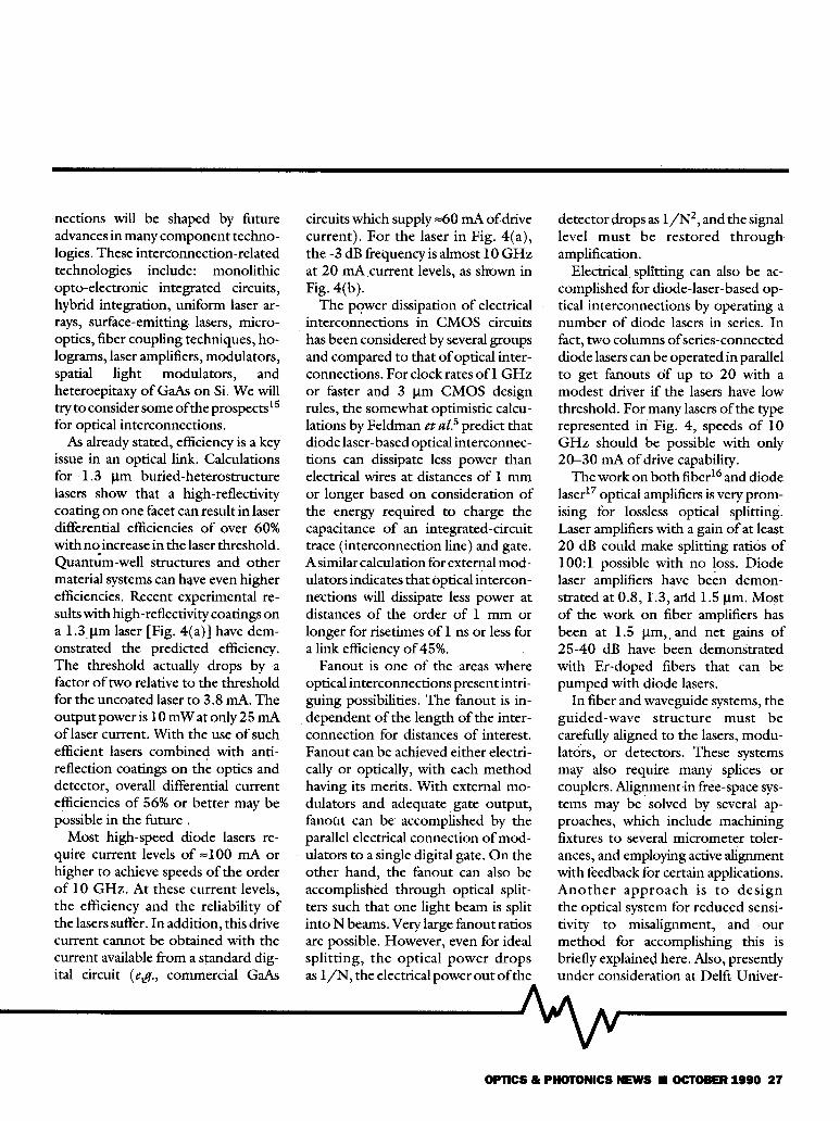
FIGURE 4. Diode laser with high-reflectivity coating. (a) Improvement of single-ended external differential quantum efficiency after coating. (b) -3 dB frequency as a function of drive level. The actual drive current is indicated at each point.
26 OPTICS & PHOTONICS NEWS • OCTOBER 1990
nections will be shaped by future advances in many component technologies. These interconnection-related technologies include: monolithic opto-electronic integrated circuits, hybrid integration, uniform laser arrays, surface-emitting lasers, micro-optics, fiber coupling techniques, holograms, laser amplifiers, modulators, spatial light modulators, and heteroepitaxy of GaAs on Si. We will try to consider some of the prospects 1 5
for optical interconnections. As already stated, efficiency is a key
issue in an optical link. Calculations for 1.3 µm buried-heterostructure lasers show that a high-reflectivity coating on one facet can result in laser differential efficiencies of over 60% with no increase in the laser threshold. Quantum-well structures and other material systems can have even higher efficiencies. Recent experimental results with high-reflectivity coatings on a 1.3 µm laser [Fig. 4(a)] have demonstrated the predicted efficiency. The threshold actually drops by a factor of two relative to the threshold for the uncoated laser to 3.8 mA. The output power is 10 mW at only 25 mA of laser current. With the use of such efficient lasers combined with anti-reflection coatings on the optics and detector, overall differential current efficiencies of 56% or better may be possible in the future .
Most high-speed diode lasers require current levels of 100 mA or higher to achieve speeds of the order of 10 G H z . A t these current levels, the efficiency and the reliability of the lasers suffer. In addition, this drive current cannot be obtained with the current available from a standard digital circuit (e.g., commercial GaAs
circuits which supply 60 mA of drive current). For the laser in F ig . 4(a), the -3 dB frequency is almost 10 G H z at 20 mA current levels, as shown in Fig. 4(b).
The power dissipation of electrical interconnections in C M O S circuits has been considered by several groups and compared to that of optical interconnections. For clock rates of 1 G H z or faster and 3 µm C M O S design rules, the somewhat optimistic calculations by Feldman et al.5 predict that diode laser-based optical interconnections can dissipate less power than electrical wires at distances of 1 mm or longer based on consideration of the energy required to charge the capacitance of an integrated-circuit trace (interconnection line) and gate. A similar calculation for external modulators indicates that optical interconnections will dissipate less power at distances of the order of 1 mm or longer for risetimes of 1 ns or less for a link efficiency of 45%.
Fanout is one of the areas where optical interconnections present intriguing possibilities. The fanout is independent of the length of the interconnection for distances of interest. Fanout can be achieved either electrically or optically, with each method having its merits. With external modulators and adequate gate output, fanout can be accomplished by the parallel electrical connection of modulators to a single digital gate. O n the other hand, the fanout can also be accomplished through optical splitters such that one light beam is split into N beams. Very large fanout ratios are possible. However, even for ideal spli t t ing, the optical power drops as 1 / N , the electrical power out of the
detector drops as 1 / N 2 , and the signal level must be restored through amplification.
Electrical splitting can also be accomplished for diode-laser-based optical interconnections by operating a number of diode lasers in series. In fact, two columns of series-connected diode lasers can be operated in parallel to get fanouts of up to 20 with a modest driver i f the lasers have low threshold. For many lasers of the type represented in Fig. 4, speeds of 10 G H z should be possible with only 20-30 mA of drive capability.
The work on both fiber16 and diode laser 1 7 optical amplifiers is very promising for lossless optical splitting. Laser amplifiers with a gain of at least 20 dB could make splitting ratios of 100:1 possible with no loss. Diode laser amplifiers have been demonstrated at 0.8, 1.3, arid 1.5 µm. Most of the work on fiber amplifiers has been at 1.5 µm, and net gains of 25-40 dB have been demonstrated with Er-doped fibers that can be pumped with diode lasers.
In fiber and waveguide systems, the guided-wave structure must be carefully aligned to the lasers, modulators, or detectors. These systems may also require many splices or couplers. Alignment in free-space systems may be solved by several approaches, which include machining fixtures to several micrometer tolerances, and employing active alignment with feedback for certain applications. A n o t h e r approach is to des ign the optical system for reduced sensitivity to misalignment, and our method for accomplishing this is briefly explained here. Also, presently under consideration at Delft Univer
OPTICS & PHOTONICS NEWS • OCTOBER 1990 27

sity 1 8 are alignment invariant designs, in which software determines the pixels that are interconnected for any given alignment.
The use of optical modules containing a source or detector for each interconnection together with prealigned optics can greatly simplify the alignment problems. 1 9 The optics of the transmitter module allow the laser beam to expand to a size consistent with circuit board tolerances, and the optics in the receiver module serve to focus the expanded beam onto a detector. A l l critical alignments between the lens and the source or detector are performed during module assembly. During circuit assembly, the modules need only be aligned to the much less critical (approximately millimeter) tolerances of the expanded-beam input/output optics. For low insertion loss in the optical link, the receiver lens must be located in the near field of the transmitter lens, so that most of the signal can be collected. The effects of misalignment have been considered one at a time19
using simplified thin-lens approximations of the optics and a uniform distribution of light. For a board-to-board interconnection with a transmitter graded-index (GRIN) lens of 1 mm diameter and a receiver G R I N lens of 2 mm diameter, 0,7-mm lateral misalignment or 2-degree misalignment of either the transmitter or the receiver is consistent with an optical system efficiency of 80% and rise times of 50 ps for a board separation of 3 cm.
Very high densities of interconnections are possible with optical interconnections. Two-dimensional planes of interconnections can be easily im
aged with optics. Over a million vertical cavity surface-emitting lasers per square centimeter have been fabricated by Jewell et al.20 although operation at this density has not been demonstrated. Improvements in thermal dissipation and in the series resistance of such devices can lead to a wide range of applications, including interconnections.
The role of optics The areas where optical and electri
cal interconnections should be important are shown in Fig. 5. A t low speeds and short distances (lower left region of the figure), simple wires will predominate because they are cheap and effective. Possible reasons to consider optics in this region are to overcome the difficulties associated with physical layouts, crosstalk, or when implementing high-density or high-connectivity interconnections. As frequencies and distances increase, crosstalk is more of a problem and the reactance (capacitive or inductive) of a wire begins to cause signal distortion. The line corresponding to an inductive impedance of 5 Ω for a 25 mil diameter wire is a rough indication of where other interconnection techniques may be considered. This inductance is that of a 50 µm-diameter wire. Depending on the impedances and current-handling capabilities of the digital circuits and the geometry, size, and resistance of the wire (e.g., C M O S versus E C L circuits, flat versus round wires, etc.), wires may have limitations to the lower left of the 5-W line, or remain useful to the upper right of the line. The physical limit on the use of a wire, even a superconducting wire, occurs when the length of
the interconnection approaches the wavelength of the signal being transmitted. A n approximate limit is shown in Fig. 5 by the solid line that indicates a λ/10-long interconnection.
When unacceptable distortion or crosstalk results from the use of simple wires, alternative interconnection technologies, electro-magnetic transmission lines, and optics, must be employed. Transmission lines include twisted pair, microstrip, stripline, and coax. Transmission lines become dispersive and suffer losses from the skin effect as the speed increases. The approximate limit for the use of transmission-line techniques is shown in Fig. 5 by the line for a 3-mm-diameter 77-coax copper airline at room temperature. The sloped portion of the line corresponds to a 3 dB propagation loss while the horizontal portion
FIGURE 5. Regions of interest for electrical and optical interconnections based on both speed and distance.
28 OPTICS & PHOTONICS NEWS • OCTOBER 1990
is at the frequency where higher-order modes become important. Superconductors may extend these limits.
The region where optical interconnection techniques begin to promise advantages in terms of power, isolation, and signal distortion begins roughly at the boundary where wires begin to have difficulties. There exists a large and currently important range of speed and interconnection distance over which optical and transmission-line techniques are of interest, and the unique features of each may be used depending on the application. A t high speeds and long distances, optical interconnections offer the best solution because of the bandwidth and low loss of both optical fibers and free space. The high bandwidth of present optical channels allows signal transmission above 1 0 1 1 H z , although appropriate sources and receivers have yet to be developed.
In summary, various types of optical interconnections have been demonstrated in the laboratory and in commercial computers. Optical interconnections have prospects for even better performance with improved concepts, devices, and systems and should facilitate the development of advanced computers. The challenges ahead are to develop the potential of optical interconnections in the laboratory, to transfer the technology into the computer environment, and to make the technology cost effective.
Acknowledgments The author would like to thank R.
C . Williamson and D. L. Spears for helpful discussions and M . J . Corcoran for technical assistance. This work was sponsored by the Defense A d
vanced Research Projects Agency.
R E F E R E N C E S 1. W. T. Cathey and B.J . Smith, High concurrency
data bus using arrays of optical emitters and detectors, Appl. Opt. 18, 1979. p.1687.
2. J. W. Goodman, F. J. Leonberger, S.-Y. Kung, and R. A. Athale, Optical interconnections for VLSI systems, Proc. IEEE 72, 1984. p. 850.
3. R. K. Kostuk, J. W. Goodman, and L. Hesselink, Optical imaging applied to microelectronic chip-to-chip interconnection, Appl. Opt. 24, 1985. p. 2851.
4. W. H. Wu, L. A. Bergman, A. R. Johnston, C. C. Guest, S. C. Esener, P. K. L. Yu, M. R. Feldman, and S. H. Lee, Implementation of optical interconnections for VLSI, IEEE Trans. Electron Devices ED-34, 1987. p. 706.
5. M. R. Feldman, S. C. Esener, C. C. Guest, and S. H. Lee, Comparison between optical and electrical interconnects based on power and speed considerations, Appl. Opt. 27, 1988. p. 1742.
6. This point has also been made by Alan Huang and Ron Reedy.
7. A. L. Lentine, H. S. Hinton, D. A. B. Miller, J. E. Henry, J. E. Cunningham, L. M. F. Chirovsky, Symmetric self-electro-optic effect device: optical set-reset latch, Appl. Phys. Lett. 52, 1988. p. 1419.
8. C. T. Sullivan, Optical waveguide circuits for printed wire-board interconnections, Proc. SPIE 994, 1988. p. 92.
9. D. H . Hartman, G. R. Lalk, J. W. Howse, and R. R. Krchnavek, Radiant cured polymer optical waveguides on printed circuit boards for photonic interconnection use, Appl. Opt. 28, 1989. p. 40.
10. See for example P. Yeh, A. E. T. Chiou, J. Hong, Optical interconnection using photorefractive dynamic holograms, Appl. Opt. 27, 1988. p. 2093.
11. T. A. Lane, J. A. Quam, B. O. Kahle, and E. C. Parish, Gigabit optical interconnects for the Connection Machine, Proc. SPIE 1178, 1989. p. 24.
12. J. D. Crow, Fiber-optic modules for high speed computer networks, 1989 Proc. 39th Electronic Components Conference, IEEE, New York, 1989. p. 355.
13. D. Z. Tsang, One-gigabit per second free-space optical interconnection, Appl. Opt. 29, 1990. p. 2034.
14. D. Z. Tsang and Z. L. Liau, Sinusoidal and digital high speed modulation of p-type substrate mass-transported diode lasers, J. Lightwave Technol. LT-5, 1987. p. 300.
15. The interested reader is referred to Applied Optics 29 (1990) for recent feature issues on optical interconnections (pp. 1067-1161) and optical computing (pp. 1999-2187).
16. P. Urquhart, Review of rare earth doped fibre
lasers and amplifiers, IEEE Proc. 125, Pt. I,1988. p. 385.
17. T. Saitoh and T. Mukai, Recent progress in semiconductor laser amplifiers, J. Lightwave Technol. 6, 1988. p. 1656.
18. E. E. Freitman, private communication. 19. D. Z. Tsang, Alignment and performance trade
offs for free-space optical interconnections, 1989 Technical Digest Series, vol. 9 (Optical Society of America, Washington, D.C., 1989), p. 146.
20. J. L. Jewell, Y. H. Lee, A. Scherer, S. L. McCall, N. A. Olsson, J. P. Harbison, and L. T. Florez, Surface-emitting microlasers for photonic switch -ing and interchip connections, Opt. Eng. 29, 1990. p. 210.
D E A N T S A N G is a staff member in the Applied Physics Group at M I T ' s L in coln Laboratory.
OPTICS & PHOTONICS NEWS • OCTOBER 1990 29