optical efficiency in image sensor pixels
TRANSCRIPT

7/30/2019 Optical Efficiency in Image Sensor pixels
http://slidepdf.com/reader/full/optical-efficiency-in-image-sensor-pixels 1/11
Optical efficiency of image sensor pixels
Peter B. Catrysse and Brian A. Wandell
Department of Electrical Engineering, Stanford University, Stanford, California 94305
Received November 19, 2001; accepted January 31, 2002
The ability to reproduce a high-quality image depends strongly on the image sensor light sensitivity. Thissensitivity depends, in turn, on the materials, the circuitry, and the optical properties of the pixel. We calcu-late the optical efficiency of a complementary metal oxide semiconductor (CMOS) image sensor pixel by using a geometrical-optics phase-space approach. We compare the theoretical predictions with measurements madeby using a CMOS digital pixel sensor, and we find them to be in agreement within 3%. Finally, we show howto use these optical efficiency calculations to trade off image sensor pixel sensitivity and functionality as CMOSprocess technology scales. © 2002 Optical Society of America
OCIS codes: 040.5160, 040.6040, 080.2720, 110.2970.
1. INTRODUCTION
The ability to reproduce a high-quality image depends
strongly on the light sensitivity of an image sensor. Twofactors significantly influence light sensitivity. First, thematerials (process technology) and the devices (photode-tector type) that convert photons to electrons within eachimage sensor pixel set a limit on light sensitivity. Sec-ond, the light sensitivity depends on the geometric ar-rangement of the photodetector within an image sensorpixel and the pixel location with respect to the imaging optics. The former leads to quantum efficiency (QE), andthe latter can be summarized as optical efficiency (OE).
An important figure of merit for an image sensor is theexternal QE of its pixels. External QE measures thefraction of the incident photon flux that contributes to thephotocurrent in the pixel as a function of wavelength; itcomprises both QE and OE. Because of its complex de-pendency on materials and devices, external QE is typi-cally obtained experimentally.1–3 It is a global figure of merit and gives no detailed information about the nature,i.e., quantum or optical, of an efficiency bottleneck withinthe pixel. It is possible to characterize the photodetectorin a pixel by an internal QE, for which theoretical modelsexist.4 Unfortunately, most model assumptions breakdown for the small photodetectors integrated within typi-cal image sensor pixels. In this paper, however, we willfocus on the OE of an image sensor pixel and not elabo-rate on its internal QE.
Before the photon flux incident on a pixel is converted
into a photocurrent, it has to reach the photodetector.We define OE as the photon-to-photon efficiency from thepixel surface to the photodetector. Figure 1 is a scanning electron microscope image of a complementary metal ox-ide semiconductor (CMOS) image sensor pixel.5 The im-age shows a cross section through the pixel; light is inci-dent on the pixel surface, enters at the aperture, passesthrough several dielectric layers forming a tunnel, and isabsorbed by a photodetector on the pixel floor. The geo-metric arrangement of the photodetector with respect toother elements of the pixel structure, i.e., shape and sizeof the aperture, length of the dielectric tunnel, and posi-
tion, shape, and size of the photodetector, all determineOE. Experimental evidence shows that OE can be a sig-
nificant factor when an image sensor pixel is imple-mented by using either charge-coupled-device (CCD) orCMOS technology.6,7 Nevertheless, the OE of image sen-sor pixels has not been separately analyzed within a com-prehensive optical framework. Several commercial ray-trace programs include useful simulations that permitinferences about OE.8,9 These programs rely mainly onbrute force calculations, which in most cases have notbeen validated with the use of appropriate pixel teststructures. There is one published description of three-dimensional (3D) CCD modeling, but this study does notpresent an experimental validation.10
In this paper, we develop a theoretical basis for OE cal-culations by using a geometrical-optics phase-space (PS)
approach, and we provide a graphical method of deriving the OE of image sensor pixels. We make specific predic-tions for the CMOS image sensor pixel shown in Fig. 1,and we validate our model by using experimental mea-surements. We then extend the predictions for pixelsimplemented in future CMOS process technologies. Theremainder of the paper is organized as follows. In Sec-tion 2, we introduce the PS approach and show how it ap-plies to optical signals and systems. In Section 3, we cal-culate the OE of an imaging system consisting of a lensand an image sensor. In Sections 4 and 5, the experi-mental measurements are described and compared withthe theoretical PS predictions. In Section 6, we showhow to use these OE calculations to trade off pixel sensi-
tivity and functionality as CMOS process technologyscales.
2. THEORETICAL BACKGROUNDA. Geometrical-Optics Phase SpaceHamilton introduced the PS approach to light propaga-tion in geometrical optics.11 Winston further developedthis approach by introducing PS representations to studylight collection.12 We extend Winston’s results in twoways. The initial use of PS representations was to de-scribe optical signals. Here we show that it is possible touse PS representations to describe optical systems as
1610 J. Opt. Soc. Am. A /Vol. 19, No. 8 /August 2002 P. B. Catrysse and B. A. Wandell
0740-3232/2002/081610-11$15.00 © 2002 Optical Society of America

7/30/2019 Optical Efficiency in Image Sensor pixels
http://slidepdf.com/reader/full/optical-efficiency-in-image-sensor-pixels 2/11
well. Second, we show how to combine the signal andsystem PS representations, predict the system responsefrom the signal–system PS, and determine the systemOE.
Geometrical-optics PS representations consist of a four-dimensional (4D) function whose entries describe the re-lationship between each geometrical light ray and aplane, which is typically perpendicular to the optical axis.Two of the four dimensions define the location of the rayintersection with the plane, ( x , y); the other two dimen-sions describe the angles between the ray and the opticalaxis at the intersection point, ( x , y). In thegeometrical-optics PS representation, these angles areusually measured in terms of ( p, q), given by
p ϭ n sin x , q ϭ n sin y , (1)
where n is the index of refraction of the material at the
plane. We call ( p, q) ‘‘generalized reduced angles,’’ be-cause they are a nonparaxial generalization of the re-duced angles defined by Goodman.13 The spatial dimen-sions ( x, y) are unbounded; the angular dimensions( p , q) fall within a range of Ϫn to n: i.e., the PS repre-sentation is limited to forward-propagating rays.
Two-dimensional (2D) signals and systems u( x, y),such as imaging systems, have 4D PS representationsW ( x, y , p, q). In certain cases, the 4D representationcan be reduced to a 2D PS representations, W ( x, p).This dimensionality reduction is possible whenever the2D system can be represented by a simpler one-
dimensional (1D) system, for example in the case of rota-tional symmetry. In this case, the position along one spa-tial dimension x 0 and one angle 0 are enough tocharacterize each light ray. Figure 2 shows the 2D PSrepresentation of a geometrical ray: a point ( x0 , p0) inPS, where the generalized reduced angle is p0
ϭ n sin 0 . To provide an intuitive explanation of PSrepresentations and their use in determining pixel OE,we will rely on 1D signals and systems u( x) and a 2D PS
representations, W ( x, p). The geometrical-optics PhaseSpace Toolbox that we have developed uses the general4D representation W ( x, y, p , q).
In general, the relationship between a 1D signal or sys-tem u( x) and its 2D PS representation is obtained by theWigner transform14,15:
W x , ϭ ͵ u x ϩ xЈ /2 u * x Ϫ xЈ /2 exp Ϫ2 i x Ј d xЈ.
(2)
The Wigner transform from u( x) to W ( x, ) is reversibleup to a constant phase factor:
͵W x /2, exp 2 i x d ϭ u x u
* 0 ,
u 0 2ϭ ͵ W 0, d . (3)
We now define geometrical-optics PS as a binary functionof two variables,
W geom x, p ϭ 1 W x, Ͼ W thresh
0 otherwise, (4)
using a threshold value W thresh , and we relate the spatialfrequency ϭ (n sin )/ to the generalized reduced angle
p by
p ϭ . (5)
In what follows, we replace the subscript ‘‘geom’’ in or-der to distinguish between PS representations of opticalsignals, W I ( x , p), and of optical systems, W Y ( x, p).
1. Phase-Space Representation of SignalsConsider the PS representations W I ( x, p) of some funda-mental optical signals that can be used as input to an im-age sensor. A single ray of unit radiance is described by aposition x 0 and a direction p0 ϭ n sin 0 . We can use theDirac ␦ to represent the signal as (cf. Fig. 2)
Fig. 1. Scanning electron microscope image of a CMOS imagesensor pixel. The image shows a cross section. The white ar-eas show the metal layers and the connection vias. The topwhite layer is a dielectric passivation layer (Si3N4) sitting on topof a metal light shield. The shield has a square aperture so thatincident light can reach the photodetector. The photodetector(Si) is located at the bottom of a dielectric tunnel (SiO 2) of width5.5 m and depth 7.08 m.
Fig. 2. Geometrical-optics PS: The parameters ( x0 , p 0) definea geometrical ray incident on a surface in (a) one-dimensionalreal space and (b) two-dimensional phase space.
P. B. Catrysse and B. A. Wandell Vol. 19, No. 8 /August 2002 /J. Opt. Soc. Am. A 1611

7/30/2019 Optical Efficiency in Image Sensor pixels
http://slidepdf.com/reader/full/optical-efficiency-in-image-sensor-pixels 3/11
W I x , p ϭ ␦ x Ϫ x0 , p Ϫ p 0 ϭ ␦ x Ϫ x 0 ␦ p Ϫ p 0 .(6)
A plane wave of unit radiance has a single direction of propagation, p0 ϭ n sin 0 , and extends infinitely acrossspace. A horizontal line represents the plane wave in PS[Fig. 3(a)]:
W I x, p ϭ ␦ p Ϫ p 0 . (7)
A point source exists at a single position x 0 in space and
emits light in all directions. A vertical line representsthe point source in PS [Fig. 3(b)]:
W I x , p ϭ ␦ x Ϫ x 0 . (8)
An incoherent area source can consist of the image pro-duced by a lens filled with light16 centered on the spatialaxis x 0 in position. The rays are confined in space by thefinite diameter of the lens field stop, ⌬, and confined inangle by the lens numerical aperture (NA). A closed arearepresents the area source in PS [Fig. 3(c)]:
W I x, p ϭ ⌸ x Ϫ x 0
⌬,
p Ϫ p0
2NA
ϭ ⌸ x Ϫ x
0
⌬ ⌸ p Ϫ p
0
2NA . (9)
We define ⌸ as the rectangle function17:
⌸ x Ϫ x 0
⌬ x0 ϭ 1, x0 Ϫ
⌬ x0
2р x р x0 ϩ
⌬ x0
2
0, else
.
(10)
Finally, the photon flux of the optical signal is the integralof the geometrical-optics PS representation:
⌽ ϭ ͵͵ W I x , p d xd p. (11)
2. Phase-Space Representation of SystemsPS representations can also be used to describe the accep-tance range of signals incident on an optical system. Wedenote these system representations by W Y ( x, p) . Herethe axes are unchanged from the signal diagram, but the
value assigned to each location in the representation de-fines the system’s relative responsivity to a ray at that po-sition and angle. In many applications, it is sufficient tosummarize this responsivity by using a binary value, inwhich we treat each ray as falling either in or out of thesystem’s acceptance range:
W Y x, p ϭ 1 within acceptance range
0 else. (12)
The system’s responsivity can now be described graphi-cally by using shaded PS graphs (Fig. 4). As an imaging sensor example, consider the PS representation for a pixelwith a surface photodetector located at the pixel apertureplane. Figure 4(a) shows that the horizontal axis of the
PS representation spans the pixel width w and that the vertical axis spans the full hemisphere 2 n :
W Y x, p ϭ ⌸x
w⌸
p
2n. (13)
If the photodetector spans only half of the pixel aperture,w /2, the shaded region shrinks accordingly, as shown inFig. 4(b):
W Y x, p ϭ ⌸x
w /2⌸
p
2n. (14)
Finally, consider the PS representation of an on-axis pixelat the image plane of a lens [Fig. 4(c)]. The PS represen-tation of the lens–pixel system at the pixel aperture planedepends jointly on the lens and the pixel PS representa-tions [Fig. 4(b)]. The PS representation of the system isnecessarily the intersection of the two PS representa-tions. On the horizontal axis, the PS of the lens spansthe width of the field stop, ⌬; the pixel is bounded by thewidth w /2 of the photodetector. On the vertical axis, thepixel accepts a full hemisphere; the lens, however, isbounded by its NA:
W Y x, p ϭ ⌸x
w /2⌸
p
2NA . (15)
Fig. 3. PS representation of optical signals: (a) plane wave, (b)point source, (c) area source.
Fig. 4. PS representations of several surface photodetector con-figurations: (a) photodetector covering the entire pixel area(100% fill factor), (b) photodetector covering half of the pixel area(50% fill factor), (c) photodetector covering half of the pixel areaplaced on axis in the imaging plane of a lens. The light-shadedarea represents the PS representation of the lens at the imageplane, and the black rectangle indicates the intersection of thesurface photodetector PS and the lens PS.
1612 J. Opt. Soc. Am. A /Vol. 19, No. 8 /August 2002 P. B. Catrysse and B. A. Wandell

7/30/2019 Optical Efficiency in Image Sensor pixels
http://slidepdf.com/reader/full/optical-efficiency-in-image-sensor-pixels 4/11
The integral of the geometrical-optics PS representationmeasures the geometric etendue G, i.e., the maximum in-cident photon flux transmittable by the optical system18:
G ϭ ͵͵ W Y x, p d xd p . (16)
Geometric etendue G is the energetic equivalent of the op-tical space–bandwidth product described in Lohmann
et al.19 It is a limiting function of system throughputand is determined by the least-optimized segment of theentire system. We now derive the geometric etendue G
for the example image sensor systems in Fig. 4. For apixel with a surface photodetector spanning the entirepixel width w in a medium with refractive index n, theetendue is G ϭ 2nw . This is the maximum achievableetendue for an image sensor pixel. A more realistic sys-tem would consist of a surface photodetector spanning only half of the pixel width and the pixel located on axisin the image plane behind a lens. As a result of a reduc-tion of the PS representation in both x and p dimensions,the geometric etendue reduces to G ϭ (NA)w.
3. Combining Signals and SystemsWe now define the combined signal–system PS represen-tation, which defines all the angles and the positions of incident signal rays that are accepted by the system:
W IY x, p ϭ W I x, p W Y x, p . (17)
The integral of the signal–system PS representation, W IY ( x, p)d xd p, defines an upper bound on the fraction
of incident light transmitted by the optical system.
4. Phase-Space Transformation: Canonical PlanesTo characterize an optical system in PS and to calculateits etendue, we must choose a suitable reference planethat we call the canonical plane. Using a canonical plane
simplifies the combining of signal and system PS repre-sentations because one can compute quantities in a con-
venient plane and then refer them to the canonical plane.The procedure of converting the PS representations be-tween planes, when the paraxial approximation is valid,is described by ray-transfer-matrix rules.20 Each ray inthe pixel aperture plane is assigned a corresponding rayat the pixel floor by application of the following ray trans-fer matrix:
x o
p oϭ A B
C D x i
p i. (18)
We typically apply a succession of ray transfer matricesfor more complex systems; for a pixel, we apply one foreach dielectric layer in the tunnel. In general, the trans-formation for each layer comprises the product of two ma-trices, a free-space propagation matrix and an interfacetransformation matrix. The free-space propagation ma-trix is
x o
p oϭ 1 Ϫd / n
0 1 x i
p i, (19)
where d is the distance of the free-space propagation andn is the refractive index of the dielectric layer. The free-space propagation changes the position coordinate x with-
out affecting the direction coordinate p. With the use of generalized reduced angles, the interface transformationmatrix is simplified and becomes the identity matrix.
Figures 5(a) and 5(b) show the transformation of thesystem PS representation when the photodetector ismoved from the pixel aperture plane to the pixel floor, i.e.,a surface photodetector versus a buried photodetector.Knowing the system PS representation of the buried pho-todetector on the pixel floor, where the photodetector
physically limits the spatial dimensions of the PS repre-sentation, we can calculate a canonical PS for the buriedphotodetector pixel system. Here the canonical plane islocated at the pixel aperture plane, and we obtain the ca-nonical system PS by inverting the PS transformationthat allowed us to propagate from the pixel apertureplane to the pixel floor [Figs. 5(b) and 5(c)]. The canoni-cal system PS is then used in further calculations.
The paraxial formulas in the previous paragraph areincluded to provide an intuitive discussion. In general,however, we use nonparaxial formulas. These cannot beaccurately modeled by using a cascade of ray transfer ma-trices, and their complexity quickly grows as the numberof layers increases. The formulas for a single layer withindex n and depth d are given by
xo ϭ x i Ϫ d
p i
n
1 Ϫ p i
n
2
1/2
, p o ϭ p i . (20)
The nonparaxial formulas reduce to those of the paraxialcase for small angles. Note that in the nonparaxial casefree-space propagation does not correspond to a pureshear. The nonparaxial formulas were used in all the
calculations and figures in this paper.
Fig. 5. PS representations of a pixel (50% fill factor): (a) pixelwith surface photodetector, (b) pixel with buried photodetector[PS is given with respect to the photodetector plane ( xo , po)], (c)pixel with buried photodetector. The input-referred PS is givenwith respect to the aperture plane ( x i , p i). In the pixel cross-sectional diagram, the light-shaded areas indicate Si3N4 , SiO2 ,and Si, the black rectangles represent metal wires, and the dark-shaded rectangle represents the photodetector.
P. B. Catrysse and B. A. Wandell Vol. 19, No. 8 /August 2002 /J. Opt. Soc. Am. A 1613

7/30/2019 Optical Efficiency in Image Sensor pixels
http://slidepdf.com/reader/full/optical-efficiency-in-image-sensor-pixels 5/11
3. OPTICAL EFFICIENCY CALCULATION
We now show how to calculate the OE optical of a CMOSimage sensor pixel, which typically has a buried photode-tector. The calculation consists of two parts. First, wecalculate a geometric efficiency geom by using the PSmethods developed here. Second, we account for thetransmission losses that occur in the dielectric tunnel bycalculating a transmission efficiency trans using a
scattering-matrix approach.21
The geometric and trans-mission efficiencies are combined to yield the pixel OE.
A. Geometric EfficiencyThe geometric efficiency geom includes the geometrical ef-fects of the finite aperture size, the finite NA of the lens,and the bending of the light due to the different dielectricmedia in the tunnel. This geometric efficiency is calcu-lated, using the PS approach, as
geom ϭ
G detector
G aperture
, (21)
where G detector is the etendue captured by a buried photo-
detector and Gaperture is the etendue available at the ap-erture. We assume here that an on-axis pixel is locatedat the image plane of a lens that serves as the proximalsource for the imaging sensor. The pixel aperture widthis given by w /2, and its photodetector is buried a distanced from the aperture. For simplicity, we also assume thatthe buried photodetector is centered on the aperture andthat their sizes are equal. The signal PS representationis therefore shown as the light-shaded area in Fig. 4(c).The system PS representation of the CMOS image sensorpixel with a buried photodetector is shown in Fig. 5(c),while the PS representation giving the acceptance range,and therefore the etendue of the pixel aperture, is shownin Fig. 5(a). We combine signal and system PS represen-
tations by intersecting the light-shaded area in Fig. 4(c)with the areas in Figs. 5(a) and 5(c), respectively (the in-sets in Fig. 9 below show the intersection). This yieldsthe respective signal–system PS representations of theaperture and the detector, from which we determine theetendues. The geometric efficiency of the buried pixel issmaller than unity, while the efficiency of a surface pixelwith equal aperture size is unity by definition.
The PS approach as described in the previous para-graph can also be used to calculate the geometric effi-ciency for off-axis pixels. In this case, the fan of rays iscentered not on a chief ray perpendicular to the imaging plane but rather around an off-axis chief ray, whose angledepends on the location of the pixel in the image sensor.
The signal PS representation shifts vertically, following asinusoidal function of the angle of the chief ray (this
variation is also seen in the insets in Fig. 9). While thepixel PS representation remains the same, the etendue of the signal–system PS representation formed by the inter-section changes with off-axis chief ray angle.
B. Transmission Efficiency An image sensor pixel, implemented in CCD or CMOStechnology, includes alternating layers of dielectrics(transparent) and metals (opaque). The tunnel from thepixel aperture at the surface to the photodetector on the
pixel floor contains no metal; rather, the space is filled bya dielectric passivation layer (Si3N4) and multiple dielec-tric insulation layers ( SiO2) that separate the metal lay-ers used for intrapixel interconnects. Even though thedielectric layers are transparent, they still have an effecton the likelihood of a photon reaching the photodetector,and OE calculations based on our PS approach have notincluded this effect so far. Hence we separately calculatethe transmission efficiency by treating the tunnel as a di-
electric stack of N layers, where each layer is character-ized by its index of refraction and thickness.
The intuitive method of adding multiple reflected andtransmitted waves quickly becomes awkward even for afew dielectric layers. Instead, we use the scattering-matrix approach21 as described in Appendix A. Thismethod uses the linear equations governing the propaga-tion of light and the continuity of the tangential compo-nents of the light fields across an interface between twoisotropic media. For simplicity, the scattering-matrixcalculations assume that (1) each layer has a constant re-fractive index, (2) no light is scattered or absorbed by ma-terial imperfections within a layer, (3) the dielectric lay-ers are infinite planes, which means that we do not modeledge reflections per se, and (4) wavelength effects are ig-nored (i.e., we calculate transmission versus angle aver-aged uniformly over the visible wavelength band between400 and 700 nm). A scattering matrix relates the inten-sity of a plane wave incident at the pixel aperture to theintensity of the corresponding plane wave incident at thephotodetector plane. The ratio of these intensities,which in general depends on the angle of incidence of theplane wave, is plotted in Fig. 6 for a CMOS image sensorpixel with the shown geometry: The curve shows the av-erage over all visible wavelengths. For a broad range of angles,Ϯ30 deg, the transmission efficiency is nearly con-stant at 0.73.
C. Optical EfficiencyTo calculate the pixel OE, we must combine the geometricand transmission efficiencies. In our case, we observethat the transmission efficiency is a constant for allangles of interest and therefore a constant scaling factor
Fig. 6. Transmission efficiency of a CMOS image sensor pixel asa function of the angle of incidence of a plane wave calculated byusing a scattering matrix approach. The curve represents theaverage transmission over visible wavelengths.
1614 J. Opt. Soc. Am. A /Vol. 19, No. 8 /August 2002 P. B. Catrysse and B. A. Wandell

7/30/2019 Optical Efficiency in Image Sensor pixels
http://slidepdf.com/reader/full/optical-efficiency-in-image-sensor-pixels 6/11
applied to the geometric efficiency. In other words, thepixel OE is simply the product of the geometric and trans-mission efficiencies.
4. EXPERIMENTAL METHODS
The PS representations and transformations described inthis paper involve a number of approximations, the most
notable being the geometrical-optics approximation. Wehave performed two experiments to evaluate how wellthese PS calculations predict experimental measure-ments performed on a CMOS digital pixel sensor (DPS).5
In addition, these experiments quantify how much the OEof CMOS image sensor pixels depends on (1) the 3D ge-ometry of the pixel, i.e., size and location of photodetector,and (2) the location of the pixel within the image sensorsituated behind the imaging lens. In a first experiment,we measured the averaged response from the pixels of aCMOS DPS illuminated by a quasi-plane wave whoseangle was systematically varied. In a second experi-ment, we measured the responses from a collection of pix-els of the same CMOS DPS placed behind a lens.
A. Plane-Wave ExperimentWhen the surface of the sensor is illuminated by quasi-plane waves without intervening optics, the resulting uni-form irradiance yields a uniform pixel response subject totemporal read noise and spatial fixed pattern noise. Byspatial and temporal averaging of the responses, we re-move both noise contributions and obtain a very precisemeasure of how the angle of incidence influences the pixelresponse because of the 3D geometry of the pixel.
The experimental setup, shown in Fig. 7(a), included astable white light source, a fiber light guide, a beam col-limator, and the CMOS image sensor mounted on a rota-tion stage. Coupling the light from the light source into a
fiber light guide followed by a beam collimator produced auniform quasi-plane wave. The board with the sensorwas vertically mounted on an XY -translation stage. Thetranslation stage permitted the alignment of the center of the sensor with the rotation axis of the rotation stage.This made it possible to rotate the sensor while minimiz-ing translation. Finally, a digital frame grabber cap-tured the data from the sensor.
We confirmed the stability of the white light source be-fore each experiment by comparing several frames takenat the same quasi-plane-wave irradiance and angle. Wethen set the source to generate a constant irradiance levelat the pixel plane, and we fixed the integration time forthe sensor throughout the experiment. We set the irra-
diance level high enough to minimize integration time,and thus the effect of dark current, while maintaining high signal-to-noise ratio. We then positioned the rota-tion stage to the desired angle and captured an image of the light field. To improve the precision of the measure-ment, we averaged the response of the center 30 ϫ 30pixels. This measurement was repeated for differentangles in both directions.
B. Imaging ExperimentThe purpose of this experiment was to explore a more re-alistic image capture setting that includes an imaging
lens. In this experiment, the illumination source is alarge Lambertian source in the object plane filling thelens with light. The angle between the pixels and thechief ray coming from the exit pupil of the lens varied as afunction of the pixel position within the sensor.
Figure 7(b) shows the setup, which consisted of a uni-formly illuminated Lambertian surface, an f /1.8 16-mmimaging lens providing a 23-deg full field of view (FOV),and the CMOS image sensor. In this experiment, varia-tion with respect to angle was produced by the differentpositions of the pixels within the sensor.
Again, before the experiment, we confirmed the stabil-ity of the white light source by comparing several imagestaken at the same irradiance level. We set the irradiancelevel high enough to minimize integration time. We thenacquired a set of ten images and averaged them to reduceany fluctuations due to temporal noise. The off-axis irra-diance attenuation due to the cos4 effect of the imaging lens is corrected for before analysis of the data.
5. RESULTS
Figures 8 and 9 show the results from the two experi-ments. The horizontal axis in Fig. 8 measures the angleof the plane wave with respect to the sensor, and the ver-tical axis measures the attenuation of the signal with re-spect to on-axis presentation. Figure 9 shows the rela-tive pixel response (measured across the center row) asthe angle of the chief ray varies. The measurement errorbars represent Ϯ1 standard error of the mean. The solidcurves represent theoretical calculations using the
Fig. 7. Experimental setups: (a) plane-wave experiment, (b)imaging experiment.
P. B. Catrysse and B. A. Wandell Vol. 19, No. 8 /August 2002 /J. Opt. Soc. Am. A 1615

7/30/2019 Optical Efficiency in Image Sensor pixels
http://slidepdf.com/reader/full/optical-efficiency-in-image-sensor-pixels 7/11
geometrical-optics PS approach. The error between thedata and the model is summarized by the root meansquare (rms) error,
RMSE ϭ
n
L model Ϫ L meas n2
N
1/2
, (22)
and by the maximum error,
E ϭ maxn
Lmodel Ϫ Lmeas n
Lmeas n
. (23)
In the rms error, N represents the number of measure-ments taken.
A. Plane-Wave ExperimentThe signals from off-axis pixels decrease regularly withthe angle of incidence. The attenuation reaches 35% fora 23-deg angle, which corresponds to the typical FOV of a
single-lens-reflex camera standard objective. The at-tenuation observed in the buried pixel response is muchlarger than that which would be expected from simplecos4 attenuation.7 The pixel response is a result of the3D geometry of the pixel. There is one free parameterwhen fitting the geometrical-optics PS model, i.e., the ab-solute on-axis pixel response. We have adjusted this pa-rameter to minimize the rms error between the datapoints and the theory. The theory predicts the measured
off-axis attenuation with a rms error of 0.01 and a maxi-mum error of 0.03.
The two insets in Fig. 8 show the plane-wave PS (ahorizontal line) superimposed on the buried photodetectorPS for the two end points of the plot. When the planewave is normally incident, the plane-wave PS falls along the x axis (corresponding to 0-deg incidence); and whenthe plane wave is incident at an oblique angle, the plane-wave PS shifts vertically, depending on the angle of inci-dence. The overlap between the pixel and plane-wave PSrepresentations is used to predict the etendue and conse-quently the pixel response.
B. Imaging ExperimentThe attenuation of the normalized off-axis pixel responseincreases with the chief ray angle of the incident lightcone. The attenuation reaches 6% at an 11-deg angle,which corresponds to the FOV of a telephoto lens withtwice the focal length of that of a standard single-lens-reflex camera objective. This attenuation is once againfar more pronounced than cos4 attenuation and can onlybe attributed to the location of the photodetector in thepixel.7 The geometrical-optics PS model, which incorpo-rates the 3D pixel geometry, predicts the response reduc-tion trend observed in the experiment with a rms error of 0.01 and a maximum error of 0.02.
Again, the two insets in Fig. 9 show the signal PS su-perimposed on the buried photodetector PS for the twoend points of the plot. When the signal is normally inci-dent, the rectangle representing the signal PS is centeredon the x axis; when the signal is oblique, the signal PSshifts vertically along with the chief ray angle.
6. DISCUSSION
A. Sensitivity, Functionality, and Technology ScalingGeometrical-optics PS calculations permit the image sen-sor designer to evaluate pixel designs before building
single-pixel test structures. Using the PS methods de-scribed here, the designer can analyze sensitivity–functionality trade-offs within and across CMOS processtechnology. For example, the PS model used to fit thedata in Figs. 8 and 9 predicts that the on-axis pixel OE isreduced by 35% when the photodetector is moved fromthe pixel surface to the pixel floor, assuming an f /1.8 im-aging lens. In this section, we describe two additionalcases in which design trade-offs can be examined.
First, consider the question of how a change in pixelcircuitry might influence OE. Specifically, consider thechoice between a typical active pixel sensor (APS)22 and a
Fig. 8. Plane-wave experimental results: Pixel response, nor-malized with respect to on-axis pixel response, is plotted as afunction of angle of incidence of a plane wave. The error barsand solid curve represent measured and predicted values, respec-tively.
Fig. 9. Imaging experimental results: Pixel response, normal-ized with respect to on-axis pixel response, is shown as a functionof angle of incidence of the chief ray from an f /1.8 imaging lenswith a 23-deg full FOV. The error bars and solid curve repre-sent measured and predicted values, respectively.
1616 J. Opt. Soc. Am. A /Vol. 19, No. 8 /August 2002 P. B. Catrysse and B. A. Wandell
7/30/2019 Optical Efficiency in Image Sensor pixels
http://slidepdf.com/reader/full/optical-efficiency-in-image-sensor-pixels 8/11
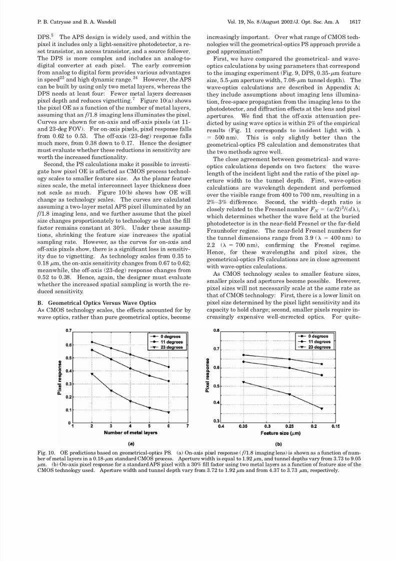
DPS.5 The APS design is widely used, and within thepixel it includes only a light-sensitive photodetector, a re-set transistor, an access transistor, and a source follower.The DPS is more complex and includes an analog-to-digital converter at each pixel. The early conversionfrom analog to digital form provides various advantagesin speed23 and high dynamic range.24 However, the APScan be built by using only two metal layers, whereas theDPS needs at least four: Fewer metal layers decreases
pixel depth and reduces vignetting.7 Figure 10(a) showsthe pixel OE as a function of the number of metal layers,assuming that an f /1.8 imaging lens illuminates the pixel.Curves are shown for on-axis and off-axis pixels (at 11-and 23-deg FOV). For on-axis pixels, pixel response fallsfrom 0.62 to 0.53. The off-axis (23-deg) response fallsmuch more, from 0.38 down to 0.17. Hence the designermust evaluate whether these reductions in sensitivity areworth the increased functionality.
Second, the PS calculations make it possible to investi-gate how pixel OE is affected as CMOS process technol-ogy scales to smaller feature size. As the planar featuresizes scale, the metal interconnect layer thickness doesnot scale as much. Figure 10(b) shows how OE willchange as technology scales. The curves are calculatedassuming a two-layer metal APS pixel illuminated by an
f /1.8 imaging lens, and we further assume that the pixelsize changes proportionately to technology so that the fillfactor remains constant at 30%. Under these assump-tions, shrinking the feature size increases the spatialsampling rate. However, as the curves for on-axis andoff-axis pixels show, there is a significant loss in sensitiv-ity due to vignetting. As technology scales from 0.35 to0.18 m, the on-axis sensitivity changes from 0.67 to 0.62;meanwhile, the off-axis (23-deg) response changes from0.52 to 0.38. Hence, again, the designer must evaluatewhether the increased spatial sampling is worth the re-duced sensitivity.
B. Geometrical Optics Versus Wave Optics As CMOS technology scales, the effects accounted for bywave optics, rather than pure geometrical optics, become
increasingly important. Over what range of CMOS tech-nologies will the geometrical-optics PS approach provide agood approximation?
First, we have compared the geometrical- and wave-optics calculations by using parameters that correspondto the imaging experiment (Fig. 9, DPS, 0.35- m featuresize, 5.5- m aperture width, 7.08- m tunnel depth). Thewave-optics calculations are described in Appendix A;they include assumptions about imaging lens illumina-tion, free-space propagation from the imaging lens to thephotodetector, and diffraction effects at the lens and pixelapertures. We find that the off-axis attenuation pre-dicted by using wave optics is within 2% of the empiricalresults (Fig. 11 corresponds to incident light with
ϭ 500 nm). This is only slightly better than thegeometrical-optics PS calculation and demonstrates thatthe two methods agree well.
The close agreement between geometrical- and wave-optics calculations depends on two factors: the wave-length of the incident light and the ratio of the pixel ap-erture width to the tunnel depth. First, wave-opticscalculations are wavelength dependent and performed
over the visible range from 400 to 700 nm, resulting in a2%–3% difference. Second, the width–depth ratio isclosely related to the Fresnel number F N ϭ (w /2)2 /(d),which determines whether the wave field at the buriedphotodetector is in the near-field Fresnel or the far-fieldFraunhofer regime. The near-field Fresnel numbers forthe tunnel dimensions range from 3.9 ( ϭ 400 nm) to2.2 ( ϭ 700 nm), confirming the Fresnel regime.Hence, for these wavelengths and pixel sizes, thegeometrical-optics PS calculations are in close agreementwith wave-optics calculations.
As CMOS technology scales to smaller feature sizes,smaller pixels and apertures become possible. However,pixel sizes will not necessarily scale at the same rate as
that of CMOS technology: First, there is a lower limit onpixel size determined by the pixel light sensitivity and itscapacity to hold charge; second, smaller pixels require in-creasingly expensive well-corrected optics. For quite-
Fig. 10. OE predictions based on geometrical-optics PS. (a) On-axis pixel response ( f /1.8 imaging lens) is shown as a function of num-ber of metal layers in a 0.18- m standard CMOS process. Aperture width is equal to 1.92 m, and tunnel depths vary from 3.73 to 9.05 m. (b) On-axis pixel response for a standard APS pixel with a 30% fill factor using two metal layers as a function of feature size of theCMOS technology used. Aperture width and tunnel depth vary from 3.72 to 1.92 m and from 4.37 to 3.73 m, respectively.
P. B. Catrysse and B. A. Wandell Vol. 19, No. 8 /August 2002 /J. Opt. Soc. Am. A 1617

7/30/2019 Optical Efficiency in Image Sensor pixels
http://slidepdf.com/reader/full/optical-efficiency-in-image-sensor-pixels 9/11
small pixel sizes, at the limit of what we anticipate as be-ing practical, deviations between the two calculations re-main in reasonable agreement. For example, consider atwo-layer metal APS pixel (0.18- m feature size, 1.92- maperture width, 3.73- m tunnel depth). In that case,the difference between geometrical- and wave-opticscalculations is less than 9%. We therefore expect thegeometrical-optics PS approach to remain a good approxi-mation to wave-optics calculations. Hence it will remaina valuable tool to predict the OE of CMOS image sensorpixels even as CMOS technology scales.
APPENDIX A1. Scattering-Matrix FormalismThe intuitive method of adding multiple reflected andtransmitted waves becomes quickly impractical even for afew dielectric layers. A more elegant approach that em-ploys 2 ϫ 2 matrices, referred to as the scattering-matrixapproach, will now be discussed. This method, pioneeredby Abeles,25,26 is based on the fact that the equations thatgovern the propagation of light are linear and that conti-nuity of the tangential components of the light fieldsacross an interface between two isotropic media can be re-garded as a 2 ϫ 2 linear matrix transformation. Thepresent development is due to Hayfield and White.21
Consider a stratified medium that consists of a stack of
m parallel layers sandwiched between two semi-infiniteambient (0) and substrate ( m ϩ 1) media. Let all mediabe linear homogeneous and isotropic, let the complex in-dex of refraction and the thickness of the jth layer be n j
and d j , respectively, and let n 0 and nmϩ1 represent thecomplex indices of refraction of the ambient and substratemedia. A monochromatic plane wave incident on the par-allel layers, originating from the ambient, generates a re-sultant transmitted plane wave in the substrate. We arenow interested in determining the amplitude of the re-sultant wave. The total field inside the jth layer, whichis excited by the incident plane wave, consists of two
plane waves: a forward-traveling and a backward-traveling plane wave with complex amplitudes Eϩ and
EϪ, respectively.The total field in a plane z, parallel to the boundary,
can be described by a 2 ϫ 1 column vector:
E z ϭ Eϩ z
EϪ z . (A1)
If we consider the fields at two different planes zЈ
and zЉ,by virtue of linearity, E( zЈ) and E( zЉ) are related by a
2 ϫ 2 matrix transformation:
Eϩ z Ј
EϪ z Ј ϭ S11 S12
S21 S22 Eϩ z Љ
EϪ z Љ . (A2)
The 2 ϫ 2 matrix defined by the planes immediately ad- jacent to the 01 and m(m ϩ 1) interfaces is called thescattering matrix S. The scattering matrix representsthe overall reflection and transmission properties of thestratified structure and can be expressed as a product of interface and layer matrices I and L that describe the en-tire stratified structure:
S ϭ I01L1¯
I jϪ1 jL j¯
LmIm mϩ1 . (A3)
The matrix I of an interface between two media relatesthe fields on both its sides by using Fresnel’s reflectionand transmission coefficients for the interface:
I jϪ1 j ϭ 1/ t jϪ1 j 1 r jϪ1 j
r jϪ1 j 1 . (A4)
The interface Fresnel transmission and reflection coeffi-cients t ( jϪ1) j and r( jϪ1) j are evaluated by using the com-plex indices of refraction of the two media that define theinterface and the local angle of incidence by repeated ap-plication of Snell’s law:
n0 sin 0 ϭ¯ϭ n j sin j ϭ ¯ ϭ nmϩ1 sin mϩ1 . (A5)
The formulas to compute the Fresnel coefficients can befound in many optics textbooks27; the complex indices of refraction are dependent on the material used in theCMOS process. We now turn our attention to the effectof propagation through a homogeneous layer of index of refraction n j and thickness d j . The layer matrix L canbe written as
L j ϭ exp j j 0
0 exp Ϫ j j , (A6)
where the layer phase thickness  j is given by
 j ϭ2
d j n j cos j . (A7)
The overall reflection ( R) and transmission (T ) coefficientsof the stratified structure are
R ϭ
S21
S11
, (A8)
T ϭ1
S 21
. (A9)
Fig. 11. Comparison of geometrical-optics PS and wave-opticsapproaches to calculating pixel OE as a function of angle of inci-dence of the chief ray of an f /1.8 imaging lens with a full FOV of 23 deg. The computed pixel OE includes both geometric andtransmission efficiency. When these theoretical curves are plot-ted with the data in Fig. 9, both the theory and the data are nor-malized to the on-axis pixel OE, effectively removing the trans-mission loss.
1618 J. Opt. Soc. Am. A /Vol. 19, No. 8 /August 2002 P. B. Catrysse and B. A. Wandell

7/30/2019 Optical Efficiency in Image Sensor pixels
http://slidepdf.com/reader/full/optical-efficiency-in-image-sensor-pixels 10/11
We use these formulas to calculate the overall transmis-sion efficiency of the dielectric tunnel from the pixel aper-ture at the surface to the photodetector on the pixel floorby treating the tunnel as a dielectric stack of N layers.In the case of a DPS in 0.35- m CMOS technology, thereare six layers with refractive indices varying from 1.48 to3.44 and thicknesses ranging from 1 to 1.67 m. We per-form the calculation for a wide range of angles of inci-dence and do this for every wavelength in the visible
wavelength band between 400 and 700 nm. We then av-erage the angle dependency over all wavelengths to pro-duce the transmission efficiency plot in Fig. 6. We notethat most of the transmission losses occur at the initialair–Si3N4 interface and the final SiO2–Si interface withminor losses at the intermediate interfaces.
2. Wave-Optics CalculationWe describe in this paper an intuitive geometrical-opticsPS model to calculate the OE of image sensor pixels.This description can be extended to include wave-opticsphenomena, such as diffraction, interference, coherence,and polarization. However, this requires a six-dimensional coordinate frame ( x , y, p, q, t, ) and leadsto a computationally more intensive PS representationbased on the Wigner transform.14,15 Instead, we optedfor a comparison of the geometrical-optics PS prediction of the OE with a straightforward wave-optics prediction.This allows us to evaluate the effect of diffraction at thelens rim and at the finite pixel aperture on the OE. Weshowed that the two predictions are very similar. In thissection, we describe the steps used in calculating the OEof a pixel at the image plane of a lens within the wave-optics framework.
Consider an imaging system consisting of an imaging lens with a finite aperture diameter, illuminated by a set
of plane waves. The plane waves are imaged onto a sen-sor plane containing a pixel of finite aperture size and aburied photodetector. Assume that (1) we model incoher-ent imaging, (2) we perform the calculations for the vis-ible range of wavelengths from 400 to 700 nm, (3) we useboth the paraxial Fresnel propagation kernel and a non-paraxial wide-angle kernel when performing free-spacepropagation from object plane to lens plane and from lensplane to imaging plane, and (4) we include the effect of evanescent waves.
The optical wave field defined at the object plane,U o( x, y, 0), is converted into its angular spectrum:
A o
␣
,
; 0 ϭ
Ϫ͵ϱ
ϱ
Ϫ͵ϱ
ϱ
U o x , y, 0
ϫ exp Ϫ j2 ␣
x ϩ

y d xd y.
(A10)
It is propagated over the free-space object distance z o byusing paraxial propagation kernels, leading to
A o
␣
,
; z o ϭ A o
␣
,
; 0 exp j
2
z o
ϫ exp Ϫ j z o ␣
2
ϩ 
2
,
(A11)
or nonparaxial propagation kernels, leading to
A o
␣
,
; z o ϭ A o
␣
,
; 0
ϫ exp j2
1 Ϫ ␣ 2 Ϫ  2 1/2 z o .
(A12)
At the plane of the imaging lens, we convert the incidentspectrum back into a wave field, given by
U o x , y , z o ϭ
Ϫ͵ϱ
ϱ
Ϫ͵ϱ
ϱ
A o
␣
,
; z o
ϫ exp j2 ␣
x ϩ

y d
␣
d
,
(A13)
to allow for interaction with the phase and amplitude dis-tribution of the lens, i.e., a quadratic phase factor and afinite aperture defined by the pupil function P( x, y),yielding
U l x, y , z o ϭ P x, y exp jk
2 f x 2
ϩ y2 U o x, y, z o .
(A14)
The transmitted field U l
( x, y, zo
) is then again convertedinto its angular spectrum A l(␣ / ,  / ; z o) as shownabove and propagated over the free-space imaging dis-tance z i to yield A i(␣ / , ␣ / ; z o ϩ z i). At the imaging plane, the field U i( x, y , z o ϩ z i) interacts with the aper-ture of the pixel t p( x, y), and the resulting fieldU p( x, y , z o ϩ z i) ϭ t p( x, y)U l( x, y, z o ϩ z i) is oncemore converted and propagated over the pixel depth d be-fore reaching the photodetector where it is collectedU p( x, y , z o ϩ z i ϩ d). We compare the energy con-tained within the field incident on the pixel area,U p( x, y , z o ϩ z i), with the energy contained within thefield incident on the photodetector area, U p( x, y, z o ϩ z i
ϩ d), by integration of the respective fields over the re-spective areas of the pixel aperture and the photodetector.The OE is here defined as the ratio of these integrals.
ACKNOWLEDGMENTS
This work is supported by the Programmable DigitalCamera project, by Agilent Technologies, and by PhilipsSemiconductors. P. B. Catrysse is ‘‘Aspirant’’ with theFund for Scientific Research–Flanders (Belgium). Wethank A. El Gamal, R. Byer, H. Thienpont, I. Veretenni-coff, B. Fowler, R. Piestun, J. DiCarlo, Y. Takashima, andF. Xiao for valuable discussions and helpful comments.
P. B. Catrysse and B. A. Wandell Vol. 19, No. 8 /August 2002 /J. Opt. Soc. Am. A 1619
7/30/2019 Optical Efficiency in Image Sensor pixels
http://slidepdf.com/reader/full/optical-efficiency-in-image-sensor-pixels 11/11
Address correspondence to Peter B. Catrysse (c/o Wan-dell Lab), Jordan Hall, Building 420, Room 490, StanfordUniversity, Stanford, California 94305-2130. Phone,650-725-1255; fax, 650-723-0993; e-mail, peter
@kaos.stanford.edu.
REFERENCES1. J. R. Janesick, K. Evans, and T. Elliot, ‘‘Charge-coupled-
device response to electron beam energies of less than 1 keV up to 20 keV,’’ Opt. Eng. 26, 686–691 (1987).
2. B. Fowler, A. El Gamal, D. Yang, and H. Tian, ‘‘A method forestimating quantum efficiency for CMOS image sensors,’’ in Solid State Sensor Arrays: Development and Applications II , M. M. Blouke, ed., Proc. SPIE 3301, 178–185 (1998).
3. D. Yang, H. Tian, B. Fowler, X. Liu, and A. El Gamal, ‘‘Char-acterization of CMOS image sensors with Nyquist ratepixel level ADC,’’ in Sensors, Cameras, and Applications for Digital Photography, N. Sampat and T. Yeh, eds., Proc.SPIE 3650, 52–62 (1999).
4. J. Giest and H. Baltes, ‘‘High accuracy modeling of photodi-ode quantum efficiency,’’ Appl. Opt. 28, 3929–3938 (1989).
5. D. Yang, A. El Gamal, B. Fowler, and H. Tian, ‘‘A 640ϫ 512 CMOS image sensor with ultrawide dynamic rangefloating-point pixel-level ADC,’’ IEEE J. Solid-State Circuits34, 1821–1834 (1999).
6. J. A. Penkethman, ‘‘Calibrations and idiosyncrasies of micro-lensed CCD cameras,’’ in Current Developments inOptical Design and Optical Engineering VIII , R. E. Fischerand W. J. Smith, eds., Proc. SPIE 3779, 241–249 (1999).
7. P. Catrysse, X. Liu, and A. El Gamal, ‘‘QE reduction due topixel vignetting in CMOS image sensors,’’ in Sensors andCamera Systems for Scientific, Industrial, and Digital Pho-tography Applications, M. M. Blouke, N. Sampat, G. M. Wil-liams, Jr., and T. Yeh, eds., Proc. SPIE 3965, 420–430(2000).
8. Luminous, Silvaco International, Santa Clara, Calif., 1995.9. Medici, Avanti Corporation, Fremont, Calif., 1998.
10. M. Hideki, ‘‘Simulation for 3-D optical and electrical analy-sis of CCD,’’ IEEE Trans. Electron Devices 44, 1604–1610(1997).
11. R. J. Pegis, ‘‘The modern development of Hamiltonian op-tics,’’ in Progress in Optics I , E. Wolf, ed. (North-Holland, Amsterdam, 1961), pp. 1–29.
12. R. Winston, ‘‘Light collection within the framework of geo-metrical optics,’’ J. Opt. Soc. Am. 60, 245–247 (1970).
13. J. W. Goodman, Introduction to Fourier Optics, 2nd ed.(McGraw-Hill, San Francisco, Calif., 1996), p. 404.
14. M. J. Bastiaans, ‘‘Wigner distribution function and its ap-plication to first-order optics,’’ J. Opt. Soc. Am. 69, 1710–1716 (1979).
15. D. Dragoman, ‘‘The Wigner distribution function in opticsand optoelectronics,’’ in Progress in Optics XXXVII , E. Wolf,ed. (Elsevier Science, Amsterdam, 1997), pp. 1–56.
16. A. Walther, ‘‘Gabor’s theorem and energy transfer throughlenses,’’ J. Opt. Soc. Am. 57, 639–644 (1967).
17. R. N. Bracewell, The Fourier Transform and Its Applica-tions, 2nd ed. (McGraw-Hill, New York, 1986), p. 52.
18. W. H. Steel, ‘‘Luminosity, throughput, or etendue,’’ Appl.Opt. 13, 704–705 (1974).
19. A. A. Lohmann, R. G. Dorsch, D. Mendlovic, Z. Zalevsky,and C. Ferreira, ‘‘Space–bandwidth product of optical sig-nals and systems,’’ J. Opt. Soc. Am. A 13, 470–473 (1996).
20. M. J. Bastiaans, ‘‘The Wigner distribution function appliedto optical signals and systems,’’ Opt. Commun. 25, 26–30(1978).
21. P. C. S. Hayfield and G. W. T. White, ‘‘An assessment of thesuitability of the Drude–Tronstad polarized light methodfor the study of film growth on polycrystalline metals,’’ in Ellipsometry in the Measurement of Surfaces and Thin Films, N. M. Bashara, A. B. Buckman, and A. C. Hall, eds.(National Bureau of Standards, Washington, D.C., 1964), Vol. 256, pp. 157–200.
22. E. R. Fossum, ‘‘Active pixel sensors: are CCD’s dinosaurs?’’in Charge-Coupled Devices and Solid State Optical Sensors
III , M. M. Blouke, ed., Proc. SPIE 1900, 2–
14 (1993).23. S. Kleinfelder, S. Lim, X. Liu, and A. El Gamal, ‘‘A 10kframes/s 0.18 m CMOS digital pixel sensor with pixel-level memory,’’ in 2001 International Solid-State CircuitsConference—Digest of Technical Papers (IEEE Press, Pis-cataway, N.J., 2001), pp. 88–89.
24. B. Wandell, P. Catrysse, J. DiCarlo, D. Yang, and A. El Ga-mal, ‘‘Multiple capture single image architecture with aCMOS sensor,’’ in Proceedings of the International Sympo-sium on Multispectral Imaging and Color Reproduction for Digital Archives (Society of Multispectral Imaging of Japan,Chiba, Japan, 1999), pp. 11–17.
25. F. Abeles, ‘‘Recherches sur la propagation des ondes electro-magnetiques sinusoidales dans les milieux stratifies: ap-plication aux couches minces,’’ Ann. Phys. (Paris) 5, 596–640 (1950).
26. F. Abeles, ‘‘Recherches sur la propagation des ondes electro-
magnetiques sinusoidales dans les milieux stratifies: ap-plication aux couches minces,’’ Ann. Phys. (Paris) 5, 706–782 (1950).
27. M. Born and E. Wolf, Principles of Optics, 6th (corrected)ed. (Pergamon, Oxford, UK, 1980), pp. 38–41.
1620 J. Opt. Soc. Am. A /Vol. 19, No. 8 /August 2002 P. B. Catrysse and B. A. Wandell