operational amplifiers
TRANSCRIPT

1
Slides taken from:
A.R. Hambley, Electronics, © Prentice Hall, 2/e, 2000
A. Sedra and K.C. Smith, Microelectronic Circuits, © Oxford University Press, 4/e, 1999
Operational Amplifiers

2Figure 2.1 Circuit symbol for the op amp.
Operational Amplifier Symbol

3Figure 2.3 Op-amp symbol showing power supplies.
Operational Amplifier Symbol

4
Internal Structure of Op Amps
+
-
vid
vo
+
-
TranscoductanceDifferentialAmplifier
High GainVoltage
Amplifier
UnityGain
Buffer
C
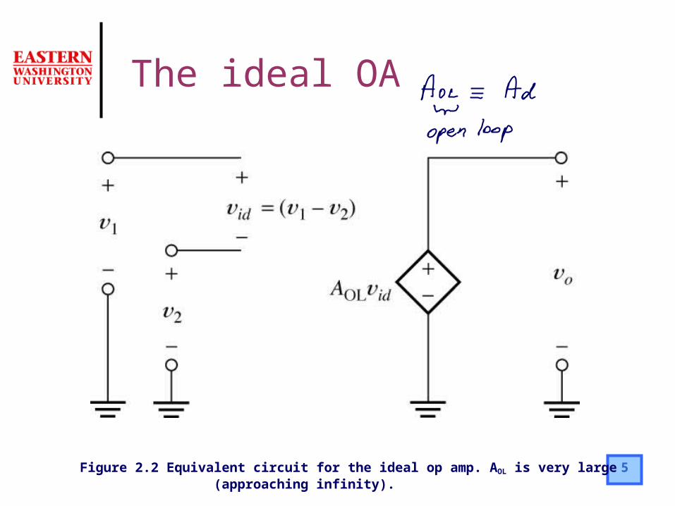
5Figure 2.2 Equivalent circuit for the ideal op amp. AOL is very large (approaching infinity).
The ideal OA

6
The ideal OA
Infinite input impedance Infinite open-loop gain for the differential input Zero gain for the common mode signal Zero output impedance Infinite Bandwidth
7
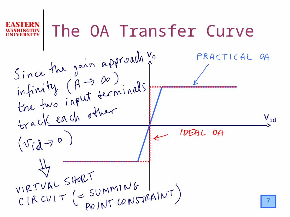
The OA Transfer CurvevO
vid

8
Feedback
Negative FeedbackPart of the output signal is returned to the input
in opposition to the source signal
Positive FeedbackThe signal returned from the output to the input
aids the original source signal

9
Figure 2.5 Inverting amplifier.
The Inverting Amplifier

10Fig. 2.5 Analysis of the inverting configuration
Analysis of the Inverting Amplifier
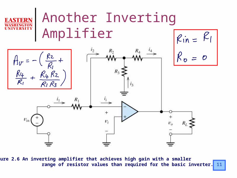
11Figure 2.6 An inverting amplifier that achieves high gain with a smaller range of resistor values than required for the basic inverter.
Another Inverting Amplifier
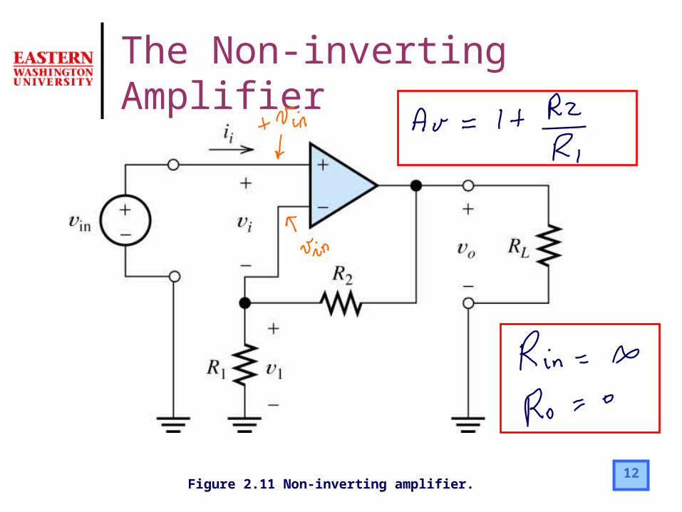
12Figure 2.11 Non-inverting amplifier.
The Non-inverting Amplifier

13Figure 2.12 Voltage Follower.
The Voltage Follower

14
Figure 2.14 Difference amplifier.
Difference Amplifier (1)

15
Fig. 2.22 Application of superposition to the analysis of the difference amplifier
Difference Amplifier (2)
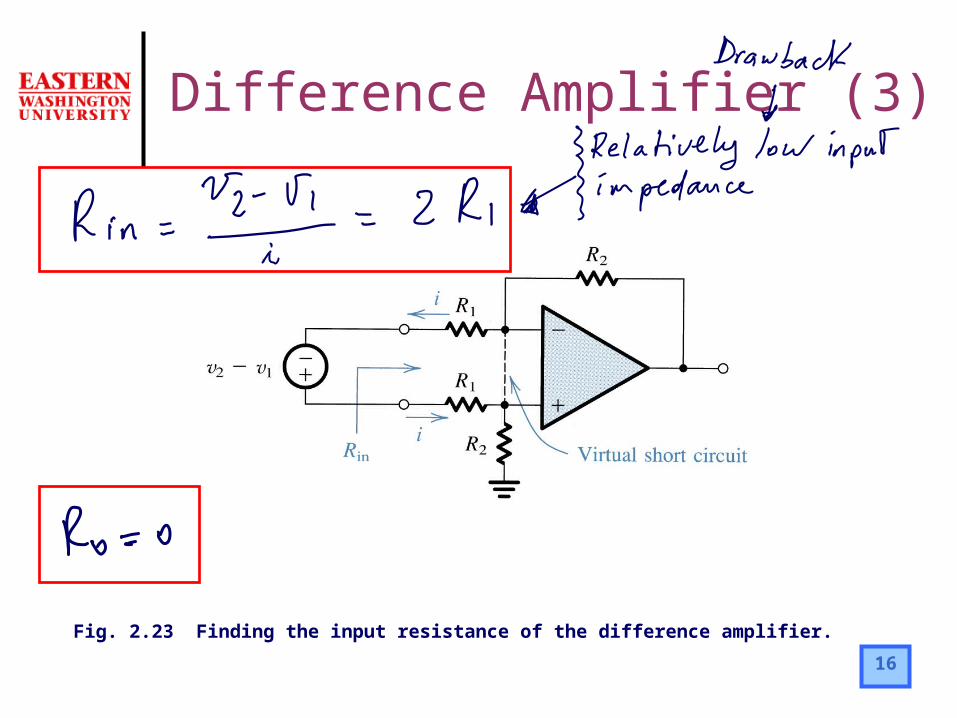
16
Fig. 2.23 Finding the input resistance of the difference amplifier.
Difference Amplifier (3)

17
Figure 2.7 Summing amplifier.
Summing Amplifier
18
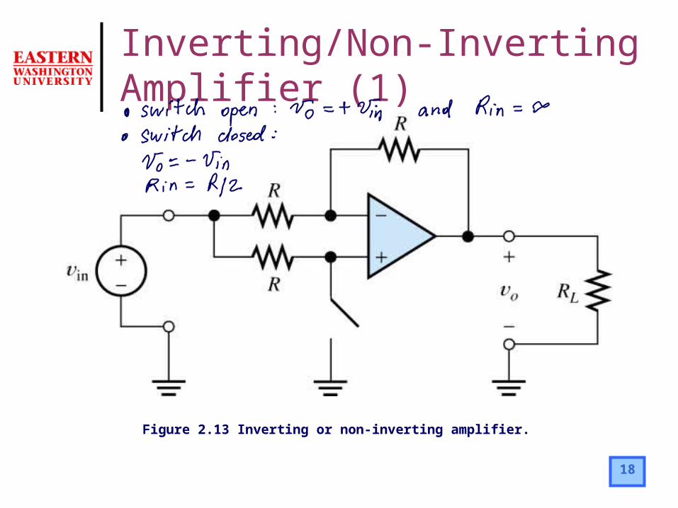
Figure 2.13 Inverting or non-inverting amplifier.
Inverting/Non-Inverting Amplifier (1)
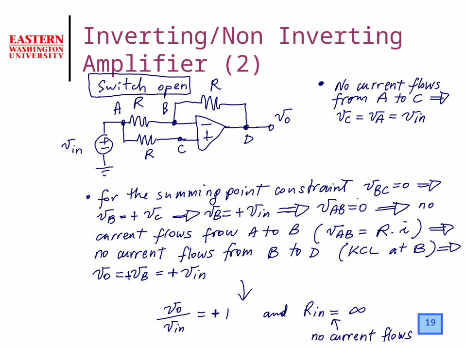
19
Inverting/Non Inverting Amplifier (2)

20
Inverting/Non inverting Amplifier (3)
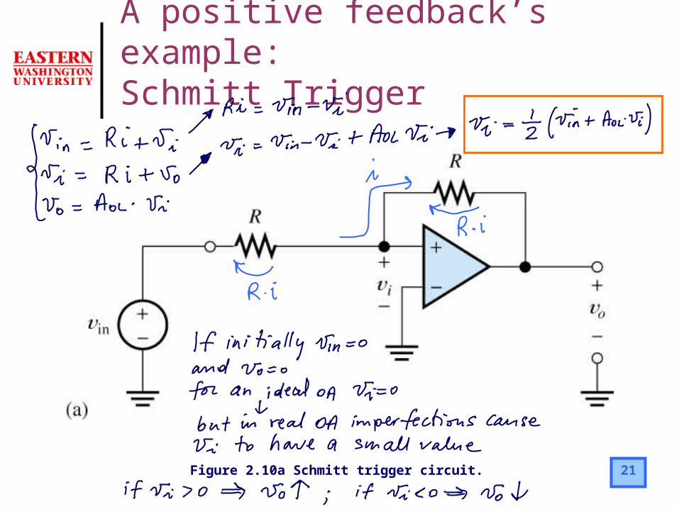
21Figure 2.10a Schmitt trigger circuit.
A positive feedback’s example: Schmitt Trigger

22Figure 2.10b Schmitt trigger circuit and waveforms.
A positive feedback’s example: Schmitt Trigger
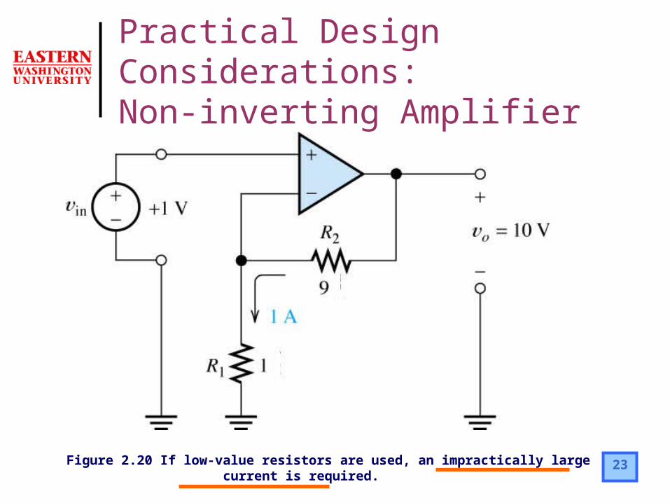
23Figure 2.20 If low-value resistors are used, an impractically large current is required.
Practical Design Considerations:Non-inverting Amplifier
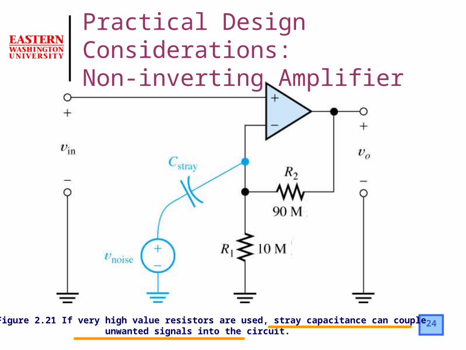
24Figure 2.21 If very high value resistors are used, stray capacitance can couple unwanted signals into the circuit.
Practical Design Considerations:Non-inverting Amplifier

25
Figure 2.22 To attain large input resistance with moderate resistances for an inverting amplifier we cascade a voltage follower with an inverter.
Practical Design Considerations:Inverting Amplifier
26
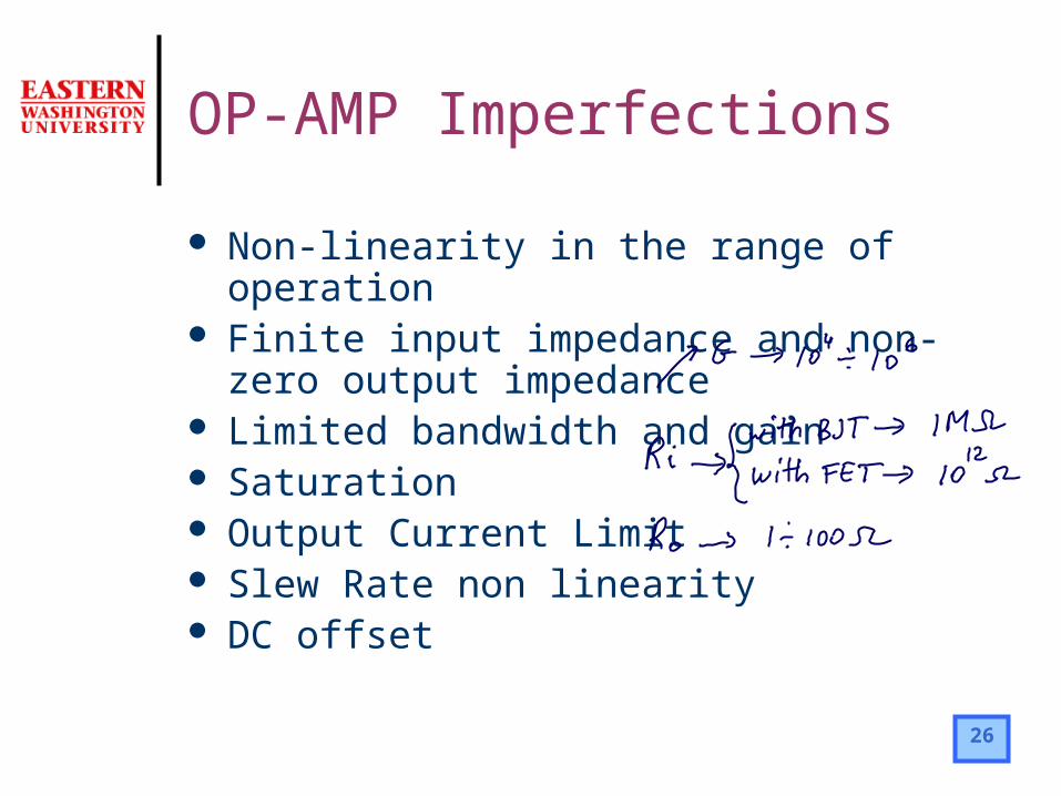
OP-AMP Imperfections
Non-linearity in the range of operation Finite input impedance and non-zero output
impedance Limited bandwidth and gain Saturation Output Current Limit Slew Rate non linearity DC offset

27Figure 2.25 Bode plot of open-loop gain for a typical op amp.
Gain and Bandwidth Limitations

28Figure 2.26 Non-inverting amplifier.
Effect of the gain and bandwidth limitations.
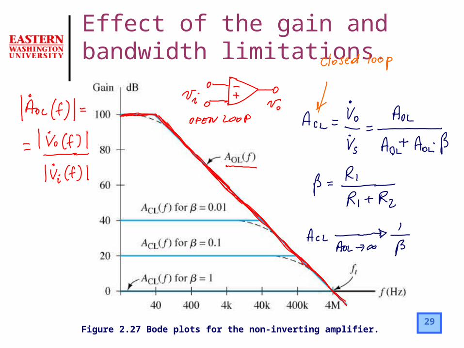
29Figure 2.27 Bode plots for the non-inverting amplifier.
Effect of the gain and bandwidth limitations.

30Figure 2.28 For a real op amp, clipping occurs if the output voltage reaches certain limits.
Saturation

31
Output Current Limit
The current that an op amp can supply to a load is limited (typically +/-25 mA)
If a small-value load draw a current outside the limit, the output waveform becomes clipped

32Figure 2.30 Output for R1=1Kohm R2= 3Kohm RL = 10kohm and Vs max = 5V.
Max Output Voltage Swing

33
Slew Rate Limitation
The output voltage of an op amp cannot change in magnitude at a rate exceeding the slew rate limit

34Figure 2.31 Output for RL = 10kohm and vs(t) = 2.5 sin (105 t).
Effect of Slew Rate Limitation

35
Effect of Slew Rate Limitation
Fig. 2.29 (a) Unity-gain follower. (b) Input step waveform. (c) Linearly rising output waveform obtained when the amplifier is slew-rate limited.

36
Effect of Slew Rate Limitation
Full-power bandwidth fFPB: range of frequencies for which the op amp can
produce an undistorted sinusoidal output with peak amplitude equal to the guaranteed maximum output voltage.

37
DC Imperfections
Input Bias Current
Input Offset Current
Input Offset Voltage

38Figure 2.33 Current sources and a voltage source model the dc imperfections of an op amp.
Modeling DC Imperfections

39
Modeling DC Imperfections
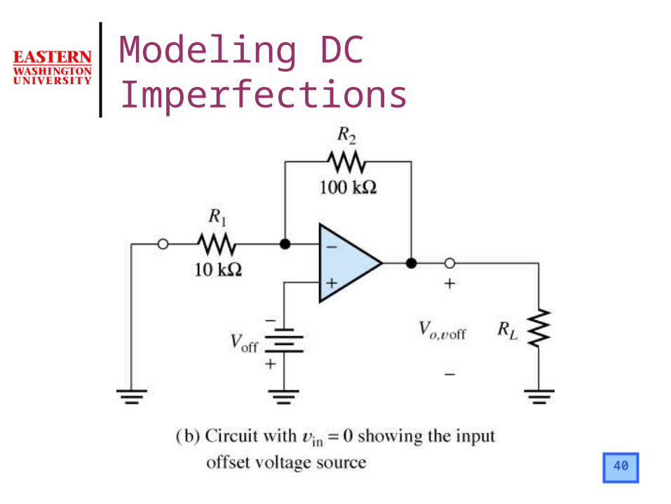
40
Modeling DC Imperfections
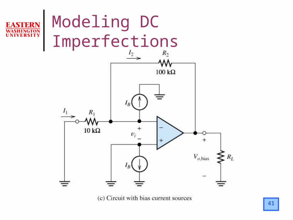
41
Modeling DC Imperfections
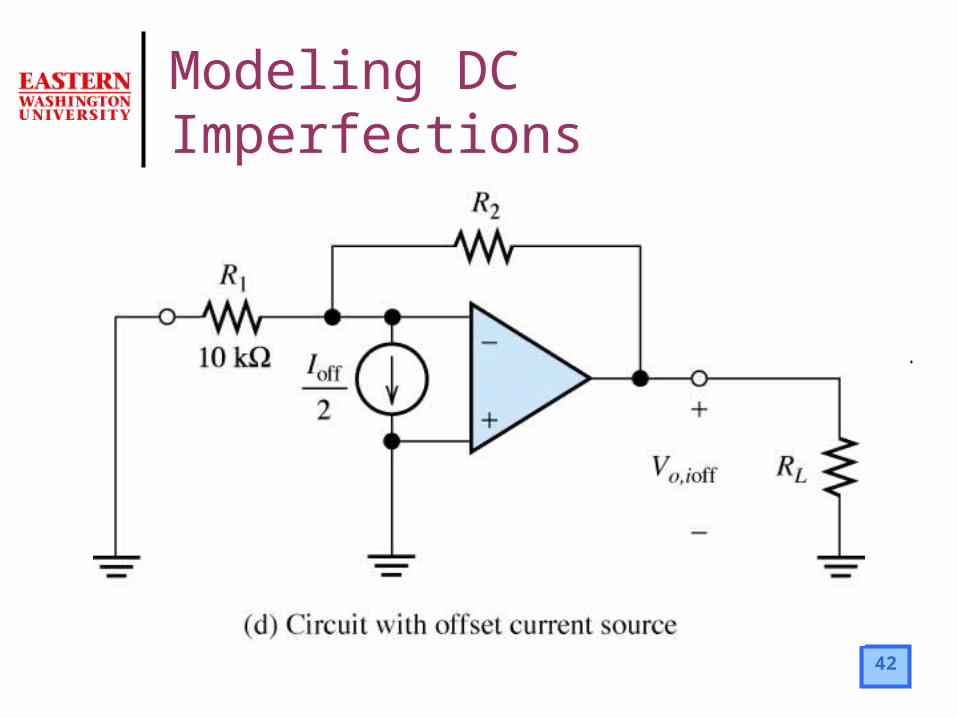
42
Modeling DC Imperfections
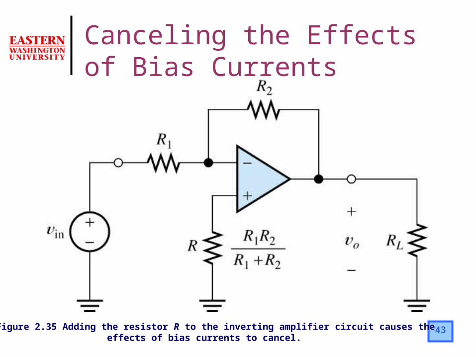
43Figure 2.35 Adding the resistor R to the inverting amplifier circuit causes the effects of bias currents to cancel.
Canceling the Effects of Bias Currents

44Figure 2.36 Non-inverting amplifier, including resistor R to balance the effects of the bias currents.
Canceling the Effects of Bias Currents

45
Figure 2.46 Unity-gain amplifiers.
Common OA Circuits: unity gain amplifiers

46Figure 2.47 Inverting amplifier.
Common OA Circuits: Inverting Amplifier
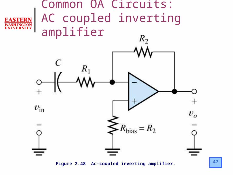
47Figure 2.48 Ac-coupled inverting amplifier.
Common OA Circuits: AC coupled inverting amplifier

48Figure 2.49 Summing amplifier.
Common OA Circuits: Summing Amplifier

49Figure 2.50 Non-inverting amplifier. This circuit approximates an ideal voltage amplifier.
Common OA Circuits: Non-Inverting Ampl.
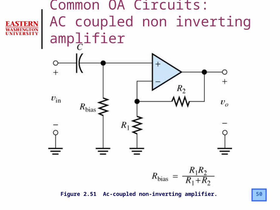
50Figure 2.51 Ac-coupled non-inverting amplifier.
Common OA Circuits: AC coupled non inverting amplifier

51Figure 2.52 Ac-coupled voltage follower with bootstrapped bias resistors.
AC coupled follower (1)
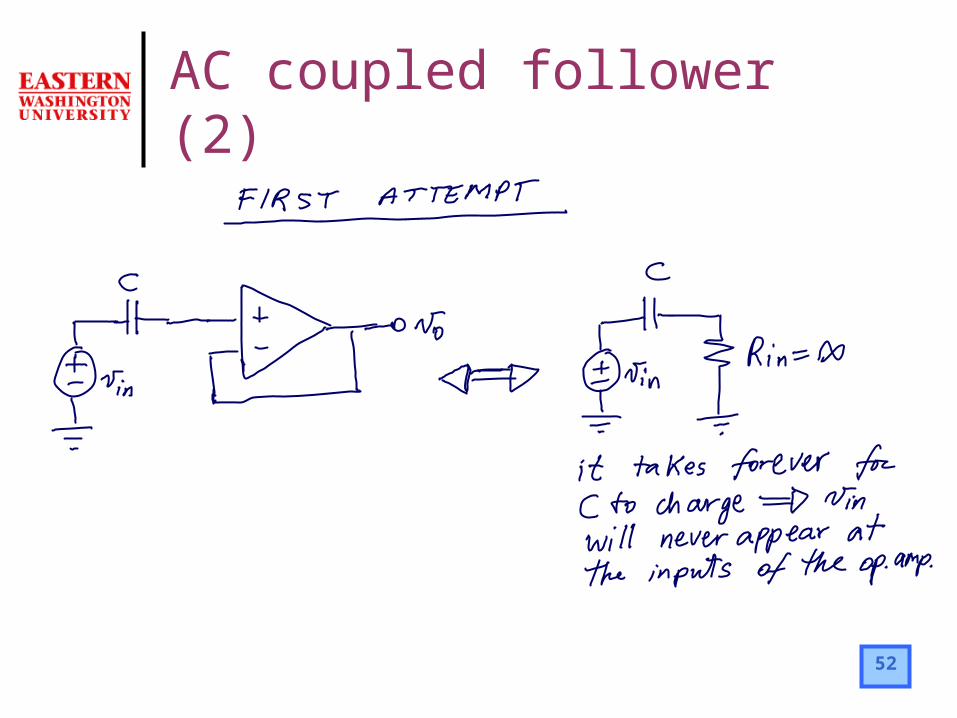
52
AC coupled follower (2)

53
AC coupled follower (3)

54
AC coupled follower (4)

55
AC coupled follower (5)

56Figure 2.53 Difference amplifier.
Common OA Circuits: Difference Amplifier

57Figure 2.54 Instrumentation-quality differential amplifier.
Common OA Circuits: Instrumentation Difference Amplifier

58Figure 2.55 Voltage-to-current converter (transconductance amplifier).
Common OA Circuits: Voltage/Current Converter

59Figure 2.56 Voltage-to-current converter with grounded load.
Common OA Circuits: Voltage/Current Converter (Inverting)

60Figure 2.56 Voltage-to-current converter with grounded load.
Voltage/Current Converter (Non Inverting)(step 1)
61
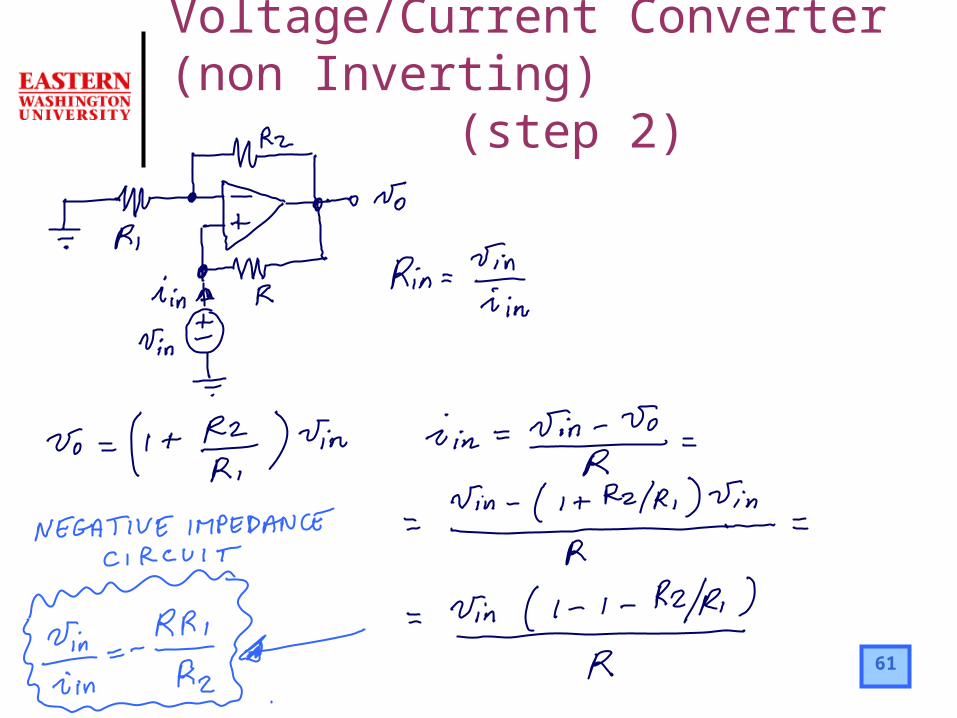
Voltage/Current Converter (non Inverting)(step 2)

62
Voltage/Current converter (step 3)

63Figure 2.57 Current-to-voltage converter (transresistance amplifier).
Common OA Circuits: Current/Voltage Converter
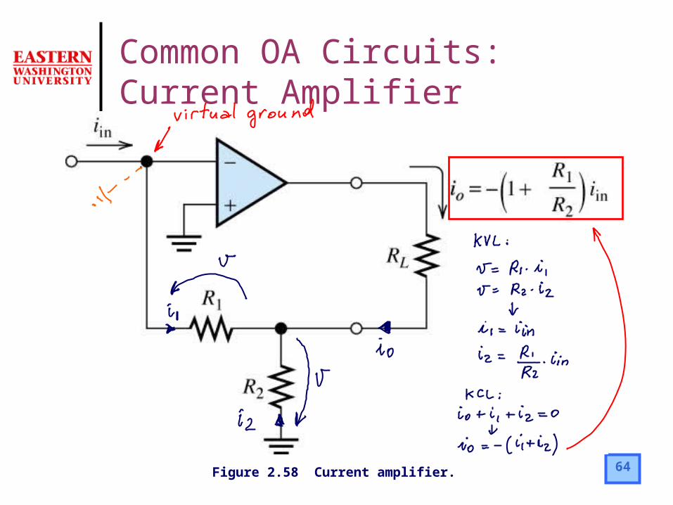
64Figure 2.58 Current amplifier.
Common OA Circuits: Current Amplifier

65Figure 2.59 Variable-gain amplifier.
Common OA Circuits: Variable Gain Ampl.

66
Common OA Circuits: Filters
-
+
+
-+
-
Z2
Z1

67Figure 2.60 Integrator Filter.
Common OA Circuits: Integrator

68Figure 2.63 Differentiator Filter.
Common OA Circuits: Derivator
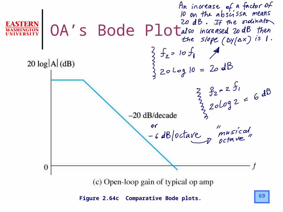
69Figure 2.64c Comparative Bode plots.
OA’s Bode Plot

70Figure 2.64a Comparative Bode plots.
Integrator’s Bode Plot
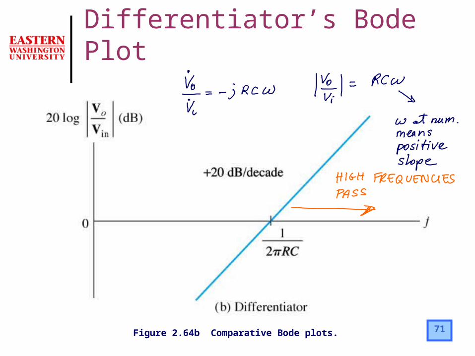
71Figure 2.64b Comparative Bode plots.
Differentiator’s Bode Plot