opa211-ht - texas instruments · input voltage noise density vs frequency) Ö hz 0.1 100 1...
TRANSCRIPT
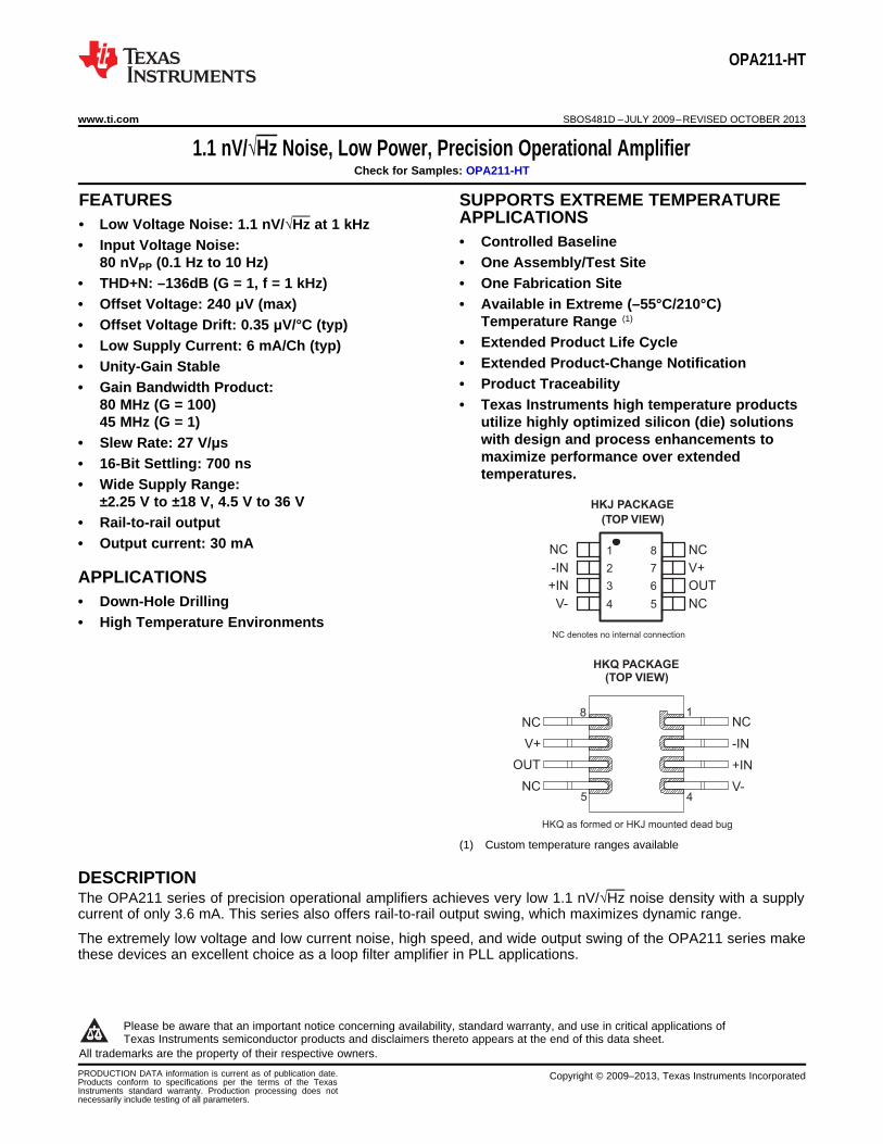
HKQ PACKAGE(TOP VIEW)
8
5 4
1
HKQ as formed or HKJ mounted dead bug
NC
-IN
+IN
V-
NC
V+
OUT
NC
1
2
3
4
8
7
6
5
NC
-IN
+IN
V-
NC
V+
OUT
NC
HKJ PACKAGE
(TOP VIEW)
NC denotes no internal connection
OPA211-HT
www.ti.com SBOS481D –JULY 2009–REVISED OCTOBER 2013
1.1 nV/√Hz Noise, Low Power, Precision Operational AmplifierCheck for Samples: OPA211-HT
1FEATURES SUPPORTS EXTREME TEMPERATUREAPPLICATIONS
2• Low Voltage Noise: 1.1 nV/√Hz at 1 kHz• Controlled Baseline• Input Voltage Noise:
80 nVPP (0.1 Hz to 10 Hz) • One Assembly/Test Site• THD+N: –136dB (G = 1, f = 1 kHz) • One Fabrication Site• Offset Voltage: 240 μV (max) • Available in Extreme (–55°C/210°C)
Temperature Range (1)• Offset Voltage Drift: 0.35 μV/°C (typ)• Extended Product Life Cycle• Low Supply Current: 6 mA/Ch (typ)• Extended Product-Change Notification• Unity-Gain Stable• Product Traceability• Gain Bandwidth Product:
80 MHz (G = 100) • Texas Instruments high temperature products45 MHz (G = 1) utilize highly optimized silicon (die) solutions
with design and process enhancements to• Slew Rate: 27 V/μsmaximize performance over extended• 16-Bit Settling: 700 nstemperatures.
• Wide Supply Range:±2.25 V to ±18 V, 4.5 V to 36 V
• Rail-to-rail output• Output current: 30 mA
APPLICATIONS• Down-Hole Drilling• High Temperature Environments
(1) Custom temperature ranges available
DESCRIPTIONThe OPA211 series of precision operational amplifiers achieves very low 1.1 nV/√Hz noise density with a supplycurrent of only 3.6 mA. This series also offers rail-to-rail output swing, which maximizes dynamic range.
The extremely low voltage and low current noise, high speed, and wide output swing of the OPA211 series makethese devices an excellent choice as a loop filter amplifier in PLL applications.
1
Please be aware that an important notice concerning availability, standard warranty, and use in critical applications ofTexas Instruments semiconductor products and disclaimers thereto appears at the end of this data sheet.
2All trademarks are the property of their respective owners.PRODUCTION DATA information is current as of publication date. Copyright © 2009–2013, Texas Instruments IncorporatedProducts conform to specifications per the terms of the TexasInstruments standard warranty. Production processing does notnecessarily include testing of all parameters.

INPUT VOLTAGE NOISE DENSITY vs FREQUENCY
Voltage N
ois
e D
ensity (
nV
/)
ÖH
z
0.1
100
1
Frequency (Hz)
100k101
10
100 1k 10k
OPA211-HT
SBOS481D –JULY 2009–REVISED OCTOBER 2013 www.ti.com
In precision data acquisition applications, the OPA211 series of op amps provides 700-ns settling time to 16-bitaccuracy throughout 10-V output swings. This ac performance, combined with only 240-μV of offset and 0.35-μV/°C of drift over temperature, makes the OPA211 ideal for driving high-precision 16-bit analog-to-digitalconverters (ADCs) or buffering the output of high-resolution digital-to-analog converters (DACs).
The OPA211 series is specified over a wide dual-power supply range of ±2.25 V to ±18 V, or for single-supplyoperation from 4.5 V to 36 V.
This series of op amps is specified from TA = –55°C to 210°C.
Table 1. ORDERING INFORMATION (1)
TA PACKAGE ORDERABLE PART NUMBER TOP-SIDE MARKINGHKJ OPA211SHKJ OPA211SHKJ
–55°C to 210°C HKQ OPA211SHKQ OPA211SHKQKGD OPA211SKGD1 NA
(1) For the most current package and ordering information, see the Package Option Addendum at the end of this document, or see the TIWeb site at www.ti.com.
This integrated circuit can be damaged by ESD. Texas Instruments recommends that all integrated circuits be handled withappropriate precautions. Failure to observe proper handling and installation procedures can cause damage.
ESD damage can range from subtle performance degradation to complete device failure. Precision integrated circuits may be moresusceptible to damage because very small parametric changes could cause the device not to meet its published specifications.
2 Submit Documentation Feedback Copyright © 2009–2013, Texas Instruments Incorporated
Product Folder Links: OPA211-HT
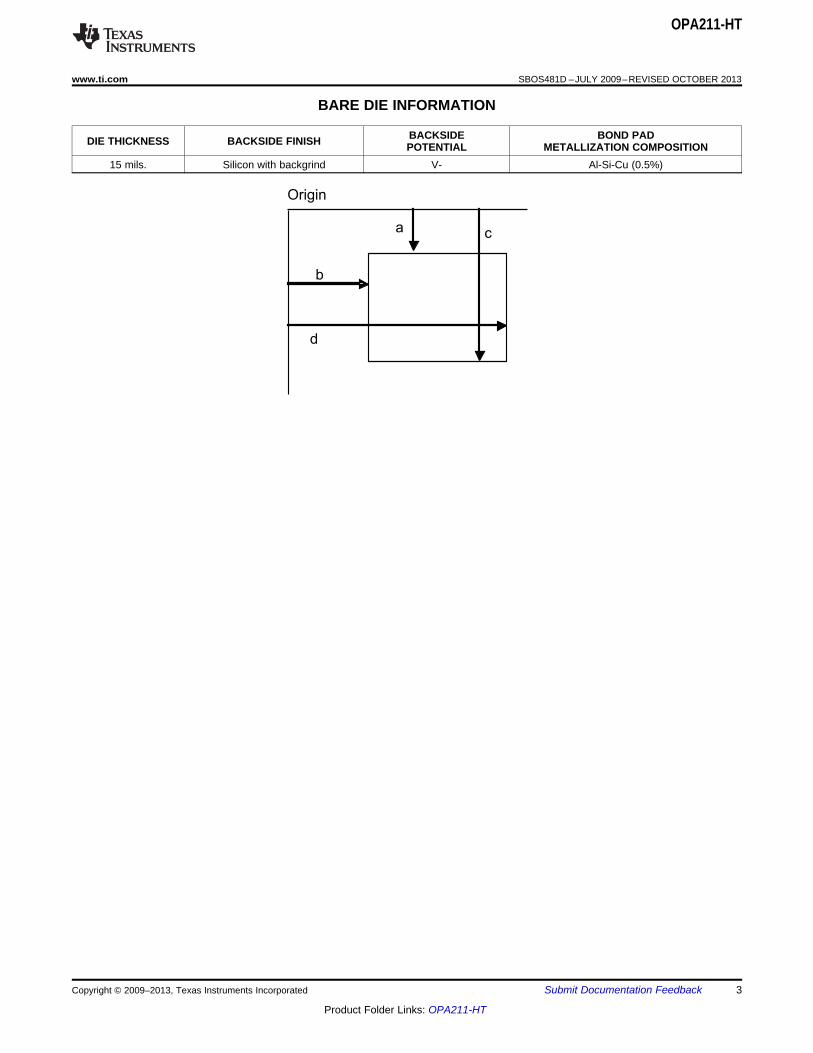
a
b
c
d
Origin
OPA211-HT
www.ti.com SBOS481D –JULY 2009–REVISED OCTOBER 2013
BARE DIE INFORMATION
BACKSIDE BOND PADDIE THICKNESS BACKSIDE FINISH POTENTIAL METALLIZATION COMPOSITION15 mils. Silicon with backgrind V- Al-Si-Cu (0.5%)
Copyright © 2009–2013, Texas Instruments Incorporated Submit Documentation Feedback 3
Product Folder Links: OPA211-HT

OPA211-HT
SBOS481D –JULY 2009–REVISED OCTOBER 2013 www.ti.com
Table 2. BOND PAD COORDINATESDESCRIPTION PAD NUMBER a b c d
-IN 1 34.4000 792.000 109.400 867.000+IN 2 34.4000 33.000 109.400 108.000NC 3 461.850 33.000 536.850 108.000V- 4 692.650 54.600 767.650 129.600
OUT 5 920.400 33.000 995.400 108.000V+ 6 920.400 720.150 995.400 795.150NC 7 388.050 792.000 463.050 867.000
4 Submit Documentation Feedback Copyright © 2009–2013, Texas Instruments Incorporated
Product Folder Links: OPA211-HT

OPA211-HT
www.ti.com SBOS481D –JULY 2009–REVISED OCTOBER 2013
ABSOLUTE MAXIMUM RATINGS (1)
Over operating free-air temperature range (unless otherwise noted).VALUE UNIT
VS = (V=) – (V-) Supply Voltage 40 VVIN Input Voltage (V–) – 0.5 to (V+) + 0.5 VIIN Input Current (Any pin except power-supply pins) ±10 mA
Output Short-Circuit (2) ContinuousTA Operating Temperature –55 to 210 °CTSTG Storage Temperature –65 to 210 °CTJ Junction Temperature 210 °C
Human Body Model (HBM) 3000 VESD Ratings Charged Device Model 1000 V(CDM)
(1) Stresses above these ratings may cause permanent damage. Exposure to absolute maximum conditions for extended periods maydegrade device reliability. These are stress ratings only, and functional operation of the device at these or any other conditions beyondthose specified is not supported.
(2) Short-circuit to VS/2 (ground in symmetrical dual supply setups), one amplifier per package.
THERMAL CHARACTERISTICS FOR HKJ OR HKQ PACKAGEover operating free-air temperature range (unless otherwise noted)
PARAMETER MIN TYP MAX UNITto ceramic side of case 5.7
θJC Junction-to-case thermal resistance °C/Wto top of case lid (metal side of case) 13.7
Copyright © 2009–2013, Texas Instruments Incorporated Submit Documentation Feedback 5
Product Folder Links: OPA211-HT

OPA211-HT
SBOS481D –JULY 2009–REVISED OCTOBER 2013 www.ti.com
ELECTRICAL CHARACTERISTICS: VS = ±2.25 V to ±18 VAt TA = 25°C, RL = 10 kΩ connected to midsupply, VCM = VOUT = midsupply, unless otherwise noted.
TA = –55 to 125°C TA = 210°C
PARAMETER CONDITIONS MIN TYP MAX MIN TYP MAX UNIT
OFFSET VOLTAGE
Input Offset Voltage VOS VS = ±15V ±30 ±180 ±70 ±260 μV
Drift dVOS/dT 0.35 1.5 0.35 2.0 μV/°C
vs Power Supply PSRR VS = ±2.25V to ±18V 0.1 3 0.1 3 μV/V
INPUT BIAS CURRENT
Input Bias Current IB VCM = 0V ±60 ±200 ±60 ±250 nA
Offset Current IOS VCM = 0V ±25 ±150 ±25 ±150 nA
NOISE
Input Voltage Noise en f = 0.1Hz to 10Hz 80 80 nVPP
Input Voltage Noise Density f = 10Hz 2 2 nV/√Hz
f = 100Hz 1.4 1.4 nV/√Hz
f = 1kHz 1.1 1.1 nV/√Hz
Input Current Noise In f = 10Hz 3.2 3.2 pA/√HzDensity
f = 1kHz 1.7 1.7 pA/√Hz
INPUT VOLTAGE RANGE(1)
Common-Mode Voltage VCM VS ≥ ±5V (V–) + 1.8 (V+) – 1.4 (V–) + 1.8 (V+) – 1.4 VRange
VS < ±5V (V–) + 2 (V+) – 1.4 (V–) + 2 (V+) – 1.4 V
Common-Mode Rejection CMRR VS ≥ ±5V, (V–) + 2V ≤ VCM ≤ (V+) – 2V 114 120 113 120 dBRatio
VS < ±5V, (V–) + 2V ≤ VCM ≤ (V+) – 2V 108 120 93 100 dB
INPUT IMPEDANCE
Differential 20k || 8 20k || 8 Ω || pF
Common-Mode Ω || pF109 || 2 109 || 2
OPEN-LOOP GAIN
Open-Loop Voltage Gain AOL (V–) + 0.2V ≤ VO ≤ (V+) – 0.2V, 114 130 112 118 dBRL = 10kΩ
AOL (V–) + 0.6V ≤ VO ≤ (V+) – 0.6V, 110 114 90 93 dBRL = 600Ω
FREQUENCY RESPONSE
Gain-Bandwidth Product GBW G = 100 80 80 MHz
G = 1 45 45 MHz
Slew Rate SR 27 27 V/μs
Settling Time, 0.01% tS VS = ±15V, G = –1, 10V Step, CL = 490 580 ns100pF
0.0015% (16-bit) VS = ±15V, G = –1, 10V Step, CL = 700 750 ns100pF
Overload Recovery Time G = –10 500 500 ns
Total Harmonic Distortion + THD+N G = 1, f = 1kHz, 0.00001 0.000015 %Noise VO = 3VRMS, RL = 600Ω 5
–136 –136 dB
(1) The OPA211-HT is not intended to be used as a comparator due to its limited differential input range capability.
6 Submit Documentation Feedback Copyright © 2009–2013, Texas Instruments Incorporated
Product Folder Links: OPA211-HT
1
10
100
1000
10000
100000
1000000
110 130 150 170 190 210 230 250
Continous TJ (°C)
Esti
mate
dL
ife
(Ho
urs
)
Electromigration Fail Mode
OPA211-HT
www.ti.com SBOS481D –JULY 2009–REVISED OCTOBER 2013
ELECTRICAL CHARACTERISTICS: VS = ±2.25 V to ±18 V (continued)At TA = 25°C, RL = 10 kΩ connected to midsupply, VCM = VOUT = midsupply, unless otherwise noted.
TA = –55 to 125°C TA = 210°C
PARAMETER CONDITIONS MIN TYP MAX MIN TYP MAX UNIT
OUTPUT
Voltage Output VOUT RL = 10kΩ, AOL ≥ 114dB (V–) + 0.2 (V+) – 0.2 (V–) + 0.2 (V+) – 0.2 V
RL = 600Ω, AOL ≥ 110dB, ±18V (V–) + 0.6 (V+) – 0.6 (V–) + 1.2 (V+) – 0.6 V
Short-Circuit Current ISC +35/–50 +30/–45 mA
Capacitive Load Drive CLOAD See Typical Characteristics
Open-Loop Output ZO f = 1MHz 5 ΩImpedance
POWER SUPPLY
Specified Voltage VS ±2.25 ±18 ±2.25 ±18 V
Quiescent Current IQ IOUT = 0A 3.6 6 6.0 7.5 mA(per channel)
TEMPERATURE RANGE
Specified range –55°C to 210°C
Operating range –55°C to 210°C
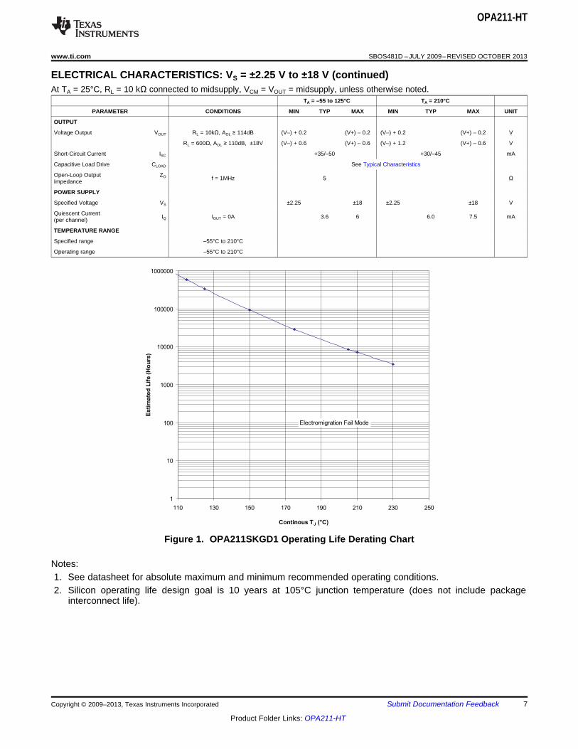
Figure 1. OPA211SKGD1 Operating Life Derating Chart
Notes:1. See datasheet for absolute maximum and minimum recommended operating conditions.2. Silicon operating life design goal is 10 years at 105°C junction temperature (does not include package
interconnect life).
Copyright © 2009–2013, Texas Instruments Incorporated Submit Documentation Feedback 7
Product Folder Links: OPA211-HT
20nV
/div
Time (1s/div)
Tota
l H
arm
on
ic D
isto
rtio
n +
No
ise
(%
)
10
0.001
0.00001
Frequency (Hz)
20k
0.0001
100 1k 10k
V = 15V
R = 600
±
W
S
L
G = 1G = 1-
V = 3VOUT RMSV = 3VOUT RMS
Tota
l Ha
rmo
nic
Dis
tortio
n +
No
ise
(dB
)-100
-140
-120
G = 11
V = 3VOUT RMS
Tota
l H
arm
onic
Dis
tort
ion +
Nois
e (
%)
0.01
0.1
0.000001
Output Voltage Amplitude (V )RMS
100
0.00001
0.1 1 10
0.0001
0.001
0.01
V = 15V
R = 600
1kHz Signal
S
L
±
W
-60
-160
-140
-120
-100
-80
Tota
l Harm
onic
Dis
tortio
n +
Nois
e (d
B)
G = 1
G = 11
G = 1-
Voltage N
ois
e D
ensity (
nV
/)
ÖH
z
0.1
100
1
Frequency (Hz)
100k101
10
100 1k 10k
Cu
rre
nt
No
ise
De
nsity (
pA
/)
ÖH
z
0.1
100
10
1
Frequency (Hz)
100k101 100 1k 10k
OPA211-HT
SBOS481D –JULY 2009–REVISED OCTOBER 2013 www.ti.com
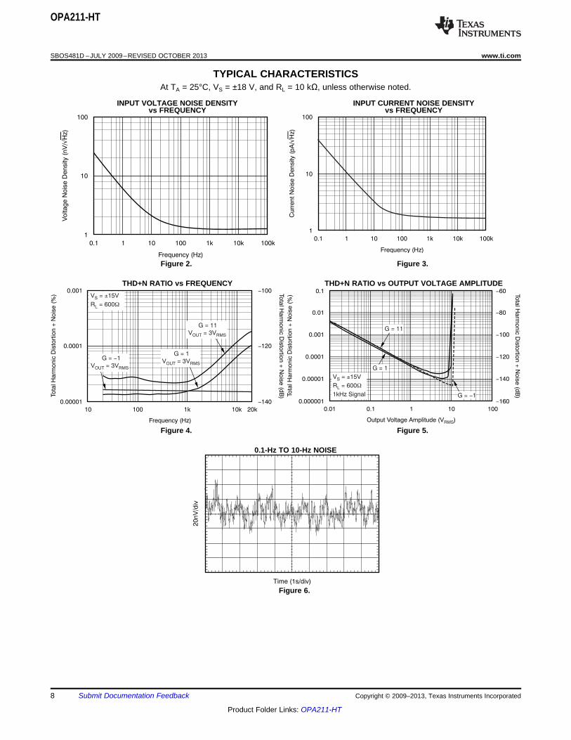
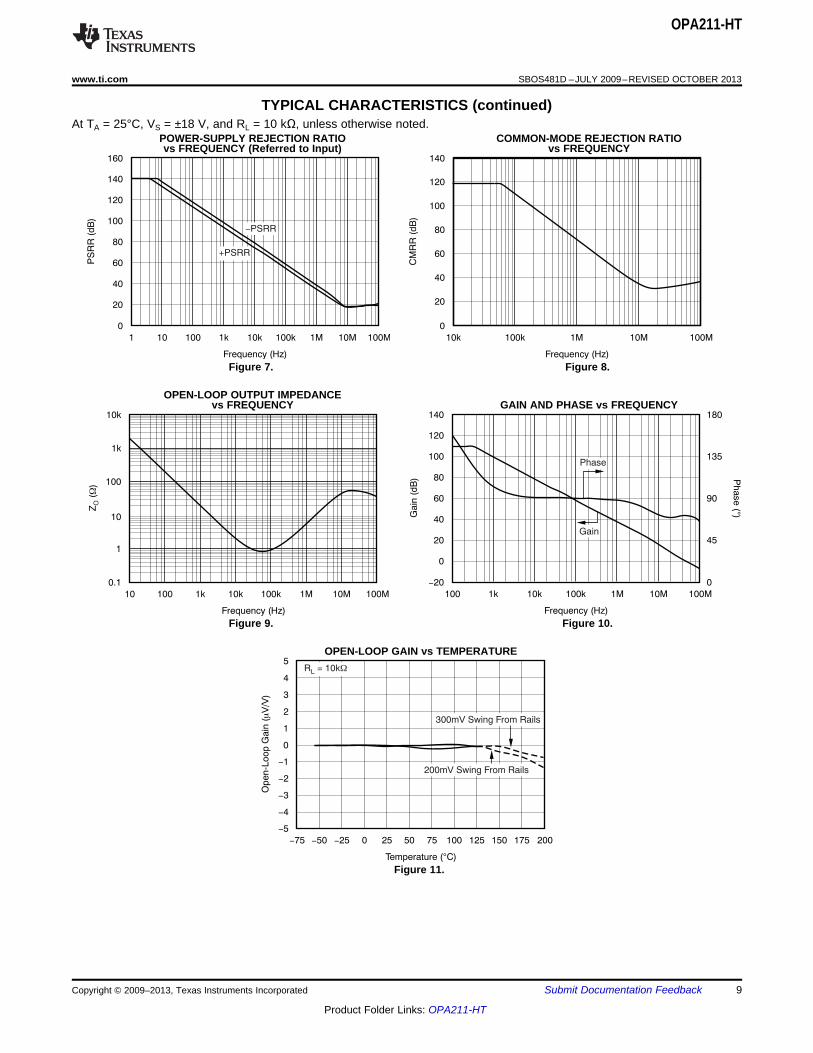
TYPICAL CHARACTERISTICSAt TA = 25°C, VS = ±18 V, and RL = 10 kΩ, unless otherwise noted.
INPUT VOLTAGE NOISE DENSITY INPUT CURRENT NOISE DENSITYvs FREQUENCY vs FREQUENCY
Figure 2. Figure 3.
THD+N RATIO vs FREQUENCY THD+N RATIO vs OUTPUT VOLTAGE AMPLITUDE
Figure 4. Figure 5.
0.1-Hz TO 10-Hz NOISE
Figure 6.
8 Submit Documentation Feedback Copyright © 2009–2013, Texas Instruments Incorporated
Product Folder Links: OPA211-HT
Open-L
oop G
ain
(V
/V)
m
-75
5
-5
Temperature ( C)°
200
2
-50 -25 0
3
4
25 7550
1
100 125 150 175
0
-1
-2
-3
-4
300mV Swing From Rails
200mV Swing From Rails
R = 10kWL
Z(
)W
O
10
10k
0.1
Frequency (Hz)
100M
1
100 1k 10k
10
100
1k
100k 10M1M
Gain
(dB
)
100 1k
140
120
100
80
60
40
-20
Frequency (Hz)
100M1M10k 100k 10M
20
0
Phase (
)°
180
135
90
45
0
Gain
Phase
PS
RR
(dB
)
1 10
160
140
100
80
60
40
0
Frequency (Hz)
100M10k100 1k 100k
20
120
1M 10M
-PSRR
+PSRR
CM
RR
(dB
)
10k
140
100
80
60
40
0
Frequency (Hz)
100M1M100k
20
120
10M
OPA211-HT
www.ti.com SBOS481D –JULY 2009–REVISED OCTOBER 2013
TYPICAL CHARACTERISTICS (continued)At TA = 25°C, VS = ±18 V, and RL = 10 kΩ, unless otherwise noted.
POWER-SUPPLY REJECTION RATIO COMMON-MODE REJECTION RATIOvs FREQUENCY (Referred to Input) vs FREQUENCY
Figure 7. Figure 8.
OPEN-LOOP OUTPUT IMPEDANCEvs FREQUENCY GAIN AND PHASE vs FREQUENCY
Figure 9. Figure 10.
OPEN-LOOP GAIN vs TEMPERATURE
Figure 11.
Copyright © 2009–2013, Texas Instruments Incorporated Submit Documentation Feedback 9
Product Folder Links: OPA211-HT
VS
hift (
V)
mO
S
0
12
-12
Time (s)
60
4
10 20 30
6
8
1020 Typical Units Shown
2
0
-2
-4
-6
-8
-10
40 50
I(n
A)
OS
2.25
100
-100
V ( V)±S
18
20
4 6
40
60
80
8 10 12 14 16
0
-20
-40
-60
-80
5 Typical Units Shown
2000
1500
1000
500
0
-500
-1000
-1500
-2000(V )+1.0- (V )+1.5- (V )+2.0- (V+) 1.5- (V+) 1.0- (V+) 0.5-
V (V)CM
V(
V)
mO
S
Iand I
Bia
s C
urr
ent (n
A)
BO
S
-50
200
150
100
50
0
50
100
150
200
-
-
-
-
Ambient Temperature ( C)°
150-25 0 25
IOS
+IB
50 10075 125
-IB
-125.0
-112.5
-100.0
-75.0
-62.5
-50.0
-37.5
-25.0
-12.5 0
12.5
25.0
37.5
50.0
62.5
75.0
87.5
100.0
112.5
125.0
Offset Voltage ( V)m
Popula
tion
-87.5 0 0.1 0.2 0.3 0.4 0.5 0.6 0.7 0.8 0.9 1.0 1.1 1.2 1.3 1.4 1.5
Offset Voltage Drift (mV/°C)
Popula
tion
OPA211-HT
SBOS481D –JULY 2009–REVISED OCTOBER 2013 www.ti.com
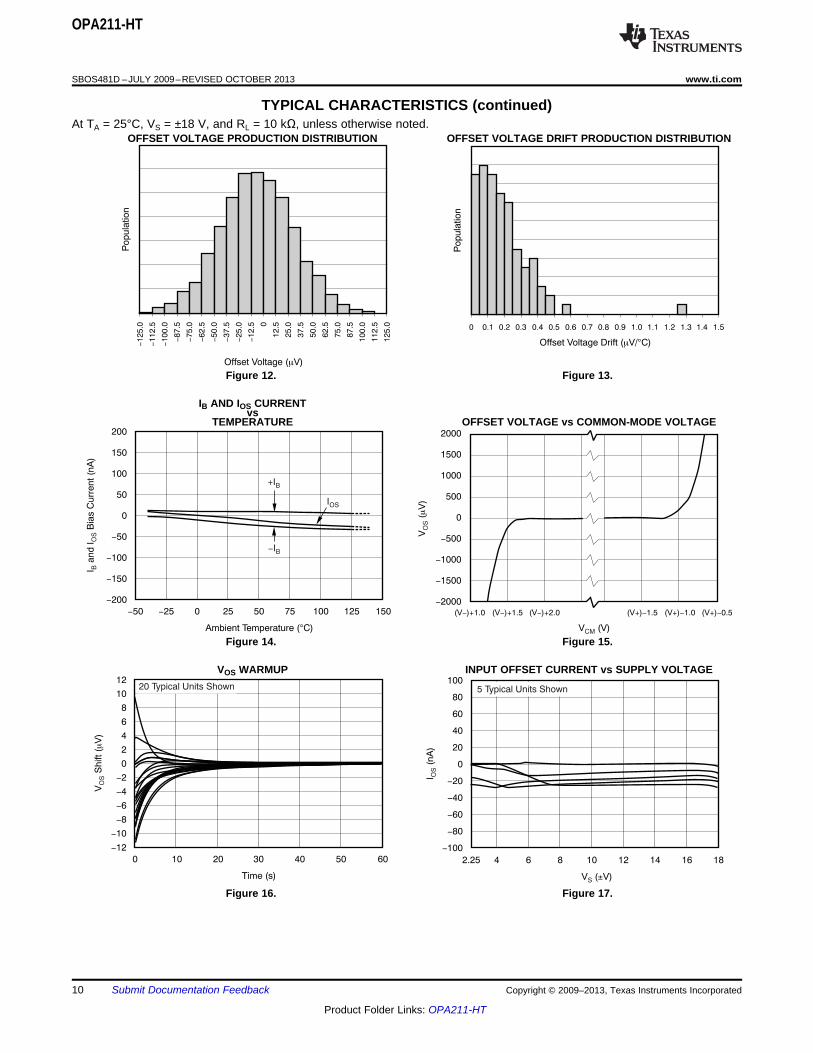
TYPICAL CHARACTERISTICS (continued)At TA = 25°C, VS = ±18 V, and RL = 10 kΩ, unless otherwise noted.
OFFSET VOLTAGE PRODUCTION DISTRIBUTION OFFSET VOLTAGE DRIFT PRODUCTION DISTRIBUTION
Figure 12. Figure 13.
IB AND IOS CURRENTvs
TEMPERATURE OFFSET VOLTAGE vs COMMON-MODE VOLTAGE
Figure 14. Figure 15.
VOS WARMUP INPUT OFFSET CURRENT vs SUPPLY VOLTAGE
Figure 16. Figure 17.
10 Submit Documentation Feedback Copyright © 2009–2013, Texas Instruments Incorporated
Product Folder Links: OPA211-HT

IS
hift (m
A)
Q
0
0.05
-0.30
Time (s)
600
-0.15
60 120 180
-0.10
-0.05
0
240 360300
-0.20
-0.25
420 480 540
Average of 10 Typical Units
I(m
A)
Q
0
4.0
0
V (V)S
36
2.0
4 8 12
2.5
3.0
3.5
16 2420
1.5
1.0
0.5
28 32
I(n
A)
B
1
150
-150
V (V)CM
355 10
100
15 20 25 30
0
-100
50
-50
Common-Mode Range
-IB
+IB
Unit 1 Unit 2
Unit 3
V = 36V
3 Typical Units ShownS
I(m
A)
Q
-75
6
0
Temperature ( C)°
200
2
-50 -25 0
3
4
5
25 7550
1
100 125 150 175
I(n
A)
OS
1
100
-100
V (V)CM
35
75
5 10 15 20 25 30
0
-75
50
25
-25
-50
Common-Mode Range
V = 36V
3 Typical Units ShownS
I(n
A)
B
2.25
150
-150
V ( V)±S
184 6
100
8 10
50
12 14 16
-IB
+IB
Unit 1 Unit 2
Unit 3
3 Typical Units Shown
0
-50
-100
OPA211-HT
www.ti.com SBOS481D –JULY 2009–REVISED OCTOBER 2013
TYPICAL CHARACTERISTICS (continued)At TA = 25°C, VS = ±18 V, and RL = 10 kΩ, unless otherwise noted.
INPUT OFFSET CURRENT vs COMMON-MODE VOLTAGE INPUT BIAS CURRENT vs SUPPLY VOLTAGE
Figure 18. Figure 19.
INPUT BIAS CURRENT vs COMMON-MODE VOLTAGE QUIESCENT CURRENT vs TEMPERATURE
Figure 20. Figure 21.
QUIESCENT CURRENT vs NORMALIZED QUIESCENT CURRENTSUPPLY VOLTAGE vs TIME
Figure 22. Figure 23.
Copyright © 2009–2013, Texas Instruments Incorporated Submit Documentation Feedback 11
Product Folder Links: OPA211-HT
Overs
hoot (%
)
0 200
60
50
40
30
20
10
0
Capacitive Load (pF)
1400800400 600 1000 1200
G = +1
G = 1-
G = 1020m
V/d
iv
Time (0.1 s/div)m
G = +1
R = 600
C = 100pFL W
L
+18V
-18V CLRL
OPA211
20m
V/d
iv
Time (0.1 s/div)m
G = 1
C = 100pF
-
L
+18V
-18V
RF
604W
RI
604W
CF
5.6pF
CL
OPA211
20m
V/d
iv
Time (0.1 s/div)m
G = +1
R = 600
C = 10pFL W
L
+18V
-18V CLRL
OPA211
I(m
A)
SC
-75
60
-60
Temperature ( C)°
200
20
-50 -25 0
30
40
50
25 7550
10
0
-10
100 125
-20
-30
-40
-50
150 175
Sourcing
Sinking
20m
V/d
iv
Time (0.1 s/div)m
G = 1
C = 10pF
-
L
+18V
-18V
RF
604W
RI
604W
CF
5.6pF
CL
OPA211
OPA211-HT
SBOS481D –JULY 2009–REVISED OCTOBER 2013 www.ti.com
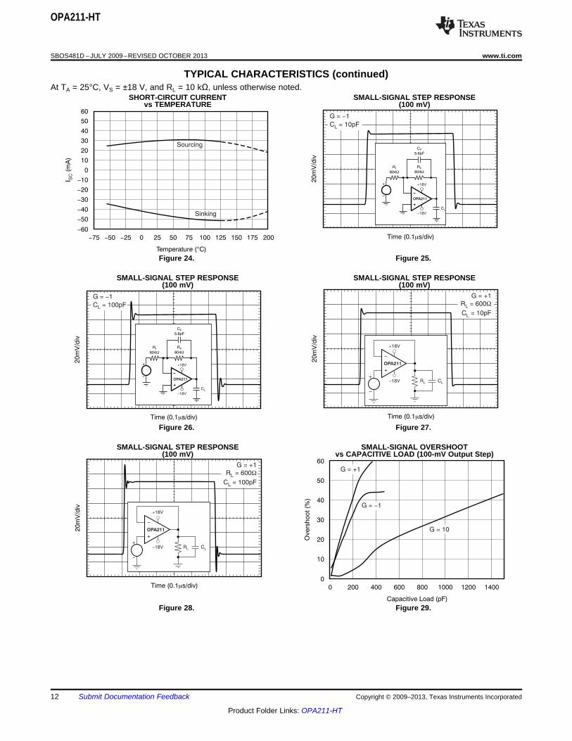
TYPICAL CHARACTERISTICS (continued)At TA = 25°C, VS = ±18 V, and RL = 10 kΩ, unless otherwise noted.
SHORT-CIRCUIT CURRENT SMALL-SIGNAL STEP RESPONSEvs TEMPERATURE (100 mV)
Figure 24. Figure 25.
SMALL-SIGNAL STEP RESPONSE SMALL-SIGNAL STEP RESPONSE(100 mV) (100 mV)
Figure 26. Figure 27.
SMALL-SIGNAL STEP RESPONSE SMALL-SIGNAL OVERSHOOT(100 mV) vs CAPACITIVE LOAD (100-mV Output Step)
Figure 28. Figure 29.
12 Submit Documentation Feedback Copyright © 2009–2013, Texas Instruments Incorporated
Product Folder Links: OPA211-HT
0 100 200 300 400 500 1000600 700 800 900
Time (ns)
1.0
0.8
0.6
0.4
0.2
0
-0.2
-0.4
-0.6
-0.8
-1.0
DF
rom
Fin
al V
alu
e (
mV
)
0.010
0.008
0.006
0.004
0.002
0
-0.002
-0.004
-0.006
-0.008
-0.010
DF
rom
Fin
al V
alu
e (%
)
16-Bit Settling
( 1/2 LSB = 0.00075%)± ±
0 100 200 300 400 500 1000600 700 800 900
Time (ns)
1.0
0.8
0.6
0.4
0.2
0
-0.2
-0.4
-0.6
-0.8
-1.0
Dro
m F
inal V
Falu
e (
mV
)
0.010
0.008
0.006
0.004
0.002
0
-0.002
-0.004
-0.006
-0.008
-0.010
DF
rom
Fin
al V
alu
e (%
)
16-Bit Settling
( 1/2 LSB = 0.00075%)± ±
0 100 200 300 400 500 1000600 700 800 900
Time (ns)
1.0
0.8
0.6
0.4
0.2
0
-0.2
-0.4
-0.6
-0.8
-1.0
DF
rom
Fin
al V
alu
e (
mV
)
0.010
0.008
0.006
0.004
0.002
0
-0.002
-0.004
-0.006
-0.008
-0.010
DF
rom
Fin
al V
alu
e (%
)
16-Bit Settling
( 1/2 LSB = 0.00075%)± ±
0 100 200 300 400 500 1000600 700 800 900
Time (ns)
1.0
0.8
0.6
0.4
0.2
0
-0.2
-0.4
-0.6
-0.8
-1.0
DF
rom
Fin
al V
alu
e (
mV
)
0.010
0.008
0.006
0.004
0.002
0
-0.002
-0.004
-0.006
-0.008
-0.010
DF
rom
Fin
al V
alu
e (%
)
16-Bit Settling
( 1/2 LSB = 0.00075%)± ±
2V
/div
Time (0.5 s/div)m
G = 1
C = 100pF
R = 600
-
W
L
L
2V
/div
Time (0.5 s/div)m
G = +1
C = 100pF
R = 600L
L W
R = 100WF
R = 0WF
Note: See the
section, .
Applications Information
Input Protection
OPA211-HT
www.ti.com SBOS481D –JULY 2009–REVISED OCTOBER 2013
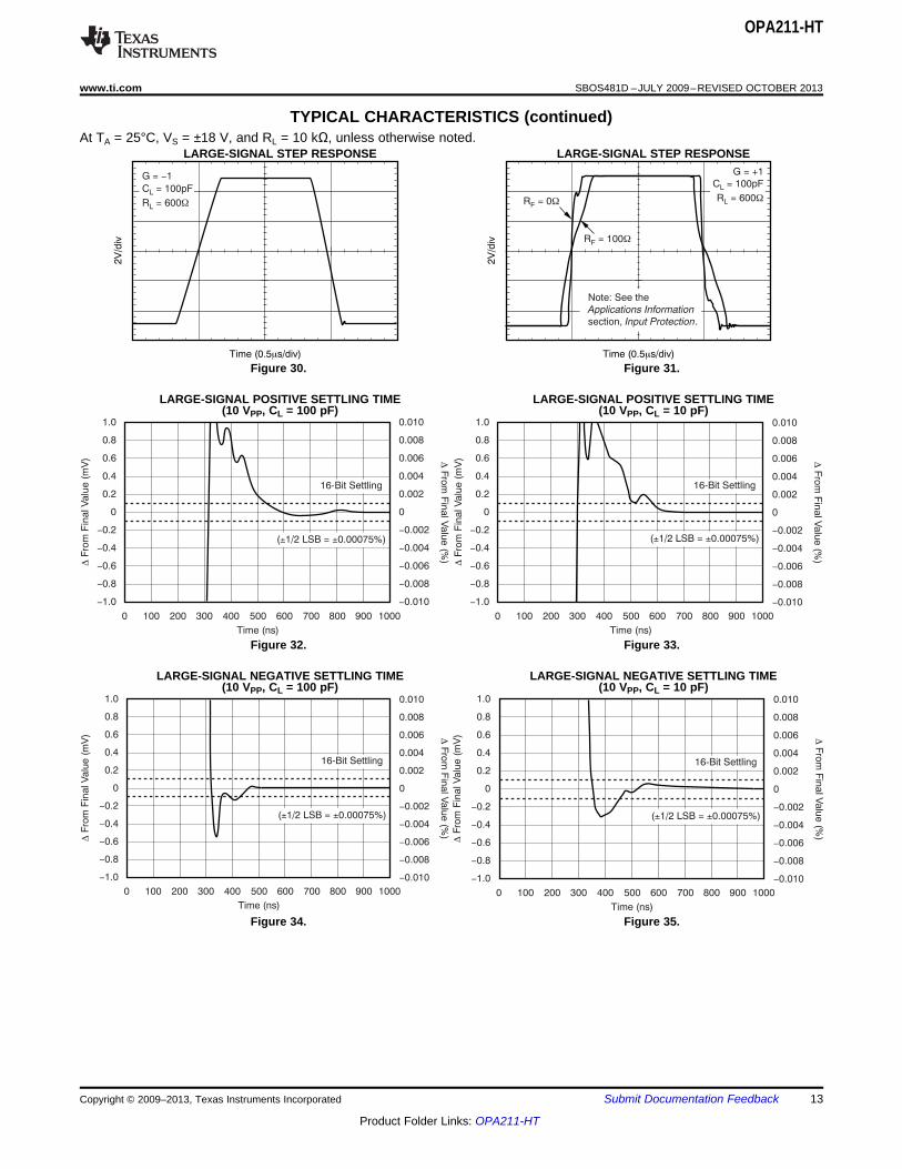
TYPICAL CHARACTERISTICS (continued)At TA = 25°C, VS = ±18 V, and RL = 10 kΩ, unless otherwise noted.
LARGE-SIGNAL STEP RESPONSE LARGE-SIGNAL STEP RESPONSE
Figure 30. Figure 31.
LARGE-SIGNAL POSITIVE SETTLING TIME LARGE-SIGNAL POSITIVE SETTLING TIME(10 VPP, CL = 100 pF) (10 VPP, CL = 10 pF)
Figure 32. Figure 33.
LARGE-SIGNAL NEGATIVE SETTLING TIME LARGE-SIGNAL NEGATIVE SETTLING TIME(10 VPP, CL = 100 pF) (10 VPP, CL = 10 pF)
Figure 34. Figure 35.
Copyright © 2009–2013, Texas Instruments Incorporated Submit Documentation Feedback 13
Product Folder Links: OPA211-HT

5V
/div
20
15
10
5
0
5
10
15
20
-
-
-
-
Time (2 s/div)m
Shutdown Signal
Output Signal
V = 15V±S
5V
/div
20
15
10
5
0
5
10
15
20
-
-
-
-
Time (2 s/div)m
Shutdown Signal
Output Signal
V = 15V±S
0 10 20 30 40 50 7060
I (mA)OUT
20
15
10
5
0
-5
-10
-15
-20
V(V
)O
UT
+125 C°
0 C°
+85 C°
+125 C°
+85 C°
+150 C°- °55 C 0 C°
5V
/div
0.5ms/div
Output
+18V
-18V37VPP
( 18.5V)±
OutputOPA211
5V
/div
Time (0.5 s/div)m
0V
VIN
VOUT
G = 10-
1kW
10kW
VIN
VOUTOPA211
5V
/div
Time (0.5 s/div)m
0V
VIN
VOUT
G = 10-
1kW
10kW
VIN
VOUTOPA211
OPA211-HT
SBOS481D –JULY 2009–REVISED OCTOBER 2013 www.ti.com
TYPICAL CHARACTERISTICS (continued)At TA = 25°C, VS = ±18 V, and RL = 10 kΩ, unless otherwise noted.
NEGATIVE OVERLOAD RECOVERY POSITIVE OVERLOAD RECOVERY
Figure 36. Figure 37.
OUTPUT VOLTAGE vs OUTPUT CURRENT NO PHASE REVERSAL
Figure 38. Figure 39.
TURN-OFF TRANSIENT TURN-ON TRANSIENT
Figure 40. Figure 41.
14 Submit Documentation Feedback Copyright © 2009–2013, Texas Instruments Incorporated
Product Folder Links: OPA211-HT
Shutd
ow
n P
in V
oltage (
V)
20
15
10
5
0
5
10
15
20
-
-
-
-
Time (100 s/div)m
Shutdown Signal
Outp
ut V
olta
ge (V
)
1.6
1.2
0.8
0.4
0
0.4
0.8
1.2
1.6
-
-
-
-
Output
V = 15V±S
OPA211-HT
www.ti.com SBOS481D –JULY 2009–REVISED OCTOBER 2013
TYPICAL CHARACTERISTICS (continued)At TA = 25°C, VS = ±18 V, and RL = 10 kΩ, unless otherwise noted.
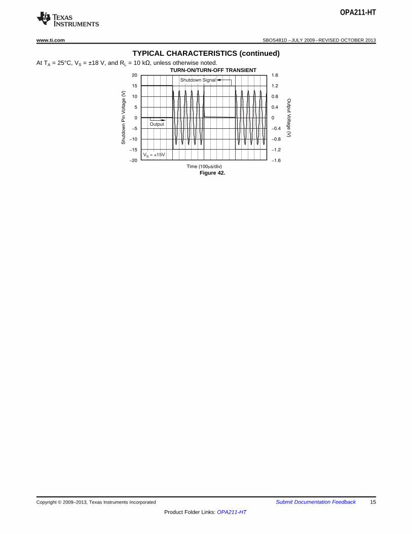
TURN-ON/TURN-OFF TRANSIENT
Figure 42.
Copyright © 2009–2013, Texas Instruments Incorporated Submit Documentation Feedback 15
Product Folder Links: OPA211-HT
IN-
Pre-Output Driver OUT
IN+
V-
V+
OPA211-HT
SBOS481D –JULY 2009–REVISED OCTOBER 2013 www.ti.com
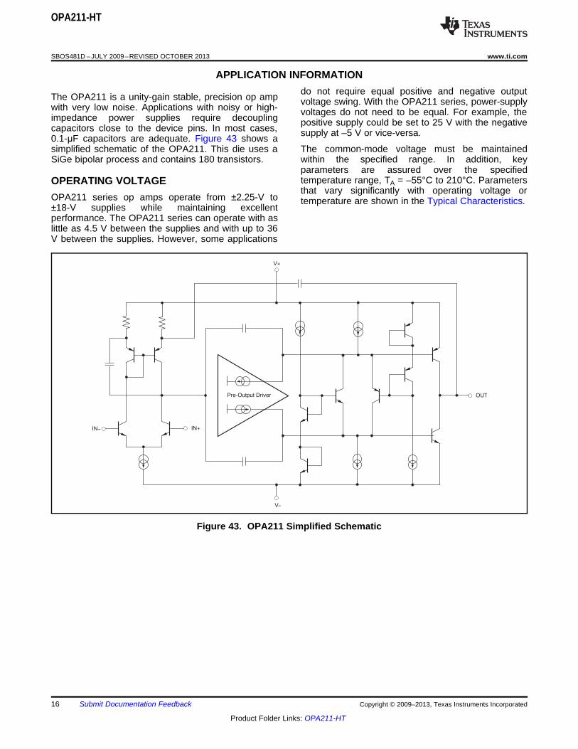
APPLICATION INFORMATIONdo not require equal positive and negative outputThe OPA211 is a unity-gain stable, precision op amp voltage swing. With the OPA211 series, power-supplywith very low noise. Applications with noisy or high- voltages do not need to be equal. For example, theimpedance power supplies require decoupling positive supply could be set to 25 V with the negativecapacitors close to the device pins. In most cases, supply at –5 V or vice-versa.0.1-μF capacitors are adequate. Figure 43 shows a
simplified schematic of the OPA211. This die uses a The common-mode voltage must be maintainedSiGe bipolar process and contains 180 transistors. within the specified range. In addition, key
parameters are assured over the specifiedtemperature range, TA = –55°C to 210°C. ParametersOPERATING VOLTAGEthat vary significantly with operating voltage or
OPA211 series op amps operate from ±2.25-V to temperature are shown in the Typical Characteristics.±18-V supplies while maintaining excellentperformance. The OPA211 series can operate with aslittle as 4.5 V between the supplies and with up to 36V between the supplies. However, some applications
Figure 43. OPA211 Simplified Schematic
16 Submit Documentation Feedback Copyright © 2009–2013, Texas Instruments Incorporated
Product Folder Links: OPA211-HT
OPA211 Output
RF
Input
-
+RI
VOLTAGE NOISE SPECTRAL DENSITY
vs SOURCE RESISTANCE
100k 1M
Source Resistance, R ( )WS
100 1k 10k
10k
1k
100
10
1
Votlage N
ois
e S
pectr
al D
ensity,
EO
RS
EO
E = eO n S+ (i R ) + 4kTRn S
2 2 2
Resistor Noise
OPA227
OPA211
OPA211-HT
www.ti.com SBOS481D –JULY 2009–REVISED OCTOBER 2013
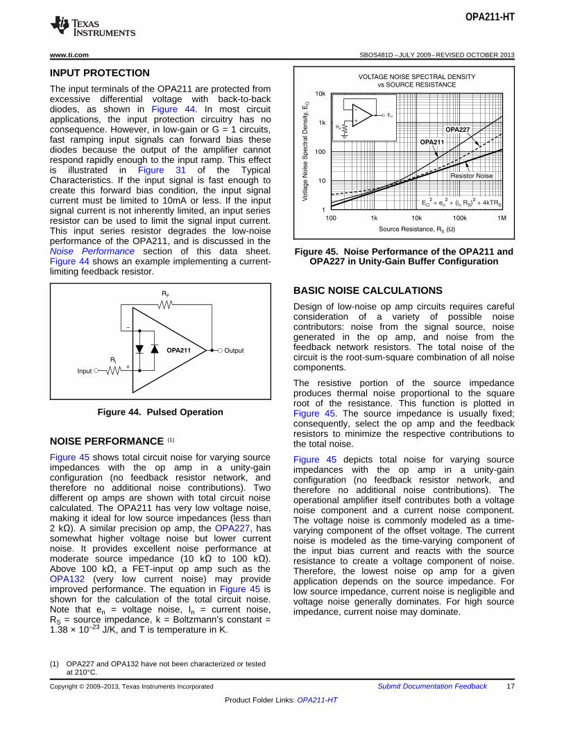
INPUT PROTECTIONThe input terminals of the OPA211 are protected fromexcessive differential voltage with back-to-backdiodes, as shown in Figure 44. In most circuitapplications, the input protection circuitry has noconsequence. However, in low-gain or G = 1 circuits,fast ramping input signals can forward bias thesediodes because the output of the amplifier cannotrespond rapidly enough to the input ramp. This effectis illustrated in Figure 31 of the TypicalCharacteristics. If the input signal is fast enough tocreate this forward bias condition, the input signalcurrent must be limited to 10mA or less. If the inputsignal current is not inherently limited, an input seriesresistor can be used to limit the signal input current.This input series resistor degrades the low-noiseperformance of the OPA211, and is discussed in theNoise Performance section of this data sheet. Figure 45. Noise Performance of the OPA211 andFigure 44 shows an example implementing a current- OPA227 in Unity-Gain Buffer Configurationlimiting feedback resistor.
BASIC NOISE CALCULATIONSDesign of low-noise op amp circuits requires carefulconsideration of a variety of possible noisecontributors: noise from the signal source, noisegenerated in the op amp, and noise from thefeedback network resistors. The total noise of thecircuit is the root-sum-square combination of all noisecomponents.
The resistive portion of the source impedanceproduces thermal noise proportional to the squareroot of the resistance. This function is plotted in
Figure 44. Pulsed Operation Figure 45. The source impedance is usually fixed;consequently, select the op amp and the feedbackresistors to minimize the respective contributions to
NOISE PERFORMANCE (1) the total noise.Figure 45 shows total circuit noise for varying source Figure 45 depicts total noise for varying sourceimpedances with the op amp in a unity-gain impedances with the op amp in a unity-gainconfiguration (no feedback resistor network, and configuration (no feedback resistor network, andtherefore no additional noise contributions). Two therefore no additional noise contributions). Thedifferent op amps are shown with total circuit noise operational amplifier itself contributes both a voltagecalculated. The OPA211 has very low voltage noise, noise component and a current noise component.making it ideal for low source impedances (less than The voltage noise is commonly modeled as a time-2 kΩ). A similar precision op amp, the OPA227, has varying component of the offset voltage. The currentsomewhat higher voltage noise but lower current noise is modeled as the time-varying component ofnoise. It provides excellent noise performance at the input bias current and reacts with the sourcemoderate source impedance (10 kΩ to 100 kΩ). resistance to create a voltage component of noise.Above 100 kΩ, a FET-input op amp such as the Therefore, the lowest noise op amp for a givenOPA132 (very low current noise) may provide application depends on the source impedance. Forimproved performance. The equation in Figure 45 is low source impedance, current noise is negligible andshown for the calculation of the total circuit noise. voltage noise generally dominates. For high sourceNote that en = voltage noise, In = current noise, impedance, current noise may dominate.RS = source impedance, k = Boltzmann’s constant =1.38 × 10⁻²³ J/K, and T is temperature in K.
(1) OPA227 and OPA132 have not been characterized or testedat 210°C.
Copyright © 2009–2013, Texas Instruments Incorporated Submit Documentation Feedback 17
Product Folder Links: OPA211-HT
OPA211-HT
SBOS481D –JULY 2009–REVISED OCTOBER 2013 www.ti.com
Figure 46 illustrates both inverting and noninverting 101, thus extending the resolution by 101. Note thatop amp circuit configurations with gain. In circuit the input signal and load applied to the op amp areconfigurations with gain, the feedback network the same as with conventional feedback without R3.resistors also contribute noise. The current noise of The value of R3 should be kept small to minimize itsthe op amp reacts with the feedback resistors to effect on the distortion measurements.create additional noise components. The feedback Validity of this technique can be verified byresistor values can generally be chosen to make duplicating measurements at high gain and/or highthese noise sources negligible. The equations for frequency where the distortion is within thetotal noise are shown for both configurations. measurement capability of the test equipment.
Measurements for this data sheet were made with anTOTAL HARMONIC DISTORTION Audio Precision System Two distortion/noiseMEASUREMENTS analyzer, which greatly simplifies such repetitivemeasurements. The measurement technique can,OPA211 series op amps have excellent distortionhowever, be performed with manual distortioncharacteristics. THD + Noise is below 0.0001%measurement instruments.(G = 1, VO = 3 VRMS) throughout the audio frequency
range, 20 Hz to 20 kHz, with a 600-Ω load.SHUTDOWNThe distortion produced by OPA211 series op amps
is below the measurement limit of many commercially The shutdown (enable) function of the OPA211 isavailable distortion analyzers. However, a special test referenced to the positive supply voltage of thecircuit illustrated in Figure 47 can be used to extend operational amplifier. A valid high disables the opthe measurement capabilities. amp. A valid high is defined as (V+) – 0.35 V of the
positive supply applied to the shutdown pin. A validOp amp distortion can be considered an internal error low is defined as (V+) – 3 V below the positive supplysource that can be referred to the input. Figure 47 pin. For example, with VCC at ±15 V, the device isshows a circuit that causes the op amp distortion to enabled at or below 12 V. The device is disabled atbe 101 times greater than that normally produced by or above 14.65 V. If dual or split power supplies arethe op amp. The addition of R3 to the otherwise used, care should be taken to ensure the valid highstandard noninverting amplifier configuration alters or valid low input signals are properly referred to thethe feedback factor or noise gain of the circuit. The positive supply voltage. This pin must be connectedclosed-loop gain is unchanged, but the feedback to a valid high or low voltage or driven, and not leftavailable for error correction is reduced by a factor of open-circuit. The enable and disable times areprovided in the Typical Characteristics section (seeFigure 40 through Figure 42). When disabled, theoutput assumes a high-impedance state.
18 Submit Documentation Feedback Copyright © 2009–2013, Texas Instruments Incorporated
Product Folder Links: OPA211-HT

R2
OPA211
R1
Signal Gain = 1+
Distortion Gain = 1+
R3 VOUT
Generator
Output
Analyzer
Input
Audio Precision
System Two(1)
with PC Controller
Load
SIG.
GAIN
DIST.
GAIN R1
R2
R3
¥
100W
1kW
1kW
10W
11W
1
11
101
101R2
R1
R2
R II R1 3
R1
R2
EO
R1
R2
EORS
VS
RS
VS
Noise in Noninverting Gain Configuration
Noise in Inverting Gain Configuration
Noise at the output:
E =O
2
Where e = ÖS S4kTR ´ = thermal noise of RS
2
1 +R2
R1
e + en 1 2 n 2 S S+ e + (i R ) + e + (i
nR )
2 2 2 2 2 2
1 +R2
R1
R2
R1
e = Ö1 14kTR ´ = thermal noise of R1
2
1 +R2
R1
e = Ö2 2 24kTR = thermal noise of R
Noise at the output:
E =O
2
Where e = 4kTRÖS S ´ = thermal noise of RS
2
1 +R2
R + R1 S
e + en 1 2 n 2 S+ e + (i R ) + e2 2 2 2 2
R2
R + R1 S
R2
R + R1 S
e = 4kTRÖ1 1 ´ = thermal noise of R1
e = 4kTRÖ2 2 2= thermal noise of R
For the OPA211 series op amps at 1kHz, e = 1.1nV/ Hz and i = 1.7pA/ Hz.Ö Ön n
OPA211-HT
www.ti.com SBOS481D –JULY 2009–REVISED OCTOBER 2013
Figure 46. Noise Calculation in Gain Configurations
Figure 47. Distortion Test Circuit
Copyright © 2009–2013, Texas Instruments Incorporated Submit Documentation Feedback 19
Product Folder Links: OPA211-HT
RF
Op-Amp
Core
RI
RL
V(1)
IN
ID
-In
Out
+In
ESD Current-
Steering Diodes
Edge-Triggered ESD
Absorption Circuit
+VS
+V
-V
-VS
OPA211
OPA211-HT
SBOS481D –JULY 2009–REVISED OCTOBER 2013 www.ti.com
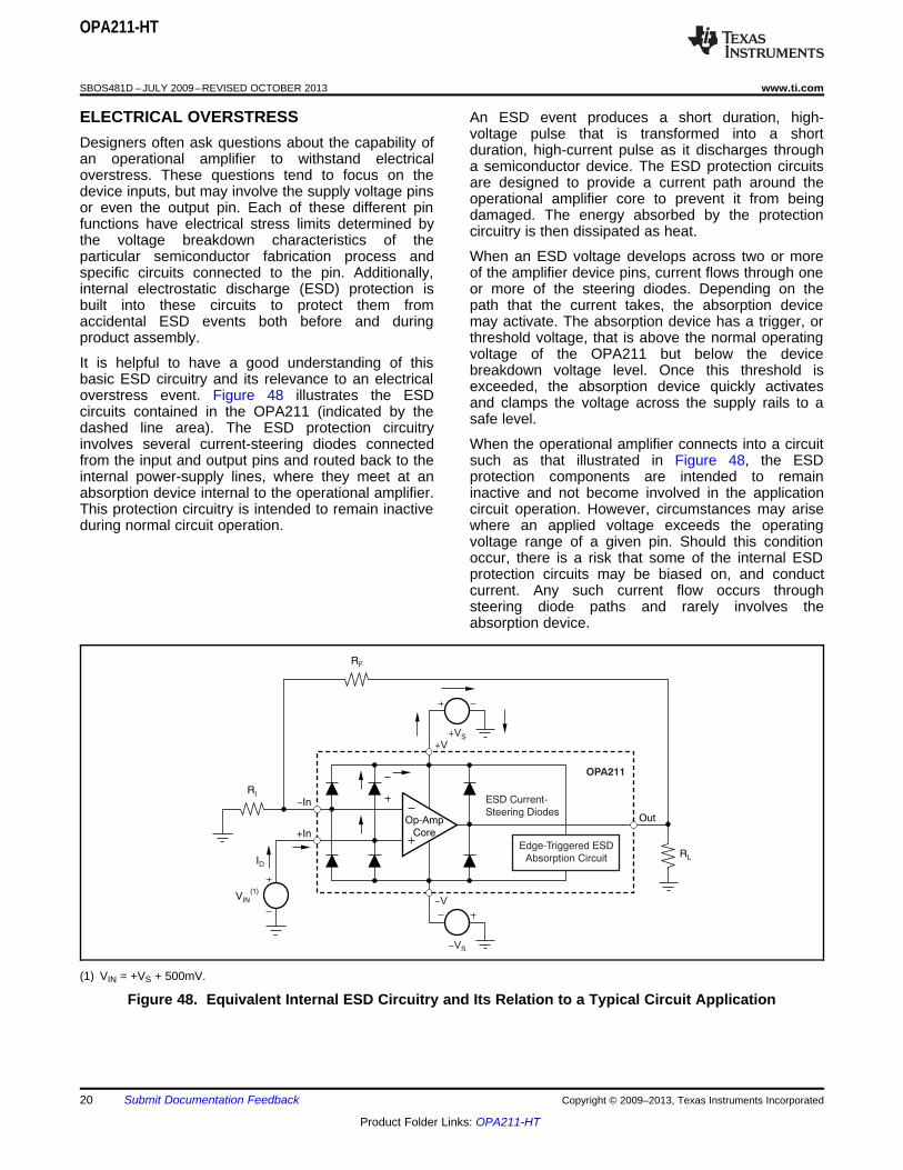
ELECTRICAL OVERSTRESS An ESD event produces a short duration, high-voltage pulse that is transformed into a shortDesigners often ask questions about the capability of duration, high-current pulse as it discharges throughan operational amplifier to withstand electrical a semiconductor device. The ESD protection circuitsoverstress. These questions tend to focus on the are designed to provide a current path around thedevice inputs, but may involve the supply voltage pins operational amplifier core to prevent it from beingor even the output pin. Each of these different pin damaged. The energy absorbed by the protectionfunctions have electrical stress limits determined by circuitry is then dissipated as heat.the voltage breakdown characteristics of the
particular semiconductor fabrication process and When an ESD voltage develops across two or morespecific circuits connected to the pin. Additionally, of the amplifier device pins, current flows through oneinternal electrostatic discharge (ESD) protection is or more of the steering diodes. Depending on thebuilt into these circuits to protect them from path that the current takes, the absorption deviceaccidental ESD events both before and during may activate. The absorption device has a trigger, orproduct assembly. threshold voltage, that is above the normal operating
voltage of the OPA211 but below the deviceIt is helpful to have a good understanding of this breakdown voltage level. Once this threshold isbasic ESD circuitry and its relevance to an electrical exceeded, the absorption device quickly activatesoverstress event. Figure 48 illustrates the ESD and clamps the voltage across the supply rails to acircuits contained in the OPA211 (indicated by the safe level.dashed line area). The ESD protection circuitryinvolves several current-steering diodes connected When the operational amplifier connects into a circuitfrom the input and output pins and routed back to the such as that illustrated in Figure 48, the ESDinternal power-supply lines, where they meet at an protection components are intended to remainabsorption device internal to the operational amplifier. inactive and not become involved in the applicationThis protection circuitry is intended to remain inactive circuit operation. However, circumstances may ariseduring normal circuit operation. where an applied voltage exceeds the operating
voltage range of a given pin. Should this conditionoccur, there is a risk that some of the internal ESDprotection circuits may be biased on, and conductcurrent. Any such current flow occurs throughsteering diode paths and rarely involves theabsorption device.
(1) VIN = +VS + 500mV.
Figure 48. Equivalent Internal ESD Circuitry and Its Relation to a Typical Circuit Application
20 Submit Documentation Feedback Copyright © 2009–2013, Texas Instruments Incorporated
Product Folder Links: OPA211-HT
OPA211-HT
www.ti.com SBOS481D –JULY 2009–REVISED OCTOBER 2013
Figure 48 depicts a specific example where the input DFN PACKAGEvoltage, VIN, exceeds the positive supply voltage The OPA211 is offered in an DFN-8 package (also(+VS) by 500 mV or more. Much of what happens in known as SON). The DFN package is a QFNthe circuit depends on the supply characteristics. If VS package with lead contacts on only two sides of thecan sink the current, one of the upper input steering bottom of the package. This leadless packagediodes conducts and directs current to VS. maximizes board space and enhances thermal andExcessively high current levels can flow with electrical characteristics through an exposed pad.increasingly higher VIN. As a result, the datasheetspecifications recommend that applications limit the DFN packages are physically small, and have ainput current to 10 mA. smaller routing area, improved thermal performance,
and improved electrical parasitics. Additionally, theIf the supply is not capable of sinking the current, VIN absence of external leads eliminates bent-leadmay begin sourcing current to the operational issues.amplifier, and then take over as the source of positivesupply voltage. The danger in this case is that the The DFN package can be easily mounted usingvoltage can rise to levels that exceed the operational standard printed circuit board (PCB) assemblyamplifier absolute maximum ratings. In extreme but techniques. See Application Note QFN/SON PCBrare cases, the absorption device triggers on while VS Attachment (SLUA271) and Application Report Quadand –VS are applied. If this event happens, a direct Flatpack No-Lead Logic Packages (SCBA017), bothcurrent path is established between the VS and –VS available for download at www.ti.com.supplies. The power dissipation of the absorption
The exposed leadframe die pad on the bottom ofdevice is quickly exceeded, and the extreme internalthe package must be connected to V–. Solderingheating destroys the operational amplifier.the thermal pad improves heat dissipation and
Another common question involves what happens to enables specified device performance.the amplifier if an input signal is applied to the inputwhile the power supplies VS and/or –VS are at 0 V. DFN LAYOUT GUIDELINESAgain, it depends on the supply characteristic while at
The exposed leadframe die pad on the DFN package0 V, or at a level below the input signal amplitude. Ifshould be soldered to a thermal pad on the PCB. Athe supplies appear as high impedance, then themechanical drawing showing an example layout isoperational amplifier supply current may be suppliedattached at the end of this data sheet. Refinements toby the input source via the current steering diodes.this layout may be necessary based on assemblyThis state is not a normal bias condition; the amplifierprocess requirements. Mechanical drawings locatedmost likely will not operate normally. If the suppliesat the end of this data sheet list the physicalare low impedance, then the current through thedimensions for the package and pad. The five holessteering diodes can become quite high. The currentin the landing pattern are optional, and are intendedlevel depends on the ability of the input source tofor use with thermal vias that connect the leadframedeliver current, and any resistance in the input path.die pad to the heatsink area on the PCB.
Soldering the exposed pad significantly improvesboard-level reliability during temperature cycling, keypush, package shear, and similar board-level tests.Even with applications that have low-powerdissipation, the exposed pad must be soldered to thePCB to provide structural integrity and long-termreliability.
Copyright © 2009–2013, Texas Instruments Incorporated Submit Documentation Feedback 21
Product Folder Links: OPA211-HT
PACKAGE OPTION ADDENDUM
www.ti.com 25-Oct-2016
Addendum-Page 1
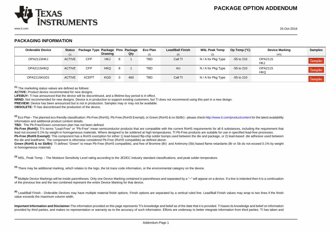
PACKAGING INFORMATION
Orderable Device Status(1)
Package Type PackageDrawing
Pins PackageQty
Eco Plan(2)
Lead/Ball Finish(6)
MSL Peak Temp(3)
Op Temp (°C) Device Marking(4/5)
Samples
OPA211SHKJ ACTIVE CFP HKJ 8 1 TBD Call TI N / A for Pkg Type -55 to 210 OPA211SHKJ
OPA211SHKQ ACTIVE CFP HKQ 8 1 TBD AU N / A for Pkg Type -55 to 210 OPA211SHKQ
OPA211SKGD1 ACTIVE XCEPT KGD 0 400 TBD Call TI N / A for Pkg Type -55 to 210
(1) The marketing status values are defined as follows:ACTIVE: Product device recommended for new designs.LIFEBUY: TI has announced that the device will be discontinued, and a lifetime-buy period is in effect.NRND: Not recommended for new designs. Device is in production to support existing customers, but TI does not recommend using this part in a new design.PREVIEW: Device has been announced but is not in production. Samples may or may not be available.OBSOLETE: TI has discontinued the production of the device.
(2) Eco Plan - The planned eco-friendly classification: Pb-Free (RoHS), Pb-Free (RoHS Exempt), or Green (RoHS & no Sb/Br) - please check http://www.ti.com/productcontent for the latest availabilityinformation and additional product content details.TBD: The Pb-Free/Green conversion plan has not been defined.Pb-Free (RoHS): TI's terms "Lead-Free" or "Pb-Free" mean semiconductor products that are compatible with the current RoHS requirements for all 6 substances, including the requirement thatlead not exceed 0.1% by weight in homogeneous materials. Where designed to be soldered at high temperatures, TI Pb-Free products are suitable for use in specified lead-free processes.Pb-Free (RoHS Exempt): This component has a RoHS exemption for either 1) lead-based flip-chip solder bumps used between the die and package, or 2) lead-based die adhesive used betweenthe die and leadframe. The component is otherwise considered Pb-Free (RoHS compatible) as defined above.Green (RoHS & no Sb/Br): TI defines "Green" to mean Pb-Free (RoHS compatible), and free of Bromine (Br) and Antimony (Sb) based flame retardants (Br or Sb do not exceed 0.1% by weightin homogeneous material)
(3) MSL, Peak Temp. - The Moisture Sensitivity Level rating according to the JEDEC industry standard classifications, and peak solder temperature.
(4) There may be additional marking, which relates to the logo, the lot trace code information, or the environmental category on the device.
(5) Multiple Device Markings will be inside parentheses. Only one Device Marking contained in parentheses and separated by a "~" will appear on a device. If a line is indented then it is a continuationof the previous line and the two combined represent the entire Device Marking for that device.
(6) Lead/Ball Finish - Orderable Devices may have multiple material finish options. Finish options are separated by a vertical ruled line. Lead/Ball Finish values may wrap to two lines if the finishvalue exceeds the maximum column width.
Important Information and Disclaimer:The information provided on this page represents TI's knowledge and belief as of the date that it is provided. TI bases its knowledge and belief on informationprovided by third parties, and makes no representation or warranty as to the accuracy of such information. Efforts are underway to better integrate information from third parties. TI has taken and

PACKAGE OPTION ADDENDUM
www.ti.com 25-Oct-2016
Addendum-Page 2
continues to take reasonable steps to provide representative and accurate information but may not have conducted destructive testing or chemical analysis on incoming materials and chemicals.TI and TI suppliers consider certain information to be proprietary, and thus CAS numbers and other limited information may not be available for release.
In no event shall TI's liability arising out of such information exceed the total purchase price of the TI part(s) at issue in this document sold by TI to Customer on an annual basis.
OTHER QUALIFIED VERSIONS OF OPA211-HT :
• Catalog: OPA211
• Enhanced Product: OPA211-EP
NOTE: Qualified Version Definitions:
• Catalog - TI's standard catalog product
• Enhanced Product - Supports Defense, Aerospace and Medical Applications
IMPORTANT NOTICE
Texas Instruments Incorporated and its subsidiaries (TI) reserve the right to make corrections, enhancements, improvements and otherchanges to its semiconductor products and services per JESD46, latest issue, and to discontinue any product or service per JESD48, latestissue. Buyers should obtain the latest relevant information before placing orders and should verify that such information is current andcomplete. All semiconductor products (also referred to herein as “components”) are sold subject to TI’s terms and conditions of salesupplied at the time of order acknowledgment.TI warrants performance of its components to the specifications applicable at the time of sale, in accordance with the warranty in TI’s termsand conditions of sale of semiconductor products. Testing and other quality control techniques are used to the extent TI deems necessaryto support this warranty. Except where mandated by applicable law, testing of all parameters of each component is not necessarilyperformed.TI assumes no liability for applications assistance or the design of Buyers’ products. Buyers are responsible for their products andapplications using TI components. To minimize the risks associated with Buyers’ products and applications, Buyers should provideadequate design and operating safeguards.TI does not warrant or represent that any license, either express or implied, is granted under any patent right, copyright, mask work right, orother intellectual property right relating to any combination, machine, or process in which TI components or services are used. Informationpublished by TI regarding third-party products or services does not constitute a license to use such products or services or a warranty orendorsement thereof. Use of such information may require a license from a third party under the patents or other intellectual property of thethird party, or a license from TI under the patents or other intellectual property of TI.Reproduction of significant portions of TI information in TI data books or data sheets is permissible only if reproduction is without alterationand is accompanied by all associated warranties, conditions, limitations, and notices. TI is not responsible or liable for such altereddocumentation. Information of third parties may be subject to additional restrictions.Resale of TI components or services with statements different from or beyond the parameters stated by TI for that component or servicevoids all express and any implied warranties for the associated TI component or service and is an unfair and deceptive business practice.TI is not responsible or liable for any such statements.Buyer acknowledges and agrees that it is solely responsible for compliance with all legal, regulatory and safety-related requirementsconcerning its products, and any use of TI components in its applications, notwithstanding any applications-related information or supportthat may be provided by TI. Buyer represents and agrees that it has all the necessary expertise to create and implement safeguards whichanticipate dangerous consequences of failures, monitor failures and their consequences, lessen the likelihood of failures that might causeharm and take appropriate remedial actions. Buyer will fully indemnify TI and its representatives against any damages arising out of the useof any TI components in safety-critical applications.In some cases, TI components may be promoted specifically to facilitate safety-related applications. With such components, TI’s goal is tohelp enable customers to design and create their own end-product solutions that meet applicable functional safety standards andrequirements. Nonetheless, such components are subject to these terms.No TI components are authorized for use in FDA Class III (or similar life-critical medical equipment) unless authorized officers of the partieshave executed a special agreement specifically governing such use.Only those TI components which TI has specifically designated as military grade or “enhanced plastic” are designed and intended for use inmilitary/aerospace applications or environments. Buyer acknowledges and agrees that any military or aerospace use of TI componentswhich have not been so designated is solely at the Buyer's risk, and that Buyer is solely responsible for compliance with all legal andregulatory requirements in connection with such use.TI has specifically designated certain components as meeting ISO/TS16949 requirements, mainly for automotive use. In any case of use ofnon-designated products, TI will not be responsible for any failure to meet ISO/TS16949.
Products ApplicationsAudio www.ti.com/audio Automotive and Transportation www.ti.com/automotiveAmplifiers amplifier.ti.com Communications and Telecom www.ti.com/communicationsData Converters dataconverter.ti.com Computers and Peripherals www.ti.com/computersDLP® Products www.dlp.com Consumer Electronics www.ti.com/consumer-appsDSP dsp.ti.com Energy and Lighting www.ti.com/energyClocks and Timers www.ti.com/clocks Industrial www.ti.com/industrialInterface interface.ti.com Medical www.ti.com/medicalLogic logic.ti.com Security www.ti.com/securityPower Mgmt power.ti.com Space, Avionics and Defense www.ti.com/space-avionics-defenseMicrocontrollers microcontroller.ti.com Video and Imaging www.ti.com/videoRFID www.ti-rfid.comOMAP Applications Processors www.ti.com/omap TI E2E Community e2e.ti.comWireless Connectivity www.ti.com/wirelessconnectivity
Mailing Address: Texas Instruments, Post Office Box 655303, Dallas, Texas 75265Copyright © 2016, Texas Instruments Incorporated