on the hpdp - indico at esa / estec (indico) · worst case process worst case voltage (1.10v) worst...
TRANSCRIPT
On the HPDP from architecture to a device
Final Presentation Days
ESTEC, May 9th 2017
2
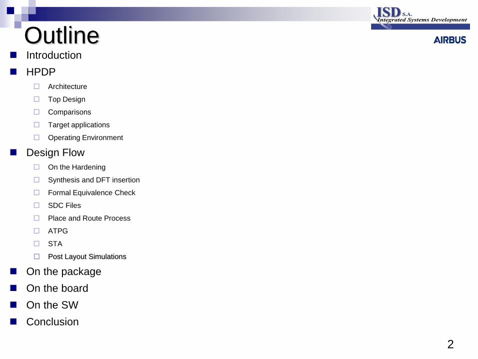
Outline Introduction
HPDP
Architecture
Top Design
Comparisons
Target applications
Operating Environment
Design Flow
On the Hardening
Synthesis and DFT insertion
Formal Equivalence Check
SDC Files
Place and Route Process
ATPG
STA
Post Layout Simulations
On the package
On the board
On the SW
Conclusion
3
Introduction
The development of HPDP has been initiated by the European Space Agency (ESA) and DLR to address the need for a flexible and re-programmable high performance data processor.
It is being implemented in the 65nm radiation hardened technology of ST Microelectronics.
Key Advantages of HPDP device: Ability to meet the increasing requirements of future payloads regarding flexibility, processing power and re-programmability
Ease of inclusion of late changes (customer or mission requirements)
Allowance for the adaptation (changes in standards or in higher protocol layers)
4
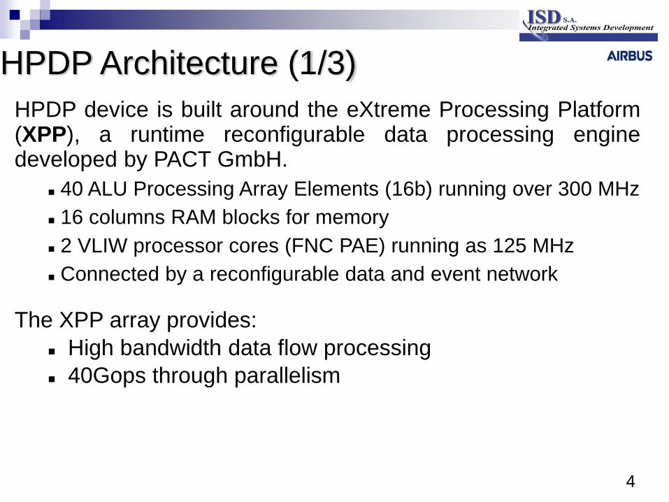
HPDP device is built around the eXtreme Processing Platform (XPP), a runtime reconfigurable data processing engine developed by PACT GmbH.
40 ALU Processing Array Elements (16b) running over 300 MHz
16 columns RAM blocks for memory
2 VLIW processor cores (FNC PAE) running as 125 MHz
Connected by a reconfigurable data and event network
The XPP array provides:
High bandwidth data flow processing
40Gops through parallelism
HPDP Architecture (1/3)
5
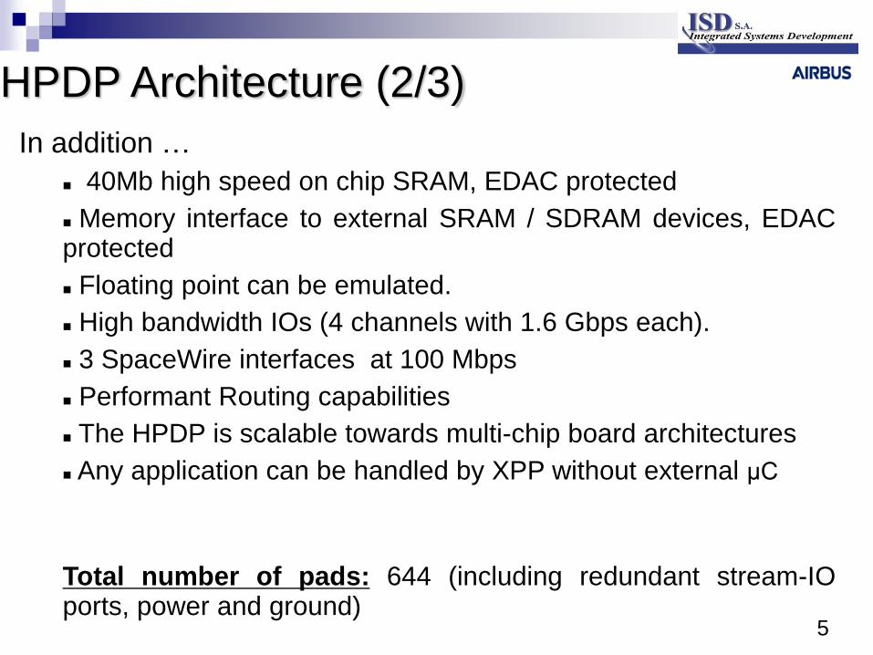
In addition …
40Mb high speed on chip SRAM, EDAC protected
Memory interface to external SRAM / SDRAM devices, EDAC protected
Floating point can be emulated.
High bandwidth IOs (4 channels with 1.6 Gbps each).
3 SpaceWire interfaces at 100 Mbps
Performant Routing capabilities
The HPDP is scalable towards multi-chip board architectures
Any application can be handled by XPP without external μC
Total number of pads: 644 (including redundant stream-IO ports, power and ground)
HPDP Architecture (2/3)
6
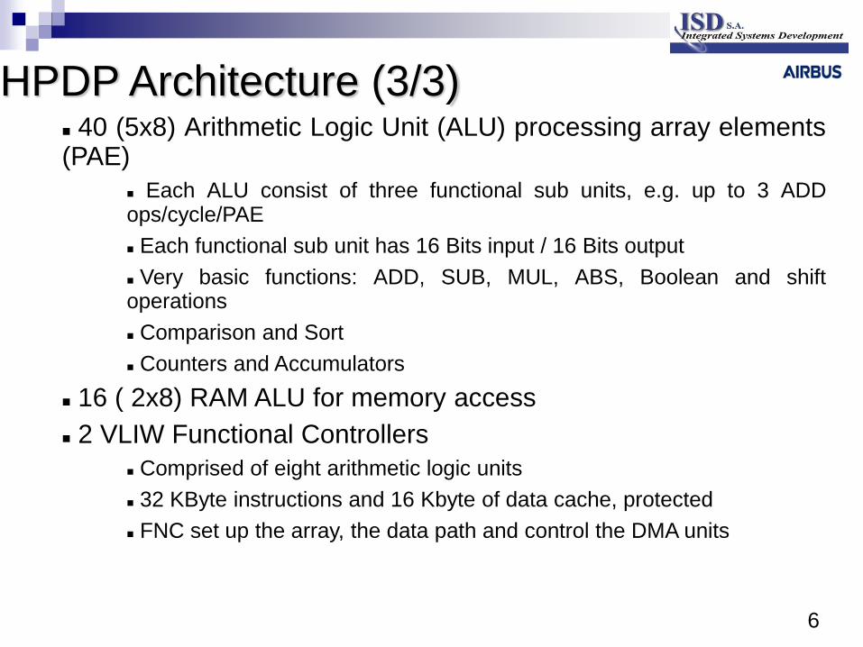
40 (5x8) Arithmetic Logic Unit (ALU) processing array elements (PAE)
Each ALU consist of three functional sub units, e.g. up to 3 ADD ops/cycle/PAE
Each functional sub unit has 16 Bits input / 16 Bits output
Very basic functions: ADD, SUB, MUL, ABS, Boolean and shift operations
Comparison and Sort
Counters and Accumulators
16 ( 2x8) RAM ALU for memory access
2 VLIW Functional Controllers
Comprised of eight arithmetic logic units
32 KByte instructions and 16 Kbyte of data cache, protected
FNC set up the array, the data path and control the DMA units
HPDP Architecture (3/3)
7
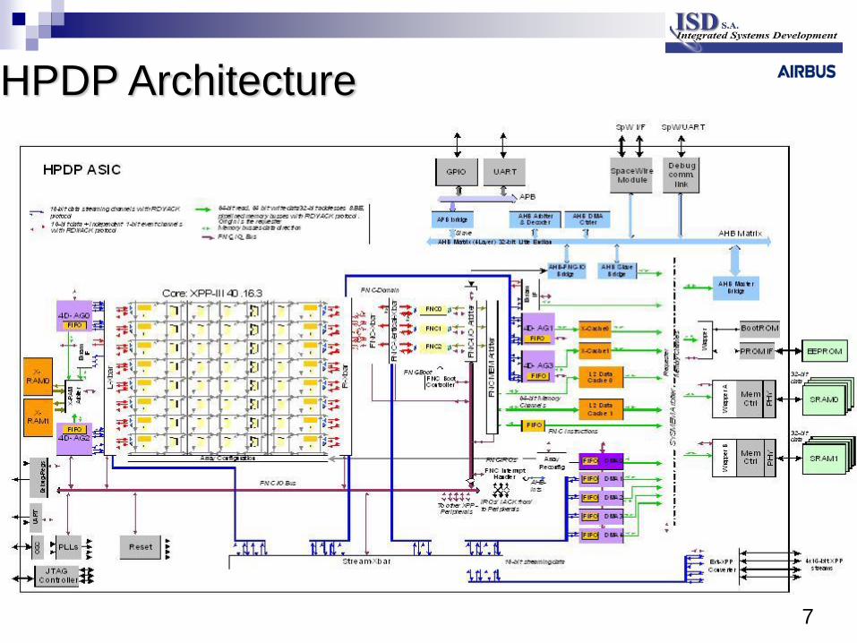
HPDP Architecture
8
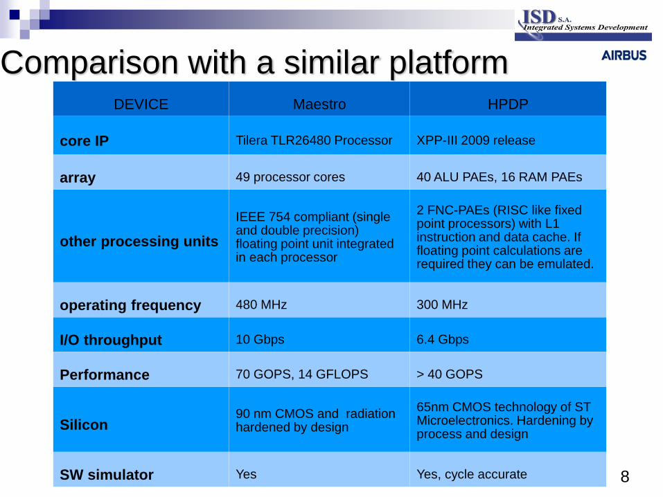
Comparison with a similar platform DEVICE Maestro HPDP
core IP Tilera TLR26480 Processor XPP-III 2009 release
array 49 processor cores 40 ALU PAEs, 16 RAM PAEs
other processing units
IEEE 754 compliant (single and double precision) floating point unit integrated in each processor
2 FNC-PAEs (RISC like fixed point processors) with L1 instruction and data cache. If floating point calculations are required they can be emulated.
operating frequency 480 MHz 300 MHz
I/O throughput 10 Gbps 6.4 Gbps
Performance 70 GOPS, 14 GFLOPS > 40 GOPS
Silicon 90 nm CMOS and radiation hardened by design
65nm CMOS technology of ST Microelectronics. Hardening by process and design
SW simulator Yes Yes, cycle accurate
9
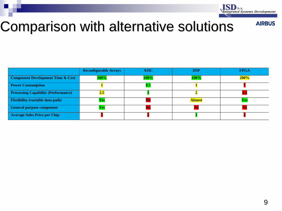
Comparison with alternative solutions
Reconfigurable Arrays ASIC DSP FPGA
Component Development Time & Cost 100% 100% 100% 200%
Power Consumption 1 0.5 1 5
Processing Capability (Performance) 2.5 3 2 0.2
Flexibility (variable data path) Yes No Almost Yes
General purpose component Yes No No No
Average Sales Price per Chip 3 3 1 2
10
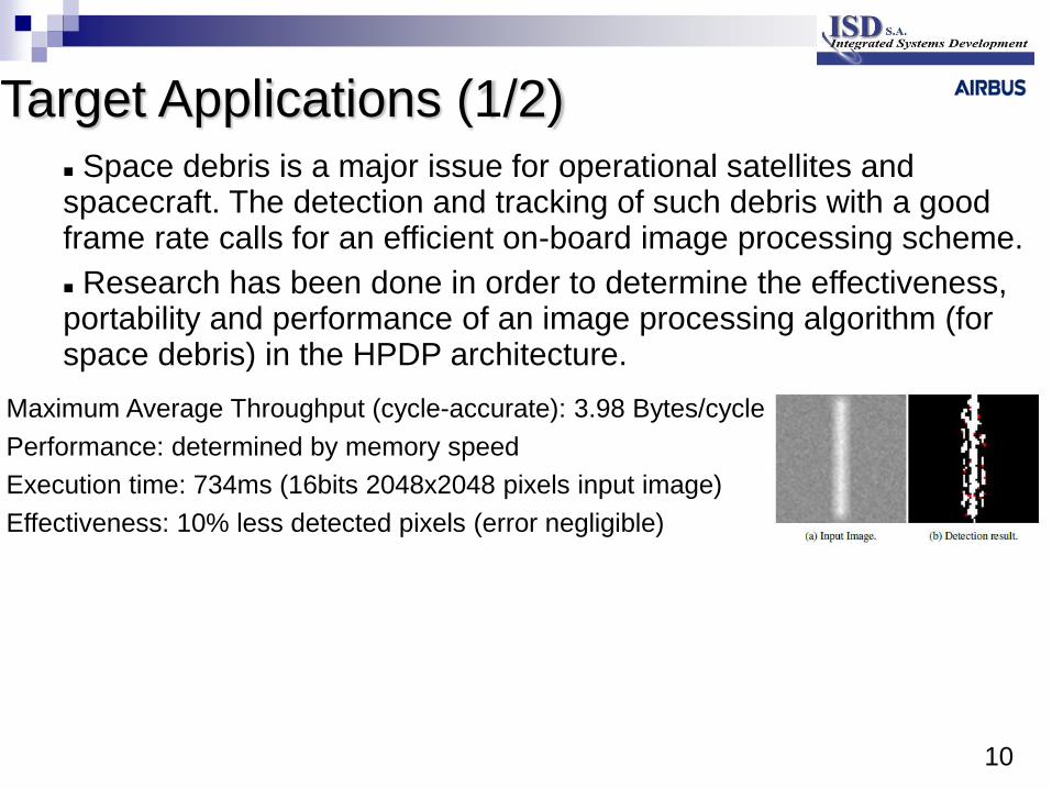
Space debris is a major issue for operational satellites and spacecraft. The detection and tracking of such debris with a good frame rate calls for an efficient on-board image processing scheme.
Research has been done in order to determine the effectiveness, portability and performance of an image processing algorithm (for space debris) in the HPDP architecture.
Target Applications (1/2)
Maximum Average Throughput (cycle-accurate): 3.98 Bytes/cycle
Performance: determined by memory speed
Execution time: 734ms (16bits 2048x2048 pixels input image)
Effectiveness: 10% less detected pixels (error negligible)
11
Telecom
DVB-S Transmitter
DVB-S2 Transmitter
DVB-S Receiver
DVB-RCS Receiver
In-band TC in Telecom satellites
Demodulation in intra-satellite optical communications
etc
Target Applications (2/2)
12
Temperature -55 °C to +125 °C
TID Tolerance >100 kRad
SEL up to 60Mev/mg/cm2 at 125°C
Lifetime in Orbit 20 Years
Operating environment
13
No Hardening at RTL level
Full-custom hardened pad ring
Synthesis with worst case Skyrob cells
Use of hardened clock buffers during clock tree synthesis
Hardened PLLs
Hardened Memory cuts
Deep n-well mask all over except underneath
The pad ring
The memory cuts
The PLLs
Design Flow : On the Hardening
14
Design Compiler version L-2016.03-SP2
Modifications for using hardened memory instances
Synthesis was performed with Skyrob for:
Worst case process
Worst case voltage (1.10V)
Worst case temperature (125C)
20years degradation
Timing and Area constraints were applied (no multi-scenario)
DFT insertion: scan chain insertion to be used in scan mode
Post DFT process: scan enable nets ideal, fix any violated constraint and remove debug interface
Design Flow : Synthesis and DFT Insertion
15
It is performed in order to ensure the correctness of the generated design (compare source code with the synthesized netlist).
Pad Instances and DesignWare Multipliers are handled as black boxes
The overall process is considered as PASSED (the only failing points are the pins of debug interface, that have been removed during post DFT step).
Design Flow : Formal Equivalence Check
16
All the constraints of the design have been integrated in SDC files, manually written, one for each of the modes:
func_pll: main functional mode
func_bypass: functional backup mode, when PLLs are bypassed by primary IO
func_debug_shift: most of the registers in design are connected in one very long shift-register to allow failure debugging by software
scan_stuckat_capture: stuck-at capture mode
scan_stuckat_shift: scan shift mode
scan_tdf_capture: TDF capture mode
They are used:
In preCTS static timing analysis
For the next steps: Place&Route, postCTS static timing analysis (in Primetime type file format)
Design Flow : SDC Files
17
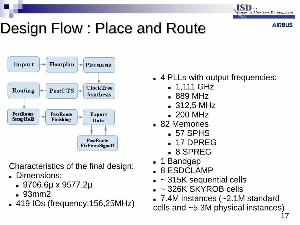
Design Flow : Place and Route
4 PLLs with output frequencies:
1,111 GHz 889 MHz 312,5 MHz 200 MHz
82 Memories 57 SPHS 17 DPREG 8 SPREG
1 Bandgap 8 ESDCLAMP ~ 315K sequential cells ~ 326K SKYROB cells 7.4M instances (~2.1M standard cells and ~5.3M physical instances)
Characteristics of the final design: Dimensions:
9706.6μ x 9577.2μ 93mm2
419 IOs (frequency:156,25MHz)
18
Power Mesh: verified with static IR drop checks.
Pad Ring: full custom development targeting double row classical wire bond. Special attention has been given to optimize ESD protections and anticipate as much as possible the space qualification of the bonding once packaged.
Physical sign-off checks applied during the Place and Route process and on the final design:
successful Gate2Gate Formal Proof
LVS (layout versus schematic) error free
DRC antenna and CrossTalk checks error free
DRC (design rule check) error free with certain justified rules waived.
Design Flow : Place and Route
19
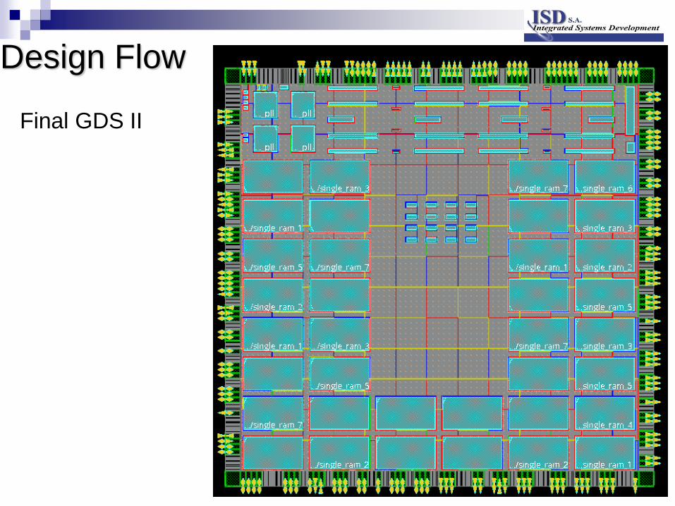
Final GDS II
Design Flow
20
Design Flow : ATPG Automatic Test Pattern Generation
This step concerns the electronic design automation method used to find an input sequence that, when applied to the design, it enables automatic test to distinguish the correct circuit behavior and the faulty circuit behavior due to defects.
The produced patterns are used for testing after manufacturing and at wafer and package level or for failure analysis.
The coverage is almost 96%
Concerning HPDP design, ATPG process was run in two cases:
TDF ATPG
Stuck-at ATPG
The order is selected so as to reduce the amount of test vectors (TDF pattern also check some stuck-at faults).
21
Design Flow : Static Timing Analysis STA is the most important step in the design flow of HPDP, because of its
strict timing requirements.
PreCTS: synthesized netlist and SDC files are used
PostCTS: post layout/routed netlist, SDC files and SPEF file are used
48 different scenarios are checked, 8 cases for each mode:
best case, 1.30V, -40C, RCMIN
best case, 1.30V, -40C, RCMAX
best case, 1.30V, 125C, RCMIN
best case, 1.30V, 125C, RCMAX
Checks done:
successful max transition and max capacitance (with some justified waivers)
successful setup and hold check, by including CRPR update.
correct max clock transition
correct min pulse width check
worst case, 1.10V, -40C, RCMIN
worst case, 1.10V, -40C, RCMAX
worst case, 1.10V, 125C, RCMIN
worst case, 1.10V, 125C, RCMAX
22
Design Flow : Post Layout Simulations
For the moment, the following tests have been run:
AHB_DEF_SLAVE1 Description: the specific test concerns the SpW interface and the basic functionality of the design Status: the test is completed successfully
FFT Description: the specific test concerns the FFT computation Status: FNC starts up correctly and the array is well configured via DMA. Then, it takes time …
23
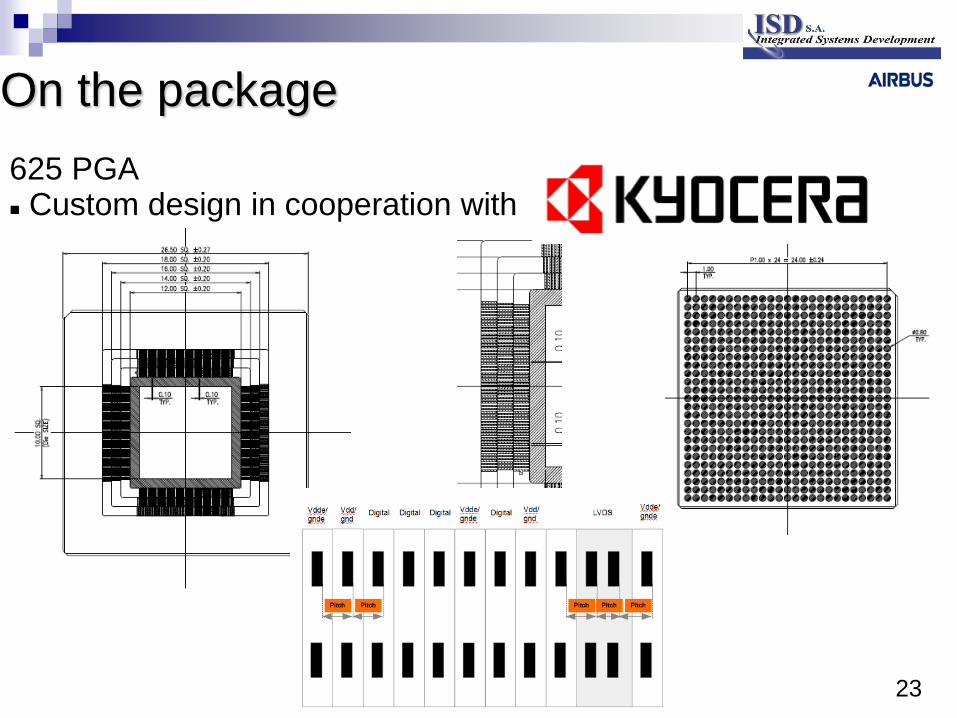
On the package
625 PGA Custom design in cooperation with
24
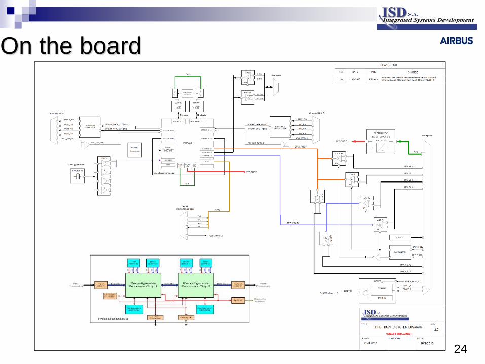
On the board
25
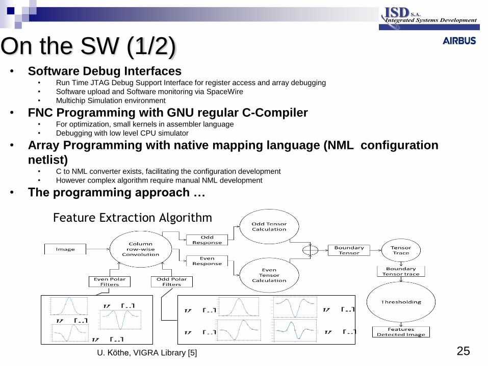
On the SW (1/2) • Software Debug Interfaces
• Run Time JTAG Debug Support Interface for register access and array debugging
• Software upload and Software monitoring via SpaceWire
• Multichip Simulation environment
• FNC Programming with GNU regular C-Compiler • For optimization, small kernels in assembler language
• Debugging with low level CPU simulator
• Array Programming with native mapping language (NML configuration
netlist) • C to NML converter exists, facilitating the configuration development
• However complex algorithm require manual NML development
• The programming approach …
Feature Extraction Algorithm
-5 -4 -3 -2 -1 0 1 2 3 4 50
0.05
0.1
0.15
0.2
0.25
0.3
0.35
0.4
-5 -4 -3 -2 -1 0 1 2 3 4 5-0.25
-0.2
-0.15
-0.1
-0.05
0
0.05
0.1
0.15
0.2
0.25
-5 -4 -3 -2 -1 0 1 2 3 4 5-0.4
-0.3
-0.2
-0.1
0
0.1
0.2
-5 -4 -3 -2 -1 0 1 2 3 4 50
0.05
0.1
0.15
0.2
0.25
0.3
0.35
0.4
-5 -4 -3 -2 -1 0 1 2 3 4 5-0.25
-0.2
-0.15
-0.1
-0.05
0
0.05
0.1
0.15
0.2
0.25
-5 -4 -3 -2 -1 0 1 2 3 4 5-0.2
-0.15
-0.1
-0.05
0
0.05
0.1
-5 0 5-0.4
-0.3
-0.2
-0.1
0
0.1
0.2
0.3
0.4
U. Köthe, VIGRA Library [5]
26
On the SW (2/2) • Reed Solomon Encoder according to DVB-S spec, RS(204,188,T=8)
• Input: Stream of 188 byte frames
• Output: Stream of 204 byte frames
• Reed Solomon Decoder according to DVB-S spec, RS(204,188,T=8) • Input: Stream of 204 byte frames
• Output: Stream of 188 byte frames
• Also outputs number of correctable errors
• Flags uncorrectable packets in TS header
• Convolutional Encoder according to DVB-S spec (G1=171oct, G2=133oct) • Selectable FEC 1/2, 2/3, ¾, 5/6, 7/8
• Viterbi Decoder according to DVB-S spec • Traceback depth configurable (now 512, depends on internal RAM)
• Input: De-punctured soft decision IQ-values (8+8bit)
• Output: Stream of data (2 Byte packed)
• QPSK Modulator according to DVB-S spec • 2/4 times oversampling
• IQ or real output
• Max. 36 tap filter at 4x-oversampling
• QPSK Demodulator according to DVB-RCS Spec • Carrier recovery: Costas-loop with variable parameters
• Timing recovery: Muller&Mueller-loop with variable parameters
• Intersymbol-interference correction by lookuptable
• Input: 2-4 oversampled IQ values
• Output: IQ symbols (8+8bit)
• 32 Point FFT • Input: 32 complex ordered values (8+8bit)
• Output: 32 complex values (8+8bit)
• Internal twiddle factor table
• 16 tap WOLA filter • Weighted overlap filter with variable coefficients
• Input: Stream of complex values (8+8)
• Output: Stream of complex values (8+8)
27
Conclusion
The HPDP project is a complex design, with many considerations taken into account.
After a highly iterative process, the GDS II has been generated and the device has been released for manufacturing, considering that all the possible risks have been minimized.
Applications: HPDP could be used for image processing algorithms (e.g. detecting space debris, telecom), with effectiveness, portability and performance benefits.
28
Acknowlegements
• L. Hili from ESA for his continuous support
• R. Weigand from ESA for his encouragement and support
• T. Scholastique and F. Martin from ST for their precious contribution especially during the back-end phase
• U. Zurek and M. Porcher from Atmel (Microchip) for their support

29
Thank you for your attention!