on site hotbox calibration system project #2
TRANSCRIPT

UNIVERSITY OF ILLINOIS AT URBANA-CHAMPAIGN
On Site Hotbox Calibration
System
Project #2 ECE445 - Design Review
Pourya Assem – Paul Lupas
Prof. Andrew Carl Singer
TA Rajarshi Roy
10/5/2012

Page 1 of 34
Contents Introduction ................................................................................................................................................... 3
Title ........................................................................................................................................................... 3
Problem Statement ................................................................................................................................... 3
Objectives ................................................................................................................................................. 5
Goals ..................................................................................................................................................... 5
Functions ............................................................................................................................................... 5
Benefits ................................................................................................................................................. 5
Features ................................................................................................................................................. 5
Design ........................................................................................................................................................... 6
Block Diagram .......................................................................................................................................... 6
Block Description (More Details Provided in Requirements’ Section) .................................................... 6
TX – Unit .............................................................................................................................................. 7
Transducers Analog Signal Processing ................................................................................................. 7
IR Sensors Analog Signal Processing ................................................................................................... 12
RX – Unit ............................................................................................................................................ 14
Power Supply ...................................................................................................................................... 16
Wheel Calculations ................................................................................................................................. 17
Requirements/Verification ......................................................................................................................... 18
Choke + Fuse ...................................................................................................................................... 18
Amplifier + Clipper ............................................................................................................................. 19
TTL Buffer .......................................................................................................................................... 20
Gain Controlled Amplifier + Active Filter ......................................................................................... 21
TX Microprocessor ............................................................................................................................. 23
XBEE TX/RX Side ............................................................................................................................. 24
RX Microprocessor ............................................................................................................................. 25
SD Card ............................................................................................................................................... 26
GLCD .................................................................................................................................................. 27
Keypad ................................................................................................................................................ 29
TX/RX Power Supply ......................................................................................................................... 29
Tolerance Analysis .................................................................................................................................. 30
Choke .................................................................................................................................................. 30

Page 2 of 34
GC Amplifier for the Heat Sensor ........................................................................................................ 30
Data Acquisition Processor ................................................................................................................. 30
GLCD .................................................................................................................................................... 30
Cost and Schedule ....................................................................................................................................... 31
Cost Analysis .......................................................................................................................................... 31
Labor ................................................................................................................................................... 31
Parts..................................................................................................................................................... 31
Grand Total ......................................................................................................................................... 32
Schedule .................................................................................................................................................. 32
Ethical Issues ............................................................................................................................................... 33
References .................................................................................................................................................. 34
Page 3 of 34
Introduction
Title
The project was selected because of a high demand and immediate need for railroad
companies to be more efficient and accurate in calibrating IR heat sensors, a critical task for
inspecting the train wheels and bearings, enforced by Federal Laws. We are excited to make a
significant improvement in the calibration procedure. We are convinced that this product will be
very marketable because it is a necessary piece of equipment, which has not been implemented
before for railroad companies. Furthermore, the railroad company that we are in contact with has
showed a high interest to buy this device upon completion with rated specifications.
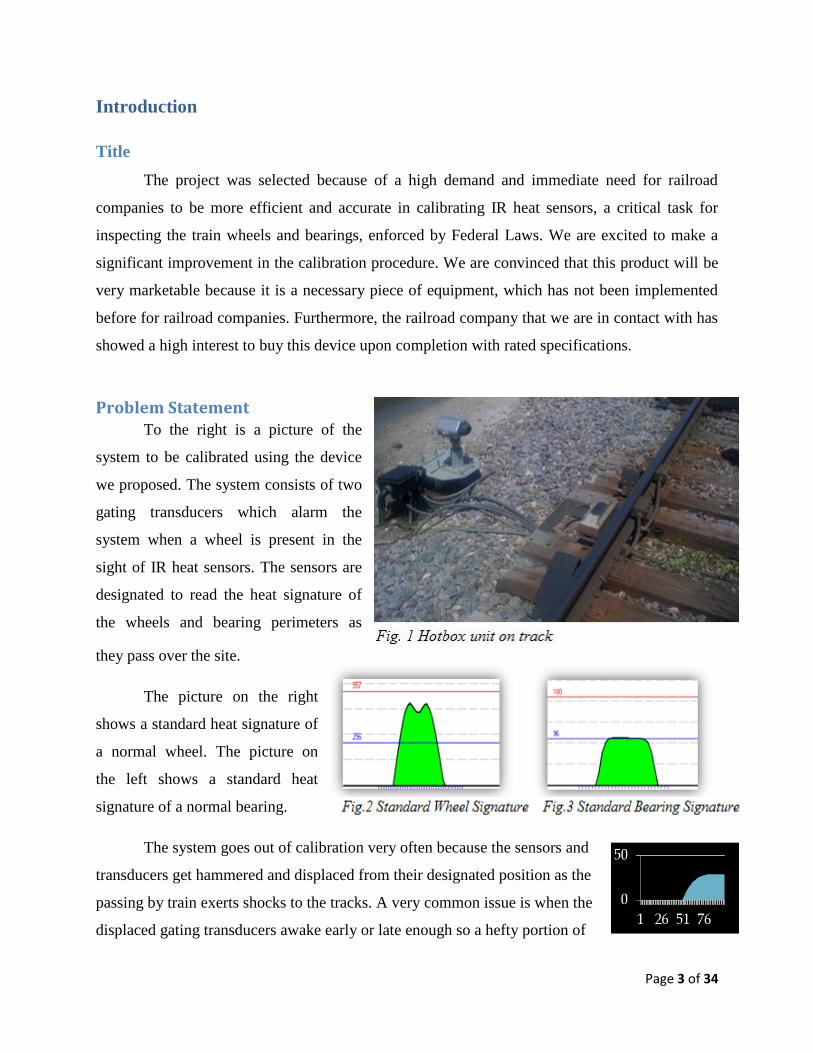
Problem Statement To the right is a picture of the
system to be calibrated using the device
we proposed. The system consists of two
gating transducers which alarm the
system when a wheel is present in the
sight of IR heat sensors. The sensors are
designated to read the heat signature of
the wheels and bearing perimeters as
they pass over the site.
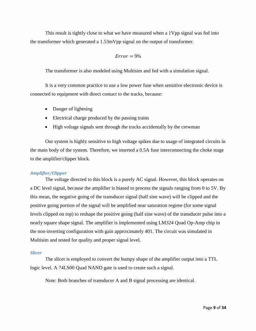
The picture on the right
shows a standard heat signature of
a normal wheel. The picture on
the left shows a standard heat
signature of a normal bearing.
The system goes out of calibration very often because the sensors and
transducers get hammered and displaced from their designated position as the
passing by train exerts shocks to the tracks. A very common issue is when the
displaced gating transducers awake early or late enough so a hefty portion of

Page 4 of 34
heat signature is not recorded by the heat sensors. An example of such behavior is shown above
for late gating. There are other common calibration issues which are not detectable without
observing the heat signatures. A number of such issues are addressed below:
The heat sensors have internal faults
The housing connections are loose which cause abruptions in the transmission of heat
signatures
The heat sensors are shifted and looking at the wrong sight
The sensors are looking into sun
These issues are shown below
The current technology used in the field does not have the ability to fetch and generate
such plots which could allow the service man to detect the issues mentioned above.
0
50
100
1 26 51 76
0
50
100
1 26 51 76
0
200
1 26 51 76
0
100
1 26 51 76
0
100
1 26 51 76
0
100
1 26 51 76

Page 5 of 34
Objectives
Goals
Shift the railroad industry from all mechanical to all electrical sensor calibration devices
Guide servicemen through the calibration process by visualizing the heat signatures
Faster and more accurate calibration process compared to the current mechanical
methods
Create a universal standard for integrating the calibration process
Functions
Acquire data from gate opening and closing transducers
Acquire data from the IR heat sensors
Ensure proper timing synchronization between transducers and IR heat sensors
Ensure proper signal level of transducers and IR heat sensors
Ensure proper wave form read by the IR heat sensors.
Benefits
Service time efficiency due to on-site data analysis and fast feedback
Service cost efficiency due to time efficient method and higher calibration quality
Less data traffic on servers because servicemen do not need to collect data from the
servers
Relatively cheap device ~$50, compared to mechanical calibration tool kit
Wireless data transmission allows service man to keep a safe distance from traveling train
Wireless data transmission allows the service man to collect data in critical weather
conditions and unreachable bungalow locations
Features
Wireless data transmission
SD card data storage
Graphical interface
Battery powered
Small handheld unit

Page 6 of 34
Design
Block Diagram
TX – Unit RX – Unit
Microprocessor Unit
Analog Processing
Analog Processing
Analog Processing
Transducer A Transducer B
IR SensorMixing
Power Supply
XBEE TX
XBEE RX
Microprocessor Unit SD CardKeypad
GLCDPower Supply
Block Description (More Details Provided in Requirements’ Section)
The system consists of two main modules: the TX and RX Module. They communicate
wirelessly through the Zigbee protocol (2.4GHz). This protocol provides fast data transfer,
reliability, and data security. All the other blocks within the TX Module and RX Module are
interconnected using wired connections.
The power supply on the TX side is
connected to the power pins of the analog
processing chips, microprocessor, and XBEE.
The power supply on the RX side is
connected to the power pins of the XBEE,
microprocessor, GLCD and SD Card.

Page 7 of 34
TX – Unit
Transducer A and B
These two blocks are identical and are not part of the system
being deigned. However, our system will connect to them through the
chokes to read the signal. These transducer blocks are responsible for
generating a signal which indicates the presence of the train wheel on
top of the IR heat sensors. The transducer sends a short analog pulse
(one sine period) when a wheel passes over them. In addition, these
pulses activate a shutter covering the IR sensors windows. Above is
an example of how a transducer signal looks like as the wheel passes by.
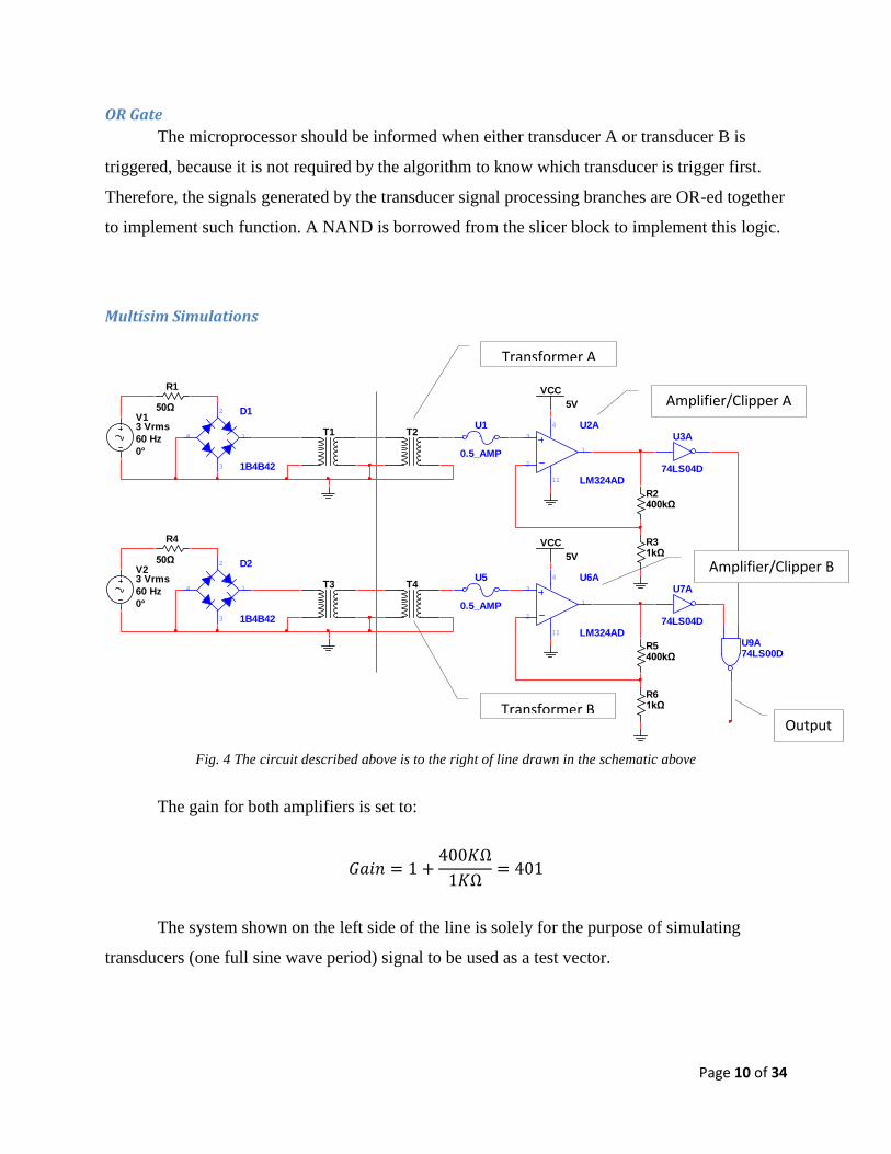
Transducers Analog Signal Processing
Transducer A Chocke/FuseAmplifier/
ClipperSlicer
Transducer B Chocke/FuseAmplifier/
ClipperSlicer
OR Microprocessor
The purpose of this block is to convert the transducer signals into an acceptable
waveform as seen by the microprocessor. The transducer signals will be passed through a 1:1
twisted wire toroidal transformer to meet the specification set by the factory which is perfect
electrical isolation by the third party user. Then the signal is passed through an amplifier which
has a dual function of both amplifying the signal and also clipping the unwanted part of the
signal. The next stage consists of a slicer which converts the clipped signal into an ideal digital
logic signal. Both branches of transducers are finally joined together using an OR gate in order to
send a single signal to the processor which indicates a change of state in either transducers.
1 27 53 79

Page 8 of 34
Choke/Fuse
The choke is made on an iron powder core which has a significant response over the operating
frequencies which is calculated in the following section. Materials needed to build the choke:
White iron powder core of radius 1 cm
Two 1 meter long pieces of AWG 20 transformer wires, twisted on each other
This will make approximately 50 turns. The input and output inductance of the transformer can be
calculated as follows:
Plugging in the values, leads to an input and output inductance of approximately 643uH.
Toroid radius to the center line 1 cm
Coil radius 1 cm
Cross sectional area 3.14 cm2
Wire gauge AWG 20 = 0.518mm
Number of turns 50
Permeability of the core at 20Hz Approx. 41000
The toroid was made and tested in the lab. The inductance obtained was 670uH, as
measured by a multimeter. The coupling factor was nearly 1 as tested by connecting the input of
choke to a function generator at 20Hz and 1Vpp and matching the output signal. The choke
behaves as a band-pass filter with center at 790Hz and 3dB cutoffs at 270Hz and 1.3 KHz. The
function generator is modeled as an ideal voltage source with a 50Ω output resistance.
Connecting the transformer to the function generator will make a voltage divider which
approximately is modeled by the following equation at 20Hz:
Note: The choice of 20Hz is explained in the next section.
Page 9 of 34
This result is tightly close to what we have measured when a 1Vpp signal was fed into
the transformer which generated a 1.53mVpp signal on the output of transformer.
9%
The transformer is also modeled using Multisim and fed with a simulation signal.
It is a very common practice to use a low power fuse when sensitive electronic device is
connected to equipment with direct contact to the tracks, because:
Danger of lightning
Electrical charge produced by the passing trains
High voltage signals sent through the tracks accidentally by the crewman
Our system is highly sensitive to high voltage spikes due to usage of integrated circuits in
the main body of the system. Therefore, we inserted a 0.5A fuse interconnecting the choke stage
to the amplifier/clipper block.
Amplifier/Clipper
The voltage directed to this block is a purely AC signal. However, this block operates on
a DC level signal, because the amplifier is biased to process the signals ranging from 0 to 5V. By
this mean, the negative going of the transducer signal (half sine wave) will be clipped and the
positive going portion of the signal will be amplified near saturation regime (for some signal
levels clipped on top) to reshape the positive going (half sine wave) of the transducer pulse into a
nearly square shape signal. The amplifier is implemented using LM324 Quad Op-Amp chip in
the non-inverting configuration with gain approximately 401. The circuit was simulated in
Multisim and tested for quality and proper signal level.
Slicer
The slicer is employed to convert the humpy shape of the amplifier output into a TTL
logic level. A 74LS00 Quad NAND gate is used to create such a signal.
Note: Both branches of transducer A and B signal processing are identical.
Page 10 of 34
OR Gate
The microprocessor should be informed when either transducer A or transducer B is
triggered, because it is not required by the algorithm to know which transducer is trigger first.
Therefore, the signals generated by the transducer signal processing branches are OR-ed together
to implement such function. A NAND is borrowed from the slicer block to implement this logic.
Multisim Simulations
Fig. 4 The circuit described above is to the right of line drawn in the schematic above
The gain for both amplifiers is set to:
The system shown on the left side of the line is solely for the purpose of simulating
transducers (one full sine wave period) signal to be used as a test vector.
V13 Vrms
60 Hz
0°
T1
R1
50Ω D1
1B4B42
1
2
4
3
T2U1
0.5_AMP
U2A
LM324AD
3
2
11
4
1
VCC
5V
R2400kΩ
R31kΩ
U3A
74LS04D
V23 Vrms
60 Hz
0°
T3
R4
50Ω D2
1B4B42
1
2
4
3
T4U5
0.5_AMP
U6A
LM324AD
3
2
11
4
1
VCC
5V
R5400kΩ
R61kΩ
U7A
74LS04D
U9A74LS00D
Transformer A
Transformer B
Amplifier/Clipper A
Amplifier/Clipper B
Output
Page 11 of 34
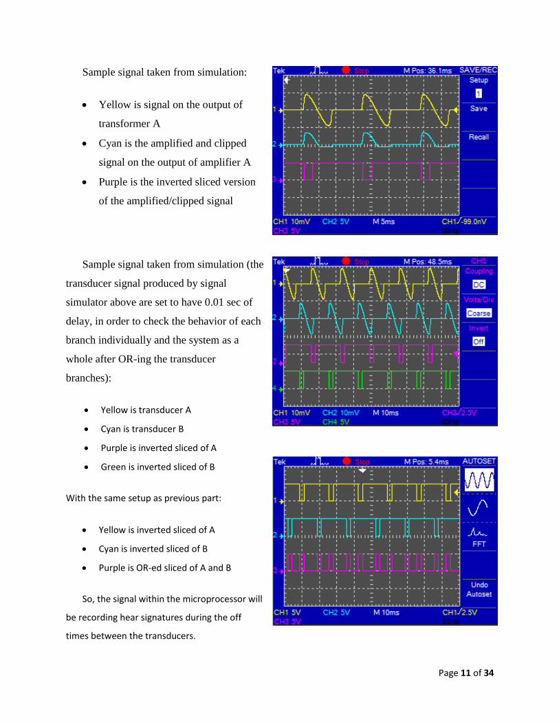
Sample signal taken from simulation:
Yellow is signal on the output of
transformer A
Cyan is the amplified and clipped
signal on the output of amplifier A
Purple is the inverted sliced version
of the amplified/clipped signal
Sample signal taken from simulation (the
transducer signal produced by signal
simulator above are set to have 0.01 sec of
delay, in order to check the behavior of each
branch individually and the system as a
whole after OR-ing the transducer
branches):
Yellow is transducer A
Cyan is transducer B
Purple is inverted sliced of A
Green is inverted sliced of B
With the same setup as previous part:
Yellow is inverted sliced of A
Cyan is inverted sliced of B
Purple is OR-ed sliced of A and B
So, the signal within the microprocessor will
be recording hear signatures during the off
times between the transducers.

Page 12 of 34
IR Sensors Analog Signal Processing
An active filter was used to filter and amplify the signal coming from the IR heat sensors.
The gain of amplifier should be adjustable in order to provide an appropriate range to the ADC
of the microprocessor which ranges from 0 to 5V. The filter is a 2nd
type low pass configuration
with cutoff frequency at 1 KHz, providing 40dB of attenuation. The active part was implemented
utilizing a non-inverting Op-Amp borrowed from the LM324 (used in the transducers branch).
The cutoff frequency and gain can be calculated as follows:
=
√
Fig. 5 The circuit to the right of the line drawn above is the active filter
The series of AC source signals to the left of the line drawn above was implemented to
approximately simulate the bearing heat signature read by the IR sensors, plus a 2 KHz
sinusoidal signal to test the filter.
Note: The heat signature circuit does not include a choke and fuse, because it is
implemented within the breakout circuit inside the heat scanners. In addition, R10 and R11 can be
replaced by a pot to adjust the gain.
R7
50Ω
U4A
LM324AD
3
2
11
4
1
VCC
5V
R8
16kΩ
R9
16kΩC110nF
C2
10nF
R100Ω
R111kΩ
V31 Vpk
40 Hz
0°
V40.3 Vpk
80 Hz
0°
V52 Vpk
2kHz
0°
Output

Page 13 of 34
Simulations
The sample signal taken from active
filter simulation:
Yellow is the approximated bearing
signature for 8 axles back to back (no
inter-trucks)
Cyan is yellow plus 2 KHz sinusoidal
injected into the amplifier
Purple is the filtered output
Data Acquisition Processor
This is the decision making block of
the system for the TX Unit. The
ATMEL328 chip is programmed to
implement all the functions of this block.
The chip has a 10bit ADC which will take
as input the amplified IR heat sensor signal.
The processor reads a digital signal from
OR-ed transducer signal and the IR sensor.
It will combine these signals into a single
array to have the following sequence:
transducer signal, heat signal, transducer
signal. This sequence includes the data for
one wheel. The serial output of the
processor will send this data array to the
TX Xbee block.
Check for signal from Transducer, if first
transducer
NO
Reset time counter
Check for signal from transducer, if second transducer and check timer for being less
Transducers OR-ed data
YES
YES
ADC Data
Send to Data + transducers to XBEE
XBEE
More than 10 min, reset the system
NOStop, reset the
system

Page 14 of 34
TX XBEE
This block is implemented using a XBEE wireless
module. It is responsible for transmitting the serial data
generated by the processor block from the TX Unit. The
XBEE wireless module employs the Zigbee protocol to
communicate to the receiver module.
RX – Unit
RX XBEE
This block is implemented using XBEE wireless module. It is responsible for receiving
the serial data from the TX Xbee. The connections will be similar to what was described in the
TX Xbee.
Main Processor
This block uses the ATMEL328
chip to analyze the data received by the
RX block. It has an algorithm that
searches for the transducer pulses. As
soon as a transducer pulse is observed,
a counter is triggered which interrupts
data analysis if the time between
transducer pulses is greater than 3
seconds. Another algorithm works in
parallel to check for data between the
transducer pulses and send it to the
memory block. If the time between the
two transducer signals is greater than 3
seconds, the user gets the permission to
access the data from the SD card. The 3
second time interval is calculated for a
Send data to SD card
Close the text file
Open the file to be read
first transducer present
RX XBEE
NO
Check transducer
YES
YES
Send # to SD card
Reset timer
More than 3 seconds
YES
User request data
YES
YesRead # and send
dataHold data 0.5 sec in
buffer
Send to GLCDIf end of fileClose file
Page 15 of 34
train traveling at 20mph. So, if the time interval is greater than 3 seconds, it means that the train
passed over the site and all the wheels/bearings are scanned.
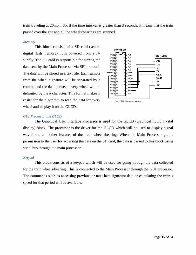
Memory
This block consists of a SD card (secure
digital flash memory). It is powered from a 5V
supply. The SD card is responsible for storing the
data sent by the Main Processor via SPI protocol.
The data will be stored in a text file. Each sample
from the wheel signature will be separated by a
comma and the data between every wheel will be
delimited by the # character. This format makes it
easier for the algorithm to read the data for every
wheel and display it on the GLCD.
GUI Processor and GLCD
The Graphical User Interface Processor is used for the GLCD (graphical liquid crystal
display) block. The processor is the driver for the GLCD which will be used to display signal
waveforms and other features of the train wheels/bearing. When the Main Processor grants
permission to the user for accessing the data on the SD card, the data is passed to this block using
serial bus through the main processor.
Keypad
This block consists of a keypad which will be used for going through the data collected
for the train wheels/bearing. This is connected to the Main Processor through the GUI processor.
The commands such as accessing previous or next heat signature data or calculating the train’s
speed for that period will be available.

Page 16 of 34
Power Supply
Both TX and RX units are powered by a 5V supply. This voltage is regulated by the
circuit shown above. This circuit is capable of delivering 5VDC @ maximum drive current of
1Amp. The input voltage can be chosen from a range of 7V to 32V, which is suitable for running
the system by a 9V battery. The power consumed by the TX and RX units is calculated below:
TX unit at sleep mode5mA (Xbee) + 5mA(processor) + 10mA(all three
amplifiers) + 2mA(TTL chip) = 22mA @ 5VDC = 110mW
TX unit at active mode35mA(Xbee) + 10mA(processor) + 30mA(all three
amplifier) + 2mA(TTL chip) = 77mA @ 5VDC = 385mW
RX unit at active mode35mA(Xbee) + 10mA(processor) + 2mA(SD card) +
15mA(GLCD) = 62mA @ 5VDC = 310mW
According to the above specifications, the voltage regulator is capable of handling such
power requirements. The TX unit running on a standard 1000mAh battery will last for less than 8
hours (in sleep mode) and 3 hours in active mode. The RX unit can be operated on the battery for
less than 3 hours. The alternative option for providing TX unit with the rated power is a solar
panel.

Page 17 of 34
Wheel Calculations
Car Car
920" 30" 120"48"
Inter-Truck Inter-CarInter-WheelWheel Diameter
The picture above shows the extreme dimensions of a standard train car operated in
Northern America. There are five major sizes that characterize the metrics used in designing the
system.
Inter-Truck Distance 920 inches
Inter-Car Distance 120 inches
Inter-Wheel Distance 30 inches
Wheel Diameter 48 inches
Closing-Opening Transducer Spacing 50 inches
The transducers will trigger when the center of the wheel is aligned with the center of
transducers. The calculations below are carried out to find the shortest timespan between the
triggering pulses coming from the transducers. The timespan is a function of the train’ speed and
the spacing addressed above. The two speed extremes are 20 mph for the lower and 60 mph for
the upper bound.
The shortest time is calculated for the train going at the fastest speed, when a wheel
passes a closing transducer and the next wheel passes the opening transducer. This distance is the
axle to axle spacing of the two closest wheels minus the transducers spacing, which is
24+30+24-50 = 28 inches. The top speed is 60mph = 1056 in/sec, which means the minimum
transducer timing is 26.5ms.
The longest time is calculated for the train going at the slowest speed, when the two
furthest (truck to truck) wheel pass over the transducers. The longest distance is 24+ 920+24 =
968 inches. The train’s slowest speed at 20mph = 352 in/sec. This results in 2.8sec.
As calculated, the minimum time was 26.5ms. The algorithm developed in the TX Unit
should be fast enough to distinguish transducer pulses 26.5ms apart from each other. The

Page 18 of 34
microprocessor used in the TX Unit is capable of processing or reading digital pulses as short as
a tenth of a millisecond.
The transducer spacing is set to 50 inches, which results in wheel scan time of 47ms for
the train going at 60 mph. A minimum number of 12 samples are needed for each wheel scan,
which requires minimum read time of 4ms for each sample. The ADC should be fast enough to
handle such conversion rate. The microprocessor ADC has conversion rate of 10 kilo samples
per second which satisfies the requirement.
Requirements/Verification
Choke + Fuse
Requirement Verification
a). Chokes should not drain more than
allowable current as specified by the
manufacturer (GE). The maximum rated drain
power is 400mW.
b). The chokes have to have a linearly
increasing response over frequency span of
10Hz to 500Hz with 1:1 transfer ratio, and
minimum coupling loss.
c). The chokes have to have small
impedance over the operating frequency range
of 10Hz to 500Hz.
d). The fuse should be capable of
handling 0.5A. Fuses are for the mere reason of
preventing high voltage spikes entering the
calibration system. This is a common practice
in railroad equipment, because of lightings and
static charge dangers.
1. Wrap the twisted wire
transformer (choke) as
specified by the
calculations. Make sure
each leg of the twisted pair is of the
same size, 1 meter. There should be
exactly 50 turns on each transformer
and make sure the wires are tightly
wrapped on the core with a minimum
of 30 degrees spacing between the
terminals.
2. Connect the input of the transformer to
a function generator @ 5Vpp - 10Hz
sinusoid and trace the output with the
resolution set on averaging. This signal
should be @ 3.83mVpp – 10Hz
sinusoid with maximum phase shift of
6 degrees w.r.t function generator. 3. Set the 2
nd channel of the oscilloscope
to trace the input signal of the
transformer. This signal should be @
3.83mVpp – 10Hz sinusoid. Use the
Math function to subtract the input and
output signals to ensure a perfect
match. This indicates a high coupling
factor. 4. Increase the function generator
frequency to 20Hz and repeat step 3
(this time @ 7.65mVpp) to check for

Page 19 of 34
coupling factor.
5. Repeat step 3 for frequencies up to
500Hz. 6. If the coupling factor differs or decays
over the frequency span, repeat step 1
with a core (better low frequency
handling characteristics) and ensure the
twisted wires are tightly wrapped. 7. Use two DMMs to monitor the current
and voltage on the input of transformer
and find their product to ensure the
drain power is below 400mW.
8. If the specs on step 7 are not met,
increase the number of turns and repeat
steps 1-7 (iteratively and calculate new
voltage values on the output using the
equations provided). 9. If the above steps are satisfied, make a
second transformer. 10. For more accurate measurements, use a
Network Analyzer to check for all the
specs. 11. Connect the fuse to the output of the
transformer and trace the output @
10Hz and 20Hz to ensure the values
match with the voltages provided in
steps 3 and 4. If not, change the fuse
and repeat step 11.
Amplifier + Clipper
Requirement Verification
a). This stage is directly fed from fuses,
with minimum power consumption.
b). The expected input from transducers
at the fastest rate is a one full sine wave period
every 26.5ms and 3s for the slowest rate.
c). The pulse period is positively
correlated to the time span between the pulses.
We expect to see a quiet time or low noise
level between the pulses at the output.
d). The amplifier circuits should be
tuned to provide a large enough pulse to drive
the TTL buffer.
e). Amplifier gain is expected to be
within a controllable range of 200 to 401.
1. Construct the amplifier as shown in
Fig.4 and use a DMM to monitor the
current being drained by the Quad
Amplifier Chip (LM324).
2. Set the potentiometer to obtain a gain
of 200 and check the input/output
response as described in the next step.
3. Set the function generator @ 20mVpp -
10Hz sinusoid. Amplify the signal
using the amplifier built and tuned in
step 1-2 and trace the output on the
oscilloscope to have the right frequency
and non-inverted amplitude of 2Vpp -
clipped with maximum phase shift of 6

Page 20 of 34
degrees.
4. Repeat step 3 with 20Hz (amplifier
output @ 4Vpp - clipped).
5. Change the gain to 401 and repeat steps
3 and 4, and check for output voltages
of 4.01Vpp and approximately 4.70Vpp
correspondingly.
6. Note: The amplifier power rails are
biased from 0 to 5VDC, and signal
coming from generator is purely AC.
So the signal will be clipped (rectified)
in steps 4 and 5.
7. If the voltage levels are not within the
mentioned values in step 5, increase the
gain above 401.
8. Consistently, during all these steps,
check for the current drained by the
amplifier to ensure it does not exceed
30mA.
9. Build the second branch of amplifier
for the second choke and repeat steps 1-
8.
10. In steps 1-9, the amplifier is driving a
1KΩ resistor (simulating a TTL Buffer).
11. In steps 1-9, check the output signal of
the amplifiers when no input signal is
injected to the input terminals (tied to
ground). The output signal should have
a minimum noise level. Preferably for
TTL logic safety, the noise level should
be less than 0.3V.
12. If any of the specs are not met, change
the Amplifier Chip is a lower power
noise version. Additionally if the gain
values can be redefined to meet the
specifications.
TTL Buffer
Requirement Verification
a). This stage is fed by the amplifier
stage, to convert the clipped signal to an
acceptable TTL logic level by the
microprocessor’s digital ports. Meanwhile, it
provides a wide noise margin.
b). TTL buffers should be provided
1. Use the Quad NAND gate chip
(74LS00) to implement the
combinational logic as shown in Fig. 4.
2. Use a 1MΩ resistor on the output of the
combinational logic to simulate the
microprocessor digital port impedance.

Page 21 of 34
enough input power for proper operation. The
input signal from the amplifier should not have
a steady state in the unknown region of TTL
operation. The TTL output is directly
connected to the microprocessor providing a
full TTL logic swing.
3. Use a DMM on the power line
connecting to the chip to monitor the
drain current. It should not be more
than 2mA. If it is not the case, replace
the TTL chip with a lower power
version.
4. Connect one of the inputs of the
combinational logic (OR) to a function
generator set at 10Hz square wave (0-
5V swing) and the other input to
ground. Trace the output signal to
ensure full swing and the pulse shape
(perfect square wave) matches the
input.
5. Repeat step 4, this time with 10Hz
square wave at a lower swing (0-4V).
This test should be performed because
the signals coming from the amplifier
stage were calculated to have similar
values for the rated frequency.
6. If step 5 is not passed then reconfigure
the amplifier gain (to a higher value),
so the amplifier output swing is within
the acceptable TTL range.
7. Increase the frequency to 20Hz and
repeat steps 4-6.
8. In all steps, trace the noise level
(tolerance) of the input signal and
ensure it is not more than 0.3Vpp
Gain Controlled Amplifier + Active Filter
Requirement Verification
a). Scale up or down the IR sensors’
signal to an acceptable level seen by the
microprocessor's ADC. The ADC range is 0 to
5VDC with 10 bit resolution.
b). The amplifier should have a low
noise level, low power consumption and
controllable gain of 0.5 to 5.
c). The LP filter should have a 2nd
order
implementation with cutoff at 1KHz. The
response should be as flat as possible over
frequency span of 10Hz-500Hz.
1. Build the active filter as shown in
Fig.5. Connect a 1MΩ resistor as the
load to simulate the microprocessor
ADC.
2. Use a DMM to monitor the current
drain by the amplifier chip. It should be
less than 30mA, while all three (two
from transducers + active filter
amplifier) are loaded and running.
3. Use the function generator to generate a
50Hz sinusoid with 1Vpp and 0.5VDC
bias to simulate the heat signature
signal as read by IR sensor. Make sure

Page 22 of 34
the function generator is set to 50Ω mode to simulate the IR sensor terminal
impedance. Set the amplifier gain to 1
by choosing the feedback resistance to
be 0Ω. This resistance (consequently the
gain) is controlled by a potentiometer
(log tape 0-500KΩ).
4. Read the signal level on the input of
active filter. This signal should not be
less than less than 0.9V. Otherwise, the
feedback loop or the filter’s resistive
network has a bad connection. Double
checks the active filter to ensure the
right components are used.
5. If step 4 is passed, use the function
generator’s sweep mode to sweep the
signal injected into the active filter
from 10Hz to 2KHz. Trace the output
using an oscilloscope to ensure flat
response over the critical region 10Hz
to 500Hz and 80dB attenuation over
1KHz cutoff point. If the signal is not
attenuated by the rated value at 1.2KHz
then shift the cutoff point toward a
lower frequency (not lower than
800Hz). The 800Hz was chosen to
satisfy the bandwidth of heat-signature
signal.
6. Adjust the function generator to
generate a 50Hz sinusoid of 3Vpp (a
common heat-signature peak value)
with 1.5VDC bias. Change the gain
(increase) using the potentiometer and
trace the output signal of the active
filter to bring up the peak voltage level
value to approximately 4.5V. The 5V
ADC limit is not used to provide
headroom for the heat-signature to
prevent clipping in case the input signal
exceeds 3Vpp limit.
7. Inject the signal described in step 6 + a
square wave with fundamental
frequency at 1.5 KHz, and trace the
output signal to ensure the additive
noise (in this case square wave) is well
attenuated.

Page 23 of 34
8. If step 7 is not passed, repeat steps 3-7
to adjust the gain and cutoff frequency
to a reasonable value so that the output
signal has a proper signal level (not
higher than 4.5V) and noise level.
9. Note: For reconfiguring the cutoff
frequency it is easier to change the
active filter resistors’ values (utilizing a
pot eases the tuning process).
TX Microprocessor
Requirement Verification
a). Should be able to handle process and
transmit the collected data into a serial
connection, fast enough for a train at 60MPH.
b). The microprocessor is clocked at
20MHz. So the calculation should be
performed to take enough number of samples
for a train going at minimum and maximum
speed.
c). The sampling at 8KHz should be
downed sampled according to these
calculations, and optimized for minimal data
traffic on the serial data bus going to XBEE
TX at 9600 baud rate.
1. Ensure the connections from TX
microprocessor to TX XBEE are
correct. TX of the microprocessor goes
to the RX of the XBEE and the RX of
the microprocessor goes to the TX of
XBEE.
2. There are several triggering algorithms
running in parallel which are controlled
by a watchdog timer. The watchdog
timer should be reset at the beginning
of each iteration. Failing to do so, will
prevent the algorithm from being reset.
3. The main functioning trigger is the
transducer detection algorithm. If in
case of any malfunction, this algorithm
should be tested individually (in the
first step of troubleshooting procedure)
to evaluate its proper timing and
correlation to incoming transducer
signals. The most important body of
this algorithm is the most frontal stage
responsible to detect the first transducer
followed by the second transducer
within a predefined period (as defined
in the flowchart and calculations). This
stage tells the TX processor to wake up
and start fetching next incoming
transducer pulses along with the heat-
signature. Use a function generator to
feed the transducer’s digital port
reserved on the TX microcontroller.
Change the duty cycle until the low

Page 24 of 34
time of the square wave is less than the
specified time span mentioned in the
calculations and use the serial terminal
to send checkpoints if the algorithm
detected and triggers the wake-up
signal. Decreases the duty cycle until
the low time is larger than the time
span specified in the calculations. Use
checkpoints to be sent to serial terminal
to ensure the algorithm does not trigger
the wake-up signal.
4. The next layer of troubleshooting the
TX microprocessor is to feed the data
acquisition’s trigger manually to ensure
the transducers and sampled heat-
signatures are mixed and saved to an
array properly. Feed the newly created
array (transducers + heat-signatures)
into the serial terminal (to a computer)
and verify if the signals going into the
microprocessor match with data
obtained on the serial terminal.
5. Ensure the serial transmission rate is
fast enough so the data traffic will not
prevent data samples to get lost or
delayed. This can be done by setting
the serial baud rate to values higher
than 9600.
6. If steps 1-5 are passed, connect XBEE
to the TX processor and connect RX
XBEE to the computer. Feed the TX
chip with simulated signals and read
the data transmitted to the computer.
XBEE TX/RX Side
Requirement Verification
a). Make proper connection with the
microprocessor through the serial protocol.
b). The maximum distance between the
TX and RX is 30 meters.
c). The TX and RX should
communicate with each other and the
microprocessors at baud rate of 9600.
1. Connect RS232 serial cable to XBEE
units on two separate computers and
use the terminal port to send and
receive specific test vectors. 2. If the transmitted data matches the
received data, then program two
microcontrollers to send and receive a
known test vector of ASCII characters

Page 25 of 34
over a wired channel. Check for
accuracy of received data (with 0 bit
error rate). 3. Connect the XBEE units to the
programed microcontroller from step 2
and check for accuracy of data received
(ideally 0 bit error rate).
RX Microprocessor
Requirement Verification
a). The XBEE transceiver on the RX Unit
and RX microprocessor communicate with
each other through serial protocol at a baud
rate of 9600.
b). The algorithm has to detect transducers
pulses so that the samples of the heat-signature
is logged on the SD card.
c). The multiplexer is used to switch
between XBEE to the GLCD at proper timing.
1. Ensure the connections from RX XBEE
to the RX microprocessor are correct.
TX of the XBEE goes to the RX of the
microprocessor and the RX of the
XBEE goes to the TX of
microprocessor. Ensure the data
transmission baud rate is set to values
higher than 9600 (to prevent data
traffic, loss of data samples).
2. There are several triggering algorithms
running in parallel which are controlled
by a watchdog timer. The watchdog
timer should be reset at the beginning
of each iteration. Failing to do so, will
prevent the algorithm from being reset.
3. The main functioning trigger is the
transducer detection algorithm. If in
case of any malfunction, this algorithm
should be tested individually (in the
first step of troubleshooting procedure)
to evaluate its proper timing and
correlation to incoming transducer
signals. This algorithm looks for
transducer signals by checking the max
(1023) value from the incoming array
of data (1023 is only reserved for
transducers and heat-signature cannot
have such a high value).
4. The most important body of transducer
detection algorithm is the watchdog
timer that activates the SD Card
interference algorithm. As calculated,
this watchdog timer should cut off the
data link going to the SD Card, if no
transducer is detected within 10 min

Page 26 of 34
period. Test this functionality by
manually feeding signals using the
serial port to the microprocessor and
use checkpoints to evaluate proper
functioning of this watchdog timer.
5. If step 4 is passed, test the algorithm
that isolates the transducer signals from
the array of incoming data and provides
the heat-signature in array form to be
saved individually on the SD card. Test
this algorithm by manually sending a
mix of transducer signals and heat-
signature array through the serial port
from computer to the processor. Use a
checkpoint to verify proper isolation
heat-signature data from the transducer
signal on the serial port connect to the
computer.
6. If step 5 is passed, test the SD card
following the SD card verification
procedure.
7. Ensure the algorithm that cuts off the
data logger algorithm to the SD card
and provides the link for the user to
access the SD card data also triggers
the multiplexer used to switch the serial
port from XBEE interference to the
GLCD at the same time along with
sending reset signal to the GLCD to
refresh its memory, otherwise the
GLCD will not function properly.
SD Card
Requirement Verification
a). It should be compatible with the
driver, either FAT16 or FAT32 file format.
b). The memory size should not exceed
8GB.
c.) Writing to a text file on the SD card
should take 2ms at 9600 baud rate.
d) The data read from text file should
be identical to the data present in the text file.
1. Connect the SD card to an Arduino
microcontroller as shown in Fig. 7.
Upload the ‘card info’ code and ensure
the SD card is in the FAT16 or FAT32
file format. Also ensure that the SD
card does not exceed 8GB. 2. Using the same configuration, upload
the ‘write to file’ code and check that it
takes 2ms at 9600 baud rate using the
serial monitor. Repeat this process 6
times to ensure full functionality.

Page 27 of 34
3. Using the same code as in step 2, write
a predefined array of 20 digits to an
empty text file. Power off the
microcontroller. Take the SD card out
and check with a card reader that the 20
elements of the array were written only
once. Repeat this step 6 times to ensure
full functionality. 4. To check the reading functionality,
upload the ‘read from file’ code and use
the serial monitor to read serially all the
data on the file. Repeat this process 6
times to ensure full functionality.
GLCD
Requirement Verification
a). The GLCD should be capable of
handling baud rate up to 115200 using serial
protocol.
b). Both TX and RX serial terminals
are used to establish a connection between
GLCD and the RX microprocessor. So, the
microprocessor RX and TX terminals are
reserved for GLCD.
c). The firmware installed on GLCD
should support and feature SGC serial
protocol, because the driver has been written
for this protocol (do not use GSX).
1. The GLCD driver is only compatible
with Arduino Compiler 002X.
2. Make sure the TX of the
microprocessor is connected to RX of
GLCD, and the RX of microprocessor
is connected to the TX of GLCD.
3. The datasheet and GLCD drivers can be
downloaded from the manufacturer
website (included in the references
section).
4. Make sure when the initialization
process is done in the microprocessor
the baud rate is set to 115200.
5. Make sure the transparent mode is
activated during initialization otherwise
the GLCD will remain black all the
time.
6. Make sure the RESET of GLCD is
connected only to the RESET of
microprocessor and there are no other
external analogs interfering with the
RESET pin.
7. The alphabetical print command is
passed by reference type and passing
strings by value will not display
anything on the screen.
8. The algorithm that fetches the data
from SD card and responsible for
ASCII to integer conversion is
Page 28 of 34
embedded within the GLCD algorithm.
Any type of conversion (down
sampling) should be performed with
respect to GLCD screen size with
minimum loss of data.
9. The most number of pixels shown on
the horizontal scale is 128 so the data
points for each heat-signature which is
usually in the range of roughly 300-500
should be down sampled by a factor of
2 to 4. The algorithm should calculate
the exact down conversion rate (for
example 2.34 for the case of 300) so the
down sampling conversion is optimized
for minimum data loss.
10. After all the train wheels are scanned
(detected by the microprocessor when a
delay of 3s is seen between the
transducer pulses), the user gets access
to read the SD card and activate the
GLCD algorithm. If GLCD and
interference keys are not locked during
that time, the writing process gets
interrupted and data samples will be
lost. Therefore, check proper triggering
of GLCD algorithm controlled by the
main running algorithm on RX
microprocessor.
11. If the data on the screen has missing
components that could be caused by
static arrays which should be avoided
and instead utilize heap memory.
12. The algorithm structure should allow a
minimum of 5ms for each write
instruction as well as clear and
refreshing signals. So displaying a full
heat signature can take up to 0.6
seconds.
13. Reset the GLCD and microprocessor if
they do not hand shake and random
pixels are displayed on the screen.

Page 29 of 34
Keypad
Requirement Verification
a). The keypad should be a 4x4 matrix
(8 pins for vertical-horizontal scan) type.
b). The keypad should be a resistive
type network, because the library written for
this type of keypads (as opposed to capacitive
network keypads).
1. Set the DMM to continuity mode.
Connect the DMM to all possible
combinations of rows and columns.
Check all the keys for each
combination, and ensure that only the
corresponding key of that row and
column makes a closed circuit. 2. Connect rows and columns of the
keypad to the microprocessor and
upload the test program. Press all the
keys and check the right key is detected
on the serial terminal.
TX/RX Power Supply
Requirement Verification
a). It should provide a regulated 5VDC
at minimum drive current of 400mA.
b). This power supply is being used to
drive all the blocks within the TX and RX
units.
c). The voltage regulators are fed by a
9VDC-32VDC supply capable of handling a
minimum of 410mA (the extra 10mA is saved
for the voltage regulator internal circuitry).
1. Load both voltage regulators by a
proper resistive load (10-12Ω) to ensure
drive current of 400mA.
2. Use the function generator to couple the
input power supply of the voltage
regulators with the 60Hz sinusoid
0.5Vpp. Monitor the regulated signal
on the output. If the voltage variation
on the output of voltage regulator is
more than 0.005Vpp, then change the
bypass capacitors so that the voltage
variation on the output is less than
0.005Vpp. This procedure is critical
because the variation on the power
supply will modulate the amplifier
stage output signal.
3. If step 2 is passed then load the voltage
regulators by the actual circuit. Again,
monitor the voltage variations on the
regulator’s output and the drained
current to ensure the rates specs are
met.
4. If the power supply tolerance is not
met, change the bypass capacitors. If
the drain current is not within the specs,
change the voltage regulator to a higher
power version.
5. If the current drain problem is not

Page 30 of 34
resolved, connect each stage of the
circuit individually to the voltage
regulator in order to find which stage is
causing the problem (draining more
than what is supposed to) to
troubleshoot.
Tolerance Analysis
Choke
This is the component that most affects the performance of the project. It is implemented
using a toroid to provide electrical isolation. Signal variations are present because the frequency
response is not perfectly flat. These signal variations will translate to the amplifier stage. For
this reason, the maximum tolerance accepted is ±5%.
GC Amplifier for the Heat Sensor
The gain should be optimized such that the amplified signal does not reach the saturation
limit of the amplifier. It is required to keep the amplified signal below the saturation region in
order to identify different heat signatures. Different bungalow locations might generate different
voltage levels for the IR heat sensors. As a result we have to take into account all these variations
and set the gain to an appropriate value, between 0.5 and 5, to ensure the amplified signal is not
too high (saturation limit) or too low (not detectable).
Data Acquisition Processor
It is very critical that the sensor data is put together to form a serial array. For this
reason, corner cases of different data patterns will be simulated to ensure no glitches occur and
the expected data sequence is present.
GLCD
It is very critical that the data acquired will be displayed correctly to the user. All
possible heat signatures will be tested on the GLCD to ensure proper waveform is present.
NOTE: All the system components will be integrated on two separate PCBs. The system
will consist of two motherboards, each with smaller daughter boards as required by the
number of chips that go on each subsystem (TX unit and RX unit). The design technique of
dedicating a separate slot for each chip will make the design more robust because this
Page 31 of 34
allows further updates to the system without altering the entire PCB design. The chips
(ATMEL328) will be boot loaded individually and programmed using the Arduino
compiler. Arduino boards will be used only for testing and debugging. The final design will
NOT include Arduino boards.
Cost and Schedule
Cost Analysis
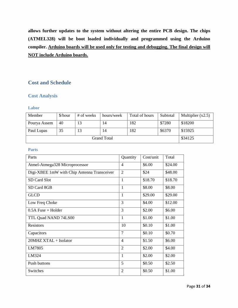
Labor
Member $/hour # of weeks hours/week Total of hours Subtotal Multiplier (x2.5)
Pourya Assem 40 13 14 182 $7280 $18200
Paul Lupas 35 13 14 182 $6370 $15925
Grand Total $34125
Parts
Parts Quantity Cost/unit Total
Atmel-Atmega328 Microprocessor 4 $6.00 $24.00
Digi-XBEE 1mW with Chip Antenna Transceiver 2 $24 $48.00
SD Card Slot 1 $18.70 $18.70
SD Card 8GB 1 $8.00 $8.00
GLCD 1 $29.00 $29.00
Low Freq Choke 3 $4.00 $12.00
0.5A Fuse + Holder 3 $2.00 $6.00
TTL Quad NAND 74LS00 1 $1.00 $1.00
Resistors 10 $0.10 $1.00
Capacitors 7 $0.10 $0.70
20MHZ XTAL + Isolator 4 $1.50 $6.00
LM7805 2 $2.00 $4.00
LM324 1 $2.00 $2.00
Push buttons 5 $0.50 $2.50
Switches 2 $0.50 $1.00

Page 32 of 34
PCB 2 $15.00 $30.00
Grand Total $193.90
Note: Cost of purchased items as of today $118.00
Grand Total
Labor Parts Grand Total
$34125 $193.90 $34318.90
Schedule
Week Task Member Assigned
9/2 Work on RFA Paul & Pourya
9/9 Work on Proposal
Research XBEE Transceiver
Research GCLD/Choke/ Fuse
Update Project Page
Paul & Pourya
Paul
Pourya
Paul & Pourya
9/16 Order GLCD and XBEE
Order SD Card Slot
Verify Proposal & Submission
Chokes: Assemble and Test
Pourya
Paul
Paul & Pourya
Pourya
9/23 Transmit and Receive data via XBEE
Test SD Card
Boot-Load Atmel-Atmega328 MP
Research Amplifiers
Amplifier: Design, Assemble and Test
Pourya
Paul
Pourya
Paul
Paul & Pourya
9/30 Slicers & Buffer: Assemble Test
Design Sign-up
LP Filter: Assemble and Test
Put it together
Pourya
Paul
Paul & Pourya
Paul & Pourya
10/7 Start Designing PCB
Research Power Supply
Power Supply: Design, Assemble and Test
Paul
Pourya
Paul & Pourya
10/14 Finish PCB Design
Start Programming the TX MP
Test TX MP, Coupled with XBEE
Paul & Pourya
Pourya
Paul
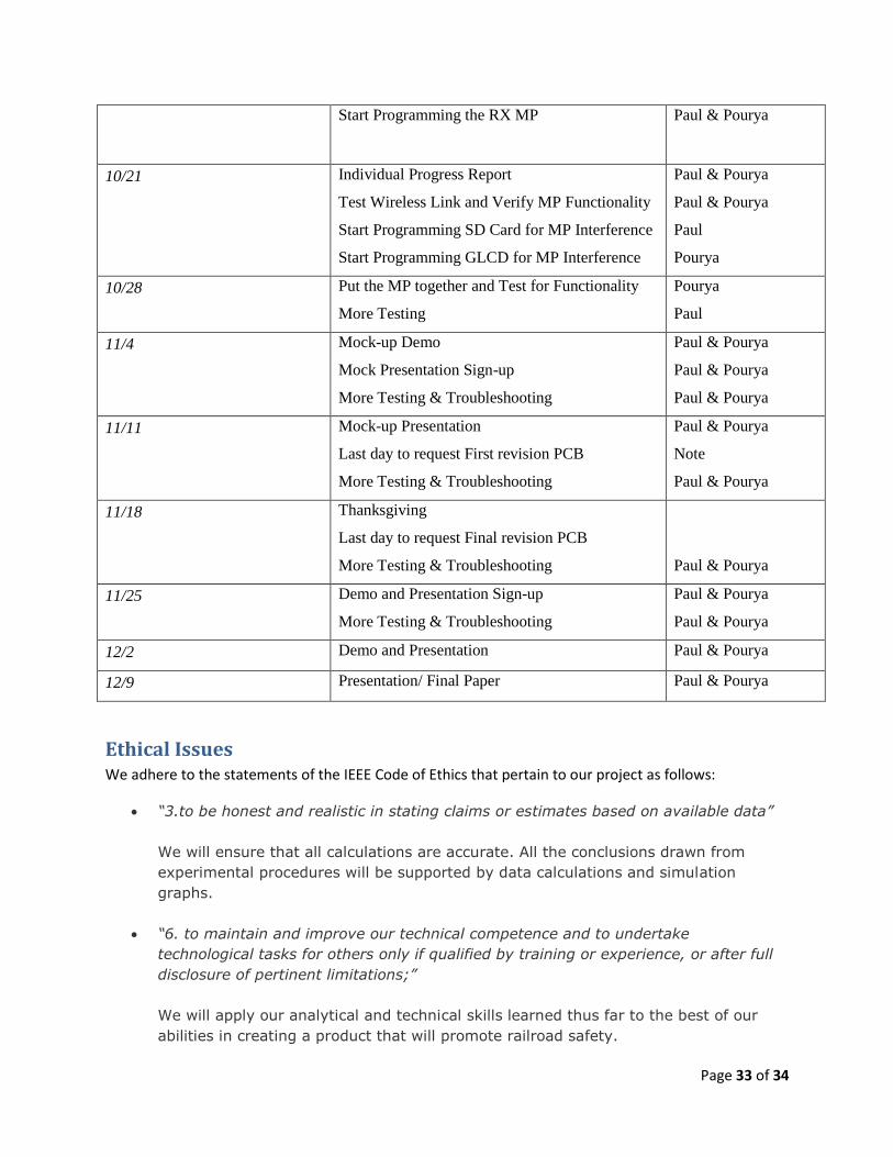
Page 33 of 34
Start Programming the RX MP Paul & Pourya
10/21 Individual Progress Report
Test Wireless Link and Verify MP Functionality
Start Programming SD Card for MP Interference
Start Programming GLCD for MP Interference
Paul & Pourya
Paul & Pourya
Paul
Pourya
10/28 Put the MP together and Test for Functionality
More Testing
Pourya
Paul
11/4 Mock-up Demo
Mock Presentation Sign-up
More Testing & Troubleshooting
Paul & Pourya
Paul & Pourya
Paul & Pourya
11/11 Mock-up Presentation
Last day to request First revision PCB
More Testing & Troubleshooting
Paul & Pourya
Note
Paul & Pourya
11/18 Thanksgiving
Last day to request Final revision PCB
More Testing & Troubleshooting
Paul & Pourya
11/25 Demo and Presentation Sign-up
More Testing & Troubleshooting
Paul & Pourya
Paul & Pourya
12/2 Demo and Presentation Paul & Pourya
12/9 Presentation/ Final Paper Paul & Pourya
Ethical Issues We adhere to the statements of the IEEE Code of Ethics that pertain to our project as follows:
“3.to be honest and realistic in stating claims or estimates based on available data”
We will ensure that all calculations are accurate. All the conclusions drawn from
experimental procedures will be supported by data calculations and simulation
graphs.
“6. to maintain and improve our technical competence and to undertake
technological tasks for others only if qualified by training or experience, or after full
disclosure of pertinent limitations;”
We will apply our analytical and technical skills learned thus far to the best of our
abilities in creating a product that will promote railroad safety.

Page 34 of 34
“7. to seek, accept, and offer honest criticism of technical work, to acknowledge
and correct errors, and to credit properly the contributions of others.”
Because this is a group project, each person will communicate his ideas on improving
the design and provide feedback on the other person’s work in terms of quality and
things that need improvement. In addition, all information used from outside sources
will be credited in the Reference Materials section.
References
"4D Systems, Research and Development." 4D Systems, Research and Development. N.p., n.d.
Web. 29 Sept. 2012. <http://www.4dsystems.com.au/>.
Boot loading procedures for the ATMEL328 microprocessor: Courtesy of CN RR, authored by
Pourya Assem
Component datasheets available upon request
Faludi, Robert. Building Wireless Sensor Networks: With ZigBee, XBee, Arduino, and
Processing. Farnham: O'Reilly, 2010. Print.
Fig.1, Fig.2 and Fig.3: Courtesy of CN RR authorized by Pourya Assem
"Micro SD Card Tutorial - Using SD Cards with an Arduino!" Micro SD Card Tutorial - Using
SD Cards with an Arduino! N.p., n.d. Web. 29 Sept. 2012.
<http://www.ladyada.net/products/microsd/>.
Sedra, Adel S., and Kenneth Carless. Smith. Microelectronic Circuits. 6th ed. New York: Oxford
UP, 2010. Print.
"T R O N I X S T U F F." T R O N I X S T U F F. N.p., n.d. Web. 29 Sept. 2012.
<http://tronixstuff.wordpress.com/>.