on-glass digital-to-analog converter with gamma correction
TRANSCRIPT

On-Glass Digital-to-Analog Converter with Gamma Correction for Panel Data Driver
Tzu-Ming Wang, Yu-Hsuan Li, and Ming-Dou Ker Nanoelectronics and Gigascale Systems Laboratory
Institute of Electronics, National Chiao-Tung University 1001 Ta-Hsueh Road, Hsinchu, Taiwan 300, R.O.C.
Abstract—An on-glass 6-bit R-string digital-to-analog converter (DAC) with gamma correction for panel data driver is proposed. The proposed circuit ,which is composed of folded R-string circuit, segmented digital decoder, and reordering decoding circuit, has been designed and fabricated in a 3-μm low-temperature poly-Si (LTPS) technology. The area of the proposed circuit is effectively reduced to about one sixth compared with the conventional one.
I. INTRODUCTION Low-temperature poly-silicon (LTPS) thin-film transistors
(TFTs) have been widely used for portable systems, such as digital camera, mobile phone, personal digital assistants (PDAs), notebook, and so on. The electron mobility of LTPS TFTs is about 100 times larger than that of the conventional amorphous silicon TFTs [1], so LTPS technology can achieve slim, compact, and high-resolution display by integrating the driver circuits on peripheral area of display. This LTPS technology will become more suitable for realization of system-on-panel (SOP) applications [2].
The periphery circuit blocks of LCD panel are roughly composed of four parts — display panel, timing control circuit, scan driver circuit, and data driver circuit [3]. Fig. 1 shows the block diagram of the TFT-LCD panel circuits. Display panel is constructed of the active matrix liquid crystals and the operation of the active matrixes is similar to DRAM (dynamic random access memory) which is used to charge and discharge the capacitor of the pixel. Timing control circuit is responsible for transmitting RGB (red, green, and blue) signals to the data driver and controlling the behavior of scan driver. As soon as one voltage level of the scan lines rises, the RGB signals are transmitted through the data driver. After a period, the voltage level of this scan line is disabled and next scan line is turned on. All voltage levels of those scan lines are raised in turn.
Scan driver circuit consists of shifter register, level shifter, and digital output buffer. Shifter register is used to store digital input signals then transit to the next stage according to timing control circuit. Because the turn-on voltage of active matrixes is higher, scan driver should drive the active pixels with a high voltage. The purpose of the level shifter is to convert the digital signal to higher voltage level. Finally, since
the scan lines can be modeled as RC (resister and capacitor) ladder, the digital output buffer should be used in the last stage for driving the large load.
Data driver circuit is composed of shifter register, data latch, level shifter, digital-to-analog converter (DAC), and analog output buffer. The first three parts classify as digital architectures, and the other two parts belong to analog architectures. Shifter register and data latch manage to transit and store the RGB signals. Also, the purpose of level shifter is the same as the one in scan driver circuit, which is applied to translate the RGB signal to a higher level voltage. In addition, digital-to-analog converter is used to convert the digital RGB signal to analog gray level. The analog output buffer is applied to drive active pixels into a desired gray level. However, the LCD panel usually has large load, especially in larger panel display or higher resolution display, so the analog output buffer should enhance the driving capability of the data driver.
Currently, LTPS technology has a tendency towards integrating all control circuits and driver circuits on the glass substrate [4], [5]. However, the poly-Si TFTs suffered poor uniformity with large variations on the device characteristics due to the narrow laser process window for producing large-grained poly-Si TFTs. The device variation becomes a serious problem for analog circuit realization on the LCD panel [6]. For this reason, the design of on-panel analog circuits is a challenge for SOP applications.
Figure 1. The block diagram of TFT-LCD panel circuits.
978-1-4244-2182-4/08/$25.00 ©2008 IEEE. 202
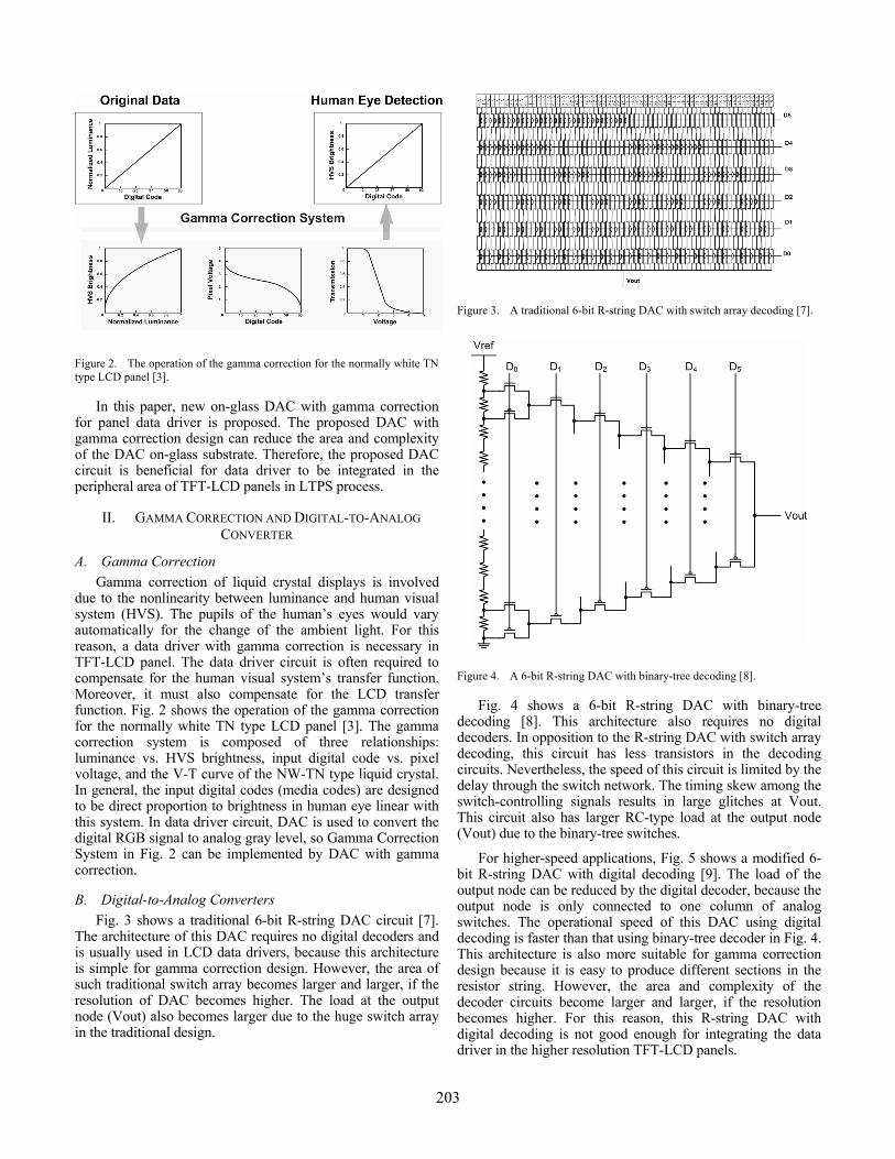
Figure 2. The operation of the gamma correction for the normally white TN type LCD panel [3].
In this paper, new on-glass DAC with gamma correction for panel data driver is proposed. The proposed DAC with gamma correction design can reduce the area and complexity of the DAC on-glass substrate. Therefore, the proposed DAC circuit is beneficial for data driver to be integrated in the peripheral area of TFT-LCD panels in LTPS process.
II. GAMMA CORRECTION AND DIGITAL-TO-ANALOG CONVERTER
A. Gamma Correction Gamma correction of liquid crystal displays is involved
due to the nonlinearity between luminance and human visual system (HVS). The pupils of the human’s eyes would vary automatically for the change of the ambient light. For this reason, a data driver with gamma correction is necessary in TFT-LCD panel. The data driver circuit is often required to compensate for the human visual system’s transfer function. Moreover, it must also compensate for the LCD transfer function. Fig. 2 shows the operation of the gamma correction for the normally white TN type LCD panel [3]. The gamma correction system is composed of three relationships: luminance vs. HVS brightness, input digital code vs. pixel voltage, and the V-T curve of the NW-TN type liquid crystal. In general, the input digital codes (media codes) are designed to be direct proportion to brightness in human eye linear with this system. In data driver circuit, DAC is used to convert the digital RGB signal to analog gray level, so Gamma Correction System in Fig. 2 can be implemented by DAC with gamma correction.
B. Digital-to-Analog Converters Fig. 3 shows a traditional 6-bit R-string DAC circuit [7].
The architecture of this DAC requires no digital decoders and is usually used in LCD data drivers, because this architecture is simple for gamma correction design. However, the area of such traditional switch array becomes larger and larger, if the resolution of DAC becomes higher. The load at the output node (Vout) also becomes larger due to the huge switch array in the traditional design.
Figure 3. A traditional 6-bit R-string DAC with switch array decoding [7].
Figure 4. A 6-bit R-string DAC with binary-tree decoding [8].
Fig. 4 shows a 6-bit R-string DAC with binary-tree decoding [8]. This architecture also requires no digital decoders. In opposition to the R-string DAC with switch array decoding, this circuit has less transistors in the decoding circuits. Nevertheless, the speed of this circuit is limited by the delay through the switch network. The timing skew among the switch-controlling signals results in large glitches at Vout. This circuit also has larger RC-type load at the output node (Vout) due to the binary-tree switches.
For higher-speed applications, Fig. 5 shows a modified 6-bit R-string DAC with digital decoding [9]. The load of the output node can be reduced by the digital decoder, because the output node is only connected to one column of analog switches. The operational speed of this DAC using digital decoding is faster than that using binary-tree decoder in Fig. 4. This architecture is also more suitable for gamma correction design because it is easy to produce different sections in the resistor string. However, the area and complexity of the decoder circuits become larger and larger, if the resolution becomes higher. For this reason, this R-string DAC with digital decoding is not good enough for integrating the data driver in the higher resolution TFT-LCD panels.
203
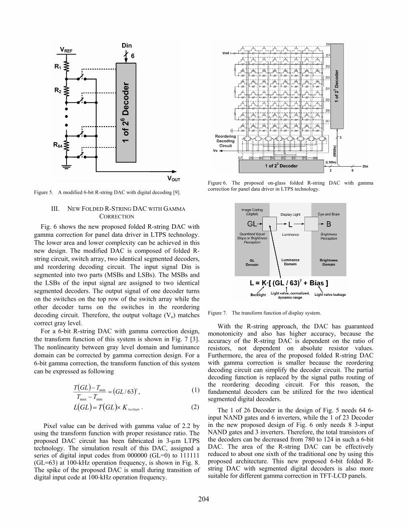
Figure 5. A modified 6-bit R-string DAC with digital decoding [9].
III. NEW FOLDED R-STRING DAC WITH GAMMA CORRECTION
Fig. 6 shows the new proposed folded R-string DAC with gamma correction for panel data driver in LTPS technology. The lower area and lower complexity can be achieved in this new design. The modified DAC is composed of folded R-string circuit, switch array, two identical segmented decoders, and reordering decoding circuit. The input signal Din is segmented into two parts (MSBs and LSBs). The MSBs and the LSBs of the input signal are assigned to two identical segmented decoders. The output signal of one decoder turns on the switches on the top row of the switch array while the other decoder turns on the switches in the reordering decoding circuit. Therefore, the output voltage (Vo) matches correct gray level.
For a 6-bit R-string DAC with gamma correction design, the transform function of this system is shown in Fig. 7 [3]. The nonlinearity between gray level domain and luminance domain can be corrected by gamma correction design. For a 6-bit gamma correction, the transform function of this system can be expressed as following
( ) ( ) ,63/
minmax
min γGLTTTGLT
=−− (1)
( ) ( ) backlightKGLTGLL ×= . (2)
Pixel value can be derived with gamma value of 2.2 by
using the transform function with proper resistance ratio. The proposed DAC circuit has been fabricated in 3-μm LTPS technology. The simulation result of this DAC, assigned a series of digital input codes from 000000 (GL=0) to 111111 (GL=63) at 100-kHz operation frequency, is shown in Fig. 8. The spike of the proposed DAC is small during transition of digital input code at 100-kHz operation frequency.
Figure 6. The proposed on-glass folded R-string DAC with gamma correction for panel data driver in LTPS technology.
Figure 7. The transform function of display system.
With the R-string approach, the DAC has guaranteed monotonicity and also has higher accuracy, because the accuracy of the R-string DAC is dependent on the ratio of resistors, not dependent on absolute resistor values. Furthermore, the area of the proposed folded R-string DAC with gamma correction is smaller because the reordering decoding circuit can simplify the decoder circuit. The partial decoding function is replaced by the signal paths routing of the reordering decoding circuit. For this reason, the fundamental decoders can be utilized for the two identical segmented digital decoders.
The 1 of 26 Decoder in the design of Fig. 5 needs 64 6-input NAND gates and 6 inverters, while the 1 of 23 Decoder in the new proposed design of Fig. 6 only needs 8 3-input NAND gates and 3 inverters. Therefore, the total transistors of the decoders can be decreased from 780 to 124 in such a 6-bit DAC. The area of the R-string DAC can be effectively reduced to about one sixth of the traditional one by using this proposed architecture. This new proposed 6-bit folded R-string DAC with segmented digital decoders is also more suitable for different gamma correction in TFT-LCD panels.
204
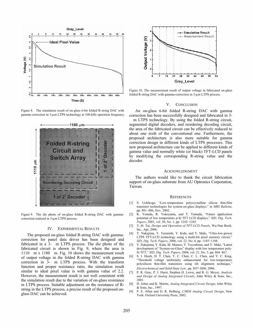
Figure 8. The simulation result of on-glass 6-bit folded R-string DAC with gamma correction in 3-μm LTPS technology at 100-kHz operation frequency.
Figure 9. The die photo of on-glass folded R-string DAC with gamma-correction realized in 3-μm LTPS process.
IV. EXPERIMENTAL RESULTS The proposed on-glass folded R-string DAC with gamma-
correction for panel data driver has been designed and fabricated in a 3- m LTPS process. The die photo of the fabricated circuit is shown in Fig. 9, where the area is 1110 m x 1180 m. Fig. 10 shows the measurement result of output voltage in the folded R-string DAC with gamma correction in 3- m LTPS process. With the transform function and proper resistance ratio, the simulation result similar to ideal pixel value is with gamma value of 2.2. However, the measurement result is not well consistent with the simulation result due to the variation of on-glass resistance in LTPS process. Suitable adjustment on the resistance of R-string in the LTPS process, a precise result of the proposed on-glass DAC can be achieved.
Figure 10. The measurement result of output voltage in fabricated on-glass folded R-string DAC with gamma-correction in 3-μm LTPS process.
V. CONCLUSION An on-glass 6-bit folded R-string DAC with gamma
correction has been successfully designed and fabricated in 3- m LTPS technology. By using the folded R-string circuit, segmented digital decoders, and reordering decoding circuit, the area of the fabricated circuit can be effectively reduced to about one sixth of the conventional one. Furthermore, the proposed architecture is also more suitable for gamma correction design in different kinds of LTPS processes. This new proposed architecture can be applied to different kinds of gamma value and normally white (or black) TFT-LCD panels by modifying the corresponding R-string value and the decoder.
ACKNOWLEDGMENT The authors would like to thank the circuit fabrication
support of on-glass substrate from AU Optronics Corporation, Taiwan.
REFERENCES [1] S. Uchikoga, “Low-temperature polycrystalline silicon thin-film
transistor technologies for system-on-glass displays,” in MRS Bulletin, pp. 881−886, Nov. 2002.
[2] K. Yoneda, R. Yokoyama, and T. Yamada, “Future application potential of low temperature p-Si TFT LCD displays,” SID, Dig. Tech. Papers, 2001, vol. 50, No. 1, pp. 1242−1245.
[3] Y.-H. Tai, Design and Operation of TFT-LCD Panels, Wu-Nan Book, Inc., Apr. 2006.
[4] Y. Nakajima, Y. Teranishi, Y. Kida, and Y. Maki, “Ultra-low-power LTPS TFT-LCD technology using a multi-bit pixel memory circuit,” SID, Dig. Tech. Papers, 2006, vol. 22, No. 4, pp. 1185−1188.
[5] Y. Nakajima, Y. Kida, M. Murase, Y. Toyoshima, and Y. Maki, “Latest development of “System-on-Glass” display with low temperature poly-Si TFT,” SID, Dig. Tech. Papers, 2004, vol. 21, No. 3, pp. 864−867.
[6] S. I. Hsieh, H. T. Chen, Y. C. Chen, C. L. Chen, and Y. C. King, “Threshold voltage uniformity enhancement for low-temperature polysilicon thin-film transistors using tilt alignment technique,” Electrochemical and Solid-State Lett., pp. H57–H60, 2006.
[7] P. R. Gray, P. J. Hurst, Stephen H. Lewis, and R. G. Meyer, Analysis and Design of Analog Integrated Circuits, John Wiley & Sons, Inc., 2001.
[8] D. Johns and K. Martin, Analog Integrated Circuit Design, John Wiley & Sons, Inc., 1997.
[9] P. E. Allen and D. R. Holberg, CMOS Analog Circuit Design, New York: Oxford University Press, 2002.
205