on-chip optical stabilization of high-speed mode-locked
TRANSCRIPT

University of Central Florida University of Central Florida
STARS STARS
Electronic Theses and Dissertations, 2004-2019
2014
On-Chip Optical Stabilization of High-Speed Mode-locked On-Chip Optical Stabilization of High-Speed Mode-locked
Quantum Dot Lasers for Next Generation Optical Networks Quantum Dot Lasers for Next Generation Optical Networks
Abhijeet Ardey University of Central Florida
Part of the Physics Commons
Find similar works at: https://stars.library.ucf.edu/etd
University of Central Florida Libraries http://library.ucf.edu
This Doctoral Dissertation (Open Access) is brought to you for free and open access by STARS. It has been accepted
for inclusion in Electronic Theses and Dissertations, 2004-2019 by an authorized administrator of STARS. For more
information, please contact [email protected].
STARS Citation STARS Citation Ardey, Abhijeet, "On-Chip Optical Stabilization of High-Speed Mode-locked Quantum Dot Lasers for Next Generation Optical Networks" (2014). Electronic Theses and Dissertations, 2004-2019. 4735. https://stars.library.ucf.edu/etd/4735

ON-CHIP OPTICAL STABILIZATION OF HIGH-SPEED MODE-LOCKED QUANTUM DOT LASERS FOR NEXT GENERATION OPTICAL NETWORKS
by
ABHIJEET DILIP ARDEY B.S. University of Delhi, 2001 M.S. University of Delhi, 2003
M.S. University of Central Florida, 2007
A dissertation submitted in partial fulfillment of the requirements for the degree of Doctor of Philosophy
in the Department of Physics in the College of Sciences
at the University of Central Florida Orlando, Florida
Summer Term 2014
Major Professor: Peter J. Delfyett, Jr.

© 2014 Abhijeet Ardey
ii

ABSTRACT
Monolithic passively mode-locked colliding pulse semiconductor lasers generating
pico- to sub-picosecond terahertz optical pulse trains are promising sources for future
applications in ultra-high speed data transmission systems and optical measurements.
However, in the absence of external synchronization, these passively mode-locked lasers
suffer from large amplitude and timing jitter instabilities resulting in broad comb
linewidths, which precludes many applications in the field of coherent communications
and signal processing where a much narrower frequency line set is needed.
In this dissertation, a novel quantum dot based coupled cavity laser is presented,
where for the first time, four-wave mixing (FWM) in the monolithically integrated
saturable absorber is used to injection lock a monolithic colliding pulse mode-locked (CPM)
laser with a mode-locked high-Q ring laser. Starting with a passively mode-locked master
ring laser, a stable 30 GHz optical pulse train is generated with more than 10 dB reduction
in the RF noise level at 20 MHz offset and close to 3-times reduction in the average optical
linewidth of the injection locked CPM slave laser. The FWM process is subsequently
verified experimentally and conclusively shown to be the primary mechanism responsible
for the observed injection locking. Other linear scattering effects are found to be negligible,
as predicted in the orthogonal waveguide configuration. The novel injection locking
technique is further exploited by employing optical hybrid mode-locking and increasing
the Q of the master ring cavity, to realize an improved stabilization architecture. Dramatic
reduction is shown with more than 14-times reduction in the photodetected beat linewidth
and almost 5-times reduction in the optical linewidth of the injection locked slave laser
with generation of close to transform limited pulses at ~ 30 GHz. These results demonstrate
iii

the effectiveness of the novel injection locking technique for an all-on-chip stability
transfer and provides a new way of stabilizing monolithic optical pulse sources for
applications in future high speed optical networks.
iv

This work is dedicated to my family for their constant support and unconditional love.
v

ACKNOWLEDGMENTS
I would like to thank my advisor, Prof. Peter Delfyett who believed in me and
without whose support none of what follows would have been possible. His patience,
motivation and enthusiasm guided me through the most difficult times while writing my
dissertation. I could not have imagined a better advisor and mentor for my Ph.D. study.
I would also like to thank the entire Ultrafast Photonics group, members past and
present, for their support that helped make this work possible. They are Dr. Sangyoun Gee,
Dr. Franklyn Quinlan, Dr. Sarper Ozharar, Dr. Jimyung Kim, Dr. Ibrahim Ozdur, Dr.
Dimitrios Mandridis, Dr. Mohammad Umar Piracha, Dr. Mehmetcan Akbulut, Dr. Nishant
Bhatambrekar, Dr. Nazanin Hoghooghi, Dr. Josue Davila-Rodriguez, Dr. Charles Williams,
Dr. Dat Nguyen, Sharad Bhooplapur, Marcus Bagnell, Edris Sarailou, Anthony Klee and
Kristina Bagnell.
vi

TABLE OF CONTENTS
LIST OF FIGURES ........................................................................................................... ix
LIST OF TABLES ........................................................................................................... xiv
LIST OF ACRONYMS/ABBREVIATIONS ................................................................... xv
CHAPTER 1 INTRODUCTION ........................................................................................ 1
1.1 Mode-locked lasers ................................................................................................... 3
1.2 Colliding pulse mode-locked lasers .......................................................................... 5
1.3 Quantum dot based mode-locked lasers ................................................................... 7
CHAPTER 2 NOVEL QUANTUM DOT BASED COUPLED-CAVITY COLLIDING
PULSE MODE-LOCKED LASER .................................................................................... 9
2.1 Sub-harmonic optical injection locking .................................................................. 10
2.2 Novel device design concept .................................................................................. 10
2.3 Device design and fabrication ................................................................................. 12
2.3.1 Fabrication procedure ...................................................................................... 17
2.3.2 Broadband anti-reflection coatings .................................................................. 24
2.4 Experimental setup.................................................................................................. 32
2.5 Measurement and results ......................................................................................... 34
CHAPTER 3 CONFIRM FOUR-WAVE MIXING PROCESS AS THE PRIMARY
INJECTION LOCKING MECHANISM .......................................................................... 40
3.1 Experimental setup.................................................................................................. 41
3.2 Measurement and results ......................................................................................... 43
CHAPTER 4 IMPROVED STABILIZATION ARCHITECTURE ................................. 48
4.1 Experimental setup.................................................................................................. 49
vii

4.2 Measurement and results ......................................................................................... 52
CHAPTER 5 FUTURE ALL MONOLITHIC DESIGN .................................................. 59
5.1 Using optical hybrid mode-locking ........................................................................ 60
5.2 Using RF hybrid mode-locking .............................................................................. 63
CHAPTER 6 CONCLUSION........................................................................................... 64
APPENDIX A C++ CODE USED FOR MASK LAYOUT ............................................. 66
APPENDIX B PECVD RECIPE FILES........................................................................... 75
REFERENCES ................................................................................................................. 81
viii

LIST OF FIGURES
Figure 1: Schematic of a monolithic colliding pulse mode-locked (CPM) laser. ............... 6
Figure 2: Schematic of the multi-section device. It also illustrates the four-wave mixing
process....................................................................................................................... 11
Figure 3: A schematic illustrating the QD wafer structure. .............................................. 12
Figure 4: (Left): Fabricated device before metallization with BCB as the isolation layer
(seen in green). (Right): Magnified picture showing crossed saturable absorbers,
each being 200 μm in length. .................................................................................... 14
Figure 5: Photomask parameters of the curved two-section device. ................................ 15
Figure 6: Photomask parameters of the semiconductor optical amplifier (SOA) device. 15
Figure 7: Bars of (two not cleaved bars consisting of nine devices each) fabricated SOAs
before cleaving. ......................................................................................................... 16
Figure 8: Schematic illustrating positive photolithography steps. .................................... 17
Figure 9: Mesa ridge-waveguides are formed in a single wet-etching step. ..................... 18
Figure 10: BCB polymer is used as the dielectric insulation layer. .................................. 19
Figure 11: Schematic illustrating negative photolithography steps for depositing p-side
metal contacts............................................................................................................ 20
Figure 12: P-side metallization is followed by annealing at 400°C. ................................ 21
Figure 13: The wafer is lapped and polished to a thickness of ~ 150 μm before cleaving
into individual devices from the device bar. ............................................................. 21
Figure 14: After n-side metallization and annealing at 400°C, individual devices are
cleaved and mounted on gold-coated copper studs................................................... 22
Figure 15: SEM image of the facet of a fabricated device. .............................................. 23
ix

Figure 16: Multi-section device mounted inside the setup. Shown below are SOAs
mounted on gold coated copper studs. ...................................................................... 24
Figure 17: Reflectance diagram (for s-polarization). ........................................................ 26
Figure 18: Admittance diagram (for s-polarization). ........................................................ 27
Figure 19: Calculated reflectance and transmittance (for s-polarization) of the 3-layer
coating. Reflectance is shown using bold line. ......................................................... 27
Figure 20: Calculated reflectance as a function of incident angle. ................................... 28
Figure 21: LI-IV curves of the 1.5 mm Fabry-perot laser before and after AR coating. .. 29
Figure 22: Measured reflectivity of the coated fabry-perot laser (λc = 1270 nm) using
Kaminow-Eisenstein method. Also shown is the optical spectrum with no lasing
seen even at higher injection currents. ...................................................................... 30
Figure 23: Delrim fixture with a bar of SOAs for AR coating ......................................... 31
Figure 24: Graph showing the gain comparison of the coated and uncoated SOAs......... 31
Figure 25: Schematic drawing of the experimental setup. SOA, semiconductor optical
amplifier; BS, pellicle beam splitter (92-8%); λ/2, half-wave plate; ISO, optical
isolator; OSA, optical spectrum analyzer. ................................................................ 33
Figure 26: Spectra of the passively mode-locked high-Q external cavity (master) laser: (a)
Optical spectrum, (b) RF power spectrum showing 66th harmonic, (c)
Autocorrelation trace, (d) Optical linewidth, measured using the self-heterodyne
setup. ......................................................................................................................... 35
Figure 27: Schematic drawing of the delayed self-heterodyne setup used to measure the
optical linewidth of both lasers. SOA, semiconductor optical amplifier; AOM,
acousto-optic modulator; PC, polarization controller; PD, photodetector. ............... 36
x

Figure 28: Spectra of the passively mode-locked CPM (slave) laser before (in blue) and
after (in red) optical injection: (a) Optical spectrum before injection, (b) Optical
spectrum after injection, (c) Comparison of RF power spectrum showing almost 5-
times reduction in the 30 dB RF linewidth after injection, (d) Autocorrelation trace,
remains indistinguishable after injection locking (e) Optical linewidth before
injection, (f) Optical linewidth after injection showing close to 3-times reduction in
the 10 dB optical linewidth. ...................................................................................... 38
Figure 29: Schematic of the experimental setup to confirm four-wave mixing (FWM).
The horizontal and vertical polarized light is shown using symbols H and V,
respectively. The symbol Hb and Vb denote the polarization of the backward emitted
ASE light in the counter-clockwise direction. The output ports of the external ring
laser are marked as 1 and 2, respectively. ASE, amplified spontaneous emission;
SOA, semiconductor optical amplifier; Pol, linear polarizer; PBS, polarizing beam
splitter; FR, faraday rotator; BS, pellicle beam splitter; λ/2, half-wave plate; ISO,
optical isolator. .......................................................................................................... 42
Figure 30: (a), (b): Typical spectra of the passively mode-locked high-Q external cavity
(master) laser. (c), (d): Typical spectra of the passively mode-locked CPM (slave)
laser before (in blue) and after (in red) optical injection. ......................................... 44
Figure 31: (a): Backward propagating ASE spectra from port-2 of the passively mode-
locked high-Q external cavity (master) laser with and without injection of the CPM
laser. Also seen is the back reflected leakage light from the intra-cavity optics
superimposed on the ASE spectra. (b): Background subtracted spectra from Fig.
31(a), showing the diffracted CPM spectra present in port-2 due to FWM. (c): ASE
xi

spectra from port-2 of the master laser with port-1 physically blocked. (d):
Background subtracted spectra from Fig. 31(c), with no residual CPM laser light
observed in the absence of FWM. ............................................................................. 46
Figure 32: A schematic of the experimental setup. CPM: colliding pulse mode-locked
slave laser, λ/2: half-wave plate, BS: beam splitter. ................................................. 50
Figure 33: Delayed self-heterodyne setup used for optical linewidth measurement with 1-
km of optical fiber. .................................................................................................... 51
Figure 34: Spectra of the hybridly mode-locked (3rd harmonic mode-locking) high-Q
external cavity (master) laser. ................................................................................... 53
Figure 35: Optical spectral overlap of the slave and master laser achieved by tuning the
device temperature (~18 º to 19 º C). ........................................................................ 54
Figure 36: Optical linewidth variation of master ring-cavity with bias-conditions and
temperature. .............................................................................................................. 55
Figure 37: Spectra of the passively mode-locked CPM (slave) laser before (in blue) and
after (in red) optical injection via four-wave mixing. ............................................... 57
Figure 38: Autocorrelation trace and the measured pulse-width of the CPM laser. ......... 58
Figure 39: Illustration of all monolithically integrated novel design with epitaxial III-V
gain material metal-bonded within SOI platform. The design would incorporate low-
loss Si3N4 waveguides in the case of high-Q ring cavity which is then modulated
with EA modulator (III-V based) for low-noise hybrid mode-locking..................... 61
Figure 40: Cross-section view of the geometry of the future all monolithically integrated
design. ....................................................................................................................... 62
xii

Figure 41: Cross-section view of the monolithic device with linear Si3N4 waveguides for
the high-Q cavity and tunable distributed Bragg reflector (DBR) mirrors. The
heaters together with DBR mirrors would serve as the phase tuning element for
longitudinal optical mode overlap of the two crossed laser cavities for optimal
injection locking........................................................................................................ 63
xiii

LIST OF TABLES
Table 1: InAs/InGaAs quantum dot wafer structure (courtesy Innolume GmbH). .......... 13
Table 2: Photomask parameters for the curved and saturable absorber sections in the
multi-section device. ................................................................................................. 15
Table 3: Hardcure temperature profile. ............................................................................. 19
Table 4: Anti-reflection coating parameters (reference wavelength λ = 1310 nm). ......... 25
Table 5: Comparison of silicon modulators (ref. [35]). .................................................... 62
xiv

LIST OF ACRONYMS/ABBREVIATIONS
AR Anti-Reflection
AOM Acousto-Optic Modulator
ASE Amplified Spontaneous Emission
BCB Benzocyclobutene
BS Beam Splitter
CPM Colliding Pulse Mode-locked laser
CW Continuous Wave
EAM Electro-absorption modulator
FP Fabry-Pérot
FSR Free Spectral Range
FWM Four-Wave Mixing
ISO Optical Isolator
IV Current output Versus Voltage
LEF Linewidth Enhancement Factor
LI Light output Versus Current
MZI Mach-Zehnder Interferometer
OTDM Optical Time-Division Multiplexing
PBS Polarizing Beam Splitter
PC Polarization Controller
PD Photodetector
PECVD Plasma Enhanced Chemical Vapor Deposition
POL Polarizer
xv

QD Quantum Dot
QW Quantum Well
RF Radio Frequency
RIE Reative-ion Etching
RTA Rapid Thermal Annealing
SA Saturable Absorber
SEM Scanning Electron Microscope
SMF Single Mode Fiber
SOA Semiconductor Optical Amplifier
SOI Silicon on Insulator
TBP Time-Bandwidth Product
TE Transverse Electric
TEC Thermo-Electric Cooler
UV Ultraviolet
xvi

CHAPTER 1 INTRODUCTION
Light sources generating short optical pulses at high repetition frequencies are the
key components for future large capacity optical communication networks. These include
high-bit-rate optical time-division multiplexing (OTDM) systems and microwave &
millimeter-wave photonic systems [1], [2]. Infact lasers operating at tens of gigahertz
repetition rates are already being implemented in high-capacity telecommunication
systems, photonics switching devices and clocks for very-large-scale integrated
microprocessors. High-frequency short optical pulses generated are also being used for
ultrafast optical measurements, such as electro-optic sampling and optical analogue to
digital conversion. In recent years, monolithic mode-locked semiconductor lasers have
attracted considerable attention for these photonic applications. These mechanically stable
and cost-effective laser diodes have excellent pulse characteristics over other optical pulse
sources including high repetition rates, short pulsewidths and small frequency chirp.
Monolithic passively mode-locked lasers, especially quantum dot (QD) based lasers with
unique characteristics, such as ultrabroad gain bandwidth, low threshold current, enhanced
temperature stability, low linewidth enhancement factor, and ultrafast gain and absorption
dynamics offer promise as compact, reliable and robust optical sources [3-5]. However, in
the absence of direct electrical modulation, these passively mode-locked lasers are
susceptible to large amplitude and timing jitter instabilities resulting in broad comb
linewidths, which precludes many applications in the field of coherent communications
and signal processing where a much narrower frequency line set is needed [6], [7]. Previous
research has been focused on the external stabilization of pulse trains such as optoelectronic
1
feedback using phase-locked loops, optical pulse injection, and sub-harmonic optical
injection [8-10]. Recently, optical micro-resonators have also been demonstrated to serve
as compact sources of optical frequency combs [11]. However, the complexity of all these
techniques, and the fabrication and cost involved, limit their applications.
In this Ph.D. dissertation, we present a novel and simple QD based multi-section
laser design where a stable high-Q passively mode-locked ring laser is used to injection
lock a passively mode-locked colliding pulse mode-locked (CPM) laser. CPM laser design
using an intracavity saturable absorber is chosen as it provides nearly transform limited
ultrafast optical pulse train without the need for high speed electronics. These lasers have
already been demonstrated to produce pico- to sub-picosecond pulses at repetition
frequencies from 16 to 480 GHz [12], [13]. Owing to the sparse nature of the QD material,
which results in low modal gain, the colliding pulse design is optimal as it avoids the need
for the impractical shortening of cavity length. In the novel laser design demonstrated,
four-wave mixing (FWM) in the common saturable absorber is used for injection locking,
which stabilizes and hence reduces the timing jitter as well as the long-term frequency drift
of the slave laser. A stable 30 GHz optical pulse train is generated and both the RF and
optical linewidths are significantly reduced confirming the effectiveness of the FWM
technique. This is the first time, to the best of our knowledge that FWM has been
conclusively shown to be used for injection locking in semiconductor media especially in
an orthogonal waveguide configuration. We also subsequently investigate the contributions
from other mechanisms such as linear scattering, which are found to be negligible as
expected in the case of low-index contrast perpendicular waveguide crossings. Finally we
show that by hybrid mode-locking the external ring cavity laser and decreasing the losses
2
in the high-Q cavity, the jitter values of the injected slave laser can be further reduced
making this ultra-compact and ultra-short optical pulse source attractive for use in the
forthcoming photonic access networks.
1.1 Mode-locked lasers
Short optical pulse diode lasers have been proposed using a wide range of schemes
such as gain switching, Q-Switching and mode-locking [14]. Gain switched and Q-
switched lasers are attractive since they do not require external cavities, are easy to operate
and have the flexibility of changing cavity repetition rate without modifying the cavity
length. However, they exhibit significant frequency chirp and timing jitter coupled with
wide pulsewidths and large time-bandwidth products. Mode-locked semiconductor lasers
facilitate short optical pulses with very pure spectral properties and low timing jitter [15].
In mode-locked lasers the pulse generation is through the phase locking of longitudinal
modes supported by the cavity with the repetition rate of the pulse-train defined by the
cavity length and the number of pulses circulating in the cavity. The monolithic cavity
designs reported thus have repetition rates from 10 to in excess of hundreds of GHz
depending on the cavity length and if whether harmonic mode-locking is implemented.
The simplest cavity configuration for mode-locking is the single-segment design
where direct electrical modulation is used to generate accurately timed pulses by
synchronizing the optical pulse train to systems clocks and also reduce the timing jitter.
This scheme is referred to active mode-locking. A stable microwave oscillator can be used
to modulate an intracavity gain, loss or phase element at the cavity round-trip frequency to
lock the longitudinal modes of the laser and produce short optical pulses. However, as you
can infer the optical pulse width in this case is determined by how narrow the electrical
3

modulation pulse widths are and parasitic capacitance of the device itself becomes an issue
at higher modulation frequencies. So although active mode-locking is the most
straightforward approach, its maximum frequency is limited to around 40 GHz.
On the other hand if the pulses can modulate the absorption on its own than the net
gain window generated by pulse can be as short as the pulse itself. Therefore passively
mode-locked lasers can generate shorter pulses than actively mode-locked lasers. The key
component in this scheme is an intensity dependent non-linear element called saturable
absorber which is responsible for the self-start of mode-locking. The saturable absorber
sharpens and narrows the pulses by preferentially passing the high energy peak of the
pulses with minimum loss. The pulse shaping process continues until limited by the pulse-
broadening mechanisms inside the cavity. Since the pulse shaping is determined by the
difference in saturating energies and recovery time constants between the gain and
saturable absorber, in case of passive mode-locking it is possible to generate short optical
pulses with a repetition rate beyond modulation bandwidths of the semiconductor lasers.
However, in the absence of an external reference clock these passively mode-locked lasers
suffer from large amplitude and timing jitter instabilities.
Hybrid mode-locking schemes have also been proposed which incorporate active
gain modulation along with passive gain modulation from saturable absorber offer the best
combination of the above mode-locking techniques. Here the saturable absorption is the
dominant mechanism for obtaining short optical pulsewidths while the active modulation
stabilizes the pulse stream in amplitude and time. In case of monolithic mode-locked lasers
all of these necessary functions of active, passive and hybrid mode-locked lasers can be
implemented together on a single semiconductor chip. However, the implementation of
4
this technique still becomes difficult as the repetition rate increases because of the
limitation of the drive electronics.
1.2 Colliding pulse mode-locked lasers
The pulse shaping mechanism can be more effective in case of colliding pulse
mode-locking scheme where instead of having a single pulse passing through the saturable
absorber at one time we have coherent interaction of two-counter propagating pulses which
collide in saturable absorber to generate ultrashort transform limited pulses. The
synchronization of the pulses to collide in the saturable absorber occurs because in this
case minimum energy is lost to the SA. When the two pulses collide, electric standing
waves are formed. The standing-wave intensity is quadruple the intensity of the individual
pulses as a result of constructive interference which results in twice as much energy density
saturating the absorber than the gain medium. Also the carrier density does not have to be
brought to transparency everywhere to allow the pulses to pass with low loss. This
enhanced effective saturation cross section of the absorber helps to stabilize and shorten
pulses. The two simultaneously counter-propagating pulses also lead to a doubling of the
repetition frequency as compared to a conventional mode-locked laser of the same length
giving rise to a high repetition rate pulse train without the need for an unpractical
shortening of the laser cavity length.
5

Figure 1: Schematic of a monolithic colliding pulse mode-locked (CPM) laser.
Another interaction in CPM is the formation of transient grating (often referred to
as degenerate four-wave mixing) due to the periodic carrier density variation in the
saturable absorber region because of the transient standing wave optical field [16], [17].
The carrier generation is high at the peak of the standing wave and low at the standing
wave minimum, forming an absorption grating. The grating can reduce the frequency chirp
in the mode-locked laser as those portions of the two colliding pulses which collide and
have non-equal zero-crossing spacing’s under the pulse envelope will not efficiently form
the carrier density grating. Thus pulses with frequency chirp encounter higher loss in the
saturable absorber compared with unchirped pulses leading to even shorter pulse widths
directly from the laser.
However, as in case of any passive mode-locked laser, the spontaneous emission
noise produces variations in the timing of each mode-locked pulse and thus increases the
6

timing jitter. Recent research has been focused towards stabilizing these lasers by either
reducing the parasitic capacitance by employing new novel gain materials or by electrical
or optical injection locking of these devices [18-20]. Considering the high repetition rates
of the monolithic CPM devices, direct modulating at high speeds is still problematic due
to the high RC time constants and optical injection locking calls for an external master laser
which leads to not so compact system to begin with together with coupling and stability
issues arising from having two physically separate lasers. Thus there is a need for a new
monolithic scheme which addresses these issues and can be practically implemented in a
single optoelectronic integrated circuit.
1.3 Quantum dot based mode-locked lasers
Semiconductor quantum dots, which demonstrate ultrabroad gain bandwidth,
ultrafast gain dynamics and easily saturated gain and absorption, have become one of the
most promising material systems for the generation of ultrashort pulses. The higher
dimensional confinement of QDs as compared to QW leads to an increased ratio of
saturation energies in the gain and absorber sections, which is a key parameter in mode-
locking. With an extremely broad emission spectrum of more than 100 nm, QD based
mode-locked lasers have the potential of generating ultrashort optical pulses. With
absorption recovery times as fast as 700 fs already shown, makes this material system an
ideal choice for generating high repetition rate optical pulses while the high gain saturation
energy facilitates the formation of high peak power pulses. The low threshold current
densities, low internal loss, and low confinement factor help to reduce noise. With lower
associated spontaneous emission noise as compared to quantum well (QW) devices, the
linewidths are generally narrower in QD lasers. The lowest timing jitter values reported so
7

far in case of mode-locked semiconductor lasers have been in the QD active media, thereby
confirming the importance of employing QD materials for future optical communication
systems [21]. The same above properties also make the QD material a good choice for
ultrafast amplification of these generated optical pulses across a relatively broad spectral
range. Ultrafast and distortion free amplification has been already reported at pulse
repetition rates of up to 80 GHz, for pulse durations down to 710 fs [22]. With the
additional inherent features of being temperature resilient, owing to the absence of higher
energy states that can be thermally populated and operation in telecom band of 1260-1360
nm, QD based mode-locked lasers have become suitable candidates for the next generation
optical networks.
8

CHAPTER 2 NOVEL QUANTUM DOT BASED COUPLED-CAVITY COLLIDING
PULSE MODE-LOCKED LASER
As mentioned previously, colliding pulse mode-locking in a semiconductor laser is
a very effective method for generating optical pulses in the pico to sub-picosecond range.
Monolithic CPM lasers are thermally and mechanically stable since there are no moving
parts. This together with the added benefits of passive mode-locking, which require no
external RF electrical source for pulse generation in principle, makes these lasers an ideal
source of highly repetitive optical pulse train without the limitation imposed by drive
electronics. However, in the absence of synchronization to an external source these
passively mode-locked lasers suffer from large phase noise, which limits there
implementation in optical communication systems, where with increasing data capacity
more stringent requirements on timing jitter are being imposed.
This chapter outlines a novel QD based coupled cavity laser, where a stable high-
Q master laser is used to injection lock a passively mode-locked monolithic colliding pulse
slave laser through four-wave mixing in the common saturable absorber. With an all
passive stabilization architecture, where both the CPM and high-Q master laser are
passively mode-locked, significant reduction in the RF and optical linewidths of the CPM
laser is shown. The device design and the fabrication processes involved are also discussed
in detail.
9

2.1 Sub-harmonic optical injection locking
Out of all the injection locking techniques presented recently, sub-harmonic optical
injection locking is the most promising to help stabilize a monolithic CPM laser. The
technique has obvious advantages over its electrical counterpart as there is no requirement
of an external RF source and also does not suffer from the resulting unwanted amplitude
modulation (arising from the cavity resonant effect). Stabilization of CPM cavities as short
as 174 um (in QW structure) has already been successfully demonstrated using this
technique, whereby a stable master laser operating at a sub-harmonic repetition frequency
of the slave CPM laser is used to injection lock a passively mode-locked CPM laser [12].
Operation at a sub-harmonic repetition rate of the slave laser has the additional merit of
using a low-cost easily available RF source for achieving stable hybrid mode-locking of
the master laser. Thus sub-harmonic optical injection locking has proved to be a very
effective process by not only being an all optical process by which it does not suffer from
electrical bandwidth limitation of semiconductor lasers but also since it does not require
the speed and power of electrical drive sources.
2.2 Novel device design concept
With its advantages listed in the last section, sub-harmonic injection locking is a
powerful method to stabilize passively mode-locked laser diodes. However, the use of a
physically separate master laser still has issues of poor mechanical stability and the
requirements of precise optical alignment to achieve pulse injection make it less
advantageous in case of optical communication networks where a compact optical source
is required. We thus propose a QD based multi-section design where a passively mode-
locked monolithic CPM laser is stabilized by injection of optical pulses from a stable high-
10

Q passively mode-locked ring laser at a sub-harmonic of the cavity resonance frequency in
an all-passive stabilization architecture.
Figure 2: Schematic of the multi-section device. It also illustrates the four-wave
mixing process.
As seen in Fig. 2, the two curved gain sections are part of an external ring cavity,
which is precisely built and passively mode-locked at a sub-harmonic of the monolithic
colliding pulse laser. Having the two cavities in a crossed configuration leads to the
formation of transient gratings, when the four pulses overlap in the saturable absorber (SA)
region. The formation of the transient gratings (often referred to as degenerate four-wave
mixing) is due to the carrier density variation in the SA region. The pulse synchronization
happens for the same reason that two counter-propagating pulses meet in the absorber of a
11

conventional CPM laser. The resulting index of refraction modulation at 45° to the face of
saturable absorber causes the pulses to be diffracted from individual cavities into each other,
essentially coupling and locking the colliding pulse mode-locked (CPM) laser to the
external cavity. This stabilizes and thus effectively reduces the jitter associated with the
CPM laser.
2.3 Device design and fabrication
The devices used in this work are fabricated from InAs/InGaAs QD wafer grown
by molecular beam epitaxy on a (001) oriented n+ GaAs substrate. As shown in table 1,
the active region is a multi-stack QD structure, consisting of 10 layers of self-assembled
InAs QDs capped by InXGa1-xAs QWs and bounded by AlGaAs cladding layers. Each QD
layer is separated by 33 nm thick GaAs spacers. The devices emit at the telecom
wavelength of ~ 1.3 μm.
Figure 3: A schematic illustrating the QD wafer structure.
12
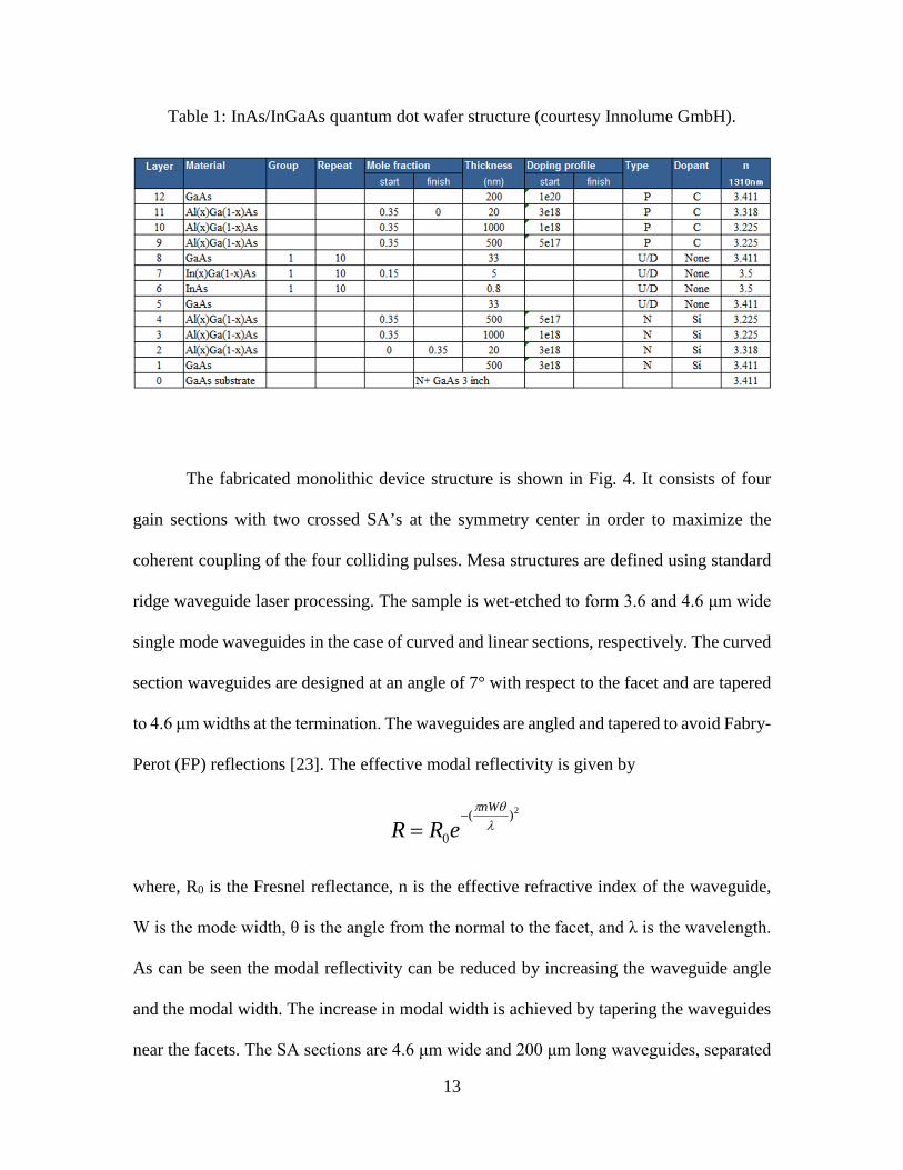
Table 1: InAs/InGaAs quantum dot wafer structure (courtesy Innolume GmbH).
The fabricated monolithic device structure is shown in Fig. 4. It consists of four
gain sections with two crossed SA’s at the symmetry center in order to maximize the
coherent coupling of the four colliding pulses. Mesa structures are defined using standard
ridge waveguide laser processing. The sample is wet-etched to form 3.6 and 4.6 μm wide
single mode waveguides in the case of curved and linear sections, respectively. The curved
section waveguides are designed at an angle of 7° with respect to the facet and are tapered
to 4.6 μm widths at the termination. The waveguides are angled and tapered to avoid Fabry-
Perot (FP) reflections [23]. The effective modal reflectivity is given by
where, R0 is the Fresnel reflectance, n is the effective refractive index of the waveguide,
W is the mode width, θ is the angle from the normal to the facet, and λ is the wavelength.
As can be seen the modal reflectivity can be reduced by increasing the waveguide angle
and the modal width. The increase in modal width is achieved by tapering the waveguides
near the facets. The SA sections are 4.6 μm wide and 200 μm long waveguides, separated
2)(
0λθπnW
eRR−
=
13

by a 15 μm gap from the gain sections. All the gain and SA sections facets are further
angled relative to each other to avoid FP reflections. Benzocyclobutene (BCB) polymer is
used for planarization and standard Ti-Au and Ni-Ge-Au metal contacts are used for the p
and n-side of the wafer after lapping and polishing. All four gain sections are electrically
isolated from each other, allowing for individual control of the DC bias currents to help
achieve optimal mode-locking. No anti-reflection (AR) coatings are used on the cleaved
facets (R ~ 32%). Single mode operation is verified with effective index method and beam
profiling and by efficient coupling to single mode fiber (SMF).
Figure 4: (Left): Fabricated device before metallization with BCB as the isolation
layer (seen in green). (Right): Magnified picture showing crossed saturable
absorbers, each being 200 μm in length.
14

Figure 5: Photomask parameters of the curved two-section device.
Table 2: Photomask parameters for the curved and saturable absorber sections in
the multi-section device.
Ltot Lsa Wsa Lga
L1 L1ta
Wg Le θ L2ta
L2 Wta
[µ
15
20
5 15 30 80 4 0 7° 70 30 5
Figure 6: Photomask parameters of the semiconductor optical amplifier (SOA)
device.
15

Figure 7: Bars of (two not cleaved bars consisting of nine devices each) fabricated
SOAs before cleaving.
The semiconductor optical amplifiers (SOA) used to amplify the output of the
lasers are fabricated using the same QD wafer and consist of 4 μm wide and 3 mm long
ridge waveguide angled at 7° to the facet. The nominal small signal gain of these devices
with and without AR coatings is around 21 dB and 13 dB respectively. The multi-section
device and the SOA’s are mounted p-side up on a copper heat sink and are maintained at
a constant temperature (20° C) using a thermoelectric cooler.
16

2.3.1 Fabrication procedure
1. QD wafer cleaving and degreasing
The wafer is cleaved along the appropriate crystalline axis
And subsequently cleaned with acetone, methanol and iso-propanol
If required the sample is briefly immersed in an ultrasonic bath at low power
2. Photolithography
Spin coat S1805 positive resist
• 3500 rpm for 40 sec
• 500 nm thickness
Pre-bake (120°C for 4 min)
UV exposure (12mW for 5.5 sec)
Develop in 351:DI (10ml:70ml for 35 sec)
Post-bake (120°C for 4 min)
Note: The waveguide is located along major axis [011]. The wet etchant used results in
mesa ridge waveguide structure regardless of the wafer orientation.
Figure 8: Schematic illustrating positive photolithography steps.
17
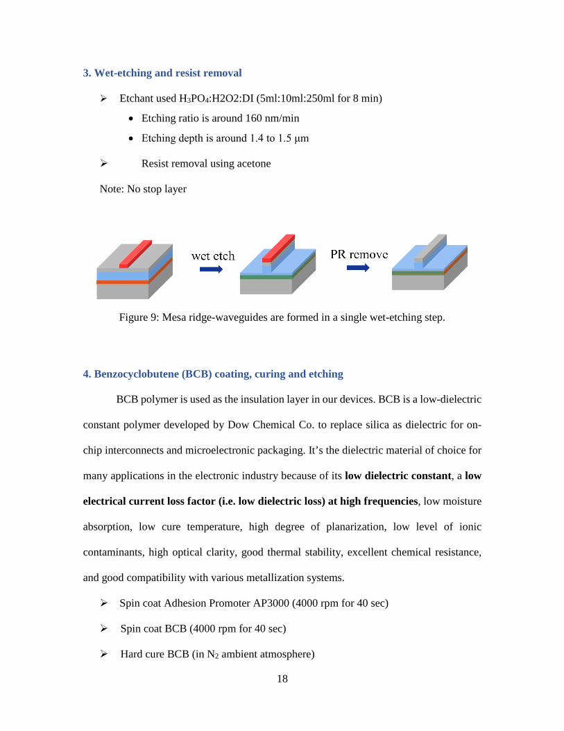
3. Wet-etching and resist removal
Etchant used H3PO4:H2O2:DI (5ml:10ml:250ml for 8 min)
• Etching ratio is around 160 nm/min
• Etching depth is around 1.4 to 1.5 μm
Resist removal using acetone
Note: No stop layer
Figure 9: Mesa ridge-waveguides are formed in a single wet-etching step.
4. Benzocyclobutene (BCB) coating, curing and etching
BCB polymer is used as the insulation layer in our devices. BCB is a low-dielectric
constant polymer developed by Dow Chemical Co. to replace silica as dielectric for on-
chip interconnects and microelectronic packaging. It’s the dielectric material of choice for
many applications in the electronic industry because of its low dielectric constant, a low
electrical current loss factor (i.e. low dielectric loss) at high frequencies, low moisture
absorption, low cure temperature, high degree of planarization, low level of ionic
contaminants, high optical clarity, good thermal stability, excellent chemical resistance,
and good compatibility with various metallization systems.
Spin coat Adhesion Promoter AP3000 (4000 rpm for 40 sec)
Spin coat BCB (4000 rpm for 40 sec)
Hard cure BCB (in N2 ambient atmosphere)
18

Table 3: Hardcure temperature profile.
Step 1 5 min. ramp to 50°C 5 min. soak
Step 2 15 min. ramp to 100°C 15 min. soak
Step 3 15 min. ramp to 150°C 15 min. soak
Step 4 60 min. ramp to 250°C 60 min. soak
Step 5 natural cool down
Dry-etch BCB using RIE
• O2:CF4 (10ccm:5ccm for ~ 9 min)
• Etching ratio is 150nm/min
Soak in Ash Residue Remover (ReziTM-28 for 5 min)
Figure 10: BCB polymer is used as the dielectric insulation layer.
5. Photolithography
Spin coat NR7-1000PY negative resist (4000 rpm for 40 sec)
Pre-bake (150°C for 4 min)
UV exposure (12mW for 14 sec)
Develop in 351:DI (10ml:70ml for 35 sec)
Post-bake (150°C for 4 min)
19

Figure 11: Schematic illustrating negative photolithography steps for depositing p-
side metal contacts.
6. P-side metallization
Ohmic contact is created using Ti and Au followed by high-temperature anneal in
a protective N2 gas ambience.
De-oxidation using H3PO4:DI (6ml:180ml for 5 sec)
Metal deposition, Ti (5nm) and Au (300 nm)
Lift-off using Resist Remover (RR2 for 5 min)
Rapid thermal annealing (RTA = 400°C for 1 min)
Note: It’s a non-alloy ohmic contact (because of high doping density of Carbon in p-
GaAs ~ 1020) where Ti is used as an adhesive layer to promote adhesion of Au to GaAs.
High-temperature annealing improves the contact resistivity (resistivity < 10-6 Ωcm2).
20
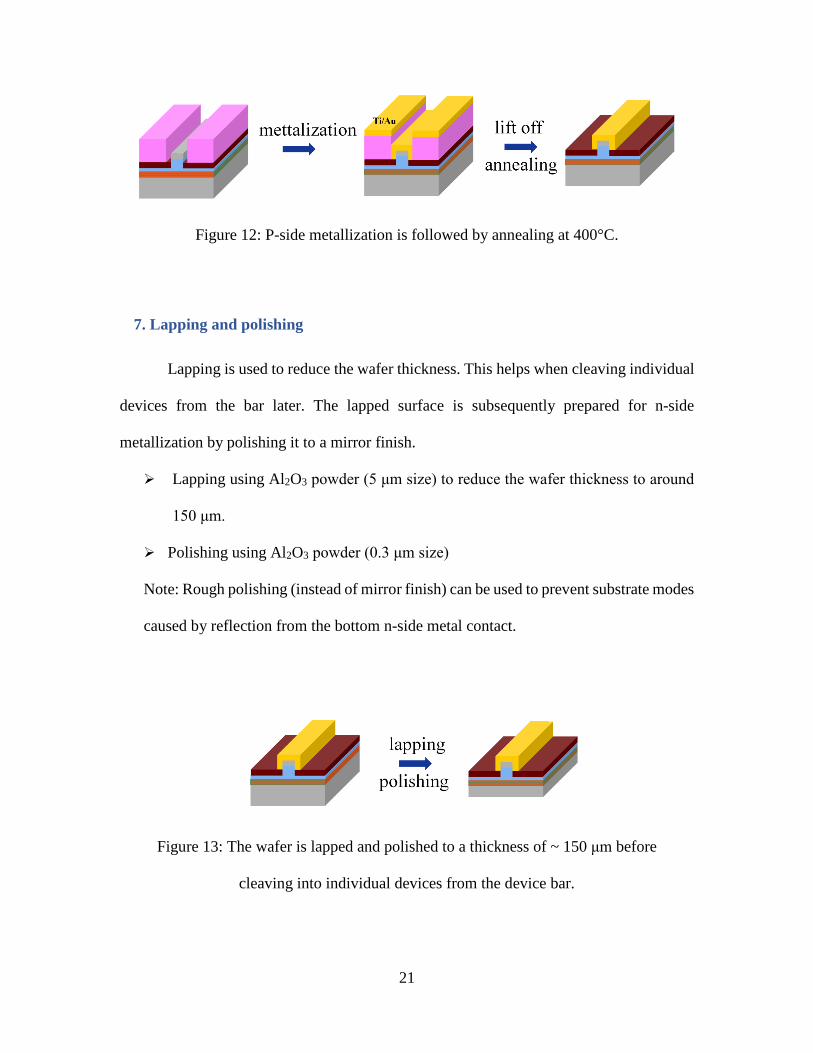
Figure 12: P-side metallization is followed by annealing at 400°C.
7. Lapping and polishing
Lapping is used to reduce the wafer thickness. This helps when cleaving individual
devices from the bar later. The lapped surface is subsequently prepared for n-side
metallization by polishing it to a mirror finish.
Lapping using Al2O3 powder (5 μm size) to reduce the wafer thickness to around
150 μm.
Polishing using Al2O3 powder (0.3 μm size)
Note: Rough polishing (instead of mirror finish) can be used to prevent substrate modes
caused by reflection from the bottom n-side metal contact.
Figure 13: The wafer is lapped and polished to a thickness of ~ 150 μm before
cleaving into individual devices from the device bar.
21

8. N-side metallization, cleaving and mounting
Ohmic contacts are metalized onto the waveguides by thin-film evaporation
whereby, Ni, Ge and Au are deposited using thermal evaporation and the metal film is then
heated (in a protective N2 gas ambience) to the eutectic temperature to alloy the ohmic
metal to the semiconductor.
De-oxidation using H3PO4:DI (6ml:180ml for 5 sec)
Metal deposition, Ni (2nm), Ge (20nm) and Au (200 nm)
Rapid thermal annealing (RTA = 400°C for 1 min)
Note: It’s an alloyed ohmic contact (resistivity better than 10-6 Ωcm2 shown) where Ge
serves as the dopant. Ni has the role of avoiding the balling up of Au-Ge alloy, reduce
the formation of surface oxides and to facilitate the incorporation of Ge dopant.
Figure 14: After n-side metallization and annealing at 400°C, individual devices are
cleaved and mounted on gold-coated copper studs.
22

Figure 15: SEM image of the facet of a fabricated device.
The individual devices are precisely cleaved using a diamond tip mounted on a
three axis translation stage and subsequently soldered on a gold coated copper stud. Au
bonding wire is used to make electrical connections to the cleaved device since Au wire
bonded to Au bonding pad is extremely reliable as the bond is not subjected to interface
corrosion or intermetallic formation.
23

Figure 16: Multi-section device mounted inside the setup. Shown below are SOAs
mounted on gold coated copper studs.
2.3.2 Broadband anti-reflection coatings
Anti-reflection coatings are used on the fabricated quantum dot amplifiers to reduce
the facet reflectivity and improve the overall power output from these devices. The coatings
are fabricated in-house using an e-beam evaporator with an in-situ ellipsometer. The real
time in-situ ellipsometric monitoring is useful for control of the coating process and offers
better accuracy and reliability than crystal monitors, especially for sub 100 nm optical
24

thickness. Considering the broad gain bandwidth (>100nm) of the quantum dot SOA’s a
three layer W-coat design is used. The three layer structure achromatizes the design over a
broad bandwidth. The three materials used in our coating are Al2O3, Si and SiO2 and the
optical thicknesses used are optimized over the highest bandwidth possible (with low
reflectivity) using “Essential Macleod” thin film software.
Table 4: Anti-reflection coating parameters (reference wavelength λ = 1310 nm).
Layer n t (nm)
Air 1.000
SiO2 1.438 241
Si 3.507 34
Al2O3 1.800 48
Substrate 3.408
25

Figure 17: Reflectance diagram (for s-polarization).
26
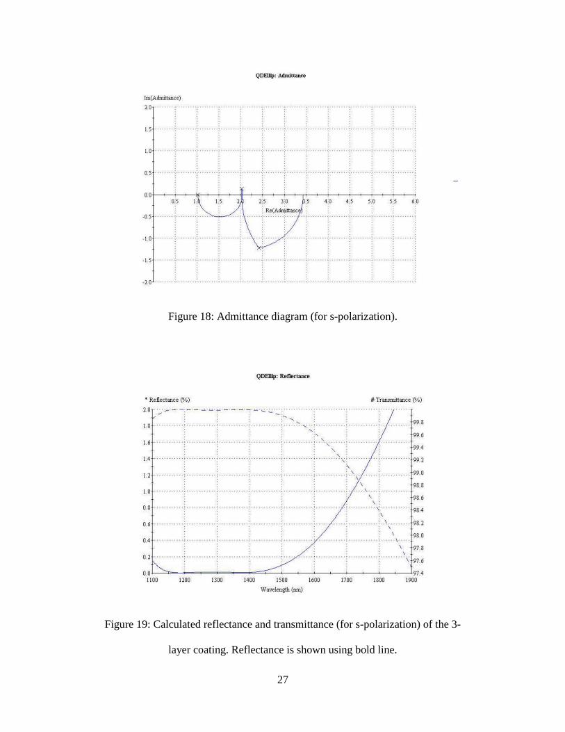
Figure 18: Admittance diagram (for s-polarization).
Figure 19: Calculated reflectance and transmittance (for s-polarization) of the 3-
layer coating. Reflectance is shown using bold line.
27

Figure 20: Calculated reflectance as a function of incident angle.
Initial measurements of the reflectivity of the three layer coating was done by
coating a linear 1.5 mm long monolithic fabry-perot quantum dot laser (λc = 1270 nm) with
cleaved facets (R~30%). Kaminow-Eisenstein method, which is based on Hakki-Paoli, is
used for the determination of the reflectivity of the coated device [24]. The device is
mounted and operated just below threshold current and the modulation of intensity
measured using an optical spectrum analyzer. The depth of modulation is given by
, with ;
minmax
minmax
PPPP
m+−
= 212
aa
m+
= LL RaR 2* =
28

Here “a” is the amplification factor. The reflectivity RL* of the coated facet is then
calculated using the known cleaved facet reflectivity RL = 0.3. The measured modulation
intensity and the calculated reflectance for the fabry-perot device are shown in Fig. 22. As
seen, even at high pumping currents no lasing is observed. The coatings when fabricated
on the 3 mm long quantum dot amplifiers resulted in an improvement in the resultant gain
from these devices which improved from ~ 12 dB to more than 19 dB (with SOA biased at
I = 300 mA).
Figure 21: LI-IV curves of the 1.5 mm Fabry-perot laser before and after AR
coating.
29

Figure 22: Measured reflectivity of the coated fabry-perot laser (λc = 1270 nm)
using Kaminow-Eisenstein method. Also shown is the optical spectrum with no
lasing seen even at higher injection currents.
30

Figure 23: Delrim fixture with a bar of SOAs for AR coating
Figure 24: Graph showing the gain comparison of the coated and uncoated SOAs.
31

2.4 Experimental setup
Fig. 25 illustrates the experimental setup. The monolithic CPM cavity formed by
the cleaved facets has a total length of about 2.8 mm. However because of the two counter
propagating pulses traveling simultaneously in the cavity, the fundamental repetition rate
in the CPM configuration is twice the free spectral range of the whole cavity. The CPM
resonant cavity thus has a repetition rate of 29.46 GHz. For the master oscillator, the two
curved sections serve as the gain medium. As seen in the figure, the cavity is built with
four gold coated external mirrors, with two mirrors mounted on a translation stage to
control and precisely match the cavity length to a sub-harmonic of the CPM laser. The
chosen cavity length corresponds to a free spectral range (FSR) of 446 MHz which is the
66th sub-harmonic of the CPM laser. In the operation mode, all the gain sections are driven
by constant-current sources, while a voltage source provides the reverse bias to the
absorber sections.
32

Figure 25: Schematic drawing of the experimental setup. SOA, semiconductor
optical amplifier; BS, pellicle beam splitter (92-8%); λ/2, half-wave plate; ISO,
optical isolator; OSA, optical spectrum analyzer.
It should be noted that because of the common SA region, the reverse bias voltage
and the bias currents used in the experiment are carefully chosen to achieve simultaneous
stable mode-locking of the external cavity and the CPM laser and to achieve optical
spectral overlap of the two cavities. The spectral overlap induces coupling between the two
cavities whereby the injected pulses transfer the phase stability to the longitudinal modes
of the CPM slave laser, thus injection locking the CPM laser to the master laser.
33

2.5 Measurement and results
To begin, the external ring cavity is first aligned to operate in a continuous wave
(CW) regime by applying forward bias current of 70 mA on each of the two curved gain
sections, using separate DC probes and current sources. The threshold current of the laser
is ~ 35 mA (applied on each gain section with no voltage on the absorber section). Two
aspheric lenses are used to collect and collimate the light inside the ring cavity. Passive
mode-locking is achieved by applying reverse bias voltage of -6.5 V to the crossed SA
section, which is kept constant through all measurements. The light is coupled out of the
ring cavity using a pellicle beamsplitter with small reflectance (8%) to minimize the cavity
losses. The output is amplified using an SOA and then coupled to single mode fiber for
diagnostics. A free space optical isolator is used to avoid coupling of the SOA emission
back into the master oscillator and a half-wave plate serves to match the TE polarization
of the SOA. The spectral and autocorrelation measurements are shown in Fig. 26. The 3
dB spectral width is 3.6 nm. The pulse width is estimated to be 5.21 ps, assuming a
Gaussian pulse shape. The time-bandwidth product (TBP) is thus 3.29, which is 7.5 times
transform limit.
34

Figure 26: Spectra of the passively mode-locked high-Q external cavity (master)
laser: (a) Optical spectrum, (b) RF power spectrum showing 66th harmonic, (c)
Autocorrelation trace, (d) Optical linewidth, measured using the self-heterodyne
setup.
The optical linewidth in Fig. 26 (d), is measured using the delayed self-heterodyne
technique [25]. The schematic of the setup is shown in Fig. 27. The laser output is amplified
using a fiberized amplifier before the Mach-Zehnder interferometer. A free space acousto-
optic modulator operating at 100 MHz in one of the arms together with 200 meters fiber
delay in the other produces an uncorrelated beat tone at 100 MHz on the electrical spectrum
analyzer which gives us the measure of the average optical linewidth, as it’s the result of a
heterodyne beat of two combs. Derickson outlines a comprehensive method for
35

determining the linewidth of a laser following Lorentzian linewidth statistics [25]. Since
semiconductor laser linewidths are dominated by frequency jitter, or 1/f noise, linewidths
are measured more accurately by determining the width at levels further down from the
peak than the half-maximum. Since a delayed self-heterodyne beat result in a convolution
of Lorentzian curves, a deconvolution factor is necessary. For the 10 dB width, this factor
is 2√9 Δν. The measured 10 dB average optical linewidth of the master laser is ~ 18 MHz
which thus yields a laser linewidth of Δν = 3 MHz, after deconvolution.
Figure 27: Schematic drawing of the delayed self-heterodyne setup used to measure
the optical linewidth of both lasers. SOA, semiconductor optical amplifier; AOM,
acousto-optic modulator; PC, polarization controller; PD, photodetector.
36

The slave CPM laser is passively mode-locked at the fundamental repetition rate of
29.46 GHz by applying a forward bias current of 28 mA on each of its linear gain sections.
The reverse bias voltage is -6.5 V which, as mentioned, is shared and kept constant with
the SA of the master oscillator. The threshold current of the laser is ~ 20 mA (applied on
each gain section with no voltage on the absorber section). Light is coupled out using an
aspheric lens and then amplified using an SOA before going to the diagnostic equipment.
As seen in Fig. 28(a), the laser exhibits supermode noise (a characteristic of harmonic
mode-locking) with the optical spectrum showing two sets of optical modes spaced at the
cavity FSR. The measurements before injection are taken by physically blocking the light
inside the master ring cavity. Optical pulse injection is achieved by removing this beam
block. As seen in Fig. 28, supermode suppression in the optical domain is not only
accompanied by RF linewidth reduction but also by reduction in the average optical
linewidth after injection locking. There is a more than 10 dB reduction in the RF noise
level at 20 MHz offset from the carrier. The RF tone width is reduced from 24.35 MHz to
4.88 MHz measured 30 dB down from the carrier, which is an almost 5-times reduction.
This is accompanied by a reduction of the 10 dB average optical linewidth, from 46 MHz
to 18 MHz. After deconvolution, this corresponds to a laser linewidth reduction from ~ 8
MHz to 3 MHz after injection locking. The intensity autocorrelation measurements are
shown in Fig. 28 (d). The pulse width is estimated to be 4.32 ps, assuming a Gaussian pulse
shape. The 3 dB spectral width is 1 nm. The TBP is thus 0.757, which is 1.72 times
transform limit. The autocorrelation trace (and hence the pulse width) remains unaffected
by injection locking.
37

Figure 28: Spectra of the passively mode-locked CPM (slave) laser before (in blue)
and after (in red) optical injection: (a) Optical spectrum before injection, (b)
Optical spectrum after injection, (c) Comparison of RF power spectrum showing
almost 5-times reduction in the 30 dB RF linewidth after injection, (d)
Autocorrelation trace, remains indistinguishable after injection locking (e) Optical
linewidth before injection, (f) Optical linewidth after injection showing close to 3-
times reduction in the 10 dB optical linewidth.
38

The mechanism of stabilization can be explained as due to the optical pulse
injection from the master laser into the CPM cavity, which injection locks the CPM laser
to the stable master oscillator. Injection locking is confirmed by the supermode suppression
and the reduction in the optical linewidth of the CPM laser, which is seen to closely match
the linewidth of the master. The adjustment of the optical pulse timing of the CPM laser
by the pulses of the master oscillator further leads to the sharpening in the RF spectrum
peak and hence the RF linewidth reduction. However, the pulse width of the CPM laser
remains the same after injection locking, indicating that the main pulse-formation
mechanisms such as saturable absorption and saturable amplification are still dominated
by the slave laser. Because the four pulse interaction is only occurring periodically (every
66th pulse of the slave laser), pulse shortening does not occur as might be expected with
higher optical intensity in the SA. As mentioned earlier, the injection locking occurs
because of the transient grating formation at 45° to the face of the SA which is responsible
for the interaction between cavities. Since the diffraction efficiency from the transient
gratings induced by the pulse overlap is estimated to be ~ 10-3, which is orders of magnitude
larger than any other linear scattering effect such as diffractive signal leakage, this indicates
that the injection locking mechanism is predominantly due to four-wave mixing.
39
CHAPTER 3 CONFIRM FOUR-WAVE MIXING PROCESS AS THE PRIMARY
INJECTION LOCKING MECHANISM
In this chapter we describe an experiment to confirm FWM process as the primary
mechanism responsible for the observed injection locking in the novel design. This is the
first time, to the best of our knowledge that FWM has been conclusively shown to be used
for injection locking in semiconductor media especially in an orthogonal waveguide
configuration. We also subsequently investigate the contributions from other mechanisms
such as linear scattering which are found to be negligible as expected in the case of low-
index contrast perpendicular waveguide crossings [26], [27].
40

3.1 Experimental setup
Fig. 29 illustrates the experimental schematic. Under normal operating conditions,
both lasers operate bidirectionally i.e., both lasers are operating in the CPM regime.
However, in order for the FWM effect to be unambiguously identified, a free space
circulator is added to force unidirectional operation of the ring laser and allow access to
the ASE output in backwards direction from the other facet (port-2) of the ring laser. This
counter-clockwise ASE output is analyzed before and after injection to confirm the FWM
process.
The devices used in the experiment are the same as described previously. The monolithic
CPM cavity is cleaved at a length of 2.8 mm and is passively mode-locked by applying a
negative bias voltage to the SA section. With a forward bias current of ~ 25 mA on each
of the linear gain section and a reverse bias voltage of -6.1 V ± 0.1 V on the SA, the laser
typically emits close to transform limited pulses of some few picoseconds. It should be
noted that because of two counter-propagating pulses traveling simultaneously in the cavity,
the repetition rate in the CPM configuration is twice the free spectral range (FSR) of the
whole cavity. The monolithic CPM cavity thus has a pulse repetition rate of ~ 29.44 GHz.
41

Figure 29: Schematic of the experimental setup to confirm four-wave mixing
(FWM). The horizontal and vertical polarized light is shown using symbols H and
V, respectively. The symbol Hb and Vb denote the polarization of the backward
emitted ASE light in the counter-clockwise direction. The output ports of the
external ring laser are marked as 1 and 2, respectively. ASE, amplified spontaneous
emission; SOA, semiconductor optical amplifier; Pol, linear polarizer; PBS,
polarizing beam splitter; FR, faraday rotator; BS, pellicle beam splitter; λ/2, half-
wave plate; ISO, optical isolator.
42

The external high-Q ring laser is built using four gold coated external mirrors, with
two mirrors mounted on a translation stage to control and precisely match the cavity length
to a sub-harmonic of the CPM laser. The chosen cavity length corresponds to an FSR of
446 MHz, which is the 66th sub-harmonic of the CPM laser. A free space optical circulator
is build inside the cavity with the help of a polarizing beam splitter (PBS), faraday rotator
(FR) and a half-wave plate. This allows the cavity to operate unidirectional (clockwise)
while simultaneously giving access to the ASE output emitted from the other facet in the
counter-clockwise direction. Because of the non-reciprocity of the FR, this ASE
component is vertically polarized and thus coupled out using the same PBS for analysis.
Note that the light emitted from the semiconductor diode laser is horizontally polarized
(TE) to begin with and care is taken to maintain that polarization by placing linear
polarizer’s at the outputs of the laser, which eliminates any residual vertical polarized light
component arising from the minute tilt of the device while mounting. Passive mode-locking
is achieved by applying a reverse bias voltage of -6.1 V on the common SA region, which
is shared and kept constant with the SA of the CPM laser. The corresponding forward bias
current used is 80 mA on each of the curved gain sections giving a pulsewidth of around 5
ps. As before, the reverse bias voltage and bias currents used in the experiment are carefully
chosen to achieve simultaneous stable mode-locking of the external cavity laser and the
CPM laser and to achieve optical spectral overlap of the two cavities.
3.2 Measurement and results
Injection locking is first verified by examining the RF and optical spectra of the
CPM laser for reduction in the RF linewidth and for optical supermode suppression. As
seen in Fig. 30(d), the reduction is not as drastic as observed previously, because of the
43

three-pulse interaction in the current setup as opposed to four pulses, though it’s sufficient
to achieve FWM and injection lock the CPM laser. The measurements before injection are
taken by physically blocking the light inside the master ring cavity. Optical pulse injection
is achieved by removing this beam block.
Figure 30: (a), (b): Typical spectra of the passively mode-locked high-Q external
cavity (master) laser. (c), (d): Typical spectra of the passively mode-locked CPM
(slave) laser before (in blue) and after (in red) optical injection.
44

Fig. 31(a) shows the optical spectrum of the backward propagating ASE output
from port-2 of the external ring laser before and after injection. As seen in the figure,
because of the back reflections from the circulator optics inside the external ring cavity,
we do get leakage of the ring cavity lasing spectrum coupled to the ASE output, which
though small can affect our measurements. The presence of the CPM light is then
highlighted by examining the background subtracted ASE before and after injection
locking. This is obtained by subtracting the two measured spectra shown in Fig. 31(a)
displaying the result in Fig. 31(b). In the resultant difference spectra, the center of the
spectrum clearly shows the diffracted spectra of the CPM laser which matches the location
where the CPM mode-locked peak otherwise would fall.
45

Figure 31: (a): Backward propagating ASE spectra from port-2 of the passively
mode-locked high-Q external cavity (master) laser with and without injection of the
CPM laser. Also seen is the back reflected leakage light from the intra-cavity optics
superimposed on the ASE spectra. (b): Background subtracted spectra from Fig.
31(a), showing the diffracted CPM spectra present in port-2 due to FWM. (c): ASE
spectra from port-2 of the master laser with port-1 physically blocked. (d):
Background subtracted spectra from Fig. 31(c), with no residual CPM laser light
observed in the absence of FWM.
46

It should be noted that the normal output of the 29.44 GHz CPM laser shows an
axial mode spacing of 29.44 GHz. This is because there are two coherent pulse trains
oscillating in a 14.72 GHz cavity, but temporally delayed by half-round trip. The resulting
output thus displays an axial mode spacing of 29.44 GHz due to the spectral interference
and resulting spectral modulation caused by the temporal delay of the two-pulse trains of
~ 34 ps. On the other hand, the output spectrum of the FWM signal shows an axial mode
spacing of 14.72 GHz. This is because the two coherent pulse trains that possess axial
modes at 14.72 GHz are diffracted simultaneously i.e., both pulse trains are temporally
overlapped in time, resulting in observed spectra with axial modes at 14.72 GHz. Finally,
it should be noted that the diffracted pulse occurs only every ~ 2 ns. This produces an
additional spectral substructure at 446 MHz which is not spectrally resolved.
To make sure that the observed CPM light superimposed on top of the ASE output
is only due to the aforementioned FWM and not due to any other linear scattering effect,
we also measure the same ASE output from the ring cavity laser with and without CPM
lasing while physically blocking port-1 before the PBS and keeping all the bias conditions
the same. Any leakage of the CPM light into the ring cavity would then be seen in the
measured optical spectrum. However, as seen in Fig. 31(d), the resultant subtracted
spectrum with and without the port-1 blocked shows no residual CPM light, confirming
that FWM is the primary mechanism for the injection locking in our design.
47

CHAPTER 4 IMPROVED STABILIZATION ARCHITECTURE
With an all passive stabilization architecture, the four-wave mixing technique is
already shown to be very effective in reducing the long term frequency drift as well as the
timing jitter of the high-repetition rate CPM laser. A QD based mode-locked design further
offers reduced spontaneous emission rate and low threshold current density which leads to
reduced noise. The extent of stabilization is, however, limited by the frequency and phase
stability of the master ring laser which is passively mode- locked and thus still suffers from
excess noise arising from the pulse-to-pulse timing fluctuations in the absence of any
external synchronization [6], [7]. The optical phase noise and the timing jitter manifests
themselves as the wide optical and RF linewidths of the master laser. In this chapter, we
report on the performance of one scheme to overcome this limitation and help improve the
design with jitter values that are more suitable and required for use in the future coherent
communication systems.
48

4.1 Experimental setup
Fig. 32 illustrates the principle of the proposed scheme. The multi-section device
consists of four gain sections and has a crossed saturable absorber (SA) section located at
the symmetry center of the device. The monolithic CPM laser is formed from the cleaved
facets of the linear gain sections. The two curved gain sections are part of an external high-
Q ring cavity which is precisely built to a length corresponding to a subharmonic of the
CPM slave laser. A fiberized lithium niobate (LibNO3) intensity modulator is introduced
to hybridly mode-lock and hence improve the phase stability of the master laser. The
electro-optic modulator facilitates an all optical modulation, thus avoiding any electrical
cross talk between gain sections which is otherwise seen when applying an RF modulation
instead. By employing a longer cavity (compared to our previous work) and by using anti-
reflection (AR) coatings on the curved gain facets further helps to improve the Q of the
ring cavity which translates into an improved RF and optical stability of master laser. This
improved stability is transferred to the monolithic CPM laser when the four pulses from
the two crossed laser cavities meet in the common SA region. The pulse overlap leading to
the formation of transient gratings (referred to degenerated FWM) with a resulting index
of refraction at 45º to the face of the SA which causes the pulses to diffract from individual
cavities into each other, essentially locking the CPM laser to the ring laser [17]. The
principle of the method is confirmed by observing the narrowing of the RF and optical
linewidths of the CPM laser giving rise to a stable ~ 30 GHz optical pulse train with pure
spectral properties.
49

Figure 32: A schematic of the experimental setup. CPM: colliding pulse mode-
locked slave laser, λ/2: half-wave plate, BS: beam splitter.
The monolithic gain chip is fabricated using the same commercially available
quantum dot epi-wafer as described in chapter 2 and has the same waveguide design
specifications. The gain chip is mounted on a gold coated copper stud and shares a thermo-
electric (TEC) cooler with the external ring cavity for temperature control. The monolithic
CPM slave laser has a total length of about 2.8 mm and under proper biasing conditions
has two counter-propagating pulses which collide directly in the SA. As expected, this
leads to a repetition rate of ~ 29.4 GHz which is twice the free spectral range (FSR) of the
monolithic cavity. The master ring laser, with the two curved gain sections, is built using
two external mirrors and a commercial mach-zehnder based fiberized LiNbO3 intensity
modulator. Aspheric lenses couple the light output from the facets into the lens collimators
of the pigtailed LiNbO3 modulator. The lens collimators are mounted on x, y, z stages to
50

control and precisely match the cavity length to a subharmonic of the CPM laser. Care is
taken to match the left and right arms of the cavity for the pulses to meet inside the LiNbO3
modulator in the bi-directional cavity. The chosen free-space length of the ring cavity is ~
1.57 m, which corresponds to an FSR of 191 MHz. Half-wave plates inside the ring serve
to match the polarization state of the LiNbO3 modulator for maximum extinction and
dominantly couple the TE mode back to the gain chip (since the QD laser lases in TE mode).
In operation mode, all the gain sections are driven by constant current sources, while a
voltage supply provides the reverse bias to the absorber section. Because of the common
SA region, the reverse bias voltage and the bias currents used in the experiment are
carefully chosen to achieve simultaneous stable mode-locking of the external cavity and
the CPM laser. The output from the lasers is amplified using semiconductor optical
amplifier (SOA), coupled into an SMF fiber, and finally split into a various number of
instruments for diagnostics. The optical linewidths of the lasers are measured using the
delayed self-heterodyne setup shown in Fig. 33.
Figure 33: Delayed self-heterodyne setup used for optical linewidth measurement
with 1-km of optical fiber.
51

The laser output is amplified using an SOA before going into an Mach-Zehnder
interferometer (MZI). A splitting ratio of 80/20 is used to take care of the free-space to
fiber coupling loss in case of the free space acousto-optic modulator (AOM) placed in one
of the arms of the interferometer, operating at 100 MHz. The other port of the MZI is
delayed by 1.0 km optical fiber which produces a uncorrelated beat tone at 100 MHz on an
electrical spectrum analyzer and gives us a measure of the optical linewidth.
4.2 Measurement and results
Continuous wave (CW) operation of the high-Q ring laser is first confirmed by
applying forward bias currents on each of the two curved gain sections, using DC probes.
The QD based laser emits at 1.3 µm and has a threshold current of ~ 47 mA (applied on
each gain section with no voltage on the absorber section and with LiNbO3 modulator at
transparency). Fundamental passive mode-locking at 191 MHz is observed with a reverse
bias voltage of – 3.0 V ± 0.1 V on the SA. Because of the common crossed SA section, a
SA voltage of -6.0 V (with a corresponding bias current of 100mA on each of the gain
sections) is chosen, which gives a stable third harmonic mode-locking of the laser at 573.45
MHz and also results in a simultaneous stable mode-locking of the CPM laser. Hybrid
mode-locking is achieved by applying an RF power of 20.5 dBm to the LiNbO3 intensity
modulator (from a sin-wave source at 573.45 MHz) and results in a much reduced phase
noise compared to just passive mode-lock operation. The light is coupled out of the ring
cavity using a pellicle beam splitter with a small reflectance (8%) to minimize the cavity
loses and then amplified before photo-detection.
The spectral and the time domain outputs are shown in Fig. 34. A 50-GHz sampling
scope triggered by the external microwave source clearly displays stable pulse train at the
52

laser frequency of 573.45 MHz, confirming that the third-order subharmonic hybrid mode-
locking is indeed taking place synchronized to the microwave source. Also shown is the
10 dB optical linewidth of the ring laser. Since it is the result of a heterodyne beat of two
combs, an average optical linewidth of ~3.74 MHz is measured. Taking into account the
deconvolution factor of 2√9 Δν for the 10 dB Lorentzian linewidth, yields a master laser
linewidth of Δν = 623 KHz.
Figure 34: Spectra of the hybridly mode-locked (3rd harmonic mode-locking) high-
Q external cavity (master) laser.
53

The CPM QD laser is passively mode-locked at the fundamental repetition rate of
29.4 GHz by applying a forward bias current of 46 mA on each of its gain sections and a
reverse bias voltage of –6.0 V ± 0.1 V on the SA section. The threshold current of the laser
is ~ 34 mA (applied on each of the linear gain sections with no voltage on the absorber
section). Light is coupled out using an aspheric lens and then amplified using an SOA
before going for diagnostics. The device temperature is tuned to ~ 19º C, to achieve optical
spectral overlap of the two cavities which induces coupling and hence injection locking of
the CPM laser to the high-Q external cavity. As seen in Fig. 36, the optical linewidth of
the master ring laser does suffer when the bias conditions and temperature is tuned to
achieve the optical spectral overlap with the CPM laser. In the near future, this can be easily
circumvented by employing individual on-chip tuning elements such as heaters and Bragg
gratings for the two lasers.
Figure 35: Optical spectral overlap of the slave and master laser achieved by tuning
the device temperature (~18 º to 19 º C).
54

Figure 36: Optical linewidth variation of master ring-cavity with bias-conditions
and temperature.
Fig. 37 (a)-(d) shows the optical and RF spectra of the passively mode-locked CPM
laser before and after optical injection. As seen in Fig. 37(a), the CPM laser simultaneously
operates with two sets of axial modes, (a characteristic of harmonic mode-locking) with an
optical spectrum where the axial modes are spaced at the cavity FSR. In Fig. 37(b), the
optical spectrum of the CPM laser is shown after injection locking. The previously
observed, free running, passive mode- locked spectra, is now transformed to a spectra
55

showing an axial mode spacing of 29.4 GHz, which is a result of the injection process
establishing coherency between the oscillating pulse pairs in the CPM lasers. The resulting
coherence between the oscillating pulse pairs mandates that the axial modes of the injection
locked CPM laser be observed at 29.4 GHz.
Fig. 37(c) shows the RF power spectra of the photodetected pulse train from the
CPM laser, before and after injection locking. It is evident that the fundamental mode-
locked frequency of the CPM laser has been pulled to the harmonic beat frequency of the
injected master ring laser and the linewidth and the frequency fluctuation of the detected
mm-wave carrier are drastically reduced. It should be noted that the RF linewidth is
reduced from 4.64 MHz to 332 KHz, as measured 10 dB down from the carrier. This
reduction in the RF linewidth is attributed to the injection locking process, which assists in
establishing a well-defined phase relationship among the different axial modes in the
optical domain, and is clearly evident, as manifested by more than 14-times reduction in
the RF linewidth of the CPM laser. In addition, in Fig. 37(d), it is observed that the optical
linewidth sees a ~ 5x reduction in the linewidth, from 5.40 MHz to 1.13 MHz (10 dB width,
deconvolved) after injection locking. The reduction in the optical linewidth is a direct result
of the CPM laser oscillation being injection locked by FWM and stabilized by the narrow
axial modes from the master, hybridly mode-locked laser.
56

Figure 37: Spectra of the passively mode-locked CPM (slave) laser before (in blue)
and after (in red) optical injection via four-wave mixing.
57

Figure 38: Autocorrelation trace and the measured pulse-width of the CPM laser.
The pulse width of the CPM laser is measured using an intensity auto-correlator.
Assuming a Gaussian pulse shape, the autocorrelation trace shown in Fig. 38 translates into
a pulse width of 4.47 ps and is identical both with and without injection. The optical
spectrum of the pulse has a FWHM of 0.65 nm at wavelength of 1306 nm. The time
bandwidth product (TBP) is thus 0.511, which is 1.16 times the transform limit, indicating
near transform-limited pulses directly from the monolithic CPM laser.
58

CHAPTER 5 FUTURE ALL MONOLITHIC DESIGN
Compared to bulk and fiber optic systems, a photonic integrated device design can
offer improved performance and stability in a smaller footprint and at a lower cost.
Research in recent years has successfully explored various silica-on-silicon and hybrid-
silicon based architectures for ultralow-loss, high-density multilayer waveguide routing for
macro-chip interconnects [28-32]. The emerging research has demonstrated its potential
utilizing low cost, mature and mass productive CMOS processes and the ability to combine
III-V materials with silicon through heterogeneous integration. The limited performance
of passive silicon components (in terms of insertion loss and channel cross talk due to high-
index contrast) has been overcome with the advent of low-loss Si3N4 waveguides offering
propagation loss of less than 0.1dB/m [33].
In this section, we present a unique platform that combines III-V and silicon
photonic components with ultralow-loss Si3N4 waveguides for all-monolithic integration
of the novel four-wave mixing stabilized ultrafast optical pulse. The design can be realized
using an on-chip electro-absorption (EA) modulator or by RF modulating the gain medium
itself at a sub-harmonic of the monolithic CPM laser for achieving a stable optical pulse
source. We illustrate both these designs with detailed schematics and corresponding
reference work.
59

5.1 Using optical hybrid mode-locking
Since silicon is an indirect band gap material, integration of III-V gain media and
silicon is explored. As shown by Mizrahi et al. at Skorpios Technologies [34], the QD gain
media in our case can be embedded within a silicon on insulator (SOI) wafer, where the
epitaxial QD material is metal-bonded directly onto the silicon substrate within a pit
receptor site inside the SOI wafer. The metal bond would serve as the bottom electrical
contact and would avoid the lattice mismatch issues of depositing III-V on silicon. An
illustration of this method together with the device layout is shown in Fig. 39. The gap
which is formed between the gain medium and the silicon can be reconstructed with a
buried oxide layer or Si3N4. As seen in Fig. 39 and Fig. 40, an amorphous silicon or low-
loss Si3N4 waveguide with identical cross-section to those in QD gain media would serve
as an integrated coupler. The integrated coupler forms the connection between the III-V
waveguides and the long Si3N4 waveguides of the high-Q cavity formed on SOI chip. The
gain waveguides are angled as our previous design to suppress unwanted reflections within
the cavity. All waveguide structures can be defined in a single photolithography step
followed by etching, as demonstrated in [34]. For hybrid mode-locking the high-Q ring
cavity, several modulator structures such as micro-ring modulators, electroabsorption
modulators (EAM) and Mach-Zehnder modulators in hybrid silicon have been explored.
Referring to table 5, (from ref. [35]) and looking at some of the listed parameters for each
specific modulator, we feel an EAM modulator which avoids the sensitivity to temperature
and fabrication variations of ring modulators and is compact compared to an MZI
modulator would be an ideal choice for hybrid mode-locking the high-Q ring cavity in the
60

monolithic design. The low-loss EAM modulator on the hybrid silicon platform has already
been demonstrated and can be realized as described in ref. [36].
Figure 39: Illustration of all monolithically integrated novel design with epitaxial
III-V gain material metal-bonded within SOI platform. The design would
incorporate low-loss Si3N4 waveguides in the case of high-Q ring cavity which is
then modulated with EA modulator (III-V based) for low-noise hybrid mode-
locking.
61

Figure 40: Cross-section view of the geometry of the future all monolithically
integrated design.
Table 5: Comparison of silicon modulators (ref. [35]).
62

5.2 Using RF hybrid mode-locking
Another way of realizing the all-monolithic optical pulse source on hybrid silicon
platform is shown in Fig. 41. Instead of having the high-Q cavity in a ring format it can be
also be built from linear Si3N4 waveguides (the waveguides can also be looped into a spiral
if need be) with cleaved AR coated facets or by incorporating distributed Bragg reflector
gratings together with heating elements at the end of the low-loss waveguides. This would
provide an additional benefit whereby the external cavity can be tuned to match the lasing
peak and longitudinal modes of the CPM laser for an optimal injection locking. This
wavelength tuning with fabricated Bragg reflector gratings and heaters has already been
demonstrated in ref. [34], [37]. The design can be further simplified by directly modulating
the gain medium of the high-Q ring laser [38], [39] (with proper RF shielding) and thus
avoiding the requirement of an additional EAM modulator.
Figure 41: Cross-section view of the monolithic device with linear Si3N4
waveguides for the high-Q cavity and tunable distributed Bragg reflector (DBR)
mirrors. The heaters together with DBR mirrors would serve as the phase tuning
element for longitudinal optical mode overlap of the two crossed laser cavities for
optimal injection locking.
63

CHAPTER 6 CONCLUSION
In summary, we have proposed and demonstrated a novel method of stabilizing
high-repetition rate monolithic mode-locked diode lasers by purely optical means. As a
first demonstration, an external high-Q master laser is used to injection lock an
orthogonally coupled passively mode-locked monolithic CPM slave laser. Coupling
between the crossed orthogonal laser cavities is achieved through four-wave mixing in the
common monolithically integrated saturable absorber, which results in the locking and
hence reduction of the timing jitter as well as the long-term frequency drift of the slave
laser. In the initial all passive stabilization architecture, with both master and slave lasers
passively mode-locked, a stable 30 GHz optical pulse train is generated with more than 10
dB reduction in the RF noise level at 20 MHz offset. The RF tone width is reduced by
almost 5-times (from 24.35 MHz to 4.88 MHz) measured 30 dB down from the carrier and
close to 3-times reduction of the 10 dB average optical linewidth (from 8 MHz to 3 MHz)
is observed. Four-wave mixing process is subsequently investigated and experimentally
confirmed to be the primary mechanism responsible for the interaction and locking of the
CPM laser. Other linear scattering effects, which are predicted to be small are also
investigated and found be negligible. The stabilization architecture of the novel coupled
cavity laser is further improved by employing optical hybrid mode-locking and increasing
the Q of the master laser cavity (using a longer cavity and AR coating the laser facets),
which results in dramatic reduction in the optical and RF linewidths of the master ring laser.
This higher stability translates into more than 14-times reduction (from 4.64 MHz to 332
KHz) in the 10dB RF linewidth and almost 5-times reduction in the 10dB optical linewidth
64

(from 5.40 MHz to 1.13 MHz) of the injection locked slave laser, confirming the
effectiveness of the novel technique for all-on-chip stability transfer.
With the novel techniques recently demonstrated, such as active-passive waveguide
integration and long low-loss passive waveguides (in III-V/Silicon), in the near future the
narrow linewidth CPM laser employing the new FWM technique can be fabricated with
the high-Q cavity in an all-monolithic architecture. With the resulting stabilized pulse train,
this ultra-compact and ultrashort optical source would be attractive for use in the
forthcoming photonic access networks employing technologies such as dense wavelength-
division multiplexing (DWDM) and ultra-high speed time division multiplexing (OTDM).
65

APPENDIX A C++ CODE USED FOR MASK LAYOUT
66

define waveguide {
#include "ldata.h" #include <stdlib.h> #include <math.h>
void WaveguideMacro ( void )
{ LPoint Polygon [ 100 ];
/*****General_Variables along x,y*****/
double X,Y,XE;
double Ltot, Wtot, Width, Lsa, Wsa, Lgap, Gap_Cen, Gap_Angle,Gap_Angle1,
L1, L1tap, Le, Lcur, L2, L2tap, Wtap; /***Wtap is Width after tapered***/
/*****Start_Points(0,y)****/
double y_start;
/*****Torus_Variables******/
double x_Torus, y_Torus, R, R_In, R_Out,Torus_Angle,Start_Angle, Stop_Angle,
delta_x, delta_y, R2, R2_In, R2_Out, R5, R5_In, R5_Out;
/*****"Taper+L1" Variables******/
double Rotate,
x0,y0,x1,x2,x3,x4,x5,x6,y1,y2,y3,y4,y5,y6,
rot_x1,rot_x2,rot_x3,rot_x4,rot_x5,rot_x6,
rot_y1,rot_y2,rot_y3,rot_y4,rot_y5,rot_y6;
double Pi = 3.1415926535897938, hund = 100 * 1000, Tipsep = 150*1000;
67

double Add = 10*1000, Add_sa = 20*1000, Sep = 20*1000;
double Polygon_Points4, Polygon_Points6;
LCell Cell_Draw = LCell_GetVisible ( );
LFile File_Draw = LCell_GetFile ( Cell_Draw );
LPoint Translation = LCursor_GetPosition ( );
LObject Torus, Torus1, Torus2, Torus3;
/********************************************************************/
if(LLayer_Find(File_Draw, "Grid Layer") == NULL)
{ LDialog_AlertBox("There is no Grid Layer layer.
\nMake sure Grid Layer is in the layer map!"); return;}
if(LLayer_Find(File_Draw, "Layer 0") == NULL)
{LDialog_AlertBox("There is no Layer 0 layer.
\nMake sure Layer 0 is in the layer map!"); return; }
int i, j ; /* i is row, j is colum */
#define k 8 /* k is how many row? i=k */
double array[k][14]={
68

/**************** QD TS(2.5mm) start****************/
/* (j=0) (j=1) Ltot(j=2) Lsa(j=3) w_sa(j=4) L_gap(j=5) L1(j=6) L1tap(j=7)
Wg(j=8) Le(j=9) Angle(j=10) Ltap2(j=11) L2(j=12) w_tap(j=13) */
{ 0, 1, 2500, 280, 7, 15, 30, 80, 5, 0, 7, 70, 30, 7},
{ 0, 2, 2500, 280, 7, 15, 30, 80, 5, 0, 7, 70, 30, 7},
{ 0, 3, 2500, 280, 7, 15, 30, 80, 5, 0, 7, 70, 30, 7},
{ 0, 4, 2500, 280, 7, 15, 30, 80, 5, 0, 7, 70, 30, 7},
{ 0, 5, 2500, 280, 7, 15, 30, 80, 5, 0, 7, 70, 30, 7},
{ 0, 6, 2500, 280, 7, 15, 30, 80, 5, 0, 7, 70, 30, 7},
{ 0, 7, 2500, 280, 7, 15, 30, 80, 5, 0, 7, 70, 30, 7},
{ 0, 8, 2500, 280, 7, 15, 30, 80, 5, 0, 7, 70, 30, 7},
/**************** QD TS(2.5mm) end****************/
};
double v[14];
for (i=0; i<=k-1; i++) {
for (j=0; j<=13; j++)
{ v[j]=array[i][j]; }
Wtot = 600*1000; Polygon_Points4 = 4; Polygon_Points6 = 6;
69

X = 1000*v[0]; Y = Wtot*( v[1] - 1 ); /* Column start point */
Ltot = 1000 * ( v[2] ); Lsa = 1000 * ( v[3] ); Wsa = 1000 * ( v[4] );
Lgap = 1000 * ( v[5] ); Gap_Cen = Lsa + Lgap/2 ;
Gap_Angle1 = 8 * (Pi/180); Gap_Angle = 8 * (Pi/180); /* 8 degree */
L1 = 1000 * ( v[6] ); L1tap = 1000 * ( v[7] ); Width = 1000 * ( v[8] );
Le = 1000 * ( v[9] );
Torus_Angle = (v[10])*(Pi/180); /***Equals to Lcur_Angle***/
L2tap = 1000 * ( v[11] ); L2 = 1000 * ( v[12] ); Wtap = 1000 * ( v[13] );
Lcur = Ltot-(Lsa+Lgap+L1+L1tap+Le+L2tap+L2);
y_start = (200 * 1000) ; /**SA(Center) [Start point i.e. (0,y)]**/
R = Lcur/sin(Torus_Angle); R_In = R - (Width/2); R_Out = R + (Width/2);
Start_Angle = 270; Stop_Angle = Start_Angle + (Torus_Angle)*180/Pi;
x_Torus = X + Lsa + Lgap + L1 + L1tap + Le; y_Torus = Y + y_start + R ;
/************ "Ltap2+L2" and Its Rotation_Variables*************/
x0 = x_Torus + Lcur; y0 = Y + y_start + R*(1-cos(Torus_Angle)) ;
x1 = x0; y1 = y0 - (Width/2); x2 = x1 + L2tap; y2 = y1 - ((Wtap-Width)/2);
x3 = x2 + L2 + Add; y3 = y2; x4 = x3; y4 = y0 + Width/2 + ((Wtap-Width)/2);
x5 = x2; y5 = y4; x6 = x1; y6 = y0 + Width/2; Rotate = Torus_Angle;
70

/*** translate from (x0,y0) to (0,0), rotate and then translate to (x0,y0)***/
rot_x1 = ( (x1-x0)*cos(Rotate) - (y1-y0)*sin(Rotate) ) + x0;
rot_y1 = ( (x1-x0)*sin(Rotate) + (y1-y0)*cos(Rotate) ) + y0;
rot_x2 = ( (x2-x0)*cos(Rotate) - (y2-y0)*sin(Rotate) ) + x0;
rot_y2 = ( (x2-x0)*sin(Rotate) + (y2-y0)*cos(Rotate) ) + y0;
rot_x3 = ( (x3-x0)*cos(Rotate) - (y3-y0)*sin(Rotate) ) + x0;
rot_y3 = ( (x3-x0)*sin(Rotate) + (y3-y0)*cos(Rotate) ) + y0;
rot_x4 = ( (x4-x0)*cos(Rotate) - (y4-y0)*sin(Rotate) ) + x0;
rot_y4 = ( (x4-x0)*sin(Rotate) + (y4-y0)*cos(Rotate) ) + y0;
rot_x5 = ( (x5-x0)*cos(Rotate) - (y5-y0)*sin(Rotate) ) + x0;
rot_y5 = ( (x5-x0)*sin(Rotate) + (y5-y0)*cos(Rotate) ) + y0;
rot_x6 = ( (x6-x0)*cos(Rotate) - (y6-y0)*sin(Rotate) ) + x0;
rot_y6 = ( (x6-x0)*sin(Rotate) + (y6-y0)*cos(Rotate) ) + y0;
/*******************Device Size*******************
Polygon [ 0 ] = LPoint_Set ( X + 0, Y + 0 );
Polygon [ 1 ] = LPoint_Set ( X + Ltot, Y + 0 );
Polygon [ 2 ] = LPoint_Set ( X + Ltot, Y + Wtot );
Polygon [ 3 ] = LPoint_Set ( X + 0, Y + Wtot );
LPolygon_New ( Cell_Draw, LLayer_Find ( File_Draw, "Grid Layer" ),
71

Polygon, 1*Polygon_Points4);
/*********************SA*************************** */
Polygon [ 0 ] = LPoint_Set (X - Add_sa, Y + y_start - Wsa/2);
Polygon [ 1 ] = LPoint_Set (X + Lsa - (Wsa/2)*tan(Gap_Angle1), Y + y_start - Wsa/2);
Polygon [ 2 ] = LPoint_Set (X + Lsa + (Wsa/2)*tan(Gap_Angle1), Y + y_start +
Wsa/2);
Polygon [ 3 ] = LPoint_Set (X -Add_sa, Y + y_start + Wsa/2);
LPolygon_New ( Cell_Draw, LLayer_Find ( File_Draw, "Layer 0" ),
Polygon, 1*Polygon_Points4);
/***********************L1 + L1Tap**************************/
Polygon [ 0 ] = LPoint_Set (X + Lsa + Lgap + (Wsa/2)*tan(Gap_Angle) ,Y + y_start -
Wsa/2);
Polygon [ 1 ] = LPoint_Set (X + Lsa + Lgap + L1,Y + y_start - Wsa/2);
Polygon [ 2 ] = LPoint_Set (X + Lsa + Lgap + L1 + L1tap,Y + y_start - Width/2);
Polygon [ 3 ] = LPoint_Set (X + Lsa + Lgap + L1 + L1tap,Y + y_start + Width/2);
Polygon [ 4 ] = LPoint_Set (X + Lsa + Lgap + L1,Y + y_start + Wsa/2);
Polygon [ 5 ] = LPoint_Set (X + Lsa + Lgap - (Wsa/2)*tan(Gap_Angle),Y + y_start +
Wsa/2);
LPolygon_New ( Cell_Draw, LLayer_Find ( File_Draw, "Layer 0" ),
Polygon, 1*Polygon_Points6);
72

/**************************Le****************************/
Polygon [ 0 ] = LPoint_Set (X + Lsa + Lgap + L1 + L1tap,Y + y_start - Width/2);
Polygon [ 1 ] = LPoint_Set (X + Lsa + Lgap + L1 + L1tap + Le,Y + y_start - Width/2);
Polygon [ 2 ] = LPoint_Set (X + Lsa + Lgap + L1 + L1tap + Le,Y + y_start + Width/2);
Polygon [ 3 ] = LPoint_Set (X + Lsa + Lgap + L1 + L1tap,Y + y_start + Width/2);
LPolygon_New ( Cell_Draw, LLayer_Find ( File_Draw, "Layer 0" ),
Polygon, 1*Polygon_Points4);
/*********************Torus**************************/
LTorusParams tParams;
tParams.ptCenter.x = x_Torus;
tParams.ptCenter.y = y_Torus;
tParams.nInnerRadius = R_In;
tParams.nOuterRadius = R_Out;
tParams.dStartAngle = Start_Angle;
tParams.dStopAngle = Stop_Angle;
Torus = LTorus_CreateNew(Cell_Draw, LLayer_Find ( File_Draw, "Layer 0" ),
&tParams);
LTorus_GetParams(Torus, &tParams);
73

/*********************Tap + L2**************************/
Polygon [ 0 ] = LPoint_Set ( rot_x1, rot_y1 );
Polygon [ 1 ] = LPoint_Set ( rot_x2, rot_y2 );
Polygon [ 2 ] = LPoint_Set ( rot_x3, rot_y3 );
Polygon [ 3 ] = LPoint_Set ( rot_x4, rot_y4 );
Polygon [ 4 ] = LPoint_Set ( rot_x5, rot_y5 );
Polygon [ 5 ] = LPoint_Set ( rot_x6, rot_y6 );
LPolygon_New ( Cell_Draw, LLayer_Find ( File_Draw, "Layer 0" ),
Polygon, 1*Polygon_Points6);
} // for loop end here;
LCell_MakeVisible (Cell_Draw); LCell_HomeView(Cell_Draw);
} // WaveguideMacro end here
void waveguide_macro_register ( void )
{ LMacro_BindToHotKey ( KEY_F10, "QD_1Col_TS(2.5mm)_Curved_array",
"WaveguideMacro" ); }
} // define waveguide end here
waveguide_macro_register();
74

APPENDIX B PECVD RECIPE FILES
75

Cyclotene.prc
[_INI_HEADER_]
Version=1
[Step_001]
Description=, StepType=12004 INITIAL, Name=CYCLOTEN
DefaultPumps=0, InitPumpdown=1
Temp1Out=0, Temp2Out=0, Temp3Out=0, Temp4Out=0
BasePressure=0.04, PressureExp=5, HoldTime=10, Chamber=1, LogConfig=
[Step_002]
Description=Flush, StepType=12005 PROCESS
ChannelNames=BCL3,N2,O2,CHF3,HE,CF4, Channels=0,90,0,0,0,0
Pressure=500, PressureExp=0, ProcessPump=0, Terminate=0
MaxStepTime=60, MaxEndTime=0
OverEtch=0, OverEtchTime=0, OverEtchPercent=0
RFControls=1,0, RFSetpoints=0,0,0,0,0,0, RFConfig=1, RFGenerators=0,0,0,0
EndptMethod=0, HeliumCooling=0, Angstroms=0
AMNMode=0, AMNTuneSetpoints=0, AMNLoadSetpoints=0, DepRate=
76

[Step_003]
Description=, StepType=12007 EVAC
ProcessPump=1, PumpTime=10, BasePressure=0.03, PressureExp=5
[Step_004]
Description=Gas Stabilization, StepType=12005 PROCESS
ChannelNames=BCL3,N2,O2,CHF3,HE,CF4, Channels=0,0,10,0,0,5
Pressure=50, PressureExp=0, ProcessPump=1
Terminate=0, MaxStepTime=60, MaxEndTime=0
OverEtch=0, OverEtchTime=0, OverEtchPercent=0
RFControls=1,0, RFSetpoints=0,0,0,0,0,0, RFConfig=1, RFGenerators=0,0,0,0
EndptMethod=0, HeliumCooling=0, Angstroms=0, AMNMode=0
AMNTuneSetpoints=0, AMNLoadSetpoints=0, DepRate=
[Step_005]
Description=Cyclotene Etch, StepType=12005 PROCESS
ChannelNames=BCL3,N2,O2,CHF3,HE,CF4, Channels=0,0,10,0,0,5
Pressure=50, PressureExp=0, ProcessPump=1, Terminate=3
MaxStepTime=60, MaxEndTime=0
OverEtch=0, OverEtchTime=0, OverEtchPercent=0
RFControls=1,0, RFSetpoints=100,0,0,0,0,0, RFConfig=1, RFGenerators=0,0,0,0
77

EndptMethod=0, HeliumCooling=0, Angstroms=0
AMNMode=0, AMNTuneSetpoints=0, AMNLoadSetpoints=0, DepRate=
[Step_006]
Description=, StepType=12007 EVAC
ProcessPump=1, PumpTime=10, BasePressure=0.04, PressureExp=5
[Step_007]
Description=, StepType=12006 PURGE
Pressure=1000, PressureExp=0, Pump=0, PTime=10
RFConfig=1, RFControls=1,0, RFSetpoints=0,0,0,0,0,0
[Step_008]
Description=, StepType=12010 END
FinalPump=1, BasePressure=10, PressureExp=2, HoldTime=10, Vent=0
78

Prremove.prc
[_INI_HEADER_]
Version=1
[Step_001]
Description=, StepType=12004 INITIAL, Name=PRREMOVE
DefaultPumps=0, InitPumpdown=1
Temp1Out=0, Temp2Out=0, Temp3Out=0, Temp4Out=0
BasePressure=0.03, PressureExp=5, HoldTime=10, Chamber=1, LogConfig=
[Step_002]
Description=Gas Stablization, StepType=12005 PROCESS
ChannelNames=BCL3,N2,O2,CHF3,HE,CF4, Channels=0,0,50,0,50,0
Pressure=300, PressureExp=0, ProcessPump=0, Terminate=0
MaxStepTime=10, MaxEndTime=0
OverEtch=0, OverEtchTime=0, OverEtchPercent=0
RFControls=1,0, RFSetpoints=0,0,0,0,0,0, RFConfig=1, RFGenerators=0,0,0,0
EndptMethod=0, HeliumCooling=0, Angstroms=0
AMNMode=0, AMNTuneSetpoints=0, AMNLoadSetpoints=0, DepRate=
[Step_003]
79
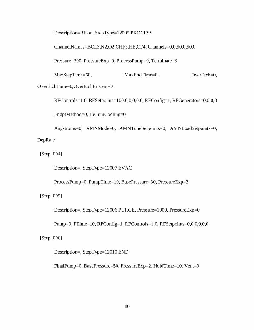
Description=RF on, StepType=12005 PROCESS
ChannelNames=BCL3,N2,O2,CHF3,HE,CF4, Channels=0,0,50,0,50,0
Pressure=300, PressureExp=0, ProcessPump=0, Terminate=3
MaxStepTime=60, MaxEndTime=0, OverEtch=0,
OverEtchTime=0,OverEtchPercent=0
RFControls=1,0, RFSetpoints=100,0,0,0,0,0, RFConfig=1, RFGenerators=0,0,0,0
EndptMethod=0, HeliumCooling=0
Angstroms=0, AMNMode=0, AMNTuneSetpoints=0, AMNLoadSetpoints=0,
DepRate=
[Step_004]
Description=, StepType=12007 EVAC
ProcessPump=0, PumpTime=10, BasePressure=30, PressureExp=2
[Step_005]
Description=, StepType=12006 PURGE, Pressure=1000, PressureExp=0
Pump=0, PTime=10, RFConfig=1, RFControls=1,0, RFSetpoints=0,0,0,0,0,0
[Step_006]
Description=, StepType=12010 END
FinalPump=0, BasePressure=50, PressureExp=2, HoldTime=10, Vent=0
80

REFERENCES
[1] Th. Udem, R. Holzwarth, and T. W. Hänsch, “Optical Frequency Metrology”, Nature
416, pp. 233-237, 2002.
[2] P. J. Delfyett, I. Ozdur, N. Hoghooghi, M. Akbulut, J. Davila-Rodriguez, and S.
Bhooplapur, “Advanced Ultrafast Technologies Based on Optical Frequency
Combs”, IEEE Journal of Selected Topics in Quantum Electronics, vol. 18, no. 1,
pp. 258-274, 2012.
[3] M. G. Thompson, A. R. Rae, M. Xia, R. V. Penty, and I. H. White, “InGaAs Quantum-
Dot Mode-Locked Laser Diodes”, IEEE Journal of Selected Topics in Quantum
Electronics, vol. 15, no. 3, pp.661-672, 2009.
[4] E. U. Rafailov, M. A. Cataluna, and W. Sibbett, “Mode-Locked Quantum-Dot Lasers”,
Nature Photonics 1, 395, 2007.
[5] X. Huang, A. Stintz, H. Li, L. F. Lester, J. Cheng and K. J. Malloy, “Passive Mode-
Locking in 1.3 μm Two-Section InAs Quantum Dot Lasers”, Applied Physics
Letters, vol. 78, no. 19 , pp. 2825-2827, 2001.
[6] D. J. Derickson, P. A. Morton, J. E. Bowers, and R. L. Thornton, “Comparison of
Timing Jitter in External and Monolithic Cavity Mode-Locked Semiconductor
Lasers”, Applied Physics Letters, vol. 59, no.26 , pp. 3372-3374, 1991.
[6] L. Drzewietzki, S. Breuer, and W. Elsäßer, “Timing jitter reduction of passively mode-
locked semiconductor lasers by self- and external-injection: numerical description
and experiments,” Optics Express, vol. 21, no. 13, pp. 16142-16161, Jun, 2013.
81

[7] D. J. Derickson, “Multi-Section Mode-Locked Semiconductor Lasers,” Ph.D.
dissertation, University of California, Santa Barbara, 1992.
[8] X. S. Yao, L. Davis and L. Maleki, “Coupled Optoelectronic Oscillators for Generating
Both RF Signal and Optical Pulses”, Journal of Lightwave Technology, vol. 18,
no.1, pp. 73-78, 2000.
[9] B. K. Mathason, and P. J. Delfyett, “Pulsed Injection Locking Dynamics of Passively
Mode-Locked External-Cavity Semiconductor Laser Systems for All-Optical
Clock Recovery”, Journal of Lightwave Technology, vol. 18, no.8 , pp. 1111-1120,
2000.
[10] S. Arahira and Y. Ogawa, “Synchronous Mode-Locking in Passively Mode-Locked
Semiconductor Laser Diodes Using Optical Short Pulses Repeated at
Subharmonics of the Cavity Round-Trip Frequency”, IEEE Photonics Technology
Letters, vol. 8, no. 2, pp. 191-193, 1996.
[11] P. Del´Haye, A. Schliesser, O. Arcizet, T. Wilken, R. Holzwarth and T. J. Kippenberg,
“Optical Frequency Comb Generation from a Monolithic Microresonator”, Nature
450, pp. 1214, 2007.
[12] S. Arahira, and Y. Ogawa, “480-GHz Sub-harmonic Synchronous Mode-locking in a
Short-cavity Colliding-pulse Mode-locked Laser Diode”, IEEE Photonics
Technology Letters, vol. 14, no. 4, pp. 537-539, 2002.
[13] Y. K. Chen, and M. C. Wu, “Monolithic Colliding-pulse Mode-locked Quantum-well
Lasers”, IEEE Journal of Quantum Electronics, vol. 28, no. 10, pp. 2176-2185,
1992.
82

[14] P. Vasil’ev, Ultrafast Diode Lasers: Fundamentals and Applications (London: Artech
House, 1995).
[15] F. Quinlan, S. Ozharar, S. Gee, and P. J. Delfyett, "Harmonically Mode-locked
Semiconductor-based Lasers as High Repetition Rate Ultralow Noise Pulse Train
and Optical Frequency Comb Sources," Journal of Optics A: Pure and Applied
Optics, vol. 11, no. 10, 2009.
[16] D. Kühlke, W. Rudolph, and B. Wilhelmi, “Influence of Transient Absorber Gratings
on the Pulse Parameters of Passively Mode-Locked CW Dye Ring Lasers, Applied
Physics Letters, vol. 42, no. 4, pp. 325-327, 1983.
[17] J. Buchert, R. Dorsinville, P. Delfyett, S. Krimchansky, and R. R. Alfano,
“Determination of Temporal Correlation of Ultrafast Laser Pulses Using Phase
Conjugation”, Optics Communications, vol. 52, no. 6, pp. 433-437, 1985.
[18] H. K. Lee, V. Loyo-Maldonado, B. C. Qiu, K. L. Lee, C. Shu, S. Pinches, I. G. Thayne,
A. C. Bryce, and J. H. Marsh, “Efficient Direct Locking of Colliding Pulse Mode-
Locked Lasers on Semi-Insulating Substrate at 1.5 μm”, IEEE Photonics
Technology Letters, vol. 14, no. 8, pp. 1049-1051, 2002.
[19] S. Arahira, S. Kutsuzawa and Y. Ogawa, “Extreme Timing Jitter Reduction of a
Passively Mode-Locked Laser Diode by Optical Pulse Injection”, IEEE Journal of
Quantum Electronics, vol. 35, no. 12, pp. 1805-1811, 1999.
[20] H. C. Bao and H. F. Liu, “Amplitude Noise of Subharmonically Hybrid Mode-Locked
Pulses Generated From a Monolithic Semiconductor Laser”, IEEE Photonics
Technology Letters, vol. 14, no. 1, pp. 6-8, 2002.
83

[21] M. T. Choi, J. M. Kim, W. Lee, and P. J. Delfyett, “Ultralow Noise Optical Pulse
Generation in an Actively Mode-locked Quantum-dot Semiconductor Laser”,
Applied Physics Letters, vol. 88, no. 13, pp. 131106-131108, 2006.
[22] M. Laemnlin, G. Fiol, C. Meur, M. Kuntz, F. Hopfer, A. R. Kovsh, N. N. Ledentsov,
and D. Bimberg, “Distortion-free Optical Amplification of 20-80 GHz Modelocked
Laser Pulses at 1.3 μm using Quantum Dots”, Electronics Letters, vol. 42, no. 12,
pp.697-699, 2006.
[23] C. E. Zah, R. Bhat, S. G. Menocal, N. Andreadakis, F. Favire, C. Caneau, M. A. Koza,
and T. P. Leee, “1.5 μm GaInAsP Angled-Facet Flared-Waveguide Traveling-
Wave Laser Amplifiers, IEEE Photonics Technology Letters, vol. 2, no. 1, pp. 46-
47, 1990.
[24] I. P. Kaminow, G. Eisenstein, and L. W. Stulz, “Measurement of the Modal
Reflectivity of an Antireflection Coating on a Superluminescent Diode”, IEEE
Journal of Quantum Electronics, vol. 19, no. 4, pp. 493-495, 1983.
[25] D. J. Derickson, Fiber Optic Test and Measurement (Prentice Hall, New Jersey, 1998),
p.185.
[26] C. van Dam, F. P. G. M. van Ham, F. H. Groen, J. J. G. M. van der Tol, I. Moerman,
and M. K. Smit, “Compact InP-based Waveguide Crossings with Low Crosstalk
and Low Loss”, in Conf. Proc. Integrated Photonics Research (Boston), vol. 6,
paper IMH-1, 1996.
[27] M. G. Daly, P. E. Jessop, and D. Yevick, “Crosstalk Reduction in Intersecting Rib
Waveguides”, Journal of Lightwave Technology”, vol. 14, no. 7, pp.1695-1698,
1996.
84

[28] Chen J., R. G. Broeke, Y. Du, Jing Cao, N. Chubun, P. Bjeletich, F. Olsson, S.
Lourdudoss, R. Welty, C. Reinhardt, P. L. Stephan, and S. J. B. Yoo, “Monolitically
integrated InP-based photonic chip development for O-CDMA systems,” IEEE
Journal of Selected Topics in Quantum Electronics, vol. 11, no. 1, pp. 66-77, Jan.
2005.
[29] S. T. S. Cheung, F. M. Soares, J. H. Baek, B. Gaun, F. Olsson, S. Lourdudoss, and S.
J. B. Yoo, “Monolithically integrated 10-GHz ring colliding pulse mode-locked
laser for on-chip coherent communications,” in Conf. Proc. Conference on Lasers
and Electro-Optics (CLEO), paper CW1N.8, May 2012.
[30] G. Li, J. Yao, Y. Luo, H. Thacker, A. Mekis, X. Zheng, I. Shubin, J. Lee, K. Raj, J. E.
Cunningham, and A. V. Krishnamoorthy, “ Ultralow-loss, high-density SOI optical
waveguide routing for macrochip interconnects,” Optics Express, vol. 20, no. 11,
pp. 12035-12039, May 2012.
[31] J. F. Bauters, M. J. R. Heck, D. John, D. Dai, M. Tien, J. S. Barton, A. Leinse, R. G.
Heidmeman, D. J. Blumenthal, and J. E. Bowers, “Ultra-low-loss high-aspect-ratio
Si3N4 waveguides,” Optics Express, vol. 19, no. 4, pp. 3163-3174, Feb. 2011.
[32] M. Piels, J. F. Bauters, M. L. Davenport, M. J. R. Heck, and J. E. Bowers, “ Low-loss
silicon nitride AWG demultiplexer heterogeneously integrated with hybrid III-
V/silicon photodetectors”, Journal of Lightwave Technology, vol. 32, no. 4, pp. 1-
7, Feb. 2014.
[33] J. F. Bauters, M. J. R. Heck, D. D. John, J. S. Barton, C. M. Bruinink, A. Leinse, R. G.
Heidmeman, D. J. Blumenthal, and J. E. Bowers, “Planar waveguides with less than
85
0.1 dB/m propagation loss fabricated with wafer bonding,” Optics Express, vol. 19,
no. 24, pp. 24090-24101, Nov. 2011.
[34] E. Marchena, T. Creazzo, S. B. Krasulick, P. K. L. Yu, D. V. Orden, J. Y. Spann, C. C.
Bilvin, J. M. Dallesasse, P. Varangis, R. J. Stone, and A. Mizrahi, “Integrated
tunable CMOS laser for Si photonics”, in conference proceedings OFC/NFOEC
Postdeadline Papers, paper PDP5C.7, 2013.
[35] H. Chen, Y. Kuo and J. E. Bowers, “High speed silicon modulators”, in conference
proceedings OECC 2009, paper ThG1, Hong Kong, Jul. 2009.
[36] Y. Tang, H. Chen, S. Jain, J. D. Peters, U. Westergren, and J. E. Bowers, “ 50Gb/s
hybrid silicon traveling-wave electroabsorption modulator”, Optics Express, vol.
19, no. 7, pp. 5811-5816, Mar. 2011.
[37] I. A. Avrutsky, D. S. Ellis, A. Tager, H. Anis, and J. M. Xu, “Design of widely tunable
semiconductor lasers and the concept of binary superimposed gratings (BSG’s)”,
IEEE Journal of Quantum Electronics, vol. 34, no. 4, pp. 729-741, Apr. 1998.
[38] J. Kim, and P. J. Delfyett, “ Interband optical pulse injection locking of quantum dot
mode-locked semiconductor laser”, Optics Express, vol. 16, no. 15, pp. 11153-
11161, Jul. 2008.
[39] E. Sarailou, A. Ardey, and P. J. Delfyett, “Low noise ultrashort pulse generation by
direct RF modulation at 22 GHz from an AlGaInAs multiple quantum-well laser at
1.55 µm”, IEEE Photonics Technology Letters, vol. 24, no. 17, pp. 1561-1563, Sep.
2012.
86