omap4460 es1.x dm multimedia device (rev. a)
TRANSCRIPT

OMAP™
OMAP4460Multimedia Device
Engineering Sample ES1.0 ES1.1
Version A
Data Manual
Public Version
PRODUCTION DATA information is current as of publication date.Products conform to specifications per the terms of the TexasInstruments standard warranty. Production processing does notnecessarily include testing of all parameters.
Literature Number: SWPS046A
January 2012

WARNING: EXPORT NOTICERecipient agrees to not knowingly export or re-export, directly orindirectly, any product or technical data (as defined by the U.S., EU, andother Export Administration Regulations) including software, or anycontrolled product restricted by other applicable national regulations,received from Disclosing party under this Agreement, or any directproduct of such technology, to any destination to which such export orre-export is restricted or prohibited by U.S. or other applicable laws,without obtaining prior authorisation from U.S. Department of Commerceand other competent Government authorities to the extent required bythose laws. This provision shall survive termination or expiration of thisAgreement.
According to our best knowledge of the state and end-use of thisproduct or technology, and in compliance with the export controlregulations of dual-use goods in force in the origin and exportingcountries, this technology is classified as follows:
US ECCN: 3E991
EU ECCN: EAR99
And may require export or re-export license for shipping it in compliancewith the applicable regulations of certain countries.

Public Version
OMAP4460
www.ti.com SWPS046A –JANUARY 2012
Contents1 Introduction ...................................................................................................................... 21
1.1 About This Manual ........................................................................................................ 21
1.2 OMAP4460 MIPI® Disclaimer ........................................................................................... 22
1.3 Trademarks ................................................................................................................. 22
1.4 Community Resources .................................................................................................... 232 Terminal Description .......................................................................................................... 24
2.1 Terminal Assignments .................................................................................................... 24
2.2 Ball Characteristics ........................................................................................................ 25
2.3 Multiplexing Characteristics .............................................................................................. 702.4 Signal Descriptions ........................................................................................................ 87
2.4.1 External Memory Interfaces ................................................................................... 88
2.4.1.1 GPMC ............................................................................................... 88
2.4.1.2 LPDDR2 ............................................................................................. 902.4.2 Video Interfaces ................................................................................................. 93
2.4.2.1 Camera .............................................................................................. 93
2.4.2.2 Display ............................................................................................... 942.4.3 Serial Communication Interfaces ............................................................................. 97
2.4.3.1 HDQ/1-Wire ......................................................................................... 97
2.4.3.2 I2C .................................................................................................... 97
2.4.3.3 SmartReflex ™ ..................................................................................... 98
2.4.3.4 McBSP .............................................................................................. 98
2.4.3.5 PDM ................................................................................................. 99
2.4.3.6 DMIC ................................................................................................. 99
2.4.3.7 McASP .............................................................................................. 99
2.4.3.8 SLIMbus ® ......................................................................................... 100
2.4.3.9 HSI ................................................................................................. 100
2.4.3.10 McSPI .............................................................................................. 101
2.4.3.11 UART ............................................................................................... 101
2.4.3.12 USB ................................................................................................ 1022.4.4 Removable Media Interfaces ................................................................................ 104
2.4.4.1 MMC/SDIO ........................................................................................ 104
2.4.4.2 USIM ............................................................................................... 1062.4.5 Test Interfaces ................................................................................................. 106
2.4.5.1 JTAG ............................................................................................... 106
2.4.5.2 DPM ................................................................................................ 106
2.4.5.3 TPIU ................................................................................................ 107
2.4.5.4 STM ................................................................................................ 108
2.4.5.5 ATTILA ............................................................................................. 109
2.4.5.6 Video Encoder Test .............................................................................. 109
2.4.6 General-Purpose IOs ......................................................................................... 110
2.4.7 General-Purpose In ........................................................................................... 1142.4.8 System and Miscellaneous .................................................................................. 114
2.4.8.1 DM Timer .......................................................................................... 114
2.4.8.2 KeyPad ............................................................................................. 115
2.4.8.3 POP ................................................................................................ 115
Copyright © 2012, Texas Instruments Incorporated Contents 3

Public Version
OMAP4460
SWPS046A –JANUARY 2012 www.ti.com
2.4.8.4 System And Miscellaneous ..................................................................... 116
2.4.9 Power Supplies ................................................................................................ 1183 Electrical Characteristics .................................................................................................. 121
3.1 Absolute Maximum Ratings ............................................................................................. 121
3.2 Recommended Operating Conditions ................................................................................. 1253.3 DC Electrical Characteristics ........................................................................................... 129
3.3.1 GPMC DC Electrical Characteristics ....................................................................... 129
3.3.2 LPDDR2 DC Electrical Characteristics ..................................................................... 134
3.3.3 Camera DC Electrical Characteristics ...................................................................... 137
3.3.4 Display DC Electrical Characteristics ....................................................................... 140
3.3.5 HDQ/1-Wire DC Electrical Characteristics ................................................................. 141
3.3.6 I2C DC Electrical Characteristics ............................................................................ 142
3.3.7 Audio McBSP / PDM / DMIC DC Electrical Characteristics ............................................. 144
3.3.8 McSPI DC Electrical Characteristics ........................................................................ 146
3.3.9 UART DC Electrical Characteristics ........................................................................ 149
3.3.10 USB DC Electrical Characteristics .......................................................................... 152
3.3.11 MMC/SDIO DC Electrical Characteristics .................................................................. 158
3.3.12 USIM DC Electrical Characteristics ......................................................................... 161
3.3.13 JTAG DC Electrical Characteristics ......................................................................... 163
3.3.14 DPM DC Electrical Characteristics ......................................................................... 164
3.3.15 Keypad DC Electrical Characteristics ...................................................................... 166
3.3.16 System DC Electrical Characteristics ...................................................................... 1673.4 External Capacitors ...................................................................................................... 171
3.4.1 Voltage Decoupling Capacitors .............................................................................. 171
3.4.1.1 Core, MPU, IVA, Audio Voltage Decoupling .................................................. 171
3.4.1.2 IO Voltage Decoupling ........................................................................... 172
3.4.1.3 Analog Voltage Decoupling ..................................................................... 174
3.4.2 Output Capacitors ............................................................................................. 1783.5 Power-up and Power-down Sequences .............................................................................. 181
3.5.1 Power-Up Sequence .......................................................................................... 181
3.5.2 Power-Down Sequence ...................................................................................... 1824 Clock Specifications ........................................................................................................ 184
4.1 Input Clock Specifications .............................................................................................. 186
4.1.1 Input Clock Requirements ................................................................................... 186
4.1.2 sys_32k CMOS Input Clock ................................................................................. 1864.1.3 fref_xtalin CMOS Input Clock ................................................................................ 187
4.1.3.1 fref_xtal_in / fref_xtal_out External Crystal .................................................... 187
4.1.3.2 fref_xtal_in Squarer Input Clock ................................................................ 188
4.1.4 fref_slicer_in Input Clock ..................................................................................... 1894.2 Output Clocks Specifications ........................................................................................... 191
4.2.1 FREF Output Clocks .......................................................................................... 1914.3 DPLLs, DLLs Specifications ............................................................................................ 193
4.3.1 DPLLs Characteristics ........................................................................................ 194
4.3.2 DLLs Characteristics .......................................................................................... 196
4.3.3 DPLLs and DLLs Noise Isolation ............................................................................ 196
4.4 Internal 32-kHz Oscillator ............................................................................................... 1965 Timing Requirements and Switching Characteristics ........................................................... 197
4 Contents Copyright © 2012, Texas Instruments Incorporated

Public Version
OMAP4460
www.ti.com SWPS046A –JANUARY 2012
5.1 Timing Test Conditions .................................................................................................. 1975.2 Interface Clock Specifications .......................................................................................... 197
5.2.1 Interface Clock Terminology ................................................................................. 197
5.2.2 Interface Clock Frequency ................................................................................... 197
5.2.3 Clock Jitter Specifications .................................................................................... 197
5.2.4 Clock Duty Cycle Error ....................................................................................... 198
5.3 Timing Parameters ....................................................................................................... 1985.4 External Memory Interface .............................................................................................. 198
5.4.1 General-Purpose Memory Controller (GPMC) ............................................................ 199
5.4.1.1 GPMC/NOR Flash Interface—Synchronous Mode—100 MHz ............................. 199
5.4.1.2 GPMC/NOR Flash Interface—Synchronous Mode—66 MHz .............................. 206
5.4.1.3 GPMC/NOR Flash Interface—Asynchronous Mode ......................................... 216
5.4.1.4 GPMC/NAND Flash Interface—Asynchronous Mode ....................................... 2245.4.2 External Memory Interface (EMIF) .......................................................................... 228
5.4.2.1 EMIF—DDR Mode ............................................................................... 2285.5 Multimedia Interfaces .................................................................................................... 243
5.5.1 Camera Interface .............................................................................................. 243
5.5.1.1 Camera Serial Interface (CSI2) ................................................................. 244
5.5.1.2 Camera Serial Interface (CCP2—CSI22) ..................................................... 246
5.5.1.3 Parallel Camera Interface (CPI) ................................................................ 2485.5.2 Display Subsystem Interface ................................................................................ 251
5.5.2.1 DSS—Display Controller (DISPC) .............................................................. 251
5.5.2.2 DSS—Remote Frame Buffer Interface (RFBI) Applications ................................ 254
5.5.2.3 Display Serial Interface (DSI1) .................................................................. 261
5.5.2.4 High Definition Multimedia Interface (HDMI) .................................................. 2635.6 Serial Communications Interfaces ..................................................................................... 263
5.6.1 Multichannel Buffered Serial Port (McBSP) ............................................................... 263
5.6.1.1 McBSP1, McBSP2, and McBSP3 Set#1 ...................................................... 264
5.6.1.2 McBSP3—I2S/PCM .............................................................................. 275
5.6.1.3 McBSP4—I2S/PCM .............................................................................. 281
5.6.2 Multichannel Buffered Serial Port (McASP) ............................................................... 2865.6.3 Multichannel Serial Port Interface (McSPI) ................................................................ 288
5.6.3.1 McSPI—MCSPI Interface in Transmit and Receive—Slave Mode ........................ 289
5.6.3.2 McSPI—McSPI Interface in Transmit and Receive—Master Mode ........................ 294
5.6.4 Digital Microphone (DMIC) ................................................................................... 305
5.6.5 Multichannel Pulse Density Modulation (McPDM) ........................................................ 3085.6.6 SlimBus ......................................................................................................... 311
5.6.6.1 ABE SlimBus1, SlimBus2—SLIMBUS SDR 24.6 MHz ...................................... 311
5.6.6.2 ABE SlimBus1, SlimBus2—SLIMBUS SDR 19.2 MHz ...................................... 3135.6.7 High-Speed Synchronous Interface (HSI) ................................................................. 315
5.6.7.1 High-Speed Synchronous Interface 1 .......................................................... 315
5.6.7.2 High-Speed Synchronous Interface 2 .......................................................... 3175.6.8 Universal Serial Bus (USB) .................................................................................. 321
5.6.8.1 Universal Serial Bus (USB)—USBA0 .......................................................... 321
5.6.8.2 Universal Serial Bus (USB)—USBC1 .......................................................... 322
5.6.8.3 Universal Serial Bus (USB)—USBB1 .......................................................... 327
5.6.8.4 Universal Serial Bus (USB)—USBB2 .......................................................... 338
Copyright © 2012, Texas Instruments Incorporated Contents 5

Public Version
OMAP4460
SWPS046A –JANUARY 2012 www.ti.com
5.6.9 Inter-Integrated Circuit Interface (I2C) ...................................................................... 349
5.6.9.1 I2C and SmartReflex—Standard and Fast Modes ........................................... 350
5.6.9.2 I2C and SmartReflex—High-Speed Mode ..................................................... 3515.6.10 HDQ / 1-Wire Interface (HDQ/1-Wire) ...................................................................... 352
5.6.10.1 HDQ / 1-Wire—HDQ Mode ..................................................................... 352
5.6.10.2 HDQ/1-Wire—1-Wire Mode ..................................................................... 3545.6.11 Universal Asynchronous Receiver Transmitter (UART) .................................................. 355
5.6.11.1 UART3 IrDA ....................................................................................... 3625.7 Removable Media Interfaces ........................................................................................... 365
5.7.1 Multimedia Memory Card and Secure Digital IO Card (SDMMC) ...................................... 365
5.7.1.1 MMC/SD/SDIO 1 Interface ...................................................................... 365
5.7.1.2 MMC/SD/SDIO 2 Interface ...................................................................... 374
5.7.1.3 MMC/SD/SDIO 3, 4, and 5 Interfaces ......................................................... 381
5.7.2 Universal Subscriber Identity Module Interface (USIM) .................................................. 3845.8 Test Interfaces ............................................................................................................ 385
5.8.1 Digital Processing Manager Interface (DPM) .............................................................. 385
5.8.1.1 Trace Port Interface Unit (TPIU) ................................................................ 385
5.8.1.2 System Trace Module Interface (STM) ........................................................ 3865.8.2 JTAG Interface (JTAG) ....................................................................................... 390
5.8.2.1 JTAG—Free-Running Clock Mode ............................................................. 390
5.8.2.2 JTAG—Adaptive Clock Mode ................................................................... 392
5.8.3 cJTAG Interface (cJTAG) .................................................................................... 3936 Thermal Management ....................................................................................................... 396
6.1 Package Thermal Characteristics ...................................................................................... 3966.2 Temperature Sensor Recommendation ............................................................................... 397
6.2.1 PCB Temperature Sensor ................................................................................... 397
6.2.2 Junction Temperature Sensor ............................................................................... 3977 Package Characteristics ................................................................................................... 399
7.1 Device Nomenclature .................................................................................................... 399
7.1.1 Standard Package Symbolization ........................................................................... 399
7.1.2 SAP Part Number ............................................................................................. 400
7.1.3 Device Naming Convention .................................................................................. 400
7.2 Mechanical Data ......................................................................................................... 401A OMAP4460 Processor Multimedia Device PCB Guideline ...................................................... 402
A.1 Introduction ............................................................................................................... 402A.2 Initial Requirements and Guidelines ................................................................................... 402
A.2.1 Introduction to the PCB Guidelines ......................................................................... 402A.2.2 PCB Power General Routing Guidelines ................................................................... 404
A.2.2.1 Step 1: PCB Stack-up Guidelines .............................................................. 404
A.2.2.2 Step 2: Physical Layout Guidelines of the PDN .............................................. 406
A.2.2.3 Step 3: Static IR Drop PDN Guidelines ........................................................ 410
A.2.3 Lumped and Distributed Resistance/IR Drop Analysis Methodology .................................. 411A.2.4 System ESD Generic Guidelines ............................................................................ 412
A.2.4.1 IEC61000-4-2 Standard Overview—System ESD ........................................... 412
A.2.4.2 Objective and Limitation of the Protection Strategy .......................................... 414
A.2.4.3 Concept of Isolation Impedance ................................................................ 414
A.2.4.4 System ESD Generic PCB Guideline .......................................................... 415
A.2.4.5 Miscellaneous EMC Guidelines to Mitigate ESD Immunity ................................. 415
6 Contents Copyright © 2012, Texas Instruments Incorporated
Public Version
OMAP4460
www.ti.com SWPS046A –JANUARY 2012
A.3 Single-Ended Interfaces ................................................................................................. 416
A.3.1 General Routing Guidelines ................................................................................. 416A.3.2 Single-Ended PCB Guideline in OMAP4 ................................................................... 417
A.3.2.1 OMAP4460 Single-Ended Interfaces—PCB Guideline ...................................... 417
A.3.2.2 OMAP4460 Single-Ended Interfaces—OMAP4460 System ESD Guideline ............. 420A.4 Differential Interface PCB Guidelines ................................................................................. 422
A.4.1 General Routing Guidelines ................................................................................. 422A.4.2 Three-step Design and Validation Methodology for OMAP Boards .................................... 423
A.4.2.1 Three-step Design and Validation Methodology—General Guidelines .................... 423
A.4.2.2 Step 1: General Guidelines for OMAP Boards ............................................... 425
A.4.2.3 Step 2: Length Mismatch Guidelines for OMAP Boards .................................... 425
A.4.2.4 Step 3: Frequency-domain Specification Guidelines for OMAP Boards .................. 426A.4.3 MIPI D-PHY PCB Guidelines in OMAP4 ................................................................... 431
A.4.3.1 CSI21 and CSI22 MIPI CSI-2 @ 1 Gbps (Up to 3 Data Lanes, OPP100), @ 824 Mbps (Upto 4 Data Lanes, OPP100), @ 800 Mbps (Up to 4 Data Lanes, OPP50) Device PCBGuidelines ......................................................................................... 431
A.4.3.2 DSI1 and DSI2 MIPI DSI1 @ 900 Mbps (Up to 3 Data Lanes), @ 824 Mbps (Up to 4 DataLanes) Device PCB Guideline .................................................................. 433
A.4.4 USBA0 PHY Interface in OMAP4 ........................................................................... 435
A.4.4.1 USBA0 PHY PCB Guideline .................................................................... 435
A.4.4.2 USBA0 PHY Implementation Example ........................................................ 436
A.4.4.3 ESD Implementation—USBA0 PHY ........................................................... 437
A.4.5 HDMI Interface in OMAP4 ................................................................................... 437A.5 Clock Guidelines ......................................................................................................... 437
A.5.1 32-kHz Oscillator Routing .................................................................................... 438
A.5.2 Oscillator Ground Connection ............................................................................... 438
A.5.3 Electromagnetic Interference (EMI) Prevention in Clock Distribution .................................. 439A.6 Ground Guidelines ....................................................................................................... 440
A.6.1 Guard Ring on PCB Edges .................................................................................. 440
A.6.2 Analog and Digital Ground ................................................................................... 440B Glossary ......................................................................................................................... 441
B.1 Glossary ................................................................................................................... 441
Copyright © 2012, Texas Instruments Incorporated Contents 7
Public Version
OMAP4460
SWPS046A –JANUARY 2012 www.ti.com
List of Figures2-1 S-PBGA-N547 Package (Bottom View) ....................................................................................... 24
2-2 S-PBGA-N547 Package (Top View) ........................................................................................... 25
3-1 Output Turn-on Time Measurement .......................................................................................... 136
3-2 Output Supply Noise Measurement Setup .................................................................................. 136
3-3 HDMI Power PCB Routing Topology......................................................................................... 175
3-4 DPLLs / Complex I/Os VDDA Power PCB Routing Topology ............................................................ 176
3-5 OMAP Embedded LDO / Bandgap Power PCB Routing Topology ...................................................... 177
3-6 External Capacitors—Page 1 of 2 ............................................................................................ 179
3-7 External Capacitors—Page 2 of 2 ............................................................................................ 180
3-8 Power-Up Sequence ........................................................................................................... 181
3-9 Power-Down Sequence ........................................................................................................ 183
4-1 Clock Interface ................................................................................................................. 185
4-2 sys_32k Input Clock ............................................................................................................ 187
4-3 Crystal Implementation......................................................................................................... 187
4-4 fref_xtal_in Squarer Input Clock .............................................................................................. 189
4-5 fref_slicer_in Input Clock....................................................................................................... 190
4-6 fref_clkx_out Output Clocks ................................................................................................... 193
5-1 Cycle (or Period) Jitter ......................................................................................................... 197
5-2 GPMC / Multiplexed 16-bit NOR Flash—Synchronous Single Read .................................................... 203
5-3 GPMC / Nonmultiplexed 16-bit NOR Flash—Synchronous Single Read ............................................... 204
5-4 GPMC / Multiplexed 16-bit NOR Flash—Synchronous Burst Read 4x16 Bits.......................................... 205
5-5 GPMC / Nonmultiplexed 16-bit NOR Flash—Synchronous Burst Read 4x16 Bits..................................... 206
5-6 GPMC / Multiplexed 16-bit NOR Flash—Synchronous Single Read .................................................... 211
5-7 GPMC / Nonmultiplexed 16-bit NOR Flash—Synchronous Single Read ............................................... 212
5-8 GPMC / Multiplexed 16-bit NOR Flash—Synchronous Burst Read 4x16 Bits.......................................... 213
5-9 GPMC / Nonmultiplexed 16-bit NOR Flash—Synchronous Burst Read 4x16 Bits..................................... 214
5-10 GPMC / Multiplexed 16-bit NOR Flash—Synchronous Burst Write 4 x 16 Bits ........................................ 215
5-11 GPMC / Nonmultiplexed 16-bit NOR Flash—Synchronous Burst Write 4 x 16 Bits ................................... 216
5-12 GPMC / NOR Flash—Asynchronous Read—Single Word Timing ....................................................... 219
5-13 GPMC / NOR Flash—Asynchronous Read—32-bit Timing ............................................................... 220
5-14 GPMC / NOR Flash—Asynchronous Read—Page Mode 4x16-bit Timing.............................................. 221
5-15 GPMC / NOR Flash—Asynchronous Write—Single Word Timing ....................................................... 222
5-16 GPMC / Multiplexed NOR Flash—Asynchronous Read—Single Word Timing......................................... 223
5-17 GPMC / Multiplexed NOR Flash—Asynchronous Write—Single Word Timing......................................... 224
5-18 GPMC / NAND Flash—Asynchronous Mode—Command Latch Cycle Timing ........................................ 226
5-19 GPMC / NAND Flash—Asynchronous Mode—Address Latch Cycle Timing ........................................... 227
5-20 GPMC / NAND Flash—Asynchronous Mode—Data Read Cycle Timing ............................................... 227
5-21 GPMC / NAND Flash—Asynchronous Mode—Data Write Cycle Timing ............................................... 228
5-22 EMIF—DDR Mode—DQ / DM / DQS Read Parameters .................................................................. 232
5-23 EMIF—DDR Mode—DQ / DM / DQS Boot Read Parameters ............................................................ 233
5-24 EMIF—DDR Mode—Output Clock Parameters............................................................................. 233
5-25 EMIF—DDR Mode—DQ / DM / DQS Write Parameters .................................................................. 234
5-26 EMIF—DDR Mode—CKE and Command Address Write Parameters .................................................. 234
5-27 EMIF—DDR Mode—CKE and Command Boot Write Parameters....................................................... 234
5-28 EMIF—DDR Mode—SDRAM Core Parameters—Self-Refresh Command ............................................. 235
5-29 EMIF—DDR Mode—SDRAM Core Parameters—Power-Down Exit Time Command ................................ 235
5-30 EMIF—DDR Mode—SDRAM Core Parameters—Deep Power-Down Command ..................................... 235
8 List of Figures Copyright © 2012, Texas Instruments Incorporated
Public Version
OMAP4460
www.ti.com SWPS046A –JANUARY 2012
5-31 EMIF—DDR Mode—SDRAM Core Parameters—Read to Read Command ........................................... 236
5-32 EMIF—DDR Mode—SDRAM Core Parameters—Read to Precharge .................................................. 236
5-33 EMIF—DDR Mode—SDRAM Core Parameters—Active to Read, Precharge, Active to Precharge, Write, Writeto Read, Active Bank A to Active Bank B Commands ..................................................................... 236
5-34 EMIF—DDR Mode—SDRAM Core Parameters—Write Recovery Time ................................................ 237
5-35 EMIF—DDR Mode—SDRAM Core Parameters—Write to Read Command ........................................... 237
5-36 EMIF—DDR Mode—SDRAM Core Parameters—Active to Active Command ......................................... 238
5-37 EMIF—DDR Mode—NVM Core Parameters—Active to Read or Write, Active Bank A to Active Bank B, Activeto Active, Precharge to Active, Active to Preactive Commands .......................................................... 238
5-38 EMIF—DDR Mode—NVM Core Parameters—Write Recovery Time Before Active................................... 239
5-39 EMIF—DDR Mode—NVM Core Parameters—CAS to CAS .............................................................. 239
5-40 EMIF—DDR Mode—NVM Core Parameters—Exit Power-Down to Next Valid Command........................... 240
5-41 EMIF—DDR Mode—Mode Register Parameters—Write Command .................................................... 240
5-42 EMIF—DDR Mode—Mode Register Parameters—Read Command .................................................... 240
5-43 EMIF—DDR Mode—ZQ Calibration Parameters ........................................................................... 240
5-44 CSI21 and CSI22—High-Speed Mode....................................................................................... 245
5-45 CSI21 and CSI22—Low-Power and Ultralow-Power Modes.............................................................. 246
5-46 CCP2—CSI22—Class 0 ....................................................................................................... 247
5-47 CCP2—CSI22—Class 1, Class 2............................................................................................. 247
5-48 CPI—Video and Graphics Digitizer—1.8-V Progressive Mode ........................................................... 249
5-49 CPI—Video and Graphics Digitizer—1.8-V Interlaced Mode ............................................................. 250
5-50 DSS—DISPC—QXGA SDR Application..................................................................................... 253
5-51 DSS—RFBI—Command / Data Write—LCD Panel........................................................................ 256
5-52 DSS—RFBI—Command / Data Read—LCD Panel........................................................................ 257
5-53 DSS—RFBI—Command / DataWrite to Read and Read to Write—LCD Panel........................................ 257
5-54 DSS—RFBI—Command / Data Write—Pico DLP.......................................................................... 260
5-55 DSS—DSI—High-Speed Mode ............................................................................................... 262
5-56 DSS—DSI—Low-Power and Ultralow-Power Modes ...................................................................... 263
5-57 McBSP1, 2—I2S/PCM—Master Mode....................................................................................... 267
5-58 McBSP1, 2—I2S/PCM—Slave Mode ........................................................................................ 267
5-59 McBSP1, 2, and 3 Set#1—TDM / Half-Cycle—Master Mode............................................................. 271
5-60 McBSP1, 2, and 3 Set#1—TDM / Half-Cycle—Slave Mode .............................................................. 271
5-61 McBSP1, 2, and 3 Set#1—TDM / Half-Cycle—Master Mode............................................................. 274
5-62 McBSP1, 2, and 3 Set#1—TDM / Half-Cycle—Slave Mode .............................................................. 275
5-63 McBSP3—I2S/PCM—Master Mode .......................................................................................... 280
5-64 McBSP3—I2S/PCM—Slave Mode ........................................................................................... 280
5-65 McBSP4—I2S/PCM—Master Mode .......................................................................................... 285
5-66 McBSP4—I2S/PCM—Slave Mode ........................................................................................... 286
5-67 McASP Output Timing ......................................................................................................... 288
5-68 McSPI—Slave Mode—Transmit .............................................................................................. 294
5-69 McSPI—Slave Mode—Receive ............................................................................................... 294
5-70 McSPI—Master Mode—Transmit............................................................................................. 303
5-71 McSPI—Master Mode—Transmit............................................................................................. 304
5-72 DMIC Implementation Example ............................................................................................... 306
5-73 DMIC—Master DDR Receive Mode.......................................................................................... 307
5-74 McPDM—Master Transmit SDR Mode ...................................................................................... 311
5-75 McPDM—Master Receive SDR Mode ....................................................................................... 311
5-76 ABE SlimBus1, SlimBus2 Master Read Mode .............................................................................. 312
5-77 ABE SlimBus1, SlimBus2 Master Write Mode .............................................................................. 313
Copyright © 2012, Texas Instruments Incorporated List of Figures 9
Public Version
OMAP4460
SWPS046A –JANUARY 2012 www.ti.com
5-78 ABE SlimBus1, SlimBus2 Master Read Mode .............................................................................. 314
5-79 ABE SlimBus1, SlimBus2 Master Write Mode .............................................................................. 314
5-80 HSI1, 2 Interfaces—1.2 V and 1.8 V—Receive Mode ..................................................................... 320
5-81 HSI1, 2 Interfaces—1.2 V and 1.8 V—Transmit Mode .................................................................... 320
5-82 High-Speed USB USBA0—ULPI SDR—Slave Mode—1.8 V............................................................. 322
5-83 Low- / Full-Speed USBC1—Bidirectional Standard 4-pin Mode—1.8 V................................................. 324
5-84 Low- / Full-Speed USBC1—Bidirectional Standard 4-pin TLL Mode—1.8 V ........................................... 326
5-85 Low- / Full-Speed USBC1—Bidirectional 2-pin Mode—1.8 V, 3.3 V .................................................... 327
5-86 Low- / Full-Speed USBB1—Bidirectional Standard 4-pin Mode—1.8 V................................................. 328
5-87 Low- / Full-Speed USBB1—Bidirectional TLL 4-pin Mode—1.8 V ....................................................... 330
5-88 Low- / Full-Speed USBB1—Bidirectional Standard 3-pin Mode—1.8 V................................................. 331
5-89 Low- / Full-Speed USBB1—Bidirectional TLL 3-pin Mode—1.8 V ....................................................... 333
5-90 High-Speed USBB1—ULPI SDR Mode—Slave Mode—1.8 V............................................................ 334
5-91 High-Speed USBB1—ULPI TLL Mode—Master Mode—1.8 V ........................................................... 336
5-92 High-Speed USBB1—HSIC DDR Receive And Transmit Modes—1.2 V ............................................... 338
5-93 Low- / Full-Speed USBB2—Bidirectional Standard 4-pin Mode—1.8 V................................................. 339
5-94 Low- / Full-Speed USBB2—Bidirectional TLL 4-pin Mode—1.8 V ....................................................... 341
5-95 Low- / Full-Speed USBB2—Bidirectional Standard 3-pin Mode—1.8 V................................................. 342
5-96 Low- / Full-Speed USBB2—Bidirectional TLL 3-pin Mode—1.8 V ....................................................... 343
5-97 Low- / Full-Speed USBB2—Bidirectional 2-pin Mode—1.8 V............................................................. 344
5-98 High-Speed USBB2—ULPI SDR Mode—Slave Mode..................................................................... 346
5-99 High-Speed USBB2—ULPI TLL Mode—Master Mode .................................................................... 348
5-100 High-Speed USBB2—HSIC DDR Receive And Transmit Modes—1.2 V ............................................... 349
5-101 I2C and SmartReflex—Standard and Fast Modes.......................................................................... 351
5-102 I2C and SmartReflex—High-Speed Mode ................................................................................... 352
5-103 HDQ Break and Break Recovery Timing—OMAP HDQ Interface Writing to Slave.................................... 353
5-104 HDQ Break Detection—OMAP HDQ Interface Reading to Slave ........................................................ 353
5-105 OMAP HDQ Interface Bit Read Timing (Data).............................................................................. 354
5-106 OMAP HDQ Interface Bit Write Timing (Command / Address or Data) ................................................. 354
5-107 HDQ Communication Timing .................................................................................................. 354
5-108 1-Wire—Break (Reset) ......................................................................................................... 355
5-109 1-Wire—Read Bit (Data) ....................................................................................................... 355
5-110 1-Wire—Write Bit-One Timing (Command / Address or Data) ........................................................... 355
5-111 1-Wire—Write Bit-Zero Timing (Command / Address or Data) ........................................................... 355
5-112 UART IrDA Pulse Parameters ................................................................................................ 363
5-113 MMC/SD/SDIO 1 Interface—SD Identification and Standard SD—Transmitter Mode ................................ 367
5-114 MMC/SD/SDIO 1 Interface—SD Identification and Standard SD—Receiver Mode ................................... 367
5-115 MMC/SD/SDIO 1 Interface—High-Speed SD Mode—Transmitter Mode ............................................... 369
5-116 MMC/SD/SDIO 1 Interface—High-Speed SD Mode—Receiver Mode .................................................. 370
5-117 MMC/SD/SDIO 1 Interface—High-Speed SDR50—Transmitter Mode .................................................. 371
5-118 MMC/SD/SDIO 1 Interface—High-Speed SDR50—Receiver Mode ..................................................... 371
5-119 MMC/SD/SDIO 1 Interface—High-Speed SD—DDR50—Data/Command Transmit .................................. 373
5-120 MMC/SD/SDIO 1 Interface—High-Speed SD—DDR50—Data/Command Receive ................................... 373
5-121 MMC/SD/SDIO 2 Interface—High-Speed SDR JC64—Transmitter Mode .............................................. 376
5-122 MMC/SD/SDIO 2 Interface—High-Speed SDR JC64—Receiver Mode ................................................. 376
5-123 MMC/SD/SDIO 2 Interface—High-Speed DDR JC64—Receiver Mode................................................. 378
5-124 MMC/SD/SDIO 2 Interface—High-Speed DDR JC64—Transmitter Mode.............................................. 379
5-125 MMC/SD/SDIO 2 Interface—Standard SDR JC64—Transmitter Mode ................................................. 380
10 List of Figures Copyright © 2012, Texas Instruments Incorporated

Public Version
OMAP4460
www.ti.com SWPS046A –JANUARY 2012
5-126 MMC/SD/SDIO 2 Interface—Standard SDR JC64—Receiver Mode .................................................... 381
5-127 MMC/SD/SDIO 3, 4, and 5 Interfaces—High-Speed SDIO—Transmitter Mode ....................................... 383
5-128 MMC/SD/SDIO 3, 4, and 5 Interfaces—High-Speed SDIO—Receiver Mode .......................................... 383
5-129 USIM—Clock Specification .................................................................................................... 384
5-130 USIM—Transmit Mode......................................................................................................... 384
5-131 USIM—Receive Mode.......................................................................................................... 385
5-132 TPIU—PLL DDR Transmit Mode ............................................................................................. 386
5-133 STM—Lauterbach DDR Transmit Mode ..................................................................................... 388
5-134 STM—MIPI DDR Transmit Mode ............................................................................................. 389
5-135 STM—MIPI SDR Transmit Mode ............................................................................................. 390
5-136 JTAG Interface Timing—Free-running Clock Mode ........................................................................ 392
5-137 JTAG Interface Timing—Adaptive Clock Mode ............................................................................. 393
5-138 cJTAG Interface Timing—Normal Mode ..................................................................................... 395
6-1 PCB Temperature Sensor Recommendation ............................................................................... 397
7-1 Printed Device Reference ..................................................................................................... 399
7-2 Production Mechanical Package.............................................................................................. 401
A-1 Minimize Loop Inductance With Proper Layer Assignment ............................................................... 404
A-2 Layer PCB With High Density Interconnect (HDI) Vias .................................................................... 405
A-3 Layer PCB With Plated Though Holes (PTH) Vias ......................................................................... 405
A-4 Poor Via Assignment for PDN................................................................................................. 406
A-5 Improved Via Assignment for PDN ........................................................................................... 407
A-6 Via Starvation ................................................................................................................... 408
A-7 Improved Layout With More Transitional Vias .............................................................................. 408
A-8 Coplanar Shielding of Power Net Using Ground Guard-band ............................................................ 408
A-9 Characteristics of a Real Capacitor With ESL and ESR................................................................... 409
A-10 Series Model Impedance Equation ........................................................................................... 409
A-11 Typical Impedance Profile of a Capacitor ................................................................................... 409
A-12 Capacitor Placement Geometry for Improved Mounting Inductance..................................................... 410
A-13 Depiction of Sheet Resistivity and Resistance.............................................................................. 411
A-14 Static IR Drop Budget for PCB Only ......................................................................................... 411
A-15 Pin-grouping Concept: Lumped and Distributed Methodologies ......................................................... 412
A-16 IEC61000-4-2 Waveform ...................................................................................................... 413
A-17 Simplified Current Distribution ................................................................................................ 414
A-18 Placement Recommendation for an ESD External Protection............................................................ 415
A-19 Trace Examples................................................................................................................. 416
A-20 SDMMC1 Implementation Proposal With External SD Card.............................................................. 420
A-21 JTAG ESD Protection Example............................................................................................... 422
A-22 Summary of Three-step PCB Design and Validation Methodology for OMAP4 Differential Interfaces ............. 424
A-23 Transmission Line Interconnect System (TLIS)............................................................................. 424
A-24 Ground Guard Illustration ...................................................................................................... 425
A-25 Port Assignment for the Intralane Frequency-domain Specification ..................................................... 427
A-26 Intralane Sdd12 Frequency-domain Specification.......................................................................... 427
A-27 Sdd11/Sd22 Frequency-domain Specification .............................................................................. 428
A-28 Intralane Scc11/Scc22 Frequency-domain Specification.................................................................. 428
A-29 Intralane Scd11, Scd12, Sdc11, Sdc12 Frequency-domain Specification .............................................. 429
A-30 Port Assignment for the Interlane Frequency-domain Specification ..................................................... 430
A-31 Interlane Sdd11 / Sdd22 Frequency-domain Specification................................................................ 430
A-32 Interlane Scc11 / Scc22 Frequency-domain Specification ................................................................ 431
Copyright © 2012, Texas Instruments Incorporated List of Figures 11
Public Version
OMAP4460
SWPS046A –JANUARY 2012 www.ti.com
A-33 USB Implementation Proposal with TWL6030 PMIC ...................................................................... 437
A-34 Slow Clock PCB Requirements ............................................................................................... 438
A-35 Poor Oscillator Ground Connection .......................................................................................... 439
A-36 Optimized Oscillator Ground Connection .................................................................................... 439
A-37 Field Lines of a Signal Above Ground ....................................................................................... 440
A-38 Guard Ring Routing ............................................................................................................ 440
12 List of Figures Copyright © 2012, Texas Instruments Incorporated

Public Version
OMAP4460
www.ti.com SWPS046A –JANUARY 2012
List of Tables2-1 Ball Characteristics............................................................................................................... 28
2-2 Multiplexing Characteristics ..................................................................................................... 70
2-3 GPMC Signal Descriptions...................................................................................................... 88
2-4 LPDDR2 Signal Descriptions ................................................................................................... 90
2-5 Camera Control Signal Descriptions........................................................................................... 93
2-6 Camera Parallel Signal Descriptions .......................................................................................... 93
2-7 CSI21 Signal Descriptions ...................................................................................................... 93
2-8 CSI22 Signal Descriptions ...................................................................................................... 94
2-9 RFBI Signal Descriptions........................................................................................................ 94
2-10 DSI1 Signal Descriptions ........................................................................................................ 95
2-11 DSI2 Signal Descriptions ........................................................................................................ 95
2-12 CVIDEO Signal Descriptions ................................................................................................... 95
2-13 HDMI Signal Descriptions ....................................................................................................... 96
2-14 DISPC Signal Descriptions...................................................................................................... 96
2-15 HDQ/1-Wire Signal Descriptions ............................................................................................... 97
2-16 I2C Signal Descriptions .......................................................................................................... 97
2-17 SmartReflex Signal Descriptions ............................................................................................... 98
2-18 McBSP1, 2, 3 Signal Descriptions ............................................................................................. 98
2-19 McBSP4 Signal Descriptions ................................................................................................... 98
2-20 ABE McPDM Signal Descriptions .............................................................................................. 99
2-21 ABE DMIC Signal Descriptions................................................................................................. 99
2-22 ABE McASP Signal Descriptions............................................................................................... 99
2-23 ABE SLIMbus1 Signal Descriptions .......................................................................................... 100
2-24 SLIMbus2 Signal Descriptions ................................................................................................ 100
2-25 HSI Signal Descriptions ........................................................................................................ 100
2-26 McSPI Signal Descriptions .................................................................................................... 101
2-27 UART Signal Descriptions ..................................................................................................... 101
2-28 USB Signal Descriptions....................................................................................................... 102
2-29 MMC/SDIO Signal Descriptions............................................................................................... 104
2-30 USIM Signal Descriptions...................................................................................................... 106
2-31 JTAG Signal Descriptions ..................................................................................................... 106
2-32 DPM Signal Descriptions ...................................................................................................... 106
2-33 TPIU 16-Bit Signal Descriptions .............................................................................................. 107
2-34 TPIU 18-Bit Signal Descriptions .............................................................................................. 107
2-35 STM Signal Descriptions....................................................................................................... 108
2-36 ATTILA Signal Descriptions ................................................................................................... 109
2-37 Video Encoder Test Signal Descriptions..................................................................................... 109
2-38 GPIO Signal Descriptions...................................................................................................... 110
2-39 GPIN Signal Descriptions...................................................................................................... 114
2-40 DM Timer Signal Descriptions ................................................................................................ 114
2-41 Keypad Signal Descriptions ................................................................................................... 115
2-42 POP Signal Descriptions....................................................................................................... 115
2-43 System and Miscellaneous Signal Descriptions ............................................................................ 116
2-44 Power Supplies Signal Descriptions.......................................................................................... 118
3-1 Absolute Maximum Rating Over Junction Temperature Range .......................................................... 121
3-2 Maximum Current Ratings at Ball Level ..................................................................................... 122
3-3 Recommended Operating Conditions........................................................................................ 125
Copyright © 2012, Texas Instruments Incorporated List of Tables 13

Public Version
OMAP4460
SWPS046A –JANUARY 2012 www.ti.com
3-4 GPMC DC Electrical Characteristics ......................................................................................... 130
3-5 LPDDR2 DC Electrical Characteristics....................................................................................... 134
3-6 Camera CSI2 DC Electrical Characteristics................................................................................. 137
3-7 Camera Control DC Electrical Characteristics .............................................................................. 138
3-8 Display DSI1 DC Electrical Characteristics.................................................................................. 140
3-9 HDQ/1-Wire DC Electrical Characteristics .................................................................................. 141
3-10 I2C DC Electrical Characteristics ............................................................................................. 142
3-11 Audio McBSP / PDM / DMIC DC Electrical Characteristics ............................................................... 144
3-12 McSPI DC Electrical Characteristics ......................................................................................... 146
3-13 UART DC Electrical Characteristics .......................................................................................... 149
3-14 USB DC Electrical Characteristics............................................................................................ 152
3-15 MMC/SDIO DC Electrical Characteristics ................................................................................... 158
3-16 USIM DC Electrical Characteristics .......................................................................................... 161
3-17 JTAG DC Electrical Characteristics .......................................................................................... 163
3-18 DPM DC Electrical Characteristics ........................................................................................... 164
3-19 Keypad DC Electrical Characteristics ........................................................................................ 166
3-20 System DC Electrical Characteristics ........................................................................................ 167
3-21 Core, MPU, IVA, Audio Voltage Decoupling Characteristics.............................................................. 172
3-22 IO Voltage Decoupling Characteristics....................................................................................... 173
3-23 Analog Voltage Decoupling Characteristics ................................................................................. 174
3-24 Output Capacitor Characteristics ............................................................................................. 178
4-1 Input Clock Requirements ..................................................................................................... 186
4-2 sys_32k Input Clock Electrical Characteristics.............................................................................. 186
4-3 sys_32k Input Clock Timing Requirements.................................................................................. 187
4-4 Crystal Electrical Characteristics ............................................................................................. 187
4-5 Oscillator Switching Characteristics—Crystal Mode ....................................................................... 188
4-6 Oscillator Electrical Characteristics—Bypass Mode........................................................................ 188
4-7 fref_xtal_in Squarer Input Clock Timing Requirements—Bypass Mode................................................. 188
4-8 fref_slicer_in Input Clock Electrical Characteristics ........................................................................ 189
4-9 fref_slicer_in Input Square Clock Timing Requirements................................................................... 189
4-10 fref_slicer_in Input Single-ended Sine Clock Timing Requirements ..................................................... 190
4-11 fref_clkx_out Output Clock Electrical Characteristics ...................................................................... 191
4-12 fref_clkx_out Output Clock Switching Characteristics...................................................................... 192
4-13 DPLL1 / DPLL2 / DPLL3 / DPLL4 / DPLL5 / DSI1 DPLL / DSI2 DPLL Characteristics ............................... 194
4-14 DPLL6/HDMI DPLL Characteristics .......................................................................................... 195
4-15 DLL Characteristics............................................................................................................. 196
4-16 Internal 32-kHz Oscillator Characteristic..................................................................................... 196
5-1 Timing Parameters ............................................................................................................. 198
5-2 GPMC/NOR Flash Timing Conditions—Synchronous Mode—100 MHz ................................................ 199
5-3 GPMC/NOR Flash Timing Requirements—Synchronous Mode—100 MHz ............................................ 199
5-4 GPMC/NOR Flash Switching Characteristics—Synchronous Mode—100 MHz ....................................... 200
5-5 GPMC/NOR Flash Timing Conditions—Synchronous Mode—66 MHz.................................................. 206
5-6 GPMC/NOR Flash Timing Requirements—Synchronous Mode—66 MHz ............................................. 207
5-7 GPMC/NOR Flash Switching Characteristics—Synchronous Mode—66 MHz ......................................... 207
5-8 GPMC/NOR Flash Timing Conditions—Asynchronous Mode ............................................................ 216
5-9 GPMC/NOR Flash—Asynchronous Mode—Internal Parameters ........................................................ 217
5-10 GPMC/NOR Flash Timing Requirements—Asynchronous Mode ........................................................ 217
5-11 GPMC/NOR Flash Switching Characteristics—Asynchronous Mode.................................................... 217
14 List of Tables Copyright © 2012, Texas Instruments Incorporated

Public Version
OMAP4460
www.ti.com SWPS046A –JANUARY 2012
5-12 GPMC/NAND Flash Timing Conditions—Asynchronous Mode........................................................... 224
5-13 GPMC/NAND—Asynchronous Mode—Internal Parameters .............................................................. 225
5-14 GPMC/NAND Flash Timing Requirements—Asynchronous Mode....................................................... 225
5-15 GPMC/NAND Flash Switching Characteristics—Asynchronous Mode .................................................. 225
5-16 EMIF Timing Conditions—DDR Mode ....................................................................................... 228
5-17 EMIF Timing Requirements—DDR Mode ................................................................................... 229
5-18 EMIF Switching Characteristics—DDR Mode............................................................................... 230
5-19 LPDDR2 Timing Requirements Correspondence Between Data Manual and LPDDR2 JEDECStandard—(JESD209-2A) ..................................................................................................... 241
5-20 LPDDR2 Switching Characteristics Correspondence Between Data Manual and LPDDR2 JEDECStandard—(JESD209-2A) ..................................................................................................... 241
5-21 CSI21 and CSI22 Timing Conditions—High-Speed Mode ................................................................ 244
5-22 CSI21 and CSI22 Timing Requirements—High-Speed Mode ............................................................ 244
5-23 CSI21 and CSI22 Timing Conditions—Low-Power and Ultralow-Power Modes ....................................... 245
5-24 CSI21 and CSI22 Timing Requirements—Low-Power and Ultralow-Power Modes ................................... 245
5-25 CCP2—CSI22—Timing Conditions........................................................................................... 246
5-26 CCP2—CSI22—Timing Requirements....................................................................................... 246
5-27 CPI Timing Conditions—Video and Graphics Digitizer 1.8-V Mode ..................................................... 248
5-28 CPI Timing Requirements—Video and Graphics Digitizer 1.8-V Mode ................................................. 248
5-29 DISPC Timing Conditions—QXGA SDR Mode ............................................................................. 251
5-30 DISPC Switching Characteristics—QXGA SDR Mode .................................................................... 252
5-31 DSS—RFBI Timing Conditions—LCD Panel................................................................................ 254
5-32 DSS—RFBI Timing Requirements—LCD Panel............................................................................ 254
5-33 DSS—RFBI Switching Characteristics—LCD Panel ....................................................................... 254
5-34 DSS—RFBI Registers Configuration—LCD Panel ......................................................................... 256
5-35 DSS—RFBI Timing Conditions—Pico DLP ................................................................................. 258
5-36 DSS—RFBI Switching Characteristics—Pico DLP ......................................................................... 258
5-37 DSS—RFBI Register Configuration—Pico DLP ............................................................................ 260
5-38 DSS—DSI Switching Characteristics—High-Speed Mode ................................................................ 261
5-39 DSS—DSI Timing Conditions—Low-Power and Ultralow-Power Modes................................................ 262
5-40 DSI Switching Characteristics—Low-Power and Ultralow-Power Modes ............................................... 262
5-41 McBSP1, 2 Timing Conditions—I2S/PCM................................................................................... 264
5-42 McBSP1, 2 Timing Requirements—I2S/PCM—Master Mode ............................................................ 264
5-43 McBSP1, 2 Switching Characteristics—I2S/PCM—Master Mode........................................................ 265
5-44 McBSP1, 2 Timing Requirements—I2S/PCM—Slave Mode.............................................................. 266
5-45 McBSP1, 2 Switching Characteristics—I2S/PCM—Slave Mode ......................................................... 266
5-46 McBSP1, McBSP2, and McBSP3 Set#1 Timing Conditions—TDM / Half-Cycle....................................... 268
5-47 McBSP1, McBSP2, and McBSP3 Set#1 Timing Requirements—TDM / Half-Cycle—Master Mode ................ 268
5-48 McBSP1, McBSP2, and McBSP3 Set#1 Switching Characteristics—TDM / Half-Cycle—Master Mode............ 269
5-49 McBSP1, 2, and 3 Set#1 Timing Requirements—TDM / Half-Cycle—Slave Mode.................................... 269
5-50 McBSP1, 2, and 3 Set#1 Switching Characteristics—TDM / Half-Cycle—Slave Mode ............................... 270
5-51 McBSP1, McBSP2, and McBSP3 Set#1 Timing Conditions—TDM / Half-Cycle....................................... 272
5-52 McBSP1, McBSP2, and McBSP3 Set#1 Timing Requirements—TDM / Half-Cycle—Master Mode ................ 272
5-53 McBSP1, McBSP2, and McBSP3 Set#1 Switching Characteristics—TDM / Half-Cycle—Master Mode............ 273
5-54 McBSP1, McBSP2, and McBSP3 Set#1 Timing Requirements—TDM / Half-Cycle—Slave Mode.................. 273
5-55 McBSP1, 2, and 3 Set#1 Switching Characteristics—TDM / Half-Cycle—Slave Mode ............................... 274
5-56 McBSP3 Timing Conditions—I2S/PCM ...................................................................................... 275
5-57 McBSP3 Timing Requirements—I2S/PCM—Master Mode ............................................................... 276
5-58 McBSP3 Switching Characteristics—I2S/PCM—Master Mode ........................................................... 276
Copyright © 2012, Texas Instruments Incorporated List of Tables 15

Public Version
OMAP4460
SWPS046A –JANUARY 2012 www.ti.com
5-59 McBSP3 Timing Requirements—I2S/PCM—Slave Mode................................................................. 278
5-60 McBSP3 Switching Characteristics—I2S/PCM—Slave Mode ............................................................ 279
5-61 McBSP4 Timing Conditions—I2S/PCM ...................................................................................... 281
5-62 McBSP4 Timing Requirements—I2S/PCM—Master Mode ............................................................... 281
5-63 McBSP4 Switching Characteristics—I2S/PCM—Master Mode ........................................................... 281
5-64 McBSP4 Timing Requirements—I2S/PCM—Slave Mode................................................................. 282
5-65 McBSP4 Switching Characteristics—I2S/PCM—Slave Mode ............................................................ 283
5-66 McBSP4 Timing Conditions—I2S/PCM ...................................................................................... 283
5-67 McBSP4 Timing Requirements—I2S/PCM—Master Mode ............................................................... 283
5-68 McBSP4 Switching Characteristics—I2S/PCM—Master Mode ........................................................... 284
5-69 McBSP4 Timing Requirements—I2S/PCM—Slave Mode................................................................. 284
5-70 McBSP4 Switching Characteristics—I2S/PCM—Slave Mode ............................................................ 285
5-71 McASP Timing Conditions ..................................................................................................... 286
5-72 McASP Switching Characteristics ............................................................................................ 287
5-73 McSPI1 Timing Conditions—Slave Mode ................................................................................... 289
5-74 McSPI1 Timing Requirements—Slave Mode ............................................................................... 289
5-75 McSPI1 Switching Characteristics—Slave Mode ........................................................................... 290
5-76 McSPI2 and McSPI4 Timing Conditions—Slave Mode .................................................................... 290
5-77 McSPI2 and McSPI4 Timing Requirements—Slave Mode................................................................ 291
5-78 McSPI2 and McSPI4 Switching Characteristics—Slave Mode ........................................................... 291
5-79 McSPI3 Timing Conditions—Slave Mode ................................................................................... 292
5-80 McSPI3 Timing Requirements—Slave Mode ............................................................................... 292
5-81 McSPI3 Switching Characteristics—Slave Mode ........................................................................... 293
5-82 McSPI1 Timing Conditions—Master Mode .................................................................................. 295
5-83 McSPI1 Timing Requirements—Master Mode .............................................................................. 295
5-84 McSPI1 Switching Requirements—Master Mode .......................................................................... 295
5-85 McSPI2 Timing Conditions—Master Mode—24 MHz ...................................................................... 296
5-86 McSPI2 Timing Requirements—Master Mode .............................................................................. 297
5-87 McSPI2 Switching Requirements—Master Mode .......................................................................... 297
5-88 McSPI2 Timing Conditions—Master Mode—48 MHz ...................................................................... 298
5-89 McSPI2 Timing Requirements—Master Mode .............................................................................. 298
5-90 McSPI2 Switching Requirements—Master Mode .......................................................................... 298
5-91 McSPI3 Timing Conditions—Master Mode .................................................................................. 299
5-92 McSPI3 Timing Requirements—Master Mode .............................................................................. 300
5-93 McSPI3 Switching Requirements—Master Mode .......................................................................... 300
5-94 McSPI4 Timing Conditions—Master Mode .................................................................................. 301
5-95 McSPI4 Timing Requirements—Master Mode .............................................................................. 301
5-96 McSPI4 Switching Requirements—Master Mode .......................................................................... 301
5-97 DMIC Timing Conditions—Master/Receive Mode .......................................................................... 305
5-98 DMIC Timing Requirements—Master/Receive Mode ...................................................................... 307
5-99 DMIC Switching Characteristics—Master/Receive Mode ................................................................. 307
5-100 McPDM Timing Conditions .................................................................................................... 308
5-101 McPDM Timing Requirements—Master and Receive SDR Mode ....................................................... 308
5-102 McPDM Switching Characteristics—Master and Transmit SDR Mode .................................................. 310
5-103 ABE SlimBus1, SlimBus2 Timing Conditions ............................................................................... 311
5-104 ABE SlimBus1, SlimBus2 Timing Requirements ........................................................................... 312
5-105 ABE SlimBus1, SlimBus2 Switching Characteristics....................................................................... 312
5-106 ABE SlimBus1, SlimBus2 Timing Conditions ............................................................................... 313
16 List of Tables Copyright © 2012, Texas Instruments Incorporated

Public Version
OMAP4460
www.ti.com SWPS046A –JANUARY 2012
5-107 ABE SlimBus1, SlimBus2 Timing Requirements ........................................................................... 313
5-108 ABE SlimBus1, SlimBus2 Switching Characteristics....................................................................... 314
5-109 HSI1 Timing Conditions—Transmit and Receive Modes—1.2 V......................................................... 315
5-110 HSI1 Timing Requirements—Receive Mode—1.2 V....................................................................... 315
5-111 HSI1 Switching Characteristics—Transmit Mode—1.2 V ................................................................. 316
5-112 HSI1 Timing Conditions—Transmit and Receive Modes—1.8 V......................................................... 316
5-113 HSI1 Timing Requirements—Receive Mode—1.8 V....................................................................... 316
5-114 HSI1 Switching Characteristics—Transmit Mode—1.8 V ................................................................. 317
5-115 HSI2 Timing Conditions—Transmit and Receive Modes—1.2 V......................................................... 317
5-116 HSI2 Timing Requirements—Receive Mode—1.2 V....................................................................... 318
5-117 HSI2 Switching Characteristics—Transmit Mode—1.2 V ................................................................. 318
5-118 HSI2 Timing Conditions—Transmit and Receive Modes—1.8 V......................................................... 319
5-119 HSI2 Timing Requirements—Receive Mode—1.8 V....................................................................... 319
5-120 HSI2 Switching Characteristics—Transmit Mode—1.8 V ................................................................. 319
5-121 High-Speed USB USBA0 Timing Conditions—ULPI SDR—Slave Mode—1.8 V ...................................... 321
5-122 High-Speed USB USBA0 Timing Requirements—ULPI SDR—Slave Mode—1.8 V .................................. 321
5-123 High-Speed HSUSB USBA0 Switching Characteristics—ULPI SDR—Slave Mode—1.8 V .......................... 322
5-124 Low- / Full-Speed USBC1 Timing Conditions—Bidirectional Standard 4-pin Mode—1.8 V .......................... 323
5-125 Low- / Full-Speed USBC1 Timing Requirements—Bidirectional Standard 4-pin Mode—1.8 V ...................... 324
5-126 Low- / Full-Speed USBC1 Switching Characteristics—Bidirectional Standard 4-pin Mode—1.8 V.................. 324
5-127 Low- / Full-Speed USBC1 Timing Conditions—Bidirectional Standard 4-pin TLL Mode—1.8 V..................... 325
5-128 Low- / Full-Speed USBC1 Timing Requirements—Bidirectional Standard 4-pin TLL Mode—1.8 V................. 325
5-129 Low- / Full-Speed USBC1 Switching Characteristics—Bidirectional Standard 4-pin TLL Mode—1.8 V ............ 325
5-130 Low- / Full-Speed USBC1 Timing Conditions—Bidirectional 2-pin Mode—1.8 V, 3.3 V .............................. 326
5-131 Low- / Full-Speed USBC1 Timing Requirements—Bidirectional 2-pin Mode—1.8 V, 3.3 V .......................... 327
5-132 Low- / Full-Speed USBB1 Timing Conditions—Bidirectional Standard 4-pin Mode—1.8 V .......................... 327
5-133 Low- / Full-Speed USBB1 Timing Requirements—Bidirectional Standard 4-pin Mode—1.8 V ...................... 328
5-134 Low- / Full-Speed USBB1 Switching Characteristics—Bidirectional Standard 4-pin Mode—1.8 V.................. 328
5-135 Low- / Full-Speed USBB1 Timing Conditions—Bidirectional TLL 4-pin Mode—1.8 V................................. 329
5-136 Low- / Full-Speed USBB1 Timing Requirements—Bidirectional TLL 4-pin Mode—1.8 V............................. 329
5-137 Low- / Full-Speed USBB1 Switching Characteristics—Bidirectional TLL 4-pin Mode—1.8 V ........................ 329
5-138 Low- / Full-Speed USBB1 Timing Conditions—Bidirectional Standard 3-pin Mode—1.8 V .......................... 330
5-139 Low- / Full-Speed USBB1 Timing Requirements—Bidirectional Standard 3-pin Mode—1.8 V ...................... 331
5-140 Low- / Full-Speed USBB1 Switching Characteristics—Bidirectional Standard 3-pin Mode—1.8 V.................. 331
5-141 Low- / Full-Speed USBB1 Timing Conditions—Bidirectional TLL 3-pin Mode—1.8 V................................. 331
5-142 Low- / Full-Speed USBB1 Timing Requirements—Bidirectional TLL 3-pin Mode—1.8 V............................. 332
5-143 Low- / Full-Speed USBB1 Switching Characteristics—Bidirectional TLL 3-pin Mode—1.8 V ........................ 332
5-144 High-Speed USBB1 Timing Conditions—ULPI SDR Mode—1.8 V ...................................................... 333
5-145 High-Speed USBB1 Timing Requirements—ULPI SDR Mode—Slave Mode—1.8 V ................................. 333
5-146 High-Speed USBB1 Switching Characteristics—ULPI SDR Mode—Slave Mode—1.8 V............................. 334
5-147 High-Speed USBB1 Timing Conditions—ULPI TLL Mode—Master Mode—1.8 V..................................... 335
5-148 High-Speed USBB1 Timing Requirements—ULPI TLL Mode—Master Mode—1.8 V................................. 335
5-149 High-Speed USBB1 Switching Characteristics—ULPI TLL Mode—Master Mode—1.8 V ............................ 336
5-150 High-Speed USBB1—HSIC DDR Timing Conditions—1.2 V ............................................................. 337
5-151 High-Speed USBB1 Timing Requirements—HSIC DDR Receive Mode—1.2 V ....................................... 337
5-152 High-Speed USBB1 Switching Characteristics—HSIC DDR Transmit Mode—1.2 V.................................. 337
5-153 Low- / Full-Speed USBB2 Timing Conditions—Bidirectional Standard 4-pin Mode—1.8 V .......................... 338
5-154 Low- / Full-Speed USBB2 Timing Requirements—Bidirectional Standard 4-pin Mode—1.8 V ...................... 339
Copyright © 2012, Texas Instruments Incorporated List of Tables 17

Public Version
OMAP4460
SWPS046A –JANUARY 2012 www.ti.com
5-155 Low- / Full-Speed USBB2 Switching Characteristics—Bidirectional Standard 4-pin Mode—1.8 V.................. 339
5-156 Low- / Full-Speed USBB2 Timing Conditions—Bidirectional TLL 4-pin Mode—1.8 V................................. 340
5-157 Low- / Full-Speed USBB2 Timing Requirements—Bidirectional TLL 4-pin Mode—1.8 V............................. 340
5-158 Low- / Full-Speed USBB2 Switching Characteristics—Bidirectional TLL 4-pin Mode—1.8 V ........................ 340
5-159 Low- / Full-Speed USBB2 Timing Conditions—Bidirectional Standard 3-pin Mode—1.8 V .......................... 341
5-160 Low- / Full-Speed USBB2 Timing Requirements—Bidirectional Standard 3-pin Mode—1.8 V ...................... 341
5-161 Low- / Full-Speed USBB2 Switching Characteristics—Bidirectional Standard 3-pin Mode—1.8 V.................. 342
5-162 Low- / Full-Speed USBB2 Timing Conditions—Bidirectional TLL 3-pin Mode—1.8 V................................. 342
5-163 Low- / Full-Speed USBB2 Timing Requirements—Bidirectional TLL 3-pin Mode—1.8 V............................. 343
5-164 Low- / Full-Speed USBB2 Switching Characteristics—Bidirectional TLL 3-pin Mode—1.8 V ........................ 343
5-165 Low- / Full-Speed USBB2 Timing Conditions—Bidirectional 2-pin Mode—1.8 V ...................................... 343
5-166 Low- / Full-Speed USBB2 Timing Requirements—Bidirectional 2-pin Mode—1.8 V .................................. 344
5-167 High-Speed USBB2 Timing Conditions—ULPI SDR Mode ............................................................... 344
5-168 High-Speed USBB2 Timing Requirements—ULPI SDR Mode—Slave Mode .......................................... 345
5-169 High-Speed USBB2 Switching Characteristics—ULPI SDR Mode—Slave Mode...................................... 345
5-170 High-Speed USBB2 Timing Conditions—ULPI TLL Mode—Master Mode.............................................. 346
5-171 High-Speed USBB2 Timing Requirements—ULPI TLL Mode—Master Mode.......................................... 346
5-172 High-Speed USBB2 Switching Characteristics—ULPI TLL Mode—Master Mode ..................................... 347
5-173 High-Speed USBB2—HSIC DDR Timing Conditions—1.2 V ............................................................. 348
5-174 High-Speed USBB2 Timing Requirements—HSIC DDR Receive Mode—1.2 V ....................................... 348
5-175 High-Speed USBB2 Switching Characteristics—HSIC DDR Transmit Mode—1.2 V.................................. 348
5-176 I2C and SmartReflex—Standard and Fast Modes.......................................................................... 350
5-177 I2C and SmartReflex—High-Speed Mode ................................................................................... 351
5-178 I2C and SmartReflex Correspondence Standard vs Data Manual Timing References ................................ 352
5-179 HDQ/1-Wire Timing Requirements—HDQ Mode ........................................................................... 352
5-180 HDQ Sampling Cases.......................................................................................................... 353
5-181 HDQ/1-Wire Switching Characteristics—HDQ Mode ...................................................................... 353
5-182 HDQ/1-Wire Timing Requirements—1-Wire Mode ......................................................................... 354
5-183 HDQ/1-Wire Switching Characteristics—1-Wire Mode .................................................................... 354
5-184 UART IO Settings References ................................................................................................ 356
5-185 UART Switching Characteristics .............................................................................................. 359
5-186 UART3 IrDA Signaling Rate and Pulse Duration with 3/16th Encoding—Receive Mode.............................. 363
5-187 UART3 IrDA Rise and Fall Times—Receive Mode ........................................................................ 363
5-188 UART3 IrDA Signaling Rate and Pulse Duration with 3/16th Encoding—Transmit Mode ............................. 364
5-189 MMC/SD/SDIO 1 Interface Timing Conditions—SD Identification and Standard SD Mode .......................... 365
5-190 MMC/SD/SDIO 1 Interface Timing Requirements—SD Identification and Standard SD Mode ...................... 366
5-191 MMC/SD/SDIO 1 Interface Switching Characteristics—SD Identification and Standard SD Mode .................. 366
5-192 MMC/SD/SDIO 1 Interface Timing Conditions—High-Speed SD Mode ................................................. 367
5-193 MMC/SD/SDIO 1 Interface Timing Requirements—High-Speed SD Mode ............................................. 368
5-194 MMC/SD/SDIO 1 Interface Switching Characteristics—High-Speed SD Mode ........................................ 368
5-195 MMC/SD/SDIO 1 Interface Timing Conditions—High-Speed SDR50 Mode ............................................ 370
5-196 MMC/SD/SDIO 1 Interface Timing Requirements—High-Speed SDR50 Mode ........................................ 370
5-197 MMC/SD/SDIO 1 Interface Switching Characteristics—High-Speed SDR50 Mode ................................... 371
5-198 MMC/SD/SDIO 1 Interface Timing Conditions—High-Speed SD Mode—DDR50 ..................................... 372
5-199 MMC/SD/SDIO 1 Interface Timing Requirements—High-Speed SD Mode—DDR50 ................................. 372
5-200 MMC/SD/SDIO 1 Interface Switching Characteristics—High-Speed SD Mode—DDR50............................. 372
5-201 MMC/SD/SDIO 2 Interface Timing Conditions—High-Speed SDR JC64 Mode ........................................ 374
5-202 MMC/SD/SDIO 2 Interface Timing Requirements—High-Speed SDR JC64 Mode.................................... 374
18 List of Tables Copyright © 2012, Texas Instruments Incorporated

Public Version
OMAP4460
www.ti.com SWPS046A –JANUARY 2012
5-203 MMC/SD/SDIO Interface 2 Switching Characteristics—High-Speed SDR JC64 Mode ............................... 375
5-204 MMC/SD/SDIO 2 Interface Timing Conditions—High-Speed DDR JC64 Mode........................................ 376
5-205 MMC/SD/SDIO 2 Interface Timing Requirements—High-Speed DDR JC64 Mode.................................... 377
5-206 MMC/SD/SDIO 2 Interface Switching Characteristics—High-Speed DDR JC64 Mode ............................... 377
5-207 MMC/SD/SDIO 2 Interface Timing Conditions—Standard SDR JC64 Mode ........................................... 379
5-208 MMC/SD/SDIO 2 Interface Timing Requirements—Standard SDR JC64 Mode ....................................... 379
5-209 MMC/SD/SDIO 2 Interface Switching Characteristics—Standard SDR JC64 Mode................................... 380
5-210 MMC/SD/SDIO 3, 4, and 5 Interface Timing Conditions—High-Speed SDIO Mode................................... 381
5-211 MMC/SD/SDIO 3, 4, and 5 Interface Timing Requirements—High-Speed SDIO Mode............................... 382
5-212 MMC/SD/SDIO 3, 4, and 5 Interface Switching Characteristics—High-Speed SDIO Mode .......................... 382
5-213 USIM Timing Conditions ....................................................................................................... 384
5-214 USIM Switching Characteristics—Transmit and Receive Mode .......................................................... 384
5-215 TPIU Timing Conditions—PLL DDR Transmit Mode....................................................................... 385
5-216 TPIU Switching Characteristics—PLL DDR Transmit Mode .............................................................. 385
5-217 STM Timing Conditions—Lauterbach DDR Transmit Mode .............................................................. 387
5-218 STM Switching Characteristics—Lauterbach DDR Transmit Mode ...................................................... 387
5-219 STM Timing Conditions—MIPI DDR Transmit Mode ...................................................................... 388
5-220 STM Switching Characteristics—MIPI DDR Transmit Mode .............................................................. 388
5-221 STM Timing Conditions—MIPI SDR Transmit Mode....................................................................... 389
5-222 STM Switching Characteristics—MIPI SDR Transmit Mode .............................................................. 389
5-223 JTAG Timing Conditions—Free-running Clock Mode...................................................................... 390
5-224 JTAG Timing Requirements—Free-running Clock Mode.................................................................. 391
5-225 JTAG Switching Characteristics—Free-running Clock Mode ............................................................. 391
5-226 JTAG Timing Conditions—Adaptive Clock Mode........................................................................... 392
5-227 JTAG Timing Requirements—Adaptive Clock Mode....................................................................... 392
5-228 JTAG Switching Characteristics—Adaptive Clock Mode .................................................................. 393
5-229 cJTAG Timing Conditions—Normal Mode................................................................................... 394
5-230 cJTAG Timing Requirements—Normal Mode............................................................................... 394
5-231 cJTAG Switching Characteristics—Normal Mode .......................................................................... 395
6-1 Thermal Resistance Characteristics.......................................................................................... 396
6-2 Temperature Sensor Characteristics ......................................................................................... 398
7-1 Nomenclature Description ..................................................................................................... 400
A-1 PCB Stackup—8 Layers ....................................................................................................... 402
A-2 PCB Stackup—10 Layers...................................................................................................... 403
A-3 Waveform Parameters ......................................................................................................... 413
A-4 SDMMC Component Reference .............................................................................................. 421
A-5 Keypad Components Reference.............................................................................................. 421
A-6 JTAG Component Reference ................................................................................................. 422
A-7 Length Mismatch Guidelines of Differential Lines .......................................................................... 426
A-8 Length Mismatch Guidelines for CSI-2 @ 1.0 Gbps ....................................................................... 432
A-9 Length Mismatch Guidelines for CSI-2 @ 824 Mbps ...................................................................... 432
A-10 Length Mismatch Guidelines for CSI-2 @ 800 Mbps ...................................................................... 433
A-11 Length Mismatch Guidelines for DSI1 @ 900 Mbps ....................................................................... 434
A-12 Length Mismatch Guidelines for DSI1 @ 824 Mbps ....................................................................... 434
A-13 USB Optimized Trace Length ................................................................................................. 435
A-14 USB Trace Length With N Multiple ........................................................................................... 436
A-15 USB Component References ................................................................................................. 437
Copyright © 2012, Texas Instruments Incorporated List of Tables 19

Public Version
OMAP4460
SWPS046A –JANUARY 2012 www.ti.com
20 List of Tables Copyright © 2012, Texas Instruments Incorporated

Public Version
OMAP4460
www.ti.com SWPS046A –JANUARY 2012
Multimedia DeviceCheck for Samples: OMAP4460
1 Introduction
NOTEOMAP™ 4 processors are intended for manufacturers of Smartphones and other mobiledevices.
This Data Manual describes the electrical and mechanical specifications of the OMAP4460 processor. Itconsists of the following sections:• A description of the device terminals: balls assignments, electrical characteristics, multiplexing modes,
and signal descriptions (Section 2)• A presentation of the required electrical characteristics: absolute maximum ratings, operating
conditions, dc characteristics, voltage decoupling capacities, and device power-up and power-downsequences (Section 3)
• The clock specifications: input and output clocks characteristics, PLL and DLL specifications(Section 4)
• The timing requirements and switching characteristics (ac timings) of the interfaces (Section 5)• A description of thermal resistance characteristics, the device nomenclature, and mechanical data
(Section 7)• The OMAP4460 processor multimedia device PCB guideline (Section A)• A glossary of the acronyms and abbreviations used in the Data Manual (Section B)
11.1 About This Manual
FCC Warning
This equipment is intended for use in a laboratory test environment only. It generates, uses, and canradiate radio frequency energy and has not been tested for compliance with the limits of computingdevices pursuant to subpart J of part 15 of FCC rules, which are designed to provide reasonableprotection against radio frequency interference. Operation of this equipment in other environments maycause interference with radio communications, in which case the user at his own expense will berequired to take whatever measures may be required to correct this interference.
Information About Cautions and Warnings
This book may contain cautions and warnings.
CAUTION
This is an example of a caution statement.
A caution statement describes a situation that could potentially damage your software orequipment.
1
Please be aware that an important notice concerning availability, standard warranty, and use in critical applications of TexasInstruments semiconductor products and disclaimers thereto appears at the end of this data sheet.
PRODUCTION DATA information is current as of publication date. Products conform to Copyright © 2012, Texas Instruments Incorporatedspecifications per the terms of the Texas Instruments standard warranty. Productionprocessing does not necessarily include testing of all parameters.

Public Version
OMAP4460
SWPS046A –JANUARY 2012 www.ti.com
WARNING
This is an example of a warning statement.
A warning statement describes a situation that could potentially cause harm toyou.
The information in a caution or a warning is provided for your protection. Please read each caution andwarning carefully.
1.2 OMAP4460 MIPI® Disclaimer
The material contained herein is not a license, either expressly or impliedly, to any IPR owned orcontrolled by any of the authors or developers of this material or MIPI. The material contained herein isprovided on an “AS IS” basis and to the maximum extent permitted by applicable law, this material isprovided AS IS AND WITH ALL FAULTS, and the authors and developers of this material and MIPIhereby disclaim all other warranties and conditions, either express, implied or statutory, including, but notlimited to, any (if any) implied warranties, duties or conditions of merchantability, of fitness for a particularpurpose, of accuracy or completeness of responses, of results, of workmanlike effort, of lack of viruses,and of lack of negligence.
ALSO, THERE IS NO WARRANTY OF CONDITION OF TITLE, QUIET ENJOYMENT, QUIETPOSSESSION, CORRESPONDENCE TO DESCRIPTION OR NON-INFRINGEMENT WITH REGARD TOTHIS MATERIAL OR THE CONTENTS OF THIS DOCUMENT. IN NO EVENT WILL ANY AUTHOR ORDEVELOPER OF THIS MATERIAL OR THE CONTENTS OF THIS DOCUMENT OR MIPI BE LIABLE TOANY OTHER PARTY FOR THE COST OF PROCURING SUBSTITUTE GOODS OR SERVICES, LOSTPROFITS, LOSS OF USE, LOSS OF DATA, OR ANY INCIDENTAL, CONSEQUENTIAL, DIRECT,INDIRECT, OR SPECIAL DAMAGES WHETHER UNDER CONTRACT, TORT, WARRANTY, OROTHERWISE, ARISING IN ANY WAY OUT OF THIS OR ANY OTHER AGREEMENT, SPECIFICATIONOR DOCUMENT RELATING TO THIS MATERIAL, WHETHER OR NOT SUCH PARTY HAD ADVANCENOTICE OF THE POSSIBILITY OF SUCH DAMAGES.
Without limiting the generality of this Disclaimer stated above, the user of the contents of this Document isfurther notified that MIPI: (a) does not evaluate, test or verify the accuracy, soundness or credibility of thecontents of this Document; (b) does not monitor or enforce compliance with the contents of this Document;and (c) does not certify, test, or in any manner investigate products or services or any claims ofcompliance with the contents of this Document.
The use or implementation of the contents of this Document may involve or require the use of intellectualproperty rights ("IPR") including (but not limited to) patents, patent applications, or copyrights owned byone or more parties, whether or not Members of MIPI. MIPI does not make any search or investigation forIPR, nor does MIPI require or request the disclosure of any IPR or claims of IPR as respects the contentsof this Document or otherwise. Questions pertaining to this document, or the terms or conditions of itsprovision, should be addressed to:
MIPI Alliance, Inc. c/o IEEE-ISTO 445 Hoes Lane Piscataway, NJ 08854 Attn: Board Secretary 252 ReadThis First SWPU231M–July 2010–Revised November 2010 Copyright ©
1.3 Trademarks
OMAP, TMS320DMC64x, C64x, ICECrusher, ICEPick and SmartReflex are trademarks of TexasInstruments Incorporated. PicoDLP is a registered trademark of Texas Instruments Incorporated.
ARM, Jazelle, and Thumb are registered trademarks of ARM Limited.
ETM, ETB, ARM9, CoreSight, ISA, Cortex, and Neon are trademarks of ARM Limited.
Java is a trademark of Sun Microsystems, Inc.
Bluetooth is a registered trademark of Bluetooth SIG, Inc. and is licensed to Texas Instruments.
22 Introduction Copyright © 2012, Texas Instruments Incorporated
Submit Documentation FeedbackProduct Folder Link(s): OMAP4460

Public Version
OMAP4460
www.ti.com SWPS046A –JANUARY 2012
HDQ is a trademark of Benchmarq.
1-Wire is a registered trademark of Dallas Semiconductor.
Windows, WinMobile, and Direct3D are trademarks of Microsoft Corporation in the United States andother countries.
USSE and POWERVR are trademarks or registered trademarks of Imagination Technologies Ltd.
Mentor Graphics is a registered trademark of Mentor Graphics Corporation or its affiliated companies inthe United States and other countries.
OpenGL is a trademark of Silicon Graphics, Inc.
OpenVG and OpenMAX are trademarks of Khronous Group, Inc.
Arteris is a trademark of Arteris, Inc.
RealVideo is a registered trademark of RealNetworks, Inc.
SD is a registered trademark of Toshiba Corporation.
eSD is a trademark of SD Association.
MMC and eMMC are trademarks of MultiMediaCard Association.
SonicsMX, Sonics3220 are trademarks or registered trademarks of Sonics, Inc.
JTAG is a registered trademark of JTAG Technologies, Inc.
Linux is a registered trademark of Linus Torvalds.
On2 is a registered trademark of On2 Technologies.
Symbian and all Symbian-based trademarks and logos are trademarks of Symbian Software Limited.
Synopsys is a registered trademark of Synopsys, Inc.
I2S is a trademark of Phillips Electronics.
I2C is a trademark of Phillips Semiconductor Corp.
SLIMbus and MIPI are registered trademarks of the Mobile Industry Processor Interface (MIPI) Alliance.
Flex-OneNAND and OneNAND are trademarks of SAMSUNG Electronics, Corporation.
Palm OS is a registered trademark of Palm Inc.
All other trademarks are the property of their respective owners.
1.4 Community Resources
The following links connect to TI community resources. Linked contents are provided "AS IS" by therespective contributors. They do not constitute TI specifications and do not necessarily reflect TI's views;see TI's Terms of Use.
TI Embedded Processors WikiTexas Instruments Embedded Processors Wiki.
Established to help developers get started with Embedded Processors from TexasInstruments and to foster innovation and growth of general knowledge about the hardwareand software surrounding these devices.
Copyright © 2012, Texas Instruments Incorporated Introduction 23Submit Documentation Feedback
Product Folder Link(s): OMAP4460

SWPS039-001
AH
AG
AF
AE
AD
AC
AB
AA
Y
W
V
U
T
R
P
N
M
J
K
L
H
G
F
E
D
C
B
C
A
1 3
2
5
2 4 6
7 9
8
11
10
13
12 14
15
16
17 19
18 20
21 23
22
25 27
24 26 28
Public Version
OMAP4460
SWPS046A –JANUARY 2012 www.ti.com
2 Terminal Description
2.1 Terminal Assignments
Figure 2-1 and Figure 2-2 show the ball locations for the 547-ball plastic ball grid array (PBGA) packageand are used in conjunction with all tables in this chapter to locate signal names and ball grid numbers.
Figure 2-1. S-PBGA-N547 Package (Bottom View)
NOTEThe following bottom balls are unconnected: A28 / B1 / B28 / K21 / K22 / M27 / N27 / T21.
NOTEThe following bottom balls are reserved: C4 / C5 / C6 / D3 / D4 / D5 / D6 / K21 / K22 / L22 /N7 / T21 / H15.
These balls must be left unconnected.
24 Terminal Description Copyright © 2012, Texas Instruments Incorporated
Submit Documentation FeedbackProduct Folder Link(s): OMAP4460
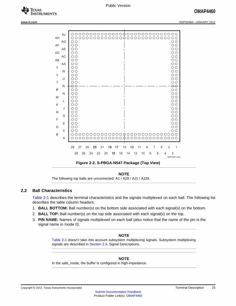
SWPS041-004
AJ
AG
AH
AE
AF
AD
AC
AB
AA
Y
W
V
U
T
R
P
N
P
M
L
K
J
H
G
H
E
H
F
D
B
C
A
29 27
28
25
26
23
24
23
22
23 21
20 18
19
18 16
19 1717 15 13
14 12
13 11
10
9
8
7
6
5
4
3 1
2
Public Version
OMAP4460
www.ti.com SWPS046A –JANUARY 2012
Figure 2-2. S-PBGA-N547 Package (Top View)
NOTEThe following top balls are unconnected: A1 / A29 / AJ1 / AJ29.
2.2 Ball Characteristics
Table 2-1 describes the terminal characteristics and the signals multiplexed on each ball. The following listdescribes the table column headers:
1. BALL BOTTOM: Ball number(s) on the bottom side associated with each signal(s) on the bottom.
2. BALL TOP: Ball number(s) on the top side associated with each signal(s) on the top.
3. PIN NAME: Names of signals multiplexed on each ball (also notice that the name of the pin is thesignal name in mode 0).
NOTETable 2-1 doesn’t take into account subsystem multiplexing signals. Subsystem multiplexingsignals are described in Section 2.4, Signal Descriptions.
NOTEIn the safe_mode, the buffer is configured in high-impedance.
Copyright © 2012, Texas Instruments Incorporated Terminal Description 25Submit Documentation Feedback
Product Folder Link(s): OMAP4460
Public Version
OMAP4460
SWPS046A –JANUARY 2012 www.ti.com
4. MODE: Multiplexing mode number:
(a) Mode 0 is the primary mode; this means that when mode 0 is set, the function mapped on the pincorresponds to the name of the pin. There is always a function mapped on the primary mode. Notethat the primary mode is not necessarily the default mode.
NOTEThe default mode is the mode at the release of the reset; also see the RESET REL.MODE column.
(b) Modes 1 to 7 are possible modes for alternate functions. On each pin, some modes are effectivelyused for alternate functions, while some modes are not used and correspond to a safe mode perdesign implementation.
5. TYPE: Signal type and direction:
– I = Input– O = Output– I/O = Input/Output– D = Open drain– DS = Differential– A = Analog– PWR = Power– GND = Ground
6. BALL RESET STATE: The state of the terminal at power-on reset:
– 0: The buffer drives VOL (pulldown/pullup resistor not activated)– 0(PD): The buffer drives VOL with an active pulldown resistor.– 1: The buffer drives VOH (pulldown/pullup resistor not activated)– 1(PU): The buffer drives VOH with an active pullup resistor.– Z: High-impedance– L: High-impedance with an active pulldown resistor– H: High-impedance with an active pullup resistor
7. BALL RESET REL. STATE: The state of the terminal at the release of the System Control Modulereset (PRCM CORE_PWRON_RET_RST reset signal).
– 0: The buffer drives VOL (pulldown/pullup resistor not activated)– 0(PD): The buffer drives VOL with an active pulldown resistor.– 1: The buffer drives VOH (pulldown/pullup resistor not activated)– 1(PU): The buffer drives VOH with an active pullup resistor.– Z: High-impedance– L: High-impedance with an active pulldown resistor– H: High-impedance with an active pullup resistor
NOTEFor more information on the CORE_PWRON_RET_RST reset signal and its reset sources,see the Power Reset and Clock Management / PRCM Reset Management FunctionalDescription section of the OMAP4460 TRM.
8. RESET REL. MODE: This mode is automatically configured at the release of the System ControlModule reset (PRCM CORE_PWRON_RET_RST reset signal).
NOTEFor more information on the CORE_PWRON_RET_RST reset signal and its reset sources,see the Power Reset and Clock Management / PRCM Reset Management FunctionalDescription section of the OMAP4460 TRM.
26 Terminal Description Copyright © 2012, Texas Instruments Incorporated
Submit Documentation FeedbackProduct Folder Link(s): OMAP4460
Public Version
OMAP4460
www.ti.com SWPS046A –JANUARY 2012
9. POWER: The voltage supply that powers the terminal I/O buffers.
10. HYS: Indicates if the input buffer is with hysteresis:
– Yes: With high hysteresis– No: Without low hysteresis
NOTEThe hysteresis value is equal to minimum 150 mV for 1.8 V, or minimum 135 mV for 1.2 V,unless otherwise specified. For more information, see the hysteresis values in Section 3.3,DC Electrical Characteristics.
11. BUFFER STRENGTH: Drive strength of the associated output buffer.
NOTEFor programmable buffer strength:– The default value is given in Table 2-1– A note describes all possible values according to the selected mode.– The pin is assured to supply up to this amount in steady-state.
12. PULL U/D – TYPE: Denotes the presence of an internal pullup or pulldown resistor. Pullup andpulldown resistors can be enabled or disabled via software.
NOTEThe pullup/pulldown drive strength is equal to: minimum = 50 μA, typical = 100 μA, maximum= 250 μA, unless otherwise specified.
13. IO CELL: IO cell information:
– LVCMOS: The IO buffer receives or drives a standard GPIO signal.– Open Drain: The IO buffer outputs an open drain signal.– PHY: This is for MIPI D-PHY signals.– Analog: For Analog signals– SubLVDS: The IO buffer supports the differential mode.– Dual Voltage: The IO buffer is designed to support two voltages (for instance, 1.2V and 1.8V, or
1.8V and 3.0V).
NOTEConfiguring two pins to the same input signal is not supported as it can yield unexpectedresults. This can be easily prevented with the proper software configuration. (safe_mode isnot an input signal.)
NOTEWhen a pad is set into a multiplexing mode which is not defined by pin multiplexing, this padis actually set undriven (HiZ) with potential pullup/pulldown. Pulls need to be disabled tohave a pure HiZ.
NOTEAll balls not described in Table 2-1 are not connected.
Copyright © 2012, Texas Instruments Incorporated Terminal Description 27Submit Documentation Feedback
Product Folder Link(s): OMAP4460
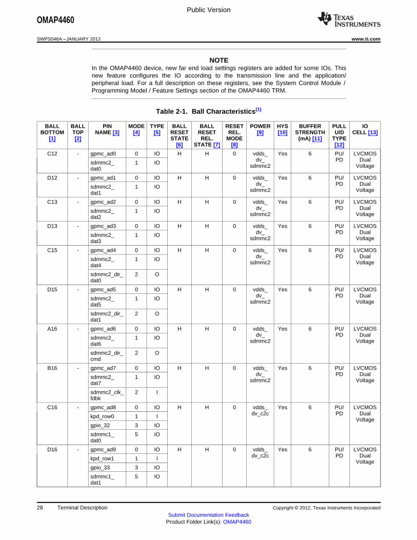
Public Version
OMAP4460
SWPS046A –JANUARY 2012 www.ti.com
NOTEIn the OMAP4460 device, new far end load settings registers are added for some IOs. Thisnew feature configures the IO according to the transmission line and the application/peripheral load. For a full description on these registers, see the System Control Module /Programming Model / Feature Settings section of the OMAP4460 TRM.
Table 2-1. Ball Characteristics(1)
BALL BALL PIN MODE TYPE BALL BALL RESET POWER HYS BUFFER PULL IOBOTTOM TOP NAME [3] [4] [5] RESET RESET REL. [9] [10] STRENGTH U/D CELL [13]
[1] [2] STATE REL. MODE (mA) [11] TYPE[6] STATE [7] [8] [12]
C12 - gpmc_ad0 0 IO H H 0 vdds_ Yes 6 PU/ LVCMOSdv_ PD Dualsdmmc2_ 1 IO
sdmmc2 Voltagedat0
D12 - gpmc_ad1 0 IO H H 0 vdds_ Yes 6 PU/ LVCMOSdv_ PD Dualsdmmc2_ 1 IO
sdmmc2 Voltagedat1
C13 - gpmc_ad2 0 IO H H 0 vdds_ Yes 6 PU/ LVCMOSdv_ PD Dualsdmmc2_ 1 IO
sdmmc2 Voltagedat2
D13 - gpmc_ad3 0 IO H H 0 vdds_ Yes 6 PU/ LVCMOSdv_ PD Dualsdmmc2_ 1 IO
sdmmc2 Voltagedat3
C15 - gpmc_ad4 0 IO H H 0 vdds_ Yes 6 PU/ LVCMOSdv_ PD Dualsdmmc2_ 1 IO
sdmmc2 Voltagedat4
sdmmc2_dir_ 2 Odat0
D15 - gpmc_ad5 0 IO H H 0 vdds_ Yes 6 PU/ LVCMOSdv_ PD Dualsdmmc2_ 1 IO
sdmmc2 Voltagedat5
sdmmc2_dir_ 2 Odat1
A16 - gpmc_ad6 0 IO H H 0 vdds_ Yes 6 PU/ LVCMOSdv_ PD Dualsdmmc2_ 1 IO
sdmmc2 Voltagedat6
sdmmc2_dir_ 2 Ocmd
B16 - gpmc_ad7 0 IO H H 0 vdds_ Yes 6 PU/ LVCMOSdv_ PD Dualsdmmc2_ 1 IO
sdmmc2 Voltagedat7
sdmmc2_clk_ 2 Ifdbk
C16 - gpmc_ad8 0 IO H H 0 vdds_ Yes 6 PU/ LVCMOSdv_c2c PD Dualkpd_row0 1 I
Voltagegpio_32 3 IO
sdmmc1_ 5 IOdat0
D16 - gpmc_ad9 0 IO H H 0 vdds_ Yes 6 PU/ LVCMOSdv_c2c PD Dualkpd_row1 1 I
Voltagegpio_33 3 IO
sdmmc1_ 5 IOdat1
28 Terminal Description Copyright © 2012, Texas Instruments Incorporated
Submit Documentation FeedbackProduct Folder Link(s): OMAP4460
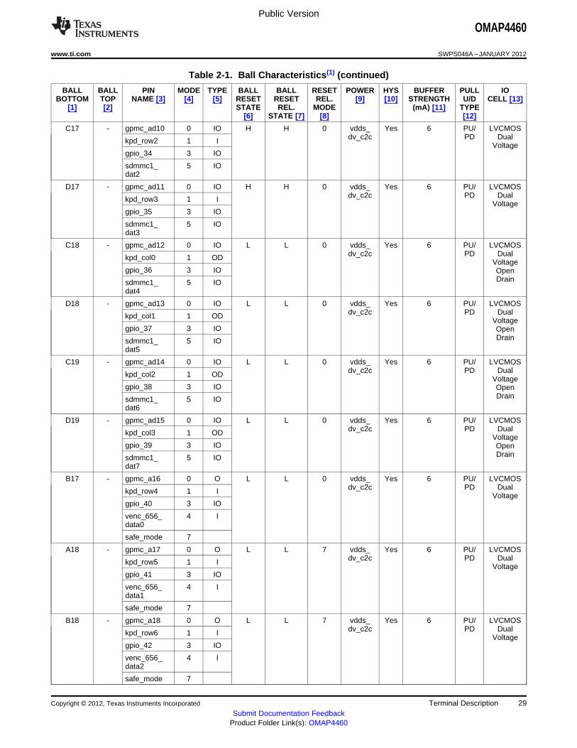
Public Version
OMAP4460
www.ti.com SWPS046A –JANUARY 2012
Table 2-1. Ball Characteristics(1) (continued)
BALL BALL PIN MODE TYPE BALL BALL RESET POWER HYS BUFFER PULL IOBOTTOM TOP NAME [3] [4] [5] RESET RESET REL. [9] [10] STRENGTH U/D CELL [13]
[1] [2] STATE REL. MODE (mA) [11] TYPE[6] STATE [7] [8] [12]
C17 - gpmc_ad10 0 IO H H 0 vdds_ Yes 6 PU/ LVCMOSdv_c2c PD Dualkpd_row2 1 I
Voltagegpio_34 3 IO
sdmmc1_ 5 IOdat2
D17 - gpmc_ad11 0 IO H H 0 vdds_ Yes 6 PU/ LVCMOSdv_c2c PD Dualkpd_row3 1 I
Voltagegpio_35 3 IO
sdmmc1_ 5 IOdat3
C18 - gpmc_ad12 0 IO L L 0 vdds_ Yes 6 PU/ LVCMOSdv_c2c PD Dualkpd_col0 1 OD
Voltagegpio_36 3 IO Open
Drainsdmmc1_ 5 IOdat4
D18 - gpmc_ad13 0 IO L L 0 vdds_ Yes 6 PU/ LVCMOSdv_c2c PD Dualkpd_col1 1 OD
Voltagegpio_37 3 IO Open
Drainsdmmc1_ 5 IOdat5
C19 - gpmc_ad14 0 IO L L 0 vdds_ Yes 6 PU/ LVCMOSdv_c2c PD Dualkpd_col2 1 OD
Voltagegpio_38 3 IO Open
Drainsdmmc1_ 5 IOdat6
D19 - gpmc_ad15 0 IO L L 0 vdds_ Yes 6 PU/ LVCMOSdv_c2c PD Dualkpd_col3 1 OD
Voltagegpio_39 3 IO Open
Drainsdmmc1_ 5 IOdat7
B17 - gpmc_a16 0 O L L 0 vdds_ Yes 6 PU/ LVCMOSdv_c2c PD Dualkpd_row4 1 I
Voltagegpio_40 3 IO
venc_656_ 4 Idata0
safe_mode 7
A18 - gpmc_a17 0 O L L 7 vdds_ Yes 6 PU/ LVCMOSdv_c2c PD Dualkpd_row5 1 I
Voltagegpio_41 3 IO
venc_656_ 4 Idata1
safe_mode 7
B18 - gpmc_a18 0 O L L 7 vdds_ Yes 6 PU/ LVCMOSdv_c2c PD Dualkpd_row6 1 I
Voltagegpio_42 3 IO
venc_656_ 4 Idata2
safe_mode 7
Copyright © 2012, Texas Instruments Incorporated Terminal Description 29Submit Documentation Feedback
Product Folder Link(s): OMAP4460

Public Version
OMAP4460
SWPS046A –JANUARY 2012 www.ti.com
Table 2-1. Ball Characteristics(1) (continued)
BALL BALL PIN MODE TYPE BALL BALL RESET POWER HYS BUFFER PULL IOBOTTOM TOP NAME [3] [4] [5] RESET RESET REL. [9] [10] STRENGTH U/D CELL [13]
[1] [2] STATE REL. MODE (mA) [11] TYPE[6] STATE [7] [8] [12]
A19 - gpmc_a19 0 O L L 7 vdds_ Yes 6 PU/ LVCMOSdv_c2c PD Dualkpd_row7 1 I
Voltagegpio_43 3 IO
venc_656_ 4 Idata3
safe_mode 7
B19 - gpmc_a20 0 O H L 7 vdds_ Yes 6 PU/ LVCMOSdv_c2c PD Dualkpd_col4 1 OD
Voltagegpio_44 3 IO Open
Drainvenc_656_ 4 Idata4
safe_mode 7
B20 - gpmc_a21 0 O H L 7 vdds_ Yes 6 PU/ LVCMOSdv_c2c PD Dualkpd_col5 1 OD
Voltagegpio_45 3 IO Open
Drainvenc_656_ 4 Idata5
safe_mode 7
A21 - gpmc_a22 0 O H L 7 vdds_ Yes 6 PU/ LVCMOSdv_c2c PD Dualkpd_col6 1 OD
Voltagegpio_46 3 IO Open
Drainvenc_656_ 4 Idata6
safe_mode 7
B21 - gpmc_a23 0 O H L 7 vdds_ Yes 6 PU/ LVCMOSdv_c2c PD Dualkpd_col7 1 OD
Voltagegpio_47 3 IO Open
Drainvenc_656_ 4 Idata7
safe_mode 7
C20 - gpmc_a24 0 O H L 7 vdds_ Yes 6 PU/ LVCMOSdv_c2c PD Dualkpd_col8 1 OD
Voltagegpio_48 3 IO Open
Drainsafe_mode 7
D20 - gpmc_a25 0 O H L 7 vdds_ Yes 6 PU/ LVCMOSdv_c2c PD Dualgpio_49 3 IO
Voltagesafe_mode 7
B25 - gpmc_ncs0 0 O H 1 0 vdds_ Yes 6 PU/ LVCMOSdv_ PD Dualgpio_50 3 IO
gpmc Voltagesys_ 4 Indmareq0
C21 - gpmc_ncs1 0 O H H 7 vdds_ Yes 6 PU/ LVCMOSdv_c2c PD Dualgpio_51 3 IO
Voltagesafe_mode 7
30 Terminal Description Copyright © 2012, Texas Instruments Incorporated
Submit Documentation FeedbackProduct Folder Link(s): OMAP4460
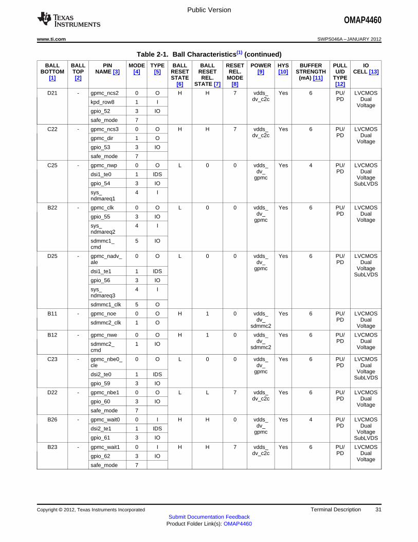
Public Version
OMAP4460
www.ti.com SWPS046A –JANUARY 2012
Table 2-1. Ball Characteristics(1) (continued)
BALL BALL PIN MODE TYPE BALL BALL RESET POWER HYS BUFFER PULL IOBOTTOM TOP NAME [3] [4] [5] RESET RESET REL. [9] [10] STRENGTH U/D CELL [13]
[1] [2] STATE REL. MODE (mA) [11] TYPE[6] STATE [7] [8] [12]
D21 - gpmc_ncs2 0 O H H 7 vdds_ Yes 6 PU/ LVCMOSdv_c2c PD Dualkpd_row8 1 I
Voltagegpio_52 3 IO
safe_mode 7
C22 - gpmc_ncs3 0 O H H 7 vdds_ Yes 6 PU/ LVCMOSdv_c2c PD Dualgpmc_dir 1 O
Voltagegpio_53 3 IO
safe_mode 7
C25 - gpmc_nwp 0 O L 0 0 vdds_ Yes 4 PU/ LVCMOSdv_ PD Dualdsi1_te0 1 IDS
gpmc Voltagegpio_54 3 IO SubLVDS
sys_ 4 Indmareq1
B22 - gpmc_clk 0 O L 0 0 vdds_ Yes 6 PU/ LVCMOSdv_ PD Dualgpio_55 3 IO
gpmc Voltagesys_ 4 Indmareq2
sdmmc1_ 5 IOcmd
D25 - gpmc_nadv_ 0 O L 0 0 vdds_ Yes 6 PU/ LVCMOSale dv_ PD Dual
gpmc Voltagedsi1_te1 1 IDSSubLVDS
gpio_56 3 IO
sys_ 4 Indmareq3
sdmmc1_clk 5 O
B11 - gpmc_noe 0 O H 1 0 vdds_ Yes 6 PU/ LVCMOSdv_ PD Dualsdmmc2_clk 1 O
sdmmc2 Voltage
B12 - gpmc_nwe 0 O H 1 0 vdds_ Yes 6 PU/ LVCMOSdv_ PD Dualsdmmc2_ 1 IO
sdmmc2 Voltagecmd
C23 - gpmc_nbe0_ 0 O L 0 0 vdds_ Yes 6 PU/ LVCMOScle dv_ PD Dual
gpmc Voltagedsi2_te0 1 IDSSubLVDS
gpio_59 3 IO
D22 - gpmc_nbe1 0 O L L 7 vdds_ Yes 6 PU/ LVCMOSdv_c2c PD Dualgpio_60 3 IO
Voltagesafe_mode 7
B26 - gpmc_wait0 0 I H H 0 vdds_ Yes 4 PU/ LVCMOSdv_ PD Dualdsi2_te1 1 IDS
gpmc Voltagegpio_61 3 IO SubLVDS
B23 - gpmc_wait1 0 I H H 7 vdds_ Yes 6 PU/ LVCMOSdv_c2c PD Dualgpio_62 3 IO
Voltagesafe_mode 7
Copyright © 2012, Texas Instruments Incorporated Terminal Description 31Submit Documentation Feedback
Product Folder Link(s): OMAP4460

Public Version
OMAP4460
SWPS046A –JANUARY 2012 www.ti.com
Table 2-1. Ball Characteristics(1) (continued)
BALL BALL PIN MODE TYPE BALL BALL RESET POWER HYS BUFFER PULL IOBOTTOM TOP NAME [3] [4] [5] RESET RESET REL. [9] [10] STRENGTH U/D CELL [13]
[1] [2] STATE REL. MODE (mA) [11] TYPE[6] STATE [7] [8] [12]
D23 - gpmc_wait2 0 I L L 7 vdds_ Yes 6 PU/ LVCMOSdv_c2c PD Dualusbc1_icusb_ 1 O
Voltagetxen
gpio_100 3 IO
sys_ 4 Indmareq0
safe_mode 7
A24 - gpmc_ncs4 0 O L L 7 vdds_ Yes 6 PU/ LVCMOSdv_c2c PD Dualdsi1_te0 1 IDS
Voltagegpio_101 3 IO SubLVDS
sys_ 4 Indmareq1
safe_mode 7
B24 - gpmc_ncs5 0 O L L 7 vdds_ Yes 6 PU/ LVCMOSdv_c2c PD Dualdsi1_te1 1 IDS
Voltagegpio_102 3 IO SubLVDS
sys_ 4 Indmareq2
safe_mode 7
C24 - gpmc_ncs6 0 O L L 7 vdds_ Yes 6 PU/ LVCMOSdv_c2c PD Dualdsi2_te0 1 IDS
Voltagegpio_103 3 IO SubLVDS
sys_ 4 Indmareq3
safe_mode 7
D24 - gpmc_ncs7 0 O L L 7 vdds_ Yes 6 PU/ LVCMOSdv_c2c PD Dualdsi2_te1 1 IDS
Voltagegpio_104 3 IO SubLVDS
safe_mode 7
- E29 lpddr21_dq0 0 IO L L 0 vddq_ NA 0.1 PUy/ LVCMOSlpddr2 PDy(2)
- D28 lpddr21_dq1 0 IO L L 0 vddq_ NA 0.1 PUy/ LVCMOSlpddr2 PDy(2)
- B27 lpddr21_dq2 0 IO L L 0 vddq_ NA 0.1 PUy/ LVCMOSlpddr2 PDy(2)
- A27 lpddr21_dq3 0 IO L L 0 vddq_ NA 0.1 PUy/ LVCMOSlpddr2 PDy(2)
- A26 lpddr21_dq4 0 IO L L 0 vddq_ NA 0.1 PUy/ LVCMOSlpddr2 PDy(2)
- B26 lpddr21_dq5 0 IO L L 0 vddq_ NA 0.1 PUy/ LVCMOSlpddr2 PDy(2)
- A25 lpddr21_dq6 0 IO L L 0 vddq_ NA 0.1 PUy/ LVCMOSlpddr2 PDy(2)
- A24 lpddr21_dq7 0 IO L L 0 vddq_ NA 0.1 PUy/ LVCMOSlpddr2 PDy(2)
- B19 lpddr21_dq8 0 IO L L 0 vddq_ NA 0.1 PUy/ LVCMOSlpddr2 PDy(2)
- A19 lpddr21_dq9 0 IO L L 0 vddq_ NA 0.1 PUy/ LVCMOSlpddr2 PDy(2)
32 Terminal Description Copyright © 2012, Texas Instruments Incorporated
Submit Documentation FeedbackProduct Folder Link(s): OMAP4460

Public Version
OMAP4460
www.ti.com SWPS046A –JANUARY 2012
Table 2-1. Ball Characteristics(1) (continued)
BALL BALL PIN MODE TYPE BALL BALL RESET POWER HYS BUFFER PULL IOBOTTOM TOP NAME [3] [4] [5] RESET RESET REL. [9] [10] STRENGTH U/D CELL [13]
[1] [2] STATE REL. MODE (mA) [11] TYPE[6] STATE [7] [8] [12]
- A18 lpddr21_dq10 0 IO L L 0 vddq_ NA 0.1 PUy/ LVCMOSlpddr2 PDy(2)
- A17 lpddr21_dq11 0 IO L L 0 vddq_ NA 0.1 PUy/ LVCMOSlpddr2 PDy(2)
- B17 lpddr21_dq12 0 IO L L 0 vddq_ NA 0.1 PUy/ LVCMOSlpddr2 PDy(2)
- A13 lpddr21_dq13 0 IO L L 0 vddq_ NA 0.1 PUy/ LVCMOSlpddr2 PDy(2)
- A12 lpddr21_dq14 0 IO L L 0 vddq_ NA 0.1 PUy/ LVCMOSlpddr2 PDy(2)
- B12 lpddr21_dq15 0 IO L L 0 vddq_ NA 0.1 PUy/ LVCMOSlpddr2 PDy(2)
- N28 lpddr21_dq16 0 IO L L 0 vddq_ NA 0.1 PUy/ LVCMOSlpddr2 PDy(2)
- N29 lpddr21_dq17 0 IO L L 0 vddq_ NA 0.1 PUy/ LVCMOSlpddr2 PDy(2)
- M29 lpddr21_dq18 0 IO L L 0 vddq_ NA 0.1 PUy/ LVCMOSlpddr2 PDy(2)
- L28 lpddr21_dq19 0 IO L L 0 vddq_ NA 0.1 PUy/ LVCMOSlpddr2 PDy(2)
- K28 lpddr21_dq20 0 IO L L 0 vddq_ NA 0.1 PUy/ LVCMOSlpddr2 PDy(2)
- K29 lpddr21_dq21 0 IO L L 0 vddq_ NA 0.1 PUy/ LVCMOSlpddr2 PDy(2)
- J29 lpddr21_dq22 0 IO L L 0 vddq_ NA 0.1 PUy/ LVCMOSlpddr2 PDy(2)
- H29 lpddr21_dq23 0 IO L L 0 vddq_ NA 0.1 PUy/ LVCMOSlpddr2 PDy(2)
- B8 lpddr21_dq24 0 IO L L 0 vddq_ NA 0.1 PUy/ LVCMOSlpddr2 PDy(2)
- A8 lpddr21_dq25 0 IO L L 0 vddq_ NA 0.1 PUy/ LVCMOSlpddr2 PDy(2)
- A7 lpddr21_dq26 0 IO L L 0 vddq_ NA 0.1 PUy/ LVCMOSlpddr2 PDy(2)
- B6 lpddr21_dq27 0 IO L L 0 vddq_ NA 0.1 PUy/ LVCMOSlpddr2 PDy(2)
- B5 lpddr21_dq28 0 IO L L 0 vddq_ NA 0.1 PUy/ LVCMOSlpddr2 PDy(2)
- A5 lpddr21_dq29 0 IO L L 0 vddq_ N A 0.1 PUy/ LVCMOSlpddr2 PDy(2)
- A4 lpddr21_dq30 0 IO L L 0 vddq_ NA 0.1 PUy/ LVCMOSlpddr2 PDy(2)
- B3 lpddr21_dq31 0 IO L L 0 vddq_ NA 0.1 PUy/ LVCMOSlpddr2 PDy(2)
- AJ27 lpddr21_ca0 0 O L L 0 vddca_ NA 0.1 PUy/ LVCMOSlpddr21 PDy(2)
- AH27 lpddr21_ca1 0 O L L 0 vddca_ NA 0.1 PUy/ LVCMOSlpddr21 PDy(2)
- AH26 lpddr21_ca2 0 O L L 0 vddca_ NA 0.1 PUy/ LVCMOSlpddr21 PDy(2)
- AH25 lpddr21_ca3 0 O L L 0 vddca_ NA 0.1 PUy/ LVCMOSlpddr21 PDy(2)
- AJ25 lpddr21_ca4 0 O L L 0 vddca_ NA 0.1 PUy/ LVCMOSlpddr21 PDy(2)
Copyright © 2012, Texas Instruments Incorporated Terminal Description 33Submit Documentation Feedback
Product Folder Link(s): OMAP4460
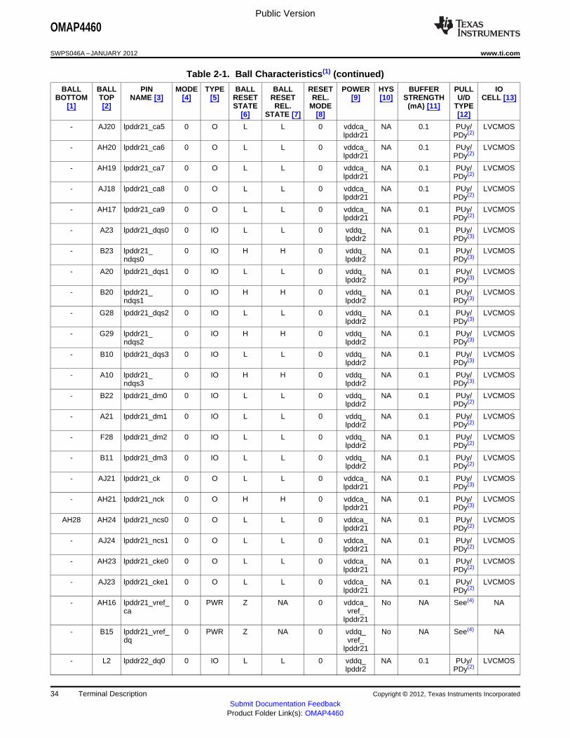
Public Version
OMAP4460
SWPS046A –JANUARY 2012 www.ti.com
Table 2-1. Ball Characteristics(1) (continued)
BALL BALL PIN MODE TYPE BALL BALL RESET POWER HYS BUFFER PULL IOBOTTOM TOP NAME [3] [4] [5] RESET RESET REL. [9] [10] STRENGTH U/D CELL [13]
[1] [2] STATE REL. MODE (mA) [11] TYPE[6] STATE [7] [8] [12]
- AJ20 lpddr21_ca5 0 O L L 0 vddca_ NA 0.1 PUy/ LVCMOSlpddr21 PDy(2)
- AH20 lpddr21_ca6 0 O L L 0 vddca_ NA 0.1 PUy/ LVCMOSlpddr21 PDy(2)
- AH19 lpddr21_ca7 0 O L L 0 vddca_ NA 0.1 PUy/ LVCMOSlpddr21 PDy(2)
- AJ18 lpddr21_ca8 0 O L L 0 vddca_ NA 0.1 PUy/ LVCMOSlpddr21 PDy(2)
- AH17 lpddr21_ca9 0 O L L 0 vddca_ NA 0.1 PUy/ LVCMOSlpddr21 PDy(2)
- A23 lpddr21_dqs0 0 IO L L 0 vddq_ NA 0.1 PUy/ LVCMOSlpddr2 PDy(3)
- B23 lpddr21_ 0 IO H H 0 vddq_ NA 0.1 PUy/ LVCMOSndqs0 lpddr2 PDy(3)
- A20 lpddr21_dqs1 0 IO L L 0 vddq_ NA 0.1 PUy/ LVCMOSlpddr2 PDy(3)
- B20 lpddr21_ 0 IO H H 0 vddq_ NA 0.1 PUy/ LVCMOSndqs1 lpddr2 PDy(3)
- G28 lpddr21_dqs2 0 IO L L 0 vddq_ NA 0.1 PUy/ LVCMOSlpddr2 PDy(3)
- G29 lpddr21_ 0 IO H H 0 vddq_ NA 0.1 PUy/ LVCMOSndqs2 lpddr2 PDy(3)
- B10 lpddr21_dqs3 0 IO L L 0 vddq_ NA 0.1 PUy/ LVCMOSlpddr2 PDy(3)
- A10 lpddr21_ 0 IO H H 0 vddq_ NA 0.1 PUy/ LVCMOSndqs3 lpddr2 PDy(3)
- B22 lpddr21_dm0 0 IO L L 0 vddq_ NA 0.1 PUy/ LVCMOSlpddr2 PDy(2)
- A21 lpddr21_dm1 0 IO L L 0 vddq_ NA 0.1 PUy/ LVCMOSlpddr2 PDy(2)
- F28 lpddr21_dm2 0 IO L L 0 vddq_ NA 0.1 PUy/ LVCMOSlpddr2 PDy(2)
- B11 lpddr21_dm3 0 IO L L 0 vddq_ NA 0.1 PUy/ LVCMOSlpddr2 PDy(2)
- AJ21 lpddr21_ck 0 O L L 0 vddca_ NA 0.1 PUy/ LVCMOSlpddr21 PDy(3)
- AH21 lpddr21_nck 0 O H H 0 vddca_ NA 0.1 PUy/ LVCMOSlpddr21 PDy(3)
AH28 AH24 lpddr21_ncs0 0 O L L 0 vddca_ NA 0.1 PUy/ LVCMOSlpddr21 PDy(2)
- AJ24 lpddr21_ncs1 0 O L L 0 vddca_ NA 0.1 PUy/ LVCMOSlpddr21 PDy(2)
- AH23 lpddr21_cke0 0 O L L 0 vddca_ NA 0.1 PUy/ LVCMOSlpddr21 PDy(2)
- AJ23 lpddr21_cke1 0 O L L 0 vddca_ NA 0.1 PUy/ LVCMOSlpddr21 PDy(2)
- AH16 lpddr21_vref_ 0 PWR Z NA 0 vddca_ No NA See(4) NAca vref_
lpddr21
- B15 lpddr21_vref_ 0 PWR Z NA 0 vddq_ No NA See(4) NAdq vref_
lpddr21
- L2 lpddr22_dq0 0 IO L L 0 vddq_ NA 0.1 PUy/ LVCMOSlpddr2 PDy(2)
34 Terminal Description Copyright © 2012, Texas Instruments Incorporated
Submit Documentation FeedbackProduct Folder Link(s): OMAP4460

Public Version
OMAP4460
www.ti.com SWPS046A –JANUARY 2012
Table 2-1. Ball Characteristics(1) (continued)
BALL BALL PIN MODE TYPE BALL BALL RESET POWER HYS BUFFER PULL IOBOTTOM TOP NAME [3] [4] [5] RESET RESET REL. [9] [10] STRENGTH U/D CELL [13]
[1] [2] STATE REL. MODE (mA) [11] TYPE[6] STATE [7] [8] [12]
- M1 lpddr22_dq1 0 IO L L 0 vddq_ NA 0.1 PUy/ LVCMOSlpddr2 PDy(2)
- N1 lpddr22_dq2 0 IO L L 0 vddq_ NA 0.1 PUy/ LVCMOSlpddr2 PDy(2)
- U2 lpddr22_dq3 0 IO L L 0 vddq_ NA 0.1 PUy/ LVCMOSlpddr2 PDy(2)
- V1 lpddr22_dq4 0 IO L L 0 vddq_ NA 0.1 PUy/ LVCMOSlpddr2 PDy(2)
- W2 lpddr22_dq5 0 IO L L 0 vddq_ NA 0.1 PUy/ LVCMOSlpddr2 PDy(2)
- W1 lpddr22_dq6 0 IO L L 0 vddq_ NA 0.1 PUy/ LVCMOSlpddr2 PDy(2)
- Y2 lpddr22_dq7 0 IO L L 0 vddq_ NA 0.1 PUy/ LVCMOSlpddr2 PDy(2)
- AE1 lpddr22_dq8 0 IO L L 0 vddq_ NA 0.1 PUy/ LVCMOSlpddr2 PDy(2)
- AF1 lpddr22_dq9 0 IO L L 0 vddq_ NA 0.1 PUy/ LVCMOSlpddr2 PDy(2)
- AG1 lpddr22_dq10 0 IO L L 0 vddq_ NA 0.1 PUy/ LVCMOSlpddr2 PDy(2)
- AG2 lpddr22_dq11 0 IO L L 0 vddq_ NA 0.1 PUy/ LVCMOSlpddr2 PDy(2)
- AJ3 lpddr22_dq12 0 IO L L 0 vddq_ NA 0.1 PUy/ LVCMOSlpddr2 PDy(2)
- AH4 lpddr22_dq13 0 IO L L 0 vddq_ NA 0.1 PUy/ LVCMOSlpddr2 PDy(2)
- AJ5 lpddr22_dq14 0 IO L L 0 vddq_ NA 0.1 PUy/ LVCMOSlpddr2 PDy(2)
- AH6 lpddr22_dq15 0 IO L L 0 vddq_ NA 0.1 PUy/ LVCMOSlpddr2 PDy(2)
- C2 lpddr22_dq16 0 IO L L 0 vddq_ NA 0.1 PUy/ LVCMOSlpddr2 PDy(2)
- D1 lpddr22_dq17 0 IO L L 0 vddq_ NA 0.1 PUy/ LVCMOSlpddr2 PDy(2)
- E1 lpddr22_dq18 0 IO L L 0 vddq_ NA 0.1 PUy/ LVCMOSlpddr2 PDy(2)
- E2 lpddr22_dq19 0 IO L L 0 vddq_ NA 0.1 PUy/ LVCMOSlpddr2 PDy(2)
- F2 lpddr22_dq20 0 IO L L 0 vddq_ NA 0.1 PUy/ LVCMOSlpddr2 PDy(2)
- G1 lpddr22_dq21 0 IO L L 0 vddq_ NA 0.1 PUy/ LVCMOSlpddr2 PDy(2)
- H1 lpddr22_dq22 0 IO L L 0 vddq_ NA 0.1 PUy/ LVCMOSlpddr2 PDy(2)
- H2 lpddr22_dq23 0 IO L L 0 vddq_ NA 0.1 PUy/ LVCMOSlpddr2 PDy(2)
- AJ9 lpddr22_dq24 0 IO L L 0 vddq_ NA 0.1 PUy/ LVCMOSlpddr2 PDy(2)
- AJ10 lpddr22_dq25 0 IO L L 0 vddq_ NA 0.1 PUy/ LVCMOSlpddr2 PDy(2)
- AH10 lpddr22_dq26 0 IO L L 0 vddq_ NA 0.1 PUy/ LVCMOSlpddr2 PDy(2)
- AH11 lpddr22_dq27 0 IO L L 0 vddq_ NA 0.1 PUy/ LVCMOSlpddr2 PDy(2)
Copyright © 2012, Texas Instruments Incorporated Terminal Description 35Submit Documentation Feedback
Product Folder Link(s): OMAP4460

Public Version
OMAP4460
SWPS046A –JANUARY 2012 www.ti.com
Table 2-1. Ball Characteristics(1) (continued)
BALL BALL PIN MODE TYPE BALL BALL RESET POWER HYS BUFFER PULL IOBOTTOM TOP NAME [3] [4] [5] RESET RESET REL. [9] [10] STRENGTH U/D CELL [13]
[1] [2] STATE REL. MODE (mA) [11] TYPE[6] STATE [7] [8] [12]
- AJ12 lpddr22_dq28 0 IO L L 0 vddq_ NA 0.1 PUy/ LVCMOSlpddr2 PDy(2)
- AJ13 lpddr22_dq29 0 IO L L 0 vddq_ NA 0.1 PUy/ LVCMOSlpddr2 PDy(2)
- AH13 lpddr22_dq30 0 IO L L 0 vddq_ NA 0.1 PUy/ LVCMOSlpddr2 PDy(2)
- AJ14 lpddr22_dq31 0 IO L L 0 vddq_ NA 0.1 PUy/ LVCMOSlpddr2 PDy(2)
- R29 lpddr22_ca0 0 O L L 0 vddca_ NA 0.1 PUy/ LVCMOSlpddr22 PDy(2)
- T29 lpddr22_ca1 0 O L L 0 vddca_ NA 0.1 PUy/ LVCMOSlpddr22 PDy(2)
- U29 lpddr22_ca2 0 O L L 0 vddca_ NA 0.1 PUy/ LVCMOSlpddr22 PDy(2)
- V29 lpddr22_ca3 0 O L L 0 vddca_ NA 0.1 PUy/ LVCMOSlpddr22 PDy(2)
- W28 lpddr22_ca4 0 O L L 0 vddca_ NA 0.1 PUy/ LVCMOSlpddr22 PDy(2)
- AC29 lpddr22_ca5 0 O L L 0 vddca_ NA 0.1 PUy/ LVCMOSlpddr22 PDy(2)
- AD29 lpddr22_ca6 0 O L L 0 vddca_ NA 0.1 PUy/ LVCMOSlpddr22 PDy(2)
- AD28 lpddr22_ca7 0 O L L 0 vddca_ NA 0.1 PUy/ LVCMOSlpddr22 PDy(2)
- AE28 lpddr22_ca8 0 O L L 0 vddca_ NA 0.1 PUy/ LVCMOSlpddr22 PDy(2)
- AF29 lpddr22_ca9 0 O L L 0 vddca_ NA 0.1 PUy/ LVCMOSlpddr22 PDy(2)
- AA1 lpddr22_dqs0 0 O L L 0 vddq_ NA 0.1 PUy/ LVCMOSlpddr2 PDy(3)
- AA2 lpddr22_ 0 O H H 0 vddq_ NA 0.1 PUy/ LVCMOSndqs0 lpddr2 PDy(3)
- AD2 lpddr22_dqs1 0 O L L 0 vddq_ NA 0.1 PUy/ LVCMOSlpddr2 PDy(3)
- AD1 lpddr22_ 0 O H H 0 vddq_ NA 0.1 PUy/ LVCMOSndqs1 lpddr2 PDy(3)
- K2 lpddr22_dqs2 0 O L L 0 vddq_ NA 0.1 PUy/ LVCMOSlpddr2 PDy(3)
- K1 lpddr22_ 0 O H H 0 vddq_ NA 0.1 PUy/ LVCMOSndqs2 lpddr2 PDy(3)
- AH8 lpddr22_dqs3 0 O L L 0 vddq_ NA 0.1 PUy/ LVCMOSlpddr2 PDy(3)
- AJ8 lpddr22_ 0 O H H 0 vddq_ NA 0.1 PUy/ LVCMOSndqs3 lpddr2 PDy(3)
- AB1 lpddr22_dm0 0 IO L L 0 vddq_ NA 0.1 PUy/ LVCMOSlpddr2 PDy(2)
- AC2 lpddr22_dm1 0 IO L L 0 vddq_ NA 0.1 PUy/ LVCMOSlpddr2 PDy(2)
- L1 lpddr22_dm2 0 IO L L 0 vddq_ NA 0.1 PUy/ LVCMOSlpddr2 PDy(2)
- AH7 lpddr22_dm3 0 IO L L 0 vddq_ NA 0.1 PUy/ LVCMOSlpddr2 PDy(2)
- AB28 lpddr22_ck 0 O L L 0 vddca_ NA 0.1 PUy/ LVCMOSlpddr22 PDy(3)
36 Terminal Description Copyright © 2012, Texas Instruments Incorporated
Submit Documentation FeedbackProduct Folder Link(s): OMAP4460
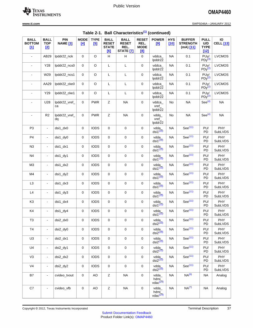
Public Version
OMAP4460
www.ti.com SWPS046A –JANUARY 2012
Table 2-1. Ball Characteristics(1) (continued)
BALL BALL PIN MODE TYPE BALL BALL RESET POWER HYS BUFFER PULL IOBOTTOM TOP NAME [3] [4] [5] RESET RESET REL. [9] [10] STRENGTH U/D CELL [13]
[1] [2] STATE REL. MODE (mA) [11] TYPE[6] STATE [7] [8] [12]
- AB29 lpddr22_nck 0 O H H 0 vddca_ NA 0.1 PUy/ LVCMOSlpddr22 PDy(3)
- Y28 lpddr22_ncs0 0 O L L 0 vddca_ NA 0.1 PUy/ LVCMOSlpddr22 PDy(2)
- W29 lpddr22_ncs1 0 O L L 0 vddca_ NA 0.1 PUy/ LVCMOSlpddr22 PDy(2)
- AA29 lpddr22_cke0 0 O L L 0 vddca_ NA 0.1 PUy/ LVCMOSlpddr22 PDy(2)
- Y29 lpddr22_cke1 0 O L L 0 vddca_ NA 0.1 PUy/ LVCMOSlpddr22 PDy(2)
- U28 lpddr22_vref_ 0 PWR Z NA 0 vddca_ No NA See(4) NAca vref_
lpddr22
- R2 lpddr22_vref_ 0 PWR Z NA 0 vddq_ No NA See(4) NAdq vref_
lpddr22
P3 - dsi1_dx0 0 IODS 0 0 0 vdda_ NA See(11) PU/ PHYdsi1(23) PD SubLVDS
P4 - dsi1_dy0 0 IODS 0 0 0 vdda_ NA See(11) PU/ PHYdsi1(23) PD SubLVDS
N3 - dsi1_dx1 0 IODS 0 0 0 vdda_ NA See(11) PU/ PHYdsi1(23) PD SubLVDS
N4 - dsi1_dy1 0 IODS 0 0 0 vdda_ NA See(11) PU/ PHYdsi1(23) PD SubLVDS
M3 - dsi1_dx2 0 IODS 0 0 0 vdda_ NA See(11) PU/ PHYdsi1(23) PD SubLVDS
M4 - dsi1_dy2 0 IODS 0 0 0 vdda_ NA See(11) PU/ PHYdsi1(23) PD SubLVDS
L3 - dsi1_dx3 0 IODS 0 0 0 vdda_ NA See(11) PU/ PHYdsi1(23) PD SubLVDS
L4 - dsi1_dy3 0 IODS 0 0 0 vdda_ NA See(11) PU/ PHYdsi1(23) PD SubLVDS
K3 - dsi1_dx4 0 IODS 0 0 0 vdda_ NA See(11) PU/ PHYdsi1(23) PD SubLVDS
K4 - dsi1_dy4 0 IODS 0 0 0 vdda_ NA See(11) PU/ PHYdsi1(23) PD SubLVDS
T3 - dsi2_dx0 0 IODS 0 0 0 vdda_ NA See(11) PU/ PHYdsi2(23) PD SubLVDS
T4 - dsi2_dy0 0 IODS 0 0 0 vdda_ NA See(11) PU/ PHYdsi2(23) PD SubLVDS
U3 - dsi2_dx1 0 IODS 0 0 0 vdda_ NA See(11) PU/ PHYdsi2(23) PD SubLVDS
U4 - dsi2_dy1 0 IODS 0 0 0 vdda_ NA See(11) PU/ PHYdsi2(23) PD SubLVDS
V3 - dsi2_dx2 0 IODS 0 0 0 vdda_ NA See(11) PU/ PHYdsi2(23) PD SubLVDS
V4 - dsi2_dy2 0 IODS 0 0 0 vdda_ NA See(11) PU/ PHYdsi2(23) PD SubLVDS
B7 - cvideo_tvout 0 AO Z NA 0 vdda_ NA NA(6) NA Analoghdmi_
vdac(24)
C7 - cvideo_vfb 0 AO Z NA 0 vdda_ NA NA(7) NA Analoghdmi_
vdac(24)
Copyright © 2012, Texas Instruments Incorporated Terminal Description 37Submit Documentation Feedback
Product Folder Link(s): OMAP4460

Public Version
OMAP4460
SWPS046A –JANUARY 2012 www.ti.com
Table 2-1. Ball Characteristics(1) (continued)
BALL BALL PIN MODE TYPE BALL BALL RESET POWER HYS BUFFER PULL IOBOTTOM TOP NAME [3] [4] [5] RESET RESET REL. [9] [10] STRENGTH U/D CELL [13]
[1] [2] STATE REL. MODE (mA) [11] TYPE[6] STATE [7] [8] [12]
D7 - cvideo_rset 0 AIO Z NA 0 vdda_ NA NA NA LVCMOShdmi_ Analog
vdac(24)
B9 - hdmi_hpd 0 I L L 7 vdds_ Yes 4 PU/ LVCMOS1p8v PDgpio_63 3 IO
safe_mode 7
B10 - hdmi_cec 0 IO H H 7 vdds_ Yes 4 PU/ LVCMOS1p8v PDgpio_64 3 IO
safe_mode 7
A8 - hdmi_ddc_scl 0 OD H H 7 vdds_ Yes 3 PUx/ LVCMOS1p8v PDy- Opengpio_65 3 IO 4
GPIO Drainsafe_mode 7 4
B8 - hdmi_ddc_ 0 IOD H H 7 vdds_ Yes 3 PUx/ LVCMOSsda 1p8v PDy- Open
GPIO Draingpio_66 3 IO 4
safe_mode 7 4
C8 - hdmi_data2x 0 ODS Z Z 0 vdda_ NA See(12) PD(30) PHY(29) hdmi_ SubLVDS
vdac(24) FS
D8 - hdmi_data2y 0 ODS Z Z 0 vdda_ NA See(12) PD(30) PHY(29) hdmi_ SubLVDS
vdac(24) FS
C9 - hdmi_data1x 0 ODS Z Z 0 vdda_ NA See(12) PD(30) PHY(29) hdmi_ SubLVDS
vdac(24) FS
D9 - hdmi_data1y 0 ODS Z Z 0 vdda_ NA See(12) PD(30) PHY(29) hdmi_ SubLVDS
vdac(24) FS
C10 - hdmi_data0x 0 ODS Z Z 0 vdda_ NA See(12) PD(30) PHY(29) hdmi_ SubLVDS
vdac(24) FS
D10 - hdmi_data0y 0 ODS Z Z 0 vdda_ NA See(12) PD(30) PHY(29) hdmi_ SubLVDS
vdac(24) FS
C11 - hdmi_clockx 0 ODS Z Z 0 vdda_ NA See(12) PD(30) PHY(29) hdmi_ SubLVDS
vdac(24) FS
D11 - hdmi_clocky 0 ODS Z Z 0 vdda_ NA See(12) PD(30) PHY(29) hdmi_ SubLVDS
vdac(24) FS
R26 - csi21_dx0 0 IDS L L 7 vdda_ Yes NA PU/ PHYcsi21(22) (18) PD SubLVDSgpi_67 3 I
LVCMOSsafe_mode 7
R25 - csi21_dy0 0 IDS L L 7 vdda_ Yes NA PU/ PHYcsi21(22) (18) PD SubLVDSgpi_68 3 I
LVCMOSsafe_mode 7
T26 - csi21_dx1 0 IDS L L 7 vdda_ Yes NA PU/ PHYcsi21(22) (18) PD SubLVDSgpi_69 3 I
LVCMOSsafe_mode 7
38 Terminal Description Copyright © 2012, Texas Instruments Incorporated
Submit Documentation FeedbackProduct Folder Link(s): OMAP4460
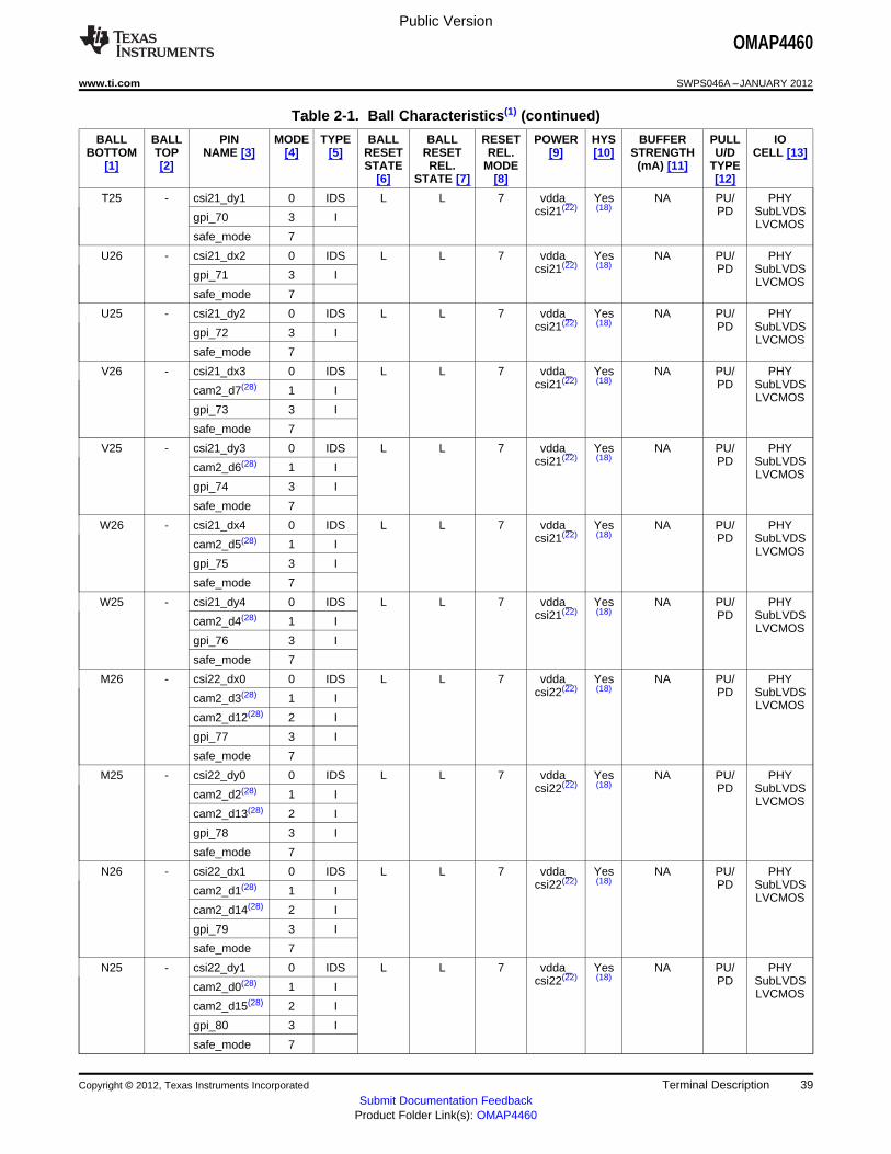
Public Version
OMAP4460
www.ti.com SWPS046A –JANUARY 2012
Table 2-1. Ball Characteristics(1) (continued)
BALL BALL PIN MODE TYPE BALL BALL RESET POWER HYS BUFFER PULL IOBOTTOM TOP NAME [3] [4] [5] RESET RESET REL. [9] [10] STRENGTH U/D CELL [13]
[1] [2] STATE REL. MODE (mA) [11] TYPE[6] STATE [7] [8] [12]
T25 - csi21_dy1 0 IDS L L 7 vdda_ Yes NA PU/ PHYcsi21(22) (18) PD SubLVDSgpi_70 3 I
LVCMOSsafe_mode 7
U26 - csi21_dx2 0 IDS L L 7 vdda_ Yes NA PU/ PHYcsi21(22) (18) PD SubLVDSgpi_71 3 I
LVCMOSsafe_mode 7
U25 - csi21_dy2 0 IDS L L 7 vdda_ Yes NA PU/ PHYcsi21(22) (18) PD SubLVDSgpi_72 3 I
LVCMOSsafe_mode 7
V26 - csi21_dx3 0 IDS L L 7 vdda_ Yes NA PU/ PHYcsi21(22) (18) PD SubLVDScam2_d7(28) 1 I
LVCMOSgpi_73 3 I
safe_mode 7
V25 - csi21_dy3 0 IDS L L 7 vdda_ Yes NA PU/ PHYcsi21(22) (18) PD SubLVDScam2_d6(28) 1 I
LVCMOSgpi_74 3 I
safe_mode 7
W26 - csi21_dx4 0 IDS L L 7 vdda_ Yes NA PU/ PHYcsi21(22) (18) PD SubLVDScam2_d5(28) 1 I
LVCMOSgpi_75 3 I
safe_mode 7
W25 - csi21_dy4 0 IDS L L 7 vdda_ Yes NA PU/ PHYcsi21(22) (18) PD SubLVDScam2_d4(28) 1 I
LVCMOSgpi_76 3 I
safe_mode 7
M26 - csi22_dx0 0 IDS L L 7 vdda_ Yes NA PU/ PHYcsi22(22) (18) PD SubLVDScam2_d3(28) 1 I
LVCMOScam2_d12(28) 2 I
gpi_77 3 I
safe_mode 7
M25 - csi22_dy0 0 IDS L L 7 vdda_ Yes NA PU/ PHYcsi22(22) (18) PD SubLVDScam2_d2(28) 1 I
LVCMOScam2_d13(28) 2 I
gpi_78 3 I
safe_mode 7
N26 - csi22_dx1 0 IDS L L 7 vdda_ Yes NA PU/ PHYcsi22(22) (18) PD SubLVDScam2_d1(28) 1 I
LVCMOScam2_d14(28) 2 I
gpi_79 3 I
safe_mode 7
N25 - csi22_dy1 0 IDS L L 7 vdda_ Yes NA PU/ PHYcsi22(22) (18) PD SubLVDScam2_d0(28) 1 I
LVCMOScam2_d15(28) 2 I
gpi_80 3 I
safe_mode 7
Copyright © 2012, Texas Instruments Incorporated Terminal Description 39Submit Documentation Feedback
Product Folder Link(s): OMAP4460
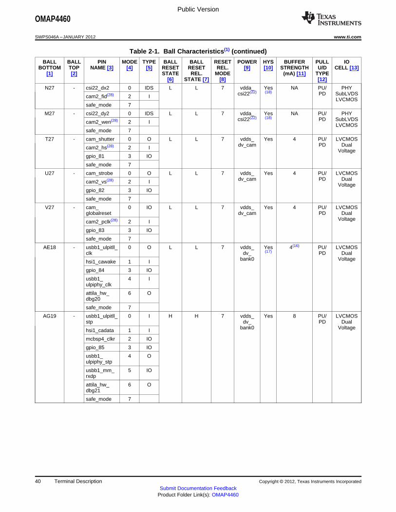
Public Version
OMAP4460
SWPS046A –JANUARY 2012 www.ti.com
Table 2-1. Ball Characteristics(1) (continued)
BALL BALL PIN MODE TYPE BALL BALL RESET POWER HYS BUFFER PULL IOBOTTOM TOP NAME [3] [4] [5] RESET RESET REL. [9] [10] STRENGTH U/D CELL [13]
[1] [2] STATE REL. MODE (mA) [11] TYPE[6] STATE [7] [8] [12]
N27 - csi22_dx2 0 IDS L L 7 vdda_ Yes NA PU/ PHYcsi22(22) (18) PD SubLVDScam2_fid(28) 2 I
LVCMOSsafe_mode 7
M27 - csi22_dy2 0 IDS L L 7 vdda_ Yes NA PU/ PHYcsi22(22) (18) PD SubLVDScam2_wen(28) 2 I
LVCMOSsafe_mode 7
T27 - cam_shutter 0 O L L 7 vdds_ Yes 4 PU/ LVCMOSdv_cam PD Dualcam2_hs(28) 2 I
Voltagegpio_81 3 IO
safe_mode 7
U27 - cam_strobe 0 O L L 7 vdds_ Yes 4 PU/ LVCMOSdv_cam PD Dualcam2_vs(28) 2 I
Voltagegpio_82 3 IO
safe_mode 7
V27 - cam_ 0 IO L L 7 vdds_ Yes 4 PU/ LVCMOSglobalreset dv_cam PD Dual
Voltagecam2_pclk(28) 2 I
gpio_83 3 IO
safe_mode 7
AE18 - usbb1_ulpitll_ 0 O L L 7 vdds_ Yes 4(16) PU/ LVCMOSclk dv_ (17) PD Dual
bank0 Voltagehsi1_cawake 1 I
gpio_84 3 IO
usbb1_ 4 Iulpiphy_clk
attila_hw_ 6 Odbg20
safe_mode 7
AG19 - usbb1_ulpitll_ 0 I H H 7 vdds_ Yes 8 PU/ LVCMOSstp dv_ PD Dual
bank0 Voltagehsi1_cadata 1 I
mcbsp4_clkr 2 IO
gpio_85 3 IO
usbb1_ 4 Oulpiphy_stp
usbb1_mm_ 5 IOrxdp
attila_hw_ 6 Odbg21
safe_mode 7
40 Terminal Description Copyright © 2012, Texas Instruments Incorporated
Submit Documentation FeedbackProduct Folder Link(s): OMAP4460

Public Version
OMAP4460
www.ti.com SWPS046A –JANUARY 2012
Table 2-1. Ball Characteristics(1) (continued)
BALL BALL PIN MODE TYPE BALL BALL RESET POWER HYS BUFFER PULL IOBOTTOM TOP NAME [3] [4] [5] RESET RESET REL. [9] [10] STRENGTH U/D CELL [13]
[1] [2] STATE REL. MODE (mA) [11] TYPE[6] STATE [7] [8] [12]
AF19 - usbb1_ulpitll_ 0 O L L 7 vdds_ Yes 8 PU/ LVCMOSdir dv_ PD Dual
bank0 Voltagehsi1_caflag 1 I
mcbsp4_fsr 2 IO
gpio_86 3 IO
usbb1_ 4 Iulpiphy_dir
attila_hw_ 6 Odbg22
safe_mode 7
AE19 - usbb1_ulpitll_ 0 O L L 7 vdds_ Yes 8 PU/ LVCMOSnxt dv_ PD Dual
bank0 Voltagehsi1_acready 1 O
mcbsp4_fsx 2 IO
gpio_87 3 IO
usbb1_ 4 Iulpiphy_nxt
usbb1_mm_ 5 IOrxdm
attila_hw_ 6 Odbg23
safe_mode 7
AF18 - usbb1_ulpitll_ 0 IO L L 7 vdds_ Yes 8 PU/ LVCMOSdat0 dv_ PD Dual
bank0 Voltagehsi1_acwake 1 O
mcbsp4_clkx 2 IO
gpio_88 3 IO
usbb1_ 4 IOulpiphy_dat0
usbb1_mm_ 5 IOtxen
attila_hw_ 6 Odbg24
safe_mode 7
AG18 - usbb1_ulpitll_ 0 IO L L 7 vdds_ Yes 8 PU/ LVCMOSdat1 dv_ PD Dual
bank0 Voltagehsi1_acdata 1 O
mcbsp4_dx 2 IO
gpio_89 3 IO
usbb1_ 4 IOulpiphy_dat1
usbb1_mm_ 5 IOtxdat
attila_hw_ 6 Odbg25
safe_mode 7
Copyright © 2012, Texas Instruments Incorporated Terminal Description 41Submit Documentation Feedback
Product Folder Link(s): OMAP4460

Public Version
OMAP4460
SWPS046A –JANUARY 2012 www.ti.com
Table 2-1. Ball Characteristics(1) (continued)
BALL BALL PIN MODE TYPE BALL BALL RESET POWER HYS BUFFER PULL IOBOTTOM TOP NAME [3] [4] [5] RESET RESET REL. [9] [10] STRENGTH U/D CELL [13]
[1] [2] STATE REL. MODE (mA) [11] TYPE[6] STATE [7] [8] [12]
AE17 - usbb1_ulpitll_ 0 IO L L 7 vdds_ Yes 8 PU/ LVCMOSdat2 dv_ PD Dual
bank0 Voltagehsi1_acflag 1 O
mcbsp4_dr 2 I
gpio_90 3 IO
usbb1_ 4 IOulpiphy_dat2
usbb1_mm_ 5 IOtxse0
attila_hw_ 6 Odbg26
safe_mode 7
AF17 - usbb1_ulpitll_ 0 IO L L 7 vdds_ Yes 8 PU/ LVCMOSdat3 dv_ PD Dual
bank0 Voltagehsi1_caready 1 I
gpio_91 3 IO
usbb1_ 4 IOulpiphy_dat3
usbb1_mm_ 5 IOrxrcv
attila_hw_ 6 Odbg27
safe_mode 7
AH17 - usbb1_ulpitll_ 0 IO L L 7 vdds_ Yes 8 PU/ LVCMOSdat4 dv_ PD Dual
bank0 Voltagedmtimer8_ 1 IOpwm_evt
abe_mcbsp3 2 I_dr
gpio_92 3 IO
usbb1_ 4 IOulpiphy_dat4
attila_hw_ 6 Odbg28
safe_mode 7
AE16 - usbb1_ulpitll_ 0 IO L L 7 vdds_ Yes 8 PU/ LVCMOSdat5 dv_ PD Dual
bank0 Voltagedmtimer9_ 1 IOpwm_evt
abe_mcbsp3 2 IO_dx
gpio_93 3 IO
usbb1_ 4 IOulpiphy_dat5
attila_hw_ 6 Odbg29
safe_mode 7
42 Terminal Description Copyright © 2012, Texas Instruments Incorporated
Submit Documentation FeedbackProduct Folder Link(s): OMAP4460

Public Version
OMAP4460
www.ti.com SWPS046A –JANUARY 2012
Table 2-1. Ball Characteristics(1) (continued)
BALL BALL PIN MODE TYPE BALL BALL RESET POWER HYS BUFFER PULL IOBOTTOM TOP NAME [3] [4] [5] RESET RESET REL. [9] [10] STRENGTH U/D CELL [13]
[1] [2] STATE REL. MODE (mA) [11] TYPE[6] STATE [7] [8] [12]
AF16 - usbb1_ulpitll_ 0 IO L L 7 vdds_ Yes 8 PU/ LVCMOSdat6 dv_ PD Dual
bank0 Voltagedmtimer10_ 1 IOpwm_evt
abe_mcbsp3 2 IO_clkx
gpio_94 3 IO
usbb1_ 4 IOulpiphy_dat6
abe_dmic_ 5 Idin3
attila_hw_ 6 Odbg30
safe_mode 7
AG16 - usbb1_ulpitll_ 0 IO L L 7 vdds_ Yes 8 PU/ LVCMOSdat7 dv_ PD Dual
bank0 Voltagedmtimer11_ 1 IOpwm_evt
abe_mcbsp3 2 IO_fsx
gpio_95 3 IO
usbb1_ 4 IOulpiphy_dat7
abe_dmic_ 5 Oclk3
attila_hw_ 6 Odbg31
safe_mode 7
AF14 - usbb1_hsic_ 0 IO L L 7 vdds_ NA 0.1 PUy/ LVCMOSdata 1p2v PDy(2)
gpio_96 3 IO
safe_mode 7
AE14 - usbb1_hsic_ 0 IO L L 7 vdds_ NA 0.1 PUy/ LVCMOSstrobe 1p2v PDy(2)
gpio_97 3 IO
safe_mode 7
H4 - sim_io 0 IO L L 7 vdds_ Yes 1 PUy/ LVCMOSusim(27) (15) PDy Dualgpio_wk0 3 IO (9) Voltage
attila_hw_ 6 Odbg1
safe_mode 7
J2 - sim_clk 0 O L L 7 vdds_ Yes 1 PUy/ LVCMOSusim(27) (15) PDy Dualgpio_wk1 3 IO (9) Voltage
attila_hw_ 6 Odbg2
safe_mode 7
G2 - sim_reset 0 O L L 7 vdds_ Yes 1 PUy/ LVCMOSusim(27) (15) PDy Dualgpio_wk2 3 IO (9) Voltage
attila_hw_ 6 Odbg3
safe_mode 7
Copyright © 2012, Texas Instruments Incorporated Terminal Description 43Submit Documentation Feedback
Product Folder Link(s): OMAP4460

Public Version
OMAP4460
SWPS046A –JANUARY 2012 www.ti.com
Table 2-1. Ball Characteristics(1) (continued)
BALL BALL PIN MODE TYPE BALL BALL RESET POWER HYS BUFFER PULL IOBOTTOM TOP NAME [3] [4] [5] RESET RESET REL. [9] [10] STRENGTH U/D CELL [13]
[1] [2] STATE REL. MODE (mA) [11] TYPE[6] STATE [7] [8] [12]
J1 - sim_cd 0 I H H 7 vdds_ Yes 4 PU/ LVCMOS1p8v PDgpio_wk3 3 IO
attila_hw_ 6 Odbg4
safe_mode 7
K1 - sim_pwrctrl 0 O L L 7 vdds_ Yes 4 PU/ LVCMOS1p8v PDgpio_wk4 3 IO
attila_hw_ 6 Odbg5
safe_mode 7
H2 - usbc1_icusb_ 0 IODS L L 7 vdds_ Yes 1 PUy/ LVCMOSdp usim(27) (15) PDy Dual
(10) Voltagegpio_98 3 IOSubLVDS
safe_mode 7
H3 - usbc1_icusb_ 0 IODS L L 7 vdds_ Yes 1 PUy/ LVCMOSdm usim(27) (15) PDy Dual
(10) Voltagegpio_99 3 IOSubLVDS
safe_mode 7
D2 - sdmmc1_clk 0 O L L 7 vdds_ Yes 1 PUy/ LVCMOSsdmmc1 (15) PDy Dualdpm_emu19 2 O (26) (10) Voltage
gpio_100 3 IO
safe_mode 7
E3 - sdmmc1_ 0 IO L L 7 vdds_ Yes 1 PUy/ LVCMOScmd sdmmc1 (15) PDy Dual
(26) (10) Voltageuart1_rx 2 I
gpio_101 3 IO
safe_mode 7
E4 - sdmmc1_ 0 IO L L 7 vdds_ Yes 1 PUy/ LVCMOSdat0 sdmmc1 (15) PDy Dual
(26) (10) Voltagedpm_emu18 2 O
gpio_102 3 IO
safe_mode 7
E2 - sdmmc1_ 0 IO L L 7 vdds_ Yes 1 PUy/ LVCMOSdat1 sdmmc1 (15) PDy Dual
(26) (10) Voltagedpm_emu17 2 O
gpio_103 3 IO
safe_mode 7
E1 - sdmmc1_ 0 IO L L 7 vdds_ Yes 1 PUy/ LVCMOSdat2 sdmmc1 (15) PDy Dual
(26) (10) Voltagedpm_emu16 2 O
gpio_104 3 IO
jtag_tms_ 4 IOtmsc
safe_mode 7
44 Terminal Description Copyright © 2012, Texas Instruments Incorporated
Submit Documentation FeedbackProduct Folder Link(s): OMAP4460
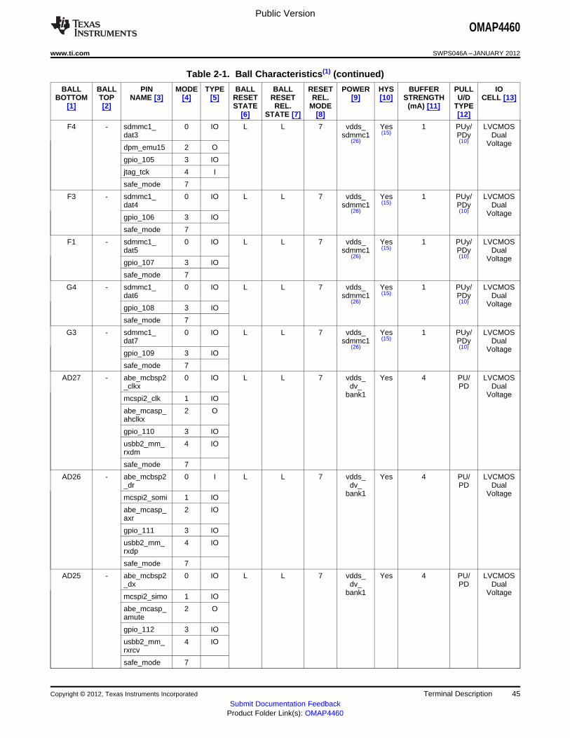
Public Version
OMAP4460
www.ti.com SWPS046A –JANUARY 2012
Table 2-1. Ball Characteristics(1) (continued)
BALL BALL PIN MODE TYPE BALL BALL RESET POWER HYS BUFFER PULL IOBOTTOM TOP NAME [3] [4] [5] RESET RESET REL. [9] [10] STRENGTH U/D CELL [13]
[1] [2] STATE REL. MODE (mA) [11] TYPE[6] STATE [7] [8] [12]
F4 - sdmmc1_ 0 IO L L 7 vdds_ Yes 1 PUy/ LVCMOSdat3 sdmmc1 (15) PDy Dual
(26) (10) Voltagedpm_emu15 2 O
gpio_105 3 IO
jtag_tck 4 I
safe_mode 7
F3 - sdmmc1_ 0 IO L L 7 vdds_ Yes 1 PUy/ LVCMOSdat4 sdmmc1 (15) PDy Dual
(26) (10) Voltagegpio_106 3 IO
safe_mode 7
F1 - sdmmc1_ 0 IO L L 7 vdds_ Yes 1 PUy/ LVCMOSdat5 sdmmc1 (15) PDy Dual
(26) (10) Voltagegpio_107 3 IO
safe_mode 7
G4 - sdmmc1_ 0 IO L L 7 vdds_ Yes 1 PUy/ LVCMOSdat6 sdmmc1 (15) PDy Dual
(26) (10) Voltagegpio_108 3 IO
safe_mode 7
G3 - sdmmc1_ 0 IO L L 7 vdds_ Yes 1 PUy/ LVCMOSdat7 sdmmc1 (15) PDy Dual
(26) (10) Voltagegpio_109 3 IO
safe_mode 7
AD27 - abe_mcbsp2 0 IO L L 7 vdds_ Yes 4 PU/ LVCMOS_clkx dv_ PD Dual
bank1 Voltagemcspi2_clk 1 IO
abe_mcasp_ 2 Oahclkx
gpio_110 3 IO
usbb2_mm_ 4 IOrxdm
safe_mode 7
AD26 - abe_mcbsp2 0 I L L 7 vdds_ Yes 4 PU/ LVCMOS_dr dv_ PD Dual
bank1 Voltagemcspi2_somi 1 IO
abe_mcasp_ 2 IOaxr
gpio_111 3 IO
usbb2_mm_ 4 IOrxdp
safe_mode 7
AD25 - abe_mcbsp2 0 IO L L 7 vdds_ Yes 4 PU/ LVCMOS_dx dv_ PD Dual
bank1 Voltagemcspi2_simo 1 IO
abe_mcasp_ 2 Oamute
gpio_112 3 IO
usbb2_mm_ 4 IOrxrcv
safe_mode 7
Copyright © 2012, Texas Instruments Incorporated Terminal Description 45Submit Documentation Feedback
Product Folder Link(s): OMAP4460

Public Version
OMAP4460
SWPS046A –JANUARY 2012 www.ti.com
Table 2-1. Ball Characteristics(1) (continued)
BALL BALL PIN MODE TYPE BALL BALL RESET POWER HYS BUFFER PULL IOBOTTOM TOP NAME [3] [4] [5] RESET RESET REL. [9] [10] STRENGTH U/D CELL [13]
[1] [2] STATE REL. MODE (mA) [11] TYPE[6] STATE [7] [8] [12]
AC28 - abe_mcbsp2 0 IO L L 7 vdds_ Yes 4 PU/ LVCMOS_fsx dv_ PD Dual
bank1 Voltagemcspi2_cs0 1 IO
abe_mcasp_ 2 Oafsx
gpio_113 3 IO
usbb2_mm_ 4 IOtxen
safe_mode 7
AC26 - abe_mcbsp1 0 IO L L 7 vdds_ Yes 4 PU/ LVCMOS_clkx dv_ PD Dual
bank1 Voltageabe_slimbus1 1 IO_clock
gpio_114 3 IO
safe_mode 7
AC25 - abe_mcbsp1 0 I L L 7 vdds_ Yes 4 PU/ LVCMOS_dr dv_ PD Dual
bank1 Voltageabe_slimbus1 1 IO_data
gpio_115 3 IO
safe_mode 7
AB25 - abe_mcbsp1 0 IO L L 7 vdds_ Yes 4 PU/ LVCMOS_dx dv_ PD Dual
bank1 Voltagesdmmc3_ 1 IOdat2
abe_mcasp_ 2 Oaclkx
gpio_116 3 IO
safe_mode 7
AC27 - abe_mcbsp1 0 IO L L 7 vdds_ Yes 4 PU/ LVCMOS_fsx dv_ PD Dual
bank1 Voltagesdmmc3_ 1 IOdat3
abe_mcasp_ 2 Iamutein
gpio_117 3 IO
safe_mode 7
AG25 - abe_pdm_ul_ 0 I L L 7 vdds_ Yes 4 PU/ LVCMOSdata dv_ PD Dual
bank2 Voltageabe_mcbsp3 1 I_dr
safe_mode 7
AF25 - abe_pdm_dl_ 0 O L L 7 vdds_ Yes 4 PU/ LVCMOSdata dv_ PD Dual
bank2 Voltageabe_mcbsp3 1 IO_dx
safe_mode 7
46 Terminal Description Copyright © 2012, Texas Instruments Incorporated
Submit Documentation FeedbackProduct Folder Link(s): OMAP4460

Public Version
OMAP4460
www.ti.com SWPS046A –JANUARY 2012
Table 2-1. Ball Characteristics(1) (continued)
BALL BALL PIN MODE TYPE BALL BALL RESET POWER HYS BUFFER PULL IOBOTTOM TOP NAME [3] [4] [5] RESET RESET REL. [9] [10] STRENGTH U/D CELL [13]
[1] [2] STATE REL. MODE (mA) [11] TYPE[6] STATE [7] [8] [12]
AE25 - abe_pdm_ 0 IO L L 7 vdds_ Yes 4 PU/ LVCMOSframe dv_ PD Dual
bank2 Voltageabe_mcbsp3 1 IO_clkx
safe_mode 7
AF26 - abe_pdm_lb_ 0 O L L 7 vdds_ Yes 4 PU/ LVCMOSclk dv_ PD Dual
bank2 Voltageabe_mcbsp3 1 IO_fsx
safe_mode 7
AH26 - abe_clks 0 I L L 7 vdds_ Yes 4 PU/ LVCMOSdv_ PD Dualgpio_118 3 IO
bank2 Voltagesafe_mode 7
AE24 - abe_dmic_ 0 O L L 7 vdds_ Yes 4 PU/ LVCMOSclk1 dv_ PD Dual
bank2 Voltagegpio_119 3 IO
usbb2_mm_ 4 IOtxse0
uart4_cts 5 I
safe_mode 7
AF24 - abe_dmic_ 0 I L L 7 vdds_ Yes 4 PU/ LVCMOSdin1 dv_ PD Dual
bank2 Voltagegpio_120 3 IO
usbb2_mm_ 4 IOtxdat
uart4_rts 5 O
safe_mode 7
AG24 - abe_dmic_ 0 I L L 7 vdds_ Yes 4 PU/ LVCMOSdin2 dv_ PD Dual
bank2 Voltageslimbus2_ 1 IOclock
abe_mcasp 2_axr
gpio_121 3 IO
dmtimer11_ 5 IOpwm_evt
safe_mode 7
AH24 - abe_dmic_ 0 I L L 7 vdds_ Yes 4 PU/ LVCMOSdin3 dv_ PD Dual
bank2 Voltageslimbus2_ 1 IOdata
abe_dmic_ 2 Oclk2
gpio_122 3 IO
dmtimer9_ 5 IOpwm_evt
safe_mode 7
Copyright © 2012, Texas Instruments Incorporated Terminal Description 47Submit Documentation Feedback
Product Folder Link(s): OMAP4460

Public Version
OMAP4460
SWPS046A –JANUARY 2012 www.ti.com
Table 2-1. Ball Characteristics(1) (continued)
BALL BALL PIN MODE TYPE BALL BALL RESET POWER HYS BUFFER PULL IOBOTTOM TOP NAME [3] [4] [5] RESET RESET REL. [9] [10] STRENGTH U/D CELL [13]
[1] [2] STATE REL. MODE (mA) [11] TYPE[6] STATE [7] [8] [12]
AB26 - uart2_cts 0 I H H 7 vdds_ Yes 4 PU/ LVCMOSdv_ PD Dualsdmmc3_clk 1 O
bank1 Voltagegpio_123 3 IO
safe_mode 7
AB27 - uart2_rts 0 O H H 7 vdds_ Yes 4 PU/ LVCMOSdv_ PD Dualsdmmc3_ 1 IO
bank1 Voltagecmd
gpio_124 3 IO
safe_mode 7
AA25 - uart2_rx 0 I H H 7 vdds_ Yes 4 PU/ LVCMOSdv_ PD Dualsdmmc3_ 1 IO
bank1 Voltagedat0
gpio_125 3 IO
safe_mode 7
AA26 - uart2_tx 0 O H H 7 vdds_ Yes 4 PU/ LVCMOSdv_ PD Dualsdmmc3_ 1 IO
bank1 Voltagedat1
gpio_126 3 IO
safe_mode 7
AA27 - hdq_sio 0 IOD Z Z 7 vdds_ Yes 4 PU/ LVCMOS1p8v PD Openi2c3_sccb 1 OD
Draini2c2_sccb 2 OD
gpio_127 3 IO
safe_mode 7
AE28 - i2c1_scl 0 OD H H 0 vdds_ Yes 3 PUx/ LVCMOSdv_ PDy- Open
bank2 OD (5) Drain DualVoltage
AE26 - i2c1_sda 0 IOD H H 0 vdds_ Yes 3 PUx/ LVCMOSdv_ PDy- Open
bank2 OD (5) Drain DualVoltage
C26 - i2c2_scl 0 OD H H 7 vdds_ Yes 3 PUx/ LVCMOS1p8v PDy- Openuart1_rx 1 I 4
GPIO Draingpio_128 3 IO 4 (5)
safe_mode 7 4
D26 - i2c2_sda 0 IOD H H 7 vdds_ Yes 3 PUx/ LVCMOS1p8v PDy- Openuart1_tx 1 O 4
GPIO Draingpio_129 3 IO 4 (5)
safe_mode 7 4
W27 - i2c3_scl 0 OD H H 7 vdds_ Yes 3 PUx/ LVCMOSdv_cam PDy- Opengpio_130 3 IO 4
GPIO Drain Dualsafe_mode 7 4 (5) Voltage
Y27 - i2c3_sda 0 IOD H H 7 vdds_ Yes 3 PUx/ LVCMOSdv_cam PDy- Opengpio_131 3 IO 4
GPIO Drain Dualsafe_mode 7 4 (5) Voltage
48 Terminal Description Copyright © 2012, Texas Instruments Incorporated
Submit Documentation FeedbackProduct Folder Link(s): OMAP4460

Public Version
OMAP4460
www.ti.com SWPS046A –JANUARY 2012
Table 2-1. Ball Characteristics(1) (continued)
BALL BALL PIN MODE TYPE BALL BALL RESET POWER HYS BUFFER PULL IOBOTTOM TOP NAME [3] [4] [5] RESET RESET REL. [9] [10] STRENGTH U/D CELL [13]
[1] [2] STATE REL. MODE (mA) [11] TYPE[6] STATE [7] [8] [12]
AG21 - i2c4_scl 0 OD H H 7 vdds_ Yes 3 PUx/ LVCMOSdv_ PDy- Opengpio_132 3 IO 4
bank5 GPIO Drain Dualsafe_mode 7 4 (5) Voltage
AH22 - i2c4_sda 0 IOD H H 7 vdds_ Yes 3 PUx/ LVCMOSdv_ PDy- Opengpio_133 3 IO 4
bank5 GPIO Drain Dualsafe_mode 7 4 (5) Voltage
AG9 - sr_scl 0 OD H H 0 vdds_ Yes 3 PUx/ LVCMOSdv_ PDy- Open
bank2 OD (5) Drain DualVoltage
AF9 - sr_sda 0 IOD H H 0 vdds_ Yes 3 PUx/ LVCMOSdv_ PDy- Open
bank2 OD (5) Drain DualVoltage
AF22 - mcspi1_clk 0 IO L L 7 vdds_ Yes 4 PU/ LVCMOSdv_ PD Dualgpio_134 3 IO
bank3 Voltagesafe_mode 7
AE22 - mcspi1_somi 0 IO L L 7 vdds_ Yes 4 PU/ LVCMOSdv_ PD Dualgpio_135 3 IO
bank3 Voltagesafe_mode 7
AG22 - mcspi1_simo 0 IO L L 7 vdds_ Yes 4 PU/ LVCMOSdv_ PD Dualgpio_136 3 IO
bank3 Voltagesafe_mode 7
AE23 - mcspi1_cs0 0 IO L L 7 vdds_ Yes 4 PU/ LVCMOSdv_ PD Dualgpio_137 3 IO
bank3 Voltagesafe_mode 7
AF23 - mcspi1_cs1 0 O L L 7 vdds_ Yes 4 PU/ LVCMOSdv_ PD Dualuart1_rx 1 I
bank3 Voltagegpio_138 3 IO
safe_mode 7
AG23 - mcspi1_cs2 0 O H H 7 vdds_ Yes 4 PU/ LVCMOSdv_ PD Dualuart1_cts 1 I
bank3 Voltageslimbus2_ 2 IOclock
gpio_139 3 IO
safe_mode 7
AH23 - mcspi1_cs3 0 O H H 7 vdds_ Yes 4 PU/ LVCMOSdv_ (16) PD Dualuart1_rts 1 O
bank3 Voltageslimbus2_ 2 IOdata
gpio_140 3 IO
safe_mode 7
F27 - uart3_cts_ 0 IO H H 7 vdds_ Yes 4 PU/ LVCMOSrctx 1p8v PD
uart1_tx 1 O
gpio_141 3 IO
safe_mode 7
Copyright © 2012, Texas Instruments Incorporated Terminal Description 49Submit Documentation Feedback
Product Folder Link(s): OMAP4460
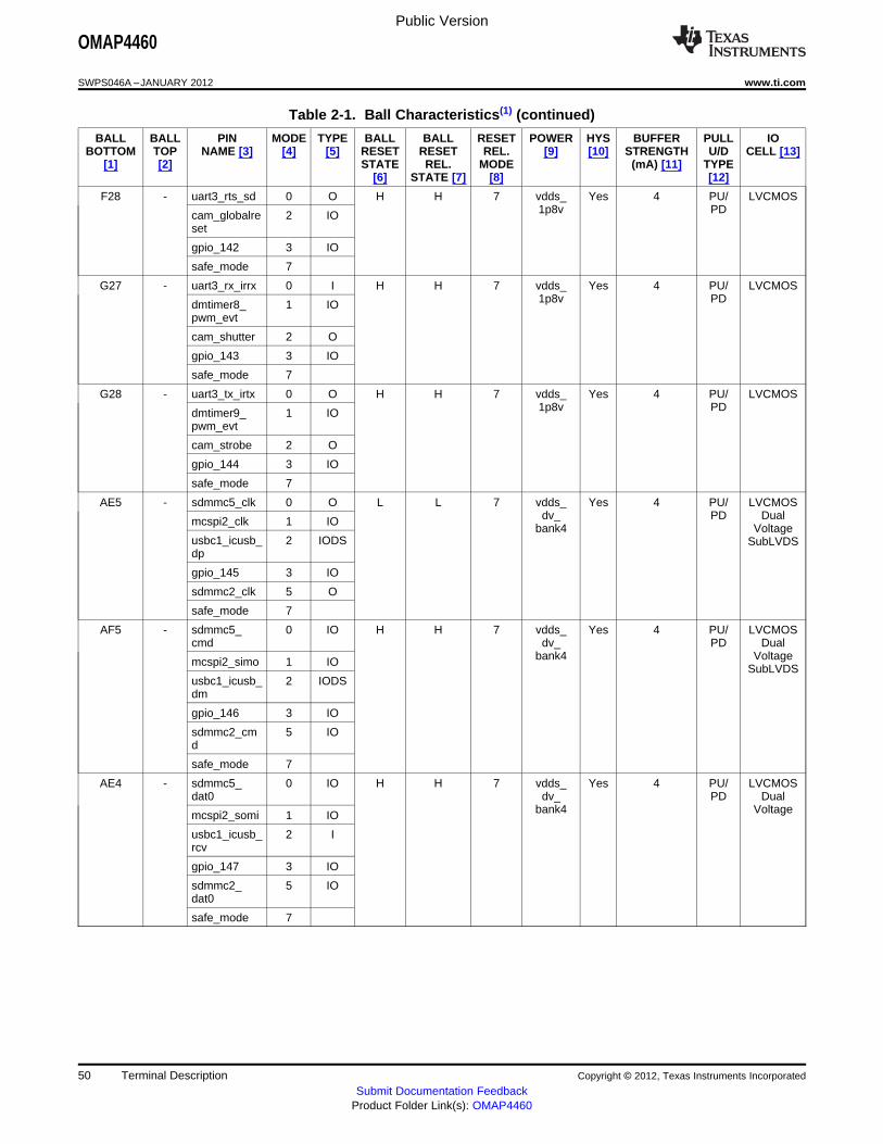
Public Version
OMAP4460
SWPS046A –JANUARY 2012 www.ti.com
Table 2-1. Ball Characteristics(1) (continued)
BALL BALL PIN MODE TYPE BALL BALL RESET POWER HYS BUFFER PULL IOBOTTOM TOP NAME [3] [4] [5] RESET RESET REL. [9] [10] STRENGTH U/D CELL [13]
[1] [2] STATE REL. MODE (mA) [11] TYPE[6] STATE [7] [8] [12]
F28 - uart3_rts_sd 0 O H H 7 vdds_ Yes 4 PU/ LVCMOS1p8v PDcam_globalre 2 IO
set
gpio_142 3 IO
safe_mode 7
G27 - uart3_rx_irrx 0 I H H 7 vdds_ Yes 4 PU/ LVCMOS1p8v PDdmtimer8_ 1 IO
pwm_evt
cam_shutter 2 O
gpio_143 3 IO
safe_mode 7
G28 - uart3_tx_irtx 0 O H H 7 vdds_ Yes 4 PU/ LVCMOS1p8v PDdmtimer9_ 1 IO
pwm_evt
cam_strobe 2 O
gpio_144 3 IO
safe_mode 7
AE5 - sdmmc5_clk 0 O L L 7 vdds_ Yes 4 PU/ LVCMOSdv_ PD Dualmcspi2_clk 1 IO
bank4 Voltageusbc1_icusb_ 2 IODS SubLVDSdp
gpio_145 3 IO
sdmmc2_clk 5 O
safe_mode 7
AF5 - sdmmc5_ 0 IO H H 7 vdds_ Yes 4 PU/ LVCMOScmd dv_ PD Dual
bank4 Voltagemcspi2_simo 1 IOSubLVDS
usbc1_icusb_ 2 IODSdm
gpio_146 3 IO
sdmmc2_cm 5 IOd
safe_mode 7
AE4 - sdmmc5_ 0 IO H H 7 vdds_ Yes 4 PU/ LVCMOSdat0 dv_ PD Dual
bank4 Voltagemcspi2_somi 1 IO
usbc1_icusb_ 2 Ircv
gpio_147 3 IO
sdmmc2_ 5 IOdat0
safe_mode 7
50 Terminal Description Copyright © 2012, Texas Instruments Incorporated
Submit Documentation FeedbackProduct Folder Link(s): OMAP4460
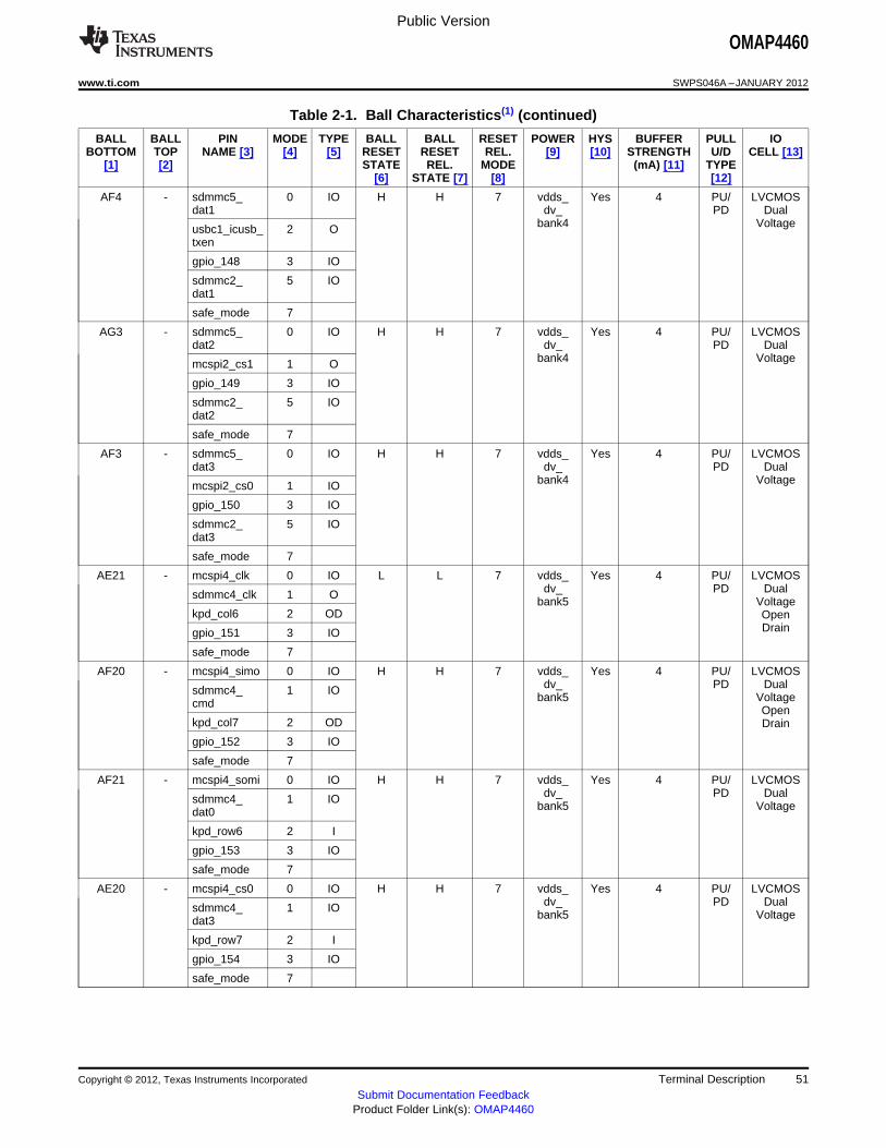
Public Version
OMAP4460
www.ti.com SWPS046A –JANUARY 2012
Table 2-1. Ball Characteristics(1) (continued)
BALL BALL PIN MODE TYPE BALL BALL RESET POWER HYS BUFFER PULL IOBOTTOM TOP NAME [3] [4] [5] RESET RESET REL. [9] [10] STRENGTH U/D CELL [13]
[1] [2] STATE REL. MODE (mA) [11] TYPE[6] STATE [7] [8] [12]
AF4 - sdmmc5_ 0 IO H H 7 vdds_ Yes 4 PU/ LVCMOSdat1 dv_ PD Dual
bank4 Voltageusbc1_icusb_ 2 Otxen
gpio_148 3 IO
sdmmc2_ 5 IOdat1
safe_mode 7
AG3 - sdmmc5_ 0 IO H H 7 vdds_ Yes 4 PU/ LVCMOSdat2 dv_ PD Dual
bank4 Voltagemcspi2_cs1 1 O
gpio_149 3 IO
sdmmc2_ 5 IOdat2
safe_mode 7
AF3 - sdmmc5_ 0 IO H H 7 vdds_ Yes 4 PU/ LVCMOSdat3 dv_ PD Dual
bank4 Voltagemcspi2_cs0 1 IO
gpio_150 3 IO
sdmmc2_ 5 IOdat3
safe_mode 7
AE21 - mcspi4_clk 0 IO L L 7 vdds_ Yes 4 PU/ LVCMOSdv_ PD Dualsdmmc4_clk 1 O
bank5 Voltagekpd_col6 2 OD Open
Draingpio_151 3 IO
safe_mode 7
AF20 - mcspi4_simo 0 IO H H 7 vdds_ Yes 4 PU/ LVCMOSdv_ PD Dualsdmmc4_ 1 IO
bank5 VoltagecmdOpen
kpd_col7 2 OD Drain
gpio_152 3 IO
safe_mode 7
AF21 - mcspi4_somi 0 IO H H 7 vdds_ Yes 4 PU/ LVCMOSdv_ PD Dualsdmmc4_ 1 IO
bank5 Voltagedat0
kpd_row6 2 I
gpio_153 3 IO
safe_mode 7
AE20 - mcspi4_cs0 0 IO H H 7 vdds_ Yes 4 PU/ LVCMOSdv_ PD Dualsdmmc4_ 1 IO
bank5 Voltagedat3
kpd_row7 2 I
gpio_154 3 IO
safe_mode 7
Copyright © 2012, Texas Instruments Incorporated Terminal Description 51Submit Documentation Feedback
Product Folder Link(s): OMAP4460

Public Version
OMAP4460
SWPS046A –JANUARY 2012 www.ti.com
Table 2-1. Ball Characteristics(1) (continued)
BALL BALL PIN MODE TYPE BALL BALL RESET POWER HYS BUFFER PULL IOBOTTOM TOP NAME [3] [4] [5] RESET RESET REL. [9] [10] STRENGTH U/D CELL [13]
[1] [2] STATE REL. MODE (mA) [11] TYPE[6] STATE [7] [8] [12]
AG20 - uart4_rx 0 I H H 7 vdds_ Yes 4 PU/ LVCMOSdv_ PD Dualsdmmc4_ 1 IO
bank5 Voltagedat2
kpd_row8 2 I
gpio_155 3 IO
safe_mode 7
AH19 - uart4_tx 0 O H H 7 vdds_ Yes 4 PU/ LVCMOSdv_ PD Dualsdmmc4_ 1 IO
bank5 Voltagedat1Open
kpd_col8 2 OD Drain
gpio_156 3 IO
safe_mode 7
AG12 - usbb2_ulpitll_ 0 O L L 7 vdds_ Yes 4(16) PU/ LVCMOSclk dv_ (17) PD Dual
bank6 Voltageusbb2_ 1 Iulpiphy_clk
sdmmc4_ 2 IOcmd
gpio_157 3 IO
hsi2_cawake 4 I
safe_mode 7
AF12 - usbb2_ulpitll_ 0 I H H 7 vdds_ Yes 4(16) PU/ LVCMOSstp dv_ PD Dual
bank6 Voltageusbb2_ 1 Oulpiphy_stp
sdmmc4_clk 2 O
gpio_158 3 IO
hsi2_cadata 4 I
dispc2_ 5 Odata23
safe_mode 7
AE12 - usbb2_ulpitll_ 0 O H H 7 vdds_ Yes 4(16) PU/ LVCMOSdir dv_ PD Dual
bank6 Voltageusbb2_ 1 Iulpiphy_dir
sdmmc4_ 2 IOdat0
gpio_159 3 IO
hsi2_caflag 4 I
dispc2_ 5 Odata22
safe_mode 7
52 Terminal Description Copyright © 2012, Texas Instruments Incorporated
Submit Documentation FeedbackProduct Folder Link(s): OMAP4460

Public Version
OMAP4460
www.ti.com SWPS046A –JANUARY 2012
Table 2-1. Ball Characteristics(1) (continued)
BALL BALL PIN MODE TYPE BALL BALL RESET POWER HYS BUFFER PULL IOBOTTOM TOP NAME [3] [4] [5] RESET RESET REL. [9] [10] STRENGTH U/D CELL [13]
[1] [2] STATE REL. MODE (mA) [11] TYPE[6] STATE [7] [8] [12]
AG13 - usbb2_ulpitll_ 0 O H H 7 vdds_ Yes 4(16) PU/ LVCMOSnxt dv_ PD Dual
bank6 Voltageusbb2_ 1 Iulpiphy_nxt
sdmmc4_ 2 IOdat1
gpio_160 3 IO
hsi2_acready 4 O
dispc2_ 5 Odata21
safe_mode 7
AE11 - usbb2_ulpitll_ 0 IO H H 7 vdds_ Yes 4(16) PU/ LVCMOSdat0 dv_ PD Dual
bank6 Voltageusbb2_ 1 IOulpiphy_dat0
sdmmc4_ 2 IOdat2
gpio_161 3 IO
hsi2_acwake 4 O
dispc2_ 5 Odata20
usbb2_ 6 IOmm_txen
safe_mode 7
AF11 - usbb2_ulpitll_ 0 IO H H 7 vdds_ Yes 4(16) PU/ LVCMOSdat1 dv_ PD Dual
bank6 Voltageusbb2_ 1 IOulpiphy_dat1
sdmmc4_ 2 IOdat3
gpio_162 3 IO
hsi2_acdata 4 O
dispc2_ 5 Odata19
usbb2_ 6 IOmm_txdat
safe_mode 7
AG11 - usbb2_ulpitll_ 0 IO L L 7 vdds_ Yes 4(16) PU/ LVCMOSdat2 dv_ PD Dual
bank6 Voltageusbb2_ 1 IOulpiphy_dat2
sdmmc3_ 2 IOdat2
gpio_163 3 IO
hsi2_acflag 4 O
dispc2_ 5 Odata18
usbb2_ 6 IOmm_txse0
safe_mode 7
Copyright © 2012, Texas Instruments Incorporated Terminal Description 53Submit Documentation Feedback
Product Folder Link(s): OMAP4460
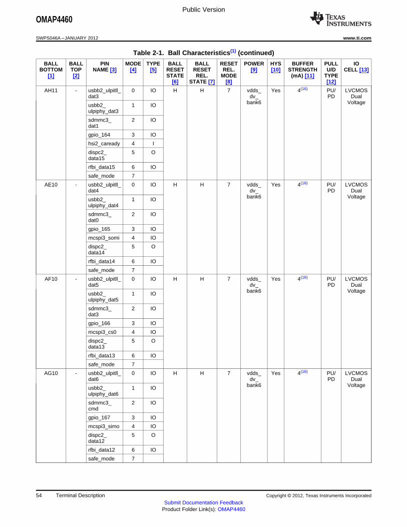
Public Version
OMAP4460
SWPS046A –JANUARY 2012 www.ti.com
Table 2-1. Ball Characteristics(1) (continued)
BALL BALL PIN MODE TYPE BALL BALL RESET POWER HYS BUFFER PULL IOBOTTOM TOP NAME [3] [4] [5] RESET RESET REL. [9] [10] STRENGTH U/D CELL [13]
[1] [2] STATE REL. MODE (mA) [11] TYPE[6] STATE [7] [8] [12]
AH11 - usbb2_ulpitll_ 0 IO H H 7 vdds_ Yes 4(16) PU/ LVCMOSdat3 dv_ PD Dual
bank6 Voltageusbb2_ 1 IOulpiphy_dat3
sdmmc3_ 2 IOdat1
gpio_164 3 IO
hsi2_caready 4 I
dispc2_ 5 Odata15
rfbi_data15 6 IO
safe_mode 7
AE10 - usbb2_ulpitll_ 0 IO H H 7 vdds_ Yes 4(16) PU/ LVCMOSdat4 dv_ PD Dual
bank6 Voltageusbb2_ 1 IOulpiphy_dat4
sdmmc3_ 2 IOdat0
gpio_165 3 IO
mcspi3_somi 4 IO
dispc2_ 5 Odata14
rfbi_data14 6 IO
safe_mode 7
AF10 - usbb2_ulpitll_ 0 IO H H 7 vdds_ Yes 4(16) PU/ LVCMOSdat5 dv_ PD Dual
bank6 Voltageusbb2_ 1 IOulpiphy_dat5
sdmmc3_ 2 IOdat3
gpio_166 3 IO
mcspi3_cs0 4 IO
dispc2_ 5 Odata13
rfbi_data13 6 IO
safe_mode 7
AG10 - usbb2_ulpitll_ 0 IO H H 7 vdds_ Yes 4(16) PU/ LVCMOSdat6 dv_ PD Dual
bank6 Voltageusbb2_ 1 IOulpiphy_dat6
sdmmc3_ 2 IOcmd
gpio_167 3 IO
mcspi3_simo 4 IO
dispc2_ 5 Odata12
rfbi_data12 6 IO
safe_mode 7
54 Terminal Description Copyright © 2012, Texas Instruments Incorporated
Submit Documentation FeedbackProduct Folder Link(s): OMAP4460
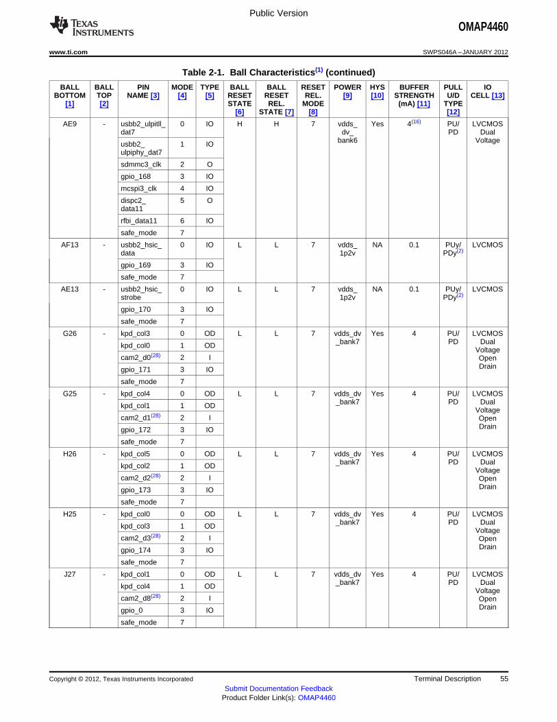
Public Version
OMAP4460
www.ti.com SWPS046A –JANUARY 2012
Table 2-1. Ball Characteristics(1) (continued)
BALL BALL PIN MODE TYPE BALL BALL RESET POWER HYS BUFFER PULL IOBOTTOM TOP NAME [3] [4] [5] RESET RESET REL. [9] [10] STRENGTH U/D CELL [13]
[1] [2] STATE REL. MODE (mA) [11] TYPE[6] STATE [7] [8] [12]
AE9 - usbb2_ulpitll_ 0 IO H H 7 vdds_ Yes 4(16) PU/ LVCMOSdat7 dv_ PD Dual
bank6 Voltageusbb2_ 1 IOulpiphy_dat7
sdmmc3_clk 2 O
gpio_168 3 IO
mcspi3_clk 4 IO
dispc2_ 5 Odata11
rfbi_data11 6 IO
safe_mode 7
AF13 - usbb2_hsic_ 0 IO L L 7 vdds_ NA 0.1 PUy/ LVCMOSdata 1p2v PDy(2)
gpio_169 3 IO
safe_mode 7
AE13 - usbb2_hsic_ 0 IO L L 7 vdds_ NA 0.1 PUy/ LVCMOSstrobe 1p2v PDy(2)
gpio_170 3 IO
safe_mode 7
G26 - kpd_col3 0 OD L L 7 vdds_dv Yes 4 PU/ LVCMOS_bank7 PD Dualkpd_col0 1 OD
Voltagecam2_d0(28) 2 I Open
Draingpio_171 3 IO
safe_mode 7
G25 - kpd_col4 0 OD L L 7 vdds_dv Yes 4 PU/ LVCMOS_bank7 PD Dualkpd_col1 1 OD
Voltagecam2_d1(28) 2 I Open
Draingpio_172 3 IO
safe_mode 7
H26 - kpd_col5 0 OD L L 7 vdds_dv Yes 4 PU/ LVCMOS_bank7 PD Dualkpd_col2 1 OD
Voltagecam2_d2(28) 2 I Open
Draingpio_173 3 IO
safe_mode 7
H25 - kpd_col0 0 OD L L 7 vdds_dv Yes 4 PU/ LVCMOS_bank7 PD Dualkpd_col3 1 OD
Voltagecam2_d3(28) 2 I Open
Draingpio_174 3 IO
safe_mode 7
J27 - kpd_col1 0 OD L L 7 vdds_dv Yes 4 PU/ LVCMOS_bank7 PD Dualkpd_col4 1 OD
Voltagecam2_d8(28) 2 I Open
Draingpio_0 3 IO
safe_mode 7
Copyright © 2012, Texas Instruments Incorporated Terminal Description 55Submit Documentation Feedback
Product Folder Link(s): OMAP4460
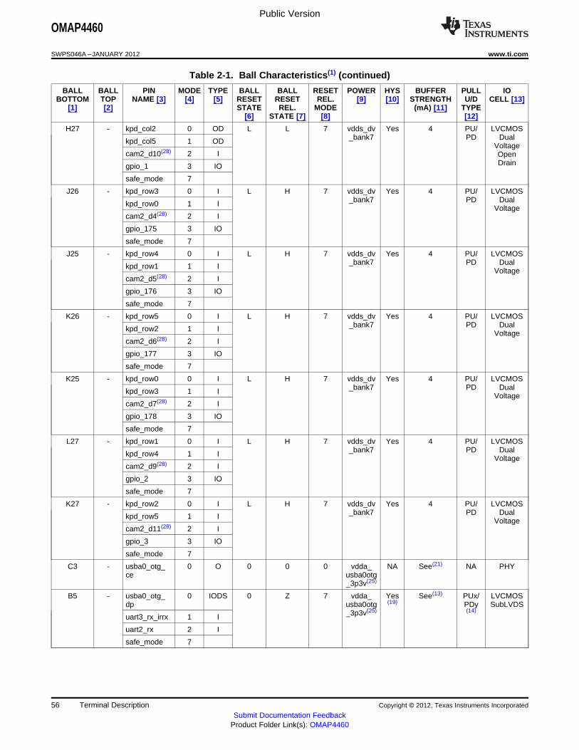
Public Version
OMAP4460
SWPS046A –JANUARY 2012 www.ti.com
Table 2-1. Ball Characteristics(1) (continued)
BALL BALL PIN MODE TYPE BALL BALL RESET POWER HYS BUFFER PULL IOBOTTOM TOP NAME [3] [4] [5] RESET RESET REL. [9] [10] STRENGTH U/D CELL [13]
[1] [2] STATE REL. MODE (mA) [11] TYPE[6] STATE [7] [8] [12]
H27 - kpd_col2 0 OD L L 7 vdds_dv Yes 4 PU/ LVCMOS_bank7 PD Dualkpd_col5 1 OD
Voltagecam2_d10(28) 2 I Open
Draingpio_1 3 IO
safe_mode 7
J26 - kpd_row3 0 I L H 7 vdds_dv Yes 4 PU/ LVCMOS_bank7 PD Dualkpd_row0 1 I
Voltagecam2_d4(28) 2 I
gpio_175 3 IO
safe_mode 7
J25 - kpd_row4 0 I L H 7 vdds_dv Yes 4 PU/ LVCMOS_bank7 PD Dualkpd_row1 1 I
Voltagecam2_d5(28) 2 I
gpio_176 3 IO
safe_mode 7
K26 - kpd_row5 0 I L H 7 vdds_dv Yes 4 PU/ LVCMOS_bank7 PD Dualkpd_row2 1 I
Voltagecam2_d6(28) 2 I
gpio_177 3 IO
safe_mode 7
K25 - kpd_row0 0 I L H 7 vdds_dv Yes 4 PU/ LVCMOS_bank7 PD Dualkpd_row3 1 I
Voltagecam2_d7(28) 2 I
gpio_178 3 IO
safe_mode 7
L27 - kpd_row1 0 I L H 7 vdds_dv Yes 4 PU/ LVCMOS_bank7 PD Dualkpd_row4 1 I
Voltagecam2_d9(28) 2 I
gpio_2 3 IO
safe_mode 7
K27 - kpd_row2 0 I L H 7 vdds_dv Yes 4 PU/ LVCMOS_bank7 PD Dualkpd_row5 1 I
Voltagecam2_d11(28) 2 I
gpio_3 3 IO
safe_mode 7
C3 - usba0_otg_ 0 O 0 0 0 vdda_ NA See(21) NA PHYce usba0otg
_3p3v(25)
B5 - usba0_otg_ 0 IODS 0 Z 7 vdda_ Yes See(13) PUx/ LVCMOSdp usba0otg (19) PDy SubLVDS
_3p3v(25) (14)uart3_rx_irrx 1 I
uart2_rx 2 I
safe_mode 7
56 Terminal Description Copyright © 2012, Texas Instruments Incorporated
Submit Documentation FeedbackProduct Folder Link(s): OMAP4460

Public Version
OMAP4460
www.ti.com SWPS046A –JANUARY 2012
Table 2-1. Ball Characteristics(1) (continued)
BALL BALL PIN MODE TYPE BALL BALL RESET POWER HYS BUFFER PULL IOBOTTOM TOP NAME [3] [4] [5] RESET RESET REL. [9] [10] STRENGTH U/D CELL [13]
[1] [2] STATE REL. MODE (mA) [11] TYPE[6] STATE [7] [8] [12]
B4 - usba0_otg_ 0 IODS 0 Z 7 vdda_ Yes See(13) PUx/ LVCMOSdm usba0otg (19) PDy SubLVDS
_3p3v(25) (14)uart3_tx_irtx 1 O
uart2_tx 2 O
safe_mode 7
AH6 - fref_xtal_in 0 AI-I Z Z 0 vdds_ Yes NA NA LVCMOS1p8_fref Analog
AH5 - fref_xtal_out 0 AO Z NA 0 vdds_ NA NA NA OSC1p8_fref
AG5 - fref_xtal_ 0 NA NA NA NA NA NA NA NA NAvssosc
AG8 - fref_slicer_in 0 AI-I Z Z 0 vdds_ NA NA NA LVCMOS1p8_fref Analoggpi_wk5 3 I
safe_mode 7
AD1 - fref_clk_ioreq 0 O L L 0 vdds_ Yes 4 PU/ LVCMOS1p8_fref PD
AD2 - fref_clk0_out 0 O L L 7 vdds_ Yes 4 PU/ LVCMOS1p8_fref PDfref_clk1_req 1 I
sys_drm_ 2 Omsecure
gpio_wk6 3 IO
sdmmc2_ 5 IOdat7
attila_hw_dbg 6 O6
safe_mode 7
AA28 - fref_clk1_out 0 O L L 7 vdds_ Yes 4 PU/ LVCMOSdv_cam PD Dualgpio_181 3 IO
Voltagesafe_mode 7
Y28 - fref_clk2_out 0 O L L 7 vdds_ Yes 4 PU/ LVCMOSdv_cam PD Dualgpio_182 3 IO
Voltagesafe_mode 7
AD3 - fref_clk3_req 0 I L L 7 vdds_ Yes 4 PU/ LVCMOSdv_ fref PD Dualfref_clk1_req 1 I
Voltagesys_drm_ 2 Omsecure
gpio_wk30 3 IO
sdmmc2_ 5 IOdat4
attila_hw_ 6 Odbg7
safe_mode 7
Copyright © 2012, Texas Instruments Incorporated Terminal Description 57Submit Documentation Feedback
Product Folder Link(s): OMAP4460

Public Version
OMAP4460
SWPS046A –JANUARY 2012 www.ti.com
Table 2-1. Ball Characteristics(1) (continued)
BALL BALL PIN MODE TYPE BALL BALL RESET POWER HYS BUFFER PULL IOBOTTOM TOP NAME [3] [4] [5] RESET RESET REL. [9] [10] STRENGTH U/D CELL [13]
[1] [2] STATE REL. MODE (mA) [11] TYPE[6] STATE [7] [8] [12]
AD4 - fref_clk3_out 0 O L L 7 vdds_ Yes 4 PU/ LVCMOSdv_ fref PD Dualfref_clk2_req 1 I
Voltagesys_secure_ 2 Oindicator
gpio_wk31 3 IO
sdmmc2_ 5 IOdat5
attila_hw_ 6 Odbg8
safe_mode 7
AC2 - fref_clk4_req 0 I L L 0 vdds_ Yes 4 PU/ LVCMOSdv_ fref PD Dualfref_clk5_out 1 O
Voltagegpio_wk7 3 IO
sdmmc2_ 5 IOdat6
attila_hw_ 6 Odbg9
AC3 - fref_clk4_out 0 O L 0 0 vdds_ Yes 4 PU/ LVCMOSdv_ fref PD Dualgpio_wk8 3 IO
Voltageattila_hw_ 6 Odbg10
AG7 - sys_32k 0 I Z Z 0 vdds_ Yes 4 PU/ LVCMOS1p8v PD
AE7 - sys_ 0 I Z Z 0 vdds_ Yes 4 PUx/ LVCMOSnrespwron 1p8v PDy
AF7 - sys_ 0 IOD 0 H 0 vdds_ Yes 4 PUx/ LVCMOSnreswarm 1p8v PDy Open
Drain
AH7 - sys_pwr_req 0 O H 1 0 vdds_ Yes 4 PU/ LVCMOS1p8v PD
AG6 - sys_pwron_ 0 O L 0 0 vdds_ Yes 4 PU/ LVCMOSreset_out 1p8v PD
gpio_wk29 3 IO
attila_hw_dbg 5 O0
attila_hw_ 6 Odbg11
AE6 - sys_nirq1 0 I H H 7 vdds_ Yes 4 PU/ LVCMOS1p8v PDsafe_mode 7
AF6 - sys_nirq2 0 I H H 7 vdds_ Yes 4 PU/ LVCMOS1p8v PDgpio_183 3 IO
safe_mode 7
F26 - sys_boot0 0 I L L 0 vdds_ Yes 4 PU/ LVCMOS1p8v PDgpio_184 3 IO
safe_mode 7
E27 - sys_boot1 0 I L L 0 vdds_ Yes 4 PU/ LVCMOS1p8v PDgpio_185 3 IO
safe_mode 7
58 Terminal Description Copyright © 2012, Texas Instruments Incorporated
Submit Documentation FeedbackProduct Folder Link(s): OMAP4460

Public Version
OMAP4460
www.ti.com SWPS046A –JANUARY 2012
Table 2-1. Ball Characteristics(1) (continued)
BALL BALL PIN MODE TYPE BALL BALL RESET POWER HYS BUFFER PULL IOBOTTOM TOP NAME [3] [4] [5] RESET RESET REL. [9] [10] STRENGTH U/D CELL [13]
[1] [2] STATE REL. MODE (mA) [11] TYPE[6] STATE [7] [8] [12]
E26 - sys_boot2 0 I L L 0 vdds_ Yes 4 PU/ LVCMOS1p8v PDgpio_186 3 IO
safe_mode 7
E25 - sys_boot3 0 I L L 0 vdds_ Yes 4 PU/ LVCMOS1p8v PDgpio_187 3 IO
safe_mode 7
D28 - sys_boot4 0 I L L 0 vdds_ Yes 4 PU/ LVCMOS1p8v PDgpio_188 3 IO
safe_mode 7
D27 - sys_boot5 0 I L L 0 vdds_ Yes 4 PU/ LVCMOS1p8v PDgpio_189 3 IO
safe_mode 7
AF8 - sys_boot6 0 I Z Z 0 vdds_ Yes 4 PU/ LVCMOS1p8v PDdpm_emu18 1 O
gpio_wk9 3 IO
attila_hw_ 6 Odbg12
safe_mode 7
AE8 - sys_boot7 0 I Z Z 0 vdds_ Yes 4 PU/ LVCMOS1p8v PDdpm_emu19 1 O
gpio_wk10 3 IO
attila_hw_ 6 Odbg13
safe_mode 7
AH2 - jtag_ntrst 0 I L L 0 vdds_ Yes 4 PU/ LVCMOS1p8v PD
AG1 - jtag_tck 0 I L L 0 vdds_ Yes 4 PU/ LVCMOS1p8v PDsafe_mode 7
AE3 - jtag_rtck 0 O L 0 0 vdds_ Yes 4 PU/ LVCMOS1p8v PD
AH1 - jtag_tms_ 0 IO H H 0 vdds_ Yes 4 PU/ LVCMOStmsc 1p8v PD
safe_mode 7
AE1 - jtag_tdi 0 I H H 0 vdds_ Yes 4 PU/ LVCMOS1p8v PD
AE2 - jtag_tdo 0 O H H 0 vdds_ Yes 4 PU/ LVCMOS1p8v PD
M2 - dpm_emu0 0 IO H H 0 vdds_ Yes 4(16) PU/ LVCMOS1p8v PDgpio_11 3 IO
attila_hw_ 6 Odbg0
safe_mode 7
N2 - dpm_emu1 0 O H H 0 vdds_ Yes 4(16) PU/ LVCMOS1p8v PDgpio_12 3 IO
attila_hw_ 6 Odbg1
safe_mode 7
Copyright © 2012, Texas Instruments Incorporated Terminal Description 59Submit Documentation Feedback
Product Folder Link(s): OMAP4460

Public Version
OMAP4460
SWPS046A –JANUARY 2012 www.ti.com
Table 2-1. Ball Characteristics(1) (continued)
BALL BALL PIN MODE TYPE BALL BALL RESET POWER HYS BUFFER PULL IOBOTTOM TOP NAME [3] [4] [5] RESET RESET REL. [9] [10] STRENGTH U/D CELL [13]
[1] [2] STATE REL. MODE (mA) [11] TYPE[6] STATE [7] [8] [12]
P2 - dpm_emu2 0 O L L 7 vdds_ Yes 4(16) PU/ LVCMOS1p8v (17) PDusba0_ 1 I
ulpiphy_clk
gpio_13 3 IO
dispc2_fid 5 O
attila_hw_ 6 Odbg2
safe_mode 7
V1 - dpm_emu3 0 O L L 7 vdds_ Yes 4(16) PU/ LVCMOS1p8v PDusba0_ 1 O
ulpiphy_stp
gpio_14 3 IO
rfbi_data10 4 IO
dispc2_ 5 Odata10
attila_hw_ 6 Odbg3
safe_mode 7
V2 - dpm_emu4 0 O L L 7 vdds_ Yes(1 4(16) PU/ LVCMOS1p8v 7) PDusba0_ 1 I
ulpiphy_dir
gpio_15 3 IO
rfbi_data9 4 IO
dispc2_ 5 Odata9
attila_hw_ 6 Odbg4
safe_mode 7
W1 - dpm_emu5 0 O L L 7 vdds_ Yes 4(16) PU/ LVCMOS1p8v PDusba0_ 1 I
ulpiphy_nxt
gpio_16 3 IO
rfbi_te_ 4 Ivsync0
dispc2_ 5 Odata16
attila_hw_ 6 Odbg5
safe_mode 7
W2 - dpm_emu6 0 O L L 7 vdds_ Yes 4(16) PU/ LVCMOS1p8v PDusba0_ 1 IO
ulpiphy_dat0
uart3_tx_irtx 2 O
gpio_17 3 IO
rfbi_hsync0 4 I
dispc2_ 5 Odata17
attila_hw_ 6 Odbg6
safe_mode 7
60 Terminal Description Copyright © 2012, Texas Instruments Incorporated
Submit Documentation FeedbackProduct Folder Link(s): OMAP4460
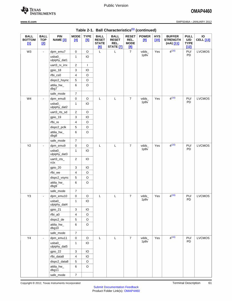
Public Version
OMAP4460
www.ti.com SWPS046A –JANUARY 2012
Table 2-1. Ball Characteristics(1) (continued)
BALL BALL PIN MODE TYPE BALL BALL RESET POWER HYS BUFFER PULL IOBOTTOM TOP NAME [3] [4] [5] RESET RESET REL. [9] [10] STRENGTH U/D CELL [13]
[1] [2] STATE REL. MODE (mA) [11] TYPE[6] STATE [7] [8] [12]
W3 - dpm_emu7 0 O L L 7 vdds_ Yes 4(16) PU/ LVCMOS1p8v PDusba0_ 1 IO
ulpiphy_dat1
uart3_rx_irrx 2 I
gpio_18 3 IO
rfbi_cs0 4 O
dispc2_hsync 5 O
attila_hw_ 6 Odbg7
safe_mode 7
W4 - dpm_emu8 0 O L L 7 vdds_ Yes 4(16) PU/ LVCMOS1p8v PDusba0_ 1 IO
ulpiphy_dat2
uart3_rts_sd 2 O
gpio_19 3 IO
rfbi_re 4 O
dispc2_pclk 5 O
attila_hw_ 6 Odbg8
safe_mode 7
Y2 - dpm_emu9 0 O L L 7 vdds_ Yes 4(16) PU/ LVCMOS1p8v PDusba0_ 1 IO
ulpiphy_dat3
uart3_cts_ 2 IOrctx
gpio_20 3 IO
rfbi_we 4 O
dispc2_vsync 5 O
attila_hw_ 6 Odbg9
safe_mode 7
Y3 - dpm_emu10 0 O L L 7 vdds_ Yes 4(16) PU/ LVCMOS1p8v PDusba0_ 1 IO
ulpiphy_dat4
gpio_21 3 IO
rfbi_a0 4 O
dispc2_de 5 O
attila_hw_ 6 Odbg10
safe_mode 7
Y4 - dpm_emu11 0 O L L 7 vdds_ Yes 4(16) PU/ LVCMOS1p8v PDusba0_ 1 IO
ulpiphy_dat5
gpio_22 3 IO
rfbi_data8 4 IO
dispc2_data8 5 O
attila_hw_ 6 Odbg11
safe_mode 7
Copyright © 2012, Texas Instruments Incorporated Terminal Description 61Submit Documentation Feedback
Product Folder Link(s): OMAP4460
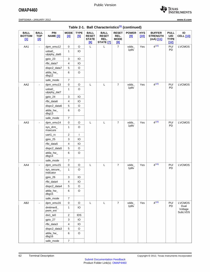
Public Version
OMAP4460
SWPS046A –JANUARY 2012 www.ti.com
Table 2-1. Ball Characteristics(1) (continued)
BALL BALL PIN MODE TYPE BALL BALL RESET POWER HYS BUFFER PULL IOBOTTOM TOP NAME [3] [4] [5] RESET RESET REL. [9] [10] STRENGTH U/D CELL [13]
[1] [2] STATE REL. MODE (mA) [11] TYPE[6] STATE [7] [8] [12]
AA1 - dpm_emu12 0 O L L 7 vdds_ Yes 4(16) PU/ LVCMOS1p8v PDusba0_ 1 IO
ulpiphy_dat6
gpio_23 3 IO
rfbi_data7 4 IO
dispc2_data7 5 O
attila_hw_ 6 Odbg12
safe_mode 7
AA2 - dpm_emu13 0 O L L 7 vdds_ Yes 4(16) PU/ LVCMOS1p8v PDusba0_ 1 O
ulpiphy_dat7
gpio_24 3 IO
rfbi_data6 4 IO
dispc2_data6 5 O
attila_hw_ 6 Odbg13
safe_mode 7
AA3 - dpm_emu14 0 O L L 7 vdds_ Yes 4(16) PU/ LVCMOS1p8v PDsys_drm_ 1 O
msecure
uart1_rx 2 I
gpio_25 3 IO
rfbi_data5 4 IO
dispc2_data5 5 O
attila_hw_ 6 Odbg14
safe_mode 7
AA4 - dpm_emu15 0 O L L 7 vdds_ Yes 4(16) PU/ LVCMOS1p8v PDsys_secure_ 1 O
indicator
gpio_26 3 IO
rfbi_data4 4 IO
dispc2_data4 5 O
attila_hw_ 6 Odbg15
safe_mode 7
AB2 - dpm_emu16 0 O L L 7 vdds_ Yes 4(16) PU/ LVCMOS1p8v PD Dualdmtimer8_ 1 IO
Voltagepwm_evtSubLVDS
dsi1_te0 2 IDS
gpio_27 3 IO
rfbi_data3 4 IO
dispc2_data3 5 O
attila_hw_ 6 Odbg16
safe_mode 7
62 Terminal Description Copyright © 2012, Texas Instruments Incorporated
Submit Documentation FeedbackProduct Folder Link(s): OMAP4460

Public Version
OMAP4460
www.ti.com SWPS046A –JANUARY 2012
Table 2-1. Ball Characteristics(1) (continued)
BALL BALL PIN MODE TYPE BALL BALL RESET POWER HYS BUFFER PULL IOBOTTOM TOP NAME [3] [4] [5] RESET RESET REL. [9] [10] STRENGTH U/D CELL [13]
[1] [2] STATE REL. MODE (mA) [11] TYPE[6] STATE [7] [8] [12]
AB3 - dpm_emu17 0 O L L 7 vdds_ Yes 4(16) PU/ LVCMOS1p8v PD Dualdmtimer9_ 1 IO
Voltagepwm_evtSubLVDS
dsi1_te1 2 IDS
gpio_28 3 IO
rfbi_data2 4 IO
dispc2_data2 5 O
attila_hw_ 6 Odbg17
safe_mode 7
AB4 - dpm_emu18 0 O L L 7 vdds_ Yes 4(16) PU/ LVCMOS1p8v PD Dualdmtimer10_ 1 IO
Voltagepwm_evtSubLVDS
dsi2_te0 2 IDS
gpio_190 3 IO
rfbi_data1 4 IO
dispc2_data1 5 O
attila_hw_ 6 Odbg18
safe_mode 7
AC4 - dpm_emu19 0 O L L 7 vdds_ Yes 4(16) PU/ LVCMOS1p8v PD Dualdmtimer11_ 1 IO
Voltagepwm_evtSubLVDS
dsi2_te1 2 IDS
gpio_191 3 IO
rfbi_data0 4 IO
dispc2_data0 5 O
attila_hw_ 6 Odbg19
safe_mode 7
Copyright © 2012, Texas Instruments Incorporated Terminal Description 63Submit Documentation Feedback
Product Folder Link(s): OMAP4460

Public Version
OMAP4460
SWPS046A –JANUARY 2012 www.ti.com
Table 2-1. Ball Characteristics(1) (continued)
BALL BALL PIN MODE TYPE BALL BALL RESET POWER HYS BUFFER PULL IOBOTTOM TOP NAME [3] [4] [5] RESET RESET REL. [9] [10] STRENGTH U/D CELL [13]
[1] [2] STATE REL. MODE (mA) [11] TYPE[6] STATE [7] [8] [12]
H1 / M1 / A2 / vss - GND NA NA NA NA NA NA NA NAAB1 / C2 / A6 /F2 / K2 / A9 /
U2 / AF2 / A11 /B3 / J3 / A14 /
J4 / AG4 / A28 /B6 / K8 / B1 /
U8 / AH8 / B14 /N9 / A10 / B21 /
AH10 / B24 /H11 / B29 /
AA11 / E28 /N12 / P12 F1 /
/ R12 / H28 /T12 / U12 J1 // AA12 / L29 /
B13 / H13 M2 // M13 / P1 /
N13 / P13 P2 // R13 / R28 /
T13 / U13 V2 // AH13 / V28 /
M14 / N14 AA28 // P14 / AB2 /
R14 / T14 AE2 // U14 / AF28 /
M15 / N15 AH1 // P15 / AH5 /
R15 / T15 AH14/ U15 / /
M16 / N16 AH18/ P16 / /
R16 / T16 AH29/ U16 / / AJ2 /
H17 / M17 AJ7 // N17 / AJ11 /
P17 / R17 AJ16 // T17 / AJ22 /
U17 / Y17 AJ28/ AG17 /
H19 / A20/ AA20 /
J21 / L21 /M21 / U21/ AH21 /
M22 / A23/ F25 / L25/ Y25 / L26
/ Y26 /AG26 /B27 /
AE27 /H28 / K28
/ U28
Y22 - vpp(20) - PWR NA NA NA NA NA NA NA NA
J8 - vpp_cust(20) - PWR NA NA NA NA NA NA NA NA
64 Terminal Description Copyright © 2012, Texas Instruments Incorporated
Submit Documentation FeedbackProduct Folder Link(s): OMAP4460
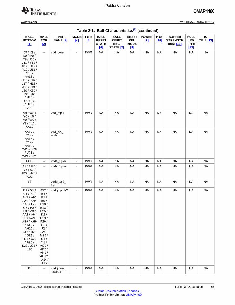
Public Version
OMAP4460
www.ti.com SWPS046A –JANUARY 2012
Table 2-1. Ball Characteristics(1) (continued)
BALL BALL PIN MODE TYPE BALL BALL RESET POWER HYS BUFFER PULL IOBOTTOM TOP NAME [3] [4] [5] RESET RESET REL. [9] [10] STRENGTH U/D CELL [13]
[1] [2] STATE REL. MODE (mA) [11] TYPE[6] STATE [7] [8] [12]
J9 / K9 / - vdd_core - PWR NA NA NA NA NA NA NA NAL9 / M9 /T9 / J10 /
J11 / Y11 /H12 / J12 /Y12 / J13 /
Y13 /AA13 /
J15 / J16 /J17 / H18 /J18 / J19 /J20 / K20 /L20 / M20
/ N20 /R20 / T20
/ U20 /V20
V8 / W8 / - vdd_mpu - PWR NA NA NA NA NA NA NA NAY8 / U9 /V9 / W9 /Y9 / Y10 /
AA10
AA17 / - vdd_iva_ - PWR NA NA NA NA NA NA NA NAY18 / audio
AA18 /Y19 /
AA19 /W20 / Y20
/ V21 /W21 / Y21
AA16 - vdds_1p2v - PWR NA NA NA NA NA NA NA NA
AB7 / U7 / - vdds_1p8v - PWR NA NA NA NA NA NA NA NAV7 / K7 /
H22 / J22 /W22
Y7 - vdds_1p8_ - PWR NA NA NA NA NA NA NA NAfref
D1 / G1 / A22 / vddq_lpddr2 - PWR NA NA NA NA NA NA NA NAU1 / Y1 / B4 /
AC1 / AF1 B7 // A4 / AH4 B9 // A6 / L7 / B13 /G8 / H8 / B18 /L8 / M8 / B25 /
AA8 / A9 / D2 /H9 / AA9 / D29 /AB9 / AH9 F29 /
/ A12 / G2 /AH12 / J2 /
A17 / H20 J28 // G21 / M28 /
H21 / A22 U1 // A25 / Y1 /
E28 / J28 / AC1 /L28 AF2 /
AH9 /AH12/ AJ4 /
AJ6
G15 - vddq_vref_ - PWR NA NA NA NA NA NA NA NAlpddr21
Copyright © 2012, Texas Instruments Incorporated Terminal Description 65Submit Documentation Feedback
Product Folder Link(s): OMAP4460
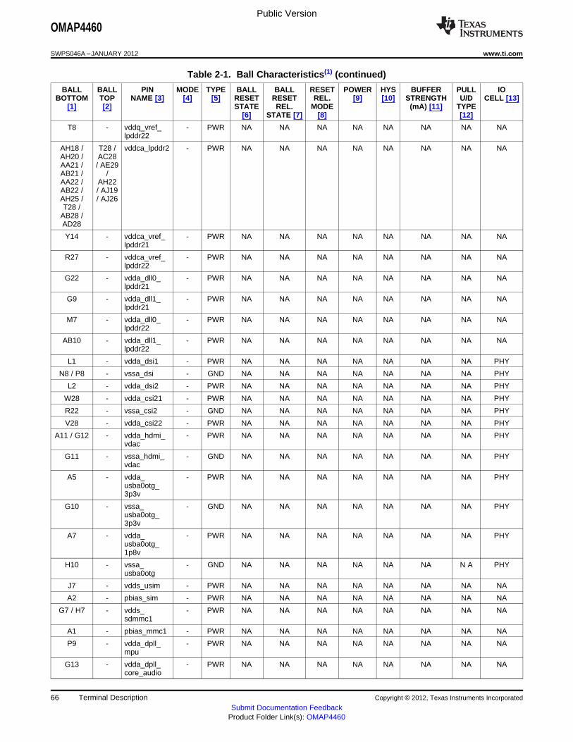
Public Version
OMAP4460
SWPS046A –JANUARY 2012 www.ti.com
Table 2-1. Ball Characteristics(1) (continued)
BALL BALL PIN MODE TYPE BALL BALL RESET POWER HYS BUFFER PULL IOBOTTOM TOP NAME [3] [4] [5] RESET RESET REL. [9] [10] STRENGTH U/D CELL [13]
[1] [2] STATE REL. MODE (mA) [11] TYPE[6] STATE [7] [8] [12]
T8 - vddq_vref_ - PWR NA NA NA NA NA NA NA NAlpddr22
AH18 / T28 / vddca_lpddr2 - PWR NA NA NA NA NA NA NA NAAH20 / AC28AA21 / / AE29AB21 / /AA22 / AH22AB22 / / AJ19AH25 / / AJ26T28 /
AB28 /AD28
Y14 - vddca_vref_ - PWR NA NA NA NA NA NA NA NAlpddr21
R27 - vddca_vref_ - PWR NA NA NA NA NA NA NA NAlpddr22
G22 - vdda_dll0_ - PWR NA NA NA NA NA NA NA NAlpddr21
G9 - vdda_dll1_ - PWR NA NA NA NA NA NA NA NAlpddr21
M7 - vdda_dll0_ - PWR NA NA NA NA NA NA NA NAlpddr22
AB10 - vdda_dll1_ - PWR NA NA NA NA NA NA NA NAlpddr22
L1 - vdda_dsi1 - PWR NA NA NA NA NA NA NA PHY
N8 / P8 - vssa_dsi - GND NA NA NA NA NA NA NA PHY
L2 - vdda_dsi2 - PWR NA NA NA NA NA NA NA PHY
W28 - vdda_csi21 - PWR NA NA NA NA NA NA NA PHY
R22 - vssa_csi2 - GND NA NA NA NA NA NA NA PHY
V28 - vdda_csi22 - PWR NA NA NA NA NA NA NA PHY
A11 / G12 - vdda_hdmi_ - PWR NA NA NA NA NA NA NA PHYvdac
G11 - vssa_hdmi_ - GND NA NA NA NA NA NA NA PHYvdac
A5 - vdda_ - PWR NA NA NA NA NA NA NA PHYusba0otg_3p3v
G10 - vssa_ - GND NA NA NA NA NA NA NA PHYusba0otg_3p3v
A7 - vdda_ - PWR NA NA NA NA NA NA NA PHYusba0otg_1p8v
H10 - vssa_ - GND NA NA NA NA NA NA N A PHYusba0otg
J7 - vdds_usim - PWR NA NA NA NA NA NA NA NA
A2 - pbias_sim - PWR NA NA NA NA NA NA NA NA
G7 / H7 - vdds_ - PWR NA NA NA NA NA NA NA NAsdmmc1
A1 - pbias_mmc1 - PWR NA NA NA NA NA NA NA NA
P9 - vdda_dpll_ - PWR NA NA NA NA NA NA NA NAmpu
G13 - vdda_dpll_ - PWR NA NA NA NA NA NA NA NAcore_audio
66 Terminal Description Copyright © 2012, Texas Instruments Incorporated
Submit Documentation FeedbackProduct Folder Link(s): OMAP4460

Public Version
OMAP4460
www.ti.com SWPS046A –JANUARY 2012
Table 2-1. Ball Characteristics(1) (continued)
BALL BALL PIN MODE TYPE BALL BALL RESET POWER HYS BUFFER PULL IOBOTTOM TOP NAME [3] [4] [5] RESET RESET REL. [9] [10] STRENGTH U/D CELL [13]
[1] [2] STATE REL. MODE (mA) [11] TYPE[6] STATE [7] [8] [12]
Y16 - vdda_dpll_ - PWR NA NA NA NA NA NA NA NAiva_per
G20 - vdds_dv_ - PWR NA NA NA NA NA NA NA NAgpmc
G16 / H16 - vdds_dv_ - PWR NA NA NA NA NA NA NA NAsdmmc2
G17 / G18 - vdds_dv_c2c - PWR NA NA NA NA NA NA NA NA/ G19
V22 - vdds_dv_cam - PWR NA NA NA NA NA NA NA NA
AB16 - vdds_dv_ - PWR NA NA NA NA NA NA NA NAbank0
AB20 - vdds_dv_ - PWR NA NA NA NA NA NA NA NAbank1
AB8 / - vdds_dv_ - PWR NA NA NA NA NA NA NA NAAB19 bank2
AB18 - vdds_dv_ - PWR NA NA NA NA NA NA NA NAbank3
AA7 - vdds_dv_ - PWR NA NA NA NA NA NA NA NAbank4
AB17 - vdds_dv_ - PWR NA NA NA NA NA NA NA NAbank5
AA14 - vdds_dv_ - PWR NA NA NA NA NA NA NA NAbank6
M28 - vdds_dv_ - PWR NA NA NA NA NA NA NA NAbank7
W7 - vdds_dv_fref - PWR NA NA NA NA NA NA NA NA
AB14 - vdda_ldo_ - PWR NA NA NA NA NA NA NA NAsram_mpu
N22 - vdda_ldo_ - PWR NA NA NA NA NA NA NA NAsram_iva_audio
T22 - vdda_ldo_ - PWR NA NA NA NA NA NA NA NAsram_core
P7 - vdda_ldo_ - PWR NA NA NA NA NA NA NA NAemu_wkup
AB12 - vdda_bdgp_ - PWR NA NA NA NA NA NA NA NAvbb
AB13 - cap_vbb_ldo - PWR NA NA NA NA NA NA NA NA_mpu
R21 - cap_vbb_ldo - PWR NA NA NA NA NA NA NA NA_iva_audio
AB11 - cap_vdd_ldo - PWR NA NA NA NA NA NA NA NA_sram_mpu
N21 - cap_vdd_ldo - PWR NA NA NA NA NA NA NA NA_sram_iva_audio
U22 - cap_vdd_ldo - PWR NA NA NA NA NA NA NA NA_sram_core
T7 - cap_vdd_ldo - PWR NA NA NA NA NA NA NA NA_emu_wkup
A27 - atestv - AO Z NA 0 vdds_ NA NA NA Analog1p8v
AG28 - vsense - AO Z NA 0 NA NA NA NA Analog
Copyright © 2012, Texas Instruments Incorporated Terminal Description 67Submit Documentation Feedback
Product Folder Link(s): OMAP4460

Public Version
OMAP4460
SWPS046A –JANUARY 2012 www.ti.com
Table 2-1. Ball Characteristics(1) (continued)
BALL BALL PIN MODE TYPE BALL BALL RESET POWER HYS BUFFER PULL IOBOTTOM TOP NAME [3] [4] [5] RESET RESET REL. [9] [10] STRENGTH U/D CELL [13]
[1] [2] STATE REL. MODE (mA) [11] TYPE[6] STATE [7] [8] [12]
AH27 - iforce - AI Z NA 0 NA No NA No Analog
AH16 AJ17 pop_lpddr21_ - FEED NA NA NA NA NA NA NA NAzq
AF28 AG29 pop_lpddr22_ - FEED NA NA NA NA NA NA NA NAzq
A26 / B2 B2 / pop_vacc_ - PWR NA NA NA NA NA NA NA NAB28 lpddr2
AG27 / C1 C1 / pop_vdd1_ - PWR NA NA NA NA NA NA NA NA/ AG2 AH2 / lpddr2_
AH28 shared
A13 / C27 A15 / pop_vdd1_ - PWR NA NA NA NA NA NA NA NA/ AH14 C28 / lpddr21
AJ15
N1 / P1 / N2 / pop_vdd1_ - PWR NA NA NA NA NA NA NA NAR28 P29 / lpddr22
R1
AH3 / A3 / A3 / pop_vdd2_ - PWR NA NA NA NA NA N A NA NAC28 / C29 / lpddr2_AF27 AG28 shared
/ AH3
AG14 / A16 / pop_vdd2_ - PWR NA NA NA NA NA NA NA NAA15 / B15 B16 / lpddr21
AH15
N28 / T1 / P28 / pop_vdd2_ - PWR NA NA NA NA NA NA NA NAT2 T1 / lpddr22
T2
(1) NA stands for Not Applicable.
(2) x and y = 20 to 70 µA
(3) x and y = 40 to 70 µA
(4) The cell is provided with the flexibility of selecting optimal voltage level based on the current load requirement among 2 µA, 4 µA, 6 µA,or 8 µA.
(5) The pullup or pulldown can be either the standard LVCMOS 100-μA drive strength or the configurable I2C internal pullup resistances.The default buffer configuration is the following:
– PUx/PDy-OD is specified: the default buffer configuration is High-Speed I2C point-to-point mode using internal pullup resistance.– PUx/PDy-GPIO is specified: the default buffer configuration is standard LVCMOS mode (non-I2C). The internal pullup resistance
programming does not apply in this mode.
In I2C mode configuration, for a full description of the internal pullup resistance programming according to the load range, see theCONTROL_I2C_0 and CONTROL_I2C_2 registers in the Control Module / Control Module Functional Description / Functional RegisterDescription / Signal Integrity Parameter Control Registers With Pad Group Assignment section of the OMAP4460 TRM.In standard LVCMOS mode configuration (non-I2C mode), for a full description of the pullup or pulldown programming, see theCONTROL_CORE_PADX registers in the Control Module / Control Module Functional Description / Pad Functional Multiplexing andConfiguration section of the OMAP4460 TRM.
(6) The drive strength is fixed regardless of the load. The driver is designed to drive 75 Ω for video applications.
(7) In buffer mode, the drive strength is fixed regardless of the load. The driver is designed to drive 75 Ω for video applications. In bypassmode, the drive strength is 0.47 mA.
(8) PAD can be driven low or high impedance by the driver. External pullup is required and can vary between 1 kΩ and 10 kΩ. The circuitrypulling up or pulling down the pad must be able to provide at least 100 µA of current without collapsing.
(9) PD: 30 kΩ to 150 kΩ. PU: 50 kΩ to 110 kΩ(10) PD resistance: from 30 kΩ to 150 kΩ.
The pullup resistance is configurable by software programming:
– PUSTRENGTH = 1: PU resistance from 10 kΩ to 50 kΩ– PUSTRENGTH = 0: PU resistance from 50 kΩ to 110 kΩFor more information regarding the PUSTRENGTH programming, see the Control Module / Control Module Functional Description /Functional Register Description / Signal Integrity Parameter Control Registers With Pad Group Assignment / SDMMC1 Pullup StrengthControl section of the OMAP4460 TRM.
(11) The maximum capacitive load for the DSI low-power mode is equal to 60 pF. See Chapter 8 of the MIPI D-PHY standard v1.0 for
68 Terminal Description Copyright © 2012, Texas Instruments Incorporated
Submit Documentation FeedbackProduct Folder Link(s): OMAP4460
Public Version
OMAP4460
www.ti.com SWPS046A –JANUARY 2012
complete specification on the electrical characteristics.No specific capacitive load is needed in DSI high-speed mode.The PCB interconnect must be 50-Ω transmission line on DSI dsi_dx[2;0] and DSI dsi_dy[2;0]. DSI dsi_dx[2;0] and DSI dsi_dy[2;0] linesmust be well matched. See Chapter 7 of the MIPI D-PHY standard v1.0 for complete specification of the interconnect.
(12) The buffer strength of this IO cell is programmable (2.5, 5, 7.5, or 10 mA); the default value is described in the table above.
(13) IO drive strength for D+ (usba0_otg_dp) and D– (usba0_otg_dm): minimum 18.3 mA, maximum 89 mA (for a power supplyvdda_usba0otg_3p3v = 3.6 V).Ball characteristics are compliant with USB2.0.
(14) PU = minimum 900 Ω, maximum 3.090 kΩ and PD = minimum 14.25 kΩ, maximum 24.8 kΩ. Note that:
– PU is typically connected for D+ (usba0_otg_dp) in Full Speed mode and for D– (usba0_otg_dm) in Low Speed mode.– PD is typically connected for D+ (usba0_otg_dp) and D– (usba0_otg_dm) whatever the modes. PD is connected to both D+ and D–
only if OMAP4 is used as HOST.Ball characteristics are compliant with USB2.0.
(15) For H2 / H3 / H4 / D2 / E3 / E4 / E2 / E1 / F4 / F3 / F1 / G2 / G4 / G3 / J2 balls, the hysteresis value is equal to 100 mV minimum for1.8 V (vdds_mmc1 or vdds_usim following the interface used), or 50 mV minimum for 3.0 V (vdds_mmc1 or vdds_usim following theinterface used).
(16) The buffer drive strength is configurable by software programming:
– Mode 2: DS0 = 0, impedance = 50 Ω (buffer drive strength = 4 mA, IOL = IOH = 4 mA)– Mode 1: DS0 = 1, impedance = 25 Ω (buffer drive strength = 8 mA, IOL = IOH = 8 mA)In the BUFFER STRENGTH (mA) [11] column is defined the value by default.For more information regarding the DS0 programming, see the CONTROL_SMART2IO_PADCONF_2 register in the Control Module /Control Module Functional Description / Functional Register Description / Signal Integrity Parameter Control Registers With Pad GroupAssignment section of the OMAP4460 TRM.For more information regarding the load, rise / fall times vs frequency depending the modes (DS0 = 0 or 1) or the supply voltage value(1.2-V or 1.8-V), see Table 3-4, GPMC DC Electrical Characteristics.
(17) For AE18 / AG12 balls, the hysteresis value is equal to 70 mV minimum for 1.8 V and 60 mV minimum for 1.2 V. For P2 / V2 balls, thehysteresis value is equal to 70 mV minimum for 1.8 V.
(18) For more information regarding the MIPI D-PHY hysteresis, see Section 3.3.3, Camera DC Electrical Characteristics, Section 3.3.4,Display DC Electrical Characteristics.
(19) For B5 / B4 balls, the hysteresis is:
– In low-speed and full-speed single-ended receiver modes: minimum 20 mV, typical 50 mV, maximum 80 mV– In differential receiver modes, no hysteresis feature is present.
(20) vpp must be unconnected. vpp_cust is only powered when programming CPFROM eFuses. Otherwise, it is recommended to leavevpp_cust turned off (floating). Note that if the TWL6030 PMIC is used then the vpp pulldown resistor inside the TWL6030 must bedisabled when the vpp_cust is turned off.
(21) IO drive strength for usba0_otg_ce pin: minimum 100 µA, maximum 20 mA.
(22) If a CSI2 serial PHY is enabled, vdda_csi2 must be supplied by a dedicated 1.8V low-noise power source.If a CSI2 serial PHY is definitively disabled, other multiplexed 1.8-V CMOS signals of the interface can be enabled, the interface can besupplied by the same power source as vdds_1p8v: the vdds_1p8v power source supplies vdda_csi2 ball.If CSI2 serial PHY and CMOS signals are definitively disabled, the interface balls are left unconnected with its associated power supply(vdda/vssa) grounded (for circuit reliability reasons).
(23) If a DSI serial PHY is enabled, vdda_dsi must be supplied by a dedicated 1.8-V low-noise power source.If a DSI serial PHY is definitively disabled, the interface balls are left unconnected and in that case the associated power supply(vdda/vssa) can be grounded (for circuit reliability reasons) only if the corresponding DSI DPLL is never used to generate the functionalclock to the DISPC.
(24) If the HDMI serial PHY is enabled, vdda_hdmi_vdac must be supplied by a dedicated 1.8-V low-noise power source.If the HDMI serial PHY is definitively disabled, the interface balls are left unconnected with its associated power supply (vdda/vssa)grounded (for circuit reliability reasons).
(25) If the HS USB OTG PHY is enabled, vdda_usba0otg_3p3v and vdda_usba0otg_1p8v must be supplied by dedicated 3.3-V and 1.8-Vlow-noise power sources.If the USB OTG PHY is definitively disabled, other multiplexed 3.3V CMOS signals of the interface can be enabled,vdda_usba0otg_3p3v must be supplied by a dedicated 3.3-V power source and vdda_usba0otg_1p8v can be supplied by the samepower source as vdds_1p8v.If the USB OTG PHY and CMOS signals are definitively disabled, vdda_usba0otg_3p3v and vdda_usba0otg_1p8v are grounded forpower saving and there is a forward-biased diode from usba0_otg_dp, usba0_otg_dm, usba0_otg_ce pins to vdda_usba0otg_3p3v pin.
(26) If the SDMMC1 functional signals are enabled, vdds_sdmmc1 must be supplied by either dedicated 1.8-V or 3.0-V power source.If the SDMMC1 functional signals are definitively disabled, other multiplexed 1.8-V CMOS signals of the interface can be enabled, theinterface can be supplied by the same power source as vdds_1p8v: the vdds_1p8v power source supplies vdds_sdmmc1.If the SDMMC1 functional balls and CMOS signals are definitively disabled, the interface balls are left unconnected andMMC1_PWRDNZ and MMC1_PBIASLITE_PWRDNZ bits are kept at 0. There are two options for the associated power supply:
– vdds_sdmmc1 is grounded.– vdds_sdmmc1 is supplied by a 1.8-V or 3.0-V supply. In this case, it is also recommended to keep default value of
MMC1_PBIASLITE_VMODE bit (that is, 1).
For the corresponding setting of the MMC1_PWRDNZ, MMC1_PBIASLITE_PWRDNZ, and MMC1_PBIASLITE_VMODE bits, see the
Copyright © 2012, Texas Instruments Incorporated Terminal Description 69Submit Documentation Feedback
Product Folder Link(s): OMAP4460
Public Version
OMAP4460
SWPS046A –JANUARY 2012 www.ti.com
Control Module / Control Module Functional Description / Extended-Drain I/O and PBIAS Cell section and the Control Module / ControlModule Programming Guide section of the OMAP4460 TRM.
(27) If USIM, USBC1 functional signals are enabled, vdds_usim must be supplied by either dedicated 1.8-V or 3.0-V power source.If USIM, USBC1 functional signals are definitively disabled, other multiplexed 1.8-V CMOS signals of the interface can be enabled, theinterface can be supplied by the same power source as vdds_1p8v: the vdds_1p8v power source supplies vdds_usim ball.If the USIM, USBC1 functional balls and CMOS signals are definitively disabled, the interface balls are left unconnected andGPIOWK_IO_PWRDNZ, USBC1_ICUSB_PWRDNZ, and PBIASLITE1_PWRDNZ bits are kept at 0. There are two options for theassociated power supply:
– vdds_usim is grounded.– vdds_usim is supplied by a 1.8-V or 3.0-V supply. In this case, it is also recommended to keep default value of
PBIASLITE1_VMODE bit (that is, 1).
For the corresponding setting of the GPIOWK_IO_PWRDNZ, USBC1_ICUSB_PWRDNZ, PBIASLITE1_PWRDNZ, andPBIASLITE1_VMODE bits, see the Control Module / Control Module Functional Description / Extended-Drain I/O and PBIAS Cell sectionand the Control Module / Control Module Programming Guide section of the OMAP4460 TRM.
(28) In the device, the number “2” in the cam2 interface name does not mean there are two camera parallel interfaces available in thedevice. The cam2 interface name defines the camera parallel interface available in the device vs the legacy device.
(29) The function (data or clock) supported on each lane is programmable. For more information on HDMI, please contact your TIrepresentative.
(30) The HDMI pulldown resistor is only enabled when the HDMI supply is either ramping or off. Hence, this pulldown resistor is not linkedto the HDMI standard protocol.
2.3 Multiplexing Characteristics
Table 2-2 describes the device multiplexing (no characteristics are available in this table).
NOTEThis table doesn't take into account subsystem multiplexing signals. Subsystem multiplexingsignals are described in Section 2.4, Signal Descriptions.
NOTEFor more information, see the Control Module / Control Module Functional Description / PADFunctional Multiplexing and Configuration section of the OMAP4460 TRM.
NOTEConfiguring two pins to the same input signal is not supported as it can yield unexpectedresults. This can be easily prevented with the proper software configuration. (safe_mode isnot an input signal.)
NOTEWhen a pad is set into a multiplexing mode which is not defined by pin multiplexing, this padis actually set undriven (HiZ) with potential pullup / pulldown. Pulls need to be disabled tohave a pure HiZ.
NOTEAll balls not described in Table 2-1 and Table 2-2 are not connected.
Table 2-2. Multiplexing Characteristics(1)
BALL BALL Mode 0 Mode 1 Mode 2 Mode 3 Mode 4 Mode 5 Mode 6 Mode 7BOTTOM TOP
C12 - gpmc_ad0 sdmmc2_ - - - - - -dat0
D12 - gpmc_ad1 sdmmc2_ - - - - - -dat1
70 Terminal Description Copyright © 2012, Texas Instruments Incorporated
Submit Documentation FeedbackProduct Folder Link(s): OMAP4460
Public Version
OMAP4460
www.ti.com SWPS046A –JANUARY 2012
Table 2-2. Multiplexing Characteristics(1) (continued)
BALL BALL Mode 0 Mode 1 Mode 2 Mode 3 Mode 4 Mode 5 Mode 6 Mode 7BOTTOM TOP
C13 - gpmc_ad2 sdmmc2_ - - - - - -dat2
D13 - gpmc_ad3 sdmmc2_ - - - - - -dat3
C15 - gpmc_ad4 sdmmc2_ sdmmc2_dir - - - - -dat4 _dat0
D15 - gpmc_ad5 sdmmc2_ sdmmc2_dir - - - - -dat5 _dat1
A16 - gpmc_ad6 sdmmc2_ sdmmc2_dir - - - - -dat6 _cmd
B16 - gpmc_ad7 sdmmc2_ sdmmc2_clk - - - - -dat7 _fdbk
C16 - gpmc_ad8 kpd_row0 - gpio_32 - sdmmc1_ - -dat0
D16 - gpmc_ad9 kpd_row1 - gpio_33 - sdmmc1_ - -dat1
C17 - gpmc_ad10 kpd_row2 - gpio_34 - sdmmc1_ - -dat2
D17 - gpmc_ad11 kpd_row3 - gpio_35 - sdmmc1_ - -dat3
C18 - gpmc_ad12 kpd_col0 - gpio_36 - sdmmc1_ - -dat4
D18 - gpmc_ad13 kpd_col1 - gpio_37 - sdmmc1_ - -dat5
C19 - gpmc_ad14 kpd_col2 - gpio_38 - sdmmc1_ - -dat6
D19 - gpmc_ad15 kpd_col3 - gpio_39 - sdmmc1_ - -dat7
B17 - gpmc_a16 kpd_row4 - gpio_40 venc_656_ - - safe_modedata0
A18 - gpmc_a17 kpd_row5 - gpio_41 venc_656_ - - safe_modedata1
B18 - gpmc_a18 kpd_row6 - gpio_42 venc_656_ - - safe_modedata2
A19 - gpmc_a19 kpd_row7 - gpio_43 venc_656_ - - safe_modedata3
B19 - gpmc_a20 kpd_col4 - gpio_44 venc_656_ - - safe_modedata4
B20 - gpmc_a21 kpd_col5 - gpio_45 venc_656_ - - safe_modedata5
A21 - gpmc_a22 kpd_col6 - gpio_46 venc_656_ - - safe_modedata6
B21 - gpmc_a23 kpd_col7 - gpio_47 venc_656_ - - safe_modedata7
C20 - gpmc_a24 kpd_col8 - gpio_48 - - - safe_mode
D20 - gpmc_a25 - - gpio_49 - - - safe_mode
B25 - gpmc_ncs0 - - gpio_50 sys_ - - -ndmareq0
C21 - gpmc_ncs1 - - gpio_51 - - - safe_mode
D21 - gpmc_ncs2 kpd_row8 - gpio_52 - - - safe_mode
C22 - gpmc_ncs3 gpmc_dir - gpio_53 - - - safe_mode
C25 - gpmc_nwp dsi1_te0 - gpio_54 sys_ - - -ndmareq1
Copyright © 2012, Texas Instruments Incorporated Terminal Description 71Submit Documentation Feedback
Product Folder Link(s): OMAP4460
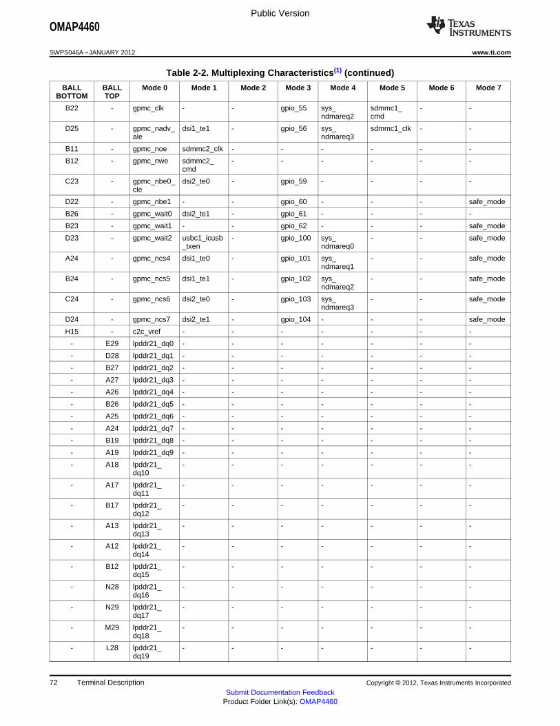
Public Version
OMAP4460
SWPS046A –JANUARY 2012 www.ti.com
Table 2-2. Multiplexing Characteristics(1) (continued)
BALL BALL Mode 0 Mode 1 Mode 2 Mode 3 Mode 4 Mode 5 Mode 6 Mode 7BOTTOM TOP
B22 - gpmc_clk - - gpio_55 sys_ sdmmc1_ - -ndmareq2 cmd
D25 - gpmc_nadv_ dsi1_te1 - gpio_56 sys_ sdmmc1_clk - -ale ndmareq3
B11 - gpmc_noe sdmmc2_clk - - - - - -
B12 - gpmc_nwe sdmmc2_ - - - - - -cmd
C23 - gpmc_nbe0_ dsi2_te0 - gpio_59 - - - -cle
D22 - gpmc_nbe1 - - gpio_60 - - - safe_mode
B26 - gpmc_wait0 dsi2_te1 - gpio_61 - - - -
B23 - gpmc_wait1 - - gpio_62 - - - safe_mode
D23 - gpmc_wait2 usbc1_icusb - gpio_100 sys_ - - safe_mode_txen ndmareq0
A24 - gpmc_ncs4 dsi1_te0 - gpio_101 sys_ - - safe_modendmareq1
B24 - gpmc_ncs5 dsi1_te1 - gpio_102 sys_ - - safe_modendmareq2
C24 - gpmc_ncs6 dsi2_te0 - gpio_103 sys_ - - safe_modendmareq3
D24 - gpmc_ncs7 dsi2_te1 - gpio_104 - - - safe_mode
H15 - c2c_vref - - - - - - -
- E29 lpddr21_dq0 - - - - - - -
- D28 lpddr21_dq1 - - - - - - -
- B27 lpddr21_dq2 - - - - - - -
- A27 lpddr21_dq3 - - - - - - -
- A26 lpddr21_dq4 - - - - - - -
- B26 lpddr21_dq5 - - - - - - -
- A25 lpddr21_dq6 - - - - - - -
- A24 lpddr21_dq7 - - - - - - -
- B19 lpddr21_dq8 - - - - - - -
- A19 lpddr21_dq9 - - - - - - -
- A18 lpddr21_ - - - - - - -dq10
- A17 lpddr21_ - - - - - - -dq11
- B17 lpddr21_ - - - - - - -dq12
- A13 lpddr21_ - - - - - - -dq13
- A12 lpddr21_ - - - - - - -dq14
- B12 lpddr21_ - - - - - - -dq15
- N28 lpddr21_ - - - - - - -dq16
- N29 lpddr21_ - - - - - - -dq17
- M29 lpddr21_ - - - - - - -dq18
- L28 lpddr21_ - - - - - - -dq19
72 Terminal Description Copyright © 2012, Texas Instruments Incorporated
Submit Documentation FeedbackProduct Folder Link(s): OMAP4460
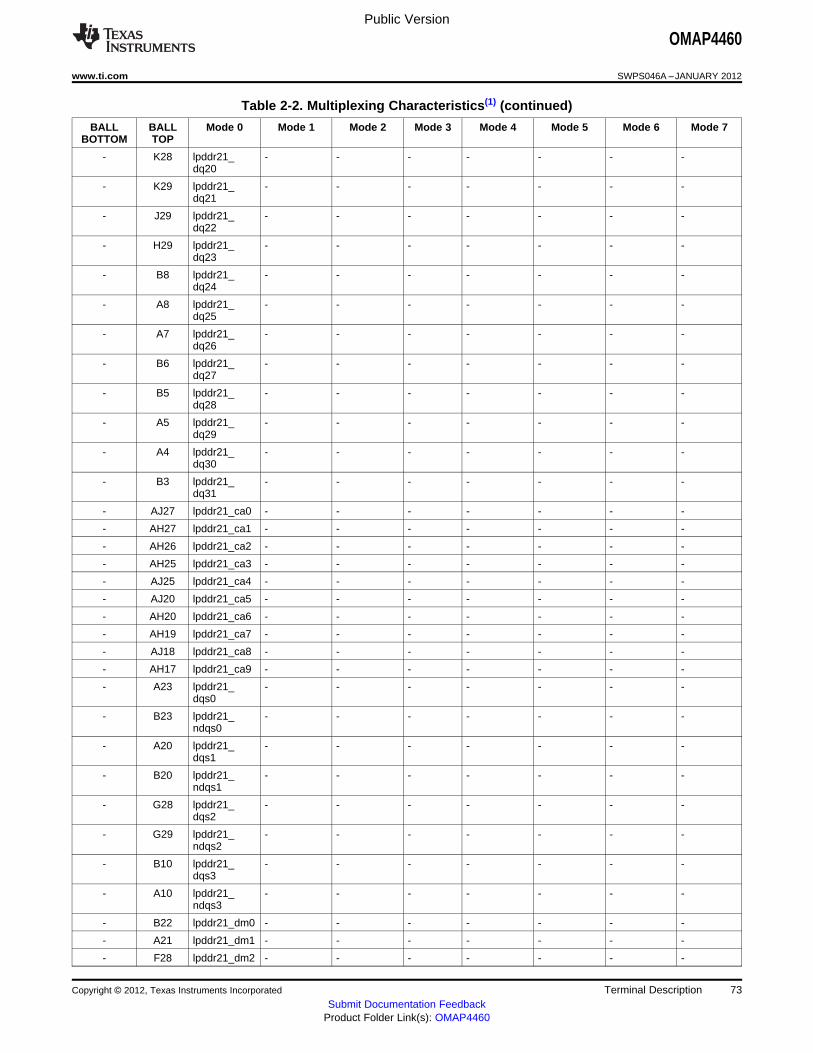
Public Version
OMAP4460
www.ti.com SWPS046A –JANUARY 2012
Table 2-2. Multiplexing Characteristics(1) (continued)
BALL BALL Mode 0 Mode 1 Mode 2 Mode 3 Mode 4 Mode 5 Mode 6 Mode 7BOTTOM TOP
- K28 lpddr21_ - - - - - - -dq20
- K29 lpddr21_ - - - - - - -dq21
- J29 lpddr21_ - - - - - - -dq22
- H29 lpddr21_ - - - - - - -dq23
- B8 lpddr21_ - - - - - - -dq24
- A8 lpddr21_ - - - - - - -dq25
- A7 lpddr21_ - - - - - - -dq26
- B6 lpddr21_ - - - - - - -dq27
- B5 lpddr21_ - - - - - - -dq28
- A5 lpddr21_ - - - - - - -dq29
- A4 lpddr21_ - - - - - - -dq30
- B3 lpddr21_ - - - - - - -dq31
- AJ27 lpddr21_ca0 - - - - - - -
- AH27 lpddr21_ca1 - - - - - - -
- AH26 lpddr21_ca2 - - - - - - -
- AH25 lpddr21_ca3 - - - - - - -
- AJ25 lpddr21_ca4 - - - - - - -
- AJ20 lpddr21_ca5 - - - - - - -
- AH20 lpddr21_ca6 - - - - - - -
- AH19 lpddr21_ca7 - - - - - - -
- AJ18 lpddr21_ca8 - - - - - - -
- AH17 lpddr21_ca9 - - - - - - -
- A23 lpddr21_ - - - - - - -dqs0
- B23 lpddr21_ - - - - - - -ndqs0
- A20 lpddr21_ - - - - - - -dqs1
- B20 lpddr21_ - - - - - - -ndqs1
- G28 lpddr21_ - - - - - - -dqs2
- G29 lpddr21_ - - - - - - -ndqs2
- B10 lpddr21_ - - - - - - -dqs3
- A10 lpddr21_ - - - - - - -ndqs3
- B22 lpddr21_dm0 - - - - - - -
- A21 lpddr21_dm1 - - - - - - -
- F28 lpddr21_dm2 - - - - - - -
Copyright © 2012, Texas Instruments Incorporated Terminal Description 73Submit Documentation Feedback
Product Folder Link(s): OMAP4460
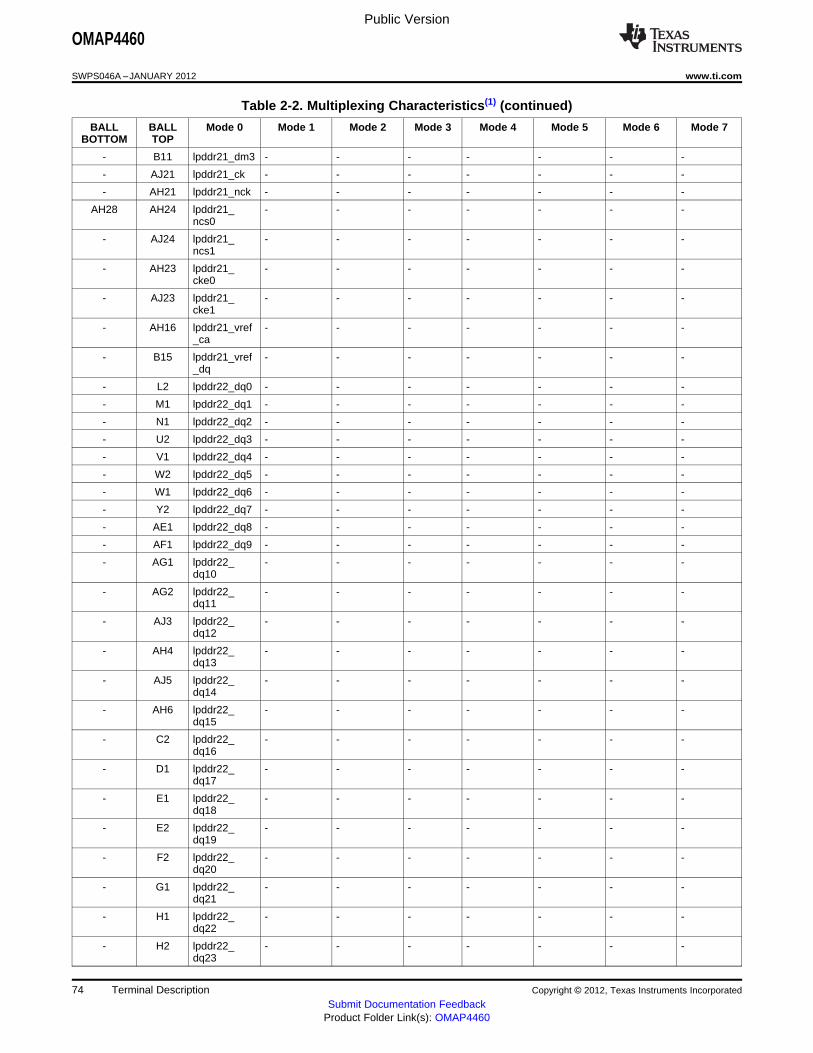
Public Version
OMAP4460
SWPS046A –JANUARY 2012 www.ti.com
Table 2-2. Multiplexing Characteristics(1) (continued)
BALL BALL Mode 0 Mode 1 Mode 2 Mode 3 Mode 4 Mode 5 Mode 6 Mode 7BOTTOM TOP
- B11 lpddr21_dm3 - - - - - - -
- AJ21 lpddr21_ck - - - - - - -
- AH21 lpddr21_nck - - - - - - -
AH28 AH24 lpddr21_ - - - - - - -ncs0
- AJ24 lpddr21_ - - - - - - -ncs1
- AH23 lpddr21_ - - - - - - -cke0
- AJ23 lpddr21_ - - - - - - -cke1
- AH16 lpddr21_vref - - - - - - -_ca
- B15 lpddr21_vref - - - - - - -_dq
- L2 lpddr22_dq0 - - - - - - -
- M1 lpddr22_dq1 - - - - - - -
- N1 lpddr22_dq2 - - - - - - -
- U2 lpddr22_dq3 - - - - - - -
- V1 lpddr22_dq4 - - - - - - -
- W2 lpddr22_dq5 - - - - - - -
- W1 lpddr22_dq6 - - - - - - -
- Y2 lpddr22_dq7 - - - - - - -
- AE1 lpddr22_dq8 - - - - - - -
- AF1 lpddr22_dq9 - - - - - - -
- AG1 lpddr22_ - - - - - - -dq10
- AG2 lpddr22_ - - - - - - -dq11
- AJ3 lpddr22_ - - - - - - -dq12
- AH4 lpddr22_ - - - - - - -dq13
- AJ5 lpddr22_ - - - - - - -dq14
- AH6 lpddr22_ - - - - - - -dq15
- C2 lpddr22_ - - - - - - -dq16
- D1 lpddr22_ - - - - - - -dq17
- E1 lpddr22_ - - - - - - -dq18
- E2 lpddr22_ - - - - - - -dq19
- F2 lpddr22_ - - - - - - -dq20
- G1 lpddr22_ - - - - - - -dq21
- H1 lpddr22_ - - - - - - -dq22
- H2 lpddr22_ - - - - - - -dq23
74 Terminal Description Copyright © 2012, Texas Instruments Incorporated
Submit Documentation FeedbackProduct Folder Link(s): OMAP4460

Public Version
OMAP4460
www.ti.com SWPS046A –JANUARY 2012
Table 2-2. Multiplexing Characteristics(1) (continued)
BALL BALL Mode 0 Mode 1 Mode 2 Mode 3 Mode 4 Mode 5 Mode 6 Mode 7BOTTOM TOP
- AJ9 lpddr22_ - - - - - - -dq24
- AJ10 lpddr22_ - - - - - - -dq25
- AH10 lpddr22_ - - - - - - -dq26
- AH11 lpddr22_ - - - - - - -dq27
- AJ12 lpddr22_ - - - - - - -dq28
- AJ13 lpddr22_ - - - - - - -dq29
- AH13 lpddr22_ - - - - - - -dq30
- AJ14 lpddr22_ - - - - - - -dq31
- R29 lpddr22_ca0 - - - - - - -
- T29 lpddr22_ca1 - - - - - - -
- U29 lpddr22_ca2 - - - - - - -
- V29 lpddr22_ca3 - - - - - - -
- W28 lpddr22_ca4 - - - - - - -
- AC29 lpddr22_ca5 - - - - - - -
- AD29 lpddr22_ca6 - - - - - - -
- AD28 lpddr22_ca7 - - - - - - -
- AE28 lpddr22_ca8 - - - - - - -
- AF29 lpddr22_ca9 - - - - - - -
- AA1 lpddr22_ - - - - - - -dqs0
- AA2 lpddr22_ - - - - - - -ndqs0
- AD2 lpddr22_ - - - - - - -dqs1
- AD1 lpddr22_ - - - - - - -ndqs1
- K2 lpddr22_ - - - - - - -dqs2
- K1 lpddr22_ - - - - - - -ndqs2
- AH8 lpddr22_ - - - - - - -dqs3
- AJ8 lpddr22_ - - - - - - -ndqs3
- AB1 lpddr22_dm0 - - - - - - -
- AC2 lpddr22_dm1 - - - - - - -
- L1 lpddr22_dm2 - - - - - - -
- AH7 lpddr22_dm3 - - - - - - -
- AB28 lpddr22_ck - - - - - - -
- AB29 lpddr22_nck - - - - - - -
- Y28 lpddr22_ - - - - - - -ncs0
- W29 lpddr22_ - - - - - - -ncs1
Copyright © 2012, Texas Instruments Incorporated Terminal Description 75Submit Documentation Feedback
Product Folder Link(s): OMAP4460

Public Version
OMAP4460
SWPS046A –JANUARY 2012 www.ti.com
Table 2-2. Multiplexing Characteristics(1) (continued)
BALL BALL Mode 0 Mode 1 Mode 2 Mode 3 Mode 4 Mode 5 Mode 6 Mode 7BOTTOM TOP
- AA29 lpddr22_ - - - - - - -cke0
- Y29 lpddr22_ - - - - - - -cke1
- U28 lpddr22_vref - - - - - - -_ca
- R2 lpddr22_vref - - - - - - -_dq
P3 - dsi1_dx0 - - - - - - -
P4 - dsi1_dy0 - - - - - - -
N3 - dsi1_dx1 - - - - - - -
N4 - dsi1_dy1 - - - - - - -
M3 - dsi1_dx2 - - - - - - -
M4 - dsi1_dy2 - - - - - - -
L3 - dsi1_dx3 - - - - - - -
L4 - dsi1_dy3 - - - - - - -
K3 - dsi1_dx4 - - - - - - -
K4 - dsi1_dy4 - - - - - - -
T3 - dsi2_dx0 - - - - - - -
T4 - dsi2_dy0 - - - - - - -
U3 - dsi2_dx1 - - - - - - -
U4 - dsi2_dy1 - - - - - - -
V3 - dsi2_dx2 - - - - - - -
V4 - dsi2_dy2 - - - - - - -
B7 - cvideo_tvout - - - - - - -
C7 - cvideo_vfb - - - - - - -
D7 - cvideo_rset - - - - - - -
B9 - hdmi_hpd - - gpio_63 - - - safe_mode
B10 - hdmi_cec - - gpio_64 - - - safe_mode
A8 - hdmi_ddc_ - - gpio_65 - - - safe_modescl
B8 - hdmi_ddc_ - - gpio_66 - - - safe_modesda
C8 - hdmi_data2x - - - - - - -
D8 - hdmi_data2y - - - - - - -
C9 - hdmi_data1x - - - - - - -
D9 - hdmi_data1y - - - - - - -
C10 - hdmi_data0x - - - - - - -
D10 - hdmi_data0y - - - - - - -
C11 - hdmi_clockx - - - - - - -
D11 - hdmi_clocky - - - - - - -
R26 - csi21_dx0 - - gpi_67 - - - safe_mode
R25 - csi21_dy0 - - gpi_68 - - - safe_mode
T26 - csi21_dx1 - - gpi_69 - - - safe_mode
T25 - csi21_dy1 - - gpi_70 - - - safe_mode
U26 - csi21_dx2 - - gpi_71 - - - safe_mode
U25 - csi21_dy2 - - gpi_72 - - - safe_mode
V26 - csi21_dx3 cam2_d7(4) - gpi_73 - - - safe_mode
76 Terminal Description Copyright © 2012, Texas Instruments Incorporated
Submit Documentation FeedbackProduct Folder Link(s): OMAP4460

Public Version
OMAP4460
www.ti.com SWPS046A –JANUARY 2012
Table 2-2. Multiplexing Characteristics(1) (continued)
BALL BALL Mode 0 Mode 1 Mode 2 Mode 3 Mode 4 Mode 5 Mode 6 Mode 7BOTTOM TOP
V25 - csi21_dy3 cam2_d6(4) - gpi_74 - - - safe_mode
W26 - csi21_dx4 cam2_d5(4) - gpi_75 - - - safe_mode
W25 - csi21_dy4 cam2_d4(4) - gpi_76 - - - safe_mode
M26 - csi22_dx0 cam2_d3(4) cam2_d12(4) gpi_77 - - - safe_mode
M25 - csi22_dy0 cam2_d2(4) cam2_d13(4) gpi_78 - - - safe_mode
N26 - csi22_dx1 cam2_d1(4) cam2_d14(4) gpi_79 - - - safe_mode
N25 - csi22_dy1 cam2_d0(4) cam2_d15(4) gpi_80 - - - safe_mode
N27 - csi22_dx2 - cam2_fid(4) - - - - safe_mode
M27 - csi22_dy2 - cam2_wen(4) - - - - safe_mode
T27 - cam_shutter - cam2_hs(4) gpio_81 - - - safe_mode
U27 - cam_strobe - cam2_vs(4) gpio_82 - - - safe_mode
V27 - cam_ - cam2_pclk(4) gpio_83 - - - safe_modeglobalreset
AE18 - usbb1_ulpitll hsi1_cawake - gpio_84 usbb1_ - attila_hw_ safe_mode_clk ulpiphy_clk dbg20
AG19 - usbb1_ulpitll hsi1_cadata mcbsp4_clkr gpio_85 usbb1_ usbb1_mm_ attila_hw_ safe_mode_stp ulpiphy_stp rxdp dbg21
AF19 - usbb1_ulpitll hsi1_caflag mcbsp4_fsr gpio_86 usbb1_ - attila_hw_ safe_mode_dir ulpiphy_dir dbg22
AE19 - usbb1_ulpitll hsi1_acready mcbsp4_fsx gpio_87 usbb1_ usbb1_mm_ attila_hw_ safe_mode_nxt ulpiphy_nxt rxdm dbg23
AF18 - usbb1_ulpitll hsi1_acwake mcbsp4_clkx gpio_88 usbb1_ usbb1_mm_ attila_hw_ safe_mode_dat0 ulpiphy_dat0 txen dbg24
AG18 - usbb1_ulpitll hsi1_acdata mcbsp4_dx gpio_89 usbb1_ usbb1_mm_ attila_hw_ safe_mode_dat1 ulpiphy_dat1 txdat dbg25
AE17 - usbb1_ulpitll hsi1_acflag mcbsp4_dr gpio_90 usbb1_ usbb1_mm_ attila_hw_ safe_mode_dat2 ulpiphy_dat2 txse0 dbg26
AF17 - usbb1_ulpitll hsi1_caready - gpio_91 usbb1_ usbb1_mm_ attila_hw_ safe_mode_dat3 ulpiphy_dat3 rxrcv dbg27
AH17 - usbb1_ulpitll dmtimer8_ abe_mcbsp3 gpio_92 usbb1_ - attila_hw_ safe_mode_dat4 pwm_evt _dr ulpiphy_dat4 dbg28
AE16 - usbb1_ulpitll dmtimer9_ abe_mcbsp3 gpio_93 usbb1_ - attila_hw_ safe_mode_dat5 pwm_evt _dx ulpiphy_dat5 dbg29
AF16 - usbb1_ulpitll dmtimer10_ abe_mcbsp3 gpio_94 usbb1_ abe_dmic_ attila_hw_ safe_mode_dat6 pwm_evt _clkx ulpiphy_dat6 din3 dbg30
AG16 - usbb1_ulpitll dmtimer11_ abe_mcbsp3 gpio_95 usbb1_ abe_dmic_ attila_hw_ safe_mode_dat7 pwm_evt _fsx ulpiphy_dat7 clk3 dbg31
AF14 - usbb1_hsic_ - - gpio_96 - - - safe_modedata
AE14 - usbb1_hsic_ - - gpio_97 - - - safe_modestrobe
H4 - sim_io - - gpio_wk0 - - attila_hw_ safe_modedbg1
J2 - sim_clk - - gpio_wk1 - - attila_hw_ safe_modedbg2
G2 - sim_reset - - gpio_wk2 - - attila_hw_ safe_modedbg3
J1 - sim_cd - - gpio_wk3 - - attila_hw_ safe_modedbg4
K1 - sim_pwrctrl - - gpio_wk4 - - attila_hw_ safe_modedbg5
H2 - usbc1_icusb - - gpio_98 - - - safe_mode_dp
Copyright © 2012, Texas Instruments Incorporated Terminal Description 77Submit Documentation Feedback
Product Folder Link(s): OMAP4460

Public Version
OMAP4460
SWPS046A –JANUARY 2012 www.ti.com
Table 2-2. Multiplexing Characteristics(1) (continued)
BALL BALL Mode 0 Mode 1 Mode 2 Mode 3 Mode 4 Mode 5 Mode 6 Mode 7BOTTOM TOP
H3 - usbc1_icusb - - gpio_99 - - - safe_mode_dm
D2 - sdmmc1_clk - dpm_emu19 gpio_100 - - - safe_mode
E3 - sdmmc1_ - uart1_rx gpio_101 - - - safe_modecmd
E4 - sdmmc1_ - dpm_emu18 gpio_102 - - - safe_modedat0
E2 - sdmmc1_ - dpm_emu17 gpio_103 - - - safe_modedat1
E1 - sdmmc1_ - dpm_emu16 gpio_104 jtag_tms_ - - safe_modedat2 tmsc
F4 - sdmmc1_ - dpm_emu15 gpio_105 jtag_tck - - safe_modedat3
F3 - sdmmc1_ - - gpio_106 - - - safe_modedat4
F1 - sdmmc1_ - - gpio_107 - - - safe_modedat5
G4 - sdmmc1_ - - gpio_108 - - - safe_modedat6
G3 - sdmmc1_ - - gpio_109 - - - safe_modedat7
AD27 - abe_mcbsp2 mcspi2_clk abe_mcasp_ gpio_110 usbb2_mm_ - - safe_mode_clkx ahclkx rxdm
AD26 - abe_mcbsp2 mcspi2_somi abe_mcasp_ gpio_111 usbb2_mm_ - - safe_mode_dr axr rxdp
AD25 - abe_mcbsp2 mcspi2_simo abe_mcasp_ gpio_112 usbb2_mm_ - - safe_mode_dx amute rxrcv
AC28 - abe_mcbsp2 mcspi2_cs0 abe_mcasp_ gpio_113 usbb2_mm_ - - safe_mode_fsx afsx txen
AC26 - abe_mcbsp1 abe_slimbus - gpio_114 - - - safe_mode_clkx 1_clock
AC25 - abe_mcbsp1 abe_slimbus - gpio_115 - - - safe_mode_dr 1_data
AB25 - abe_mcbsp1 sdmmc3_ abe_mcasp_ gpio_116 - - - safe_mode_dx dat2 aclkx
AC27 - abe_mcbsp1 sdmmc3_ abe_mcasp_ gpio_117 - - - safe_mode_fsx dat3 amutein
AG25 - abe_pdm_ul abe_mcbsp3 - - - - - safe_mode_data _dr
AF25 - abe_pdm_dl abe_mcbsp3 - - - - - safe_mode_data _dx
AE25 - abe_pdm_ abe_mcbsp3 - - - - - safe_modeframe _clkx
AF26 - abe_pdm_lb abe_mcbsp3 - - - - - safe_mode_clk _fsx
AH26 - abe_clks - - gpio_118 - - - safe_mode
AE24 - abe_dmic_ - - gpio_119 usbb2_mm_ uart4_cts - safe_modeclk1 txse0
AF24 - abe_dmic_ - - gpio_120 usbb2_mm_ uart4_rts - safe_modedin1 txdat
AG24 - abe_dmic_ slimbus2_ abe_mcasp_ gpio_121 - dmtimer11_ - safe_modedin2 clock axr pwm_evt
AH24 - abe_dmic_ slimbus2_ abe_dmic_ gpio_122 - dmtimer9_ - safe_modedin3 data clk2 pwm_evt
AB26 - uart2_cts sdmmc3_clk - gpio_123 - - - safe_mode
78 Terminal Description Copyright © 2012, Texas Instruments Incorporated
Submit Documentation FeedbackProduct Folder Link(s): OMAP4460
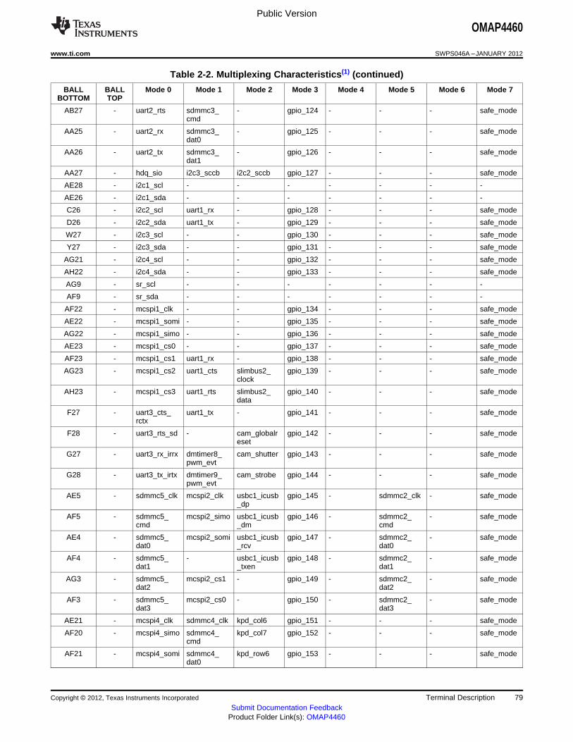
Public Version
OMAP4460
www.ti.com SWPS046A –JANUARY 2012
Table 2-2. Multiplexing Characteristics(1) (continued)
BALL BALL Mode 0 Mode 1 Mode 2 Mode 3 Mode 4 Mode 5 Mode 6 Mode 7BOTTOM TOP
AB27 - uart2_rts sdmmc3_ - gpio_124 - - - safe_modecmd
AA25 - uart2_rx sdmmc3_ - gpio_125 - - - safe_modedat0
AA26 - uart2_tx sdmmc3_ - gpio_126 - - - safe_modedat1
AA27 - hdq_sio i2c3_sccb i2c2_sccb gpio_127 - - - safe_mode
AE28 - i2c1_scl - - - - - - -
AE26 - i2c1_sda - - - - - - -
C26 - i2c2_scl uart1_rx - gpio_128 - - - safe_mode
D26 - i2c2_sda uart1_tx - gpio_129 - - - safe_mode
W27 - i2c3_scl - - gpio_130 - - - safe_mode
Y27 - i2c3_sda - - gpio_131 - - - safe_mode
AG21 - i2c4_scl - - gpio_132 - - - safe_mode
AH22 - i2c4_sda - - gpio_133 - - - safe_mode
AG9 - sr_scl - - - - - - -
AF9 - sr_sda - - - - - - -
AF22 - mcspi1_clk - - gpio_134 - - - safe_mode
AE22 - mcspi1_somi - - gpio_135 - - - safe_mode
AG22 - mcspi1_simo - - gpio_136 - - - safe_mode
AE23 - mcspi1_cs0 - - gpio_137 - - - safe_mode
AF23 - mcspi1_cs1 uart1_rx - gpio_138 - - - safe_mode
AG23 - mcspi1_cs2 uart1_cts slimbus2_ gpio_139 - - - safe_modeclock
AH23 - mcspi1_cs3 uart1_rts slimbus2_ gpio_140 - - - safe_modedata
F27 - uart3_cts_ uart1_tx - gpio_141 - - - safe_moderctx
F28 - uart3_rts_sd - cam_globalr gpio_142 - - - safe_modeeset
G27 - uart3_rx_irrx dmtimer8_ cam_shutter gpio_143 - - - safe_modepwm_evt
G28 - uart3_tx_irtx dmtimer9_ cam_strobe gpio_144 - - - safe_modepwm_evt
AE5 - sdmmc5_clk mcspi2_clk usbc1_icusb gpio_145 - sdmmc2_clk - safe_mode_dp
AF5 - sdmmc5_ mcspi2_simo usbc1_icusb gpio_146 - sdmmc2_ - safe_modecmd _dm cmd
AE4 - sdmmc5_ mcspi2_somi usbc1_icusb gpio_147 - sdmmc2_ - safe_modedat0 _rcv dat0
AF4 - sdmmc5_ - usbc1_icusb gpio_148 - sdmmc2_ - safe_modedat1 _txen dat1
AG3 - sdmmc5_ mcspi2_cs1 - gpio_149 - sdmmc2_ - safe_modedat2 dat2
AF3 - sdmmc5_ mcspi2_cs0 - gpio_150 - sdmmc2_ - safe_modedat3 dat3
AE21 - mcspi4_clk sdmmc4_clk kpd_col6 gpio_151 - - - safe_mode
AF20 - mcspi4_simo sdmmc4_ kpd_col7 gpio_152 - - - safe_modecmd
AF21 - mcspi4_somi sdmmc4_ kpd_row6 gpio_153 - - - safe_modedat0
Copyright © 2012, Texas Instruments Incorporated Terminal Description 79Submit Documentation Feedback
Product Folder Link(s): OMAP4460

Public Version
OMAP4460
SWPS046A –JANUARY 2012 www.ti.com
Table 2-2. Multiplexing Characteristics(1) (continued)
BALL BALL Mode 0 Mode 1 Mode 2 Mode 3 Mode 4 Mode 5 Mode 6 Mode 7BOTTOM TOP
AE20 - mcspi4_cs0 sdmmc4_ kpd_row7 gpio_154 - - - safe_modedat3
AG20 - uart4_rx sdmmc4_ kpd_row8 gpio_155 - - - safe_modedat2
AH19 - uart4_tx sdmmc4_ kpd_col8 gpio_156 - - - safe_modedat1
AG12 - usbb2_ulpitll usbb2_ sdmmc4_ gpio_157 hsi2_cawake - - safe_mode_clk ulpiphy_clk cmd
AF12 - usbb2_ulpitll usbb2_ sdmmc4_clk gpio_158 hsi2_cadata dispc2_ - safe_mode_stp ulpiphy_stp data23
AE12 - usbb2_ulpitll usbb2_ sdmmc4_ gpio_159 hsi2_caflag dispc2_ - safe_mode_dir ulpiphy_dir dat0 data22
AG13 - usbb2_ulpitll usbb2_ sdmmc4_ gpio_160 hsi2_acready dispc2_ - safe_mode_nxt ulpiphy_nxt dat1 data21
AE11 - usbb2_ulpitll usbb2_ sdmmc4_ gpio_161 hsi2_acwake dispc2_ usbb2_mm_ safe_mode_dat0 ulpiphy_dat0 dat2 data20 txen
AF11 - usbb2_ulpitll usbb2_ sdmmc4_ gpio_162 hsi2_acdata dispc2_ usbb2_mm_ safe_mode_dat1 ulpiphy_dat1 dat3 data19 txdat
AG11 - usbb2_ulpitll usbb2_ sdmmc3_ gpio_163 hsi2_acflag dispc2_ usbb2_mm_ safe_mode_dat2 ulpiphy_dat2 dat2 data18 txse0
AH11 - usbb2_ulpitll usbb2_ sdmmc3_ gpio_164 hsi2_caready dispc2_ rfbi_data15 safe_mode_dat3 ulpiphy_dat3 dat1 data15
AE10 - usbb2_ulpitll usbb2_ sdmmc3_ gpio_165 mcspi3_somi dispc2_ rfbi_data14 safe_mode_dat4 ulpiphy_dat4 dat0 data14
AF10 - usbb2_ulpitll usbb2_ sdmmc3_ gpio_166 mcspi3_cs0 dispc2_ rfbi_data13 safe_mode_dat5 ulpiphy_dat5 dat3 data13
AG10 - usbb2_ulpitll usbb2_ sdmmc3_ gpio_167 mcspi3_simo dispc2_ rfbi_data12 safe_mode_dat6 ulpiphy_dat6 cmd data12
AE9 - usbb2_ulpitll usbb2_ sdmmc3_clk gpio_168 mcspi3_clk dispc2_ rfbi_data11 safe_mode_dat7 ulpiphy_dat7 data11
AF13 - usbb2_hsic_ - - gpio_169 - - - safe_modedata
AE13 - usbb2_hsic_ - - gpio_170 - - - safe_modestrobe
G26 - kpd_col3 kpd_col0 cam2_d0(4) gpio_171 - - - safe_mode
G25 - kpd_col4 kpd_col1 cam2_d1(4) gpio_172 - - - safe_mode
H26 - kpd_col5 kpd_col2 cam2_d2(4) gpio_173 - - - safe_mode
H25 - kpd_col0 kpd_col3 cam2_d3(4) gpio_174 - - - safe_mode
J27 - kpd_col1 kpd_col4 cam2_d8(4) gpio_0 - - - safe_mode
H27 - kpd_col2 kpd_col5 cam2_d10(4) gpio_1 - - - safe_mode
J26 - kpd_row3 kpd_row0 cam2_d4(4) gpio_175 - - - safe_mode
J25 - kpd_row4 kpd_row1 cam2_d5(4) gpio_176 - - - safe_mode
K26 - kpd_row5 kpd_row2 cam2_d6(4) gpio_177 - - - safe_mode
K25 - kpd_row0 kpd_row3 cam2_d7(4) gpio_178 - - - safe_mode
L27 - kpd_row1 kpd_row4 cam2_d9(4) gpio_2 - - - safe_mode
K27 - kpd_row2 kpd_row5 cam2_d11(4) gpio_3 - - - safe_mode
C3 - usba0_otg_ - - - - - - -ce
B5 - usba0_otg_ uart3_rx_irrx uart2_rx - - - - safe_modedp
B4 - usba0_otg_ uart3_tx_irtx uart2_tx - - - - safe_modedm
AH6 - fref_xtal_in - - - - - - -
80 Terminal Description Copyright © 2012, Texas Instruments Incorporated
Submit Documentation FeedbackProduct Folder Link(s): OMAP4460

Public Version
OMAP4460
www.ti.com SWPS046A –JANUARY 2012
Table 2-2. Multiplexing Characteristics(1) (continued)
BALL BALL Mode 0 Mode 1 Mode 2 Mode 3 Mode 4 Mode 5 Mode 6 Mode 7BOTTOM TOP
AH5 - fref_xtal_out - - - - - - -
AG5 - fref_xtal_ - - - - - - -vssosc
AG8 - fref_slicer_in - - gpi_wk5 - - - safe_mode
AD1 - fref_clk_ - - - - - - -ioreq
AD2 - fref_clk0_out fref_clk1_req sys_drm_ gpio_wk6 - sdmmc2_ attila_hw_ safe_modemsecure dat7 dbg6
AA28 - fref_clk1_out - - gpio_181 - - - safe_mode
Y28 - fref_clk2_out - - gpio_182 - - - safe_mode
AD3 - fref_clk3_req fref_clk1_req sys_drm_ gpio_ - sdmmc2_ attila_hw_ safe_modemsecure wk30 dat4 dbg7
AD4 - fref_clk3_out fref_clk2_req sys_secure_ gpio_ - sdmmc2_ attila_hw_ safe_modeindicator wk31 dat5 dbg8
AC2 - fref_clk4_req fref_clk5_out - gpio_wk7 - sdmmc2_ attila_hw_ -dat6 dbg9
AC3 - fref_clk4_out - - gpio_wk8 - - attila_hw_ -dbg10
AG7 - sys_32k - - - - - - -
AE7 - sys_ - - - - - - -nrespwron
AF7 - sys_ - - - - - - -nreswarm
AH7 - sys_pwr_req - - - - - - -
AG6 - sys_pwron_ - - gpio_ - attila_hw_ attila_hw_ -reset_out wk29 dbd0 dbg11
AE6 - sys_nirq1 - - - - - - safe_mode
AF6 - sys_nirq2 - - gpio_183 - - - safe_mode
F26 - sys_boot0 - - gpio_184 - - - safe_mode
E27 - sys_boot1 - - gpio_185 - - - safe_mode
E26 - sys_boot2 - - gpio_186 - - - safe_mode
E25 - sys_boot3 - - gpio_187 - - - safe_mode
D28 - sys_boot4 - - gpio_188 - - - safe_mode
D27 - sys_boot5 - - gpio_189 - - - safe_mode
AF8 - sys_boot6 dpm_emu18 - gpio_wk9 - - attila_hw_ safe_modedbg12
AE8 - sys_boot7 dpm_emu19 - gpio_ - - attila_hw_ safe_modewk10 dbg13
AH2 - jtag_ntrst - - - - - - -
AG1 - jtag_tck - - - - - - safe_mode
AE3 - jtag_rtck - - - - - - -
AH1 - jtag_tms_ - - - - - - safe_modetmsc
AE1 - jtag_tdi - - - - - - -
AE2 - jtag_tdo - - - - - - -
M2 - dpm_emu0 - - gpio_11 - - attila_hw_ safe_modedbg0
N2 - dpm_emu1 - - gpio_12 - - attila_hw_ safe_modedbg1
P2 - dpm_emu2 usba0_ - gpio_13 - dispc2_fid attila_hw_ safe_modeulpiphy_clk dbg2
Copyright © 2012, Texas Instruments Incorporated Terminal Description 81Submit Documentation Feedback
Product Folder Link(s): OMAP4460

Public Version
OMAP4460
SWPS046A –JANUARY 2012 www.ti.com
Table 2-2. Multiplexing Characteristics(1) (continued)
BALL BALL Mode 0 Mode 1 Mode 2 Mode 3 Mode 4 Mode 5 Mode 6 Mode 7BOTTOM TOP
V1 - dpm_emu3 usba0_ - gpio_14 rfbi_data10 dispc2_ attila_hw_ safe_modeulpiphy_stp data10 dbg3
V2 - dpm_emu4 usba0_ - gpio_15 rfbi_data9 dispc2_data9 attila_hw_ safe_modeulpiphy_dir dbg4
W1 - dpm_emu5 usba0_ - gpio_16 rfbi_te_ dispc2_ attila_hw_ safe_modeulpiphy_nxt vsync0 data16 dbg5
W2 - dpm_emu6 usba0_ uart3_tx_irtx gpio_17 rfbi_hsync0 dispc2_ attila_hw_ safe_modeulpiphy_dat0 data17 dbg6
W3 - dpm_emu7 usba0_ uart3_rx_irrx gpio_18 rfbi_cs0 dispc2_ attila_hw_ safe_modeulpiphy_dat1 hsync dbg7
W4 - dpm_emu8 usba0_ uart3_rts_sd gpio_19 rfbi_re dispc2_pclk attila_hw_ safe_modeulpiphy_dat2 dbg8
Y2 - dpm_emu9 usba0_ uart3_cts_ gpio_20 rfbi_we dispc2_ attila_hw_ safe_modeulpiphy_dat3 rctx vsync dbg9
Y3 - dpm_emu10 usba0_ - gpio_21 rfbi_a0 dispc2_de attila_hw_ safe_modeulpiphy_dat4 dbg10
Y4 - dpm_emu11 usba0_ - gpio_22 rfbi_data8 dispc2_data8 attila_hw_ safe_modeulpiphy_dat5 dbg11
AA1 - dpm_emu12 usba0_ - gpio_23 rfbi_data7 dispc2_data7 attila_hw_ safe_modeulpiphy_dat6 dbg12
AA2 - dpm_emu13 usba0_ - gpio_24 rfbi_data6 dispc2_data6 attila_hw_ safe_modeulpiphy_dat7 dbg13
AA3 - dpm_emu14 sys_drm_ uart1_rx gpio_25 rfbi_data5 dispc2_data5 attila_hw_ safe_modemsecure dbg14
AA4 - dpm_emu15 sys_secure_ - gpio_26 rfbi_data4 dispc2_data4 attila_hw_ safe_modeindicator dbg15
AB2 - dpm_emu16 dmtimer8_ dsi1_te0 gpio_27 rfbi_data3 dispc2_data3 attila_hw_ safe_modepwm_evt dbg16
AB3 - dpm_emu17 dmtimer9_ dsi1_te1 gpio_28 rfbi_data2 dispc2_data2 attila_hw_ safe_modepwm_evt dbg17
AB4 - dpm_emu18 dmtimer10_ dsi2_te0 gpio_190 rfbi_data1 dispc2_data1 attila_hw_ safe_modepwm_evt dbg18
AC4 - dpm_emu19 dmtimer11_ dsi2_te1 gpio_191 rfbi_data0 dispc2_data0 attila_hw_ safe_modepwm_evt dbg19
82 Terminal Description Copyright © 2012, Texas Instruments Incorporated
Submit Documentation FeedbackProduct Folder Link(s): OMAP4460

Public Version
OMAP4460
www.ti.com SWPS046A –JANUARY 2012
Table 2-2. Multiplexing Characteristics(1) (continued)
BALL BALL Mode 0 Mode 1 Mode 2 Mode 3 Mode 4 Mode 5 Mode 6 Mode 7BOTTOM TOP
H1 / M1 / A2 / A6 / vss - - - - - - -AB1 / C2 / A9 / A11F2 / K2 / / A14 /
U2 / AF2 / A28 / B1B3 / J3 / J4 / B14 // AG4 / B6 / B21 /
K8 / U8 / B24 /AH8 / N9 / B29 /A10 / AH10 E28 / F1
/ H11 / / H28 /AA11 / N12 J1 / L29/ P12 / R12 / M2 / P1/ T12 / U12 / P2 /
/ AA12 / R28 / V2B13 / H13 / / V28 /M13 / N13 / AA28 /P13 / R13 / AB2 /T13 / U13 / AE2 /AH13 / M14 AF28 // N14 / P14 AH1 // R14 / T14 AH5 // U14 / M15 AH14 // N15 / P15 AH18 // R15 / T15 AH29 // U15 / M16 AJ2 // N16 / P16 AJ7 // R16 / T16 AJ11 // U16 / H17 AJ16 // M17 / N17 AJ22 // P17 / R17 AJ28/ T17 / U17
/ Y17 /AG17 / H19
/ A20 /AA20 / J21/ L21 / M21
/ U21 /AH21 / M22/ A23 / F25/ L25 / Y25/ L26 / Y26
/ AG26 /B27 / AE27/ H28 / K28
/ U28
Y22 - vpp(2) - - - - - - -
J8 - vpp_cust(2) - - - - - - -
J9 / K9 / L9 - vdd_core - - - - - - -/ M9 / T9 /J10 / J11 /Y11 / H12 /J12 / Y12 /J13 / Y13 /AA13 / J15/ J16 / J17 /H18 / J18 /J19 / J20 /K20 / L20 /M20 / N20 /R20 / T20 /U20 / V20
V8 / W8 / - vdd_mpu - - - - - - -Y8 / U9 /V9 / W9 /Y9 / Y10 /
AA10
Copyright © 2012, Texas Instruments Incorporated Terminal Description 83Submit Documentation Feedback
Product Folder Link(s): OMAP4460
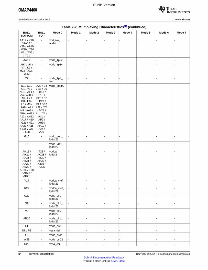
Public Version
OMAP4460
SWPS046A –JANUARY 2012 www.ti.com
Table 2-2. Multiplexing Characteristics(1) (continued)
BALL BALL Mode 0 Mode 1 Mode 2 Mode 3 Mode 4 Mode 5 Mode 6 Mode 7BOTTOM TOP
AA17 / Y18 - vdd_iva_ - - - - - - -/ AA18 / audio
Y19 / AA19/ W20 / Y20/ V21 / W21
/ Y21
AA16 - vdds_1p2v - - - - - - -
AB7 / U7 / - vdds_1p8v - - - - - - -V7 / K7 /
H22 / J22 /W22
Y7 - vdds_1p8_ - - - - - - -fref
D1 / G1 / A22 / B4 vddq_lpddr2 - - - - - - -U1 / Y1 / / B7 / B9
AC1 / AF1 / / B13 /A4 / AH4 / B18 /A6 / L7 / B25 / D2G8 / H8 / / D29 /L8 / M8 / F29 / G2
AA8 / A9 / / J2 / J28H9 / AA9 / / M28 /
AB9 / AH9 / U1 / Y1 /A12 / AH12 AC1 // A17 / H20 AF2 // G21 / H21 AH9 // A22 / A25 AH12 // E28 / J28 AJ4 /
/ L28 AJ6
G15 - vddq_vref_ - - - - - - -lpddr21
T8 - vddq_vref_ - - - - - - -lpddr22
AH18 / T28 / vddca_ - - - - - - -AH20 / AC28 / lpddr2AA21 / AE29 /AB21 / AH22 /AA22 / AJ19 /AB22 / AJ26
AH25 / T28/ AB28 /AD28
Y14 - vddca_vref_ - - - - - - -lpddr21
R27 - vddca_vref_ - - - - - - -lpddr22
G22 - vdda_dll0_ - - - - - - -lpddr21
G9 - vdda_dll1_ - - - - - - -lpddr21
M7 - vdda_dll0_ - - - - - - -lpddr22
AB10 - vdda_dll1_ - - - - - - -lpddr22
L1 - vdda_dsi1 - - - - - - -
N8 / P8 - vssa_dsi - - - - - - -
L2 - vdda_dsi2 - - - - - - -
W28 - vdda_csi21 - - - - - - -
R22 - vssa_csi2 - - - - - - -
84 Terminal Description Copyright © 2012, Texas Instruments Incorporated
Submit Documentation FeedbackProduct Folder Link(s): OMAP4460

Public Version
OMAP4460
www.ti.com SWPS046A –JANUARY 2012
Table 2-2. Multiplexing Characteristics(1) (continued)
BALL BALL Mode 0 Mode 1 Mode 2 Mode 3 Mode 4 Mode 5 Mode 6 Mode 7BOTTOM TOP
V28 - vdda_csi22 - - - - - - -
A11 / G12 - vdda_hdmi_ - - - - - - -vdac
G11 - vssa_hdmi_ - - - - - - -vdac
A5 - vdda_ - - - - - - -usba0otg_3p3v
G10 - vssa_ - - - - - - -usba0otg_3p3v
A7 - vdda_ - - - - - - -usba0otg_1p8v
H10 - vssa_ - - - - - - -usba0otg
J7 - vdds_usim - - - - - - -
A2 - pbias_sim - - - - - - -
G7 / H7 - vdds_ - - - - - - -sdmmc1
A1 - pbias_mmc1 - - - - - - -
P9 - vdda_dpll_ - - - - - - -mpu
G13 - vdda_dpll_ - - - - - - -core_audio
Y16 - vdda_dpll_ - - - - - - -iva_per
G20 - vdds_dv_ - - - - - - -gpmc
G16 / H16 - vdds_dv_ - - - - - - -sdmmc2
G17 / G18 / - vdds_dv_c2c - - - - - - -G19
V22 - vdds_dv_ - - - - - - -cam
AB16 - vdds_dv_ - - - - - - -bank0
AB20 - vdds_dv_ - - - - - - -bank1
AB8 / AB19 - vdds_dv_ - - - - - - -bank2
AB18 - vdds_dv_ - - - - - - -bank3
AA7 - vdds_dv_ - - - - - - -bank4
AB17 - vdds_dv_ - - - - - - -bank5
AA14 - vdds_dv_ - - - - - - -bank6
M28 - vdds_dv_ - - - - - - -bank7
W7 - vdds_dv_fref - - - - - - -
AB14 - vdda_ldo_ - - - - - - -sram_mpu
Copyright © 2012, Texas Instruments Incorporated Terminal Description 85Submit Documentation Feedback
Product Folder Link(s): OMAP4460
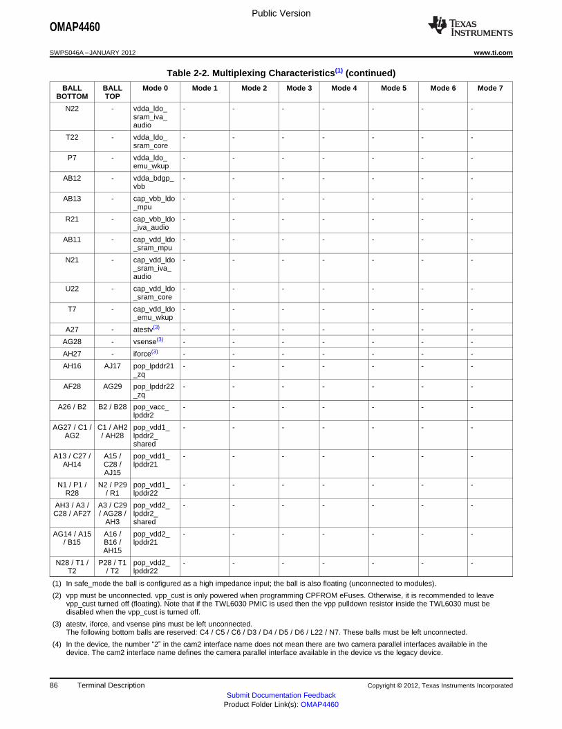
Public Version
OMAP4460
SWPS046A –JANUARY 2012 www.ti.com
Table 2-2. Multiplexing Characteristics(1) (continued)
BALL BALL Mode 0 Mode 1 Mode 2 Mode 3 Mode 4 Mode 5 Mode 6 Mode 7BOTTOM TOP
N22 - vdda_ldo_ - - - - - - -sram_iva_audio
T22 - vdda_ldo_ - - - - - - -sram_core
P7 - vdda_ldo_ - - - - - - -emu_wkup
AB12 - vdda_bdgp_ - - - - - - -vbb
AB13 - cap_vbb_ldo - - - - - - -_mpu
R21 - cap_vbb_ldo - - - - - - -_iva_audio
AB11 - cap_vdd_ldo - - - - - - -_sram_mpu
N21 - cap_vdd_ldo - - - - - - -_sram_iva_audio
U22 - cap_vdd_ldo - - - - - - -_sram_core
T7 - cap_vdd_ldo - - - - - - -_emu_wkup
A27 - atestv(3) - - - - - - -
AG28 - vsense(3) - - - - - - -
AH27 - iforce(3) - - - - - - -
AH16 AJ17 pop_lpddr21 - - - - - - -_zq
AF28 AG29 pop_lpddr22 - - - - - - -_zq
A26 / B2 B2 / B28 pop_vacc_ - - - - - - -lpddr2
AG27 / C1 / C1 / AH2 pop_vdd1_ - - - - - - -AG2 / AH28 lpddr2_
shared
A13 / C27 / A15 / pop_vdd1_ - - - - - - -AH14 C28 / lpddr21
AJ15
N1 / P1 / N2 / P29 pop_vdd1_ - - - - - - -R28 / R1 lpddr22
AH3 / A3 / A3 / C29 pop_vdd2_ - - - - - - -C28 / AF27 / AG28 / lpddr2_
AH3 shared
AG14 / A15 A16 / pop_vdd2_ - - - - - - -/ B15 B16 / lpddr21
AH15
N28 / T1 / P28 / T1 pop_vdd2_ - - - - - - -T2 / T2 lpddr22
(1) In safe_mode the ball is configured as a high impedance input; the ball is also floating (unconnected to modules).
(2) vpp must be unconnected. vpp_cust is only powered when programming CPFROM eFuses. Otherwise, it is recommended to leavevpp_cust turned off (floating). Note that if the TWL6030 PMIC is used then the vpp pulldown resistor inside the TWL6030 must bedisabled when the vpp_cust is turned off.
(3) atestv, iforce, and vsense pins must be left unconnected.The following bottom balls are reserved: C4 / C5 / C6 / D3 / D4 / D5 / D6 / L22 / N7. These balls must be left unconnected.
(4) In the device, the number “2” in the cam2 interface name does not mean there are two camera parallel interfaces available in thedevice. The cam2 interface name defines the camera parallel interface available in the device vs the legacy device.
86 Terminal Description Copyright © 2012, Texas Instruments Incorporated
Submit Documentation FeedbackProduct Folder Link(s): OMAP4460
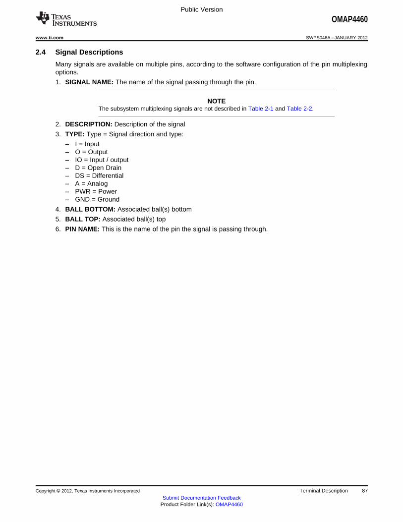
Public Version
OMAP4460
www.ti.com SWPS046A –JANUARY 2012
2.4 Signal Descriptions
Many signals are available on multiple pins, according to the software configuration of the pin multiplexingoptions.
1. SIGNAL NAME: The name of the signal passing through the pin.
NOTEThe subsystem multiplexing signals are not described in Table 2-1 and Table 2-2.
2. DESCRIPTION: Description of the signal
3. TYPE: Type = Signal direction and type:
– I = Input– O = Output– IO = Input / output– D = Open Drain– DS = Differential– A = Analog– PWR = Power– GND = Ground
4. BALL BOTTOM: Associated ball(s) bottom
5. BALL TOP: Associated ball(s) top
6. PIN NAME: This is the name of the pin the signal is passing through.
Copyright © 2012, Texas Instruments Incorporated Terminal Description 87Submit Documentation Feedback
Product Folder Link(s): OMAP4460
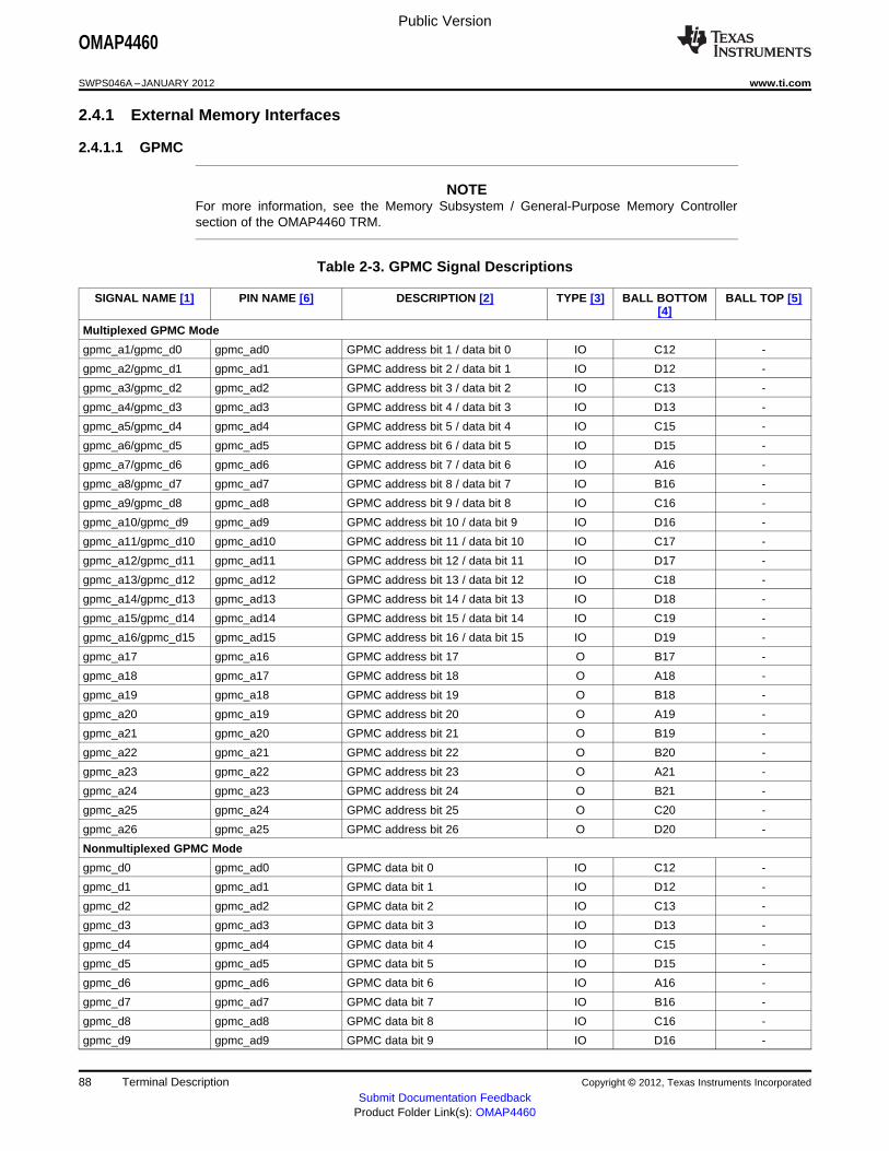
Public Version
OMAP4460
SWPS046A –JANUARY 2012 www.ti.com
2.4.1 External Memory Interfaces
2.4.1.1 GPMC
NOTEFor more information, see the Memory Subsystem / General-Purpose Memory Controllersection of the OMAP4460 TRM.
Table 2-3. GPMC Signal Descriptions
SIGNAL NAME [1] PIN NAME [6] DESCRIPTION [2] TYPE [3] BALL BOTTOM BALL TOP [5][4]
Multiplexed GPMC Mode
gpmc_a1/gpmc_d0 gpmc_ad0 GPMC address bit 1 / data bit 0 IO C12 -
gpmc_a2/gpmc_d1 gpmc_ad1 GPMC address bit 2 / data bit 1 IO D12 -
gpmc_a3/gpmc_d2 gpmc_ad2 GPMC address bit 3 / data bit 2 IO C13 -
gpmc_a4/gpmc_d3 gpmc_ad3 GPMC address bit 4 / data bit 3 IO D13 -
gpmc_a5/gpmc_d4 gpmc_ad4 GPMC address bit 5 / data bit 4 IO C15 -
gpmc_a6/gpmc_d5 gpmc_ad5 GPMC address bit 6 / data bit 5 IO D15 -
gpmc_a7/gpmc_d6 gpmc_ad6 GPMC address bit 7 / data bit 6 IO A16 -
gpmc_a8/gpmc_d7 gpmc_ad7 GPMC address bit 8 / data bit 7 IO B16 -
gpmc_a9/gpmc_d8 gpmc_ad8 GPMC address bit 9 / data bit 8 IO C16 -
gpmc_a10/gpmc_d9 gpmc_ad9 GPMC address bit 10 / data bit 9 IO D16 -
gpmc_a11/gpmc_d10 gpmc_ad10 GPMC address bit 11 / data bit 10 IO C17 -
gpmc_a12/gpmc_d11 gpmc_ad11 GPMC address bit 12 / data bit 11 IO D17 -
gpmc_a13/gpmc_d12 gpmc_ad12 GPMC address bit 13 / data bit 12 IO C18 -
gpmc_a14/gpmc_d13 gpmc_ad13 GPMC address bit 14 / data bit 13 IO D18 -
gpmc_a15/gpmc_d14 gpmc_ad14 GPMC address bit 15 / data bit 14 IO C19 -
gpmc_a16/gpmc_d15 gpmc_ad15 GPMC address bit 16 / data bit 15 IO D19 -
gpmc_a17 gpmc_a16 GPMC address bit 17 O B17 -
gpmc_a18 gpmc_a17 GPMC address bit 18 O A18 -
gpmc_a19 gpmc_a18 GPMC address bit 19 O B18 -
gpmc_a20 gpmc_a19 GPMC address bit 20 O A19 -
gpmc_a21 gpmc_a20 GPMC address bit 21 O B19 -
gpmc_a22 gpmc_a21 GPMC address bit 22 O B20 -
gpmc_a23 gpmc_a22 GPMC address bit 23 O A21 -
gpmc_a24 gpmc_a23 GPMC address bit 24 O B21 -
gpmc_a25 gpmc_a24 GPMC address bit 25 O C20 -
gpmc_a26 gpmc_a25 GPMC address bit 26 O D20 -
Nonmultiplexed GPMC Mode
gpmc_d0 gpmc_ad0 GPMC data bit 0 IO C12 -
gpmc_d1 gpmc_ad1 GPMC data bit 1 IO D12 -
gpmc_d2 gpmc_ad2 GPMC data bit 2 IO C13 -
gpmc_d3 gpmc_ad3 GPMC data bit 3 IO D13 -
gpmc_d4 gpmc_ad4 GPMC data bit 4 IO C15 -
gpmc_d5 gpmc_ad5 GPMC data bit 5 IO D15 -
gpmc_d6 gpmc_ad6 GPMC data bit 6 IO A16 -
gpmc_d7 gpmc_ad7 GPMC data bit 7 IO B16 -
gpmc_d8 gpmc_ad8 GPMC data bit 8 IO C16 -
gpmc_d9 gpmc_ad9 GPMC data bit 9 IO D16 -
88 Terminal Description Copyright © 2012, Texas Instruments Incorporated
Submit Documentation FeedbackProduct Folder Link(s): OMAP4460
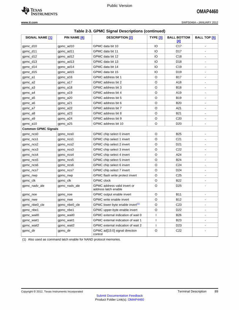
Public Version
OMAP4460
www.ti.com SWPS046A –JANUARY 2012
Table 2-3. GPMC Signal Descriptions (continued)
SIGNAL NAME [1] PIN NAME [6] DESCRIPTION [2] TYPE [3] BALL BOTTOM BALL TOP [5][4]
gpmc_d10 gpmc_ad10 GPMC data bit 10 IO C17 -
gpmc_d11 gpmc_ad11 GPMC data bit 11 IO D17 -
gpmc_d12 gpmc_ad12 GPMC data bit 12 IO C18 -
gpmc_d13 gpmc_ad13 GPMC data bit 13 IO D18 -
gpmc_d14 gpmc_ad14 GPMC data bit 14 IO C19 -
gpmc_d15 gpmc_ad15 GPMC data bit 15 IO D19 -
gpmc_a1 gpmc_a16 GPMC address bit 1 O B17 -
gpmc_a2 gpmc_a17 GPMC address bit 2 O A18 -
gpmc_a3 gpmc_a18 GPMC address bit 3 O B18 -
gpmc_a4 gpmc_a19 GPMC address bit 4 O A19 -
gpmc_a5 gpmc_a20 GPMC address bit 5 O B19 -
gpmc_a6 gpmc_a21 GPMC address bit 6 O B20 -
gpmc_a7 gpmc_a22 GPMC address bit 7 O A21 -
gpmc_a8 gpmc_a23 GPMC address bit 8 O B21 -
gpmc_a9 gpmc_a24 GPMC address bit 9 O C20 -
gpmc_a10 gpmc_a25 GPMC address bit 10 O D20 -
Common GPMC Signals
gpmc_ncs0 gpmc_ncs0 GPMC chip select 0 invert O B25 -
gpmc_ncs1 gpmc_ncs1 GPMC chip select 1 invert O C21 -
gpmc_ncs2 gpmc_ncs2 GPMC chip select 2 invert O D21 -
gpmc_ncs3 gpmc_ncs3 GPMC chip select 3 invert O C22 -
gpmc_ncs4 gpmc_ncs4 GPMC chip select 4 invert O A24 -
gpmc_ncs5 gpmc_ncs5 GPMC chip select 5 invert O B24 -
gpmc_ncs6 gpmc_ncs6 GPMC chip select 6 invert O C24 -
gpmc_ncs7 gpmc_ncs7 GPMC chip select 7 invert O D24 -
gpmc_nwp gpmc_nwp GPMC flash write protect invert O C25 -
gpmc_clk gpmc_clk GPMC clock O B22 -
gpmc_nadv_ale gpmc_nadv_ale GPMC address valid invert or O D25 -address latch enable
gpmc_noe gpmc_noe GPMC output enable invert O B11 -
gpmc_nwe gpmc_nwe GPMC write enable invert O B12 -
gpmc_nbe0_cle gpmc_nbe0_cle GPMC lower-byte enable invert(1) O C23 -
gpmc_nbe1 gpmc_nbe1 GPMC upper-byte enable invert O D22 -
gpmc_wait0 gpmc_wait0 GPMC external indication of wait 0 I B26 -
gpmc_wait1 gpmc_wait1 GPMC external indication of wait 1 I B23 -
gpmc_wait2 gpmc_wait2 GPMC external indication of wait 2 I D23 -
gpmc_dir gpmc_dir GPMC ad[15:0] signal direction O C22 -control
(1) Also used as command latch enable for NAND protocol memories.
Copyright © 2012, Texas Instruments Incorporated Terminal Description 89Submit Documentation Feedback
Product Folder Link(s): OMAP4460
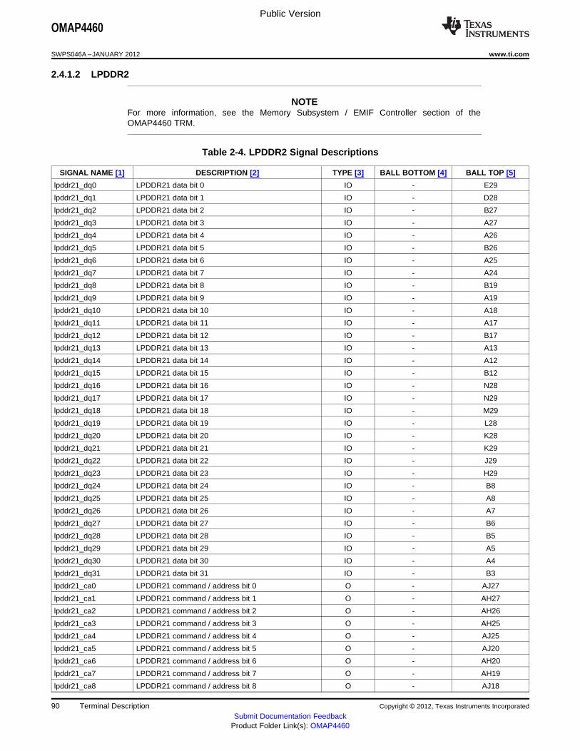
Public Version
OMAP4460
SWPS046A –JANUARY 2012 www.ti.com
2.4.1.2 LPDDR2
NOTEFor more information, see the Memory Subsystem / EMIF Controller section of theOMAP4460 TRM.
Table 2-4. LPDDR2 Signal Descriptions
SIGNAL NAME [1] DESCRIPTION [2] TYPE [3] BALL BOTTOM [4] BALL TOP [5]
lpddr21_dq0 LPDDR21 data bit 0 IO - E29
lpddr21_dq1 LPDDR21 data bit 1 IO - D28
lpddr21_dq2 LPDDR21 data bit 2 IO - B27
lpddr21_dq3 LPDDR21 data bit 3 IO - A27
lpddr21_dq4 LPDDR21 data bit 4 IO - A26
lpddr21_dq5 LPDDR21 data bit 5 IO - B26
lpddr21_dq6 LPDDR21 data bit 6 IO - A25
lpddr21_dq7 LPDDR21 data bit 7 IO - A24
lpddr21_dq8 LPDDR21 data bit 8 IO - B19
lpddr21_dq9 LPDDR21 data bit 9 IO - A19
lpddr21_dq10 LPDDR21 data bit 10 IO - A18
lpddr21_dq11 LPDDR21 data bit 11 IO - A17
lpddr21_dq12 LPDDR21 data bit 12 IO - B17
lpddr21_dq13 LPDDR21 data bit 13 IO - A13
lpddr21_dq14 LPDDR21 data bit 14 IO - A12
lpddr21_dq15 LPDDR21 data bit 15 IO - B12
lpddr21_dq16 LPDDR21 data bit 16 IO - N28
lpddr21_dq17 LPDDR21 data bit 17 IO - N29
lpddr21_dq18 LPDDR21 data bit 18 IO - M29
lpddr21_dq19 LPDDR21 data bit 19 IO - L28
lpddr21_dq20 LPDDR21 data bit 20 IO - K28
lpddr21_dq21 LPDDR21 data bit 21 IO - K29
lpddr21_dq22 LPDDR21 data bit 22 IO - J29
lpddr21_dq23 LPDDR21 data bit 23 IO - H29
lpddr21_dq24 LPDDR21 data bit 24 IO - B8
lpddr21_dq25 LPDDR21 data bit 25 IO - A8
lpddr21_dq26 LPDDR21 data bit 26 IO - A7
lpddr21_dq27 LPDDR21 data bit 27 IO - B6
lpddr21_dq28 LPDDR21 data bit 28 IO - B5
lpddr21_dq29 LPDDR21 data bit 29 IO - A5
lpddr21_dq30 LPDDR21 data bit 30 IO - A4
lpddr21_dq31 LPDDR21 data bit 31 IO - B3
lpddr21_ca0 LPDDR21 command / address bit 0 O - AJ27
lpddr21_ca1 LPDDR21 command / address bit 1 O - AH27
lpddr21_ca2 LPDDR21 command / address bit 2 O - AH26
lpddr21_ca3 LPDDR21 command / address bit 3 O - AH25
lpddr21_ca4 LPDDR21 command / address bit 4 O - AJ25
lpddr21_ca5 LPDDR21 command / address bit 5 O - AJ20
lpddr21_ca6 LPDDR21 command / address bit 6 O - AH20
lpddr21_ca7 LPDDR21 command / address bit 7 O - AH19
lpddr21_ca8 LPDDR21 command / address bit 8 O - AJ18
90 Terminal Description Copyright © 2012, Texas Instruments Incorporated
Submit Documentation FeedbackProduct Folder Link(s): OMAP4460
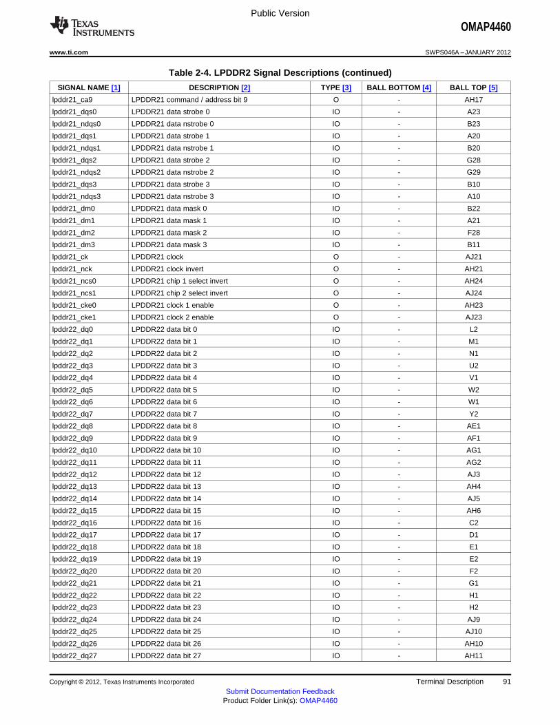
Public Version
OMAP4460
www.ti.com SWPS046A –JANUARY 2012
Table 2-4. LPDDR2 Signal Descriptions (continued)
SIGNAL NAME [1] DESCRIPTION [2] TYPE [3] BALL BOTTOM [4] BALL TOP [5]
lpddr21_ca9 LPDDR21 command / address bit 9 O - AH17
lpddr21_dqs0 LPDDR21 data strobe 0 IO - A23
lpddr21_ndqs0 LPDDR21 data nstrobe 0 IO - B23
lpddr21_dqs1 LPDDR21 data strobe 1 IO - A20
lpddr21_ndqs1 LPDDR21 data nstrobe 1 IO - B20
lpddr21_dqs2 LPDDR21 data strobe 2 IO - G28
lpddr21_ndqs2 LPDDR21 data nstrobe 2 IO - G29
lpddr21_dqs3 LPDDR21 data strobe 3 IO - B10
lpddr21_ndqs3 LPDDR21 data nstrobe 3 IO - A10
lpddr21_dm0 LPDDR21 data mask 0 IO - B22
lpddr21_dm1 LPDDR21 data mask 1 IO - A21
lpddr21_dm2 LPDDR21 data mask 2 IO - F28
lpddr21_dm3 LPDDR21 data mask 3 IO - B11
lpddr21_ck LPDDR21 clock O - AJ21
lpddr21_nck LPDDR21 clock invert O - AH21
lpddr21_ncs0 LPDDR21 chip 1 select invert O - AH24
lpddr21_ncs1 LPDDR21 chip 2 select invert O - AJ24
lpddr21_cke0 LPDDR21 clock 1 enable O - AH23
lpddr21_cke1 LPDDR21 clock 2 enable O - AJ23
lpddr22_dq0 LPDDR22 data bit 0 IO - L2
lpddr22_dq1 LPDDR22 data bit 1 IO - M1
lpddr22_dq2 LPDDR22 data bit 2 IO - N1
lpddr22_dq3 LPDDR22 data bit 3 IO - U2
lpddr22_dq4 LPDDR22 data bit 4 IO - V1
lpddr22_dq5 LPDDR22 data bit 5 IO - W2
lpddr22_dq6 LPDDR22 data bit 6 IO - W1
lpddr22_dq7 LPDDR22 data bit 7 IO - Y2
lpddr22_dq8 LPDDR22 data bit 8 IO - AE1
lpddr22_dq9 LPDDR22 data bit 9 IO - AF1
lpddr22_dq10 LPDDR22 data bit 10 IO - AG1
lpddr22_dq11 LPDDR22 data bit 11 IO - AG2
lpddr22_dq12 LPDDR22 data bit 12 IO - AJ3
lpddr22_dq13 LPDDR22 data bit 13 IO - AH4
lpddr22_dq14 LPDDR22 data bit 14 IO - AJ5
lpddr22_dq15 LPDDR22 data bit 15 IO - AH6
lpddr22_dq16 LPDDR22 data bit 16 IO - C2
lpddr22_dq17 LPDDR22 data bit 17 IO - D1
lpddr22_dq18 LPDDR22 data bit 18 IO - E1
lpddr22_dq19 LPDDR22 data bit 19 IO - E2
lpddr22_dq20 LPDDR22 data bit 20 IO - F2
lpddr22_dq21 LPDDR22 data bit 21 IO - G1
lpddr22_dq22 LPDDR22 data bit 22 IO - H1
lpddr22_dq23 LPDDR22 data bit 23 IO - H2
lpddr22_dq24 LPDDR22 data bit 24 IO - AJ9
lpddr22_dq25 LPDDR22 data bit 25 IO - AJ10
lpddr22_dq26 LPDDR22 data bit 26 IO - AH10
lpddr22_dq27 LPDDR22 data bit 27 IO - AH11
Copyright © 2012, Texas Instruments Incorporated Terminal Description 91Submit Documentation Feedback
Product Folder Link(s): OMAP4460
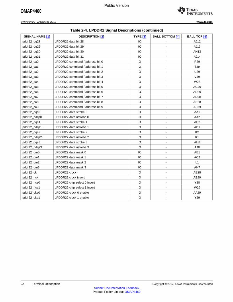
Public Version
OMAP4460
SWPS046A –JANUARY 2012 www.ti.com
Table 2-4. LPDDR2 Signal Descriptions (continued)
SIGNAL NAME [1] DESCRIPTION [2] TYPE [3] BALL BOTTOM [4] BALL TOP [5]
lpddr22_dq28 LPDDR22 data bit 28 IO - AJ12
lpddr22_dq29 LPDDR22 data bit 29 IO - AJ13
lpddr22_dq30 LPDDR22 data bit 30 IO - AH13
lpddr22_dq31 LPDDR22 data bit 31 IO - AJ14
lpddr22_ca0 LPDDR22 command / address bit 0 O - R29
lpddr22_ca1 LPDDR22 command / address bit 1 O - T29
lpddr22_ca2 LPDDR22 command / address bit 2 O - U29
lpddr22_ca3 LPDDR22 command / address bit 3 O - V29
lpddr22_ca4 LPDDR22 command / address bit 4 O - W28
lpddr22_ca5 LPDDR22 command / address bit 5 O - AC29
lpddr22_ca6 LPDDR22 command / address bit 6 O - AD29
lpddr22_ca7 LPDDR22 command / address bit 7 O - AD28
lpddr22_ca8 LPDDR22 command / address bit 8 O - AE28
lpddr22_ca9 LPDDR22 command / address bit 9 O - AF29
lpddr22_dqs0 LPDDR22 data strobe 0 O - AA1
lpddr22_ndqs0 LPDDR22 data nstrobe 0 O - AA2
lpddr22_dqs1 LPDDR22 data strobe 1 O - AD2
lpddr22_ndqs1 LPDDR22 data nstrobe 1 O - AD1
lpddr22_dqs2 LPDDR22 data strobe 2 O - K2
lpddr22_ndqs2 LPDDR22 data nstrobe 2 O - K1
lpddr22_dqs3 LPDDR22 data strobe 3 O - AH8
lpddr22_ndqs3 LPDDR22 data nstrobe 3 O - AJ8
lpddr22_dm0 LPDDR22 data mask 0 IO - AB1
lpddr22_dm1 LPDDR22 data mask 1 IO - AC2
lpddr22_dm2 LPDDR22 data mask 2 IO - L1
lpddr22_dm3 LPDDR22 data mask 3 IO - AH7
lpddr22_ck LPDDR22 clock O - AB28
lpddr22_nck LPDDR22 clock invert O - AB29
lpddr22_ncs0 LPDDR22 chip select 0 invert O - Y28
lpddr22_ncs1 LPDDR22 chip select 1 invert O - W29
lpddr22_cke0 LPDDR22 clock 0 enable O - AA29
lpddr22_cke1 LPDDR22 clock 1 enable O - Y29
92 Terminal Description Copyright © 2012, Texas Instruments Incorporated
Submit Documentation FeedbackProduct Folder Link(s): OMAP4460
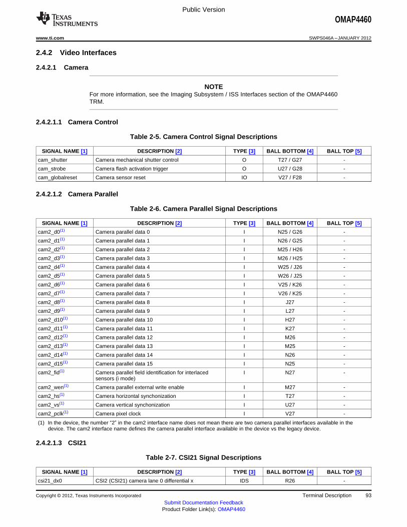
Public Version
OMAP4460
www.ti.com SWPS046A –JANUARY 2012
2.4.2 Video Interfaces
2.4.2.1 Camera
NOTEFor more information, see the Imaging Subsystem / ISS Interfaces section of the OMAP4460TRM.
2.4.2.1.1 Camera Control
Table 2-5. Camera Control Signal Descriptions
SIGNAL NAME [1] DESCRIPTION [2] TYPE [3] BALL BOTTOM [4] BALL TOP [5]
cam_shutter Camera mechanical shutter control O T27 / G27 -
cam_strobe Camera flash activation trigger O U27 / G28 -
cam_globalreset Camera sensor reset IO V27 / F28 -
2.4.2.1.2 Camera Parallel
Table 2-6. Camera Parallel Signal Descriptions
SIGNAL NAME [1] DESCRIPTION [2] TYPE [3] BALL BOTTOM [4] BALL TOP [5]
cam2_d0(1) Camera parallel data 0 I N25 / G26 -
cam2_d1(1) Camera parallel data 1 I N26 / G25 -
cam2_d2(1) Camera parallel data 2 I M25 / H26 -
cam2_d3(1) Camera parallel data 3 I M26 / H25 -
cam2_d4(1) Camera parallel data 4 I W25 / J26 -
cam2_d5(1) Camera parallel data 5 I W26 / J25 -
cam2_d6(1) Camera parallel data 6 I V25 / K26 -
cam2_d7(1) Camera parallel data 7 I V26 / K25 -
cam2_d8(1) Camera parallel data 8 I J27 -
cam2_d9(1) Camera parallel data 9 I L27 -
cam2_d10(1) Camera parallel data 10 I H27 -
cam2_d11(1) Camera parallel data 11 I K27 -
cam2_d12(1) Camera parallel data 12 I M26 -
cam2_d13(1) Camera parallel data 13 I M25 -
cam2_d14(1) Camera parallel data 14 I N26 -
cam2_d15(1) Camera parallel data 15 I N25 -
cam2_fid(1) Camera parallel field identification for interlaced I N27 -sensors (i mode)
cam2_wen(1) Camera parallel external write enable I M27 -
cam2_hs(1) Camera horizontal synchonization I T27 -
cam2_vs(1) Camera vertical synchonization I U27 -
cam2_pclk(1) Camera pixel clock I V27 -
(1) In the device, the number “2” in the cam2 interface name does not mean there are two camera parallel interfaces available in thedevice. The cam2 interface name defines the camera parallel interface available in the device vs the legacy device.
2.4.2.1.3 CSI21
Table 2-7. CSI21 Signal Descriptions
SIGNAL NAME [1] DESCRIPTION [2] TYPE [3] BALL BOTTOM [4] BALL TOP [5]
csi21_dx0 CSI2 (CSI21) camera lane 0 differential x IDS R26 -
Copyright © 2012, Texas Instruments Incorporated Terminal Description 93Submit Documentation Feedback
Product Folder Link(s): OMAP4460
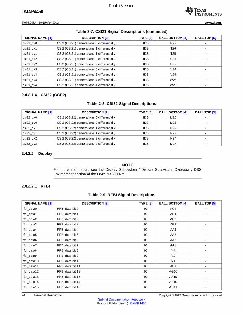
Public Version
OMAP4460
SWPS046A –JANUARY 2012 www.ti.com
Table 2-7. CSI21 Signal Descriptions (continued)
SIGNAL NAME [1] DESCRIPTION [2] TYPE [3] BALL BOTTOM [4] BALL TOP [5]
csi21_dy0 CSI2 (CSI21) camera lane 0 differential y IDS R25 -
csi21_dx1 CSI2 (CSI21) camera lane 1 differential x IDS T26 -
csi21_dy1 CSI2 (CSI21) camera lane 1 differential y IDS T25 -
csi21_dx2 CSI2 (CSI21) camera lane 2 differential x IDS U26 -
csi21_dy2 CSI2 (CSI21) camera lane 2 differential y IDS U25 -
csi21_dx3 CSI2 (CSI21) camera lane 3 differential x IDS V26 -
csi21_dy3 CSI2 (CSI21) camera lane 3 differential y IDS V25 -
csi21_dx4 CSI2 (CSI21) camera lane 4 differential x IDS W26 -
csi21_dy4 CSI2 (CSI21) camera lane 4 differential y IDS W25 -
2.4.2.1.4 CSI22 (CCP2)
Table 2-8. CSI22 Signal Descriptions
SIGNAL NAME [1] DESCRIPTION [2] TYPE [3] BALL BOTTOM [4] BALL TOP [5]
csi22_dx0 CSI2 (CSI22) camera lane 0 differential x IDS M26 -
csi22_dy0 CSI2 (CSI22) camera lane 0 differential y IDS M25 -
csi22_dx1 CSI2 (CSI22) camera lane 1 differential x IDS N26 -
csi22_dy1 CSI2 (CSI22) camera lane 1 differential y IDS N25 -
csi22_dx2 CSI2 (CSI22) camera lane 2 differential x IDS N27 -
csi22_dy2 CSI2 (CSI22) camera lane 2 differential y IDS M27 -
2.4.2.2 Display
NOTEFor more information, see the Display Subsystem / Display Subsystem Overview / DSSEnvironment section of the OMAP4460 TRM.
2.4.2.2.1 RFBI
Table 2-9. RFBI Signal Descriptions
SIGNAL NAME [1] DESCRIPTION [2] TYPE [3] BALL BOTTOM [4] BALL TOP [5]
rfbi_data0 RFBI data bit 0 IO AC4 -
rfbi_data1 RFBI data bit 1 IO AB4 -
rfbi_data2 RFBI data bit 2 IO AB3 -
rfbi_data3 RFBI data bit 3 IO AB2 -
rfbi_data4 RFBI data bit 4 IO AA4 -
rfbi_data5 RFBI data bit 5 IO AA3 -
rfbi_data6 RFBI data bit 6 IO AA2 -
rfbi_data7 RFBI data bit 7 IO AA1 -
rfbi_data8 RFBI data bit 8 IO Y4 -
rfbi_data9 RFBI data bit 9 IO V2 -
rfbi_data10 RFBI data bit 10 IO V1 -
rfbi_data11 RFBI data bit 11 IO AE9 -
rfbi_data12 RFBI data bit 12 IO AG10 -
rfbi_data13 RFBI data bit 13 IO AF10 -
rfbi_data14 RFBI data bit 14 IO AE10 -
rfbi_data15 RFBI data bit 15 IO AH11 -
94 Terminal Description Copyright © 2012, Texas Instruments Incorporated
Submit Documentation FeedbackProduct Folder Link(s): OMAP4460

Public Version
OMAP4460
www.ti.com SWPS046A –JANUARY 2012
Table 2-9. RFBI Signal Descriptions (continued)
SIGNAL NAME [1] DESCRIPTION [2] TYPE [3] BALL BOTTOM [4] BALL TOP [5]
rfbi_a0 RFBI data / control selection O Y3 -
rfbi_we RFBI write enable O Y2 -
rfbi_re RFBI read enable O W4 -
rfbi_cs0 RFBI chip select O W3 -
rfbi_te_vsync0 RFBI vertical synchronization / tearing effect control I W1 -signal
rfbi_hsync0 RFBI horizontal synchronization / tearing effect I W2 -control signal
2.4.2.2.2 DSI1
Table 2-10. DSI1 Signal Descriptions
SIGNAL NAME [1] DESCRIPTION [2] TYPE [3] BALL BOTTOM [4] BALL TOP [5]
dsi1_dx0 DSI1 display lane 0 differential positive or negative IODS P3 -
dsi1_dy0 DSI1 display lane 0 differential positive or negative IODS P4 -
dsi1_dx1 DSI1 display lane 1 differential positive or negative IODS N3 -
dsi1_dy1 DSI1 display lane 1 differential positive or negative IODS N4 -
dsi1_dx2 DSI1 display lane 2 differential positive or negative IODS M3 -
dsi1_dy2 DSI1 display lane 2 differential positive or negative IODS M4 -
dsi1_dx3 DSI1 display lane 3 differential positive or negative IODS L3 -
dsi1_dy3 DSI1 display lane 3 differential positive or negative IODS L4 -
dsi1_dx4 DSI1 display lane 4 differential positive or negative IODS K3 -
dsi1_dy4 DSI1 display lane 4 differential positive or negative IODS K4 -
dsi1_te0 DSI1 tearing effect input 0 IDS C25 / A24 / AB2 -
dsi1_te1 DSI1 tearing effect input 1 IDS D25 / B24 / AB3 -
2.4.2.2.3 DSI2
Table 2-11. DSI2 Signal Descriptions
SIGNAL NAME [1] DESCRIPTION [2] TYPE [3] BALL BOTTOM [4] BALL TOP [5]
dsi2_dx0 DSI2 display lane 0 differential positive or negative IODS T3 -
dsi2_dy0 DSI2 display lane 0 differential positive or negative IODS T4 -
dsi2_dx1 DSI2 display lane 1 differential positive or negative IODS U3 -
dsi2_dy1 DSI2 display lane 1 differential positive or negative IODS U4 -
dsi2_dx2 DSI2 display lane 2 differential positive or negative IODS V3 -
dsi2_dy2 DSI2 display lane 2 differential positive or negative IODS V4 -
dsi2_te0 DSI2 tearing effect input 0 IDS C23 / C24 / AB4 -
dsi2_te1 DSI2 tearing effect input 1 IDS B26 / D24 / AC4 -
2.4.2.2.4 CVIDEO
Table 2-12. CVIDEO Signal Descriptions
SIGNAL NAME [1] DESCRIPTION [2] TYPE [3] BALL BOTTOM [4] BALL TOP [5]
cvideo_tvout CVIDEO TV analog composite output AO B7 -
cvideo_vfb CVIDEO input feedback thru resistor to out AO C7 -
cvideo_rset CVIDEO input reference current resistor setting AIO D7 -
Copyright © 2012, Texas Instruments Incorporated Terminal Description 95Submit Documentation Feedback
Product Folder Link(s): OMAP4460
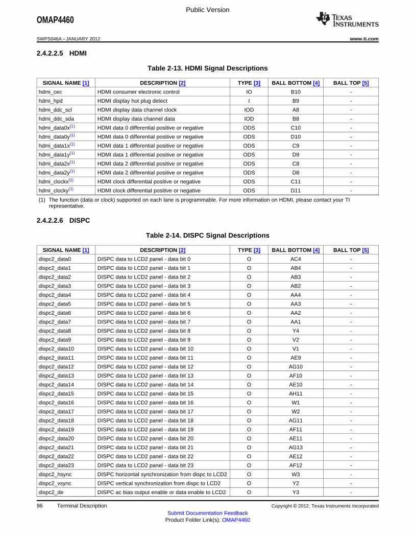
Public Version
OMAP4460
SWPS046A –JANUARY 2012 www.ti.com
2.4.2.2.5 HDMI
Table 2-13. HDMI Signal Descriptions
SIGNAL NAME [1] DESCRIPTION [2] TYPE [3] BALL BOTTOM [4] BALL TOP [5]
hdmi_cec HDMI consumer electronic control IO B10 -
hdmi_hpd HDMI display hot plug detect I B9 -
hdmi_ddc_scl HDMI display data channel clock IOD A8 -
hdmi_ddc_sda HDMI display data channel data IOD B8 -
hdmi_data0x(1) HDMI data 0 differential positive or negative ODS C10 -
hdmi_data0y(1) HDMI data 0 differential positive or negative ODS D10 -
hdmi_data1x(1) HDMI data 1 differential positive or negative ODS C9 -
hdmi_data1y(1) HDMI data 1 differential positive or negative ODS D9 -
hdmi_data2x(1) HDMI data 2 differential positive or negative ODS C8 -
hdmi_data2y(1) HDMI data 2 differential positive or negative ODS D8 -
hdmi_clockx(1) HDMI clock differential positive or negative ODS C11 -
hdmi_clocky(1) HDMI clock differential positive or negative ODS D11 -
(1) The function (data or clock) supported on each lane is programmable. For more information on HDMI, please contact your TIrepresentative.
2.4.2.2.6 DISPC
Table 2-14. DISPC Signal Descriptions
SIGNAL NAME [1] DESCRIPTION [2] TYPE [3] BALL BOTTOM [4] BALL TOP [5]
dispc2_data0 DISPC data to LCD2 panel - data bit 0 O AC4 -
dispc2_data1 DISPC data to LCD2 panel - data bit 1 O AB4 -
dispc2_data2 DISPC data to LCD2 panel - data bit 2 O AB3 -
dispc2_data3 DISPC data to LCD2 panel - data bit 3 O AB2 -
dispc2_data4 DISPC data to LCD2 panel - data bit 4 O AA4 -
dispc2_data5 DISPC data to LCD2 panel - data bit 5 O AA3 -
dispc2_data6 DISPC data to LCD2 panel - data bit 6 O AA2 -
dispc2_data7 DISPC data to LCD2 panel - data bit 7 O AA1 -
dispc2_data8 DISPC data to LCD2 panel - data bit 8 O Y4 -
dispc2_data9 DISPC data to LCD2 panel - data bit 9 O V2 -
dispc2_data10 DISPC data to LCD2 panel - data bit 10 O V1 -
dispc2_data11 DISPC data to LCD2 panel - data bit 11 O AE9 -
dispc2_data12 DISPC data to LCD2 panel - data bit 12 O AG10 -
dispc2_data13 DISPC data to LCD2 panel - data bit 13 O AF10 -
dispc2_data14 DISPC data to LCD2 panel - data bit 14 O AE10 -
dispc2_data15 DISPC data to LCD2 panel - data bit 15 O AH11 -
dispc2_data16 DISPC data to LCD2 panel - data bit 16 O W1 -
dispc2_data17 DISPC data to LCD2 panel - data bit 17 O W2 -
dispc2_data18 DISPC data to LCD2 panel - data bit 18 O AG11 -
dispc2_data19 DISPC data to LCD2 panel - data bit 19 O AF11 -
dispc2_data20 DISPC data to LCD2 panel - data bit 20 O AE11 -
dispc2_data21 DISPC data to LCD2 panel - data bit 21 O AG13 -
dispc2_data22 DISPC data to LCD2 panel - data bit 22 O AE12 -
dispc2_data23 DISPC data to LCD2 panel - data bit 23 O AF12 -
dispc2_hsync DISPC horizontal synchronization from dispc to LCD2 O W3 -
dispc2_vsync DISPC vertical synchronization from dispc to LCD2 O Y2 -
dispc2_de DISPC ac bias output enable or data enable to LCD2 O Y3 -
96 Terminal Description Copyright © 2012, Texas Instruments Incorporated
Submit Documentation FeedbackProduct Folder Link(s): OMAP4460

Public Version
OMAP4460
www.ti.com SWPS046A –JANUARY 2012
Table 2-14. DISPC Signal Descriptions (continued)
SIGNAL NAME [1] DESCRIPTION [2] TYPE [3] BALL BOTTOM [4] BALL TOP [5]
dispc2_pclk DISPC LCD pixel clock to LCD2 O W4 -
dispc2_fid DISPC field ID to LCD2 O P2 -
2.4.3 Serial Communication Interfaces
2.4.3.1 HDQ/1-Wire
NOTEFor more information, see the Serial Communication Interface / HDQ/1-Wire section of theOMAP4460 TRM.
Table 2-15. HDQ/1-Wire Signal Descriptions
SIGNAL NAME [1] DESCRIPTION [2] TYPE [3] BALL BOTTOM [4] BALL TOP [5]
hdq_sio HDQ ™ 1-Wire ® control and data interface IOD AA27 -
2.4.3.2 I2C
NOTEFor more information, see the Serial Communication Interface / Multimaster High-Speed I2CController / HS I2C Environment / HS I2C in I2C Mode section of the OMAP4460 TRM.
Table 2-16. I2C Signal Descriptions
SIGNAL NAME [1] DESCRIPTION [2] TYPE [3] BALL BOTTOM [4] BALL TOP [5]
Inter-Integrated Circuit Interface (I2C1)
i2c1_scl I2C1 clock OD AE28 -
i2c1_sda I2C1 data IOD AE26 -
Inter-Integrated Circuit Interface (I2C2)
i2c2_scl I2C2 clock OD C26 -
i2c2_sda I2C2 data IOD D26 -
i2c2_sccb I2C2 serial camera control bus OD AA27 -
Inter-Integrated Circuit Interface (I2C3)
i2c3_scl I2C3 clock OD W27 -
i2c3_sda I2C3 data IOD Y27 -
i2c3_sccb I2C3 serial camera control bus OD AA27 -
Inter-Integrated Circuit Interface (I2C4)
i2c4_scl I2C4 clock OD AG21 -
i2c4_sda I2C4 data IOD AH22 -
Copyright © 2012, Texas Instruments Incorporated Terminal Description 97Submit Documentation Feedback
Product Folder Link(s): OMAP4460
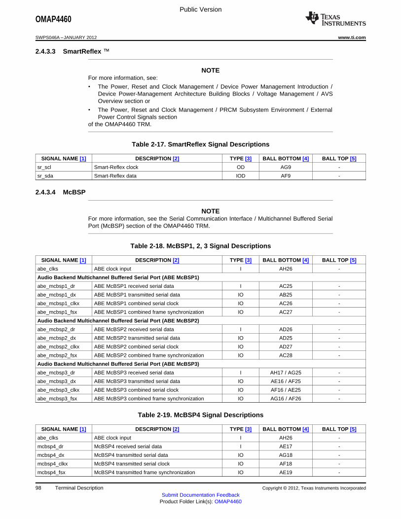
Public Version
OMAP4460
SWPS046A –JANUARY 2012 www.ti.com
2.4.3.3 SmartReflex ™
NOTEFor more information, see:
• The Power, Reset and Clock Management / Device Power Management Introduction /Device Power-Management Architecture Building Blocks / Voltage Management / AVSOverview section or
• The Power, Reset and Clock Management / PRCM Subsystem Environment / ExternalPower Control Signals section
of the OMAP4460 TRM.
Table 2-17. SmartReflex Signal Descriptions
SIGNAL NAME [1] DESCRIPTION [2] TYPE [3] BALL BOTTOM [4] BALL TOP [5]
sr_scl Smart-Reflex clock OD AG9 -
sr_sda Smart-Reflex data IOD AF9 -
2.4.3.4 McBSP
NOTEFor more information, see the Serial Communication Interface / Multichannel Buffered SerialPort (McBSP) section of the OMAP4460 TRM.
Table 2-18. McBSP1, 2, 3 Signal Descriptions
SIGNAL NAME [1] DESCRIPTION [2] TYPE [3] BALL BOTTOM [4] BALL TOP [5]
abe_clks ABE clock input I AH26 -
Audio Backend Multichannel Buffered Serial Port (ABE McBSP1)
abe_mcbsp1_dr ABE McBSP1 received serial data I AC25 -
abe_mcbsp1_dx ABE McBSP1 transmitted serial data IO AB25 -
abe_mcbsp1_clkx ABE McBSP1 combined serial clock IO AC26 -
abe_mcbsp1_fsx ABE McBSP1 combined frame synchronization IO AC27 -
Audio Backend Multichannel Buffered Serial Port (ABE McBSP2)
abe_mcbsp2_dr ABE McBSP2 received serial data I AD26 -
abe_mcbsp2_dx ABE McBSP2 transmitted serial data IO AD25 -
abe_mcbsp2_clkx ABE McBSP2 combined serial clock IO AD27 -
abe_mcbsp2_fsx ABE McBSP2 combined frame synchronization IO AC28 -
Audio Backend Multichannel Buffered Serial Port (ABE McBSP3)
abe_mcbsp3_dr ABE McBSP3 received serial data I AH17 / AG25 -
abe_mcbsp3_dx ABE McBSP3 transmitted serial data IO AE16 / AF25 -
abe_mcbsp3_clkx ABE McBSP3 combined serial clock IO AF16 / AE25 -
abe_mcbsp3_fsx ABE McBSP3 combined frame synchronization IO AG16 / AF26 -
Table 2-19. McBSP4 Signal Descriptions
SIGNAL NAME [1] DESCRIPTION [2] TYPE [3] BALL BOTTOM [4] BALL TOP [5]
abe_clks ABE clock input I AH26 -
mcbsp4_dr McBSP4 received serial data I AE17 -
mcbsp4_dx McBSP4 transmitted serial data IO AG18 -
mcbsp4_clkx McBSP4 transmitted serial clock IO AF18 -
mcbsp4_fsx McBSP4 transmitted frame synchronization IO AE19 -
98 Terminal Description Copyright © 2012, Texas Instruments Incorporated
Submit Documentation FeedbackProduct Folder Link(s): OMAP4460

Public Version
OMAP4460
www.ti.com SWPS046A –JANUARY 2012
Table 2-19. McBSP4 Signal Descriptions (continued)
SIGNAL NAME [1] DESCRIPTION [2] TYPE [3] BALL BOTTOM [4] BALL TOP [5]
mcbsp4_clkr McBSP4 received serial clock IO AG19 -
mcbsp4_fsr McBSP4 received frame synchronization IO AF19 -
2.4.3.5 PDM
NOTEFor more information, see the Serial Communication Interface / Multichannel PDM Controllersection of the OMAP4460 TRM.
Table 2-20. ABE McPDM Signal Descriptions
SIGNAL NAME [1] DESCRIPTION [2] TYPE [3] BALL BOTTOM [4] BALL TOP [5]
abe_clks ABE clock input I AH26 -
abe_pdm_ul_data ABE PDM data stream from TWL6030 PMIC to OMAP4460 I AG25 -
abe_pdm_dl_data ABE PDM data stream from OMAP4460 to TWL6030 PMIC O AF25 -
abe_pdm_frame ABE PDM Frame synchronization IO AE25 -
abe_pdm_lb_clk ABE PDM loop back clock O AF26 -
2.4.3.6 DMIC
NOTEFor more information, see the Serial Communication Interface / Digital Microphone Modulesection of the OMAP4460 TRM.
Table 2-21. ABE DMIC Signal Descriptions
SIGNAL NAME [1] DESCRIPTION [2] TYPE [3] BALL BOTTOM [4] BALL TOP [5]
abe_clks ABE clock input I AH26 -
abe_dmic_clk1 ABE digital microphone clock output 1 O AE24 -
abe_dmic_clk2 ABE digital microphone clock output 2 O AH24 -
abe_dmic_clk3 ABE digital microphone clock output 3 O AG16 -
abe_dmic_din1 ABE digital microphone data input 1 I AF24 -
abe_dmic_din2 ABE digital microphone data input 2 I AG24 -
abe_dmic_din3 ABE digital microphone data input 3 I AF16 / AH24 -
2.4.3.7 McASP
NOTEFor more information, see the Serial Communication Interface / Multichannel Audio SerialPort section of the OMAP4460 TRM.
Table 2-22. ABE McASP Signal Descriptions
SIGNAL NAME [1] DESCRIPTION [2] TYPE [3] BALL BOTTOM [4] BALL TOP [5]
abe_clks ABE clock input I AH26 -
abe_mcasp_axr ABE McASP serial data IO IO AD26 / AG24 -
abe_mcasp_aclkx ABE McASP clock transmit O AB25 -
abe_mcasp_afsx ABE McASP frame synchonization transmit O AC28 -
Copyright © 2012, Texas Instruments Incorporated Terminal Description 99Submit Documentation Feedback
Product Folder Link(s): OMAP4460

Public Version
OMAP4460
SWPS046A –JANUARY 2012 www.ti.com
Table 2-22. ABE McASP Signal Descriptions (continued)
SIGNAL NAME [1] DESCRIPTION [2] TYPE [3] BALL BOTTOM [4] BALL TOP [5]
abe_mcasp_ahclkx ABE McASP high frequency clock output O AD27 -
abe_mcasp_amutein ABE McASP auto mute input I AC27 -
abe_mcasp_amute ABE McASP auto mute output O AD25 -
2.4.3.8 SLIMbus ®
NOTEFor more information, see the Serial Communication Interface / Serial Low-Power Inter-ChipMedia Bus Controller section of the OMAP4460 TRM.
Table 2-23. ABE SLIMbus1 Signal Descriptions
SIGNAL NAME [1] DESCRIPTION [2] TYPE [3] BALL BOTTOM [4] BALL TOP [5]
abe_clks ABE clock input I AH26 -
abe_slimbus1_clock ABE SLIMbus1 clock IO AC26 -
abe_slimbus1_data ABE SLIMbus1 data IO AC25 -
Table 2-24. SLIMbus2 Signal Descriptions
SIGNAL NAME [1] DESCRIPTION [2] TYPE [3] BALL BOTTOM [4] BALL TOP [5]
abe_clks ABE clock input I AH26 -
slimbus2_clock SLIMbus2 clock IO AG24 / AG23 -
slimbus2_data SLIMbus2 data IO AH24 / AH23 -
2.4.3.9 HSI
NOTEFor more information, see the Serial Communication Interface / MIPI-HSI section of theOMAP4460 TRM.
Table 2-25. HSI Signal Descriptions
SIGNAL NAME [1] DESCRIPTION [2] TYPE [3] BALL BOTTOM [4] BALL TOP [5]
High-speed Synchronous Serial Interface (HSI1)
hsi1_cawake HSI1 cellular modem to APE wake signal I AE18 -
hsi1_cadata HSI1 cellular modem to APE signal I AG19 -
hsi1_caflag HSI1 cellular modem to APE flag signal I AF19 -
hsi1_acready HSI1 APE to cellular modem ready signal O AE19 -
hsi1_acwake HS1 APE to cellular modem wake signal O AF18 -
hsi1_acdata HSI1 APE to cellular modem data signal O AG18 -
hsi1_acflag HSI1 APE to cellular modem ready signal O AE17 -
hsi1_caready HSI1 cellular modem to APE ready signal I AF17 -
High-speed Synchronous Serial Interface (HSI2)
hsi2_cawake HSI2 cellular modem to APE wake signal I AG12 -
hsi2_cadata HSI2 cellular modem to APE signal I AF12 -
hsi2_caflag HSI2 cellular modem to APE flag signal I AE12 -
hsi2_acready HSI2 APE to cellular modem ready signal O AG13 -
hsi2_acwake HSI2 APE to cellular modem wake signal O AE11 -
100 Terminal Description Copyright © 2012, Texas Instruments Incorporated
Submit Documentation FeedbackProduct Folder Link(s): OMAP4460

Public Version
OMAP4460
www.ti.com SWPS046A –JANUARY 2012
Table 2-25. HSI Signal Descriptions (continued)
SIGNAL NAME [1] DESCRIPTION [2] TYPE [3] BALL BOTTOM [4] BALL TOP [5]
hsi2_acdata HSI2 APE to cellular modem data signal O AF11 -
hsi2_acflag HSI2 APE to cellular modem ready signal O AG11 -
hsi2_caready HSI2 cellular modem to APE ready signal I AH11 -
2.4.3.10 McSPI
NOTEFor more information, see the Serial Communication Interface / Multichannel Serial PortInterface (MCSPI) section of the OMAP4460 TRM.
Table 2-26. McSPI Signal Descriptions
SIGNAL NAME [1] DESCRIPTION [2] TYPE [3] BALL BOTTOM [4] BALL TOP [5]
Multichannel Serial Port Interface (McSPI1)
mcspi1_clk McSPI1 clock (slave input, master output) IO AF22 -
mcspi1_somi McSPI1 data (slave output, master input, Z when not shifting) IO AE22 -
mcspi1_simo McSPI1 data (slave input, master output, Z when not shifting) IO AG22 -
mcspi1_cs0 McSPI1 chip select 0 (slave input, master output) IO AE23 -
mcspi1_cs1 McSPI1 chip select 1 O AF23 -
mcspi1_cs2 McSPI1 chip select 2 O AG23 -
mcspi1_cs3 McSPI1 chip select 3 O AH23 -
Multichannel Serial Port Interface (McSPI2)
mcspi2_clk McSPI2 clock (slave input, master output) IO AD27 / AE5 -
mcspi2_somi McSPI2 data (slave output, master input, Z when not shifting) IO AD26 / AE4 -
mcspi2_simo McSPI2 data (slave input, master output, Z if not shifting) IO AD25 / AF5 -
mcspi2_cs0 McSPI2 chip select 0 (slave input, master output) IO AC28 / AF3 -
mcspi2_cs1 McSPI2 chip select 1 O AG3 -
Multichannel Serial Port Interface (McSPI3)
mcspi3_clk McSPI3 clock (slave input, master output) IO AE9 -
mcspi3_somi McSPI3 data (slave output, master input, Z when not shifting) IO AE10 -
mcspi3_simo McSPI3 data (slave input, master output, Z if not shifting) IO AG10 -
mcspi3_cs0 McSPI3 chip select 0 (slave input, master output) IO AF10 -
Multichannel Serial Port Interface (McSPI4)
mcspi4_clk McSPI4 clock (slave input, master output) IO AE21 -
mcspi4_somi McSPI4 data (slave output, master input, Z when not shifting) IO AF21 -
mcspi4_simo McSPI4 data (slave input, master output, Z if not shifting) IO AF20 -
mcspi4_cs0 McSPI4 chip select 0 (slave input, master output) IO AE20 -
2.4.3.11 UART
NOTEFor more information, see the Serial Communication Interface / UART/IrDA/CIR section ofthe OMAP4460 TRM.
Table 2-27. UART Signal Descriptions
SIGNAL NAME [1] DESCRIPTION [2] TYPE [3] BALL BOTTOM [4] BALL TOP [5]
Universal Asynchronous Receiver/Transmitter (UART1)
Copyright © 2012, Texas Instruments Incorporated Terminal Description 101Submit Documentation Feedback
Product Folder Link(s): OMAP4460

Public Version
OMAP4460
SWPS046A –JANUARY 2012 www.ti.com
Table 2-27. UART Signal Descriptions (continued)
SIGNAL NAME [1] DESCRIPTION [2] TYPE [3] BALL BOTTOM [4] BALL TOP [5]
uart1_cts UART1 clear to send I AG23 -
uart1_rts UART1 request to send O AH23 -
uart1_rx UART1 receive data I E3 / C26 / AF23 / -AA3
uart1_tx UART1 transmit data O D26 / F27 -
Universal Asynchronous Receiver/Transmitter (UART2)
uart2_cts UART2 clear to send I AB26 -
uart2_rts UART2 request to send O AB27 -
uart2_rx UART2 receive data I AA25 / B5 -
uart2_tx UART2 transmit data O AA26 / B4 -
Universal Asynchronous Receiver/Transmitter (UART3)
uart3_cts_rctx UART3 clear to send or remote control data output IO F27 / Y2 -
uart3_rts_sd UART3 request to send or infrared transceiver O F28 / W4 -shutdown
uart3_rx_irrx UART3 receive data input or infrared data input I G27 / B5 / W3 -
uart3_tx_irtx UART3 transmit data output or infrared data output O G28 / B4 / W2 -
Universal Asynchronous Receiver/Transmitter (UART4)
uart4_rx UART4 receive data I AG20 -
uart4_tx UART4 transmit data O AH19 -
uart4_cts UART4 clear to send I AE24 -
uart4_rts UART4 request to send O AF24 -
2.4.3.12 USB
NOTEFor more information, see:
• Serial Communication Interface / High-Speed Multiport USB Host Subsystem section, or
• Serial Communication Interface / High-Speed USB OTG Controller section, or
• Serial Communication Interface / Full-Speed USB Host Controller sectionof the OMAP4460 TRM.
Table 2-28. USB Signal Descriptions
SIGNAL NAME [1] DESCRIPTION [2] TYPE [3] BALL BOTTOM [4] BALL TOP [5]
Universal Serial Bus (USBA0)
usba0_ulpiphy_clk USBA0 IO to/from external transceiver 60-MHz clock I P2 -
usba0_ulpiphy_stp USBA0 output to external transceiver to stop data O V1 -stream
usba0_ulpiphy_dir USBA0 data direction control from external I V2 -transceiver
usba0_ulpiphy_nxt USBA0 next signal control from external transceiver I W1 -
usba0_ulpiphy_dat0 USBA0 data bit 0 to/from external transceiver IO W2 -
usba0_ulpiphy_dat1 USBA0 data bit 1 to/from external transceiver IO W3 -
usba0_ulpiphy_dat2 USBA0 data bit 2 to/from external transceiver IO W4 -
usba0_ulpiphy_dat3 USBA0 data bit 3 to/from external transceiver IO Y2 -
usba0_ulpiphy_dat4 USBA0 data bit 4 to/from external transceiver IO Y3 -
usba0_ulpiphy_dat5 USBA0 data bit 5 to/from external transceiver IO Y4 -
usba0_ulpiphy_dat6 USBA0 data bit 6 to/from external transceiver IO AA1 -
usba0_ulpiphy_dat7 USBA0 data bit 7 to/from external transceiver IO AA2 -
102 Terminal Description Copyright © 2012, Texas Instruments Incorporated
Submit Documentation FeedbackProduct Folder Link(s): OMAP4460
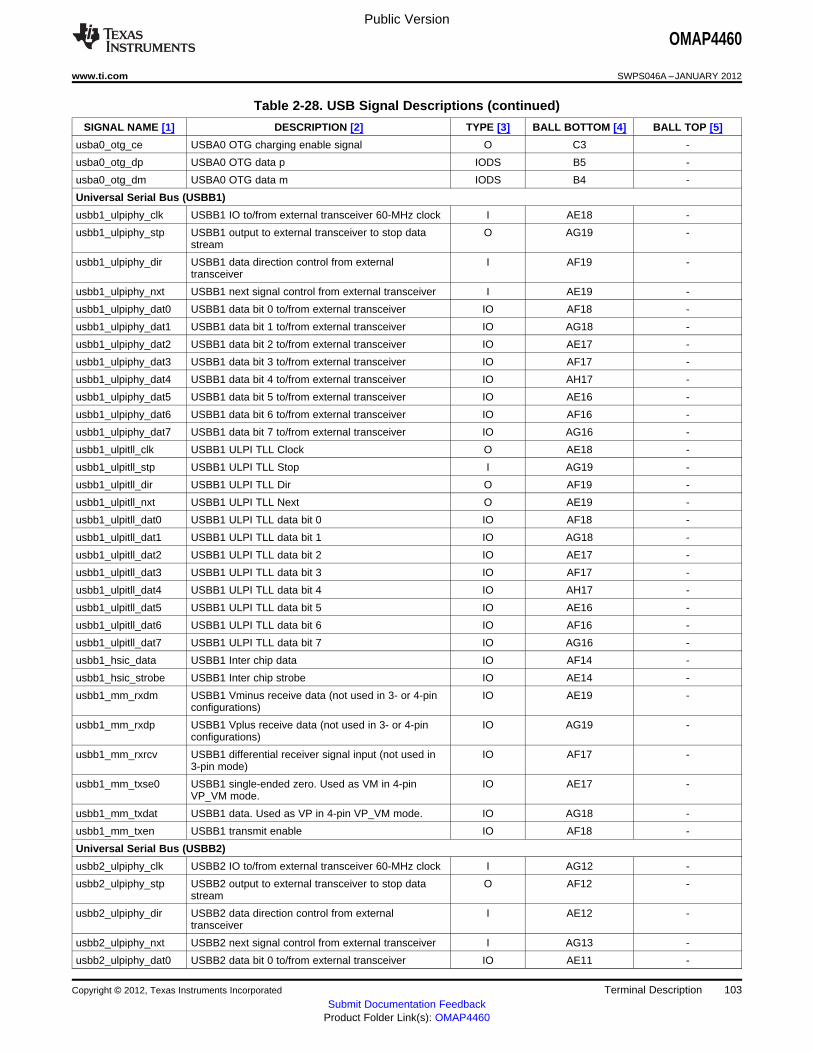
Public Version
OMAP4460
www.ti.com SWPS046A –JANUARY 2012
Table 2-28. USB Signal Descriptions (continued)
SIGNAL NAME [1] DESCRIPTION [2] TYPE [3] BALL BOTTOM [4] BALL TOP [5]
usba0_otg_ce USBA0 OTG charging enable signal O C3 -
usba0_otg_dp USBA0 OTG data p IODS B5 -
usba0_otg_dm USBA0 OTG data m IODS B4 -
Universal Serial Bus (USBB1)
usbb1_ulpiphy_clk USBB1 IO to/from external transceiver 60-MHz clock I AE18 -
usbb1_ulpiphy_stp USBB1 output to external transceiver to stop data O AG19 -stream
usbb1_ulpiphy_dir USBB1 data direction control from external I AF19 -transceiver
usbb1_ulpiphy_nxt USBB1 next signal control from external transceiver I AE19 -
usbb1_ulpiphy_dat0 USBB1 data bit 0 to/from external transceiver IO AF18 -
usbb1_ulpiphy_dat1 USBB1 data bit 1 to/from external transceiver IO AG18 -
usbb1_ulpiphy_dat2 USBB1 data bit 2 to/from external transceiver IO AE17 -
usbb1_ulpiphy_dat3 USBB1 data bit 3 to/from external transceiver IO AF17 -
usbb1_ulpiphy_dat4 USBB1 data bit 4 to/from external transceiver IO AH17 -
usbb1_ulpiphy_dat5 USBB1 data bit 5 to/from external transceiver IO AE16 -
usbb1_ulpiphy_dat6 USBB1 data bit 6 to/from external transceiver IO AF16 -
usbb1_ulpiphy_dat7 USBB1 data bit 7 to/from external transceiver IO AG16 -
usbb1_ulpitll_clk USBB1 ULPI TLL Clock O AE18 -
usbb1_ulpitll_stp USBB1 ULPI TLL Stop I AG19 -
usbb1_ulpitll_dir USBB1 ULPI TLL Dir O AF19 -
usbb1_ulpitll_nxt USBB1 ULPI TLL Next O AE19 -
usbb1_ulpitll_dat0 USBB1 ULPI TLL data bit 0 IO AF18 -
usbb1_ulpitll_dat1 USBB1 ULPI TLL data bit 1 IO AG18 -
usbb1_ulpitll_dat2 USBB1 ULPI TLL data bit 2 IO AE17 -
usbb1_ulpitll_dat3 USBB1 ULPI TLL data bit 3 IO AF17 -
usbb1_ulpitll_dat4 USBB1 ULPI TLL data bit 4 IO AH17 -
usbb1_ulpitll_dat5 USBB1 ULPI TLL data bit 5 IO AE16 -
usbb1_ulpitll_dat6 USBB1 ULPI TLL data bit 6 IO AF16 -
usbb1_ulpitll_dat7 USBB1 ULPI TLL data bit 7 IO AG16 -
usbb1_hsic_data USBB1 Inter chip data IO AF14 -
usbb1_hsic_strobe USBB1 Inter chip strobe IO AE14 -
usbb1_mm_rxdm USBB1 Vminus receive data (not used in 3- or 4-pin IO AE19 -configurations)
usbb1_mm_rxdp USBB1 Vplus receive data (not used in 3- or 4-pin IO AG19 -configurations)
usbb1_mm_rxrcv USBB1 differential receiver signal input (not used in IO AF17 -3-pin mode)
usbb1_mm_txse0 USBB1 single-ended zero. Used as VM in 4-pin IO AE17 -VP_VM mode.
usbb1_mm_txdat USBB1 data. Used as VP in 4-pin VP_VM mode. IO AG18 -
usbb1_mm_txen USBB1 transmit enable IO AF18 -
Universal Serial Bus (USBB2)
usbb2_ulpiphy_clk USBB2 IO to/from external transceiver 60-MHz clock I AG12 -
usbb2_ulpiphy_stp USBB2 output to external transceiver to stop data O AF12 -stream
usbb2_ulpiphy_dir USBB2 data direction control from external I AE12 -transceiver
usbb2_ulpiphy_nxt USBB2 next signal control from external transceiver I AG13 -
usbb2_ulpiphy_dat0 USBB2 data bit 0 to/from external transceiver IO AE11 -
Copyright © 2012, Texas Instruments Incorporated Terminal Description 103Submit Documentation Feedback
Product Folder Link(s): OMAP4460

Public Version
OMAP4460
SWPS046A –JANUARY 2012 www.ti.com
Table 2-28. USB Signal Descriptions (continued)
SIGNAL NAME [1] DESCRIPTION [2] TYPE [3] BALL BOTTOM [4] BALL TOP [5]
usbb2_ulpiphy_dat1 USBB2 data bit 1 to/from external transceiver IO AF11 -
usbb2_ulpiphy_dat2 USBB2 data bit 2 to/from external transceiver IO AG11 -
usbb2_ulpiphy_dat3 USBB2 data bit 3 to/from external transceiver IO AH11 -
usbb2_ulpiphy_dat4 USBB2 data bit 4 to/from external transceiver IO AE10 -
usbb2_ulpiphy_dat5 USBB2 data bit 5 to/from external transceiver IO AF10 -
usbb2_ulpiphy_dat6 USBB2 data bit 6 to/from external transceiver IO AG10 -
usbb2_ulpiphy_dat7 USBB2 data bit 7 to/from external transceiver IO AE9 -
usbb2_ulpitll_clk USBB2 ULPI TLL Clock O AG12 -
usbb2_ulpitll_stp USBB2 ULPI TLL Stop I AF12 -
usbb2_ulpitll_dir USBB2 ULPI TLL Dir O AE12 -
usbb2_ulpitll_nxt USBB2 ULPI TLL Next O AG13 -
usbb2_ulpitll_dat0 USBB2 ULPI TLL data bit 0 IO AE11 -
usbb2_ulpitll_dat1 USBB2 ULPI TLL data bit 1 IO AF11 -
usbb2_ulpitll_dat2 USBB2 ULPI TLL data bit 2 IO AG11 -
usbb2_ulpitll_dat3 USBB2 ULPI TLL data bit 3 IO AH11 -
usbb2_ulpitll_dat4 USBB2 ULPI TLL data bit 4 IO AE10 -
usbb2_ulpitll_dat5 USBB2 ULPI TLL data bit 5 IO AF10 -
usbb2_ulpitll_dat6 USBB2 ULPI TLL data bit 6 IO AG10 -
usbb2_ulpitll_dat7 USBB2 ULPI TLL data bit 7 IO AE9 -
usbb2_hsic_data USBB2 Inter chip data IO AF13 -
usbb2_hsic_strobe USBB2 Inter chip strobe IO AE13 -
usbb2_mm_rxdm USBB2 Vminus receive data (not used in 3- or 4-pin IO AD27 -configurations)
usbb2_mm_rxdp USBB2 Vplus receive data (not used in 3- or 4-pin IO AD26 -configurations)
usbb2_mm_rxrcv USBB2 differential receiver signal input (not used in IO AD25 -3-pin mode)
usbb2_mm_txse0 USBB2 single-ended zero. Used as VM in 4-pin IO AE24 / AG11 -VP_VM mode.
usbb2_mm_txdat USBB2 data. Used as VP in 4-pin VP_VM mode. IO AF24 / AF11 -
usbb2_mm_txen USBB2 transmit enable IO AC28 / AE11 -
Universal Serial Bus (USBC1)
usbc1_icusb_dp USBC1 interchip USB host D plus IODS H2 / AE5 -
usbc1_icusb_dm USBC1 interchip USB host D minus IODS H3 / AF5 -
usbc1_icusb_txen USBC1 transmit enable O D23 / AF4 -
usbc1_icusb_rcv USBC1 receive I AE4 -
2.4.4 Removable Media Interfaces
2.4.4.1 MMC/SDIO
NOTEFor more information, see the MMC/SD/SDIO section of the OMAP4460 TRM.
Table 2-29. MMC/SDIO Signal Descriptions
SIGNAL NAME [1] DESCRIPTION [2] TYPE [3] BALL BOTTOM [4] BALL TOP [5]
Multimedia Memory Card / Secure Digital IO (SDMMC1)
sdmmc1_clk SDMMC1 clock O D25 / D2 -
104 Terminal Description Copyright © 2012, Texas Instruments Incorporated
Submit Documentation FeedbackProduct Folder Link(s): OMAP4460
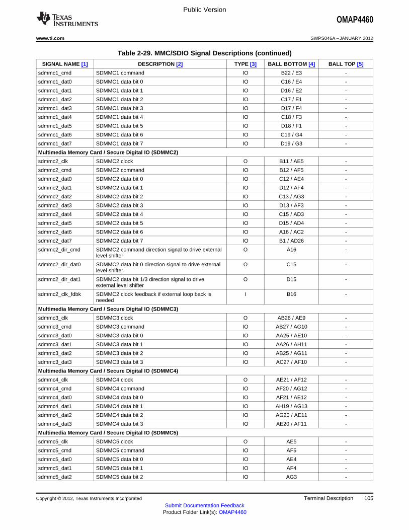
Public Version
OMAP4460
www.ti.com SWPS046A –JANUARY 2012
Table 2-29. MMC/SDIO Signal Descriptions (continued)
SIGNAL NAME [1] DESCRIPTION [2] TYPE [3] BALL BOTTOM [4] BALL TOP [5]
sdmmc1_cmd SDMMC1 command IO B22 / E3 -
sdmmc1_dat0 SDMMC1 data bit 0 IO C16 / E4 -
sdmmc1_dat1 SDMMC1 data bit 1 IO D16 / E2 -
sdmmc1_dat2 SDMMC1 data bit 2 IO C17 / E1 -
sdmmc1_dat3 SDMMC1 data bit 3 IO D17 / F4 -
sdmmc1_dat4 SDMMC1 data bit 4 IO C18 / F3 -
sdmmc1_dat5 SDMMC1 data bit 5 IO D18 / F1 -
sdmmc1_dat6 SDMMC1 data bit 6 IO C19 / G4 -
sdmmc1_dat7 SDMMC1 data bit 7 IO D19 / G3 -
Multimedia Memory Card / Secure Digital IO (SDMMC2)
sdmmc2_clk SDMMC2 clock O B11 / AE5 -
sdmmc2_cmd SDMMC2 command IO B12 / AF5 -
sdmmc2_dat0 SDMMC2 data bit 0 IO C12 / AE4 -
sdmmc2_dat1 SDMMC2 data bit 1 IO D12 / AF4 -
sdmmc2_dat2 SDMMC2 data bit 2 IO C13 / AG3 -
sdmmc2_dat3 SDMMC2 data bit 3 IO D13 / AF3 -
sdmmc2_dat4 SDMMC2 data bit 4 IO C15 / AD3 -
sdmmc2_dat5 SDMMC2 data bit 5 IO D15 / AD4 -
sdmmc2_dat6 SDMMC2 data bit 6 IO A16 / AC2 -
sdmmc2_dat7 SDMMC2 data bit 7 IO B1 / AD26 -
sdmmc2_dir_cmd SDMMC2 command direction signal to drive external O A16 -level shifter
sdmmc2_dir_dat0 SDMMC2 data bit 0 direction signal to drive external O C15 -level shifter
sdmmc2_dir_dat1 SDMMC2 data bit 1/3 direction signal to drive O D15 -external level shifter
sdmmc2_clk_fdbk SDMMC2 clock feedback if external loop back is I B16 -needed
Multimedia Memory Card / Secure Digital IO (SDMMC3)
sdmmc3_clk SDMMC3 clock O AB26 / AE9 -
sdmmc3_cmd SDMMC3 command IO AB27 / AG10 -
sdmmc3_dat0 SDMMC3 data bit 0 IO AA25 / AE10 -
sdmmc3_dat1 SDMMC3 data bit 1 IO AA26 / AH11 -
sdmmc3_dat2 SDMMC3 data bit 2 IO AB25 / AG11 -
sdmmc3_dat3 SDMMC3 data bit 3 IO AC27 / AF10 -
Multimedia Memory Card / Secure Digital IO (SDMMC4)
sdmmc4_clk SDMMC4 clock O AE21 / AF12 -
sdmmc4_cmd SDMMC4 command IO AF20 / AG12 -
sdmmc4_dat0 SDMMC4 data bit 0 IO AF21 / AE12 -
sdmmc4_dat1 SDMMC4 data bit 1 IO AH19 / AG13 -
sdmmc4_dat2 SDMMC4 data bit 2 IO AG20 / AE11 -
sdmmc4_dat3 SDMMC4 data bit 3 IO AE20 / AF11 -
Multimedia Memory Card / Secure Digital IO (SDMMC5)
sdmmc5_clk SDMMC5 clock O AE5 -
sdmmc5_cmd SDMMC5 command IO AF5 -
sdmmc5_dat0 SDMMC5 data bit 0 IO AE4 -
sdmmc5_dat1 SDMMC5 data bit 1 IO AF4 -
sdmmc5_dat2 SDMMC5 data bit 2 IO AG3 -
Copyright © 2012, Texas Instruments Incorporated Terminal Description 105Submit Documentation Feedback
Product Folder Link(s): OMAP4460
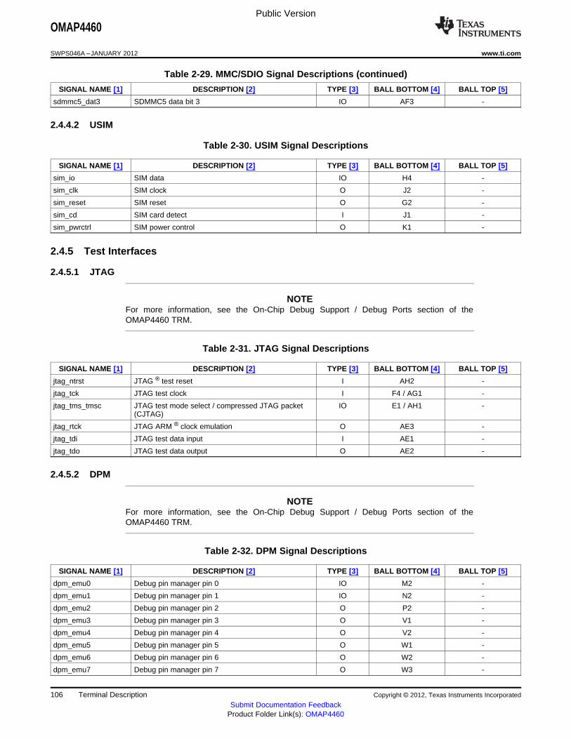
Public Version
OMAP4460
SWPS046A –JANUARY 2012 www.ti.com
Table 2-29. MMC/SDIO Signal Descriptions (continued)
SIGNAL NAME [1] DESCRIPTION [2] TYPE [3] BALL BOTTOM [4] BALL TOP [5]
sdmmc5_dat3 SDMMC5 data bit 3 IO AF3 -
2.4.4.2 USIM
Table 2-30. USIM Signal Descriptions
SIGNAL NAME [1] DESCRIPTION [2] TYPE [3] BALL BOTTOM [4] BALL TOP [5]
sim_io SIM data IO H4 -
sim_clk SIM clock O J2 -
sim_reset SIM reset O G2 -
sim_cd SIM card detect I J1 -
sim_pwrctrl SIM power control O K1 -
2.4.5 Test Interfaces
2.4.5.1 JTAG
NOTEFor more information, see the On-Chip Debug Support / Debug Ports section of theOMAP4460 TRM.
Table 2-31. JTAG Signal Descriptions
SIGNAL NAME [1] DESCRIPTION [2] TYPE [3] BALL BOTTOM [4] BALL TOP [5]
jtag_ntrst JTAG ® test reset I AH2 -
jtag_tck JTAG test clock I F4 / AG1 -
jtag_tms_tmsc JTAG test mode select / compressed JTAG packet IO E1 / AH1 -(CJTAG)
jtag_rtck JTAG ARM ® clock emulation O AE3 -
jtag_tdi JTAG test data input I AE1 -
jtag_tdo JTAG test data output O AE2 -
2.4.5.2 DPM
NOTEFor more information, see the On-Chip Debug Support / Debug Ports section of theOMAP4460 TRM.
Table 2-32. DPM Signal Descriptions
SIGNAL NAME [1] DESCRIPTION [2] TYPE [3] BALL BOTTOM [4] BALL TOP [5]
dpm_emu0 Debug pin manager pin 0 IO M2 -
dpm_emu1 Debug pin manager pin 1 IO N2 -
dpm_emu2 Debug pin manager pin 2 O P2 -
dpm_emu3 Debug pin manager pin 3 O V1 -
dpm_emu4 Debug pin manager pin 4 O V2 -
dpm_emu5 Debug pin manager pin 5 O W1 -
dpm_emu6 Debug pin manager pin 6 O W2 -
dpm_emu7 Debug pin manager pin 7 O W3 -
106 Terminal Description Copyright © 2012, Texas Instruments Incorporated
Submit Documentation FeedbackProduct Folder Link(s): OMAP4460
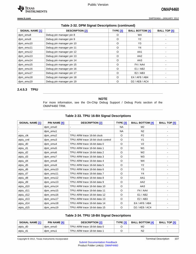
Public Version
OMAP4460
www.ti.com SWPS046A –JANUARY 2012
Table 2-32. DPM Signal Descriptions (continued)
SIGNAL NAME [1] DESCRIPTION [2] TYPE [3] BALL BOTTOM [4] BALL TOP [5]
dpm_emu8 Debug pin manager pin 8 O W4 -
dpm_emu9 Debug pin manager pin 9 O Y2 -
dpm_emu10 Debug pin manager pin 10 O Y3 -
dpm_emu11 Debug pin manager pin 11 O Y4 -
dpm_emu12 Debug pin manager pin 12 O AA1 -
dpm_emu13 Debug pin manager pin 13 O AA2 -
dpm_emu14 Debug pin manager pin 14 O AA3 -
dpm_emu15 Debug pin manager pin 15 O F4 / AA4 -
dpm_emu16 Debug pin manager pin 16 O E1 / AB2 -
dpm_emu17 Debug pin manager pin 17 O E2 / AB3 -
dpm_emu18 Debug pin manager pin 18 O E4 / AF8 / AB4 -
dpm_emu19 Debug pin manager pin 19 O D2 / AE8 / AC4 -
2.4.5.3 TPIU
NOTEFor more information, see the On-Chip Debug Support / Debug Ports section of theOMAP4460 TRM.
Table 2-33. TPIU 16-Bit Signal Descriptions
SIGNAL NAME [1] PIN NAME [6] DESCRIPTION [2] TYPE [3] BALL BOTTOM [4] BALL TOP [5]
- dpm_emu0 - NA M2 -
- dpm_emu1 - NA N2 -
atpiu_clk dpm_emu2 TPIU ARM trace 16-bit clock O P2 -
atpiu_cntl dpm_emu3 TPIU ARM trace 16-bit clock control O V1 -
atpiu_d0 dpm_emu4 TPIU ARM trace 16-bit data 0 O V2 -
atpiu_d1 dpm_emu5 TPIU ARM trace 16-bit data 1 O W1 -
atpiu_d2 dpm_emu6 TPIU ARM trace 16-bit data 2 O W2 -
atpiu_d3 dpm_emu7 TPIU ARM trace 16-bit data 3 O W3 -
atpiu_d4 dpm_emu8 TPIU ARM trace 16-bit data 4 O W4 -
atpiu_d5 dpm_emu9 TPIU ARM trace 16-bit data 5 O Y2 -
atpiu_d6 dpm_emu10 TPIU ARM trace 16-bit data 6 O Y3 -
atpiu_d7 dpm_emu11 TPIU ARM trace 16-bit data 7 O Y4 -
atpiu_d8 dpm_emu12 TPIU ARM trace 16-bit data 8 O AA1 -
atpiu_d9 dpm_emu13 TPIU ARM trace 16-bit data 9 O AA2 -
atpiu_d10 dpm_emu14 TPIU ARM trace 16-bit data 10 O AA3 -
atpiu_d11 dpm_emu15 TPIU ARM trace 16-bit data 11 O F4 / AA4 -
atpiu_d12 dpm_emu16 TPIU ARM trace 16-bit data 12 O E1 / AB2 -
atpiu_d13 dpm_emu17 TPIU ARM trace 16-bit data 13 O E2 / AB3 -
atpiu_d14 dpm_emu18 TPIU ARM trace 16-bit data 14 O E4 / AF8 / AB4 -
atpiu_d15 dpm_emu19 TPIU ARM trace 16-bit data 15 O D2 / AE8 / AC4 -
Table 2-34. TPIU 18-Bit Signal Descriptions
SIGNAL NAME [1] PIN NAME [6] DESCRIPTION [2] TYPE [3] BALL BOTTOM [4] BALL TOP [5]
atpiu_d0 dpm_emu0 TPIU ARM trace 18-bit data 0 O M2 -
atpiu_d1 dpm_emu1 TPIU ARM trace 18-bit data 1 O N2 -
Copyright © 2012, Texas Instruments Incorporated Terminal Description 107Submit Documentation Feedback
Product Folder Link(s): OMAP4460
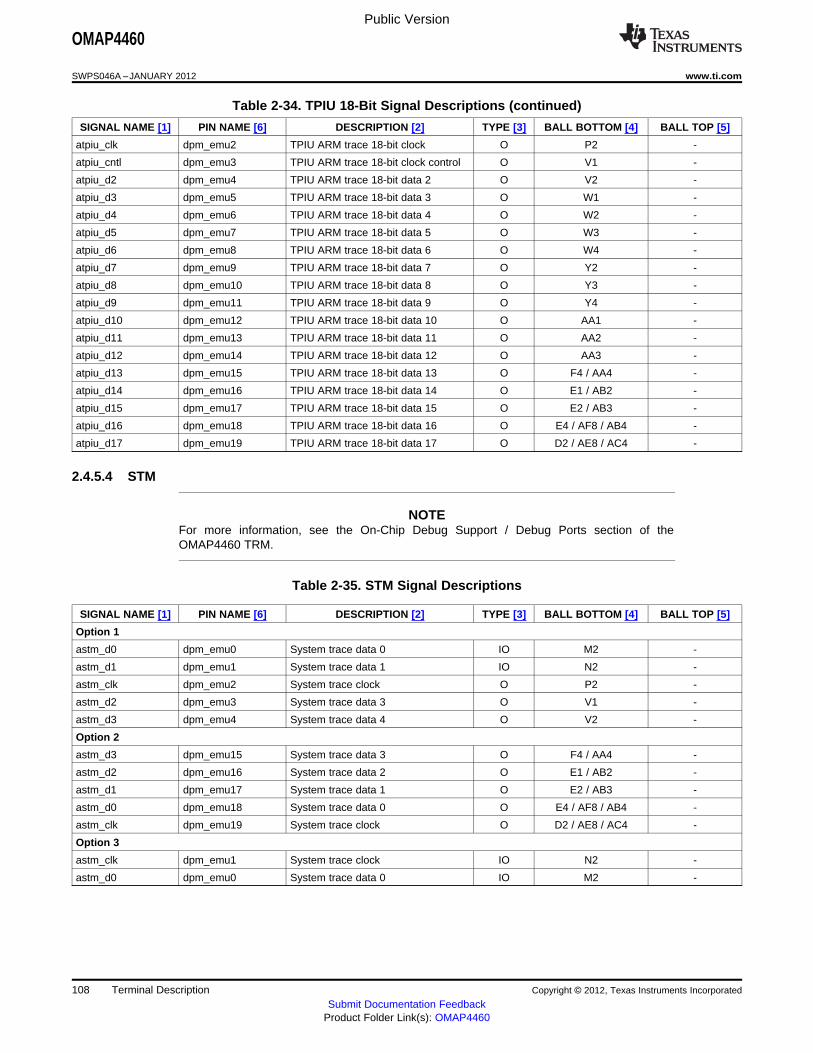
Public Version
OMAP4460
SWPS046A –JANUARY 2012 www.ti.com
Table 2-34. TPIU 18-Bit Signal Descriptions (continued)
SIGNAL NAME [1] PIN NAME [6] DESCRIPTION [2] TYPE [3] BALL BOTTOM [4] BALL TOP [5]
atpiu_clk dpm_emu2 TPIU ARM trace 18-bit clock O P2 -
atpiu_cntl dpm_emu3 TPIU ARM trace 18-bit clock control O V1 -
atpiu_d2 dpm_emu4 TPIU ARM trace 18-bit data 2 O V2 -
atpiu_d3 dpm_emu5 TPIU ARM trace 18-bit data 3 O W1 -
atpiu_d4 dpm_emu6 TPIU ARM trace 18-bit data 4 O W2 -
atpiu_d5 dpm_emu7 TPIU ARM trace 18-bit data 5 O W3 -
atpiu_d6 dpm_emu8 TPIU ARM trace 18-bit data 6 O W4 -
atpiu_d7 dpm_emu9 TPIU ARM trace 18-bit data 7 O Y2 -
atpiu_d8 dpm_emu10 TPIU ARM trace 18-bit data 8 O Y3 -
atpiu_d9 dpm_emu11 TPIU ARM trace 18-bit data 9 O Y4 -
atpiu_d10 dpm_emu12 TPIU ARM trace 18-bit data 10 O AA1 -
atpiu_d11 dpm_emu13 TPIU ARM trace 18-bit data 11 O AA2 -
atpiu_d12 dpm_emu14 TPIU ARM trace 18-bit data 12 O AA3 -
atpiu_d13 dpm_emu15 TPIU ARM trace 18-bit data 13 O F4 / AA4 -
atpiu_d14 dpm_emu16 TPIU ARM trace 18-bit data 14 O E1 / AB2 -
atpiu_d15 dpm_emu17 TPIU ARM trace 18-bit data 15 O E2 / AB3 -
atpiu_d16 dpm_emu18 TPIU ARM trace 18-bit data 16 O E4 / AF8 / AB4 -
atpiu_d17 dpm_emu19 TPIU ARM trace 18-bit data 17 O D2 / AE8 / AC4 -
2.4.5.4 STM
NOTEFor more information, see the On-Chip Debug Support / Debug Ports section of theOMAP4460 TRM.
Table 2-35. STM Signal Descriptions
SIGNAL NAME [1] PIN NAME [6] DESCRIPTION [2] TYPE [3] BALL BOTTOM [4] BALL TOP [5]
Option 1
astm_d0 dpm_emu0 System trace data 0 IO M2 -
astm_d1 dpm_emu1 System trace data 1 IO N2 -
astm_clk dpm_emu2 System trace clock O P2 -
astm_d2 dpm_emu3 System trace data 3 O V1 -
astm_d3 dpm_emu4 System trace data 4 O V2 -
Option 2
astm_d3 dpm_emu15 System trace data 3 O F4 / AA4 -
astm_d2 dpm_emu16 System trace data 2 O E1 / AB2 -
astm_d1 dpm_emu17 System trace data 1 O E2 / AB3 -
astm_d0 dpm_emu18 System trace data 0 O E4 / AF8 / AB4 -
astm_clk dpm_emu19 System trace clock O D2 / AE8 / AC4 -
Option 3
astm_clk dpm_emu1 System trace clock IO N2 -
astm_d0 dpm_emu0 System trace data 0 IO M2 -
108 Terminal Description Copyright © 2012, Texas Instruments Incorporated
Submit Documentation FeedbackProduct Folder Link(s): OMAP4460

Public Version
OMAP4460
www.ti.com SWPS046A –JANUARY 2012
2.4.5.5 ATTILA
Table 2-36. ATTILA Signal Descriptions
SIGNAL NAME [1] DESCRIPTION [2] TYPE [3] BALL BOTTOM [4] BALL TOP [5]
attila_hw_dbg0 Attila hardware debug pin 0 O M2 -
attila_hw_dbg1 Attila hardware debug pin 1 O H4 / N2 -
attila_hw_dbg2 Attila hardware debug pin 2 O J2 / P2 -
attila_hw_dbg3 Attila hardware debug pin 3 O G2 / V1 -
attila_hw_dbg4 Attila hardware debug pin 4 O J1 / V2 -
attila_hw_dbg5 Attila hardware debug pin 5 O K1 / W1 -
attila_hw_dbg6 Attila hardware debug pin 6 O AD2 / W2 -
attila_hw_dbg7 Attila hardware debug pin 7 O AD3 / W3 -
attila_hw_dbg8 Attila hardware debug pin 8 O AD4 / W4 -
attila_hw_dbg9 Attila hardware debug pin 9 O AC2 / Y2 -
attila_hw_dbg10 Attila hardware debug pin 10 O AC3 / Y3 -
attila_hw_dbg11 Attila hardware debug pin 11 O AG6 / Y4 -
attila_hw_dbg12 Attila hardware debug pin 12 O AF8 / AA1 -
attila_hw_dbg13 Attila hardware debug pin 13 O AE8 / AA2 -
attila_hw_dbg14 Attila hardware debug pin 14 O AA3 -
attila_hw_dbg15 Attila hardware debug pin 15 O AA4 -
attila_hw_dbg16 Attila hardware debug pin 16 O AB2 -
attila_hw_dbg17 Attila hardware debug pin 17 O AB3 -
attila_hw_dbg18 Attila hardware debug pin 18 O AB4 -
attila_hw_dbg19 Attila hardware debug pin 19 O AC4 -
attila_hw_dbg20 Attila hardware debug pin 20 O AE18 -
attila_hw_dbg21 Attila hardware debug pin 21 O AG19 -
attila_hw_dbg22 Attila hardware debug pin 22 O AF19 -
attila_hw_dbg23 Attila hardware debug pin 23 O AE19 -
attila_hw_dbg24 Attila hardware debug pin 24 O AF18 -
attila_hw_dbg25 Attila hardware debug pin 25 O AG18 -
attila_hw_dbg26 Attila hardware debug pin 26 O AE17 -
attila_hw_dbg27 Attila hardware debug pin 27 O AF17 -
attila_hw_dbg28 Attila hardware debug pin 28 O AH17 -
attila_hw_dbg29 Attila hardware debug pin 29 O AE16 -
attila_hw_dbg30 Attila hardware debug pin 30 O AF16 -
attila_hw_dbg31 Attila hardware debug pin 31 O AG16 -
2.4.5.6 Video Encoder Test
NOTEFor more information, see the Display Subsystem / Video Encoder section of the OMAP4460TRM.
Table 2-37. Video Encoder Test Signal Descriptions
SIGNAL NAME [1] DESCRIPTION [2] TYPE [3] BALL BOTTOM [4] BALL TOP [5]
venc_656_data0 Video encoder display debug signal 0 I B17 -
venc_656_data1 Video encoder display debug signal 1 I A18 -
venc_656_data2 Video encoder display debug signal 2 I B18 -
Copyright © 2012, Texas Instruments Incorporated Terminal Description 109Submit Documentation Feedback
Product Folder Link(s): OMAP4460

Public Version
OMAP4460
SWPS046A –JANUARY 2012 www.ti.com
Table 2-37. Video Encoder Test Signal Descriptions (continued)
SIGNAL NAME [1] DESCRIPTION [2] TYPE [3] BALL BOTTOM [4] BALL TOP [5]
venc_656_data3 Video encoder display debug signal 3 I A19 -
venc_656_data4 Video encoder display debug signal 4 I B19 -
venc_656_data5 Video encoder display debug signal 5 I B20 -
venc_656_data6 Video encoder display debug signal 6 I A21 -
venc_656_data7 Video encoder display debug signal 7 I B21 -
2.4.6 General-Purpose IOs
NOTEFor more information, see the General-Purpose Interface section of the OMAP4460 TRM.
Table 2-38. GPIO Signal Descriptions
SIGNAL NAME [1] DESCRIPTION [2] TYPE [3] BALL BOTTOM [4] BALL TOP [5]
gpio_wk0 General-purpose IO 0, Bank1, always GPIO IO H4 -
gpio_0 General-purpose IO 0, Bank1 IO J27 -
gpio_wk1 General-purpose IO 1, Bank1, always GPIO IO J2 -
gpio_1 General-purpose IO 1, Bank1 IO H27 -
gpio_wk2 General-purpose IO 2, Bank1, always GPIO IO G2 -
gpio_2 General-purpose IO 2, Bank1 IO L27 -
gpio_wk3 General-purpose IO 3, Bank1, always GPIO IO J1 -
gpio_3 General-purpose IO 3, Bank1 IO K27 -
gpio_wk4 General-purpose IO 4, Bank1, always GPIO IO K1 -
gpio_wk6 General-purpose IO 5, Bank1, always GPIO IO AD2 -
gpio_wk7 General-purpose IO 6, Bank1, always GPIO IO AC2 -
gpio_wk8 General-purpose IO 7, Bank1, always GPIO IO AC3 -
gpio_wk9 General-purpose IO 8, Bank1, always GPIO IO AF8 -
gpio_wk10 General-purpose IO 9, Bank1, always GPIO IO AE8 -
gpio_11 General-purpose IO 11, Bank1 IO M2 -
gpio_12 General-purpose IO 12, Bank1 IO N2 -
gpio_13 General-purpose IO 13, Bank1 IO P2 -
gpio_14 General-purpose IO 14, Bank1 IO V1 -
gpio_15 General-purpose IO 15, Bank1 IO V2 -
gpio_16 General-purpose IO 16, Bank1 IO W1 -
gpio_17 General-purpose IO 17, Bank1 IO W2 -
gpio_18 General-purpose IO 18, Bank1 IO W3 -
gpio_19 General-purpose IO 19, Bank1 IO W4 -
gpio_20 General-purpose IO 20, Bank1 IO Y2 -
gpio_21 General-purpose IO 21, Bank1 IO Y3 -
gpio_22 General-purpose IO 22, Bank1 IO Y4 -
gpio_23 General-purpose IO 23, Bank1 IO AA1 -
gpio_24 General-purpose IO 24, Bank1 IO AA2 -
gpio_25 General-purpose IO 25, Bank1 IO AA3 -
gpio_26 General-purpose IO 26, Bank1 IO AA4 -
gpio_27 General-purpose IO 27, Bank1 IO AB2 -
gpio_28 General-purpose IO 28, Bank1 IO AB3 -
gpio_wk29 General-purpose IO 29, Bank1, always GPIO IO AG6 -
110 Terminal Description Copyright © 2012, Texas Instruments Incorporated
Submit Documentation FeedbackProduct Folder Link(s): OMAP4460
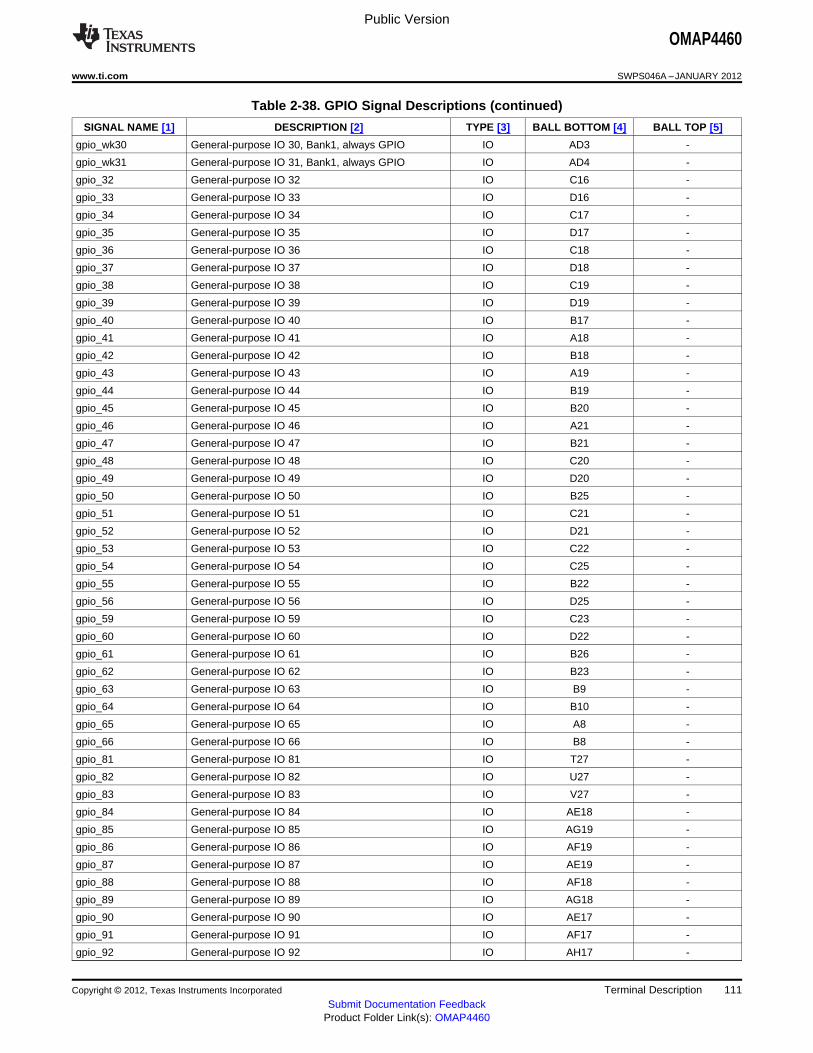
Public Version
OMAP4460
www.ti.com SWPS046A –JANUARY 2012
Table 2-38. GPIO Signal Descriptions (continued)
SIGNAL NAME [1] DESCRIPTION [2] TYPE [3] BALL BOTTOM [4] BALL TOP [5]
gpio_wk30 General-purpose IO 30, Bank1, always GPIO IO AD3 -
gpio_wk31 General-purpose IO 31, Bank1, always GPIO IO AD4 -
gpio_32 General-purpose IO 32 IO C16 -
gpio_33 General-purpose IO 33 IO D16 -
gpio_34 General-purpose IO 34 IO C17 -
gpio_35 General-purpose IO 35 IO D17 -
gpio_36 General-purpose IO 36 IO C18 -
gpio_37 General-purpose IO 37 IO D18 -
gpio_38 General-purpose IO 38 IO C19 -
gpio_39 General-purpose IO 39 IO D19 -
gpio_40 General-purpose IO 40 IO B17 -
gpio_41 General-purpose IO 41 IO A18 -
gpio_42 General-purpose IO 42 IO B18 -
gpio_43 General-purpose IO 43 IO A19 -
gpio_44 General-purpose IO 44 IO B19 -
gpio_45 General-purpose IO 45 IO B20 -
gpio_46 General-purpose IO 46 IO A21 -
gpio_47 General-purpose IO 47 IO B21 -
gpio_48 General-purpose IO 48 IO C20 -
gpio_49 General-purpose IO 49 IO D20 -
gpio_50 General-purpose IO 50 IO B25 -
gpio_51 General-purpose IO 51 IO C21 -
gpio_52 General-purpose IO 52 IO D21 -
gpio_53 General-purpose IO 53 IO C22 -
gpio_54 General-purpose IO 54 IO C25 -
gpio_55 General-purpose IO 55 IO B22 -
gpio_56 General-purpose IO 56 IO D25 -
gpio_59 General-purpose IO 59 IO C23 -
gpio_60 General-purpose IO 60 IO D22 -
gpio_61 General-purpose IO 61 IO B26 -
gpio_62 General-purpose IO 62 IO B23 -
gpio_63 General-purpose IO 63 IO B9 -
gpio_64 General-purpose IO 64 IO B10 -
gpio_65 General-purpose IO 65 IO A8 -
gpio_66 General-purpose IO 66 IO B8 -
gpio_81 General-purpose IO 81 IO T27 -
gpio_82 General-purpose IO 82 IO U27 -
gpio_83 General-purpose IO 83 IO V27 -
gpio_84 General-purpose IO 84 IO AE18 -
gpio_85 General-purpose IO 85 IO AG19 -
gpio_86 General-purpose IO 86 IO AF19 -
gpio_87 General-purpose IO 87 IO AE19 -
gpio_88 General-purpose IO 88 IO AF18 -
gpio_89 General-purpose IO 89 IO AG18 -
gpio_90 General-purpose IO 90 IO AE17 -
gpio_91 General-purpose IO 91 IO AF17 -
gpio_92 General-purpose IO 92 IO AH17 -
Copyright © 2012, Texas Instruments Incorporated Terminal Description 111Submit Documentation Feedback
Product Folder Link(s): OMAP4460

Public Version
OMAP4460
SWPS046A –JANUARY 2012 www.ti.com
Table 2-38. GPIO Signal Descriptions (continued)
SIGNAL NAME [1] DESCRIPTION [2] TYPE [3] BALL BOTTOM [4] BALL TOP [5]
gpio_93 General-purpose IO 93 IO AE16 -
gpio_94 General-purpose IO 94 IO AF16 -
gpio_95 General-purpose IO 95 IO AG16 -
gpio_96 General-purpose IO 96 IO AF14 -
gpio_97 General-purpose IO 97 IO AE14 -
gpio_98 General-purpose IO 98 IO H2 -
gpio_99 General-purpose IO 99 IO H3 -
gpio_100 General-purpose IO 100 IO D23 / D2 -
gpio_101 General-purpose IO 101 IO A24 / E3 -
gpio_102 General-purpose IO 102 IO B24 / E4 -
gpio_103 General-purpose IO 103 IO C24 / E2 -
gpio_104 General-purpose IO 104 IO D24 / E1 -
gpio_105 General-purpose IO 105 IO F4 -
gpio_106 General-purpose IO 106 IO F3 -
gpio_107 General-purpose IO 107 IO F1 -
gpio_108 General-purpose IO 108 IO G4 -
gpio_109 General-purpose IO 109 IO G3 -
gpio_110 General-purpose IO 110 IO AD27 -
gpio_111 General-purpose IO 111 IO AD26 -
gpio_112 General-purpose IO 112 IO AD25 -
gpio_113 General-purpose IO 113 IO AC28 -
gpio_114 General-purpose IO 114 IO AC26 -
gpio_115 General-purpose IO 115 IO AC25 -
gpio_116 General-purpose IO 116 IO AB25 -
gpio_117 General-purpose IO 117 IO AC27 -
gpio_118 General-purpose IO 118 IO AH26 -
gpio_119 General-purpose IO 119 IO AE24 -
gpio_120 General-purpose IO 120 IO AF24 -
gpio_121 General-purpose IO 121 IO AG24 -
gpio_122 General-purpose IO 122 IO AH24 -
gpio_123 General-purpose IO 123 IO AB26 -
gpio_124 General-purpose IO 124 IO AB27 -
gpio_125 General-purpose IO 125 IO AA25 -
gpio_126 General-purpose IO 126 IO AA26 -
gpio_127 General-purpose IO 127 IOD AA27 -
gpio_128 General-purpose IO 128 IO C26 -
gpio_129 General-purpose IO 129 IO D26 -
gpio_130 General-purpose IO 130 IO W27 -
gpio_131 General-purpose IO 131 IO Y27 -
gpio_132 General-purpose IO 132 IO AG21 -
gpio_133 General-purpose IO 133 IO AH22 -
gpio_134 General-purpose IO 134 IO AF22 -
gpio_135 General-purpose IO 135 IO AE22 -
gpio_136 General-purpose IO 136 IO AG22 -
gpio_137 General-purpose IO 137 IO AE23 -
gpio_138 General-purpose IO 138 IO AF23 -
gpio_139 General-purpose IO 139 IO AG23 -
112 Terminal Description Copyright © 2012, Texas Instruments Incorporated
Submit Documentation FeedbackProduct Folder Link(s): OMAP4460

Public Version
OMAP4460
www.ti.com SWPS046A –JANUARY 2012
Table 2-38. GPIO Signal Descriptions (continued)
SIGNAL NAME [1] DESCRIPTION [2] TYPE [3] BALL BOTTOM [4] BALL TOP [5]
gpio_140 General-purpose IO 140 IO AH23 -
gpio_141 General-purpose IO 141 IO F27 -
gpio_142 General-purpose IO 142 IO F28 -
gpio_143 General-purpose IO 143 IO G27 -
gpio_144 General-purpose IO 144 IO G28 -
gpio_145 General-purpose IO 145 IO AE5 -
gpio_146 General-purpose IO 146 IO AF5 -
gpio_147 General-purpose IO 147 IO AE4 -
gpio_148 General-purpose IO 148 IO AF4 -
gpio_149 General-purpose IO 149 IO AG3 -
gpio_150 General-purpose IO 150 IO AF3 -
gpio_151 General-purpose IO 151 IO AE21 -
gpio_152 General-purpose IO 152 IO AF20 -
gpio_153 General-purpose IO 153 IO AF21 -
gpio_154 General-purpose IO 154 IO AE20 -
gpio_155 General-purpose IO 155 IO AG20 -
gpio_156 General-purpose IO 156 IO AH19 -
gpio_157 General-purpose IO 157 IO AG12 -
gpio_158 General-purpose IO 158 IO AF12 -
gpio_159 General-purpose IO 159 IO AE12 -
gpio_160 General-purpose IO 160 IO AG13 -
gpio_161 General-purpose IO 161 IO AE11 -
gpio_162 General-purpose IO 162 IO AF11 -
gpio_163 General-purpose IO 163 IO AG11 -
gpio_164 General-purpose IO 164 IO AH11 -
gpio_165 General-purpose IO 165 IO AE10 -
gpio_166 General-purpose IO 166 IO AF10 -
gpio_167 General-purpose IO 167 IO AG10 -
gpio_168 General-purpose IO 168 IO AE9 -
gpio_169 General-purpose IO 169 IO AF13 -
gpio_170 General-purpose IO 170 IO AE13 -
gpio_171 General-purpose IO 171 IO G26 -
gpio_172 General-purpose IO 172 IO G25 -
gpio_173 General-purpose IO 173 IO H26 -
gpio_174 General-purpose IO 174 IO H25 -
gpio_175 General-purpose IO 175 IO J26 -
gpio_176 General-purpose IO 176 IO J25 -
gpio_177 General-purpose IO 177 IO K26 -
gpio_178 General-purpose IO 178 IO K25 -
gpio_181 General-purpose IO 181 IO AA28 -
gpio_182 General-purpose IO 182 IO Y28 -
gpio_183 General-purpose IO 183 IO AF6 -
gpio_184 General-purpose IO 184 IO F26 -
gpio_185 General-purpose IO 185 IO E27 -
gpio_186 General-purpose IO 186 IO E26 -
gpio_187 General-purpose IO 187 IO E25 -
gpio_188 General-purpose IO 188 IO D28 -
Copyright © 2012, Texas Instruments Incorporated Terminal Description 113Submit Documentation Feedback
Product Folder Link(s): OMAP4460

Public Version
OMAP4460
SWPS046A –JANUARY 2012 www.ti.com
Table 2-38. GPIO Signal Descriptions (continued)
SIGNAL NAME [1] DESCRIPTION [2] TYPE [3] BALL BOTTOM [4] BALL TOP [5]
gpio_189 General-purpose IO 189 IO D27 -
gpio_190 General-purpose IO 190 IO AB4 -
gpio_191 General-purpose IO 191 IO AC4 -
2.4.7 General-Purpose In
NOTEFor more information, see the General-Purpose Interface section of the OMAP4460 TRM.
Table 2-39. GPIN Signal Descriptions
SIGNAL NAME [1] DESCRIPTION [2] TYPE [3] BALL BOTTOM [4] BALL TOP [5]
gpi_wk5 General-purpose In 5, Bank1, always GPIN I AG8 -
gpi_67 General-purpose In 67 I R26 -
gpi_68 General-purpose In 68 I R25 -
gpi_69 General-purpose In 69 I T26 -
gpi_70 General-purpose In 70 I T25 -
gpi_71 General-purpose In 71 I U26 -
gpi_72 General-purpose In 72 I U25 -
gpi_73 General-purpose In 73 I V26 -
gpi_74 General-purpose In 74 I V25 -
gpi_75 General-purpose In 75 I W26 -
gpi_76 General-purpose In 76 I W25 -
gpi_77 General-purpose In 77 I M26 -
gpi_78 General-purpose In 78 I M25 -
gpi_79 General-purpose In 79 I N26 -
gpi_80 General-purpose In 80 I N25 -
2.4.8 System and Miscellaneous
2.4.8.1 DM Timer
NOTEFor more information, see the Timers section of the OMAP4460 TRM.
Table 2-40. DM Timer Signal Descriptions
SIGNAL NAME [1] DESCRIPTION [2] TYPE [3] BALL BOTTOM [4] BALL TOP [5]
dmtimer8_pwm_evt DM timer event input or PWM output IO AH17 / G27 / AB2 -
dmtimer9_pwm_evt DM timer event input or PWM output IO AE16 / AH24 / G28 / -AB3
dmtimer10_pwm_evt DM timer event input or PWM output IO AF16 / AB4 -
dmtimer11_pwm_evt DM timer event input or PWM output IO AG16 / AG24 / AC4 -
114 Terminal Description Copyright © 2012, Texas Instruments Incorporated
Submit Documentation FeedbackProduct Folder Link(s): OMAP4460
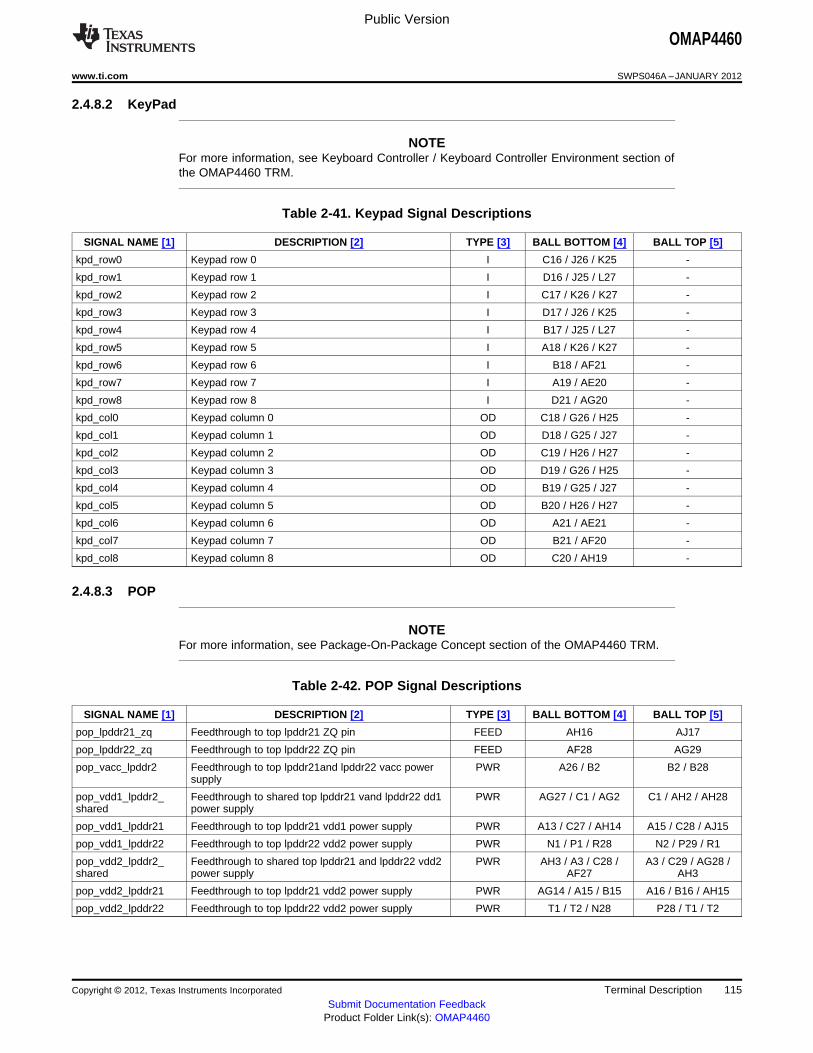
Public Version
OMAP4460
www.ti.com SWPS046A –JANUARY 2012
2.4.8.2 KeyPad
NOTEFor more information, see Keyboard Controller / Keyboard Controller Environment section ofthe OMAP4460 TRM.
Table 2-41. Keypad Signal Descriptions
SIGNAL NAME [1] DESCRIPTION [2] TYPE [3] BALL BOTTOM [4] BALL TOP [5]
kpd_row0 Keypad row 0 I C16 / J26 / K25 -
kpd_row1 Keypad row 1 I D16 / J25 / L27 -
kpd_row2 Keypad row 2 I C17 / K26 / K27 -
kpd_row3 Keypad row 3 I D17 / J26 / K25 -
kpd_row4 Keypad row 4 I B17 / J25 / L27 -
kpd_row5 Keypad row 5 I A18 / K26 / K27 -
kpd_row6 Keypad row 6 I B18 / AF21 -
kpd_row7 Keypad row 7 I A19 / AE20 -
kpd_row8 Keypad row 8 I D21 / AG20 -
kpd_col0 Keypad column 0 OD C18 / G26 / H25 -
kpd_col1 Keypad column 1 OD D18 / G25 / J27 -
kpd_col2 Keypad column 2 OD C19 / H26 / H27 -
kpd_col3 Keypad column 3 OD D19 / G26 / H25 -
kpd_col4 Keypad column 4 OD B19 / G25 / J27 -
kpd_col5 Keypad column 5 OD B20 / H26 / H27 -
kpd_col6 Keypad column 6 OD A21 / AE21 -
kpd_col7 Keypad column 7 OD B21 / AF20 -
kpd_col8 Keypad column 8 OD C20 / AH19 -
2.4.8.3 POP
NOTEFor more information, see Package-On-Package Concept section of the OMAP4460 TRM.
Table 2-42. POP Signal Descriptions
SIGNAL NAME [1] DESCRIPTION [2] TYPE [3] BALL BOTTOM [4] BALL TOP [5]
pop_lpddr21_zq Feedthrough to top lpddr21 ZQ pin FEED AH16 AJ17
pop_lpddr22_zq Feedthrough to top lpddr22 ZQ pin FEED AF28 AG29
pop_vacc_lpddr2 Feedthrough to top lpddr21and lpddr22 vacc power PWR A26 / B2 B2 / B28supply
pop_vdd1_lpddr2_ Feedthrough to shared top lpddr21 vand lpddr22 dd1 PWR AG27 / C1 / AG2 C1 / AH2 / AH28shared power supply
pop_vdd1_lpddr21 Feedthrough to top lpddr21 vdd1 power supply PWR A13 / C27 / AH14 A15 / C28 / AJ15
pop_vdd1_lpddr22 Feedthrough to top lpddr22 vdd2 power supply PWR N1 / P1 / R28 N2 / P29 / R1
pop_vdd2_lpddr2_ Feedthrough to shared top lpddr21 and lpddr22 vdd2 PWR AH3 / A3 / C28 / A3 / C29 / AG28 /shared power supply AF27 AH3
pop_vdd2_lpddr21 Feedthrough to top lpddr21 vdd2 power supply PWR AG14 / A15 / B15 A16 / B16 / AH15
pop_vdd2_lpddr22 Feedthrough to top lpddr22 vdd2 power supply PWR T1 / T2 / N28 P28 / T1 / T2
Copyright © 2012, Texas Instruments Incorporated Terminal Description 115Submit Documentation Feedback
Product Folder Link(s): OMAP4460
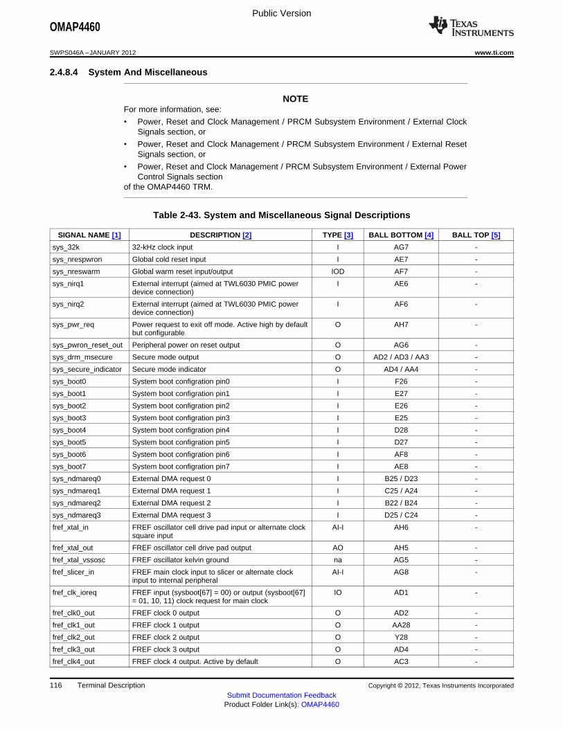
Public Version
OMAP4460
SWPS046A –JANUARY 2012 www.ti.com
2.4.8.4 System And Miscellaneous
NOTEFor more information, see:
• Power, Reset and Clock Management / PRCM Subsystem Environment / External ClockSignals section, or
• Power, Reset and Clock Management / PRCM Subsystem Environment / External ResetSignals section, or
• Power, Reset and Clock Management / PRCM Subsystem Environment / External PowerControl Signals section
of the OMAP4460 TRM.
Table 2-43. System and Miscellaneous Signal Descriptions
SIGNAL NAME [1] DESCRIPTION [2] TYPE [3] BALL BOTTOM [4] BALL TOP [5]
sys_32k 32-kHz clock input I AG7 -
sys_nrespwron Global cold reset input I AE7 -
sys_nreswarm Global warm reset input/output IOD AF7 -
sys_nirq1 External interrupt (aimed at TWL6030 PMIC power I AE6 -device connection)
sys_nirq2 External interrupt (aimed at TWL6030 PMIC power I AF6 -device connection)
sys_pwr_req Power request to exit off mode. Active high by default O AH7 -but configurable
sys_pwron_reset_out Peripheral power on reset output O AG6 -
sys_drm_msecure Secure mode output O AD2 / AD3 / AA3 -
sys_secure_indicator Secure mode indicator O AD4 / AA4 -
sys_boot0 System boot configration pin0 I F26 -
sys_boot1 System boot configration pin1 I E27 -
sys_boot2 System boot configration pin2 I E26 -
sys_boot3 System boot configration pin3 I E25 -
sys_boot4 System boot configration pin4 I D28 -
sys_boot5 System boot configration pin5 I D27 -
sys_boot6 System boot configration pin6 I AF8 -
sys_boot7 System boot configration pin7 I AE8 -
sys_ndmareq0 External DMA request 0 I B25 / D23 -
sys_ndmareq1 External DMA request 1 I C25 / A24 -
sys_ndmareq2 External DMA request 2 I B22 / B24 -
sys_ndmareq3 External DMA request 3 I D25 / C24 -
fref_xtal_in FREF oscillator cell drive pad input or alternate clock AI-I AH6 -square input
fref_xtal_out FREF oscillator cell drive pad output AO AH5 -
fref_xtal_vssosc FREF oscillator kelvin ground na AG5 -
fref_slicer_in FREF main clock input to slicer or alternate clock AI-I AG8 -input to internal peripheral
fref_clk_ioreq FREF input (sysboot[67] = 00) or output (sysboot[67] IO AD1 -= 01, 10, 11) clock request for main clock
fref_clk0_out FREF clock 0 output O AD2 -
fref_clk1_out FREF clock 1 output O AA28 -
fref_clk2_out FREF clock 2 output O Y28 -
fref_clk3_out FREF clock 3 output O AD4 -
fref_clk4_out FREF clock 4 output. Active by default O AC3 -
116 Terminal Description Copyright © 2012, Texas Instruments Incorporated
Submit Documentation FeedbackProduct Folder Link(s): OMAP4460
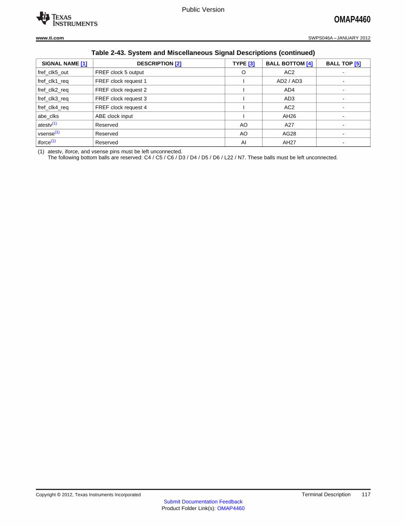
Public Version
OMAP4460
www.ti.com SWPS046A –JANUARY 2012
Table 2-43. System and Miscellaneous Signal Descriptions (continued)
SIGNAL NAME [1] DESCRIPTION [2] TYPE [3] BALL BOTTOM [4] BALL TOP [5]
fref_clk5_out FREF clock 5 output O AC2 -
fref_clk1_req FREF clock request 1 I AD2 / AD3 -
fref_clk2_req FREF clock request 2 I AD4 -
fref_clk3_req FREF clock request 3 I AD3 -
fref_clk4_req FREF clock request 4 I AC2 -
abe_clks ABE clock input I AH26 -
atestv(1) Reserved AO A27 -
vsense(1) Reserved AO AG28 -
iforce(1) Reserved AI AH27 -
(1) atestv, iforce, and vsense pins must be left unconnected.The following bottom balls are reserved: C4 / C5 / C6 / D3 / D4 / D5 / D6 / L22 / N7. These balls must be left unconnected.
Copyright © 2012, Texas Instruments Incorporated Terminal Description 117Submit Documentation Feedback
Product Folder Link(s): OMAP4460
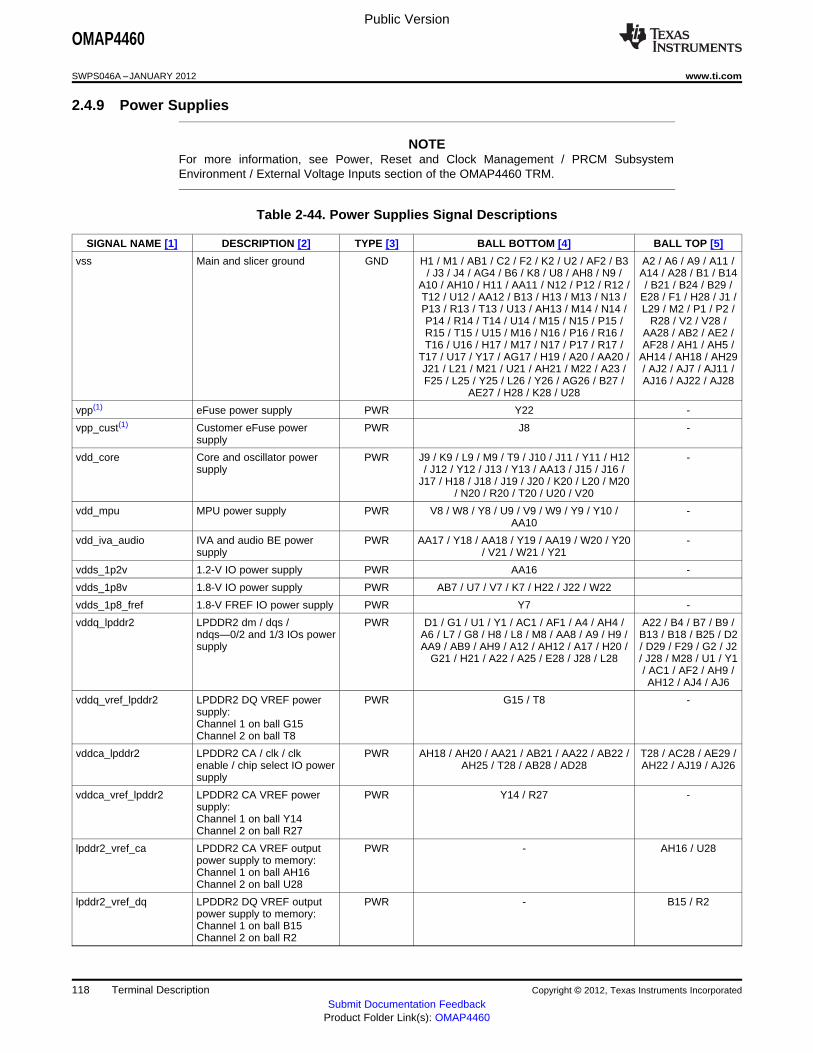
Public Version
OMAP4460
SWPS046A –JANUARY 2012 www.ti.com
2.4.9 Power Supplies
NOTEFor more information, see Power, Reset and Clock Management / PRCM SubsystemEnvironment / External Voltage Inputs section of the OMAP4460 TRM.
Table 2-44. Power Supplies Signal Descriptions
SIGNAL NAME [1] DESCRIPTION [2] TYPE [3] BALL BOTTOM [4] BALL TOP [5]
vss Main and slicer ground GND H1 / M1 / AB1 / C2 / F2 / K2 / U2 / AF2 / B3 A2 / A6 / A9 / A11 // J3 / J4 / AG4 / B6 / K8 / U8 / AH8 / N9 / A14 / A28 / B1 / B14
A10 / AH10 / H11 / AA11 / N12 / P12 / R12 / / B21 / B24 / B29 /T12 / U12 / AA12 / B13 / H13 / M13 / N13 / E28 / F1 / H28 / J1 /P13 / R13 / T13 / U13 / AH13 / M14 / N14 / L29 / M2 / P1 / P2 /P14 / R14 / T14 / U14 / M15 / N15 / P15 / R28 / V2 / V28 /R15 / T15 / U15 / M16 / N16 / P16 / R16 / AA28 / AB2 / AE2 /T16 / U16 / H17 / M17 / N17 / P17 / R17 / AF28 / AH1 / AH5 /
T17 / U17 / Y17 / AG17 / H19 / A20 / AA20 / AH14 / AH18 / AH29J21 / L21 / M21 / U21 / AH21 / M22 / A23 / / AJ2 / AJ7 / AJ11 /F25 / L25 / Y25 / L26 / Y26 / AG26 / B27 / AJ16 / AJ22 / AJ28
AE27 / H28 / K28 / U28
vpp(1) eFuse power supply PWR Y22 -
vpp_cust(1) Customer eFuse power PWR J8 -supply
vdd_core Core and oscillator power PWR J9 / K9 / L9 / M9 / T9 / J10 / J11 / Y11 / H12 -supply / J12 / Y12 / J13 / Y13 / AA13 / J15 / J16 /
J17 / H18 / J18 / J19 / J20 / K20 / L20 / M20/ N20 / R20 / T20 / U20 / V20
vdd_mpu MPU power supply PWR V8 / W8 / Y8 / U9 / V9 / W9 / Y9 / Y10 / -AA10
vdd_iva_audio IVA and audio BE power PWR AA17 / Y18 / AA18 / Y19 / AA19 / W20 / Y20 -supply / V21 / W21 / Y21
vdds_1p2v 1.2-V IO power supply PWR AA16 -
vdds_1p8v 1.8-V IO power supply PWR AB7 / U7 / V7 / K7 / H22 / J22 / W22
vdds_1p8_fref 1.8-V FREF IO power supply PWR Y7 -
vddq_lpddr2 LPDDR2 dm / dqs / PWR D1 / G1 / U1 / Y1 / AC1 / AF1 / A4 / AH4 / A22 / B4 / B7 / B9 /ndqs—0/2 and 1/3 IOs power A6 / L7 / G8 / H8 / L8 / M8 / AA8 / A9 / H9 / B13 / B18 / B25 / D2supply AA9 / AB9 / AH9 / A12 / AH12 / A17 / H20 / / D29 / F29 / G2 / J2
G21 / H21 / A22 / A25 / E28 / J28 / L28 / J28 / M28 / U1 / Y1/ AC1 / AF2 / AH9 /AH12 / AJ4 / AJ6
vddq_vref_lpddr2 LPDDR2 DQ VREF power PWR G15 / T8 -supply:Channel 1 on ball G15Channel 2 on ball T8
vddca_lpddr2 LPDDR2 CA / clk / clk PWR AH18 / AH20 / AA21 / AB21 / AA22 / AB22 / T28 / AC28 / AE29 /enable / chip select IO power AH25 / T28 / AB28 / AD28 AH22 / AJ19 / AJ26supply
vddca_vref_lpddr2 LPDDR2 CA VREF power PWR Y14 / R27 -supply:Channel 1 on ball Y14Channel 2 on ball R27
lpddr2_vref_ca LPDDR2 CA VREF output PWR - AH16 / U28power supply to memory:Channel 1 on ball AH16Channel 2 on ball U28
lpddr2_vref_dq LPDDR2 DQ VREF output PWR - B15 / R2power supply to memory:Channel 1 on ball B15Channel 2 on ball R2
118 Terminal Description Copyright © 2012, Texas Instruments Incorporated
Submit Documentation FeedbackProduct Folder Link(s): OMAP4460

Public Version
OMAP4460
www.ti.com SWPS046A –JANUARY 2012
Table 2-44. Power Supplies Signal Descriptions (continued)
SIGNAL NAME [1] DESCRIPTION [2] TYPE [3] BALL BOTTOM [4] BALL TOP [5]
vdda_dll0_lpddr21 LPDDR21 DLL power supply PWR G22 -providing clocks to byte 0and 2
vdda_dll1_lpddr21 LPDDR21 DLL power supply PWR G9 -providing clocks to byte 1and 3
vdda_dll0_lpddr22 LPDDR22 DLL power supply PWR M7 -providing clocks to byte 0and 2
vdda_dll1_lpddr22 LPDDR22 DLL power supply PWR AB10 -providing clocks to byte 1and 3
vdda_dsi1 DSI1 PHY power supply PWR L1 -
vssa_dsi DSI1 and DSI2 PHY ground GND N8 / P8 -
vdda_dsi2 DSI2 PHY power supply PWR L2 -
vdda_csi21 CSI21 PHY power supply PWR W28 -
vssa_csi2 CSI21 and CSI22 PHY GND R22 -ground
vdda_csi22 CSI22 PHY power supply PWR V28 -
vdda_hdmi_vdac HDMI PHY PHY power PWR A11 / G12 -supply
vssa_hdmi_vdac HDMI PHY ground GND G11 -
vdda_usba0otg_3p3v USB PHY 3.3-V power PWR A5 -supply
vssa_usba0otg_3p3v USB PHY 3.3-V ground GND G10 -
vdda_usba0otg_1p8v USB PHY 1.8-V power PWR A7 -supply
vssa_usba0otg USB PHY 1.8-V ground GND H10 -
vdds_usim SIM dual voltage IO power PWR J7 -supply
pbias_sim SIM pbias output PWR A2
vdds_sdmmc1 SDMMC1 dual voltage IO PWR G7 / H7 -power supply
pbias_mmc1 SDMMC1 pbias output PWR A1
vdda_dpll_mpu MPU DPLL power supply PWR P9 -
vdda_dpll_core_audio Core and audio DPLLs PWR G13 -power supply
vdda_dpll_iva_per Peripheral and IVA DPLL PWR Y16 -power supply
vdds_dv_gpmc GPMC dual voltage IO power PWR G20 -supply
vdds_dv_sdmmc2 SDMMC2 dual voltage IO PWR G16 / H16 -power supply
vdds_dv_c2c GPMC second dual voltage PWR G17 / G18 / G19 -IO power supply
vdds_dv_cam Camera dual voltage IO PWR V22 -power supply
vdds_dv_bank0 Serial bank0 dual voltage IO PWR AB16 -power supply
vdds_dv_bank1 Serial bank1 dual voltage IO PWR AB20 -power supply
vdds_dv_bank2 Serial bank2 dual voltage IO PWR AB8 / AB19 -power supply
vdds_dv_bank3 Serial bank3 dual voltage IO PWR AB18 -power supply
Copyright © 2012, Texas Instruments Incorporated Terminal Description 119Submit Documentation Feedback
Product Folder Link(s): OMAP4460
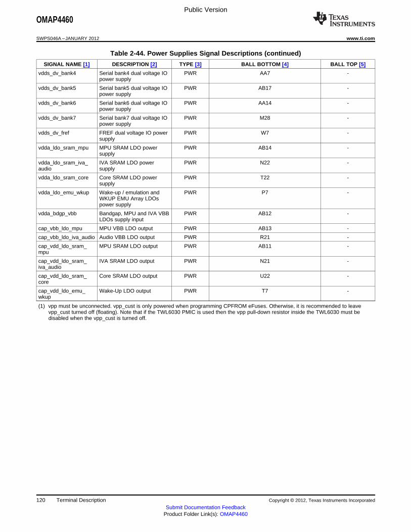
Public Version
OMAP4460
SWPS046A –JANUARY 2012 www.ti.com
Table 2-44. Power Supplies Signal Descriptions (continued)
SIGNAL NAME [1] DESCRIPTION [2] TYPE [3] BALL BOTTOM [4] BALL TOP [5]
vdds_dv_bank4 Serial bank4 dual voltage IO PWR AA7 -power supply
vdds_dv_bank5 Serial bank5 dual voltage IO PWR AB17 -power supply
vdds_dv_bank6 Serial bank6 dual voltage IO PWR AA14 -power supply
vdds_dv_bank7 Serial bank7 dual voltage IO PWR M28 -power supply
vdds_dv_fref FREF dual voltage IO power PWR W7 -supply
vdda_ldo_sram_mpu MPU SRAM LDO power PWR AB14 -supply
vdda_ldo_sram_iva_ IVA SRAM LDO power PWR N22 -audio supply
vdda_ldo_sram_core Core SRAM LDO power PWR T22 -supply
vdda_ldo_emu_wkup Wake-up / emulation and PWR P7 -WKUP EMU Array LDOspower supply
vdda_bdgp_vbb Bandgap, MPU and IVA VBB PWR AB12 -LDOs supply input
cap_vbb_ldo_mpu MPU VBB LDO output PWR AB13 -
cap_vbb_ldo_iva_audio Audio VBB LDO output PWR R21 -
cap_vdd_ldo_sram_ MPU SRAM LDO output PWR AB11 -mpu
cap_vdd_ldo_sram_ IVA SRAM LDO output PWR N21 -iva_audio
cap_vdd_ldo_sram_ Core SRAM LDO output PWR U22 -core
cap_vdd_ldo_emu_ Wake-Up LDO output PWR T7 -wkup
(1) vpp must be unconnected. vpp_cust is only powered when programming CPFROM eFuses. Otherwise, it is recommended to leavevpp_cust turned off (floating). Note that if the TWL6030 PMIC is used then the vpp pull-down resistor inside the TWL6030 must bedisabled when the vpp_cust is turned off.
120 Terminal Description Copyright © 2012, Texas Instruments Incorporated
Submit Documentation FeedbackProduct Folder Link(s): OMAP4460
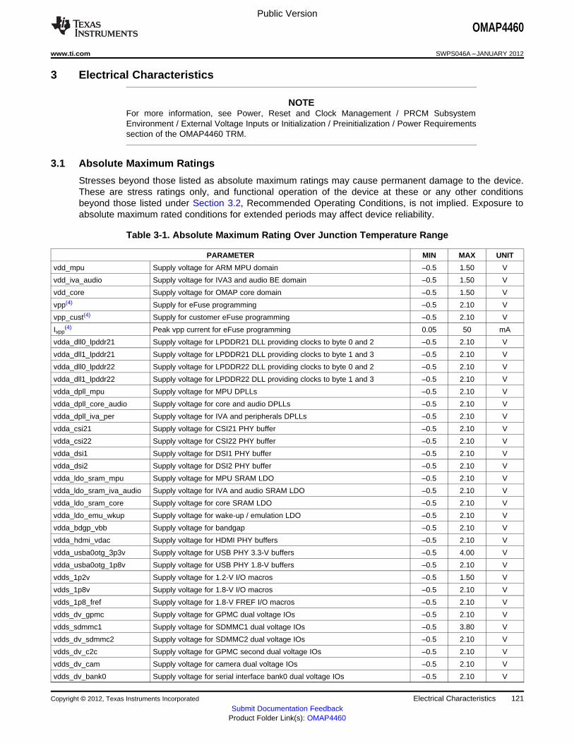
Public Version
OMAP4460
www.ti.com SWPS046A –JANUARY 2012
3 Electrical Characteristics
NOTEFor more information, see Power, Reset and Clock Management / PRCM SubsystemEnvironment / External Voltage Inputs or Initialization / Preinitialization / Power Requirementssection of the OMAP4460 TRM.
3.1 Absolute Maximum Ratings
Stresses beyond those listed as absolute maximum ratings may cause permanent damage to the device.These are stress ratings only, and functional operation of the device at these or any other conditionsbeyond those listed under Section 3.2, Recommended Operating Conditions, is not implied. Exposure toabsolute maximum rated conditions for extended periods may affect device reliability.
Table 3-1. Absolute Maximum Rating Over Junction Temperature Range
PARAMETER MIN MAX UNIT
vdd_mpu Supply voltage for ARM MPU domain –0.5 1.50 V
vdd_iva_audio Supply voltage for IVA3 and audio BE domain –0.5 1.50 V
vdd_core Supply voltage for OMAP core domain –0.5 1.50 V
vpp(4) Supply for eFuse programming –0.5 2.10 V
vpp_cust(4) Supply for customer eFuse programming –0.5 2.10 V
Ivpp(4) Peak vpp current for eFuse programming 0.05 50 mA
vdda_dll0_lpddr21 Supply voltage for LPDDR21 DLL providing clocks to byte 0 and 2 –0.5 2.10 V
vdda_dll1_lpddr21 Supply voltage for LPDDR21 DLL providing clocks to byte 1 and 3 –0.5 2.10 V
vdda_dll0_lpddr22 Supply voltage for LPDDR22 DLL providing clocks to byte 0 and 2 –0.5 2.10 V
vdda_dll1_lpddr22 Supply voltage for LPDDR22 DLL providing clocks to byte 1 and 3 –0.5 2.10 V
vdda_dpll_mpu Supply voltage for MPU DPLLs –0.5 2.10 V
vdda_dpll_core_audio Supply voltage for core and audio DPLLs –0.5 2.10 V
vdda_dpll_iva_per Supply voltage for IVA and peripherals DPLLs –0.5 2.10 V
vdda_csi21 Supply voltage for CSI21 PHY buffer –0.5 2.10 V
vdda_csi22 Supply voltage for CSI22 PHY buffer –0.5 2.10 V
vdda_dsi1 Supply voltage for DSI1 PHY buffer –0.5 2.10 V
vdda_dsi2 Supply voltage for DSI2 PHY buffer –0.5 2.10 V
vdda_ldo_sram_mpu Supply voltage for MPU SRAM LDO –0.5 2.10 V
vdda_ldo_sram_iva_audio Supply voltage for IVA and audio SRAM LDO –0.5 2.10 V
vdda_ldo_sram_core Supply voltage for core SRAM LDO –0.5 2.10 V
vdda_ldo_emu_wkup Supply voltage for wake-up / emulation LDO –0.5 2.10 V
vdda_bdgp_vbb Supply voltage for bandgap –0.5 2.10 V
vdda_hdmi_vdac Supply voltage for HDMI PHY buffers –0.5 2.10 V
vdda_usba0otg_3p3v Supply voltage for USB PHY 3.3-V buffers –0.5 4.00 V
vdda_usba0otg_1p8v Supply voltage for USB PHY 1.8-V buffers –0.5 2.10 V
vdds_1p2v Supply voltage for 1.2-V I/O macros –0.5 1.50 V
vdds_1p8v Supply voltage for 1.8-V I/O macros –0.5 2.10 V
vdds_1p8_fref Supply voltage for 1.8-V FREF I/O macros –0.5 2.10 V
vdds_dv_gpmc Supply voltage for GPMC dual voltage IOs –0.5 2.10 V
vdds_sdmmc1 Supply voltage for SDMMC1 dual voltage IOs –0.5 3.80 V
vdds_dv_sdmmc2 Supply voltage for SDMMC2 dual voltage IOs –0.5 2.10 V
vdds_dv_c2c Supply voltage for GPMC second dual voltage IOs –0.5 2.10 V
vdds_dv_cam Supply voltage for camera dual voltage IOs –0.5 2.10 V
vdds_dv_bank0 Supply voltage for serial interface bank0 dual voltage IOs –0.5 2.10 V
Copyright © 2012, Texas Instruments Incorporated Electrical Characteristics 121Submit Documentation Feedback
Product Folder Link(s): OMAP4460

Public Version
OMAP4460
SWPS046A –JANUARY 2012 www.ti.com
Table 3-1. Absolute Maximum Rating Over Junction Temperature Range (continued)
PARAMETER MIN MAX UNIT
vdds_dv_bank1 Supply voltage for serial interface bank1 dual voltage IOs –0.5 2.10 V
vdds_dv_bank2 Supply voltage for serial interface bank2 dual voltage IOs –0.5 2.10 V
vdds_dv_bank3 Supply voltage for serial interface bank3 dual voltage IOs –0.5 2.10 V
vdds_dv_bank4 Supply voltage for serial interface bank4 dual voltage IOs –0.5 2.10 V
vdds_dv_bank5 Supply voltage for serial interface bank5 dual voltage IOs –0.5 2.10 V
vdds_dv_bank6 Supply voltage for serial interface bank6 dual voltage IOs –0.5 2.10 V
vdds_dv_bank7 Supply voltage for serial interface bank7 dual voltage IOs –0.5 2.10 V
vdds_dv_fref Supply voltage for FREF dual voltage IOs –0.5 2.10 V
vdds_usim Supply voltage for SIM dual voltage IOs –0.5 3.80 V
vddq_lpddr2 Supply voltage for LPDDR2 IOs –0.4 1.50 V
vddq_vref_lpddr2 Supply voltage for LPDDR2 DQ VREF: –0.4 1.50 VChannel 1 on ball G15Channel 2 on ball T8
vddca_lpddr2 Supply voltage for LPDDR2 CA, clock, clock enable, and chip select IOs –0.4 1.50 V
vddca_vref_lpddr2 Supply voltage for LPDDR2 CA VREF: –0.4 1.50 VChannel 1 on ball Y14Channel 2 on ball R27
VESD ESD stress voltage(1) HBM (Human Body Model)(2) >1000 V
CDM (Charged Device Model)(3) >250
IIOI Current-pulse injection on each I/O pin(6) 100(7) mA
Iclamp Clamp current for an input or output –20 20 mA
TSTG(5) Storage temperature range after soldered onto PC Board –65 150 °C
(1) Electrostatic discharge (ESD) to measure device sensitivity/immunity to damage caused by electrostatic discharges into the device.
(2) Level listed is the passing level per ANSI/ESDA/JEDEC JS-001. JEDEC document JEP155 states that 500-V HBM allows safemanufacturing with a standard ESD control process, and manufacturing with less than 500-V HBM is possible if necessary precautionsare taken. Pins listed as 1000V may actually have higher performance.
(3) Level listed is the passing level per EIA-JEDEC JESD22-C101E. JEDEC document JEP157 states that 250-V CDM allows safemanufacturing with a standard ESD control process, and manufacturing with less than 250-V CDM is possible if necessary precautionsare taken. Pins listed as 250 V may actually have higher performance.
(4) vpp must be unconnected. vpp_cust is only powered when programming CPFROM eFuses. Otherwise, it is recommended to leavevpp_cust turned off (floating). Note that if the TWL6030 PMIC is used then the vpp pull-down resistor inside the TWL6030 must bedisabled when the vpp_cust is turned off.
(5) For tape and reel the storage temperature range is [–10°C to 50°C] with a maximum relative humidity of 70%. It is recommendedreturning to ambient room temperature before usage.
(6) Latch-up testing per JEDEC JESD78 stressed with I/O pin injection of the lower of specified current or the current reached at 1.5 timesmaximum I/O voltage.
(7) sdmmc1_clk (Ball D2) passes 95-mA current injection at room temperature.sdmmc1_clk (Ball D2), sdmmc1_dat2 (Ball E1) passes 45-mA at 105°C and sdmmc1_dat1 (Ball E2) passes 65-mA at 105°C.
Table 3-2 summarizes the power consumption at the ball level.
Table 3-2. Maximum Current Ratings at Ball Level
PARAMETER MAX UNIT
SIGNAL DESCRIPTION
vdd_mpu(1) Maximum current rating for ARM MPU OPPNTSB (MPU @ 1500 MHz) 2300 mA
OPPNT (MPU @ 1200 MHz) 1800
vdd_iva_audio(1) Maximum current rating for IVA3 and audio BE (including in OPPNTSB mode) 1000 mA
vdd_core(1) Maximum current rating for OMAP Core (including in overdrive mode – OPP119%) 1200 mA
vpp(4) Maximum current rating for eFuse programming 50 mA
vpp_cust(4) Maximum current rating for customer eFuse programming 50 mA
vdda_dll0_lpddr21 Maximum current rating for LPDDR21 DLL providing clocks to bytes 0 and 2 5 mA
vdda_dll1_lpddr21 Maximum current rating for LPDDR21 DLL providing clocks to bytes 1 and 3 5 mA
122 Electrical Characteristics Copyright © 2012, Texas Instruments Incorporated
Submit Documentation FeedbackProduct Folder Link(s): OMAP4460

Public Version
OMAP4460
www.ti.com SWPS046A –JANUARY 2012
Table 3-2. Maximum Current Ratings at Ball Level (continued)
PARAMETER MAX UNIT
SIGNAL DESCRIPTION
vdda_dll0_lpddr22 Maximum current rating for LPDDR22 DLL providing clocks to bytes 0 and 2 5 mA
vdda_dll1_lpddr22 Maximum current rating for LPDDR22 DLL providing clocks to bytes 1 and 3 5 mA
vdda_dpll_mpu Maximum current rating for MPU DPLLs 5 mA
vdda_dpll_core_audio Maximum current rating for core and audio DPLLs 10 mA
vdda_dpll_iva_per Maximum current rating for IVA and peripheral DPLLs 10 mA
vdda_csi21 Maximum current rating for CSI21 PHY buffer 10 mA
vdda_csi22 Maximum current rating for CSI22 PHY buffer 5 mA
vdda_dsi1 Maximum current rating for DSI1 PHY buffer 15 mA
vdda_dsi2 Maximum current rating for DSI2 PHY buffer 10 mA
vdda_ldo_sram_mpu Maximum current rating for MPU SRAM LDO 30 mA
vdda_ldo_sram_iva_audio Maximum current rating for IVA and audio SRAM LDO 30 mA
vdda_ldo_sram_core Maximum current rating for Core SRAM LDO 30 mA
vdda_ldo_emu_wkup Maximum current rating for wake-up / emulation LDO 60 mA
vdda_bdgp_vbb Maximum current rating for bandgap 60 mA
vdda_hdmi_vdac Maximum current rating for HDMI PHY buffers 35 mA
vdda_usba0otg_3p3v Maximum current rating for USB PHY 3.3-V buffers 30 mA
vdda_usba0otg_1p8v Maximum current rating for USB PHY 1.8-V buffers 35 mA
vdds_1p2v Maximum current rating for 1.2-V I/O macros 20 mA
vdds_1p8v Maximum current rating for 1.8-V I/O macros 140 mA
vdds_1p8_fref Maximum current rating for 1.8-V FREF I/O macros 5 mA
vdds_dv_gpmc Maximum current rating for GPMC dual voltage IOs 10 mA
vdds_sdmmc1(2) Maximum current rating for SDMMC1 dual voltage IOs 20 mA
vdds_dv_sdmmc2(2) Maximum current rating for SDMMC2 dual voltage IOs 10 mA
vdds_dv_c2c Maximum current rating for GPMC second dual voltage IOs 5 mA
vdds_dv_cam Maximum current rating for Camera dual voltage IOs 5 mA
vdds_dv_bank0 Maximum current rating for serial interface bank0 dual voltage IOs 5 mA
vdds_dv_bank1 Maximum current rating for serial interface bank1 dual voltage IOs 5 mA
vdds_dv_bank2 Maximum current rating for serial interface bank2 dual voltage IOs 5 mA
vdds_dv_bank3 Maximum current rating for serial interface bank3 dual voltage IOs 5 mA
vdds_dv_bank4 Maximum current rating for serial interface bank4 dual voltage IOs 5 mA
vdds_dv_bank5 Maximum current rating for serial interface bank5 dual voltage IOs 5 mA
vdds_dv_bank6 Maximum current rating for serial interface bank6 dual voltage IOs 5 mA
vdds_dv_bank7 Maximum current rating for serial interface bank6 dual voltage IOs 5 mA
vdds_dv_fref Maximum current rating for FREF dual voltage IOs 5 mA
vdds_usim(3) Maximum current rating for SIM dual voltage IOs 20 mA
vddq_lpddr2 Maximum current rating for LPDDR2 IOs 275 mA
vddq_vref_lpddr2 Maximum current rating for LPDDR2 DQ VREF: 1 mAChannel 1 on ball G15Channel 2 on ball T8
vddca_lpddr2 Maximum current rating for LPDDR2 CA, clock, clock enable and chip select IOs 25 mA
vddca_vref_lpddr2 Maximum current rating for LPDDR2 CA VREF: 1 mAChannel 1 on ball Y14Channel 2 on ball R27
(1) With SmartReflex™ enabled.
(2) MMC card and I/O card are not included.
(3) SIM card and I/O card are not included.
(4) vpp must be unconnected. vpp_cust is only powered when programming CPFROM eFuses. Otherwise, it is recommended to leavevpp_cust turned off (floating). Note that if the TWL6030 PMIC is used then the vpp pull-down resistor inside the TWL6030 must be
Copyright © 2012, Texas Instruments Incorporated Electrical Characteristics 123Submit Documentation Feedback
Product Folder Link(s): OMAP4460
Public Version
OMAP4460
SWPS046A –JANUARY 2012 www.ti.com
disabled when the vpp_cust is turned off.
124 Electrical Characteristics Copyright © 2012, Texas Instruments Incorporated
Submit Documentation FeedbackProduct Folder Link(s): OMAP4460
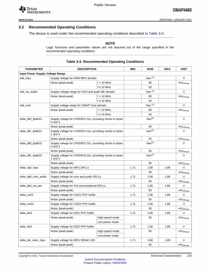
Public Version
OMAP4460
www.ti.com SWPS046A –JANUARY 2012
3.2 Recommended Operating Conditions
The device is used under the recommended operating conditions described in Table 3-3.
NOTELogic functions and parameter values are not assured out of the range specified in therecommended operating conditions.
Table 3-3. Recommended Operating Conditions
PARAMETER DESCRIPTION MIN NOM MAX UNIT
Input Power Supply Voltage Range
vdd_mpu Supply voltage for ARM MPU domain See (1) V
Noise (peak-peak) f < 10 MHz 80 mVPPmax
f ≥ 10 MHz 50
vdd_iva_audio Supply voltage range for IVA3 and audio BE domain See (1) V
Noise (peak-peak) f < 10 MHz 80 mVPPmax
f ≥ 10 MHz 50
vdd_core Supply voltage range for OMAP Core domain See (1) V
Noise (peak-peak) f < 10 MHz 80 mVPPmax
f ≥ 10 MHz 50
vdda_dll0_lpddr21 Supply voltage for LPDDR21 DLL providing clocks to bytes See(4) V0 and 2
Noise (peak-peak) 50 mVPPmax
vdda_dll1_lpddr21 Supply voltage for LPDDR21 DLL providing clocks to bytes See(4) V1 and 3
Noise (peak-peak) 50 mVPPmax
vdda_dll0_lpddr22 Supply voltage for LPDDR22 DLL providing clocks to bytes See(4) V0 and 2
Noise (peak-peak) 50 mVPPmax
vdda_dll1_lpddr22 Supply voltage for LPDDR22 DLL providing clocks to bytes See(4) V1 and 3
Noise (peak-peak) 50 mVPPmax
vdda_dpll_mpu Supply voltage for MPU DPLLs 1.71 1.80 1.89 V
Noise (peak-peak) 50 mVPPmax
vdda_dpll_core_audio Supply voltage for core and audio DPLLs 1.71 1.80 1.89 V
Noise (peak-peak) 50 mVPPmax
vdda_dpll_iva_per Supply voltage for IVA and peripheral DPLLs 1.71 1.80 1.89 V
Noise (peak-peak) 50 mVPPmax
vdda_csi21 Supply voltage for CSI21 PHY buffer 1.71 1.80 1.89 V
Noise (peak-peak) 50 mVPPmax
vdda_csi22 Supply voltage for CSI22 PHY buffer 1.71 1.80 1.89 V
Noise (peak-peak) 50 mVPPmax
vdda_dsi1 Supply voltage for DSI1 PHY buffer 1.71 1.80 1.89 V
Noise (peak-peak) High-speed mode 50 mVPPmax
Low-power mode
vdda_dsi2 Supply voltage for DSI2 PHY buffer 1.71 1.80 1.89 V
Noise (peak-peak) High-speed mode 50 mVPPmax
Low-power mode
vdda_ldo_sram_mpu Supply voltage for MPU SRAM LDO 1.71 1.80 1.89 V
Noise (peak-peak) 50 mVPPmax
Copyright © 2012, Texas Instruments Incorporated Electrical Characteristics 125Submit Documentation Feedback
Product Folder Link(s): OMAP4460

Public Version
OMAP4460
SWPS046A –JANUARY 2012 www.ti.com
Table 3-3. Recommended Operating Conditions (continued)
PARAMETER DESCRIPTION MIN NOM MAX UNIT
vdda_ldo_sram_iva_ Supply voltage for IVA and audio SRAM LDO 1.71 1.80 1.89 Vaudio Noise (peak-peak) 50 mVPPmax
vdda_ldo_sram_core Supply voltage for Core SRAM LDO 1.71 1.80 1.89 V
Noise (peak-peak) 50 mVPPmax
vdda_ldo_emu_wkup Supply voltage for wake-up / emulation LDO 1.00 1.20 1.26 V
Noise (peak-peak) 50 mVPPmax
vdda_bdgp_vbb Supply voltage for bandgap 1.71 1.80 1.89 V
Noise (peak-peak) 50 mVPPmax
vdda_hdmi_vdac Supply voltage for HDMI PHY buffers 1.71 1.80 1.89 V
Noise (peak-peak) 50 mVPPmax
vdda_usba0otg_3p3v Supply voltage for USB PHY 3.3-V buffers 3.0 3.3 3.6 V
Noise (peak-peak) 50 mVPPmax
vdda_usba0otg_1p8v Supply voltage for USB PHY 1.8-V buffers 1.71 1.80 1.89 V
Noise (peak-peak) 50 mVPPmax
vdds_1p2v Supply voltage for 1.2-V I/O macros 1.14 1.20 1.26 V
Noise (peak-peak) 50 mVPPmax
vdds_1p8v Supply voltage for 1.8-V I/O macros 1.71 1.80 1.89 V
Noise (peak-peak) 50 mVPPmax
vdds_1p8_fref Supply voltage for 1.8-V FREF I/O macros 1.71 1.80 1.89 V
Noise (peak-peak) 50 mVPPmax
vdds_dv_gpmc Supply voltage for GPMC dual 1.2-V Mode 1.14 1.20 1.26 Vvoltage IOs 1.8-V Mode 1.71 1.80 1.89
Noise (peak-peak) 1.2-V Mode 50 mVPPmax
1.8-V Mode
vdds_sdmmc1(2) Supply voltage for SDMMC1 dual 1.8-V Mode 1.71 1.80 1.89 Vvoltage IOs 3.0-V Mode 2.7 3.0 3.6
Noise (peak-peak) 1.8-V Mode 50 mVPPmax
3.0-V Mode
vdds_dv_sdmmc2(2) Supply voltage for SDMMC2 dual 1.2-V Mode 1.14 1.20 1.26 Vvoltage IOs 1.8-V Mode 1.71 1.80 1.89
Noise (peak-peak) 1.2-V Mode 50 mVPPmax
1.8-V Mode
vdds_dv_c2c Supply voltage for GPMC second 1.2-V Mode 1.14 1.20 1.26 Vdual voltage IOs 1.8-V Mode 1.71 1.80 1.89
Noise (peak-peak) 1.2-V Mode 50 mVPPmax
1.8-V Mode
vdds_dv_cam Supply voltage for Camera dual 1.2-V Mode 1.14 1.20 1.26 Vvoltage IOs 1.8-V Mode 1.71 1.80 1.89
Noise (peak-peak) 1.2-V Mode 50 mVPPmax
1.8-V Mode
vdds_dv_bank0 Supply voltage for serial interface 1.2-V Mode 1.14 1.20 1.26 Vbank0 dual voltage IOs 1.8-V Mode 1.71 1.80 1.89
Noise (peak-peak) 1.2-V Mode 50 mVPPmax
1.8-V Mode
126 Electrical Characteristics Copyright © 2012, Texas Instruments Incorporated
Submit Documentation FeedbackProduct Folder Link(s): OMAP4460
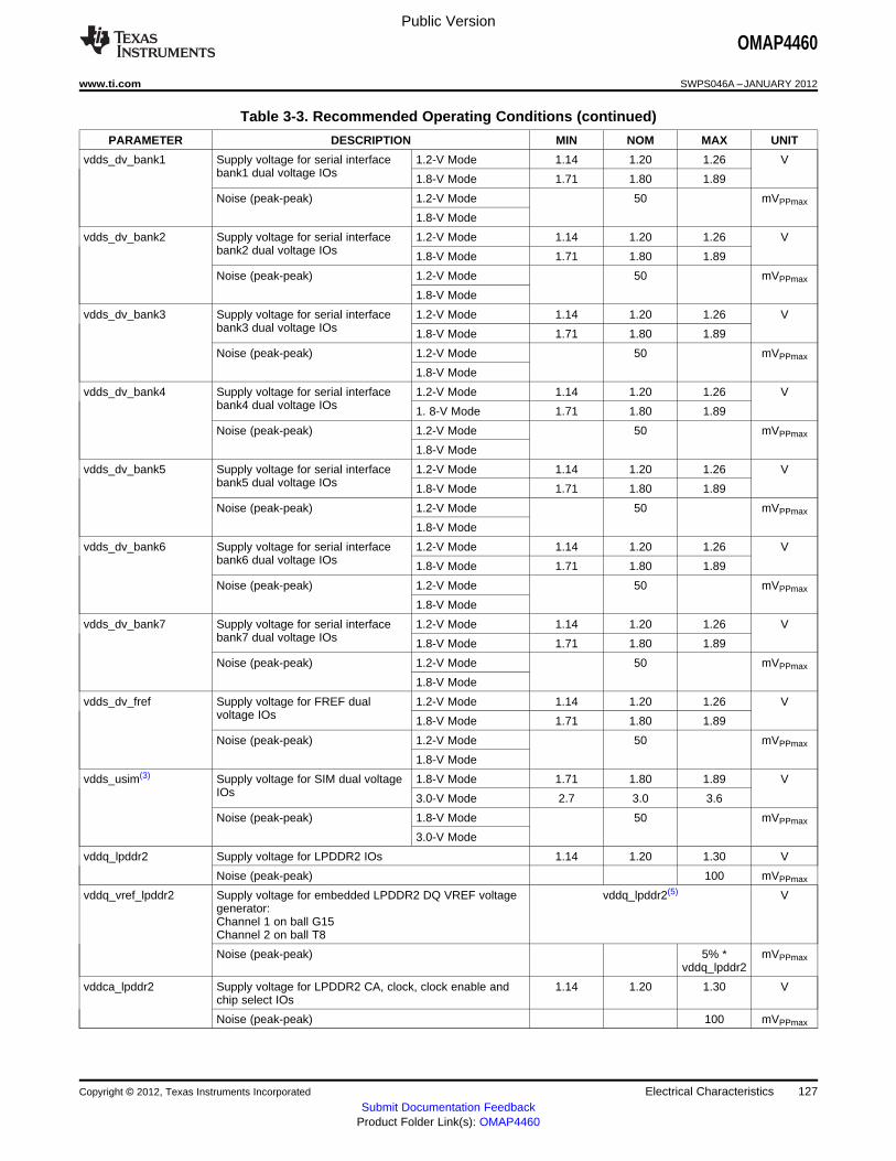
Public Version
OMAP4460
www.ti.com SWPS046A –JANUARY 2012
Table 3-3. Recommended Operating Conditions (continued)
PARAMETER DESCRIPTION MIN NOM MAX UNIT
vdds_dv_bank1 Supply voltage for serial interface 1.2-V Mode 1.14 1.20 1.26 Vbank1 dual voltage IOs 1.8-V Mode 1.71 1.80 1.89
Noise (peak-peak) 1.2-V Mode 50 mVPPmax
1.8-V Mode
vdds_dv_bank2 Supply voltage for serial interface 1.2-V Mode 1.14 1.20 1.26 Vbank2 dual voltage IOs 1.8-V Mode 1.71 1.80 1.89
Noise (peak-peak) 1.2-V Mode 50 mVPPmax
1.8-V Mode
vdds_dv_bank3 Supply voltage for serial interface 1.2-V Mode 1.14 1.20 1.26 Vbank3 dual voltage IOs 1.8-V Mode 1.71 1.80 1.89
Noise (peak-peak) 1.2-V Mode 50 mVPPmax
1.8-V Mode
vdds_dv_bank4 Supply voltage for serial interface 1.2-V Mode 1.14 1.20 1.26 Vbank4 dual voltage IOs 1. 8-V Mode 1.71 1.80 1.89
Noise (peak-peak) 1.2-V Mode 50 mVPPmax
1.8-V Mode
vdds_dv_bank5 Supply voltage for serial interface 1.2-V Mode 1.14 1.20 1.26 Vbank5 dual voltage IOs 1.8-V Mode 1.71 1.80 1.89
Noise (peak-peak) 1.2-V Mode 50 mVPPmax
1.8-V Mode
vdds_dv_bank6 Supply voltage for serial interface 1.2-V Mode 1.14 1.20 1.26 Vbank6 dual voltage IOs 1.8-V Mode 1.71 1.80 1.89
Noise (peak-peak) 1.2-V Mode 50 mVPPmax
1.8-V Mode
vdds_dv_bank7 Supply voltage for serial interface 1.2-V Mode 1.14 1.20 1.26 Vbank7 dual voltage IOs 1.8-V Mode 1.71 1.80 1.89
Noise (peak-peak) 1.2-V Mode 50 mVPPmax
1.8-V Mode
vdds_dv_fref Supply voltage for FREF dual 1.2-V Mode 1.14 1.20 1.26 Vvoltage IOs 1.8-V Mode 1.71 1.80 1.89
Noise (peak-peak) 1.2-V Mode 50 mVPPmax
1.8-V Mode
vdds_usim(3) Supply voltage for SIM dual voltage 1.8-V Mode 1.71 1.80 1.89 VIOs 3.0-V Mode 2.7 3.0 3.6
Noise (peak-peak) 1.8-V Mode 50 mVPPmax
3.0-V Mode
vddq_lpddr2 Supply voltage for LPDDR2 IOs 1.14 1.20 1.30 V
Noise (peak-peak) 100 mVPPmax
vddq_vref_lpddr2 Supply voltage for embedded LPDDR2 DQ VREF voltage vddq_lpddr2(5) Vgenerator:Channel 1 on ball G15Channel 2 on ball T8
Noise (peak-peak) 5% * mVPPmaxvddq_lpddr2
vddca_lpddr2 Supply voltage for LPDDR2 CA, clock, clock enable and 1.14 1.20 1.30 Vchip select IOs
Noise (peak-peak) 100 mVPPmax
Copyright © 2012, Texas Instruments Incorporated Electrical Characteristics 127Submit Documentation Feedback
Product Folder Link(s): OMAP4460
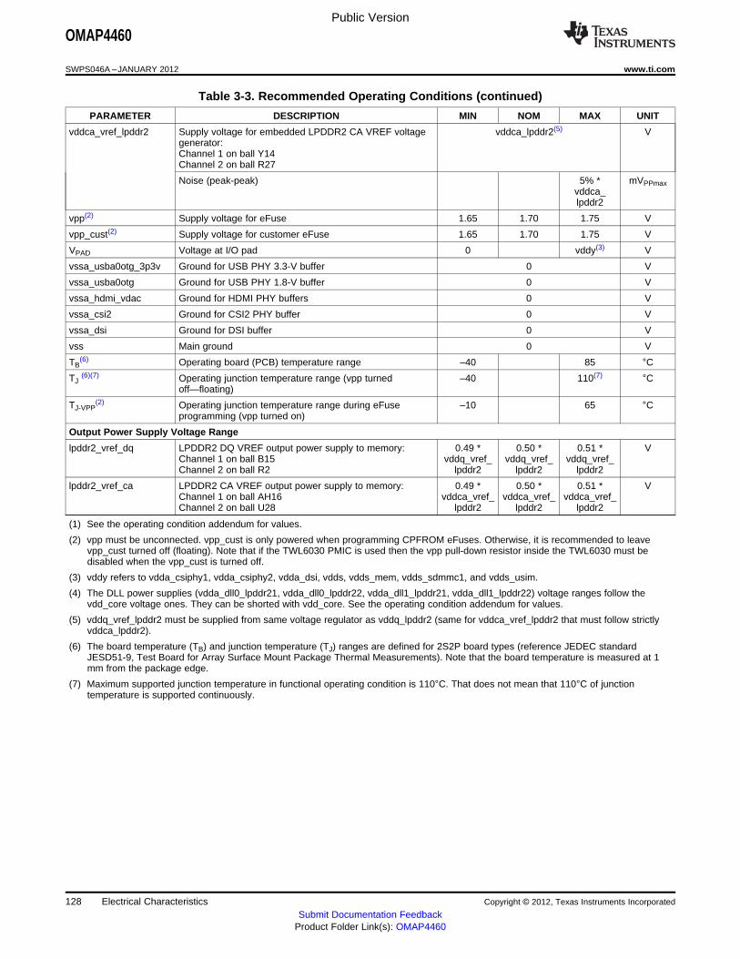
Public Version
OMAP4460
SWPS046A –JANUARY 2012 www.ti.com
Table 3-3. Recommended Operating Conditions (continued)
PARAMETER DESCRIPTION MIN NOM MAX UNIT
vddca_vref_lpddr2 Supply voltage for embedded LPDDR2 CA VREF voltage vddca_lpddr2(5) Vgenerator:Channel 1 on ball Y14Channel 2 on ball R27
Noise (peak-peak) 5% * mVPPmaxvddca_lpddr2
vpp(2) Supply voltage for eFuse 1.65 1.70 1.75 V
vpp_cust(2) Supply voltage for customer eFuse 1.65 1.70 1.75 V
VPAD Voltage at I/O pad 0 vddy(3) V
vssa_usba0otg_3p3v Ground for USB PHY 3.3-V buffer 0 V
vssa_usba0otg Ground for USB PHY 1.8-V buffer 0 V
vssa_hdmi_vdac Ground for HDMI PHY buffers 0 V
vssa_csi2 Ground for CSI2 PHY buffer 0 V
vssa_dsi Ground for DSI buffer 0 V
vss Main ground 0 V
TB(6) Operating board (PCB) temperature range –40 85 °C
TJ(6)(7) Operating junction temperature range (vpp turned –40 110(7) °C
off—floating)
TJ-VPP(2) Operating junction temperature range during eFuse –10 65 °C
programming (vpp turned on)
Output Power Supply Voltage Range
lpddr2_vref_dq LPDDR2 DQ VREF output power supply to memory: 0.49 * 0.50 * 0.51 * VChannel 1 on ball B15 vddq_vref_ vddq_vref_ vddq_vref_Channel 2 on ball R2 lpddr2 lpddr2 lpddr2
lpddr2_vref_ca LPDDR2 CA VREF output power supply to memory: 0.49 * 0.50 * 0.51 * VChannel 1 on ball AH16 vddca_vref_ vddca_vref_ vddca_vref_Channel 2 on ball U28 lpddr2 lpddr2 lpddr2
(1) See the operating condition addendum for values.
(2) vpp must be unconnected. vpp_cust is only powered when programming CPFROM eFuses. Otherwise, it is recommended to leavevpp_cust turned off (floating). Note that if the TWL6030 PMIC is used then the vpp pull-down resistor inside the TWL6030 must bedisabled when the vpp_cust is turned off.
(3) vddy refers to vdda_csiphy1, vdda_csiphy2, vdda_dsi, vdds, vdds_mem, vdds_sdmmc1, and vdds_usim.
(4) The DLL power supplies (vdda_dll0_lpddr21, vdda_dll0_lpddr22, vdda_dll1_lpddr21, vdda_dll1_lpddr22) voltage ranges follow thevdd_core voltage ones. They can be shorted with vdd_core. See the operating condition addendum for values.
(5) vddq_vref_lpddr2 must be supplied from same voltage regulator as vddq_lpddr2 (same for vddca_vref_lpddr2 that must follow strictlyvddca_lpddr2).
(6) The board temperature (TB) and junction temperature (TJ) ranges are defined for 2S2P board types (reference JEDEC standardJESD51-9, Test Board for Array Surface Mount Package Thermal Measurements). Note that the board temperature is measured at 1mm from the package edge.
(7) Maximum supported junction temperature in functional operating condition is 110°C. That does not mean that 110°C of junctiontemperature is supported continuously.
128 Electrical Characteristics Copyright © 2012, Texas Instruments Incorporated
Submit Documentation FeedbackProduct Folder Link(s): OMAP4460

Public Version
OMAP4460
www.ti.com SWPS046A –JANUARY 2012
3.3 DC Electrical Characteristics
Table 3-4 through Table 3-20 summarize the dc electrical characteristics.
NOTEThe data specified in Table 3-4 through Table 3-20 are subject to change.
NOTEThe interfaces or signals described in Table 3-4 through Table 3-20 correspond to theinterfaces or signals available in multiplexing mode 0.
All interfaces or signals multiplexed on the balls / pins described in these tables have thesame dc electrical characteristics, unless multiplexing involves a PHY/GPIO combination inwhich case different dc electrical characteristics are specified for the different multiplexingmodes.
NOTEIn the following tables, VOL and VOH are JEDEC (JESD8-7A) compliant that means:
Normal range of VOH / VOL are [VDDS – 0.45V] / 0.45 V respectively, for IOH / IOL = 2 mA
Wide range is VOH / VOL = [VDDS – 0.2 V] / 0.2 V respectively, for IOH / IOL = 100 µA
Except for the following signals:
• hdmi_ddc_scl, hdmi_ddc_sda, 2c[1:4]_scl, i2c[1:4]_sda, sr_scl, sr_sda in I2C mode
(Balls: A8 / B8 / AE28 / AE26 / C26 / D26 / W27 / Y27 / AG21 / AH22 / AG9 / AF9)
• dsi1_dy[0:4], dsi1_dy[0:4], dsi1_dy[0:2], dsi1_dy[0:2]
(Balls: P3 / P4 / N3 / N4 / M3 / M4 / L3 / L4 / K3 / K4 / T3 / T4 / U3 / U4 / V3 / V4)
• hdmi_data[0:2]x, hdmi_data[0:2]y, hdmi_clockx, hdmi_clocky
(Balls: C8 / D8 / C9 / D9 / C10 / D10 / C11 / D11)
• usba0_otg_dp, usba0_otg_dm (Balls: B5 / B4) in USB PHY mode
• fref_xtal_out (Ball: AH5)
• kpd_col[7-0]
(Balls: C20 / AH19 / B21 / AF20 / A21 / AE21 / B20 / H26 / H27 / B19 / G25 / J27 / D19 /G26 / H25 / C19 / H26 / H27 / D18 / G25 / J27 / C18 / G26 / H25)
• hdq_sio (Ball: AA29)
• sys_nreswarm (Ball: AF7)
• usbc1_icusb_dm, usbc1_icusb_dp (Balls: H3 / AF5, H2 / AE5)
3.3.1 GPMC DC Electrical Characteristics
Table 3-4 summarizes the GPMC dc electrical characteristics in multiplexing mode 0.
NOTEFor more information on the IO cell configurations (SC[1:0], MB[1:0] and LB0), see theControl Module / Control Module Functional Description / Functional Register Description /Signal Integrity Parameter Control Registers With Pad Group Assignment section of theOMAP4460 TRM.
Copyright © 2012, Texas Instruments Incorporated Electrical Characteristics 129Submit Documentation Feedback
Product Folder Link(s): OMAP4460
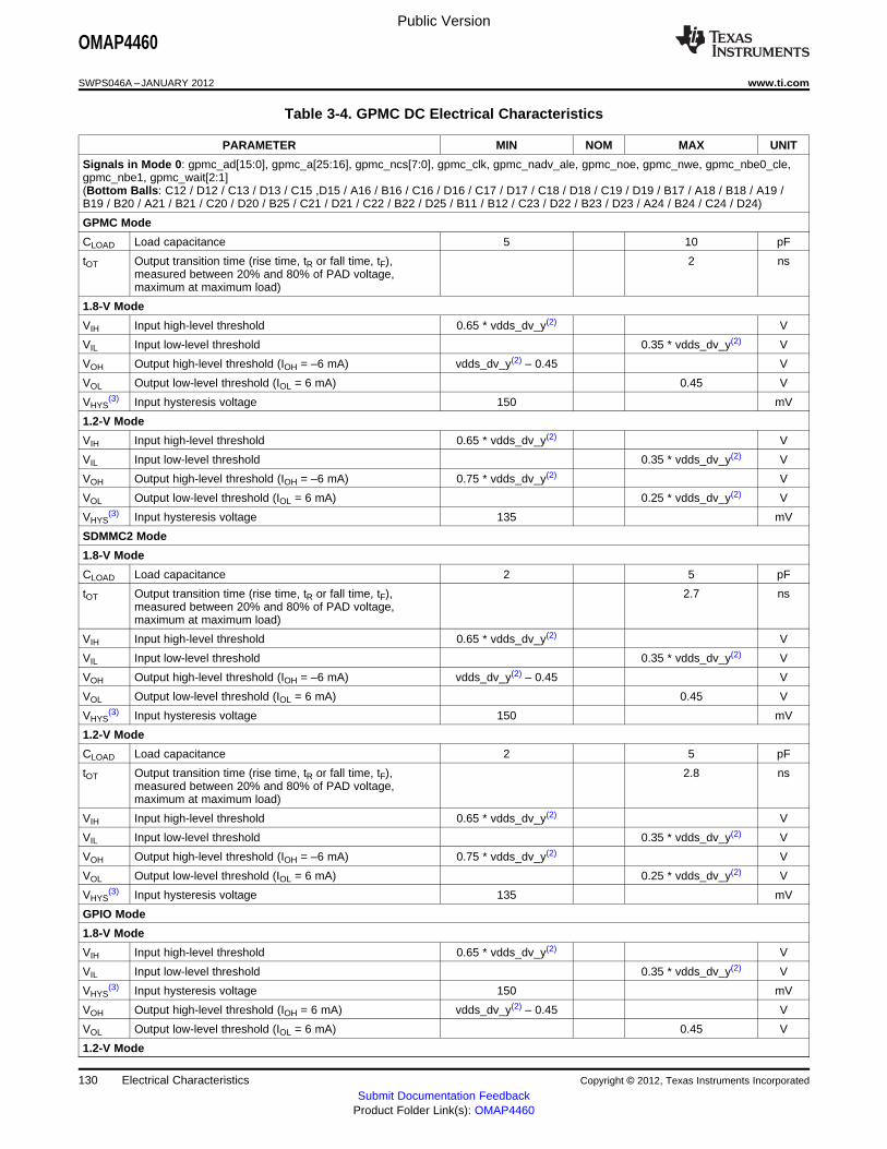
Public Version
OMAP4460
SWPS046A –JANUARY 2012 www.ti.com
Table 3-4. GPMC DC Electrical Characteristics
PARAMETER MIN NOM MAX UNIT
Signals in Mode 0: gpmc_ad[15:0], gpmc_a[25:16], gpmc_ncs[7:0], gpmc_clk, gpmc_nadv_ale, gpmc_noe, gpmc_nwe, gpmc_nbe0_cle,gpmc_nbe1, gpmc_wait[2:1](Bottom Balls: C12 / D12 / C13 / D13 / C15 ,D15 / A16 / B16 / C16 / D16 / C17 / D17 / C18 / D18 / C19 / D19 / B17 / A18 / B18 / A19 /B19 / B20 / A21 / B21 / C20 / D20 / B25 / C21 / D21 / C22 / B22 / D25 / B11 / B12 / C23 / D22 / B23 / D23 / A24 / B24 / C24 / D24)
GPMC Mode
CLOAD Load capacitance 5 10 pF
tOT Output transition time (rise time, tR or fall time, tF), 2 nsmeasured between 20% and 80% of PAD voltage,maximum at maximum load)
1.8-V Mode
VIH Input high-level threshold 0.65 * vdds_dv_y(2) V
VIL Input low-level threshold 0.35 * vdds_dv_y(2) V
VOH Output high-level threshold (IOH = –6 mA) vdds_dv_y(2) – 0.45 V
VOL Output low-level threshold (IOL = 6 mA) 0.45 V
VHYS(3) Input hysteresis voltage 150 mV
1.2-V Mode
VIH Input high-level threshold 0.65 * vdds_dv_y(2) V
VIL Input low-level threshold 0.35 * vdds_dv_y(2) V
VOH Output high-level threshold (IOH = –6 mA) 0.75 * vdds_dv_y(2) V
VOL Output low-level threshold (IOL = 6 mA) 0.25 * vdds_dv_y(2) V
VHYS(3) Input hysteresis voltage 135 mV
SDMMC2 Mode
1.8-V Mode
CLOAD Load capacitance 2 5 pF
tOT Output transition time (rise time, tR or fall time, tF), 2.7 nsmeasured between 20% and 80% of PAD voltage,maximum at maximum load)
VIH Input high-level threshold 0.65 * vdds_dv_y(2) V
VIL Input low-level threshold 0.35 * vdds_dv_y(2) V
VOH Output high-level threshold (IOH = –6 mA) vdds_dv_y(2) – 0.45 V
VOL Output low-level threshold (IOL = 6 mA) 0.45 V
VHYS(3) Input hysteresis voltage 150 mV
1.2-V Mode
CLOAD Load capacitance 2 5 pF
tOT Output transition time (rise time, tR or fall time, tF), 2.8 nsmeasured between 20% and 80% of PAD voltage,maximum at maximum load)
VIH Input high-level threshold 0.65 * vdds_dv_y(2) V
VIL Input low-level threshold 0.35 * vdds_dv_y(2) V
VOH Output high-level threshold (IOH = –6 mA) 0.75 * vdds_dv_y(2) V
VOL Output low-level threshold (IOL = 6 mA) 0.25 * vdds_dv_y(2) V
VHYS(3) Input hysteresis voltage 135 mV
GPIO Mode
1.8-V Mode
VIH Input high-level threshold 0.65 * vdds_dv_y(2) V
VIL Input low-level threshold 0.35 * vdds_dv_y(2) V
VHYS(3) Input hysteresis voltage 150 mV
VOH Output high-level threshold (IOH = 6 mA) vdds_dv_y(2) – 0.45 V
VOL Output low-level threshold (IOL = 6 mA) 0.45 V
1.2-V Mode
130 Electrical Characteristics Copyright © 2012, Texas Instruments Incorporated
Submit Documentation FeedbackProduct Folder Link(s): OMAP4460

Public Version
OMAP4460
www.ti.com SWPS046A –JANUARY 2012
Table 3-4. GPMC DC Electrical Characteristics (continued)
PARAMETER MIN NOM MAX UNIT
VIH Input high-level threshold 0.7 * vdds_dv_y(2) V
VIL Input low-level threshold 0.3 * vdds_dv_y(2) V
VHYS(3) Input hysteresis voltage 130 mV
VOH Output high-level threshold (IOH = 6 mA) 0.75 * vdds_dv_y(2) V
VOL Output low-level threshold (IOL = 6 mA) 0.25 * vdds_dv_y(2) V
Signal in Mode 0: gpmc_wait0(Bottom Ball: B26)
CLOAD Load capacitance SC[1:0] = 00 4 60 pF
SC[1:0] = 01 2 21
SC[1:0] = 10 7 33
tOT Output transition time (rise time, tR or fall SC[1:0] = 00 1 15 nstime, tF) measured between 10% to 90% SC[1:0] = 01 0.4 5of PAD voltage, minimum at the
SC[1:0] = 10 0.6 7minimum load and maximum at themaximum load
1.2-V Mode
VIH Input high-level threshold 0.65 * vdds_dv_gpmc vdds_dv_gpmc + 0.3 V
VIL Input low-level threshold –0.3 0.35 * vdds_dv_gpmc V
VHYS(3) Input hysteresis voltage 135 mV
VOH Output high-level threshold (IOH = –4 mA) 0.75 * vdds_dv_gpmc V
VOL Output low-level threshold (IOL = 4 mA) 0.25 * vdds_dv_gpmc V
1.8-V Mode
VIH Input high-level threshold 0.65 * vdds_dv_gpmc vdds_dv_gpmc + 0.3 V
VIL Input low-level threshold –0.3 0.35 * vdds_dv_gpmc V
VHYS(3) Input hysteresis voltage 150 mV
VOH Output high-level threshold (IOH = –4 mA) vdds_dv_gpmc – 0.45 V
VOL Output low-level threshold (IOL = 4 mA) 0.45 V
Signal in Mode 0: gpmc_nwp(Bottom Ball: C25)
Copyright © 2012, Texas Instruments Incorporated Electrical Characteristics 131Submit Documentation Feedback
Product Folder Link(s): OMAP4460

Public Version
OMAP4460
SWPS046A –JANUARY 2012 www.ti.com
Table 3-4. GPMC DC Electrical Characteristics (continued)
PARAMETER MIN NOM MAX UNIT
CLOAD(4) Load capacitance MB[1:0] = 11 LB0 = 1 (Mode1) 20 25 pF
maximum frequency = 24 MHztransmission line delay = 670 ps
MB[1:0] = 11 LB0 = 1 (Mode1) 2 5maximum frequency = 60 MHztransmission line delay = 335 ps
MB[1:0] = 01 LB0 = 0 (Mode2) 14 17maximum frequency = 25 MHztransmission line delay = 335 ps
MB[1:0] = 01 LB0 = 0 (Mode2) 2 5maximum frequency = 48 MHztransmission line delay = 536 ps
MB[1:0] = 10 LB0 = 1 (Mode3) 23 28maximum frequency = 20 MHztransmission line delay = 838 ps
MB[1:0] = 10 LB0 = 1 (Mode3) 16 20maximum frequency = 24 MHztransmission line delay = 670 ps
MB[1:0] = 10 LB0 = 0 (Mode4) 16 20maximum frequency = 4 MHztransmission line delay = 1675 ps
MB[1:0] = 10 LB0 = 0 (Mode4) 2 5maximum frequency = 25 MHztransmission line delay = 670 ps
MB[1:0] = 10 LB0 = 0 (Mode4) 5 7maximum frequency = 25 MHztransmission line delay = 670 ps
MB[1:0] = 10 LB0 = 0 (Mode4) 2 11maximum frequency = 25 MHztransmission line delay = 536 ps
tOT(4) Output transition MB[1:0] = 11 LB0 = 1 (Mode1) 10 ns
time (rise time, tR maximum frequency = 24 MHzor fall time, tF) transmission line delay = 670 psmeasured between MB[1:0] = 11 LB0 = 1 (Mode1) 410% to 90% of maximum frequency = 60 MHzPAD voltage, transmission line delay = 335 psmaximum at the
MB[1:0] = 01 LB0 = 0 (Mode2) 5.6(1)maximum loadmaximum frequency = 25 MHztransmission line delay = 335 ps
MB[1:0] = 01 LB0 = 0 (Mode2) 6.3maximum frequency = 48 MHztransmission line delay = 536 ps
MB[1:0] = 10 LB0 = 1 (Mode3) 10.5(1)
maximum frequency = 20 MHztransmission line delay = 838 ps
MB[1:0] = 10 LB0 = 1 (Mode3) 12.5maximum frequency = 24 MHztransmission line delay = 670 ps
MB[1:0] = 10 LB0 = 0 (Mode4) 16.8(1)
maximum frequency = 4 MHztransmission line delay = 1675 ps
MB[1:0] = 10 LB0 = 0 (Mode4) 10maximum frequency = 25 MHztransmission line delay = 670 ps
MB[1:0] = 10 LB0 = 0 (Mode4) 12.2maximum frequency = 25 MHztransmission line delay = 670 ps
MB[1:0] = 10 LB0 = 0 (Mode4) 8(1)
maximum frequency = 25 MHztransmission line delay = 536 ps
132 Electrical Characteristics Copyright © 2012, Texas Instruments Incorporated
Submit Documentation FeedbackProduct Folder Link(s): OMAP4460
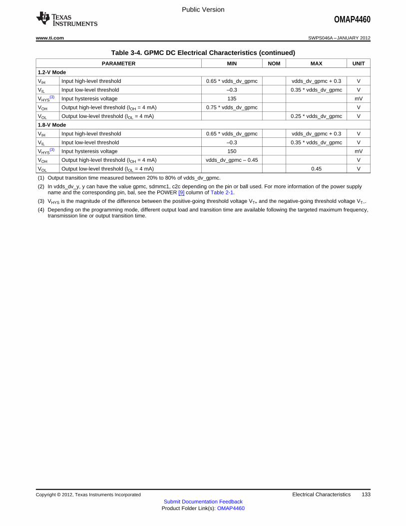
Public Version
OMAP4460
www.ti.com SWPS046A –JANUARY 2012
Table 3-4. GPMC DC Electrical Characteristics (continued)
PARAMETER MIN NOM MAX UNIT
1.2-V Mode
VIH Input high-level threshold 0.65 * vdds_dv_gpmc vdds_dv_gpmc + 0.3 V
VIL Input low-level threshold –0.3 0.35 * vdds_dv_gpmc V
VHYS(3) Input hysteresis voltage 135 mV
VOH Output high-level threshold (IOH = 4 mA) 0.75 * vdds_dv_gpmc V
VOL Output low-level threshold (IOL = 4 mA) 0.25 * vdds_dv_gpmc V
1.8-V Mode
VIH Input high-level threshold 0.65 * vdds_dv_gpmc vdds_dv_gpmc + 0.3 V
VIL Input low-level threshold –0.3 0.35 * vdds_dv_gpmc V
VHYS(3) Input hysteresis voltage 150 mV
VOH Output high-level threshold (IOH = 4 mA) vdds_dv_gpmc – 0.45 V
VOL Output low-level threshold (IOL = 4 mA) 0.45 V
(1) Output transition time measured between 20% to 80% of vdds_dv_gpmc.
(2) In vdds_dv_y, y can have the value gpmc, sdmmc1, c2c depending on the pin or ball used. For more information of the power supplyname and the corresponding pin, bal, see the POWER [9] column of Table 2-1.
(3) VHYS is the magnitude of the difference between the positive-going threshold voltage VT+ and the negative-going threshold voltage VT–.
(4) Depending on the programming mode, different output load and transition time are available following the targeted maximum frequency,transmission line or output transition time.
Copyright © 2012, Texas Instruments Incorporated Electrical Characteristics 133Submit Documentation Feedback
Product Folder Link(s): OMAP4460
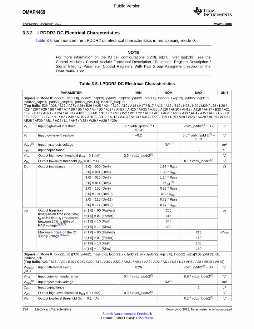
Public Version
OMAP4460
SWPS046A –JANUARY 2012 www.ti.com
3.3.2 LPDDR2 DC Electrical Characteristics
Table 3-5 summarizes the LPDDR2 dc electrical characteristics in multiplexing mode 0.
NOTEFor more information on the IO cell configurations (i[2:0], sr[1:0], vref_tap[1:0]), see theControl Module / Control Module Functional Description / Functional Register Description /Signal Integrity Parameter Control Registers With Pad Group Assignment section of theOMAP4460 TRM.
Table 3-5. LPDDR2 DC Electrical Characteristics
PARAMETER MIN NOM MAX UNIT
Signals in Mode 0: lpddr21_dq[31:0], lpddr21_ca[9:0], lpddr21_dm[3:0], lpddr21_ncs[1:0], lpddr21_cke[1:0], lpddr22_dq[31:0],lpddr22_ca[9:0], lpddr22_dm[9:0], lpddr22_ncs[1:0], lpddr22_cke[1:0](Top Balls: E29 / D28 / B27 / A27 / A26 / B26 / A25 / A24 / B19 / A19 / A18 / A17 / B17 / A13 / A12 / B12 / N28 / N29 / M29 / L28 / K28 /K29 / J29 / H29 / B8 / A8 / A7 / B6 / B5 / A5 / A4 / B3 / AJ27 / AH27 / AH26 / AH25 / AJ25 / AJ20 / AH20 / AH19 / AJ18 / AH17 / B22 / A21/ F28 / B11 / AH24 / AJ24 / AH23 / AJ23 / L2 / M1 / N1 / U2 / V1 / W2 / W1 / Y2 / AE1 / AF1 / AG1 / AG2 / AJ3 / AH4 / AJ5 / AH6 / C2 / D1/ E1 / E2 / F2 / G1 / H1 / H2 / AJ9 / AJ10 / AH10 / AH11 / AJ12 / AJ13 / AH13 / AJ14 / R29 / T29 / U29 / V29 / W28 / AC29 / AD29 / AD28 /AE28 / AF29 / AB1 / AC2 / L1 / AH7 / Y28 / W29 / AA29 / Y29)
VIH Input high-level threshold 0.5 * vddx_lpddr2(7) + vddx_lpddr2(7) + 0.2 V0.13
VIL Input low-level threshold –0.2 0.5 * vddx_lpddr2(7) – V0.13
VHYS(1) Input hysteresis voltage NA(1) mV
CIN Input capacitance 3 pF
VOH Output high-level threshold (IOH = 0.1 mA) 0.9 * vddx_lpddr2(7) V
VOL Output low-level threshold (IOL = 0.1 mA) 0.1 * vddx_lpddr2(7) V
ZO Output impedance i[2:0] = 000 (Drv5) 1.66 * RREF Ωi[2:0] = 001 (Drv6) 1.33 * RREF
i[2:0] = 010 (Drv7) 1.14 * RREF
i[2:0] = 011 (Drv8) RREF(2)
i[2:0] = 100 (Drv9) 0.88 * RREF
i[2:0] = 101 (Drv10) 0.8 * RREF
i[2:0] = 110 (Drv11) 0.73 * RREF
i[2:0] = 111 (Drv12) 0.67 * RREF
tOT Output transition sr[1:0] = 00 (Fastest) 250 pstime/turn-on time (rise time, sr[1:0] = 01 (Faster) 315tR or fall time, tF) measured
sr[1:0] = 10 (Fast) 340between 10% to 90% ofPAD voltage(3)(4)(6)
sr[1:0] = 11 (Slow) 390
Maximum noise on the IO sr[1:0] = 00 (Fastest) 215 mVPPsupply voltage(3)(5)(6)
sr[1:0] = 01 (Faster) 110
sr[1:0] = 10 (Fast) 108
sr[1:0] = 11 (Slow) 110
Signals in Mode 0: lpddr21_dqs[3:0], lpddr21_ndqs[3:0], lpddr21_ck, lpddr21_nck, lpddr22_dqs[3:0], lpddr22_ndqs[3:0], lpddr22_ck,lpddr22_nck(Top Balls: A23 / B23 / A20 / B20 / G28 / G29 / B10 / A10 / AJ21 / AH21 / AA1 / AA2 / AD2 / AD1 / K2 / K1 / AH8 / AJ8 / AB28 / AB29)
VSWING Input differential swing 0.26 vddx_lpddr2(7) + 0.4 V(DC)
VCM Input common mode range 0.4 * vddx_lpddr2(7) 0.6 * vddx_lpddr2(7) V
VHYS(1) Input hysteresis voltage NA(1) mV
CIN Input capacitance 3 pF
VOH Output high-level threshold (IOH = 0.1 mA) 0.9 * vddx_lpddr2(7) V
VOL Output low-level threshold (IOL = 0.1 mA) 0.1 * vddx_lpddr2(7) V
134 Electrical Characteristics Copyright © 2012, Texas Instruments Incorporated
Submit Documentation FeedbackProduct Folder Link(s): OMAP4460

Public Version
OMAP4460
www.ti.com SWPS046A –JANUARY 2012
Table 3-5. LPDDR2 DC Electrical Characteristics (continued)
PARAMETER MIN NOM MAX UNIT
ZO Output impedance i[2:0] = 000 (Drv5) 1.66 * RREF Ωi[2:0] = 001 (Drv6) 1.33 * RREF
i[2:0] = 010 (Drv7) 1.14 * RREF
i[2:0] = 011 (Drv8) RREF(2)
i[2:0] = 100 (Drv9) 0.88 * RREF
i[2:0] = 101 (Drv10) 0.8 * RREF
i[2:0] = 110 (Drv11) 0.73 * RREF
i[2:0] = 111 (Drv12) 0.67 * RREF
tOT Output transition sr[1:0] = 00 (Fastest) 250 pstime/turn-on time (rise time, sr[1:0] = 01 (Faster) 315tR or fall time, tF) measured
sr[1:0] = 10 (Fast) 340between 10% to 90% ofPAD voltage(3)(4)(6)
sr[1:0] = 11 (Slow) 390
Maximum noise on the IO sr[1:0] = 00 (Fastest) 215 mVPPsupply voltage(3)(5)(6)
sr[1:0] = 01 (Faster) 110
sr[1:0] = 10 (Fast) 108
sr[1:0] = 11 (Slow) 110
Signals in Mode 0: lpddr21_vref_ca, lpddr21_vref_dq, lpddr22_vref_ca, lpddr22_vref_dq(Top Balls: AH16 / B15 / U28 / R2)
VREF Reference generation dc vref_tap[1:0] = 00 0.495 * 0.500 * 0.505 * Vvoltage level (Mint_2ua mode) vddy_vref_lpddr2(8) vddy_vref_ vddy_vref_lpddr2(8)
lpddr2(8)
vref_tap[1:0] = 01 0.492 * 0.500 * 0.508 *(Mint_4ua mode) vddy_vref_lpddr2(8) vddy_vref_ vddy_vref_lpddr2(8)
lpddr2(8)
vref_tap[1:0] = 10 0.490 * 0.500 * 0.510 *(Mint_6ua mode) vddy_vref_lpddr2(8) vddy_vref_ vddy_vref_lpddr2(8)
lpddr2(8)
vref_tap[1:0] = 11 0.490 * 0.500 * 0.510 *(Mint_8ua mode) vddy_vref_lpddr2(8) vddy_vref_ vddy_vref_lpddr2(8)
lpddr2(8)
(1) This buffer is designed for high-speed application. In high-speed mode, it is fast enough to avoid any noise on the signal duringtransition and then hysteresis is not required.
(2) RREF (reference output impedance) is considered to be the production trimming setting for Drv8 mode, with RREF = 50 Ω, whichcorresponds to ZO = 50 Ω (IOUT = 8 mA). For a full description of the output impedance setting, see the the Control Module / ControlModule Functional Description / Functional Register Description / Signal Integrity Parameter Control Registers With Pad GroupAssignment section of the OMAP4460 TRM.
(3) To achieve optimal noise/speed trade off, the slew rate (turn-on time) of the output signal can be programmed using the slew ratecontrol bits sr[1:0]. Please note that the control bits sr[1:0] do not affect the driver DC drive-strength. They only control the driver turn-ontime. It is to be noted that turn-on time and maximum supply noise are the parameter defined to help user make relative comparison andcorrelate the driver operation at different turn-on time settings.
(4) Output transition time/turn-on time for Drv8 setting, i[2:0] = 011. For a full description of this setting, see the Control Module / ControlModule Functional Description / Functional Register Description / Signal Integrity Parameter Control Registers With Pad GroupAssignment section of the OMAP4460 TRM.
(5) Maximum noise (peak-peak) on the IO supply voltage for Drv8 setting, i[2:0] = 011.
(6) The measurement setup (see Figure 3-1 and Figure 3-2) is not intended as a precise representation of any particular systemenvironment or a depiction of the actual load presented. Maximum output supply noise (see Figure 3-2, L*di/dt) on the IO supply ismeasured with 1 nH of inductance on the IO supply.
(7) vddx_lpddr2 can have the value vddq_lpddr2, vddca_lpddr21, vddca_lpddr22 depending on the ball used. For more information of thepower supply name and the corresponding pin, ball, see the POWER [9] column of Table 2-1.
(8) vddy_vref_lpddr2 can have the value vddca_vref_lpddr21, vddca_lpddr22, vddq_vref_lpddr21, vddq_vref_lpddr22 depending on the ballused. For more information of the power supply name and the corresponding pin, ball, see the POWER [9] column of Table 2-1.
Copyright © 2012, Texas Instruments Incorporated Electrical Characteristics 135Submit Documentation Feedback
Product Folder Link(s): OMAP4460

Pad
Rload Pad
RloadTx
Rdrv
Rdrv
Tx
vdds
vss
Vdds/2
Pulldown Turn-ontime measurement
Pullup Turn-ontime measurement
• R is kept equal to average R value for a given drive-strength setting level.load drv
• Turn-on time is measured as time between 10% to 90% of the signal swing on pad.
a
a
SWPS040-121
A[0--> 1]
VDDS
VSS
VSSS_L
1 nH VSS
5 pF Load
1 nH
VDDS_L
PADDriver
SWPS040-122
Public Version
OMAP4460
SWPS046A –JANUARY 2012 www.ti.com
Figure 3-1. Output Turn-on Time Measurement
Figure 3-2. Output Supply Noise Measurement Setup(1)(2)
(1) Maximum supply noise = VDDS – minimum (VDDS_L – VSSS_L)
(2) 1 nH is used for a typical package inductance on the supplies.
136 Electrical Characteristics Copyright © 2012, Texas Instruments Incorporated
Submit Documentation FeedbackProduct Folder Link(s): OMAP4460
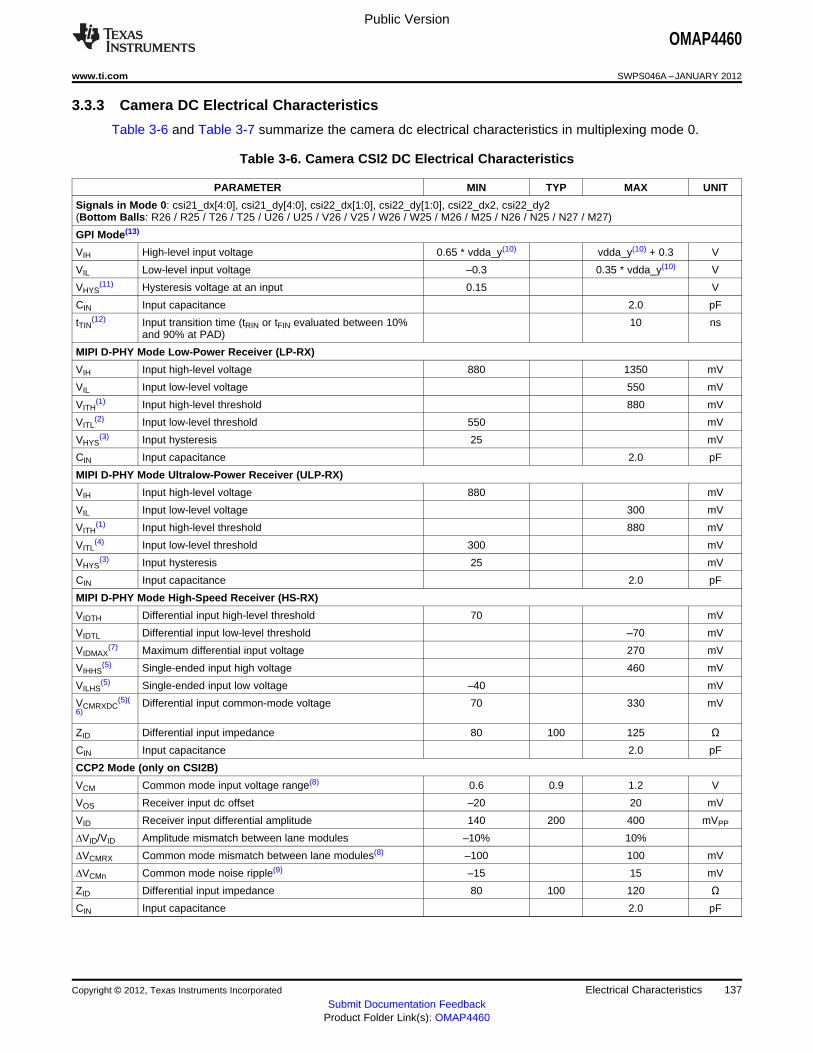
Public Version
OMAP4460
www.ti.com SWPS046A –JANUARY 2012
3.3.3 Camera DC Electrical Characteristics
Table 3-6 and Table 3-7 summarize the camera dc electrical characteristics in multiplexing mode 0.
Table 3-6. Camera CSI2 DC Electrical Characteristics
PARAMETER MIN TYP MAX UNIT
Signals in Mode 0: csi21_dx[4:0], csi21_dy[4:0], csi22_dx[1:0], csi22_dy[1:0], csi22_dx2, csi22_dy2(Bottom Balls: R26 / R25 / T26 / T25 / U26 / U25 / V26 / V25 / W26 / W25 / M26 / M25 / N26 / N25 / N27 / M27)
GPI Mode(13)
VIH High-level input voltage 0.65 * vdda_y(10) vdda_y(10) + 0.3 V
VIL Low-level input voltage –0.3 0.35 * vdda_y(10) V
VHYS(11) Hysteresis voltage at an input 0.15 V
CIN Input capacitance 2.0 pF
tTIN(12) Input transition time (tRIN or tFIN evaluated between 10% 10 ns
and 90% at PAD)
MIPI D-PHY Mode Low-Power Receiver (LP-RX)
VIH Input high-level voltage 880 1350 mV
VIL Input low-level voltage 550 mV
VITH(1) Input high-level threshold 880 mV
VITL(2) Input low-level threshold 550 mV
VHYS(3) Input hysteresis 25 mV
CIN Input capacitance 2.0 pF
MIPI D-PHY Mode Ultralow-Power Receiver (ULP-RX)
VIH Input high-level voltage 880 mV
VIL Input low-level voltage 300 mV
VITH(1) Input high-level threshold 880 mV
VITL(4) Input low-level threshold 300 mV
VHYS(3) Input hysteresis 25 mV
CIN Input capacitance 2.0 pF
MIPI D-PHY Mode High-Speed Receiver (HS-RX)
VIDTH Differential input high-level threshold 70 mV
VIDTL Differential input low-level threshold –70 mV
VIDMAX(7) Maximum differential input voltage 270 mV
VIHHS(5) Single-ended input high voltage 460 mV
VILHS(5) Single-ended input low voltage –40 mV
VCMRXDC(5)( Differential input common-mode voltage 70 330 mV
6)
ZID Differential input impedance 80 100 125 ΩCIN Input capacitance 2.0 pF
CCP2 Mode (only on CSI2B)
VCM Common mode input voltage range(8) 0.6 0.9 1.2 V
VOS Receiver input dc offset –20 20 mV
VID Receiver input differential amplitude 140 200 400 mVPP
∆VID/VID Amplitude mismatch between lane modules –10% 10%
∆VCMRX Common mode mismatch between lane modules(8) –100 100 mV
∆VCMn Common mode noise ripple(9) –15 15 mV
ZID Differential input impedance 80 100 120 ΩCIN Input capacitance 2.0 pF
Copyright © 2012, Texas Instruments Incorporated Electrical Characteristics 137Submit Documentation Feedback
Product Folder Link(s): OMAP4460

Public Version
OMAP4460
SWPS046A –JANUARY 2012 www.ti.com
(1) VITH is the voltage at which the receiver is required to detect a high state in the input signal.
(2) VITL is the voltage at which the receiver is required to detect a low state in the input signal. VITL is larger than the maximum single-endedline high voltage during HS transmission. Therefore, both LP receivers will detect low during HS signaling.
(3) To reduce noise sensitivity on the received signal, the LP receiver is required to incorporate a hysteresis, VHYST.
(4) VITL is the voltage at which the receiver is required to detect a low state in the input signal. Specification is relaxed for detecting 0 duringUltralow-Power (ULP) state. The LP receiver is not required to detect HS single-ended voltage as 0 in this state.
(5) Excluding possible additional RF interference of 200 mVPP beyond 450 MHz.
(6) This value includes a ground difference of 50 mV between the transmitter and the receiver, the static common-mode level tolerance andvariations below 450 MHz.
(7) This number is the transmitter VODMAX.
(8) Common mode is defined as the average voltage level of DX and DY: VCM = (VDX + VDY)/2.
(9) Common mode ripple may be due to rise-fall time and transmission line impairments in the PCB.
(10) In vdda_y, y can have the value csi21 or csi22 depending on the ball used. For more information of the power supply name and thecorresponding pin, ball, see the POWER [9] column of Table 2-1.
(11) VHYS is the magnitude of the difference between the positive-going threshold voltage VT+ and the negative-going threshold voltage VT–.
(12) The tTIN (tRIN and tFIN also) value is the recommended condition. The tTIN (tRIN and tFIN also) mismatch causes additional delay timeinside the device then leads to ac timing invalidation in this DM. The tTIN (tRIN and tFIN also) mismatch does not necessarily meanfunctional failure. This global value may be overridden on a per basis if another value is explicitly defined for that in the TimingRequirements and Switching Characteristics Chapter of the data manual.
(13) The GPI mode is only available through multiplexing mode 3.
NOTEFor more information on the IO cell configurations (SC[1:0]), see the Control Module /Control Module Functional Description / Functional Register Description / Signal IntegrityParameter Control Registers With Pad Group Assignment section of the OMAP4460 TRM.
Table 3-7. Camera Control DC Electrical Characteristics
PARAMETER MIN NOM MAX UNIT
Signals in Mode 0: cam_shutter, cam_strobe, cam_globalreset(Bottom Balls : T27 / U27 / V27)
CLOAD Load capacitance SC[1:0] = 00 4 60 pF
SC[1:0] = 01 2 21
SC[1:0] = 10 7 33
tOT Output transition time (rise time, tR or fall SC[1:0] = 00 1 15 nstime, tF) measured between 10% to 90% of SC[1:0] = 01 0.4 5PAD voltage, minimum at the minimum load
SC[1:0] = 10 0.6 7and maximum at the maximum load
1.2-V Mode
VIH Input high-level threshold 0.65 * vdds_dv_cam vdds_dv_cam + 0.3 V
VIL Input low-level threshold –0.3 0.35 * vdds_dv_cam V
VHYS(1) Input hysteresis voltage 135 mV
VOH Output high-level threshold (IOH = –4 mA) 0.75 * vdds_dv_cam V
VOL Output low-level threshold (IOL = 4 mA) 0.25 * vdds_dv_cam V
1.8-V Mode
VIH Input high-level threshold 0.65 * vdds_dv_cam vdds_dv_cam + 0.3 V
VIL Input low-level threshold –0.3 0.35 * vdds_dv_cam V
VHYS(1) Input hysteresis voltage 150 mV
VOH Output high-level threshold (IOH = –4 mA) vdds_dv_cam – 0.45 V
VOL Output low-level threshold (IOL = 4 mA) 0.45 V
138 Electrical Characteristics Copyright © 2012, Texas Instruments Incorporated
Submit Documentation FeedbackProduct Folder Link(s): OMAP4460
Public Version
OMAP4460
www.ti.com SWPS046A –JANUARY 2012
(1) VHYS is the magnitude of the difference between the positive-going threshold voltage VT+ and the negative-going threshold voltage VT–.
Copyright © 2012, Texas Instruments Incorporated Electrical Characteristics 139Submit Documentation Feedback
Product Folder Link(s): OMAP4460

Public Version
OMAP4460
SWPS046A –JANUARY 2012 www.ti.com
3.3.4 Display DC Electrical Characteristics
Table 3-8 summarizes the display dc electrical characteristics in multiplexing mode 0.
NOTEFor more information on HDMI, please contact your TI representative.
Table 3-8. Display DSI1 DC Electrical Characteristics
PARAMETER MIN NOM MAX UNIT
Signals in Mode 0: dsi1_dx[4:0], dsi1_dy[4:0], dsi2_dx[2:0], dsi2_dy[2:0](Bottom Balls: P3 / P4 / N3 / N4 / M3 / M4 / L3 / L4 / K3 / K4 / T3 / T4 / U3 / U4 / V3 / V4)
MIPI D-PHY—High-Speed Transmitter (HS-TX) mode
|VOD|(1) High-speed transmit differential voltage 140 200 270 mV
VCMTX(1) High-speed transmit static common mode voltage 150 200 250 mV
|ΔVOD| VOD mismatch when output is differential-1 or differential-0 10 mV
|ΔVCMTX(1,0)| VCMTX mismatch when output is differential-1 or differential-0 5 mV
VOHHS(1) High-speed output high voltage 360 mV
ZOS Single-ended output impedance 40 50 62.5 ΩΔZOS Single-ended output impedance mismatch 10%
ΔVCMTX(HF) Common-level variation above 450 MHz 15 mVRMS
ΔVCMTX(LF) Common-level variation between 50 MHz and 450 MHz –50 50 mVPEAK
tTOUT Output transition time (tROUT or tFOUT evaluated between 0.15 ns20% and 80% of PAD voltage) 0.3 UI
MIPI D-PHY—Low-Power Transmitter (LP-TX) mode
VOL Thevenin output low level –50 50 mV
VOH Thevenin output high level 1.1 1.2 1.3 V
ZOLP Output impedance of LP transmitter 110 ΩtTOUT Output transition time (tROUT or tFOUT evaluated between 25 ns
20% and 80% of PAD voltage)
MIPI D-PHY—Low-Power Receiver (LP-RX) Mode
VIH Input high-level voltage 880 mV
VIL Input low-level voltage 550 mV
VITH(2) Input high-level threshold 880 mV
VITL(3) Input low-level threshold 550 mV
VHYS(4) Input hysteresis 25 mV
MIPI D-PHY Mode Ultralow-Power Receiver (ULP-RX)
VIH Input high-level voltage 880 mV
VIL Input low-level voltage 300 mV
VITH(2) Input high-level threshold 880 mV
VITL(5) Input low-level threshold 300 mV
VHYS(4) Input hysteresis 25 mV
MIPI D-PHY Mode Low Power Contention Detector (LPCD)
VIHCD High-level input voltage 450 mV
VILCD Low-level input voltage 200 mV
(1) Value when driving into differential load impedance anywhere in the range of 80 to 125 Ω. See Chapter 8 of the MIPI D-PHY standardv1.0 for complete specification on the electrical characteristics. The PCB interconnect must be 50-Ω transmission line on DSIdsi1_dx[4;0], DSI dsi1_dy[4;0] and DSI dsi2_dx[2;0], DSI dsi2_dy[2;0]. These lines must be well matched. See Chapter 7 of the MIPID-PHY standard v1.0 for complete specification of the Interconnect.
(2) VITH is the voltage at which the receiver is required to detect a high state in the input signal.
(3) VITL is the voltage at which the receiver is required to detect a low state in the input signal. VITL is larger than the maximum single-endedline high voltage during HS transmission. Therefore, both low-power receivers will detect low during high-speed signaling.
140 Electrical Characteristics Copyright © 2012, Texas Instruments Incorporated
Submit Documentation FeedbackProduct Folder Link(s): OMAP4460
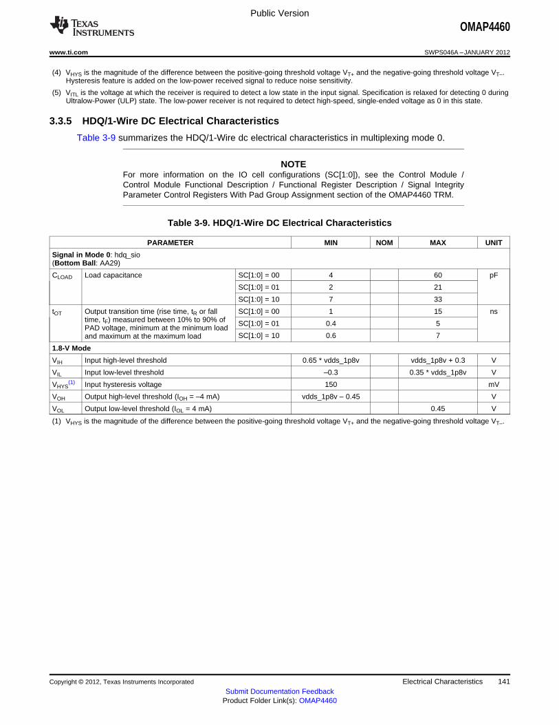
Public Version
OMAP4460
www.ti.com SWPS046A –JANUARY 2012
(4) VHYS is the magnitude of the difference between the positive-going threshold voltage VT+ and the negative-going threshold voltage VT–.Hysteresis feature is added on the low-power received signal to reduce noise sensitivity.
(5) VITL is the voltage at which the receiver is required to detect a low state in the input signal. Specification is relaxed for detecting 0 duringUltralow-Power (ULP) state. The low-power receiver is not required to detect high-speed, single-ended voltage as 0 in this state.
3.3.5 HDQ/1-Wire DC Electrical Characteristics
Table 3-9 summarizes the HDQ/1-Wire dc electrical characteristics in multiplexing mode 0.
NOTEFor more information on the IO cell configurations (SC[1:0]), see the Control Module /Control Module Functional Description / Functional Register Description / Signal IntegrityParameter Control Registers With Pad Group Assignment section of the OMAP4460 TRM.
Table 3-9. HDQ/1-Wire DC Electrical Characteristics
PARAMETER MIN NOM MAX UNIT
Signal in Mode 0: hdq_sio(Bottom Ball: AA29)
CLOAD Load capacitance SC[1:0] = 00 4 60 pF
SC[1:0] = 01 2 21
SC[1:0] = 10 7 33
tOT Output transition time (rise time, tR or fall SC[1:0] = 00 1 15 nstime, tF) measured between 10% to 90% of SC[1:0] = 01 0.4 5PAD voltage, minimum at the minimum load
SC[1:0] = 10 0.6 7and maximum at the maximum load
1.8-V Mode
VIH Input high-level threshold 0.65 * vdds_1p8v vdds_1p8v + 0.3 V
VIL Input low-level threshold –0.3 0.35 * vdds_1p8v V
VHYS(1) Input hysteresis voltage 150 mV
VOH Output high-level threshold (IOH = –4 mA) vdds_1p8v – 0.45 V
VOL Output low-level threshold (IOL = 4 mA) 0.45 V
(1) VHYS is the magnitude of the difference between the positive-going threshold voltage VT+ and the negative-going threshold voltage VT–.
Copyright © 2012, Texas Instruments Incorporated Electrical Characteristics 141Submit Documentation Feedback
Product Folder Link(s): OMAP4460
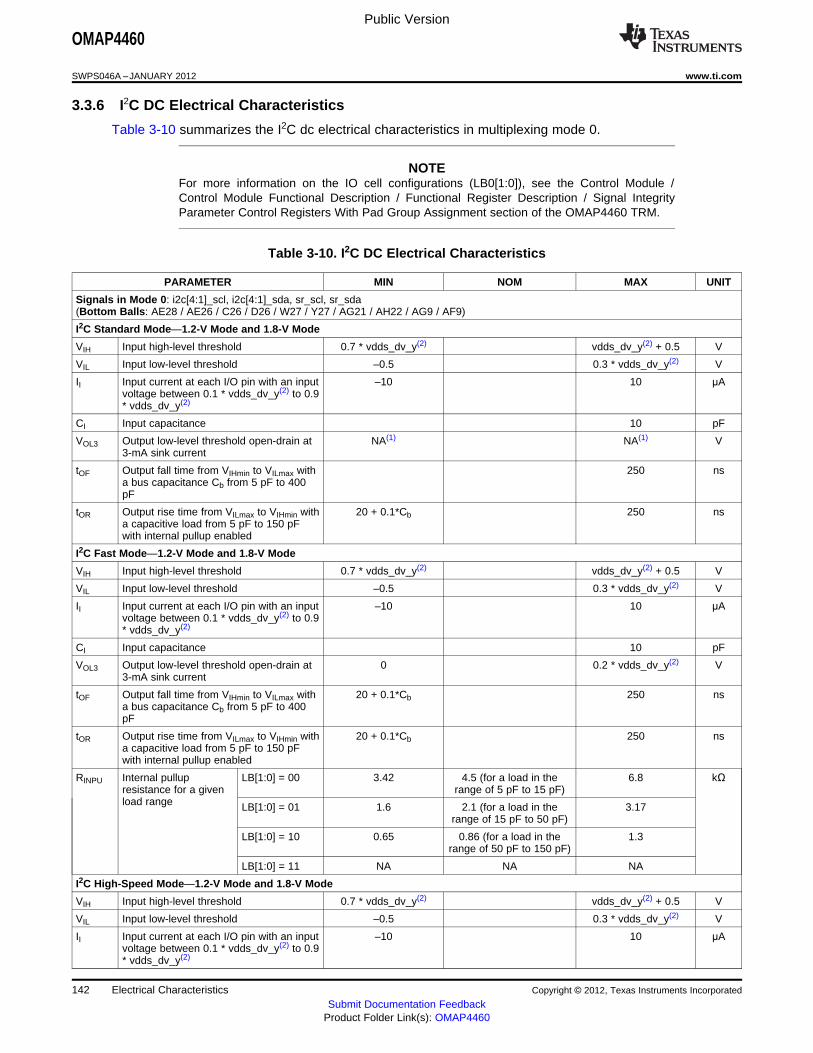
Public Version
OMAP4460
SWPS046A –JANUARY 2012 www.ti.com
3.3.6 I2C DC Electrical Characteristics
Table 3-10 summarizes the I2C dc electrical characteristics in multiplexing mode 0.
NOTEFor more information on the IO cell configurations (LB0[1:0]), see the Control Module /Control Module Functional Description / Functional Register Description / Signal IntegrityParameter Control Registers With Pad Group Assignment section of the OMAP4460 TRM.
Table 3-10. I2C DC Electrical Characteristics
PARAMETER MIN NOM MAX UNIT
Signals in Mode 0: i2c[4:1]_scl, i2c[4:1]_sda, sr_scl, sr_sda(Bottom Balls: AE28 / AE26 / C26 / D26 / W27 / Y27 / AG21 / AH22 / AG9 / AF9)
I2C Standard Mode—1.2-V Mode and 1.8-V Mode
VIH Input high-level threshold 0.7 * vdds_dv_y(2) vdds_dv_y(2) + 0.5 V
VIL Input low-level threshold –0.5 0.3 * vdds_dv_y(2) V
II Input current at each I/O pin with an input –10 10 µAvoltage between 0.1 * vdds_dv_y(2) to 0.9* vdds_dv_y(2)
CI Input capacitance 10 pF
VOL3 Output low-level threshold open-drain at NA(1) NA(1) V3-mA sink current
tOF Output fall time from VIHmin to VILmax with 250 nsa bus capacitance Cb from 5 pF to 400pF
tOR Output rise time from VILmax to VIHmin with 20 + 0.1*Cb 250 nsa capacitive load from 5 pF to 150 pFwith internal pullup enabled
I2C Fast Mode—1.2-V Mode and 1.8-V Mode
VIH Input high-level threshold 0.7 * vdds_dv_y(2) vdds_dv_y(2) + 0.5 V
VIL Input low-level threshold –0.5 0.3 * vdds_dv_y(2) V
II Input current at each I/O pin with an input –10 10 µAvoltage between 0.1 * vdds_dv_y(2) to 0.9* vdds_dv_y(2)
CI Input capacitance 10 pF
VOL3 Output low-level threshold open-drain at 0 0.2 * vdds_dv_y(2) V3-mA sink current
tOF Output fall time from VIHmin to VILmax with 20 + 0.1*Cb 250 nsa bus capacitance Cb from 5 pF to 400pF
tOR Output rise time from VILmax to VIHmin with 20 + 0.1*Cb 250 nsa capacitive load from 5 pF to 150 pFwith internal pullup enabled
RINPU Internal pullup LB[1:0] = 00 3.42 4.5 (for a load in the 6.8 kΩresistance for a given range of 5 pF to 15 pF)load range LB[1:0] = 01 1.6 2.1 (for a load in the 3.17
range of 15 pF to 50 pF)
LB[1:0] = 10 0.65 0.86 (for a load in the 1.3range of 50 pF to 150 pF)
LB[1:0] = 11 NA NA NA
I2C High-Speed Mode—1.2-V Mode and 1.8-V Mode
VIH Input high-level threshold 0.7 * vdds_dv_y(2) vdds_dv_y(2) + 0.5 V
VIL Input low-level threshold –0.5 0.3 * vdds_dv_y(2) V
II Input current at each I/O pin with an input –10 10 µAvoltage between 0.1 * vdds_dv_y(2) to 0.9* vdds_dv_y(2)
142 Electrical Characteristics Copyright © 2012, Texas Instruments Incorporated
Submit Documentation FeedbackProduct Folder Link(s): OMAP4460
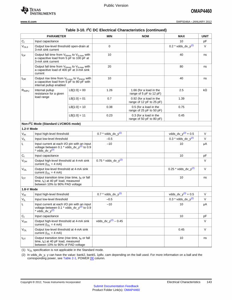
Public Version
OMAP4460
www.ti.com SWPS046A –JANUARY 2012
Table 3-10. I2C DC Electrical Characteristics (continued)
PARAMETER MIN NOM MAX UNIT
CI Input capacitance 10 pF
VOL3 Output low-level threshold open-drain at 0 0.2 * vdds_dv_y(2) V3-mA sink current
tOF Output fall time from VIHmin to VILmax with 10 40 nsa capacitive load from 5 pF to 100 pF at3-mA sink current
Output fall time from VIHmin to VILmax with 20 80 nsa capacitive load of 400 pF at 3-mA sinkcurrent
tOR Output rise time from VILmax to VIHmin with 10 40 nsa capacitive load from 5 pF to 80 pF withinternal pullup enabled
RINPU Internal pullup LB[1:0] = 00 1.26 1.66 (for a load in the 2.5 kΩresistance for a given range of 5 pF to 12 pF)load range LB[1:0] = 01 0.7 0.92 (for a load in the 1.39
range of 12 pF to 25 pF)
LB[1:0] = 10 0.38 0.5 (for a load in the 0.75range of 25 pF to 50 pF)
LB[1:0] = 11 0.23 0.3 (for a load in the 0.45range of 50 pF to 80 pF)
Non-I2C Mode (Standard LVCMOS mode)
1.2-V Mode
VIH Input high-level threshold 0.7 * vdds_dv_y(2) vdds_dv_y(2) + 0.5 V
VIL Input low-level threshold –0.5 0.3 * vdds_dv_y(2) V
II Input current at each I/O pin with an input –10 10 µAvoltage between 0.1 * vdds_dv_y(2) to 0.9* vdds_dv_y(2)
CI Input capacitance 10 pF
VOH Output high-level threshold at 4-mA sink 0.75 * vdds_dv_y(2) Vcurrent (IOL = 4 mA)
VOL Output low-level threshold at 4-mA sink 0.25 * vdds_dv_y(2) Vcurrent (IOL = 4 mA)
tOT Output transition time (rise time, tR or fall 10 nstime, tF) at 40 pF load, measuredbetween 10% to 90% PAD voltage
1.8-V Mode
VIH Input high-level threshold 0.7 * vdds_dv_y(2) vdds_dv_y(2) + 0.5 V
VIL Input low-level threshold –0.5 0.3 * vdds_dv_y(2) V
II Input current at each I/O pin with an input –10 10 µAvoltage between 0.1 * vdds_dv_y(2) to 0.9* vdds_dv_y(2)
CI Input capacitance 10 pF
VOH Output high-level threshold at 4-mA sink vdds_dv_y(2) – 0.45 Vcurrent (IOL = 4 mA)
VOL Output low-level threshold at 4-mA sink 0.45 Vcurrent (IOL = 4 mA)
tOT Output transition time (rise time, tR or fall 10 nstime, tF) at 40 pF load, measuredbetween 10% to 90% of PAD voltage
(1) VOL specification is not applicable in the Standard mode.
(2) In vdds_dv_y, y can have the value: bank2, bank5, 1p8v, cam depending on the ball used. For more information on a ball and thecorresponding power, see Table 2-1, POWER [9] column.
Copyright © 2012, Texas Instruments Incorporated Electrical Characteristics 143Submit Documentation Feedback
Product Folder Link(s): OMAP4460

Public Version
OMAP4460
SWPS046A –JANUARY 2012 www.ti.com
3.3.7 Audio McBSP / PDM / DMIC DC Electrical Characteristics
Table 3-11 summarizes the audio McBSP / PDM / DMIC dc electrical characteristics in multiplexing mode0.
NOTEFor more information on the IO cell configurations (MB[1:0] and LB0, SC[1:0]), see theControl Module / Control Module Functional Description / Functional Register Description /Signal Integrity Parameter Control Registers With Pad Group Assignment section of theOMAP4460 TRM.
Table 3-11. Audio McBSP / PDM / DMIC DC Electrical Characteristics
PARAMETER MIN NOM MAX UNIT
Signals in Mode 0: abe_mcbsp2_clkx, abe_mcbsp2_dr, abe_mcbsp2_dx, abe_mcbsp2_fsx, abe_mcbsp1_clkx, abe_mcbsp1_dr,abe_mcbsp1_dx, abe_mcbsp1_fsx, abe_pdm_ul_data, abe_pdm_dl_data, abe_pdm_frame, abe_pdm_lb_clk, abe_dmic_clk1,abe_dmic_din[3:1](Bottom Balls: AD27 / AD26 / AD25 / AC28 / AC26 / AC25 / AB25 / AC27 / AG25 / AF25 / AE25 / AF26 / AE24 / AF24 / AG24 / AH24)
CLOAD(4) Load capacitance MB[1:0] = 11 LB0 = 1 (Mode1) 20 25 pF
maximum frequency = 24 MHztransmission line delay = 670 ps
MB[1:0] = 11 LB0 = 1 (Mode1) 2 5maximum frequency = 60 MHztransmission line delay = 335 ps
MB[1:0] = 01 LB0 = 0 (Mode2) 14 17maximum frequency = 25 MHztransmission line delay = 335 ps
MB[1:0] = 01 LB0 = 0 (Mode2) 2 5maximum frequency = 48 MHztransmission line delay = 536 ps
MB[1:0] = 10 LB0 = 1 (Mode3) 23 28maximum frequency = 20 MHztransmission line delay = 838 ps
MB[1:0] = 10 LB0 = 1 (Mode3) 16 20maximum frequency = 24 MHztransmission line delay = 670 ps
MB[1:0] = 10 LB0 = 0 (Mode4) 16 20maximum frequency = 4 MHztransmission line delay = 1675 ps
MB[1:0] = 10 LB0 = 0 (Mode4) 2 5maximum frequency = 25 MHztransmission line delay = 670 ps
MB[1:0] = 10 LB0 = 0 (Mode4) 5 7maximum frequency = 25 MHztransmission line delay = 670 ps
MB[1:0] = 10 LB0 = 0 (Mode4) 2 11maximum frequency = 25 MHztransmission line delay = 536 ps
144 Electrical Characteristics Copyright © 2012, Texas Instruments Incorporated
Submit Documentation FeedbackProduct Folder Link(s): OMAP4460

Public Version
OMAP4460
www.ti.com SWPS046A –JANUARY 2012
Table 3-11. Audio McBSP / PDM / DMIC DC Electrical Characteristics (continued)
PARAMETER MIN NOM MAX UNIT
tOT(4) Output transition time MB[1:0] = 11 LB0 = 1 (Mode1) 10 ns
(rise time, tR or fall maximum frequency = 24 MHztime, tF) measured transmission line delay = 670 psbetween 10% to 90% of MB[1:0] = 11 LB0 = 1 (Mode1) 4PAD voltage, the maximum frequency = 60 MHzmaximum at maximum transmission line delay = 335 psload
MB[1:0] = 01 LB0 = 0 (Mode2) 5.6(1)
maximum frequency = 25 MHztransmission line delay = 335 ps
MB[1:0] = 01 LB0 = 0 (Mode2) 6.3maximum frequency = 48 MHztransmission line delay = 536 ps
MB[1:0] = 10 LB0 = 1 (Mode3) 10.5(1)
maximum frequency = 20 MHztransmission line delay = 838 ps
MB[1:0] = 10 LB0 = 1 (Mode3) 12.5maximum frequency = 24 MHztransmission line delay = 670 ps
MB[1:0] = 10 LB0 = 0 (Mode4) 16.8(1)
maximum frequency = 4 MHztransmission line delay = 1675 ps
MB[1:0] = 10 LB0 = 0 (Mode4) 10maximum frequency = 25 MHztransmission line delay = 670 ps
MB[1:0] = 10 LB0 = 0 (Mode4) 12.2maximum frequency = 25 MHztransmission line delay = 670 ps
MB[1:0] = 10 LB0 = 0 (Mode4) 8(1)
maximum frequency = 25 MHztransmission line delay = 536 ps
1.2-V Mode
VIH Input high-level threshold 0.65 * vdds_dv_y(2) vdds_dv_y(2) + 0.3 V
VIL Input low-level threshold –0.3 0.35 * vdds_dv_y(2) V
VHYS(3) Input hysteresis voltage 135 mV
VOH Output high-level threshold (IOH = 4 mA) 0.75 * vdds_dv_y(2) V
VOL Output low-level threshold (IOL = 4 mA) 0.25 * vdds_dv_y(2) V
1.8-V Mode
VIH Input high-level threshold 0.65 * vdds_dv_y(2) vdds_dv_y(2) + 0.3 V
VIL Input low-level threshold –0.3 0.35 * vdds_dv_y(2) V
VHYS(3) Input hysteresis voltage 150 mV
VOH Output high-level threshold (IOH = 4 mA) vdds_dv_y(2) – 0.45 V
VOL Output low-level threshold (IOL = 4 mA) 0.45 V
Signal in Mode 0: abe_clks(Bottom Ball: AH26)
CLOAD Load capacitance SC[1:0] = 00 4 60 pF
SC[1:0] = 01 2 21
SC[1:0] = 10 7 33
tOT Output transition time (rise time, tR or fall SC[1:0] = 00 1 15 nstime, tF) measured between 10% to 90% of SC[1:0] = 01 0.4 5PAD voltage, minimum at the minimum load
SC[1:0] = 10 0.6 7and maximum at the maximum load
1.2-V Mode
VIH Input high-level threshold 0.65 * vdds_dv_bank2 vdds_dv_bank2 + 0.3 V
VIL Input low-level threshold –0.3 0.35 * vdds_dv_bank2 V
VHYS(3) Input hysteresis voltage 135 mV
Copyright © 2012, Texas Instruments Incorporated Electrical Characteristics 145Submit Documentation Feedback
Product Folder Link(s): OMAP4460

Public Version
OMAP4460
SWPS046A –JANUARY 2012 www.ti.com
Table 3-11. Audio McBSP / PDM / DMIC DC Electrical Characteristics (continued)
PARAMETER MIN NOM MAX UNIT
VOH Output high-level threshold (IOH = –4 mA) 0.75 * vdds_dv_bank2 V
VOL Output low-level threshold (IOL = 4 mA) 0.25 * vdds_dv_bank2 V
1.8-V Mode
VIH Input high-level threshold 0.65 * vdds_dv_bank2 vdds_dv_bank2 + 0.3 V
VIL Input low-level threshold –0.3 0.35 * vdds_dv_bank2 V
VHYS(3) Input hysteresis voltage 150 mV
VOH Output high-level threshold (IOH = –4 mA) vdds_dv_bank2 – 0.45 V
VOL Output low-level threshold (IOL = 4 mA) 0.45 V
(1) Output transition time measured between 20% to 80% of PAD voltage.
(2) In vdds_dv_y, y can have the value: bank1 or bank2 depending on the ball used. For more information on a ball and the correspondingpower, see Table 2-1, POWER [9] column.
(3) VHYS is the magnitude of the difference between the positive-going threshold voltage VT+ and the negative-going threshold voltage VT–.
(4) Depending on the programming mode, different output load and transition time are available following the targeted maximum frequency,transmission line or output transition time.
3.3.8 McSPI DC Electrical Characteristics
Table 3-12 summarizes the McSPI dc electrical characteristics in multiplexing mode 0.
NOTEFor more information on the IO cell configurations (MB[1:0] and LB0, SC[1:0]), see theControl Module / Control Module Functional Description / Functional Register Description /Signal Integrity Parameter Control Registers With Pad Group Assignment section of theOMAP4460 TRM.
Table 3-12. McSPI DC Electrical Characteristics
PARAMETER MIN NOM MAX UNIT
Signals in Mode 0: mcspi1_clk, mcspi1_somi, mcspi1_simo, mcspi1_cs[1:0](Bottom Balls: AF22 / AE22 / AG22 / AE23 / AF23)
CLOAD Load capacitance SC[1:0] = 00 4 60 pF
SC[1:0] = 01 2 21
SC[1:0] = 10 7 33
tOT Output transition time (rise time, tR or fall SC[1:0] = 00 1 15 nstime, tF) measured between 10% to 90% SC[1:0] = 01 0.4 5of PAD voltage, minimum at the
SC[1:0] = 10 0.6 7minimum load and maximum at themaximum load
1.2-V Mode
VIH Input high-level threshold 0.65 * vdds_dv_bank3 vdds_dv_bank3 + 0.3 V
VIL Input low-level threshold –0.3 0.35 * vdds_dv_bank3 V
VHYS(3) Input hysteresis voltage 135 mV
VOH Output high-level threshold (IOH = –4 mA) 0.75 * vdds_dv_bank3 V
VOL Output low-level threshold (IOL = 4 mA) 0.25 * vdds_dv_bank3 V
1.8-V Mode
VIH Input high-level threshold 0.65 * vdds_dv_bank3 vdds_dv_bank3 + 0.3 V
VIL Input low-level threshold –0.3 0.35 * vdds_dv_bank3 V
VHYS(3) Input hysteresis voltage 150 mV
VOH Output high-level threshold (IOH = –4 mA) vdds_dv_bank3 – 0.45 V
VOL Output low-level threshold (IOL = 4 mA) 0.45 V
146 Electrical Characteristics Copyright © 2012, Texas Instruments Incorporated
Submit Documentation FeedbackProduct Folder Link(s): OMAP4460
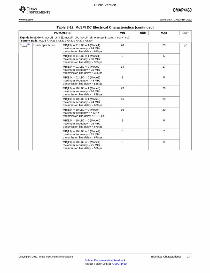
Public Version
OMAP4460
www.ti.com SWPS046A –JANUARY 2012
Table 3-12. McSPI DC Electrical Characteristics (continued)
PARAMETER MIN NOM MAX UNIT
Signals in Mode 0: mcspi1_cs[3:2], mcspi4_clk, mcspi4_simo, mcspi4_somi, mcspi4_cs0(Bottom Balls: AG23 / AH23 / AE21 / AF20 / AF21 / AE20)
CLOAD(4) Load capacitance MB[1:0] = 11 LB0 = 1 (Mode1) 20 25 pF
maximum frequency = 24 MHztransmission line delay = 670 ps
MB[1:0] = 11 LB0 = 1 (Mode1) 2 5maximum frequency = 60 MHztransmission line delay = 335 ps
MB[1:0] = 01 LB0 = 0 (Mode2) 14 17maximum frequency = 25 MHztransmission line delay = 335 ps
MB[1:0] = 01 LB0 = 0 (Mode2) 2 5maximum frequency = 48 MHztransmission line delay = 536 ps
MB[1:0] = 10 LB0 = 1 (Mode3) 23 28maximum frequency = 20 MHztransmission line delay = 838 ps
MB[1:0] = 10 LB0 = 1 (Mode3) 16 20maximum frequency = 24 MHztransmission line delay = 670 ps
MB[1:0] = 10 LB0 = 0 (Mode4) 16 20maximum frequency = 4 MHztransmission line delay = 1675 ps
MB[1:0] = 10 LB0 = 0 (Mode4) 2 5maximum frequency = 25 MHztransmission line delay = 670 ps
MB[1:0] = 10 LB0 = 0 (Mode4) 5 7maximum frequency = 25 MHztransmission line delay = 670 ps
MB[1:0] = 10 LB0 = 0 (Mode4) 2 11maximum frequency = 25 MHztransmission line delay = 536 ps
Copyright © 2012, Texas Instruments Incorporated Electrical Characteristics 147Submit Documentation Feedback
Product Folder Link(s): OMAP4460
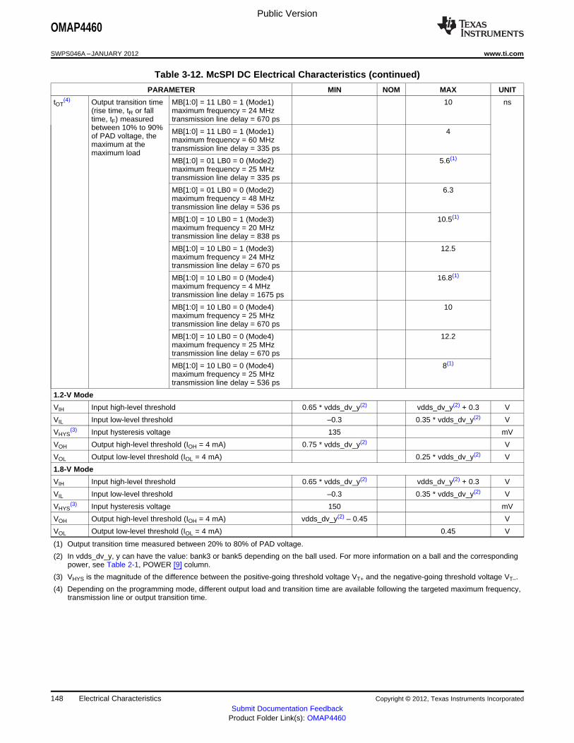
Public Version
OMAP4460
SWPS046A –JANUARY 2012 www.ti.com
Table 3-12. McSPI DC Electrical Characteristics (continued)
PARAMETER MIN NOM MAX UNIT
tOT(4) Output transition time MB[1:0] = 11 LB0 = 1 (Mode1) 10 ns
(rise time, tR or fall maximum frequency = 24 MHztime, tF) measured transmission line delay = 670 psbetween 10% to 90% MB[1:0] = 11 LB0 = 1 (Mode1) 4of PAD voltage, the maximum frequency = 60 MHzmaximum at the transmission line delay = 335 psmaximum load
MB[1:0] = 01 LB0 = 0 (Mode2) 5.6(1)
maximum frequency = 25 MHztransmission line delay = 335 ps
MB[1:0] = 01 LB0 = 0 (Mode2) 6.3maximum frequency = 48 MHztransmission line delay = 536 ps
MB[1:0] = 10 LB0 = 1 (Mode3) 10.5(1)
maximum frequency = 20 MHztransmission line delay = 838 ps
MB[1:0] = 10 LB0 = 1 (Mode3) 12.5maximum frequency = 24 MHztransmission line delay = 670 ps
MB[1:0] = 10 LB0 = 0 (Mode4) 16.8(1)
maximum frequency = 4 MHztransmission line delay = 1675 ps
MB[1:0] = 10 LB0 = 0 (Mode4) 10maximum frequency = 25 MHztransmission line delay = 670 ps
MB[1:0] = 10 LB0 = 0 (Mode4) 12.2maximum frequency = 25 MHztransmission line delay = 670 ps
MB[1:0] = 10 LB0 = 0 (Mode4) 8(1)
maximum frequency = 25 MHztransmission line delay = 536 ps
1.2-V Mode
VIH Input high-level threshold 0.65 * vdds_dv_y(2) vdds_dv_y(2) + 0.3 V
VIL Input low-level threshold –0.3 0.35 * vdds_dv_y(2) V
VHYS(3) Input hysteresis voltage 135 mV
VOH Output high-level threshold (IOH = 4 mA) 0.75 * vdds_dv_y(2) V
VOL Output low-level threshold (IOL = 4 mA) 0.25 * vdds_dv_y(2) V
1.8-V Mode
VIH Input high-level threshold 0.65 * vdds_dv_y(2) vdds_dv_y(2) + 0.3 V
VIL Input low-level threshold –0.3 0.35 * vdds_dv_y(2) V
VHYS(3) Input hysteresis voltage 150 mV
VOH Output high-level threshold (IOH = 4 mA) vdds_dv_y(2) – 0.45 V
VOL Output low-level threshold (IOL = 4 mA) 0.45 V
(1) Output transition time measured between 20% to 80% of PAD voltage.
(2) In vdds_dv_y, y can have the value: bank3 or bank5 depending on the ball used. For more information on a ball and the correspondingpower, see Table 2-1, POWER [9] column.
(3) VHYS is the magnitude of the difference between the positive-going threshold voltage VT+ and the negative-going threshold voltage VT–.
(4) Depending on the programming mode, different output load and transition time are available following the targeted maximum frequency,transmission line or output transition time.
148 Electrical Characteristics Copyright © 2012, Texas Instruments Incorporated
Submit Documentation FeedbackProduct Folder Link(s): OMAP4460

Public Version
OMAP4460
www.ti.com SWPS046A –JANUARY 2012
3.3.9 UART DC Electrical Characteristics
Table 3-13 summarizes the UART dc electrical characteristics in multiplexing mode 0.
NOTEFor more information on the IO cell configurations (MB[1:0] and LB0, SC[1:0]), see theControl Module / Control Module Functional Description / Functional Register Description /Signal Integrity Parameter Control Registers With Pad Group Assignment section of theOMAP4460 TRM.
Table 3-13. UART DC Electrical Characteristics
PARAMETER MIN NOM MAX UNIT
Signals in Mode 0: uart3_cts_rctx, uart3_rts_sd, uart3_rx_irrx, uart3_tx_irtx(Bottom Balls: F27 / F28 / G27 / G28)
CLOAD Load capacitance SC[1:0] = 00 4 60 pF
SC[1:0] = 01 2 21
SC[1:0] = 10 7 33
tOT Output transition time (rise time, tR or SC[1:0] = 00 1 15 nsfall time, tF) measured between 10% SC[1:0] = 01 0.4 5to 90% of PAD voltage, minimum at
SC[1:0] = 10 0.6 7the minimum load and maximum atthe maximum load
1.8-V Mode
VIH Input high-level threshold 0.65 * vdds_1p8v vdds_1p8v + 0.3 V
VIL Input low-level threshold –0.3 0.35 * vdds_1p8v V
VHYS(3) Input hysteresis voltage 150 mV
VOH Output high-level threshold (IOH = –4 mA) vdds_1p8v – 0.45 V
VOL Output low-level threshold (IOL = 4 mA) 0.45 V
Copyright © 2012, Texas Instruments Incorporated Electrical Characteristics 149Submit Documentation Feedback
Product Folder Link(s): OMAP4460
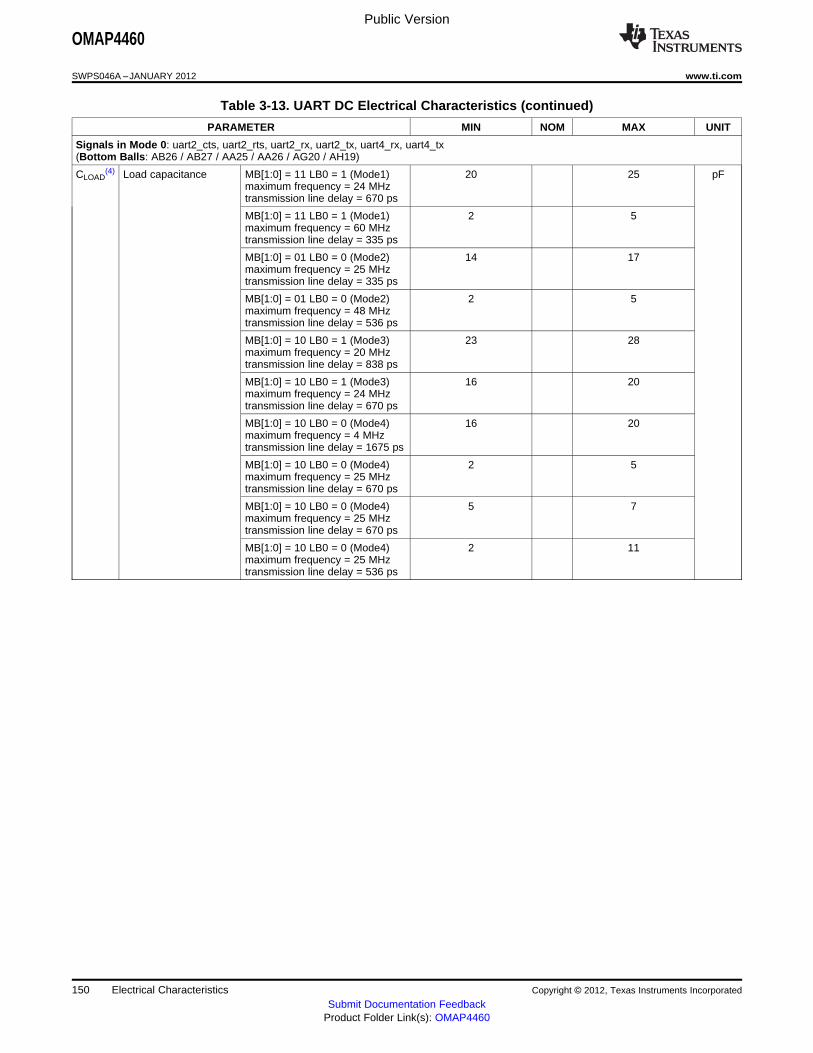
Public Version
OMAP4460
SWPS046A –JANUARY 2012 www.ti.com
Table 3-13. UART DC Electrical Characteristics (continued)
PARAMETER MIN NOM MAX UNIT
Signals in Mode 0: uart2_cts, uart2_rts, uart2_rx, uart2_tx, uart4_rx, uart4_tx(Bottom Balls: AB26 / AB27 / AA25 / AA26 / AG20 / AH19)
CLOAD(4) Load capacitance MB[1:0] = 11 LB0 = 1 (Mode1) 20 25 pF
maximum frequency = 24 MHztransmission line delay = 670 ps
MB[1:0] = 11 LB0 = 1 (Mode1) 2 5maximum frequency = 60 MHztransmission line delay = 335 ps
MB[1:0] = 01 LB0 = 0 (Mode2) 14 17maximum frequency = 25 MHztransmission line delay = 335 ps
MB[1:0] = 01 LB0 = 0 (Mode2) 2 5maximum frequency = 48 MHztransmission line delay = 536 ps
MB[1:0] = 10 LB0 = 1 (Mode3) 23 28maximum frequency = 20 MHztransmission line delay = 838 ps
MB[1:0] = 10 LB0 = 1 (Mode3) 16 20maximum frequency = 24 MHztransmission line delay = 670 ps
MB[1:0] = 10 LB0 = 0 (Mode4) 16 20maximum frequency = 4 MHztransmission line delay = 1675 ps
MB[1:0] = 10 LB0 = 0 (Mode4) 2 5maximum frequency = 25 MHztransmission line delay = 670 ps
MB[1:0] = 10 LB0 = 0 (Mode4) 5 7maximum frequency = 25 MHztransmission line delay = 670 ps
MB[1:0] = 10 LB0 = 0 (Mode4) 2 11maximum frequency = 25 MHztransmission line delay = 536 ps
150 Electrical Characteristics Copyright © 2012, Texas Instruments Incorporated
Submit Documentation FeedbackProduct Folder Link(s): OMAP4460

Public Version
OMAP4460
www.ti.com SWPS046A –JANUARY 2012
Table 3-13. UART DC Electrical Characteristics (continued)
PARAMETER MIN NOM MAX UNIT
tOT(4) Output transition time MB[1:0] = 11 LB0 = 1 (Mode1) 10 ns
(rise time, tR or fall maximum frequency = 24 MHztime, tF) measured transmission line delay = 670 psbetween 10% to 90% of MB[1:0] = 11 LB0 = 1 (Mode1) 4PAD voltage, the maximum frequency = 60 MHzmaximum at the transmission line delay = 335 psmaximum load
MB[1:0] = 01 LB0 = 0 (Mode2) 5.6(1)
maximum frequency = 25 MHztransmission line delay = 335 ps
MB[1:0] = 01 LB0 = 0 (Mode2) 6.3maximum frequency = 48 MHztransmission line delay = 536 ps
MB[1:0] = 10 LB0 = 1 (Mode3) 10.5(1)
maximum frequency = 20 MHztransmission line delay = 838 ps
MB[1:0] = 10 LB0 = 1 (Mode3) 12.5maximum frequency = 24 MHztransmission line delay = 670 ps
MB[1:0] = 10 LB0 = 0 (Mode4) 16.8(1)
maximum frequency = 4 MHztransmission line delay = 1675 ps
MB[1:0] = 10 LB0 = 0 (Mode4) 10maximum frequency = 25 MHztransmission line delay = 670 ps
MB[1:0] = 10 LB0 = 0 (Mode4) 12.2maximum frequency = 25 MHztransmission line delay = 670 ps
MB[1:0] = 10 LB0 = 0 (Mode4) 8(1)
maximum frequency = 25 MHztransmission line delay = 536 ps
1.2-V Mode
VIH Input high-level threshold 0.65 * vdds_dv_y(2) vdds_dv_y(2) + 0.3 V
VIL Input low-level threshold –0.3 0.35 * vdds_dv_y(2) V
VHYS(3) Input hysteresis voltage 135 mV
VOH Output high-level threshold (IOH = 2 mA)(6) 0.75 * vdds_dv_y(2) V
VOL Output low-level threshold (IOL = 2 mA)(6) 0.25 * vdds_dv_y(2) V
1.8-V Mode
VIH Input high-level threshold 0.65 * vdds_dv_y(2) vdds_dv_y(2) + 0.3 V
VIL Input low-level threshold –0.3 0.35 * vdds_dv_y(2) V
VHYS(3) Input hysteresis voltage 150 mV
VOH Output high-level threshold (IOH = 2 mA)(6) vdds_dv_y(2) – 0.45(5) V
VOL Output low-level threshold (IOL = 2 mA)(6) 0.45(5) V
(1) Output transition time measured between 20% to 80% of PAD voltage.
(2) In vdds_dv_y, y can have the value: bank1 or bank5 depending on the ball used. For more information on a ball and the correspondingpower, see Table 2-1, POWER [9] column.
(3) VHYS is the magnitude of the difference between the positive-going threshold voltage VT+ and the negative-going threshold voltage VT–.
(4) Depending on the programming mode, different output load and transition time are available following the targeted maximum frequency,transmission line or output transition time.
(5) For uart4_rx ball (AG20) and uart4_tx ball (AH19):VOH = vdds_dv_y – 0.3 V and VOL = 0.3 V for IOH = 1 mAVOH = vdds_dv_y – 0.2 V and VOL = 0.2 V for IOL = 250 µA
(6) This IO buffer supports up to 4 mA of drive strength. For this drive strength, the VOL/VOH described in the table above are not assured.
Copyright © 2012, Texas Instruments Incorporated Electrical Characteristics 151Submit Documentation Feedback
Product Folder Link(s): OMAP4460

Public Version
OMAP4460
SWPS046A –JANUARY 2012 www.ti.com
3.3.10 USB DC Electrical Characteristics
Table 3-14 summarizes the USB dc electrical characteristics in multiplexing mode 0.
NOTEFor more information on the IO cell configurations (DS0, MB[1:0], i[2:0], sr[1:0],SPEEDCTRL), see the Control Module / Control Module Functional Description / FunctionalRegister Description / Signal Integrity Parameter Control Registers With Pad GroupAssignment section of the OMAP4460 TRM.
Table 3-14. USB DC Electrical Characteristics
PARAMETER MIN NOM MAX UNIT
Signals in Mode 0: usbb1_ulpitll_clk, usbb2_ulpitll_clk(Bottom Balls: AE18 / AG12)
CLOAD Load capacitance DS0 = 0 (Mode2) 5 35 pFmaximum frequency = 20 MHztransmission line delay = 1340 ps
DS0 = 0 (Mode2) 2 5maximum frequency = 48 MHztransmission line delay = 670 ps
DS0 = 0 (Mode2) 2 5maximum frequency = 60 MHztransmission line delay = 335 ps
DS0 = 0 (Mode2) 2 5maximum frequency = 75 MHztransmission line delay = 402 ps
DS0 = 1 (Mode1) 2 5maximum frequency = 100 MHztransmission line delay = 203 ps
tOT Output transition DS0 = 0 (Mode2) 15(1) nstime (rise time, tR maximum frequency = 20 MHzor fall time, tF), the transmission line delay = 1340 psmaximum at the DS0 = 0 (Mode2) 3(1)maximum load maximum frequency = 48 MHz
transmission line delay = 670 ps
DS0 = 0 (Mode2) 3(2)
maximum frequency = 60 MHztransmission line delay = 335 ps
DS0 = 0 (Mode2) 4(3)
maximum frequency = 75 MHztransmission line delay = 402 ps
DS0 = 1 (Mode1) 2(3)
maximum frequency = 100 MHztransmission line delay = 203 ps
1.2-V Mode
VIH Input high-level threshold 0.65 * vdds_dv_y(4) vdds_dv_y(4) + 0.3 V
VIL Input low-level threshold –0.3 0.35 * vdds_dv_y(4) V
VHYS(11) Input hysteresis voltage 60 mV
VOH Output high-level threshold (IOH = 4 mA for 50Ω mode, 0.75 * vdds_dv_y(4) VIOH = 8 mA for 25Ω mode)
VOL Output low-level threshold (IOL = 4 mA for 50Ω mode, 0.25 * vdds_dv_y(4) VIOL = 8 mA for 25Ω mode)
1.8-V Mode
VIH Input high-level threshold 0.65 * vdds_dv_y(4) vdds_dv_y(4) + 0.3 V
VIL Input low-level threshold –0.3 0.35 * vdds_dv_y(4) V
VHYS(11) Input hysteresis voltage 70 mV
152 Electrical Characteristics Copyright © 2012, Texas Instruments Incorporated
Submit Documentation FeedbackProduct Folder Link(s): OMAP4460
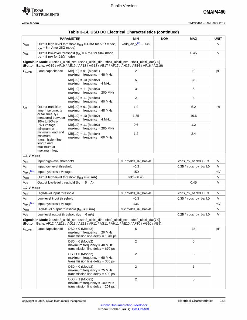
Public Version
OMAP4460
www.ti.com SWPS046A –JANUARY 2012
Table 3-14. USB DC Electrical Characteristics (continued)
PARAMETER MIN NOM MAX UNIT
VOH Output high-level threshold (IOH = 4 mA for 50Ω mode, vdds_dv_y(4) – 0.45 VIOH = 8 mA for 25Ω mode)
VOL Output low-level threshold (IOL = 4 mA for 50Ω mode, 0.45 VIOL = 8 mA for 25Ω mode)
Signals in Mode 0: usbb1_ulpitll_stp, usbb1_ulpitll_dir, usbb1_ulpitll_nxt, usbb1_ulpitll_dat[7:0](Bottom Balls: AG19 / AF19 / AE19 / AF18 / AG18 / AE17 / AF17 / AH17 / AE16 / AF16 / AG16)
CLOAD Load capacitance MB[1:0] = 01 (Mode1) 2 10 pFmaximum frequency = 48 MHz
MB[1:0] = 10 (Mode2) 5 35maximum frequency = 4 MHz
MB[1:0] = 11 (Mode3) 3 5maximum frequency = 200 MHz
MB[1:0] = 11 (Mode4) 2 5maximum frequency = 60 MHz
tOT Output transition MB[1:0] = 01 (Mode1) 1.2 5.2 nstime (rise time, tR maximum frequency = 48 MHzor fall time, tF) MB[1:0] = 10 (Mode2) 1.35 10.6measured between maximum frequency = 4 MHz10% to 90% of
MB[1:0] = 11 (Mode3) 0.6 1.2PAD voltage,maximum frequency = 200 MHzminimum at
minimum load and MB[1:0] = 11 (Mode4) 1.2 3.4minimum maximum frequency = 60 MHztransmission linelength andmaximum atmaximum load
1.8-V Mode
VIH Input high-level threshold 0.65*vdds_dv_bank0 vdds_dv_bank0 + 0.3 V
VIL Input low-level threshold –0.3 0.35 * vdds_dv_bank0 V
VHYS(11) Input hysteresis voltage 150 mV
VOH Output high-level threshold (IOH = –6 mA) vdd – 0.45 V
VOL Output low-level threshold (IOL = 6 mA) 0.45 V
1.2-V Mode
VIH High-level input threshold 0.65*vdds_dv_bank0 vdds_dv_bank0 + 0.3 V
VIL Low-level input threshold –0.3 0.35 * vdds_dv_bank0 V
VHYS(11) Input hysteresis voltage 135 mV
VOH High-level output threshold (IOH = 6 mA) 0.75*vdds_dv_bank0 V
VOL Low-level output threshold (IOL = 6 mA) 0.25 * vdds_dv_bank0 V
Signals in Mode 0: usbb2_ulpitll_stp, usbb2_ulpitll_dir, usbb2_ulpitll_nxt, usbb2_ulpitll_dat[7:0](Bottom Balls: AF12 / AE12 / AG13 / AE11 / AF11 / AG11 / AH11 / AE10 / AF10 / AG10 / AE9)
CLOAD Load capacitance DS0 = 0 (Mode2) 5 35 pFmaximum frequency = 20 MHztransmission line delay = 1340 ps
DS0 = 0 (Mode2) 2 5maximum frequency = 48 MHztransmission line delay = 670 ps
DS0 = 0 (Mode2) 2 5maximum frequency = 60 MHztransmission line delay = 335 ps
DS0 = 0 (Mode2) 2 5maximum frequency = 75 MHztransmission line delay = 402 ps
DS0 = 1 (Mode1) 2 5maximum frequency = 100 MHztransmission line delay = 203 ps
Copyright © 2012, Texas Instruments Incorporated Electrical Characteristics 153Submit Documentation Feedback
Product Folder Link(s): OMAP4460
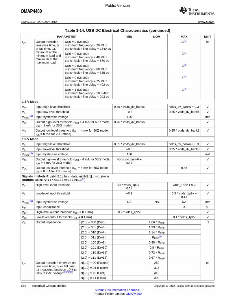
Public Version
OMAP4460
SWPS046A –JANUARY 2012 www.ti.com
Table 3-14. USB DC Electrical Characteristics (continued)
PARAMETER MIN NOM MAX UNIT
tOT Output transition DS0 = 0 (Mode2) 15(1) nstime (rise time, tR maximum frequency = 20 MHzor fall time, tF), transmission line delay = 1340 psminimum at the DS0 = 0 (Mode2) 3(1)minimum load and maximum frequency = 48 MHzmaximum at the transmission line delay = 670 psmaximum load
DS0 = 0 (Mode2) 3(2)
maximum frequency = 60 MHztransmission line delay = 335 ps
DS0 = 0 (Mode2) 4(3)
maximum frequency = 75 MHztransmission line delay = 402 ps
DS0 = 1 (Mode1) 2(3)
maximum frequency = 100 MHztransmission line delay = 203 ps
1.2-V Mode
VIH Input high-level threshold 0.65 * vdds_dv_bank6 vdds_dv_bank6 + 0.3 V
VIL Input low-level threshold –0.3 0.35 * vdds_dv_bank6 V
VHYS(11) Input hysteresis voltage 135 mV
VOH Output high-level threshold (IOH = 4 mA for 50Ω mode, 0.75 * vdds_dv_bank6 VIOH = 8 mA for 25Ω mode)
VOL Output low-level threshold (IOL = 4 mA for 50Ω mode, 0.25 * vdds_dv_bank6 VIOL = 8 mA for 25Ω mode)
1.8-V Mode
VIH Input high-level threshold 0.65 * vdds_dv_bank6 vdds_dv_bank6 + 0.3 V
VIL Input low-level threshold –0.3 0.35 * vdds_dv_bank6 V
VHYS(11) Input hysteresis voltage 150 mV
VOH Output high-level threshold (IOH = 4 mA for 50Ω mode, vdds_dv_bank6 – VIOH = 8 mA for 25Ω mode) 0.45
VOL Output low-level threshold (IOL = 4 mA for 50Ω mode, 0.45 VIOL = 8 mA for 25Ω mode)
Signals in Mode 0: usbb[2:1]_hsic_data, usbb[2:1]_hsic_strobe(Bottom Balls: AF14 / AE14 / AF13 / AE13(5))
VIH High-level input threshold 0.5 * vdds_1p2v + vdds_1p2v + 0.2 V0.13
VIL Low-level input threshold –0.2 0.5 * vdds_1p2v – V0.13
VHYS(11) Input hysteresis voltage NA NA NA mV
CIN Input capacitance 3 pF
VOH High-level output threshold (IOH = 0.1 mA) 0.9 * vdds_1p2v V
VOL Low-level output threshold (IOL = 0.1 mA) 0.1 * vdds_1p2v V
ZO Output impedance i[2:0] = 000 (Drv5) 1.66 * RREF Ωi[2:0] = 001 (Drv6) 1.33 * RREF
i[2:0] = 010 (Drv7) 1.14 * RREF
i[2:0] = 011 (Drv8) RREF(6)
i[2:0] = 100 (Drv9) 0.88 * RREF
i[2:0] = 101 (Drv10) 0.8 * RREF
i[2:0] = 110 (Drv11) 0.73 * RREF
i[2:0] = 111 (Drv12) 0.67 * RREF
tOT Output transition time/turn-on sr[1:0] = 00 (Fastest) 250 pstime (rise time, tR or fall time, sr[1:0] = 01 (Faster) 315tF) measured between 10% to
sr[1:0] = 10 (Fast) 34090% of PAD voltage(7)(8)(10)
sr[1:0] = 11 (Slow) 390
154 Electrical Characteristics Copyright © 2012, Texas Instruments Incorporated
Submit Documentation FeedbackProduct Folder Link(s): OMAP4460

Public Version
OMAP4460
www.ti.com SWPS046A –JANUARY 2012
Table 3-14. USB DC Electrical Characteristics (continued)
PARAMETER MIN NOM MAX UNIT
Maximum noise on the IO sr[1:0] = 00 (Fastest) 215 mVPPsupply voltage(7)(9)(10)
sr[1:0] = 01 (Faster) 110
sr[1:0] = 10 (Fast) 108
sr[1:0] = 11 (Slow) 110
Signal in Mode 0: usba0_otg_ce(Bottom Ball: C3)
USB Low-Speed / Full-Speed Differential Transmitter
VOH Output high-level threshold (Pulldown R = 15kΩ on 2.8 3.3 3.6 Vboth DP and DM)
VOL Output low-level threshold (Pullup R = 1.5kΩ @3.6V on 0 0.1 0.3 Vboth DP and DM)
ZDRV Driver output resistance 28 45 49.5 ΩtLSOT Output transition time (rise time, tR or fall time, tF), 75 300 ns
measured between 10% to 90% of PAD voltage, CL =200 to 600 pF on both DP and DM, pullup R = 1.5kΩ@3.6V for DM only
tFSOT Output transition time (rise time, tR or fall time, tF), 4 20 nsmeasured between 10% to 90% of PAD voltage, CL =50 pF on both DP and DM
USB High-Speed Differential Transmitter
tOT Output transition time (rise time, tR or fall time, tF) 500 psmeasured between 10% to 90% of PAD voltage
ZHSDRV Driver output resistance 40.5 45 49.5 ΩVHSOI High-speed output idle level –10 0 10 mV
VHSOH High-speed output data signaling high 360 400 440 mV
VHSOL High-speed output data signaling low –10 0 10 mV
VCHIRPJ Chirp J level 700 800 1100 mV
VCHIRPK Chirp K level –900 –800 –500 mV
Signals in Mode 0: usba0_otg_dp, usba0_otg_dm(Bottom Balls: B5 / B4)
USB Low-Speed / Full-Speed Single-Ended Receiver
VIH Input high-level threshold 2 V
VIL Input low-level threshold 0.8 V
ZINP Input impedance exclusive of pullup / pulldown (pullup / 300 kΩpulldown are disabled, DP/DM are in HiZ state).
GPI Low-Speed / Full-Speed Receiver(12)
VIH Input high-level threshold 2 V
VIL Input low-level threshold 0.8 V
Copyright © 2012, Texas Instruments Incorporated Electrical Characteristics 155Submit Documentation Feedback
Product Folder Link(s): OMAP4460
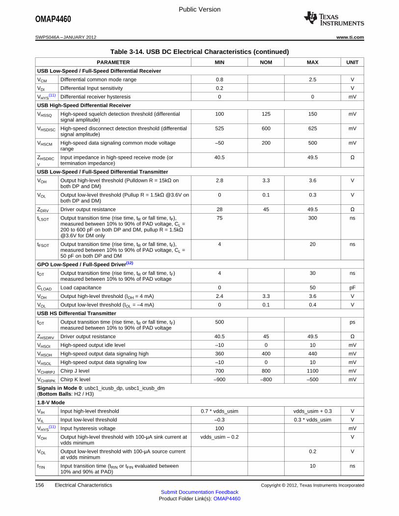
Public Version
OMAP4460
SWPS046A –JANUARY 2012 www.ti.com
Table 3-14. USB DC Electrical Characteristics (continued)
PARAMETER MIN NOM MAX UNIT
USB Low-Speed / Full-Speed Differential Receiver
VCM Differential common mode range 0.8 2.5 V
VDI Differential Input sensitivity 0.2 V
VHYS(11) Differential receiver hysteresis 0 0 mV
USB High-Speed Differential Receiver
VHSSQ High-speed squelch detection threshold (differential 100 125 150 mVsignal amplitude)
VHSDISC High-speed disconnect detection threshold (differential 525 600 625 mVsignal amplitude)
VHSCM High-speed data signaling common mode voltage –50 200 500 mVrange
ZHSDRC Input impedance in high-speed receive mode (or 40.5 49.5 ΩV termination impedance)
USB Low-Speed / Full-Speed Differential Transmitter
VOH Output high-level threshold (Pulldown R = 15kΩ on 2.8 3.3 3.6 Vboth DP and DM)
VOL Output low-level threshold (Pullup R = 1.5kΩ @3.6V on 0 0.1 0.3 Vboth DP and DM)
ZDRV Driver output resistance 28 45 49.5 ΩtLSOT Output transition time (rise time, tR or fall time, tF), 75 300 ns
measured between 10% to 90% of PAD voltage, CL =200 to 600 pF on both DP and DM, pullup R = 1.5kΩ@3.6V for DM only
tFSOT Output transition time (rise time, tR or fall time, tF), 4 20 nsmeasured between 10% to 90% of PAD voltage, CL =50 pF on both DP and DM
GPO Low-Speed / Full-Speed Driver(12)
tOT Output transition time (rise time, tR or fall time, tF) 4 30 nsmeasured between 10% to 90% of PAD voltage
CLOAD Load capacitance 0 50 pF
VOH Output high-level threshold (IOH = 4 mA) 2.4 3.3 3.6 V
VOL Output low-level threshold (IOL = –4 mA) 0 0.1 0.4 V
USB HS Differential Transmitter
tOT Output transition time (rise time, tR or fall time, tF) 500 psmeasured between 10% to 90% of PAD voltage
ZHSDRV Driver output resistance 40.5 45 49.5 ΩVHSOI High-speed output idle level –10 0 10 mV
VHSOH High-speed output data signaling high 360 400 440 mV
VHSOL High-speed output data signaling low –10 0 10 mV
VCHIRPJ Chirp J level 700 800 1100 mV
VCHIRPK Chirp K level –900 –800 –500 mV
Signals in Mode 0: usbc1_icusb_dp, usbc1_icusb_dm(Bottom Balls: H2 / H3)
1.8-V Mode
VIH Input high-level threshold 0.7 * vdds_usim vdds_usim + 0.3 V
VIL Input low-level threshold –0.3 0.3 * vdds_usim V
VHYS(11) Input hysteresis voltage 100 mV
VOH Output high-level threshold with 100-µA sink current at vdds_usim – 0.2 Vvdds minimum
VOL Output low-level threshold with 100-µA source current 0.2 Vat vdds minimum
tTIN Input transition time (tRIN or tFIN evaluated between 10 ns10% and 90% at PAD)
156 Electrical Characteristics Copyright © 2012, Texas Instruments Incorporated
Submit Documentation FeedbackProduct Folder Link(s): OMAP4460

Public Version
OMAP4460
www.ti.com SWPS046A –JANUARY 2012
Table 3-14. USB DC Electrical Characteristics (continued)
PARAMETER MIN NOM MAX UNIT
tOT Output transition time at 30-pf High-Speed 3 nsload (rise time, tROUT or fall SPEEDCTRL = 1time, tFOUT), measuredbetween 10% to 90% of PADvoltage
Output transition time at 30-pf Normal 8 nsload (rise time, tROUT or fall SPEEDCTRL = 0time, tFOUT), measuredbetween 30% to 70% of PADvoltage
CLOAD Load capacitance 10 30 pF
3.0-V Mode
VIH Input high-level threshold 0.625 * vdds_usim vdds_usim + 0.3 V
VIL Input low-level threshold –0.3 0.25 * vdds_usim V
VHYS(11) Input hysteresis threshold 50 mV
VOH Output high-level threshold with 100-µA sink current at 0.75 * vdds_usim Vvdds minimum
VOL Output low-level threshold with 100-µA source current 0.125 * vdds_usim Vat vdds minimum
tTIN Input transition time (tRIN or tFIN evaluated between 10 ns10% and 90% at PAD)
tOT Output transition time at 30-pf High-Speed 3 nsload (rise time, tROUT or fall SPEEDCTRL = 1time, tFOUT), measuredbetween 10% to 90% of PADvoltage
Output transition time at 30-pf Normal 8 nsload (rise time, tROUT or fall SPEEDCTRL = 0time, tFOUT), measuredbetween 30% to 70% of PADvoltage
CLOAD Load capacitance 10 30 pF
(1) Output transition time measured between 20% to 70% of PAD voltage
(2) Output transition time measured between 20% to 80% of PAD voltage
(3) Output transition time measured between 10% to 90% of PAD voltage
(4) In vdds_dv_y, y can have the value: bank0 or bank6 depending on the ball used. For more information on a ball and the correspondingpower, see Table 2-1, POWER [9] column.
(5) Buffer is designed for high-speed application where input slew rates are more than 1 V/ns. It is fast enough to not have any noise on thesignal during transition and hysteresis is not required.
(6) RREF (reference output impedance) is considered to be the production trim setting for Drv8 mode, with RREF = 50 Ω, which correspondsto ZO = 50 Ω (IOUT = 8 mA). For a full description of the output impedance setting, see the the Control Module / Control ModuleFunctional Description / Functional Register Description / Signal Integrity Parameter Control Registers With Pad Group Assignmentsection of the OMAP4460 TRM.
(7) To achieve optimal noise/speed trade off, the slew rate (turn-on time) of the output signal can be programmed using the slew ratecontrol bits sr[1:0]. Please note that the control bits sr[1:0] do not affect the driver DC drive-strength. They only control the driver turn-ontime. It is to be noted that turn-on time and maximum supply noise are the parameter defined to help user make relative comparison andcorrelate the driver operation at different turn-on time settings.
(8) Output transition time/turn-on time for Drv8 setting, i[2:0] = 011. For a full description of this setting, see the Control Module / ControlModule Functional Description / Functional Register Description / Signal Integrity Parameter Control Registers With Pad GroupAssignment section of the OMAP4460 TRM.
(9) Maximum noise (peak-peak) on the IO supply voltage for Drv8 setting, i[2:0] = 011.
(10) The measurement setup (see Figure 3-1 and Figure 3-2) is not intended as a precise representation of any particular systemenvironment or a depiction of the actual load presented. Maximum output supply noise, (see Figure 3-2, L*di/dt) on the IO supply ismeasured with 1 nH of inductance on the IO supply.
(11) VHYS is the magnitude of the difference between the positive-going threshold voltage VT+ and the negative-going threshold voltage VT–.
(12) The GPIO modes are only available through multiplexing mode 1 or 2. For more information, see Table 2-1.
Copyright © 2012, Texas Instruments Incorporated Electrical Characteristics 157Submit Documentation Feedback
Product Folder Link(s): OMAP4460
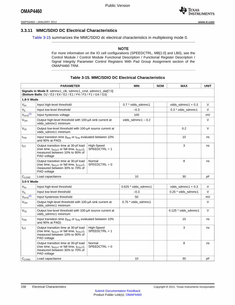
Public Version
OMAP4460
SWPS046A –JANUARY 2012 www.ti.com
3.3.11 MMC/SDIO DC Electrical Characteristics
Table 3-15 summarizes the MMC/SDIO dc electrical characteristics in multiplexing mode 0.
NOTEFor more information on the IO cell configurations (SPEEDCTRL, MB[1:0] and LB0), see theControl Module / Control Module Functional Description / Functional Register Description /Signal Integrity Parameter Control Registers With Pad Group Assignment section of theOMAP4460 TRM.
Table 3-15. MMC/SDIO DC Electrical Characteristics
PARAMETER MIN NOM MAX UNIT
Signals in Mode 0: sdmmc1_clk, sdmmc1_cmd, sdmmc1_dat[7:0](Bottom Balls: D2 / E3 / E4 / E2 / E1 / F4 / F3 / F1 / G4 / G3)
1.8-V Mode
VIH Input high-level threshold 0.7 * vdds_sdmmc1 vdds_sdmmc1 + 0.3 V
VIL Input low-level threshold –0.3 0.3 * vdds_sdmmc1 V
VHYS(2) Input hysteresis voltage 100 mV
VOH Output high-level threshold with 100-µA sink current at vdds_sdmmc1 – 0.2 Vvdds_sdmmc1 minimum
VOL Output low-level threshold with 100-µA source current at 0.2 Vvdds_sdmmc1 minimum
tTIN Input transition time (tRIN or tFIN evaluated between 10% 10 nsand 90% at PAD)
tOT Output transition time at 30-pf load High-Speed 3 ns(rise time, tROUT or fall time, tFOUT), SPEEDCTRL = 1measured between 10% to 90% ofPAD voltage
Output transition time at 30-pf load Normal 8 ns(rise time, tROUT or fall time, tFOUT), SPEEDCTRL = 0measured between 30% to 70% ofPAD voltage
CLOAD Load capacitance 10 30 pF
3.0-V Mode
VIH Input high-level threshold 0.625 * vdds_sdmmc1 vdds_sdmmc1 + 0.3 V
VIL Input low-level threshold –0.3 0.25 * vdds_sdmmc1 V
VHYS(2) Input hysteresis threshold 50 mV
VOH Output high-level threshold with 100-µA sink current at 0.75 * vdds_sdmmc1 Vvdds_sdmmc1 minimum
VOL Output low-level threshold with 100-µA source current at 0.125 * vdds_sdmmc1 Vvdds_sdmmc1 minimum
tTIN Input transition time (tRIN or tFIN evaluated between 10% 10 nsand 90% at PAD)
tOT Output transition time at 30-pf load High-Speed 3 ns(rise time, tROUT or fall time, tFOUT), SPEEDCTRL = 1measured between 10% to 90% ofPAD voltage
Output transition time at 30-pf load Normal 8 ns(rise time, tROUT or fall time, tFOUT), SPEEDCTRL = 0measured between 30% to 70% ofPAD voltage
CLOAD Load capacitance 10 30 pF
158 Electrical Characteristics Copyright © 2012, Texas Instruments Incorporated
Submit Documentation FeedbackProduct Folder Link(s): OMAP4460
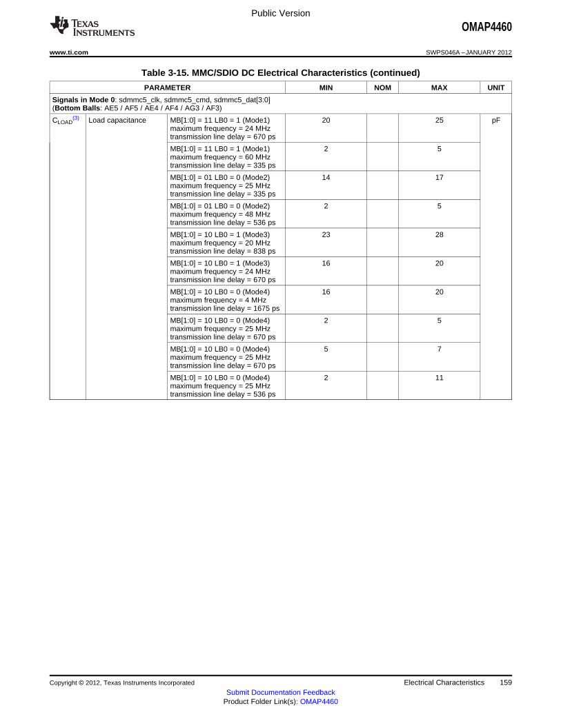
Public Version
OMAP4460
www.ti.com SWPS046A –JANUARY 2012
Table 3-15. MMC/SDIO DC Electrical Characteristics (continued)
PARAMETER MIN NOM MAX UNIT
Signals in Mode 0: sdmmc5_clk, sdmmc5_cmd, sdmmc5_dat[3:0](Bottom Balls: AE5 / AF5 / AE4 / AF4 / AG3 / AF3)
CLOAD(3) Load capacitance MB[1:0] = 11 LB0 = 1 (Mode1) 20 25 pF
maximum frequency = 24 MHztransmission line delay = 670 ps
MB[1:0] = 11 LB0 = 1 (Mode1) 2 5maximum frequency = 60 MHztransmission line delay = 335 ps
MB[1:0] = 01 LB0 = 0 (Mode2) 14 17maximum frequency = 25 MHztransmission line delay = 335 ps
MB[1:0] = 01 LB0 = 0 (Mode2) 2 5maximum frequency = 48 MHztransmission line delay = 536 ps
MB[1:0] = 10 LB0 = 1 (Mode3) 23 28maximum frequency = 20 MHztransmission line delay = 838 ps
MB[1:0] = 10 LB0 = 1 (Mode3) 16 20maximum frequency = 24 MHztransmission line delay = 670 ps
MB[1:0] = 10 LB0 = 0 (Mode4) 16 20maximum frequency = 4 MHztransmission line delay = 1675 ps
MB[1:0] = 10 LB0 = 0 (Mode4) 2 5maximum frequency = 25 MHztransmission line delay = 670 ps
MB[1:0] = 10 LB0 = 0 (Mode4) 5 7maximum frequency = 25 MHztransmission line delay = 670 ps
MB[1:0] = 10 LB0 = 0 (Mode4) 2 11maximum frequency = 25 MHztransmission line delay = 536 ps
Copyright © 2012, Texas Instruments Incorporated Electrical Characteristics 159Submit Documentation Feedback
Product Folder Link(s): OMAP4460

Public Version
OMAP4460
SWPS046A –JANUARY 2012 www.ti.com
Table 3-15. MMC/SDIO DC Electrical Characteristics (continued)
PARAMETER MIN NOM MAX UNIT
tOT(3) Output transition time MB[1:0] = 11 LB0 = 1 (Mode1) 10 ns
(rise time, tR or fall maximum frequency = 24 MHztime, tF) measured transmission line delay = 670 psbetween 10% to 90% MB[1:0] = 11 LB0 = 1 (Mode1) 4of PAD voltage, the maximum frequency = 60 MHzmaximum at the transmission line delay = 335 psmaximum load
MB[1:0] = 01 LB0 = 0 (Mode2) 5.6(1)
maximum frequency = 25 MHztransmission line delay = 335 ps
MB[1:0] = 01 LB0 = 0 (Mode2) 6.3maximum frequency = 48 MHztransmission line delay = 536 ps
MB[1:0] = 10 LB0 = 1 (Mode3) 10.5(1)
maximum frequency = 20 MHztransmission line delay = 838 ps
MB[1:0] = 10 LB0 = 1 (Mode3) 12.5maximum frequency = 24 MHztransmission line delay = 670 ps
MB[1:0] = 10 LB0 = 0 (Mode4) 16.8(1)
maximum frequency = 4 MHztransmission line delay = 1675 ps
MB[1:0] = 10 LB0 = 0 (Mode4) 10maximum frequency = 25 MHztransmission line delay = 670 ps
MB[1:0] = 10 LB0 = 0 (Mode4) 12.2maximum frequency = 25 MHztransmission line delay = 670 ps
MB[1:0] = 10 LB0 = 0 (Mode4) 8(1)
maximum frequency = 25 MHztransmission line delay = 536 ps
1.2-V Mode
VIH Input high-level threshold 0.65 * vdds_dv_bank4 vdds_dv_bank4 + 0.3 V
VIL Input low-level threshold –0.3 0.35 * vdds_dv_bank4 V
VHYS(2) Input hysteresis voltage 135 mV
VOH Output high-level threshold (IOH = 4 mA) 0.75 * vdds_dv_bank4 V
VOL Output low-level threshold (IOL = 4 mA) 0.25 * vdds_dv_bank4 V
1.8-V Mode
VIH Input high-level threshold 0.65 * vdds_dv_bank4 vdds_dv_bank4 + 0.3 V
VIL Input low-level threshold –0.3 0.35 * vdds_dv_bank4 V
VHYS(2) Input hysteresis voltage 150 mV
VOH Output high-level threshold (IOH = 4 mA) vdds_dv_bank4 – 0.45 V
VOL Output low-level threshold (IOL = 4 mA) 0.45 V
(1) Output transition time measured between 20% to 80% of PAD voltage.
(2) VHYS is the magnitude of the difference between the positive-going threshold voltage VT+ and the negative-going threshold voltage VT–.
(3) Depending on the programming mode, different output load and transition time are available following the targeted maximum frequency,transmission line or output transition time.
160 Electrical Characteristics Copyright © 2012, Texas Instruments Incorporated
Submit Documentation FeedbackProduct Folder Link(s): OMAP4460

Public Version
OMAP4460
www.ti.com SWPS046A –JANUARY 2012
3.3.12 USIM DC Electrical Characteristics
Table 3-16 summarizes the USIM dc electrical characteristics in multiplexing mode 0.
NOTEFor more information on the IO cell configurations (SC[1:0]), see the Control Module /Control Module Functional Description / Functional Register Description / Signal IntegrityParameter Control Registers With Pad Group Assignment section of the OMAP4460 TRM.
Table 3-16. USIM DC Electrical Characteristics
PARAMETER MIN NOM MAX UNIT
Signals in Mode 0: sim_io, sim_clk, sim_reset(Bottom Balls: H4 / J2 / G2)
1.8-V Mode
VIH Input high-level threshold 0.7 * vdds_usim vdds_usim + 0.3 V
VIL Input low-level threshold –0.3 0.2 * vdds_usim V
VHYS(1) Input hysteresis voltage 100 mV
CIN Input capacitance 2.5 pF
VOH Output high-level threshold with 20-µA sink current 0.8 * vdds_usim vdds_usim + 0.3 V
VOL Output low-level threshold with 1-mA source current at –0.3 0.4 Vvdds
tTIN Input transition time (tRIN or tFIN evaluated between 10 ns10% and 90% at PAD)
tOT Output transition time at 30-pF load (rise time, tROUT or 35 nsfall time, tFOUT), measured between 10% to 90% ofPAD voltage
CLOAD Load capacitance 10 30 pF
3.0-V Mode
VIH Input high-level threshold 0.7 * vdds_usim vdds_usim + 0.3 V
VIL Input low-level threshold –0.3 0.2 * vdds_usim V
VHYS(1) Input hysteresis voltage 50 mV
CIN Input capacitance 2.5 pF
VOH Output high-level threshold with 20-µA sink current 0.7 * vdds_usim vdds_usim + 0.3 V
VOL Output low-level threshold with 1-mA source current at –0.3 0.4 Vvdds
tTIN Input transition time (tRIN or tFIN evaluated between 10 ns10% and 90% at PAD)
tOT Output transition time at 30-pF load (rise time, tROUT or 35 nsfall time, tFOUT), measured between 10% to 90% ofPAD voltage
CLOAD Load capacitance 10 30 pF
Signal in Mode 0: sim_cd(Bottom Ball: J1)
1.8-V Mode
VIH Input high-level threshold 0.65 * vdds_1p8v vdds_1p8v + 0.3 V
VIL Input low-level threshold –0.3 0.35 * vdds_1p8v V
VHYS(1) Input hysteresis voltage 150 mV
VOH Output high-level threshold (IOH = –4 mA) vdds_1p8v – 0.45 V
VOL Output low-level threshold (IOL = 4 mA) 0.45 V
Signal in Mode 0: sim_pwrctrl(Bottom Ball: K1)
Copyright © 2012, Texas Instruments Incorporated Electrical Characteristics 161Submit Documentation Feedback
Product Folder Link(s): OMAP4460

Public Version
OMAP4460
SWPS046A –JANUARY 2012 www.ti.com
Table 3-16. USIM DC Electrical Characteristics (continued)
PARAMETER MIN NOM MAX UNIT
CLOAD Load capacitance SC[1:0] = 00 4 60 pF
SC[1:0] = 01 2 21
SC[1:0] = 10 7 33
tOT Output transition time (rise time, tR SC[1:0] = 00 1 15 nsor fall time, tF) measured between SC[1:0] = 01 0.4 510% to 90% of PAD voltage,
SC[1:0] = 10 0.6 7minimum at the minimum load andmaximum at the maximum load
1.8-V Mode
VIH Input high-level threshold 0.65 * vdds_1p8v vdds_1p8v + 0.3 V
VIL Input low-level threshold –0.3 0.35 * vdds_1p8v V
VHYS(1) Input hysteresis voltage 150 mV
VOH Output high-level threshold (IOH = –4 mA) vdds_1p8v – 0.45 V
VOL Output low-level threshold (IOL = 4 mA) 0.45 V
(1) VHYS is the magnitude of the difference between the positive-going threshold voltage VT+ and the negative-going threshold voltage VT–.
162 Electrical Characteristics Copyright © 2012, Texas Instruments Incorporated
Submit Documentation FeedbackProduct Folder Link(s): OMAP4460
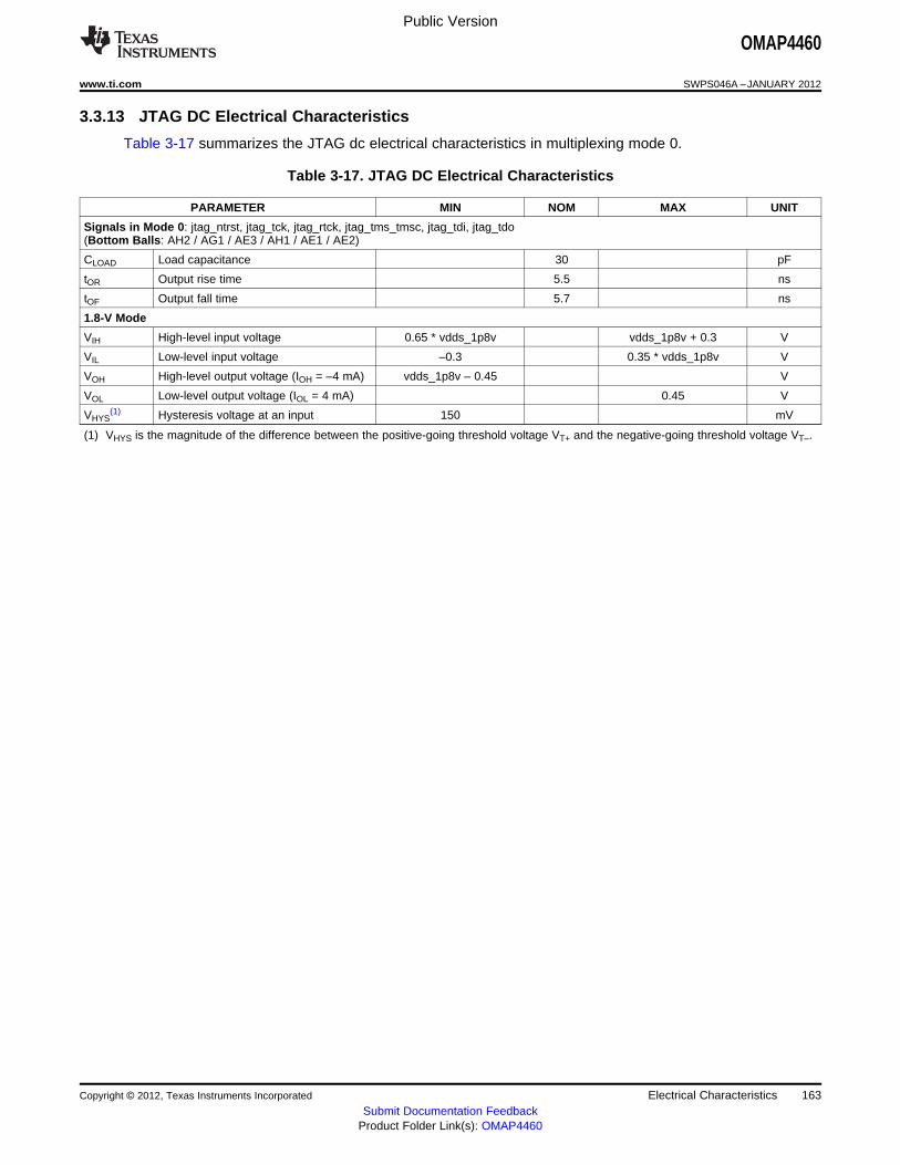
Public Version
OMAP4460
www.ti.com SWPS046A –JANUARY 2012
3.3.13 JTAG DC Electrical Characteristics
Table 3-17 summarizes the JTAG dc electrical characteristics in multiplexing mode 0.
Table 3-17. JTAG DC Electrical Characteristics
PARAMETER MIN NOM MAX UNIT
Signals in Mode 0: jtag_ntrst, jtag_tck, jtag_rtck, jtag_tms_tmsc, jtag_tdi, jtag_tdo(Bottom Balls: AH2 / AG1 / AE3 / AH1 / AE1 / AE2)
CLOAD Load capacitance 30 pF
tOR Output rise time 5.5 ns
tOF Output fall time 5.7 ns
1.8-V Mode
VIH High-level input voltage 0.65 * vdds_1p8v vdds_1p8v + 0.3 V
VIL Low-level input voltage –0.3 0.35 * vdds_1p8v V
VOH High-level output voltage (IOH = –4 mA) vdds_1p8v – 0.45 V
VOL Low-level output voltage (IOL = 4 mA) 0.45 V
VHYS(1) Hysteresis voltage at an input 150 mV
(1) VHYS is the magnitude of the difference between the positive-going threshold voltage VT+ and the negative-going threshold voltage VT–.
Copyright © 2012, Texas Instruments Incorporated Electrical Characteristics 163Submit Documentation Feedback
Product Folder Link(s): OMAP4460
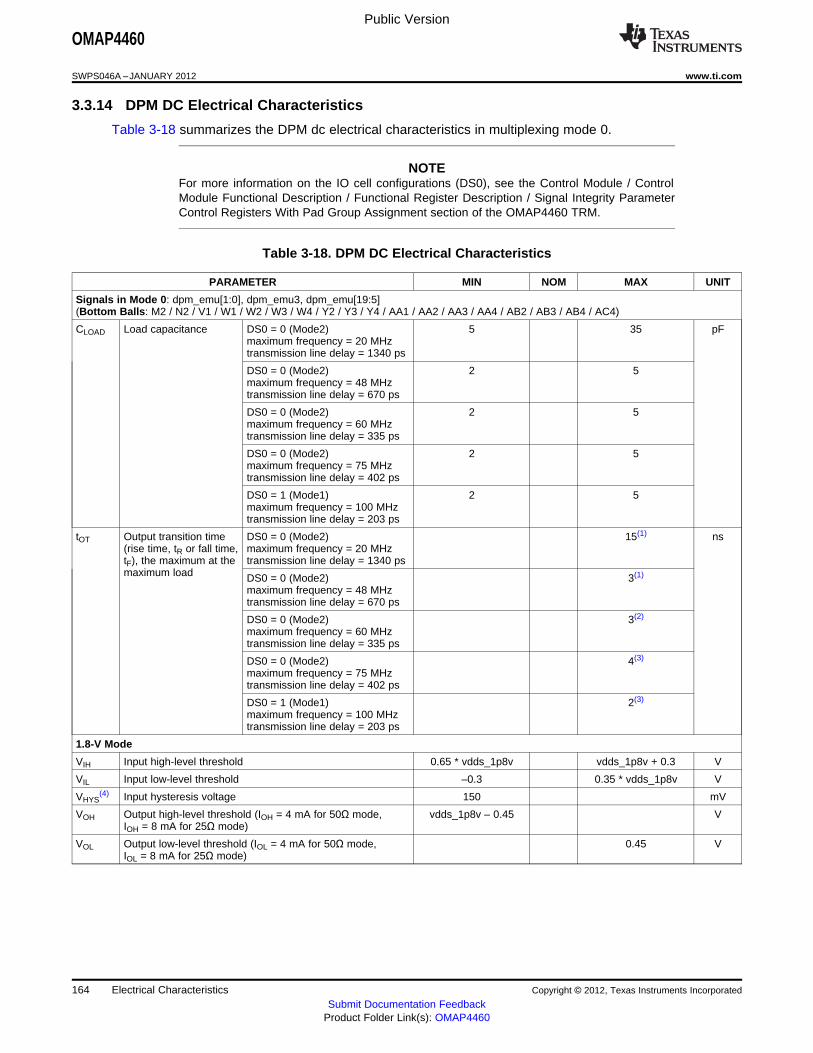
Public Version
OMAP4460
SWPS046A –JANUARY 2012 www.ti.com
3.3.14 DPM DC Electrical Characteristics
Table 3-18 summarizes the DPM dc electrical characteristics in multiplexing mode 0.
NOTEFor more information on the IO cell configurations (DS0), see the Control Module / ControlModule Functional Description / Functional Register Description / Signal Integrity ParameterControl Registers With Pad Group Assignment section of the OMAP4460 TRM.
Table 3-18. DPM DC Electrical Characteristics
PARAMETER MIN NOM MAX UNIT
Signals in Mode 0: dpm_emu[1:0], dpm_emu3, dpm_emu[19:5](Bottom Balls: M2 / N2 / V1 / W1 / W2 / W3 / W4 / Y2 / Y3 / Y4 / AA1 / AA2 / AA3 / AA4 / AB2 / AB3 / AB4 / AC4)
CLOAD Load capacitance DS0 = 0 (Mode2) 5 35 pFmaximum frequency = 20 MHztransmission line delay = 1340 ps
DS0 = 0 (Mode2) 2 5maximum frequency = 48 MHztransmission line delay = 670 ps
DS0 = 0 (Mode2) 2 5maximum frequency = 60 MHztransmission line delay = 335 ps
DS0 = 0 (Mode2) 2 5maximum frequency = 75 MHztransmission line delay = 402 ps
DS0 = 1 (Mode1) 2 5maximum frequency = 100 MHztransmission line delay = 203 ps
tOT Output transition time DS0 = 0 (Mode2) 15(1) ns(rise time, tR or fall time, maximum frequency = 20 MHztF), the maximum at the transmission line delay = 1340 psmaximum load DS0 = 0 (Mode2) 3(1)
maximum frequency = 48 MHztransmission line delay = 670 ps
DS0 = 0 (Mode2) 3(2)
maximum frequency = 60 MHztransmission line delay = 335 ps
DS0 = 0 (Mode2) 4(3)
maximum frequency = 75 MHztransmission line delay = 402 ps
DS0 = 1 (Mode1) 2(3)
maximum frequency = 100 MHztransmission line delay = 203 ps
1.8-V Mode
VIH Input high-level threshold 0.65 * vdds_1p8v vdds_1p8v + 0.3 V
VIL Input low-level threshold –0.3 0.35 * vdds_1p8v V
VHYS(4) Input hysteresis voltage 150 mV
VOH Output high-level threshold (IOH = 4 mA for 50Ω mode, vdds_1p8v – 0.45 VIOH = 8 mA for 25Ω mode)
VOL Output low-level threshold (IOL = 4 mA for 50Ω mode, 0.45 VIOL = 8 mA for 25Ω mode)
164 Electrical Characteristics Copyright © 2012, Texas Instruments Incorporated
Submit Documentation FeedbackProduct Folder Link(s): OMAP4460

Public Version
OMAP4460
www.ti.com SWPS046A –JANUARY 2012
Table 3-18. DPM DC Electrical Characteristics (continued)
PARAMETER MIN NOM MAX UNIT
Signals in Mode 0: dpm_emu2, dpm_emu4(Bottom Balls: P2 / V2)
CLOAD Load capacitance DS0 = 0 (Mode2) 5 35 pFmaximum frequency = 20 MHztransmission line delay = 1340 ps
DS0 = 0 (Mode2) 2 5maximum frequency = 48 MHztransmission line delay = 670 ps
DS0 = 0 (Mode2) 2 5maximum frequency = 60 MHztransmission line delay = 335 ps
DS0 = 0 (Mode2) 2 5maximum frequency = 75 MHztransmission line delay = 402 ps
DS0 = 1 (Mode1) 2 5maximum frequency = 100 MHztransmission line delay = 203 ps
tOT Output transition time DS0 = 0 (Mode2) 15(1) ns(rise time, tR or fall time, maximum frequency = 20 MHztF), the maximum at the transmission line delay = 1340 psmaximum load DS0 = 0 (Mode2) 3(1)
maximum frequency = 48 MHztransmission line delay = 670 ps
DS0 = 0 (Mode2) 3(2)
maximum frequency = 60 MHztransmission line delay = 335 ps
DS0 = 0 (Mode2) 4(3)
maximum frequency = 75 MHztransmission line delay = 402 ps
DS0 = 1 (Mode1) 2(3)
maximum frequency = 100 MHztransmission line delay = 203 ps
1.8-V Mode
VIH Input high-level threshold 0.65 * vdds_1p8v vdds_1p8v + 0.3 V
VIL Input low-level threshold –0.3 0.35 * vdds_1p8v V
VHYS(4) Input hysteresis voltage 70 mV
VOH Output high-level threshold (IOH = 4 mA for 50Ω mode, vdds_1p8v – 0.45 VIOH = 8 mA for 25Ω mode)
VOL Output low-level threshold (IOL = 4 mA for 50Ω mode, 0.45 VIOL = 8 mA for 25Ω mode)
(1) Output transition time measured between 20% to 70% of PAD voltage.
(2) Output transition time measured between 20% to 80% of PAD voltage.
(3) Output transition time measured between 10% to 90% of PAD voltage.
(4) VHYS is the magnitude of the difference between the positive-going threshold voltage VT+ and the negative-going threshold voltage VT–.
Copyright © 2012, Texas Instruments Incorporated Electrical Characteristics 165Submit Documentation Feedback
Product Folder Link(s): OMAP4460
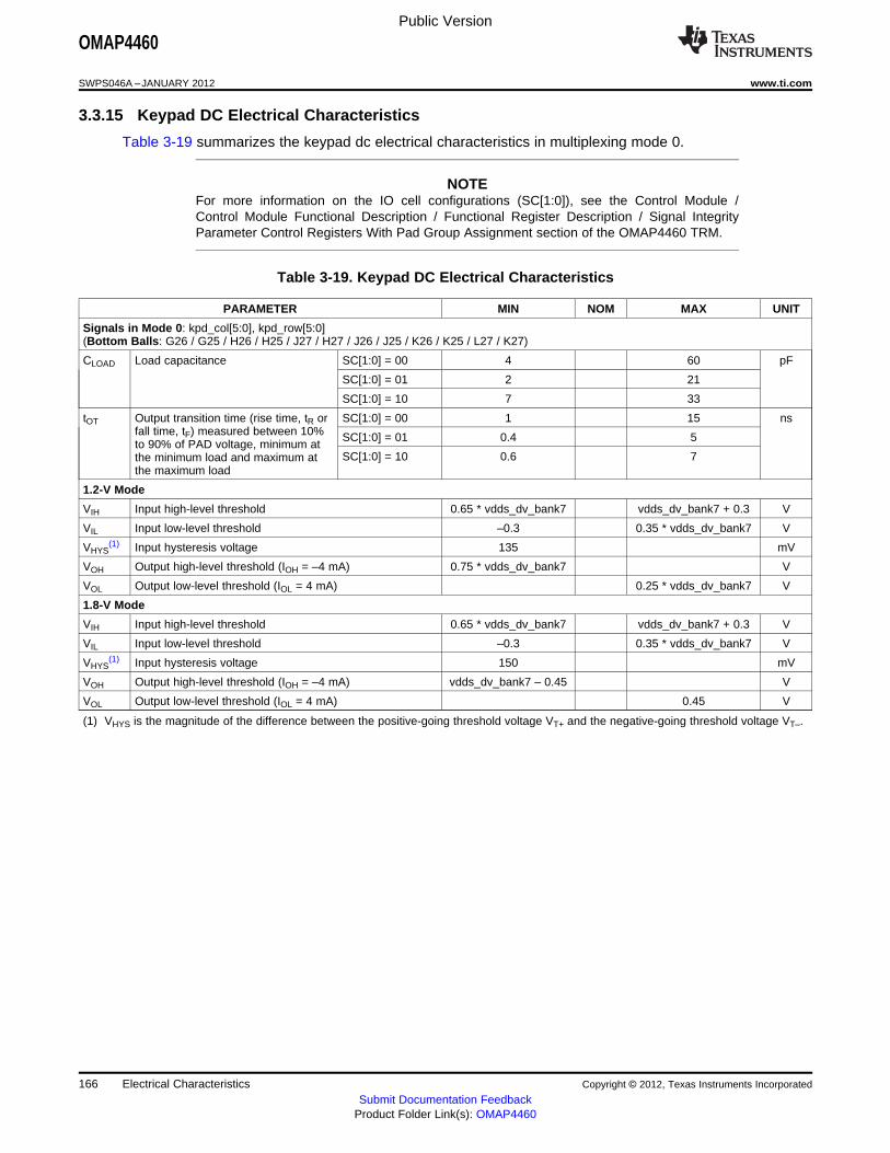
Public Version
OMAP4460
SWPS046A –JANUARY 2012 www.ti.com
3.3.15 Keypad DC Electrical Characteristics
Table 3-19 summarizes the keypad dc electrical characteristics in multiplexing mode 0.
NOTEFor more information on the IO cell configurations (SC[1:0]), see the Control Module /Control Module Functional Description / Functional Register Description / Signal IntegrityParameter Control Registers With Pad Group Assignment section of the OMAP4460 TRM.
Table 3-19. Keypad DC Electrical Characteristics
PARAMETER MIN NOM MAX UNIT
Signals in Mode 0: kpd_col[5:0], kpd_row[5:0](Bottom Balls: G26 / G25 / H26 / H25 / J27 / H27 / J26 / J25 / K26 / K25 / L27 / K27)
CLOAD Load capacitance SC[1:0] = 00 4 60 pF
SC[1:0] = 01 2 21
SC[1:0] = 10 7 33
tOT Output transition time (rise time, tR or SC[1:0] = 00 1 15 nsfall time, tF) measured between 10% SC[1:0] = 01 0.4 5to 90% of PAD voltage, minimum at
SC[1:0] = 10 0.6 7the minimum load and maximum atthe maximum load
1.2-V Mode
VIH Input high-level threshold 0.65 * vdds_dv_bank7 vdds_dv_bank7 + 0.3 V
VIL Input low-level threshold –0.3 0.35 * vdds_dv_bank7 V
VHYS(1) Input hysteresis voltage 135 mV
VOH Output high-level threshold (IOH = –4 mA) 0.75 * vdds_dv_bank7 V
VOL Output low-level threshold (IOL = 4 mA) 0.25 * vdds_dv_bank7 V
1.8-V Mode
VIH Input high-level threshold 0.65 * vdds_dv_bank7 vdds_dv_bank7 + 0.3 V
VIL Input low-level threshold –0.3 0.35 * vdds_dv_bank7 V
VHYS(1) Input hysteresis voltage 150 mV
VOH Output high-level threshold (IOH = –4 mA) vdds_dv_bank7 – 0.45 V
VOL Output low-level threshold (IOL = 4 mA) 0.45 V
(1) VHYS is the magnitude of the difference between the positive-going threshold voltage VT+ and the negative-going threshold voltage VT–.
166 Electrical Characteristics Copyright © 2012, Texas Instruments Incorporated
Submit Documentation FeedbackProduct Folder Link(s): OMAP4460

Public Version
OMAP4460
www.ti.com SWPS046A –JANUARY 2012
3.3.16 System DC Electrical Characteristics
Table 3-20 summarizes the system dc electrical characteristics in multiplexing mode 0.
NOTEFor more information on the IO cell configurations (SC[1:0], MB[1:0] and LB0), see theControl Module / Control Module Functional Description / Functional Register Description /Signal Integrity Parameter Control Registers With Pad Group Assignment section of theOMAP4460 TRM.
Table 3-20. System DC Electrical Characteristics
PARAMETER MIN NOM MAX UNIT
Signals in Mode 0: sys_nrespwron, sys_nreswarm(Bottom Balls: AE7, AF7)
1.8-V Mode
VIH Input high-level threshold 0.65 * vdds_1p8v vdds_1p8v + 0.3 V
VIL Input low-level threshold –0.3 0.35 * vdds_1p8v V
VHYS(4) Input hysteresis voltage 150 mV
VOH Output high-level threshold (IOH = –4 mA) vdds_1p8v – 0.45 V
VOL Output low-level threshold (IOL = 4 mA) 0.45 V
Signals in Mode 0: fref_clk_ioreq, sys_32k, sys_pwr_req, sys_pwron_reset_out, sys_boot[7:6](Bottom Balls: AD1 / AG7 / AH7 / AG6 / AF8 / AE8)
CLOAD Load capacitance SC[1:0] = 00 4 60 pF
SC[1:0] = 01 2 21
SC[1:0] = 10 7 33
tOT Output transition time (rise time, tR or SC[1:0] = 00 1 15 nsfall time, tF) measured between 10% SC[1:0] = 01 0.4 5to 90% of PAD voltage, minimum at
SC[1:0] = 10 0.6 7the minimum load and maximum atthe maximum load
1.8-V Mode
VIH Input high-level threshold 0.65 * vdds_y(1) vdds_y(1) + 0.3 V
VIL Input low-level threshold –0.3 0.35 * vdds_y(1) V
VHYS(4) Input hysteresis voltage 150 mV
VOH Output high-level threshold (IOH = –4 mA) vdds_y(1) – 0.45 V
VOL Output low-level threshold (IOL = 4 mA) 0.45 V
Signals in Mode 0: sys_nirq[2:1], sys_boot[5:0](Bottom Balls: AE6 / AF6 / F26 / E27 / E26 / E25 / D28 / D27)
CLOAD Load capacitance SC[1:0] = 00 4 60 pF
SC[1:0] = 01 2 21
SC[1:0] = 10 7 33
tOT Output transition time (rise time, tR or SC[1:0] = 00 1 15 nsfall time, tF) measured between 10% SC[1:0] = 01 0.4 5to 90% of PAD voltage, minimum at
SC[1:0] = 10 0.6 7the minimum load and maximum atthe maximum load
1.8-V Mode
VIH Input high-level threshold 0.65 * vdds_1p8v vdds_1p8v + 0.3 V
VIL Input low-level threshold –0.3 0.35 * vdds_1p8v V
VHYS(4) Input hysteresis voltage 150 mV
VOH Output high-level threshold (IOH = –4 mA) vdds_1p8v – 0.45 V
VOL Output low-level threshold (IOL = 4 mA) 0.45 V
Copyright © 2012, Texas Instruments Incorporated Electrical Characteristics 167Submit Documentation Feedback
Product Folder Link(s): OMAP4460
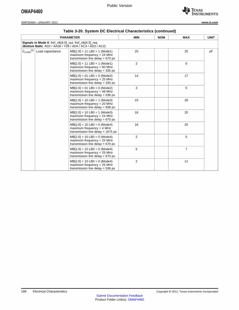
Public Version
OMAP4460
SWPS046A –JANUARY 2012 www.ti.com
Table 3-20. System DC Electrical Characteristics (continued)
PARAMETER MIN NOM MAX UNIT
Signals in Mode 0: fref_clk[4:0]_out, fref_clk[4:3]_req(Bottom Balls: AD2 / AA28 / Y28 / AD4 / AC3 / AD3 / AC2)
CLOAD(5) Load capacitance MB[1:0] = 11 LB0 = 1 (Mode1) 20 25 pF
maximum frequency = 24 MHztransmission line delay = 670 ps
MB[1:0] = 11 LB0 = 1 (Mode1) 2 5maximum frequency = 60 MHztransmission line delay = 335 ps
MB[1:0] = 01 LB0 = 0 (Mode2) 14 17maximum frequency = 25 MHztransmission line delay = 335 ps
MB[1:0] = 01 LB0 = 0 (Mode2) 2 5maximum frequency = 48 MHztransmission line delay = 536 ps
MB[1:0] = 10 LB0 = 1 (Mode3) 23 28maximum frequency = 20 MHztransmission line delay = 838 ps
MB[1:0] = 10 LB0 = 1 (Mode3) 16 20maximum frequency = 24 MHztransmission line delay = 670 ps
MB[1:0] = 10 LB0 = 0 (Mode4) 16 20maximum frequency = 4 MHztransmission line delay = 1675 ps
MB[1:0] = 10 LB0 = 0 (Mode4) 2 5maximum frequency = 25 MHztransmission line delay = 670 ps
MB[1:0] = 10 LB0 = 0 (Mode4) 5 7maximum frequency = 25 MHztransmission line delay = 670 ps
MB[1:0] = 10 LB0 = 0 (Mode4) 2 11maximum frequency = 25 MHztransmission line delay = 536 ps
168 Electrical Characteristics Copyright © 2012, Texas Instruments Incorporated
Submit Documentation FeedbackProduct Folder Link(s): OMAP4460
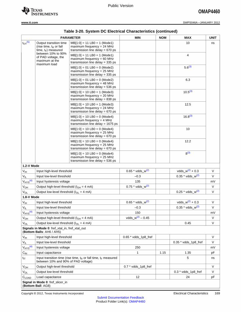
Public Version
OMAP4460
www.ti.com SWPS046A –JANUARY 2012
Table 3-20. System DC Electrical Characteristics (continued)
PARAMETER MIN NOM MAX UNIT
tOT(5) Output transition time MB[1:0] = 11 LB0 = 1 (Mode1) 10 ns
(rise time, tR or fall maximum frequency = 24 MHztime, tF) measured transmission line delay = 670 psbetween 10% to 90% MB[1:0] = 11 LB0 = 1 (Mode1) 4of PAD voltage, the maximum frequency = 60 MHzmaximum at the transmission line delay = 335 psmaximum load
MB[1:0] = 01 LB0 = 0 (Mode2) 5.6(3)
maximum frequency = 25 MHztransmission line delay = 335 ps
MB[1:0] = 01 LB0 = 0 (Mode2) 6.3maximum frequency = 48 MHztransmission line delay = 536 ps
MB[1:0] = 10 LB0 = 1 (Mode3) 10.5(3)
maximum frequency = 20 MHztransmission line delay = 838 ps
MB[1:0] = 10 LB0 = 1 (Mode3) 12.5maximum frequency = 24 MHztransmission line delay = 670 ps
MB[1:0] = 10 LB0 = 0 (Mode4) 16.8(3)
maximum frequency = 4 MHztransmission line delay = 1675 ps
MB[1:0] = 10 LB0 = 0 (Mode4) 10maximum frequency = 25 MHztransmission line delay = 670 ps
MB[1:0] = 10 LB0 = 0 (Mode4) 12.2maximum frequency = 25 MHztransmission line delay = 670 ps
MB[1:0] = 10 LB0 = 0 (Mode4) 8(3)
maximum frequency = 25 MHztransmission line delay = 536 ps
1.2-V Mode
VIH Input high-level threshold 0.65 * vdds_w(2) vdds_w(2) + 0.3 V
VIL Input low-level threshold –0.3 0.35 * vdds_w(2) V
VHYS(4) Input hysteresis voltage 135 mV
VOH Output high-level threshold (IOH = 4 mA) 0.75 * vdds_w(2) V
VOL Output low-level threshold (IOL = 4 mA) 0.25 * vdds_w(2) V
1.8-V Mode
VIH Input high-level threshold 0.65 * vdds_w(2) vdds_w(2) + 0.3 V
VIL Input low-level threshold –0.3 0.35 * vdds_w(2) V
VHYS(4) Input hysteresis voltage 150 mV
VOH Output high-level threshold (IOH = 4 mA) vdds_w(2) – 0.45 V
VOL Output low-level threshold (IOL = 4 mA) 0.45 V
Signals in Mode 0: fref_xtal_in, fref_xtal_out(Bottom Balls: AH6 / AH5)
VIH Input high-level threshold 0.65 * vdds_1p8_fref V
VIL Input low-level threshold 0.35 * vdds_1p8_fref V
VHYS(4) Input hysteresis voltage 250 mV
CIN Input capacitance 1 1.15 1.35 pF
tIT Input transition time (rise time, tR or fall time, tF measured 5 nsbetween 10% and 90% of PAD voltage)
VOH Output high-level threshold 0.7 * vdds_1p8_fref V
VOL Output low-level threshold 0.3 * vdds_1p8_fref V
CLOAD Load capacitance 12 24 pF
Signal in Mode 0: fref_slicer_in(Bottom Ball: AG8)
Copyright © 2012, Texas Instruments Incorporated Electrical Characteristics 169Submit Documentation Feedback
Product Folder Link(s): OMAP4460

Public Version
OMAP4460
SWPS046A –JANUARY 2012 www.ti.com
Table 3-20. System DC Electrical Characteristics (continued)
PARAMETER MIN NOM MAX UNIT
Single-ended Application Mode (single-ended sine clock)
VSWING Input voltage swing(6) 500 1600 mVPP
RIN Input resistance 18.3 kΩCIN Input capacitance 2.5 pF
Single–ended High-Voltage CMOS Application Mode (single-ended square clock)
VIH Input high-level threshold 0.65 * vdds_1p8_fref 2.00 V
VIL Input low-level threshold –0.2 0.35 * vdds_1p8_fref V
RIN Input resistance 18.3 kΩCIN Input capacitance 2.5 pF
tIT Input transition time (rise time, tR or fall time, tF) measured 1.5 10 nsbetween 10% to 90% of PAD voltage
(1) In vdds_y, y can have the value: vdds_1p8_fref or vdds_1p8v depending on the ball used. For more information on a ball and thecorresponding power, see Table 2-1, POWER [9] column.
(2) In vdds_w, w can have the value: vdds_1p8_fref or vdds_dv_fref depending on the ball used. For more information on a ball and thecorresponding power, see Table 2-1, POWER [9] column.
(3) Output transition time measured between 20% to 80% of PAD voltage.
(4) VHYS is the magnitude of the difference between the positive-going threshold voltage VT+ and the negative-going threshold voltage VT–.
(5) Depending on the programming mode, different output load and transition time are available following the targeted maximum frequency,transmission line or output transition time.
(6) Minimum input common mode voltage – input voltage swing/2 > 0 VMaximum input common mode voltage + input voltage swing/2 < 1.6 V
170 Electrical Characteristics Copyright © 2012, Texas Instruments Incorporated
Submit Documentation FeedbackProduct Folder Link(s): OMAP4460
Public Version
OMAP4460
www.ti.com SWPS046A –JANUARY 2012
3.4 External Capacitors
3.4.1 Voltage Decoupling Capacitors
To improve module performance, decoupling capacitors are required to suppress the switching noisegenerated by high frequency and to stabilize the supply voltage. A decoupling capacitor is most effectivewhen it is close to the device, because this minimizes the inductance of the circuit board wiring andinterconnects.
NOTEThe TWL6030 PMIC supports the following output bulk capacitors for all power rails exceptvdd_mpu:
• 10 µF maximum close to the TWL6030 PMIC
• The additional mid-frequency decoupling capacitors are described in Table 3-21. Notethat a maximum of 10 µF is supported at OMAP side.
• The SMPS feedback sense line must remain closed to the PMIC
In OMAP4460, the TPS62361 PMIC is used to regulate vdd_mpu and supports the followingoutput bulk capacitors:
• 10 μF maximum close to the TPS62361 PMIC. For more information regarding theTPS62361 PMIC, see the:
TPS62361 PMIC datasheet, Output Capacitor Selection section
• The additional mid-frequency decoupling capacitors are described in Table 3-21. Notethat a maximum of 65 μF is supported at OMAP side.
• The SMPS differential feedback sense line must be located closed to the OMAP4460vdd_mpu balls.
3.4.1.1 Core, MPU, IVA, Audio Voltage Decoupling
Table 3-21 summarizes the core voltage decoupling characteristics.
CAUTION
PCB guideline between the power IC (PMIC) balls and the OMAP balls:
• Maximum recommended inductance by power supply rail less than 2 nH (VDD +VSS).
• Maximum recommended static IR-drop by power supply rail less than 1.5% (with riseon ground accounted for).
• For more information on maximum peak-peak noise on the supply, see Table 3-3,Recommended Operating Conditions.
• Decoupling bypass capacitors main characteristics:– Size code:
• 10 µF: 0603/X5R• 4.7 µF: 0603/X5R• 1 µF: 0402/X5R• 470 nF: 0402/X5R• 100 nF: 0201/X5R
– Minimum value for each PCB capacitor: 100 nF– ESL decoupling capacitor must not exceed 0.5 nF– The capacitor value is defined at ±50% of the value to take in account the aging
effects, and the voltage impact.– Among the different capacitors, 470 nF is recommended (not required) to filter at
5-MHz to 10-MHz frequency range
Copyright © 2012, Texas Instruments Incorporated Electrical Characteristics 171Submit Documentation Feedback
Product Folder Link(s): OMAP4460
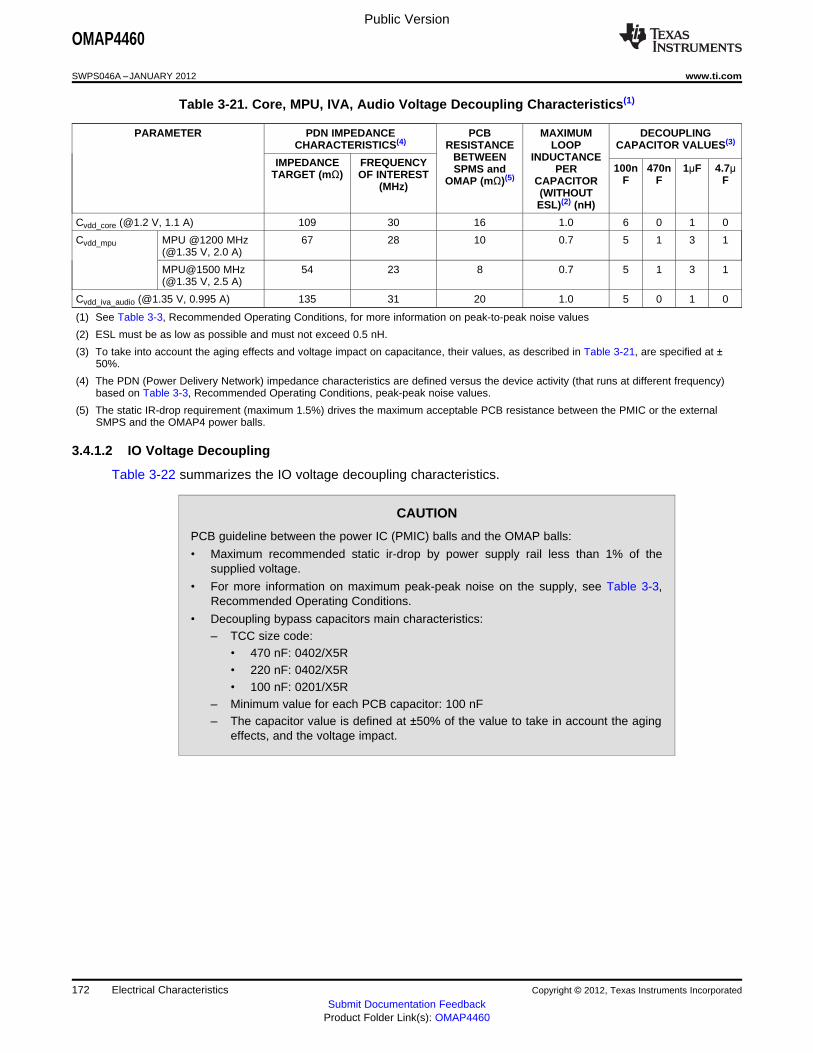
Public Version
OMAP4460
SWPS046A –JANUARY 2012 www.ti.com
Table 3-21. Core, MPU, IVA, Audio Voltage Decoupling Characteristics(1)
PARAMETER PDN IMPEDANCE PCB MAXIMUM DECOUPLINGCHARACTERISTICS(4) RESISTANCE LOOP CAPACITOR VALUES(3)
BETWEEN INDUCTANCEIMPEDANCE FREQUENCY 100n 470n 1µF 4.7µSPMS and PERTARGET (mΩ) OF INTEREST F F FOMAP (mΩ)(5) CAPACITOR(MHz)(WITHOUTESL)(2) (nH)
Cvdd_core (@1.2 V, 1.1 A) 109 30 16 1.0 6 0 1 0
Cvdd_mpu MPU @1200 MHz 67 28 10 0.7 5 1 3 1(@1.35 V, 2.0 A)
MPU@1500 MHz 54 23 8 0.7 5 1 3 1(@1.35 V, 2.5 A)
Cvdd_iva_audio (@1.35 V, 0.995 A) 135 31 20 1.0 5 0 1 0
(1) See Table 3-3, Recommended Operating Conditions, for more information on peak-to-peak noise values
(2) ESL must be as low as possible and must not exceed 0.5 nH.
(3) To take into account the aging effects and voltage impact on capacitance, their values, as described in Table 3-21, are specified at ±50%.
(4) The PDN (Power Delivery Network) impedance characteristics are defined versus the device activity (that runs at different frequency)based on Table 3-3, Recommended Operating Conditions, peak-peak noise values.
(5) The static IR-drop requirement (maximum 1.5%) drives the maximum acceptable PCB resistance between the PMIC or the externalSMPS and the OMAP4 power balls.
3.4.1.2 IO Voltage Decoupling
Table 3-22 summarizes the IO voltage decoupling characteristics.
CAUTION
PCB guideline between the power IC (PMIC) balls and the OMAP balls:
• Maximum recommended static ir-drop by power supply rail less than 1% of thesupplied voltage.
• For more information on maximum peak-peak noise on the supply, see Table 3-3,Recommended Operating Conditions.
• Decoupling bypass capacitors main characteristics:– TCC size code:
• 470 nF: 0402/X5R• 220 nF: 0402/X5R• 100 nF: 0201/X5R
– Minimum value for each PCB capacitor: 100 nF– The capacitor value is defined at ±50% of the value to take in account the aging
effects, and the voltage impact.
172 Electrical Characteristics Copyright © 2012, Texas Instruments Incorporated
Submit Documentation FeedbackProduct Folder Link(s): OMAP4460

Public Version
OMAP4460
www.ti.com SWPS046A –JANUARY 2012
Table 3-22. IO Voltage Decoupling Characteristics(1)(2)
PARAMETER MIN(4) TYP MAX(4) UNIT
1.2-V Supply Voltage IOs
Cvdds_1p2v 50 100 150 nF
1.8-V Supply Voltage IOs
Cvdds_1p8v 100 220 300 nF
Cvdds_1p8_fref 50 100 150
1.2-V, 1.8-V Supply Voltage IOs
Cvdds_dv_gpmc 300 6 x 100 900 nF
Cvdds_dv_sdmmc2
Cvdds_dv_c2c
Cvdds_dv_cam
Cvdds_dv_bank0
Cvdds_dv_bank1
Cvdds_dv_bank2
Cvdds_dv_bank3
Cvdds_dv_bank4
Cvdds_dv_bank5
Cvdds_dv_bank6
Cvdds_dv_bank7
Cvdds_dv_fref
1.8-V, 3.3-V SDMMC1 and SIM Supply Voltage IOs
Cvdds_usim 50 100 150 nF
Cvdds_sdmmc1 50 100 150 nF
1.2-V LPDDR2 Supply Voltage IOs
Cvddq_lpddr2 800 2 x 470 + 6 x 100 2400 nF
Cvddq_vref_lpddr2(3) 50 100 150 nF
Cvddca_lpddr2 285 1 x 100 + 1 x 470 855 nF
Cvddca_vref_lpddr2(3) 50 100 150 nF
Other
vpp_cust(5) 100 nF
(1) All capacitor values described in this table are based on capacitors of 100 nF.
(2) See Table 3-3 for more information on peak-to-peak noise values.
(3) vddq_vref_lpddr2 and vddca_vref_lpddr2 are dedicated power supplies for OMAP embedded VREF generator.
(4) To take into account the aging effects and voltage impact on capacitance, their values, as described in Table 3-22, are specified at ±50%.
(5) vpp_cust is only powered when programming CPFROM eFuses. Otherwise, it is recommended to leave vpp_cust turned off (floating).
Note that if the TWL6030 PMIC is used then the vpp pull-down resistor inside the TWL6030 must be disabled when vpp_cust is turnedoff.
Copyright © 2012, Texas Instruments Incorporated Electrical Characteristics 173Submit Documentation Feedback
Product Folder Link(s): OMAP4460

Public Version
OMAP4460
SWPS046A –JANUARY 2012 www.ti.com
3.4.1.3 Analog Voltage Decoupling
3.4.1.3.1 Analog Voltage Decoupling Values
Table 3-23 summarizes the analog voltage decoupling characteristics.
CAUTION
PCB guidelines between the power IC (PMIC) balls and the OMAP balls:
• Maximum recommended inductance (VDDA + VSSA) by power supply rail less than 30nH.
• The capacitors must be placed as closed as possible to the balls. Maximum loopinductance for the decoupling capacitances must not exceed:– 1.0 nH maximum for DLLs– 1.5 nH maximum for complex IOs (HDMI) and DPLLs– 2.0 nH maximum for SRAM LDOs, BodyBias (BB) LDOs, WakeUp (WKUP) LDO,
BandGap (BG) LDO, CSI2, CCPV2, and DSI
• Maximum recommended resistance (VDDA + VSSA) by power supply rail between 0.1Ω to 0.3 Ω.
• For more information on HDMI routing guidelines, see Figure 3-3, HDMI Power PCBRouting Topology.
• For more information on DPLLs and complex IOs routing guidelines, see Figure 3-4,DPLLs / Complex I/O VDDA Power PCB Routing Topology.
• For more information on OMAP4 embedded LDOs and BandGap routing guidelines,see Figure 3-5, OMAP Embedded LDO / Bandgap Power PCB Routing Topology.
Table 3-23. Analog Voltage Decoupling Characteristics(1)(2)
PARAMETER MIN(3) TYP MAX(3) UNIT
Cvdda_dpll_mpu 50 100 150 nF
Cvdda_dpll_core_audio 50 100 150 nF
Cvdda_dpll_iva_per 50 100 150 nF
Cvdda_dll0_lpddr21(4) 150 3 x 100 450 nF
Cvdda_dll1_lpddr21(4) nF
Cvdda_dll0_lpddr22(4) nF
Cvdda_dll1_lpddr22(4) nF
Cvdda_ldo_sram_mpu 110 220 330 nF
Cvdda_ldo_sram_iva_audio 110 220 330 nF
Cvdda_ldo_sram_core 110 220 330 nF
Cvdda_ldo_emu_wkup 50 100 150 nF
Cvdda_bdgp_vbb 50 100 150 nF
Cvdda_dsi1 110 220 330 nF
Cvdda_dsi2 110 220 330 nF
Cvdda_csi21 110 220 330 nF
Cvdda_csi22 110 220 330 nF
Cvdda_hdmi_vdac 235 470 705 nF
Cvdda_usba0otg_1p8v 110 220 330 nF
Cvdda_usba0otg_3p3v 110 220 330 nF
174 Electrical Characteristics Copyright © 2012, Texas Instruments Incorporated
Submit Documentation FeedbackProduct Folder Link(s): OMAP4460

11)P
TWL6030
IVDAC (ball G15)
OMAP4
P vdda_hdmi_vdac (ball A11)
11)PP vdda_hdmi_vdac (ball G12)
1µF 470 nF
SWPS042-006
Public Version
OMAP4460
www.ti.com SWPS046A –JANUARY 2012
(1) Decoupling capacitance side code (TCC): 0402/X5R.
(2) See Table 3-3 for more information on peak-to-peak noise values.
(3) To take into account the aging effects and voltage impact on capacitance, their values, as described in Table 3-23, are specified at±50%.
(4) In Figure 3-6 and Figure 3-7, External Capacitors, the three DLL decoupling capacitors have the names: Cvdda_dll1/3, Cvdda_dll2/3, andCvdda_dll3/3 to represent the three decoupling capacitors above the four power rails: vdda_dll0_lpddr21, vdda_dll1_lpddr21,vdda_dll0_lpddr22, and vdda_dll1_lpddr22.
3.4.1.3.2 Analog Voltage Decoupling—Example Of HDMI Routing Guidelines
The VDAC LDO within the TWL6030 PMIC device supplies the HDMI (vdda_hdmi_vdac OMAP4 powerpin) circuitry within the OMAP4 device. This power rail must be routed as a power trace from the LDOwhere it is star-routed to OMAP as shown in Figure 3-3, HDMI Power PCB Routing Topology.
For each power trace between the TWL6030 PMIC device and OMAP4 vdda_hdmi_vdac:• Maximum recommended resistance (VDDA + VSSA) by power supply rail must be 0.3 Ω.• Maximum recommended inductance by power supply rail less than 2 nH (VDD + VSS) must be 30 nH
Each decoupling capacitor must be located as close as possible to the OMAP4 power balls to reduce thedecoupling capacitor loop inductance:• Maximum loop inductance for the decoupling capacitors must not exceed:
– HDMI: less than 1.5 nH between their location on trace and the devices power balls
Figure 3-3. HDMI Power PCB Routing Topology
3.4.1.3.3 Analog Voltage Decoupling—Example Of VCXIO and VUSB Routing Guidelines
This section provides an example of VCXIO and VUSB routing guidelines based on a TWL6030 PMIC.
The TWL6030 PMIC power companion provides an LDO (VCXIO) that is used to power the DPLLs withinthe OMAP4 device, as well as the VDDA inputs to the complex I/O cells (except HDMI) used within theOMAP4.
Another LDO VUSB provides the 3.3-V supply for the USBPHY (to the OMAP4 vdda_usba0otg_3p3vpower pin).
Both LDOs must be routed as a power trace and star-routed to the OMAP4 as shown in Figure 3-4,DPLLs / Complex I/Os VDDA Power PCB Routing Topology.
For each power trace between TWL6030 PMIC device and the DPLLs, complex IOs power balls:• Maximum recommended resistance (VDDA + VSSA) by power supply rail must be 0.3 Ω.• Maximum recommended inductance by power supply rail less than 2 nH (VDD + VSS) must be 30 nH
Each decoupling capacitor must be located as close as possible to the OMAP4 power balls to reduce thedecoupling capacitor loop inductance:• Maximum loop inductance for the decoupling capacitors must not exceed:
– Complex IOs: less than 2 nH between their location on trace and the device power balls– DPLLs: less than 1.5 nH between their location on trace and the devices power balls
Copyright © 2012, Texas Instruments Incorporated Electrical Characteristics 175Submit Documentation Feedback
Product Folder Link(s): OMAP4460
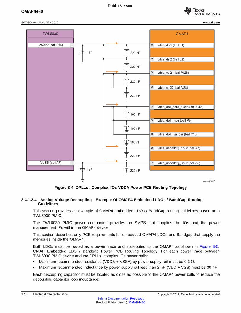
11)P
TWL6030
IVCXIO (ball F15)
OMAP4
P vdda_dsi1 (ball L1)
220 nF
11)PP
11)PP
vdda_dpll_core_audio (ball G13)
11)PP vdda_dpll_mpu (ball P9)
11)PP vdda_dpll_iva_per (ball Y16)
11)PP vdda_usba0otg_1p8v (ball A7)
11)PPIVUSB (ball A7)
1 µF
220 nF
220 nF
220 nF
100 nF
100 nF
11)PP
100 nF
220 nF
220 nF
vdda_dsi2 (ball L2)
vdda_csi21 (ball W28)
vdda_csi22 (ball V28)
vdda_usba0otg_3p3v (ball A5)
1 µF
swps042-007
11)PP
Public Version
OMAP4460
SWPS046A –JANUARY 2012 www.ti.com
Figure 3-4. DPLLs / Complex I/Os VDDA Power PCB Routing Topology
3.4.1.3.4 Analog Voltage Decoupling—Example Of OMAP4 Embedded LDOs / BandGap RoutingGuidelines
This section provides an example of OMAP4 embedded LDOs / BandGap routing guidelines based on aTWL6030 PMIC.
The TWL6030 PMIC power companion provides an SMPS that supplies the IOs and the powermanagement IPs within the OMAP4 device.
This section describes only PCB requirements for embedded OMAP4 LDOs and Bandgap that supply thememories inside the OMAP4.
Both LDOs must be routed as a power trace and star-routed to the OMAP4 as shown in Figure 3-5,OMAP Embedded LDO / Bandgap Power PCB Routing Topology. For each power trace betweenTWL6030 PMIC device and the DPLLs, complex IOs power balls:• Maximum recommended resistance (VDDA + VSSA) by power supply rail must be 0.3 Ω.• Maximum recommended inductance by power supply rail less than 2 nH (VDD + VSS) must be 30 nH
Each decoupling capacitor must be located as close as possible to the OMAP4 power balls to reduce thedecoupling capacitor loop inductance:
176 Electrical Characteristics Copyright © 2012, Texas Instruments Incorporated
Submit Documentation FeedbackProduct Folder Link(s): OMAP4460
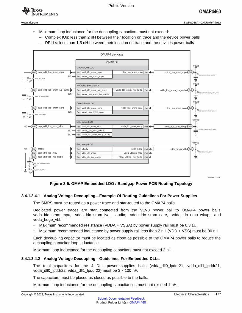
OMAP die
1 µF
11)PPad
11)PPad
vdda_ldo_sram_mpu
vnwa_ldo_sram_mpu
cap_vdd_ldo_sram_mpu 11)PPad vdd_ldo_sram_mpu
NC
MPU SRAM LDO
vdda_ldo_sram_mpuCVDDA_LDO_SRAM_MPU_OMAP
11)PPad
11)PPad vnwa_ldo_sram_iva_audio
11)PPad vdd_ldo_sram_iva_audio
IVA Audio SRAM LDO
vdda_ldo_sram_iva_audioCVDDA_LDO_SRAM_IVA_AUDIO_OMAP
V1V8
V1V8
vdda_ldo_sram_iva_audio
1 µF
cap_vdd_ldo_sram_iva_audio
NC
11)PPad
11)PPad vnwa_ldo_sram_core
11)PPad vdd_ldo_sram_core
Core SRAM LDO
vdda_ldo_sram_coreCVDDA_LDO_SRAM_CORE_OMAP
V1V8
vdda_ldo_sram_core
1 µF
cap_vdd_ldo_sram_core
NC
11)PPad vnwa_ldo_emu_wkup
11)PPad vdd_ldo_emu_wkup
Emu Wkup LDO
vdda_ldo_emu_wkupCVDDA_LDO_EMU_WKUP_OMAP
V1V29
vdda_ldo_emu_wkupcap_vdd_ldo_emu_wkup
NC
NC
11)PPadNC vdda_ldo_emu_wkup_array
11)PPad
11)PPad vbb_ldo_mpu
11)PPad atestv
Emu Wkup LDO
vdda_bdgp_vbbCVDDA_BDGP_VBB_OMAP
V1V28
vdda_bdgpatestvNC
11)PPad vbb_ldo_iva_audio
11)PPad
cap_vbb_ldo_mpu
cap_vbb_ldo_iva_audio
1 µF
vdda_vbbido_mpu 11)PPad
vdda_vbbldo_iva_audio 11)PPad
CVDD_LDO_SRAM_MPU_OMAP
CVDD_LDO_SRAM_IVA_AUDIO_OMAP
CVDD_LDO_SRAM_CORE_OMAP
1 µF
CVBB_LDO_IVA_AUDIO_OMAP
CVBB_LDO_IVA_AUTO_OMAP
Ball
Ball
Ball
Ball
Ball
Ball
Ball
Ball
Ball
Ball
Ball
Ball
SWPS042-008
OMAP4 package
Public Version
OMAP4460
www.ti.com SWPS046A –JANUARY 2012
• Maximum loop inductance for the decoupling capacitors must not exceed:– Complex IOs: less than 2 nH between their location on trace and the device power balls– DPLLs: less than 1.5 nH between their location on trace and the devices power balls
Figure 3-5. OMAP Embedded LDO / Bandgap Power PCB Routing Topology
3.4.1.3.4.1 Analog Voltage Decoupling—Example Of Routing Guidelines For Power Supplies
The SMPS must be routed as a power trace and star-routed to the OMAP4 balls.
Dedicated power traces are star connected from the V1V8 power ball to OMAP4 power ballsvdda_ldo_sram_mpu, vdda_ldo_sram_iva_ audio, vdda_ldo_sram_core, vdda_ldo_emu_wkup, andvdda_bdgp_vbb:• Maximum recommended resistance (VDDA + VSSA) by power supply rail must be 0.3 Ω.• Maximum recommended inductance by power supply rail less than 2 nH (VDD + VSS) must be 30 nH.
Each decoupling capacitor must be located as close as possible to the OMAP4 power balls to reduce thedecoupling capacitor loop inductance.
Maximum loop inductance for the decoupling capacitors must not exceed 2 nH.
3.4.1.3.4.2 Analog Voltage Decoupling—Guidelines For Embedded DLLs
The total capacitors for the 4 DLL power supplies balls (vdda_dll0_lpddr21, vdda_dll1_lpddr21,vdda_dll0_lpddr22, vdda_dll1_lpddr22) must be 3 x 100 nF.
The capacitors must be placed as closed as possible to the balls.
Maximum loop inductance for the decoupling capacitances must not exceed 1 nH.
Copyright © 2012, Texas Instruments Incorporated Electrical Characteristics 177Submit Documentation Feedback
Product Folder Link(s): OMAP4460
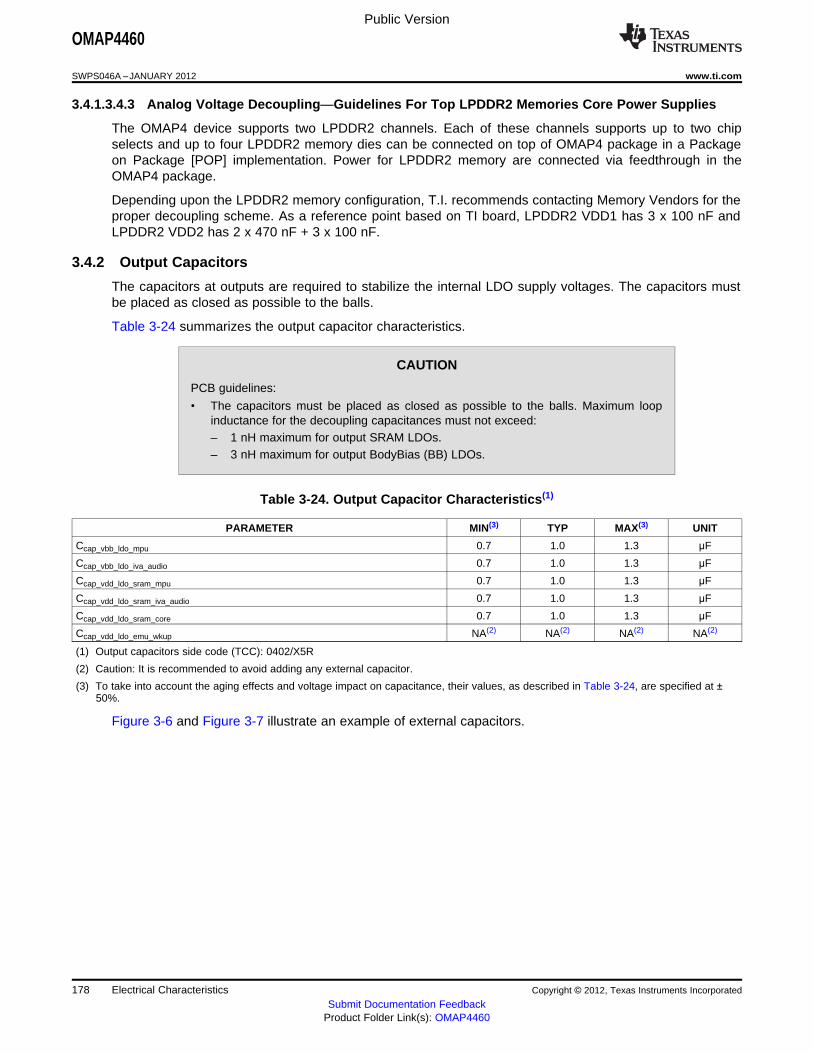
Public Version
OMAP4460
SWPS046A –JANUARY 2012 www.ti.com
3.4.1.3.4.3 Analog Voltage Decoupling—Guidelines For Top LPDDR2 Memories Core Power Supplies
The OMAP4 device supports two LPDDR2 channels. Each of these channels supports up to two chipselects and up to four LPDDR2 memory dies can be connected on top of OMAP4 package in a Packageon Package [POP] implementation. Power for LPDDR2 memory are connected via feedthrough in theOMAP4 package.
Depending upon the LPDDR2 memory configuration, T.I. recommends contacting Memory Vendors for theproper decoupling scheme. As a reference point based on TI board, LPDDR2 VDD1 has 3 x 100 nF andLPDDR2 VDD2 has 2 x 470 nF + 3 x 100 nF.
3.4.2 Output Capacitors
The capacitors at outputs are required to stabilize the internal LDO supply voltages. The capacitors mustbe placed as closed as possible to the balls.
Table 3-24 summarizes the output capacitor characteristics.
CAUTION
PCB guidelines:
• The capacitors must be placed as closed as possible to the balls. Maximum loopinductance for the decoupling capacitances must not exceed:– 1 nH maximum for output SRAM LDOs.– 3 nH maximum for output BodyBias (BB) LDOs.
Table 3-24. Output Capacitor Characteristics(1)
PARAMETER MIN(3) TYP MAX(3) UNIT
Ccap_vbb_ldo_mpu 0.7 1.0 1.3 µF
Ccap_vbb_ldo_iva_audio 0.7 1.0 1.3 µF
Ccap_vdd_ldo_sram_mpu 0.7 1.0 1.3 µF
Ccap_vdd_ldo_sram_iva_audio 0.7 1.0 1.3 µF
Ccap_vdd_ldo_sram_core 0.7 1.0 1.3 µF
Ccap_vdd_ldo_emu_wkup NA(2) NA(2) NA(2) NA(2)
(1) Output capacitors side code (TCC): 0402/X5R
(2) Caution: It is recommended to avoid adding any external capacitor.
(3) To take into account the aging effects and voltage impact on capacitance, their values, as described in Table 3-24, are specified at ±50%.
Figure 3-6 and Figure 3-7 illustrate an example of external capacitors.
178 Electrical Characteristics Copyright © 2012, Texas Instruments Incorporated
Submit Documentation FeedbackProduct Folder Link(s): OMAP4460

OMAP4 Device
DPLL PER
DPLL IVAvdda_dpll_iva_per
vdda_dpll_iva_per
Cvdda_dpl_iva_per
GPMC DV IOvdds_dv_gpmcvdds_dv_gpmc
C2C DV IOvdds_dv_c2c
vdds_dv_c2c
CAM DV IOvdds_dv_cam
vdds_dv_cam
MPU VBBLDO
vdda_bdgp_vbb
MPU SRAMLDO
vdda_ldo_sram_mpuvdda_ldo_sram_mpu
SERIALBANK5 DV IO
vdds_dv_bank5vdds_dv_bank5
SERIALBANK0 DV IO
vdds_dv_bank0vdds_dv_bank0
SERIALBANK1 DV IO
vdds_dv_bank1vdds_dv_bank1
SERIALBANK2 DV IO
vdds_dv_bank2vdds_dv_bank2
vdds_dv_bank3vdds_dv_bank3
SERIALBANK4 DV IO
vdds_dv_bank4vdds_dv_bank4
BandgapLDO
IVA AudioVBB LDO
vdda_bdgp_vbb
Cvdda_bdgp_vbb
Cvdda_ldo_sram_mpu
FREF DV IOvdds_dv_fref
vdds_dv_fref
SERIALBANK6 DV IO
vdds_dv_bank6vdds_dv_bank6
DPLL COREvdda_dpll_core_audio
vdda_dpll_core_audio
Cvdda_dpll_core_audio
IVAvdd_iva_audio
vdd_iva_audio
Audio BE
MPUvdd_mpu
Ccap_vbb_ldo_mpu
Ccap_vbb_ldo_iva_audio
vdd_mpu
Ccap_vdd_ldo_sram_mpu
IVA AudioSRAM LDO
vdda_ldo_sram_iva_audio vdda_ldo_sram_iva_audio
Cvdda_ldo_sram_iva_audio
Ccap_vdd_ldo_sram_iva_audio
CORE SRAMLDO
vdda_ldo_sram_corevdda_ldo_sram_core
Cvdda_ldo_sram_core
Ccap_vdd_ldo_sram_core
WKUP EMULDO
vdda_ldo_emu_wkup vdda_ldo_emu_wkup
Cvdda_ldo_emu_wkup
WKUP EMUArray LDO
SERIALBANK3 DV IO
SERIALBANK7 DV IO
vdds_dv_bank7vdds_dv_bank7
SWPS040-001A
DPLL AUDIO
See(2)
See(2)
See(2)
See(2)
See(2)
See(2)
See(2)
See(2)
See(2)
See(2)
See(2)
See(2)
See(1)
See(1)
Public Version
OMAP4460
www.ti.com SWPS046A –JANUARY 2012
Figure 3-6. External Capacitors—Page 1 of 2(1)(2)
(1) The vdd_mpu, vdd_iva_audio and vdd_core decoupling capacitors placement depends on the board layout. The recommended numberof decoupling capacitors is described in Table 3-21, Core, MPU, IVA, Audio Voltage Decoupling Characteristics.
(2) The decoupling capacitors placement of the gpmc, sdmmc2, c2c, cam, bank[7:0], fref VDDS dual voltages (dv) depends on the boardlayout. The number of decoupling capacitors to be used is described in Table 3-22, IO Voltage Decoupling Characteristics. Regardingthe vddq_vref_lpddr2 and vddca_vref_lpddr2 decoupling capacitors requirement, see also Table 3-22, IO Voltage DecouplingCharacteristics.
Copyright © 2012, Texas Instruments Incorporated Electrical Characteristics 179Submit Documentation Feedback
Product Folder Link(s): OMAP4460
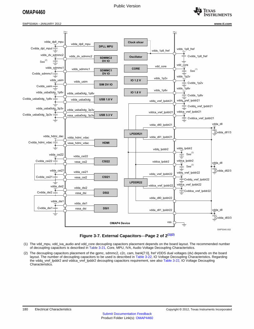
SWPS045-002
OMAP4 Device
COREvdd_core
vdd_core
vddq_vref_lpddr22
vddq_lpddr2
LPDDR22
vddq_lpddr2
vddq_vref_lpddr22
vddca_vref_lpddr22 vddca_vref_lpddr22
vddca_lpddr2 vddca_lpddr2
vdda_dll0_lpddr22
vdda_dll1_lpddr22vssa_dsi
vdda_dsi1
Cvdda_dsi1
vssa_dsi
vdda_dsi2
Cvdda_dsi2
vssa_csi2
vdda_csi21
Cvdda_csi21
vssa_csi2
vdda_csi22
Cvdda_csi22
vssa_hdmi_vdac
vdda_hdmi_dac
Cvdda_hdmi_vdac
vssa_usba0otg_3p3v
vdda_usba0otg_3p3v
Cvdda_usba0otg_3p3v
vdda_usba0otg
vdda_usba0otg_1p8v
Cvdda_usba0otg_1p8v
vdda_dsi1
vdda_dsi2
vdda_csi21
vdda_csi22
vdda_hdmi_vdac
vdda_usba0otg_3p3v
vdda_usba0otg_1p8v
vdds_usimvdds_usim
Cvdds_usim
vdda_dpll_mpuvdda_dpll_mpu
Cvdda_dpl_mpul
vdds_dv_sdmmc2vdds_dv_sdmmc2
Cvddca_vref_lpddr22
Cvddq_vref_lpddr22
vss
Clock slicer
vdds_sdmmc1vdds_sdmmc1
Cvdds_sdmmc1
vddq_vref_lpddr21
LPDDR21
vddq_vref_lpddr21
vddca_vref_lpddr21 vddca_vref_lpddr21
vdda_dll0_lpddr21 vdda_dll
vdda_dll1_lpddr21
Cvdda_dll1/3
Cvddq_vref_lpddr21
Oscillator
vdds_1p8_frefvdds_1p8_fref
Cvdds_1p8_fref
IO 1.8 Vvdds_1p8v
vdds_1p8v
Cvdds_1p8v
IO 1.2 Vvdds_1p2v
vdds_1p2v
Cvdds_1p2v
Cvddca_vref_lpddr21
HDMI
USB 3.3 V
USB 1.8 V
SIM DV IO
DPLL MPU
SDMMC2
DV IO
SDMMC1
DV IO
DSI1
DSI2
CSI21
CSI22
See(2)
See(1)
See(2)
See(2)
vdda_dll
Cvdda_dll3/3
vdda_dll
Cvdda_dll2/3
Public Version
OMAP4460
SWPS046A –JANUARY 2012 www.ti.com
Figure 3-7. External Capacitors—Page 2 of 2(1)(2)
(1) The vdd_mpu, vdd_iva_audio and vdd_core decoupling capacitors placement depends on the board layout. The recommended numberof decoupling capacitors is described in Table 3-21, Core, MPU, IVA, Audio Voltage Decoupling Characteristics.
(2) The decoupling capacitors placement of the gpmc, sdmmc2, c2c, cam, bank[7:0], fref VDDS dual voltages (dv) depends on the boardlayout. The number of decoupling capacitors to be used is described in Table 3-22, IO Voltage Decoupling Characteristics. Regardingthe vddq_vref_lpddr2 and vddca_vref_lpddr2 decoupling capacitors requirement, see also Table 3-22, IO Voltage DecouplingCharacteristics.
180 Electrical Characteristics Copyright © 2012, Texas Instruments Incorporated
Submit Documentation FeedbackProduct Folder Link(s): OMAP4460
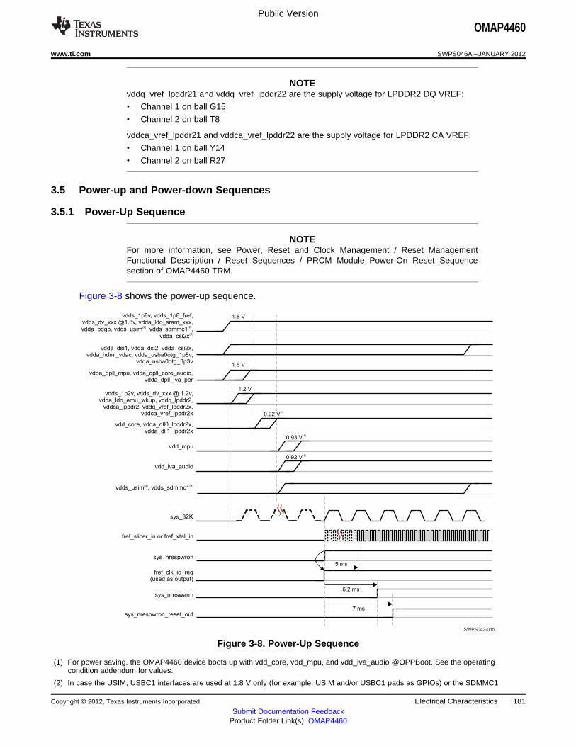
1.8 V
1.2 V
0.92 V(1)
6.2 ms
7 ms
5 ms
vdds_1p8v, vdds_1p8_fref,vdds_dv_xxx @1.8v, vdda_ldo_sram_xxx,vdda_bdgp, vdds_usim , vdds_sdmmc1 ,
vdda_csi2x
(2) (2)
(2)
vdda_dsi1, vdda_dsi2, vdda_csi2x,vdda_hdmi_vdac, vdda_usba0otg_1p8v,
vdda_usba0otg_3p3v
vdda_dpll_mpu, vdda_dpll_core_audio,vdda_dpll_iva_per
vdds_1p2v, vdds_dv_xxx @ 1.2v,vdda_ldo_emu_wkup, vddq_lpddr2,
vddca_lpddr2, vddq_vref_lpddr2x,vddca_vref_lpddr2x
vdd_core, vdda_dll0_lpddr2x,vdda_dll1_lpddr2x
vdd_mpu
vdd_iva_audio
vdds_usim , vdds_sdmmc1(3) (3)
sys_32K
fref_slicer_in or fref_xtal_in
sys_nreswarm
sys_nrespwron
fref_clk_io_req(used as output)
sys_nrespwron_reset_out
1.8 V
0.93 V(1)
0.92 V(1)
SWPS042-015
Public Version
OMAP4460
www.ti.com SWPS046A –JANUARY 2012
NOTEvddq_vref_lpddr21 and vddq_vref_lpddr22 are the supply voltage for LPDDR2 DQ VREF:
• Channel 1 on ball G15
• Channel 2 on ball T8
vddca_vref_lpddr21 and vddca_vref_lpddr22 are the supply voltage for LPDDR2 CA VREF:
• Channel 1 on ball Y14
• Channel 2 on ball R27
3.5 Power-up and Power-down Sequences
3.5.1 Power-Up Sequence
NOTEFor more information, see Power, Reset and Clock Management / Reset ManagementFunctional Description / Reset Sequences / PRCM Module Power-On Reset Sequencesection of OMAP4460 TRM.
Figure 3-8 shows the power-up sequence.
Figure 3-8. Power-Up Sequence
(1) For power saving, the OMAP4460 device boots up with vdd_core, vdd_mpu, and vdd_iva_audio @OPPBoot. See the operatingcondition addendum for values.
(2) In case the USIM, USBC1 interfaces are used at 1.8 V only (for example, USIM and/or USBC1 pads as GPIOs) or the SDMMC1
Copyright © 2012, Texas Instruments Incorporated Electrical Characteristics 181Submit Documentation Feedback
Product Folder Link(s): OMAP4460
Public Version
OMAP4460
SWPS046A –JANUARY 2012 www.ti.com
interface is used at 1.8 V only (for example, as GPIOs or for SDIO device or eMMC device…) or the CSI2 interfaces are used as GPIs.
(3) In case the USIM, USBC1, SDMMC1 functional signals are used at 1.8 V / 3.0 V.
NOTEWhen supplied at 1.8 V, the vdds_dv_xxx dual-voltage supplies (xxx represents bank[7:0],gpmc, sdmmc2, c2c, cam, fref) must be turned on before the one supplied at 1.2 V. Onlyexception is vdds_dv_c2c that can be turned on at any time (including after OMAP boot),whatever its voltage.
Inside a vdds_dv group @1.8 V or @ 1.2 V, each vdds_dv_xxx voltage supply can be turnedon any time compared with the other vdds_dv_xxx voltage supplies.
The vdda_dpll_xxx voltage supplies can be turned on at the same time as the other 1.8-Vvoltage supplies.
The 1.8-V and 3.3-V PHY voltage supplies can be turned on at the same time as the other1.8-V voltage supplies or only when the corresponding applications are needed.
Once vdda_ldo_emu_wkup is turned on, vdd_core can be turned on. Once vdd_core isturned on, vdd_mpu and vdd_iva_audio can be turned on.
If the USIM, USBC1, SDMMC1 functional signals are used at 1.8 V / 3.0 V, the vdds_usim,vdds_sdmmc1 voltage supplies can be turned on any time after vdd_core ramp-up or onlywhen the applications are needed.
sys_32k can be turned on any time between vdds_1p8v ramp-up and sys_nrespwronrelease.
Once the sys_nrespwron is released, OMAP4460 activates the fref_clk_io_req signal.Therefore, the fref_slicer_in or fref_xtal_in clock can be turned on. (Nevertheless, the systemcan turn on the fref_slicer_in or fref_xtal_in clock before the fref_clk_io_req activationprovided the vdds_1p8v supply is on.)
5 ms after the sys_nrespwron release, the clock is considered as stabilized on theOMAP4460 slicer input or crystal input. The clock may be supplied later provided it isperfectly stabilized when supplied.
1.2 ms (about 40 additional 32-kHz clock cycles) after the clock is considered as stabilized,OMAP4460 releases its sys_nreswarm.
2 ms after the clock is considered as stabilized, OMAP4460 activates the sys_pwron_reset_out signal.
3.5.2 Power-Down Sequence
The following steps give two examples of power-down sequence supported by the OMAP4460 device.
1. Put the OMAP4460 device under reset (sys_nrespwron)
2. Stop all signals driven to its balls (sys_32k, fref_slicer_in or fref_xtal_in)
3. Either:
(a) Shutdown all power domains at once. This sequence is described in black color in Figure 3-9.(b) Or, if the shutdown is sequenced, you must follow these steps (described in dashed blue color in
Figure 3-9):(i) Turn off all PHY power supplies and SIM/SDMMC1 IO power supplies(ii) Turn off the IVA and AUDIO domains power supplies(iii) Turn off the MPU domain power supply(iv) Turn off the CORE domain power supply and all DLL power supplies(v) Turn off all DPLL power supplies(vi) Turn off all 1.2-V IO power supplies(vii) Turn off all 1.8-V IO power supplies
182 Electrical Characteristics Copyright © 2012, Texas Instruments Incorporated
Submit Documentation FeedbackProduct Folder Link(s): OMAP4460

SWPS040-003
vdd_core, vdda_dll0_lpddr2x,
vdda_dll1_lpddr2x
sys_nrespwron
vdds_1p8v, vdds_1p8_fref, vdds_dv_xxx
@1.8v, vdda_ldo_sram_xxx, vdda_bdgp
vdds_1p2v, [email protected],
vdda_ldo_emu_wkup, vddq_lpddr2,
vddca_lpddr2, vddq_vref_lpddr2x
vddca_vref_lpddr2x
vdda_dpll_mpu, vdda_dpll_core_audio,
vdda_dpll_iva_per
vdd_mpu
vdd_iva_audio
sys_32K
fref_slicer_in or fref_xtal_in
vdda_dsi1, vdda_dsi2, vdda_csi2x,
vdda_hdmi_vdac, vdda_usba0otg_3p3v,
vdda_usba0otg_1p8v, vdds_usim,
vdds_sdmmc1
Public Version
OMAP4460
www.ti.com SWPS046A –JANUARY 2012
Figure 3-9 shows both power-down sequences: one of them is described in black color, and the other onein dashed blue color.
Figure 3-9. Power-Down Sequence
NOTEsys_32k can be turned off any time between sys_nrespwron assertion and vdds_1p8vshutdown.
fref_slicer_in or fref_xtal_in can be turned off any time between sys_nrespwron assertion andvdds_1p8v shutdown.
Copyright © 2012, Texas Instruments Incorporated Electrical Characteristics 183Submit Documentation Feedback
Product Folder Link(s): OMAP4460

Public Version
OMAP4460
SWPS046A –JANUARY 2012 www.ti.com
4 Clock Specifications
NOTEFor more information, see Power Reset and Clock Management / PRCM Environment /External Clock Signal section and Power Reset and Clock Management / Clock ManagerFunctional Description section of the OMAP4460 TRM.
The OMAP4460 device operation requires the following input clocks: 32-kHz clock (sys_32k) and eitherslicer clock (fref_slicer_in) or crystal clock (fref_xtal_in / fref_xtal_out). fref_slicer_in and fref_xtal_in /fref_xtal_out at the same time is not a possible configuration. Here is the description of the three inputclocks:• The sys_32k input clock (32-kHz) is used for low frequency operation. It supplies the wake-up domain
for operation in lowest power mode (off mode) and the clock source for the DPLL audio back-endDPLL.
• The fref_xtal_in input clock (12, 16.8, 19.2, 26, or 38.4 MHz) is used as a system input clock togenerate the source clock of the OMAP4460 device. It supplies the DPLLs as well as several OMAPmodules. The system input clock can be connected to either:– A crystal oscillator clock (12-MHz, 16.8-MHz, 19.2-MHz) managed by fref_xtal_in and fref_xtal_out.
In this case, the fref_clk_ioreq is used as an input (GPIN).– A CMOS digital clock through the fref_xtal_in pin. In this case, the fref_clk_ioreq is used as an
output to request the external system clock.– In these two cases, the fref_slicer_in input can be used to provide the OMAP4460 device with an
alternate input clock up to 38.4 MHz (for example, for the 27-MHz VENC clock).• The fref_slicer_in input clock (12-MHz, 16.8-MHz, 19.2-MHz, 26-MHz, and 38.4-MHz) is also used as a
system input clock to generate the source clock of the OMAP4460 device. It supplies the DPLLs aswell as several OMAP4460 modules. The system input clock can be connected to either:– A single-ended sine clock, through the fref_slicer_in pin, which is converted by the internal slicer to
a digital square clock. In this case, the fref_clk_ioreq is used an output to request the externalsystem clock.
– A CMOS digital clock through the fref_slicer_in pin. In this case, the fref_clk_ioreq is used as anoutput to request the external system clock.
– In these two cases, the fref_xtal_in input can be used to provide the OMAP4460 device with analternate input clock up to 100 MHz (for example, for the 54-MHz VENC clock).
The OMAP4460 outputs externally six clocks:• fref_clk1_out is specially targeted for the primary camera sensor functional input clock.• fref_clk2_out is for the secondary camera sensor functional input clock.• fref_clk0_out, fref_clk3_out, fref_clk4_out, and fref_clk5_out are also available to supply input clocks
for the other peripherals.
Each output clock source can be selected independently between the system clock (fref_xtal_in,fref_slicer_in), PER DPLL or CORE DPLL, with a programmable divider factor.
After the reset sequence, fref_clk4_out output clock is activated by default whatever the request level fromfref_clk4_req signal. fref_clk5_out output clock is active only if fref_clk4_out output clock is deactivated (norequest from fref_clk4_req signal). fref_clk1_out and fref_clk2_out output clocks are not always-on clocks.
Figure 4-1 shows the external input clock sources and the output clocks to peripherals.
184 Clock Specifications Copyright © 2012, Texas Instruments Incorporated
Submit Documentation FeedbackProduct Folder Link(s): OMAP4460
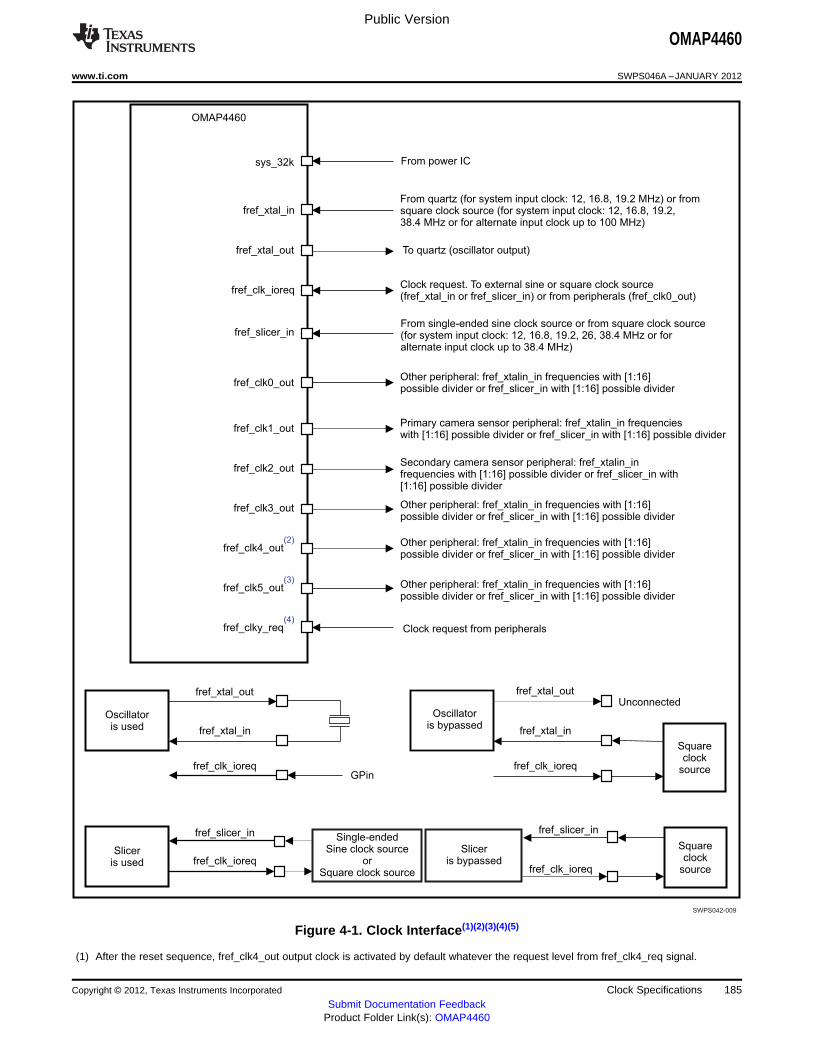
SWPS042-009
OMAP4460
sys_32k
fref_slicer_in
fref_clk0_out
From single-ended sine clock source or from square clock source(for system input clock: 12, 16.8, 19.2, 26, 38.4 MHz or foralternate input clock up to 38.4 MHz)
To quartz (oscillator output)
Clock request. To external sine or square clock source(fref_xtal_in or fref_slicer_in) or from peripherals (fref_clk0_out)
Oscillatoris used
Oscillatoris bypassed
Unconnected
GPin
Other peripheral: fref_xtalin_in frequencies with [1:16]possible divider or fref_slicer_in with [1:16] possible divider
fref_clky_req(4)
fref_xtal_out
fref_xtal_in
fref_clk_ioreq
fref_xtal_out
fref_xtal_in
fref_clk_ioreq
fref_xtal_out
fref_xtal_in
Squareclock
source
Sliceris used
fref_clk_ioreq
fref_slicer_in
Squareclock
sourcefref_clk_ioreq
Sliceris bypassed
fref_slicer_in
fref_clk_ioreq
Clock request from peripherals
fref_clk1_outPrimary camera sensor peripheral: fref_xtalin_in frequencieswith [1:16] possible divider or fref_slicer_in with [1:16] possible divider
fref_clk2_out
fref_clk3_out Other peripheral: fref_xtalin_in frequencies with [1:16]possible divider or fref_slicer_in with [1:16] possible divider
fref_clk4_out(2) Other peripheral: fref_xtalin_in frequencies with [1:16]
possible divider or fref_slicer_in with [1:16] possible divider
fref_clk5_out(3)
Other peripheral: fref_xtalin_in frequencies with [1:16]possible divider or fref_slicer_in with [1:16] possible divider
Secondary camera sensor peripheral: fref_xtalin_infrequencies with [1:16] possible divider or fref_slicer_in with[1:16] possible divider
From power IC
From quartz (for system input clock: 12, 16.8, 19.2 MHz) or fromsquare clock source (for system input clock: 12, 16.8, 19.2,38.4 MHz or for alternate input clock up to 100 MHz)
Single-endedSine clock source
orSquare clock source
Public Version
OMAP4460
www.ti.com SWPS046A –JANUARY 2012
Figure 4-1. Clock Interface(1)(2)(3)(4)(5)
(1) After the reset sequence, fref_clk4_out output clock is activated by default whatever the request level from fref_clk4_req signal.
Copyright © 2012, Texas Instruments Incorporated Clock Specifications 185Submit Documentation Feedback
Product Folder Link(s): OMAP4460
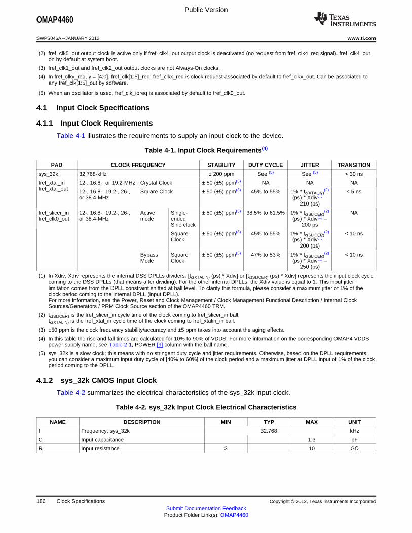
Public Version
OMAP4460
SWPS046A –JANUARY 2012 www.ti.com
(2) fref_clk5_out output clock is active only if fref_clk4_out output clock is deactivated (no request from fref_clk4_req signal). fref_clk4_outon by default at system boot.
(3) fref_clk1_out and fref_clk2_out output clocks are not Always-On clocks.
(4) In fref_clky_req, y = [4;0]. fref_clk[1:5]_req: fref_clkx_req is clock request associated by default to fref_clkx_out. Can be associated toany fref_clk[1:5]_out by software.
(5) When an oscillator is used, fref_clk_ioreq is associated by default to fref_clk0_out.
4.1 Input Clock Specifications
4.1.1 Input Clock Requirements
Table 4-1 illustrates the requirements to supply an input clock to the device.
Table 4-1. Input Clock Requirements(4)
PAD CLOCK FREQUENCY STABILITY DUTY CYCLE JITTER TRANSITION
sys_32k 32.768-kHz ± 200 ppm See (5) See (5) < 30 ns
fref_xtal_in 12-, 16.8-, or 19.2-MHz Crystal Clock ± 50 (±5) ppm(3) NA NA NAfref_xtal_out 12-, 16.8-, 19.2-, 26-, Square Clock ± 50 (±5) ppm(3) 45% to 55% 1% * tc(XTALIN)
(2) < 5 nsor 38.4-MHz (ps) * Xdiv(1) –
210 (ps)
fref_slicer_in 12-, 16.8-, 19.2-, 26-, Active Single- ± 50 (±5) ppm(3) 38.5% to 61.5% 1% * tc(SLICER)(2) NA
fref_clk0_out or 38.4-MHz mode ended (ps) * Xdiv(1) –Sine clock 200 ps
Square ± 50 (±5) ppm(3) 45% to 55% 1% * tc(SLICER)(2) < 10 ns
Clock (ps) * Xdiv(1) –200 (ps)
Bypass Square ± 50 (±5) ppm(3) 47% to 53% 1% * tc(SLICER)(2) < 10 ns
Mode Clock (ps) * Xdiv(1) –250 (ps)
(1) In Xdiv, Xdiv represents the internal DSS DPLLs dividers. [tc(XTALIN) (ps) * Xdiv] or [tc(SLICER) (ps) * Xdiv] represents the input clock cyclecoming to the DSS DPLLs (that means after dividing). For the other internal DPLLs, the Xdiv value is equal to 1. This input jitterlimitation comes from the DPLL constraint shifted at ball level. To clarify this formula, please consider a maximum jitter of 1% of theclock period coming to the internal DPLL (input DPLL).For more information, see the Power, Reset and Clock Management / Clock Management Functional Description / Internal ClockSources/Generators / PRM Clock Source section of the OMAP4460 TRM.
(2) tc(SLICER) is the fref_slicer_in cycle time of the clock coming to fref_slicer_in ball.tc(XTALIN) is the fref_xtal_in cycle time of the clock coming to fref_xtalin_in ball.
(3) ±50 ppm is the clock frequency stability/accuracy and ±5 ppm takes into account the aging effects.
(4) In this table the rise and fall times are calculated for 10% to 90% of VDDS. For more information on the corresponding OMAP4 VDDSpower supply name, see Table 2-1, POWER [9] column with the ball name.
(5) sys_32k is a slow clock; this means with no stringent duty cycle and jitter requirements. Otherwise, based on the DPLL requirements,you can consider a maximum input duty cycle of [40% to 60%] of the clock period and a maximum jitter at DPLL input of 1% of the clockperiod coming to the DPLL.
4.1.2 sys_32k CMOS Input Clock
Table 4-2 summarizes the electrical characteristics of the sys_32k input clock.
Table 4-2. sys_32k Input Clock Electrical Characteristics
NAME DESCRIPTION MIN TYP MAX UNIT
f Frequency, sys_32k 32.768 kHz
Ci Input capacitance 1.3 pF
Ri Input resistance 3 10 GΩ
186 Clock Specifications Copyright © 2012, Texas Instruments Incorporated
Submit Documentation FeedbackProduct Folder Link(s): OMAP4460

sys_32k
CK0 CK1 CK1
SWPS039-005
Crystal
Cf1 Cf2
fref_xtal_in fref_xtal_vssosc fref_xtal_out
OMAP4460 device
SWPS042-010
Public Version
OMAP4460
www.ti.com SWPS046A –JANUARY 2012
Table 4-3 details the input requirements of the sys_32k input clock.
Table 4-3. sys_32k Input Clock Timing Requirements(1)(2)
NAME DESCRIPTION MIN TYP MAX UNIT
CK0 1 / tc(32k) Frequency, sys_32k 32.768 kHz
tR(32k) Rise time, sys_32k 30 ns
tF(32k) Fall time, sys_32k 30 ns
tj(32k) Frequency stability, sys_32k 200 ppm
(1) See Table 3-20, System DC Electrical Characteristics, SYS (clk32k …) part for sys_32k VIH/VIL parameters.
(2) In this table the rise and fall times are calculated for 10% to 90% of VDDS. For more information on the corresponding OMAP4 VDDSpower supply name, see Table 2-1, POWER [9] column with the ball name.
Figure 4-2. sys_32k Input Clock
4.1.3 fref_xtalin CMOS Input Clock
4.1.3.1 fref_xtal_in / fref_xtal_out External Crystal
An external crystal is connected to the device pins. Figure 4-3 describes the crystal implementation.
Figure 4-3. Crystal Implementation(1)
(1) When the oscillator is bypassed, the fref_xtal_in ball is connected to a square clock source, the fref_xtal_out ball is not connected andthe fref_xtal_vssosc ball is connected to the ground.
When the oscillator is not used, the fref_xtal_in and fref_xtal_out balls can be connected to the ground or not connected and thefref_xtal_vssosc ball is connected to the ground.
The crystal must be in the fundamental mode of operation and parallel resonant. Table 4-4 summarizesthe required electrical constraints.
Table 4-4. Crystal Electrical Characteristics(2)
NAME DESCRIPTION MIN TYP MAX UNIT
fp Parallel resonance crystal frequency 12, 16.8, or 19.2 MHz
Cf1 Cf1 load capacitance for crystal parallel resonance with Cf1 = Cf2 12 24 pF
Cf2 Cf2 load capacitance for crystal parallel resonance with Cf1 = Cf2 12 24 pF
Copyright © 2012, Texas Instruments Incorporated Clock Specifications 187Submit Documentation Feedback
Product Folder Link(s): OMAP4460
Public Version
OMAP4460
SWPS046A –JANUARY 2012 www.ti.com
Table 4-4. Crystal Electrical Characteristics(2) (continued)
NAME DESCRIPTION MIN TYP MAX UNIT
ESR(Cf1,Cf2)(1) Frequency 12 MHz, Negative resistor at nominal 500 Ω, Negative 100 Ωresistor at worst case 300 ΩFrequency 16.8 MHz and 19.2 MHz, Negative resistor at nominal 60300 Ω, Negative resistor at worst case 180 Ω
Co Crystal shunt capacitance 4.5 pF
Lm Crystal motional inductance for fp = 12 MHz 16 mH
Cm Crystal motional capacitance 10.87 fF
DL Crystal drive level 0.5 mW
(1) Measured with the load capacitance specified by the crystal manufacturer. This load is defined by the foot capacitances tied in series. IfCL = 20 pF, then both foot capacitors will be Cf1 = Cf2 = 40 pF. Parasitic capacitance from package and board must also be taken inaccount.
(2) The crystal motional resistance Rm is related to the equivalent series resistance (ESR) by the following formula:ESR = Rm * (1 + (CO * Cf1 * Cf2 / (Cf1 + Cf2)))2.
When selecting a crystal, the system design must take into account the temperature and agingcharacteristics of a crystal versus the user environment and expected lifetime of the system.
Table 4-5 details the switching characteristics of the oscillator and the requirements of the input clock.
Table 4-5. Oscillator Switching Characteristics—Crystal Mode
NAME DESCRIPTION MIN TYP MAX UNIT
fp Oscillation frequency 12, 16.8, or 19.2 MHz
tsX Start-up time(1)(2) 1.2 ms
(1) Start-up time is defined as the time the oscillator takes to gain fref_xtal_in amplitude enough to have 45% to 55% duty cycle at the coreinput from the time power down (PWRDN) is released. Start-up time is a strong function of crystal parameters. At power-on reset, thetime is adjustable using the pin itself. The reset must be released when the oscillator or clock source is stable. To switch from bypassmode to crystal or from crystal mode to bypass mode, there is a waiting time about 100 µs; however, if the chip comes from bypassmode to crystal mode the crystal will start-up after time mentioned in the tsX parameter.
(2) Before the processor boots up and the oscillator is set to bypass mode, there is a waiting time when the internal oscillator is inapplication mode and receives a square wave. The switching time in this case is about 100 µs.
4.1.3.2 fref_xtal_in Squarer Input Clock
Table 4-6 summarizes the base oscillator electrical characteristics.
Table 4-6. Oscillator Electrical Characteristics—Bypass Mode
NAME DESCRIPTION MIN TYP MAX UNIT
f Frequency 12, 16.8, 19.2, 26, or 38.4 MHz
CI Input capacitance 1.00 1.15 1.35 pF
RI Input resistance 160 216 280 ΩtsX Start-up time(1) See (2) ms
(1) To switch from bypass mode to crystal or from crystal mode to bypass mode, there is a waiting time about 100 µs; however, if the chipcomes from bypass mode to crystal mode the crystal will start-up after time mentioned in Table 4-5, tsX parameter.
(2) Before the processor boots up and the oscillator is set to bypass mode, there is a waiting time when the internal oscillator is inapplication mode and receives a square wave. The switching time in this case is about 100 µs.
Table 4-7 details the squarer input clock timing requirements.
Table 4-7. fref_xtal_in Squarer Input Clock Timing Requirements—Bypass Mode(3)
NAME DESCRIPTION MIN TYP MAX UNIT
OCS0 1 / tc(xtalin) Frequency, fref_xtal_in 12, 16.8, 19.2, 26, or 38.4 MHz
OCS1 tw(xtalin) Pulse duration, fref_xtal_in low or high 0.45 * 0.55 * tc(XTALIN) nstc(XTALIN)
188 Clock Specifications Copyright © 2012, Texas Instruments Incorporated
Submit Documentation FeedbackProduct Folder Link(s): OMAP4460

fref_xtal_in
OSC0 OSC1 OSC1
SWPS039-007
Public Version
OMAP4460
www.ti.com SWPS046A –JANUARY 2012
Table 4-7. fref_xtal_in Squarer Input Clock Timing Requirements—Bypass Mode(3) (continued)
NAME DESCRIPTION MIN TYP MAX UNIT
tj(xtalin) Peak-to-peak jitter(1), fref_xtal_in 1% * tc(XTALIN)(5) (ps) * ps
Xdiv(4) – 210 (ps)
tR(xtalin) Rise time, fref_xtal_in 5 ns
tF(xtalin) Fall time, fref_xtal_in 5 ns
tj(xtalin) Frequency stability, fref_xtal_in 50 (±5)(2) ppm
(1) Peak-to-peak jitter is meant here as follows:
– The maximum value is the difference between the longest measured clock period and the expected clock period– The minimum value is the difference between the shortest measured clock period and the expected clock periodMaximum and minimum are obtained on a statistical population of 300 period samples and expressed relative to the expected clockperiod.
(2) ±50 ppm is the clock frequency stability/accuracy and ±5 ppm takes into account the aging effects.
(3) In this table the rise and fall times are calculated for 10% to 90% of VDDS. For more information on the corresponding OMAP4 VDDSpower supply name, see Table 2-1, POWER [9] column with the ball name.
(4) In Xdiv, Xdiv represents the internal DSS DPLLs dividers. [tc(XTALIN) (ps) * Xdiv] or [tc(SLICER) (ps) * Xdiv] represents the input clock cyclecoming to the DSS DPLLs (that means after dividing). For the other internal DPLLs, the Xdiv value is equal to 1. This input jitterlimitation comes from the DPLL constraint shifted at ball level. To clarify this formula, please consider a maximum jitter of 1% of theclock period coming to the internal DPLL (input DPLL).For more information, see the Power, Reset and Clock Management / Clock Management Functional Description / Internal ClockSources/Generators / PRM Clock Source section of the OMAP4460 TRM.
(5) tc(XTALIN) is the fref_xtal_in cycle time of the clock coming to fref_xtalin_in ball.
Figure 4-4. fref_xtal_in Squarer Input Clock
4.1.4 fref_slicer_in Input Clock
Table 4-8 summarizes the electrical characteristics of the fref_slicer_in input clock.
Table 4-8. fref_slicer_in Input Clock Electrical Characteristics
NAME DESCRIPTION MIN TYP MAX UNIT
f Frequency, fref_slicer_in 12, 16.8, 19.2, 26, and 38.4 MHz
Ci Input capacitance 2.5 pF
Ri Input resistance 14 29 kΩ
Table 4-9 details the input requirements of the fref_slicer_in input clock.
Table 4-9. fref_slicer_in Input Square Clock Timing Requirements(1)(6)
NAME DESCRIPTION MIN TYP MAX UNIT
SLC0 1 / tc(fref_slicer_in) Frequency, fref_slicer_in 12, 16.8, 19.2, 26, and 38.4 MHz
SLC1 tw(fref_slicer_in) Pulse duration, fref_slicer_in low or Active mode 0.45 * tc(SLICER) 0.55 * tc(SLICER) nshigh Square Clock
Bypass mode 0.47 * tc(SLICER) 0.53 * tc(SLICER)Square Clock
tj(fref_slicer_in) Peak-to-peak jitter(2), fref_slicer_in Active mode 1% * tc(SLICER)(4) ps
Square Clock (ps) * Xdiv(3) – 200(ps)
Bypass mode 1% * tc(SLICER)(4)
Square Clock (ps) * Xdiv(3) – 250(ps)
tR(fref_slicer_in) Rise time, fref_slicer_in 1.5 10 ns
Copyright © 2012, Texas Instruments Incorporated Clock Specifications 189Submit Documentation Feedback
Product Folder Link(s): OMAP4460
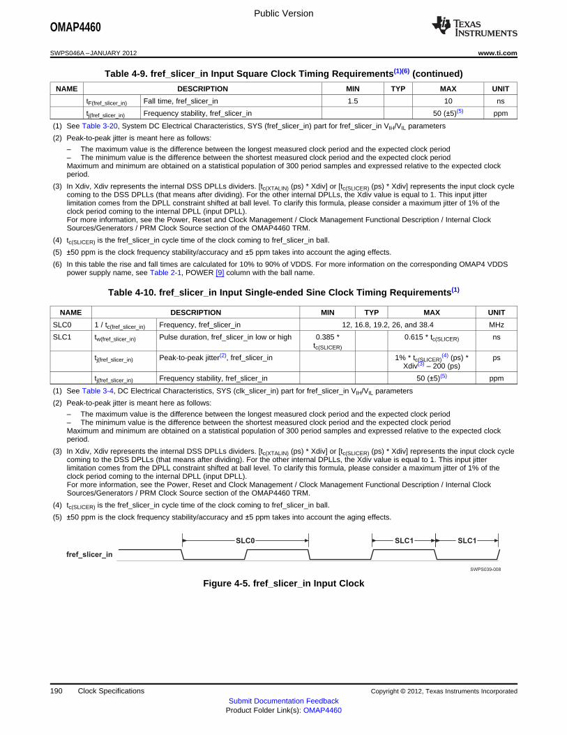
fref_slicer_in
SLC0 SLC1 SLC1
SWPS039-008
Public Version
OMAP4460
SWPS046A –JANUARY 2012 www.ti.com
Table 4-9. fref_slicer_in Input Square Clock Timing Requirements(1)(6) (continued)
NAME DESCRIPTION MIN TYP MAX UNIT
tF(fref_slicer_in) Fall time, fref_slicer_in 1.5 10 ns
tj(fref_slicer_in) Frequency stability, fref_slicer_in 50 (±5)(5) ppm
(1) See Table 3-20, System DC Electrical Characteristics, SYS (fref_slicer_in) part for fref_slicer_in VIH/VIL parameters
(2) Peak-to-peak jitter is meant here as follows:
– The maximum value is the difference between the longest measured clock period and the expected clock period– The minimum value is the difference between the shortest measured clock period and the expected clock periodMaximum and minimum are obtained on a statistical population of 300 period samples and expressed relative to the expected clockperiod.
(3) In Xdiv, Xdiv represents the internal DSS DPLLs dividers. [tc(XTALIN) (ps) * Xdiv] or [tc(SLICER) (ps) * Xdiv] represents the input clock cyclecoming to the DSS DPLLs (that means after dividing). For the other internal DPLLs, the Xdiv value is equal to 1. This input jitterlimitation comes from the DPLL constraint shifted at ball level. To clarify this formula, please consider a maximum jitter of 1% of theclock period coming to the internal DPLL (input DPLL).For more information, see the Power, Reset and Clock Management / Clock Management Functional Description / Internal ClockSources/Generators / PRM Clock Source section of the OMAP4460 TRM.
(4) tc(SLICER) is the fref_slicer_in cycle time of the clock coming to fref_slicer_in ball.
(5) ±50 ppm is the clock frequency stability/accuracy and ±5 ppm takes into account the aging effects.
(6) In this table the rise and fall times are calculated for 10% to 90% of VDDS. For more information on the corresponding OMAP4 VDDSpower supply name, see Table 2-1, POWER [9] column with the ball name.
Table 4-10. fref_slicer_in Input Single-ended Sine Clock Timing Requirements(1)
NAME DESCRIPTION MIN TYP MAX UNIT
SLC0 1 / tc(fref_slicer_in) Frequency, fref_slicer_in 12, 16.8, 19.2, 26, and 38.4 MHz
SLC1 tw(fref_slicer_in) Pulse duration, fref_slicer_in low or high 0.385 * 0.615 * tc(SLICER) nstc(SLICER)
tj(fref_slicer_in) Peak-to-peak jitter(2), fref_slicer_in 1% * tc(SLICER)(4) (ps) * ps
Xdiv(3) – 200 (ps)
tj(fref_slicer_in) Frequency stability, fref_slicer_in 50 (±5)(5) ppm
(1) See Table 3-4, DC Electrical Characteristics, SYS (clk_slicer_in) part for fref_slicer_in VIH/VIL parameters
(2) Peak-to-peak jitter is meant here as follows:
– The maximum value is the difference between the longest measured clock period and the expected clock period– The minimum value is the difference between the shortest measured clock period and the expected clock periodMaximum and minimum are obtained on a statistical population of 300 period samples and expressed relative to the expected clockperiod.
(3) In Xdiv, Xdiv represents the internal DSS DPLLs dividers. [tc(XTALIN) (ps) * Xdiv] or [tc(SLICER) (ps) * Xdiv] represents the input clock cyclecoming to the DSS DPLLs (that means after dividing). For the other internal DPLLs, the Xdiv value is equal to 1. This input jitterlimitation comes from the DPLL constraint shifted at ball level. To clarify this formula, please consider a maximum jitter of 1% of theclock period coming to the internal DPLL (input DPLL).For more information, see the Power, Reset and Clock Management / Clock Management Functional Description / Internal ClockSources/Generators / PRM Clock Source section of the OMAP4460 TRM.
(4) tc(SLICER) is the fref_slicer_in cycle time of the clock coming to fref_slicer_in ball.
(5) ±50 ppm is the clock frequency stability/accuracy and ±5 ppm takes into account the aging effects.
Figure 4-5. fref_slicer_in Input Clock
190 Clock Specifications Copyright © 2012, Texas Instruments Incorporated
Submit Documentation FeedbackProduct Folder Link(s): OMAP4460

Public Version
OMAP4460
www.ti.com SWPS046A –JANUARY 2012
4.2 Output Clocks Specifications
4.2.1 FREF Output Clocks
Each output clock source can be selected independently between the system clock (fref_xtal_in,fref_slicer_in), PER DPLL or CORE DPLL, with a programmable divider factor.
For more information, see the Power, Reset and Clock Management / PRCM Subsystem Environment /External Clock Signals section of the OMAP4460 TRM.
Table 4-11 summarizes the electrical characteristics of the fref_clk1_out output clock (specially targetedfor the primary camera sensor functional input clock), fref_clk2_out output clock (targeted for thesecondary camera sensor functional input clock), and fref_clk0_out, fref_clk3_out, fref_clk4_out,fref_clk5_out output clocks (input clocks for the other peripherals).
Table 4-11. fref_clkx_out Output Clock Electrical Characteristics(1)(3)
NAME DESCRIPTION MIN TYP MAX UNIT
f Frequency, fref_clkx_out fref_xtal_in clock frequency(2) or fref_slicer_in clock MHzfrequency(2) or PER/CORE DPLL frequency(2)
MB[0:1] = 11
LB0 = 1
CL Load capacitance (Transmission line load + Far 20 25 pFend load)
ZT Transmission line impedance 30 60 ΩLT Transmission line length NA 10 cm
DT Transmission line delay time NA 670 ps
LB0 = 0
CL Load capacitance (Transmission line load + Far 14 17 pFend load)
ZT Transmission line impedance 30 60 ΩLT Transmission line length NA 5 cm
DT Transmission line delay time NA 335 ps
MB[0:1] = 01
LB0 = 1
CL Load capacitance (Transmission line load + Far 23 28 pFend load)
ZT Transmission line impedance 30 55 ΩLT Transmission line length NA 12.5 cm
DT Transmission line delay time NA 838 ps
LB0 = 0
CL Load capacitance (Transmission line load + Far 2 11 pFend load)
ZT Transmission line impedance 30 60 ΩLT Transmission line length NA 8 cm
DT Transmission line delay time NA 536 ps
(1) In fref_clkx_out, x = 0, 1, 2, 3, 4, or 5
(2) Possible clock divisions: [1 to 16]
(3) The modes are configured by 3 bits MB[0:1] and LB0 of the IO cell. For more details, see the OMAP4460 TRM.
Table 4-12 details the fref_clk0_out, fref_clk1_out, fref_clk2_out, fref_clk3_out, fref_clk4_out, andfref_clk5_out output clock switching characteristics.
Copyright © 2012, Texas Instruments Incorporated Clock Specifications 191Submit Documentation Feedback
Product Folder Link(s): OMAP4460
Public Version
OMAP4460
SWPS046A –JANUARY 2012 www.ti.com
Table 4-12. fref_clkx_out Output Clock Switching Characteristics(1)(6)
NAME DESCRIPTION MIN TYP MAX UNIT
f Frequency, fref_clkx_out fref_xtal_in clock frequency(2) or MHzfref_slicer_in clock frequency(2) or
Per/Core DPLL frequency(2)
FREF0 tc(clkOUT1) Period, fref_clkx_out fref_xtal_in clock period or fref_slicer_in nsclock period or
Per/Core DPLL period
tJ Peak-to-peak jitter, fref_clkx_out From fref_xtal_in tJ(fref_xtal_in)(9) + ps
Core DPLL or Per 400 psDPLL bypassed
From fref_xtal_in tJ(fref_xtal_in)(9) +
Core DPLL or Per 340 psDPLL used
From tJ(fref_slicer_in)(9) +
fref_slicer_in Core 440 psDPLL or PerDPLL bypassed
From tJ(fref_slicer_in)(9) +
fref_slicer_in Core 310 psDPLL or PerDPLL used
Stability, fref_clkx_out ± 50 (± 5)(8) ppm
FREF1 tw(clkout1) Pulse duration, Divider(7) value From fref_xtal_in 0.50 * tc(clkout1) + nsfref_clkx_out is even Core DPLL or Per [tJ(fref_xtal_in)
(9) +low or high DPLL bypassed 400 ps]
From fref_xtal_in 0.50 * tc(clkout1) +Core DPLL or Per [tJ(fref_xtal_in)
(9) +DPLL used 340 ps]
From 0.50 * tc(clkout1) +fref_slicer_in Core [tJ(fref_slicer_in)
(9) +DPLL or Per 440 ps]DPLL bypassed
From 0.50 * tc(clkout1) +fref_slicer_in Core [tJ(fref_slicer_in)
(9) +DPLL or Per 310 ps]DPLL used
Divider(7) value From fref_xtal_in (divider(7) – 1) /is odd Core DPLL or Per (2*divider(7)) *
DPLL bypassed tc(clkout1) +[tJ(fref_xtal_in)
(9) +400 ps]
From fref_xtal_in (divider(7) – 1) /Core DPLL or Per (2*divider(7)) *DPLL used tc(clkout1) +
[tJ(fref_xtal_in)(9) +
340 ps]
From (divider(7) – 1) /fref_slicer_in Core (2*divider(7)) *DPLL or Per tc(clkout1) +DPLL bypassed [tJ(fref_slicer_in)
(9) +440 ps]
From (divider(7) – 1) /fref_slicer_in Core (2*divider(7)) *DPLL or Per tc(clkout1) +DPLL used [tJ(fref_slicer_in)
(9) +310 ps]
MB[0:1] = 11
LB0 = 1
tR(clkOUT1) Rise time, fref_clkx_out 2(3)(5) 10.0(4) ns
tF(clkOUT1) Fall time, fref_clkx_out 2(3)(5) 10.0(4) ns
LB0 = 0
192 Clock Specifications Copyright © 2012, Texas Instruments Incorporated
Submit Documentation FeedbackProduct Folder Link(s): OMAP4460
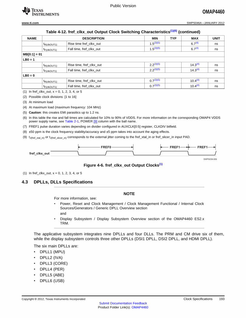
fref_clkx_out
FREF0 FREF1 FREF1
SWPS039-009
Public Version
OMAP4460
www.ti.com SWPS046A –JANUARY 2012
Table 4-12. fref_clkx_out Output Clock Switching Characteristics(1)(6) (continued)
NAME DESCRIPTION MIN TYP MAX UNIT
tR(clkOUT1) Rise time fref_clkx_out 1.5(3)(5) 6.7(4) ns
tF(clkOUT1) Fall time, fref_clkx_out 1.5(3)(5) 6.7(4) ns
MB[0:1] = 01
LB0 = 1
tR(clkOUT1) Rise time, fref_clkx_out 2.2(3)(5) 14.3(4) ns
tF(clkOUT1) Fall time, fref_clkx_out 2.2(3)(5) 14.3(4) ns
LB0 = 0
tR(clkOUT1) Rise time, fref_clkx_out 0.7(3)(5) 10.4(4) ns
tF(clkOUT1) Fall time, fref_clkx_out 0.7(3)(5) 10.4(4) ns
(1) In fref_clkx_out, x = 0, 1, 2, 3, 4, or 5
(2) Possible clock divisions: [1 to 16]
(3) At minimum load
(4) At maximum load (maximum frequency: 104 MHz)
(5) Caution: this creates EMI parasitics up to 1.2 ns.
(6) In this table the rise and fall times are calculated for 10% to 90% of VDDS. For more information on the corresponding OMAP4 VDDSpower supply name, see Table 2-1, POWER [9] column with the ball name.
(7) FREF1 pulse duration varies depending on divider configured in AUXCLK[0:5] register, CLKDIV bitfield.
(8) ±50 ppm is the clock frequency stability/accuracy and ±5 ppm takes into account the aging effects.
(9) tJ(fref_xtal_in) or tJ(fref_slicer_in) corresponds to the external jitter coming to the fref_xtal_in or fref_slicer_in input PAD.
Figure 4-6. fref_clkx_out Output Clocks(1)
(1) In fref_clkx_out, x = 0, 1, 2, 3, 4, or 5
4.3 DPLLs, DLLs Specifications
NOTEFor more information, see:
• Power, Reset and Clock Management / Clock Management Functional / Internal ClockSources/Generators / Generic DPLL Overview section
and
• Display Subsystem / Display Subsystem Overview section of the OMAP4460 ES2.xTRM.
The applicative subsystem integrates nine DPLLs and four DLLs. The PRM and CM drive six of them,while the display subsystem controls three other DPLLs (DSI1 DPLL, DSI2 DPLL, and HDMI DPLL).
The six main DPLLs are:• DPLL1 (MPU)• DPLL2 (IVA)• DPLL3 (CORE)• DPLL4 (PER)• DPLL5 (ABE)• DPLL6 (USB)
Copyright © 2012, Texas Instruments Incorporated Clock Specifications 193Submit Documentation Feedback
Product Folder Link(s): OMAP4460

Public Version
OMAP4460
SWPS046A –JANUARY 2012 www.ti.com
NOTEOf the nine DPLLs embedded in the OMAP4460 device, the DSI1 DPLL, DSI2 DPLL, andHDMI DPLL are controlled directly by the display subsystem.
4.3.1 DPLLs Characteristics
Table 4-13 and Table 4-14 summarize the DPLL characteristics and assume testing over recommendedoperating conditions.
Table 4-13. DPLL1 / DPLL2 / DPLL3 / DPLL4 / DPLL5 / DSI1 DPLL / DSI2 DPLL Characteristics
NAME DESCRIPTION MIN TYP MAX UNIT COMMENTS
vdda_dpll_iva_per Supply voltage for DPLLs (IVA 1.71 1.80 1.89 Vand PER)
vdda_dpll_mpu Supply voltage for DPLL MPU 1.71 1.80 1.89 V
vdda_dpll_core_audio Supply voltage for DPLLs (CORE 1.71 1.80 1.89 Vand AUDIO)
vdda_dsi1 Supply voltage for DSI1 DPLL 1.71 1.80 1.89 V
vdda_dsi2 Supply voltage for DSI2 DPLL 1.71 1.80 1.89 V
finput CLKINP input frequency 0.032 52 MHz FINP
fREF Internal reference clock 0.032 52 MHz REFCLKfrequency
fCLKINPHIF CLKINPHIF input frequency 10 1000 MHz FINPHIF
fCLKINPULOW CLKINPULOW input frequency 0.001 800 MHz
fCLKOUT CLKOUT output frequency 10(1) 1000(2) MHz [M / (N + 1)] * FINP *[1 / M2]
fCLKOUTx2 CLKOUTx2 output frequency 20(1) 2000(2) MHz 2 * [M / (N + 1)] *FINP * [1 / M2]
fCLKOUTHIF CLKOUTHIF output frequency 10(3) 1000(4) MHz FINPHIF / M3
20(3) 2000(4) 2 * [M / (N + 1)] *FINP * [1 / M3]
fCLKDCOLDO Digital-Controlled Oscillator 20 2000 MHz 2 * [M / (N + 1)] *(DCO) output clock frequency FINP
CLKOUT period jitter –2.5% 2.5% The period jitter at theoutput clocks isCLKOUTx2 period jitter –2.5% 2.5% ±2.5% peak to peak
CLKOUTHIF period jitter –2.5% 2.5% for REFCLK above orequal to 1 MHz. IfCLKDCOLDO period jitter –2.5% 2.5%REFCLK < 1 MHz,the output jitter is upto ±3%.
tlock Frequency lock time 1.9 + 350 * REFCLK μs
plock Phase lock time 1.9 + 500 * REFCLK μs
trelock-L Relock time—Frequency lock(5) 1.9 + 70 * REFCLK μs DPLL in low-power(Low power bypass) mode:
lowcurrstdby = 1
prelock-L Relock time—Phase lock(5) (Low 1.9 + 120 * REFCLK μs DPLL in low-powerpower bypass) mode:
lowcurrstdby = 1
trelock-F Relock time—Frequency lock(5) 0.05 + 70 * REFCLK μs DPLL in normal(Fast relock bypass) mode:
lowcurrstdby = 0
prelock-F Relock time—Phase lock(5) (Fast 0.05 + 120 * REFCLK μs DPLL in normalrelock bypass) mode:
lowcurrstdby = 0
194 Clock Specifications Copyright © 2012, Texas Instruments Incorporated
Submit Documentation FeedbackProduct Folder Link(s): OMAP4460

Public Version
OMAP4460
www.ti.com SWPS046A –JANUARY 2012
(1) The minimum frequencies on CLKOUT and CLKOUTX2 are assuming M2 = 1.For M2 > 1, the minimum frequency on these clocks will further scale down by factor of M2.
(2) The maximum frequencies on CLKOUT and CLKOUTX2 are assuming M2 = 1.
(3) The minimum frequency on CLKOUTHIF is assuming M3 = 1. For M3 > 1, the minimum frequency on this clock will further scale downby factor of M3.
(4) The maximum frequency on CLKOUTHIF is assuming M3 = 1.
(5) Relock time assumes typical operating conditions, 10°C maximum temperature drift.
Table 4-14. DPLL6/HDMI DPLL Characteristics
NAME DESCRIPTION MIN TYP MAX UNIT COMMENTS
vdda_usba0otg_1p8v Supply voltage for USB DPLL 1.71 1.80 1.89 V
vdda_hdmi_vdac Supply voltage for HDMI DPLL 1.71 1.80 1.89 V
finput Input clock frequency 0.5 60 MHz FINP
fREF Internal reference clock 0.5 2.5 MHz REFCLK = [1 / (N +frequency 1)] * FINP
fCLKINPULOW CLKINPULOW bypass input 0.001 800 MHz Bypass modeclock frequency (supported by
DPLL6):fCLKOUT = fCLKINPULOW
fCLKOUTLDO CLKOUTLDO output clock 500(1) 2000(2) MHz [M / (N + 1)] * FINP *frequency [1 / M2]
fCLKOUT CLKOUT output clock frequency 500(1) 2000(2) MHz [M / (N + 1)] * FINP *[1 / M2]
fCLKDCOLDO Digital-controlled oscillator (DCO) 500 2000 MHz [M / (N + 1)] * FINPoutput clock frequency
CLKOUT period jitter –2.5% 2.5% The period jitter at theoutput clocks isCLKDCOLDO period jitter –2.5% 2.5% ±2.5% peak to peak
tlock Frequency lock time 350 * REFCLKs µs
plock Phase lock time 500 * REFCLKs µs
trelock-L Relock time—Frequency lock(3) 7.5 + 30 * REFCLKs µs(Low power bypass)
prelock-L Relock time—Phase lock(3) (Low 7.5 + 125 * REFCLKs µspower bypass)
(1) The minimum frequency on this clock is assuming M2 = 1.For M2 > 1, the minimum frequency on this clock will further scale down to 10 MHz by factor of M2.
(2) The maximum frequency on this clock is assuming M2 = 1.
(3) Relock time assumes typical operating conditions, 10°C maximum temperature drift.
Copyright © 2012, Texas Instruments Incorporated Clock Specifications 195Submit Documentation Feedback
Product Folder Link(s): OMAP4460

Public Version
OMAP4460
SWPS046A –JANUARY 2012 www.ti.com
4.3.2 DLLs Characteristics
Table 4-15 summarizes the DLL characteristics and assumes testing over recommended operatingconditions.
Table 4-15. DLL Characteristics
NAME DESCRIPTION MIN TYP MAX UNIT
vdda_dll0_lpddr21 LPDDR21 power supply providing clocks to bytes 0 and 2 See (2) V
vdda_dll1_lpddr21 LPDDR21 power supply providing clocks to bytes 1 and 3 See (2) V
vdda_dll0_lpddr22 LPDDR22 power supply providing clocks to bytes 0 and 2 See (2) V
vdda_dll1_lpddr22 LPDDR22 power supply providing clocks to bytes 1 and 3 See (2) V
finput Input clock frequency(1) 48 400 MHz
tlock Lock time 400 cycles
trelock Relock time (a change of the DLL frequency implies that DLL 400 cyclesmust relock)
(1) Maximum frequency for minimal conditions
(2) The DLL power supplies (vdda_dll0_lpddr21, vdda_dll0_lpddr22, vdda_dll1_lpddr21, vdda_dll1_lpddr22) voltage ranges follow thevdd_core voltage ones. They can be shorted with vdd_core. See the operating condition addendum for values.
4.3.3 DPLLs and DLLs Noise Isolation
NOTEFor more information on DPLLs and DLLs decoupling capacitors requirements, seeSection 3.4.1.3, Analog Voltage Decoupling.
4.4 Internal 32-kHz Oscillator
An internal 32-kHz oscillator is implemented in the wake-up domain. Table 4-16 gives the internal 32-kHzoscillator characteristic.
Table 4-16. Internal 32-kHz Oscillator Characteristic
PARAMETER MIN TYP MAX UNIT
Internal 32-kHz oscillator frequency 16 32 60 kHz
196 Clock Specifications Copyright © 2012, Texas Instruments Incorporated
Submit Documentation FeedbackProduct Folder Link(s): OMAP4460
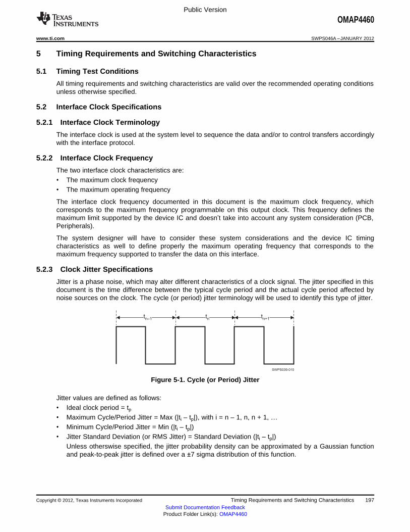
SWPS039-010
tn–1
tn
tn+1
Public Version
OMAP4460
www.ti.com SWPS046A –JANUARY 2012
5 Timing Requirements and Switching Characteristics
5.1 Timing Test Conditions
All timing requirements and switching characteristics are valid over the recommended operating conditionsunless otherwise specified.
5.2 Interface Clock Specifications
5.2.1 Interface Clock Terminology
The interface clock is used at the system level to sequence the data and/or to control transfers accordinglywith the interface protocol.
5.2.2 Interface Clock Frequency
The two interface clock characteristics are:• The maximum clock frequency• The maximum operating frequency
The interface clock frequency documented in this document is the maximum clock frequency, whichcorresponds to the maximum frequency programmable on this output clock. This frequency defines themaximum limit supported by the device IC and doesn’t take into account any system consideration (PCB,Peripherals).
The system designer will have to consider these system considerations and the device IC timingcharacteristics as well to define properly the maximum operating frequency that corresponds to themaximum frequency supported to transfer the data on this interface.
5.2.3 Clock Jitter Specifications
Jitter is a phase noise, which may alter different characteristics of a clock signal. The jitter specified in thisdocument is the time difference between the typical cycle period and the actual cycle period affected bynoise sources on the clock. The cycle (or period) jitter terminology will be used to identify this type of jitter.
Figure 5-1. Cycle (or Period) Jitter
Jitter values are defined as follows:• Ideal clock period = tp• Maximum Cycle/Period Jitter = Max (|ti – tp|), with i = n – 1, n, n + 1, …• Minimum Cycle/Period Jitter = Min (|ti – tp|)• Jitter Standard Deviation (or RMS Jitter) = Standard Deviation (|ti – tp|)
Unless otherswise specified, the jitter probability density can be approximated by a Gaussian functionand peak-to-peak jitter is defined over a ±7 sigma distribution of this function.
Copyright © 2012, Texas Instruments Incorporated Timing Requirements and Switching Characteristics 197Submit Documentation Feedback
Product Folder Link(s): OMAP4460
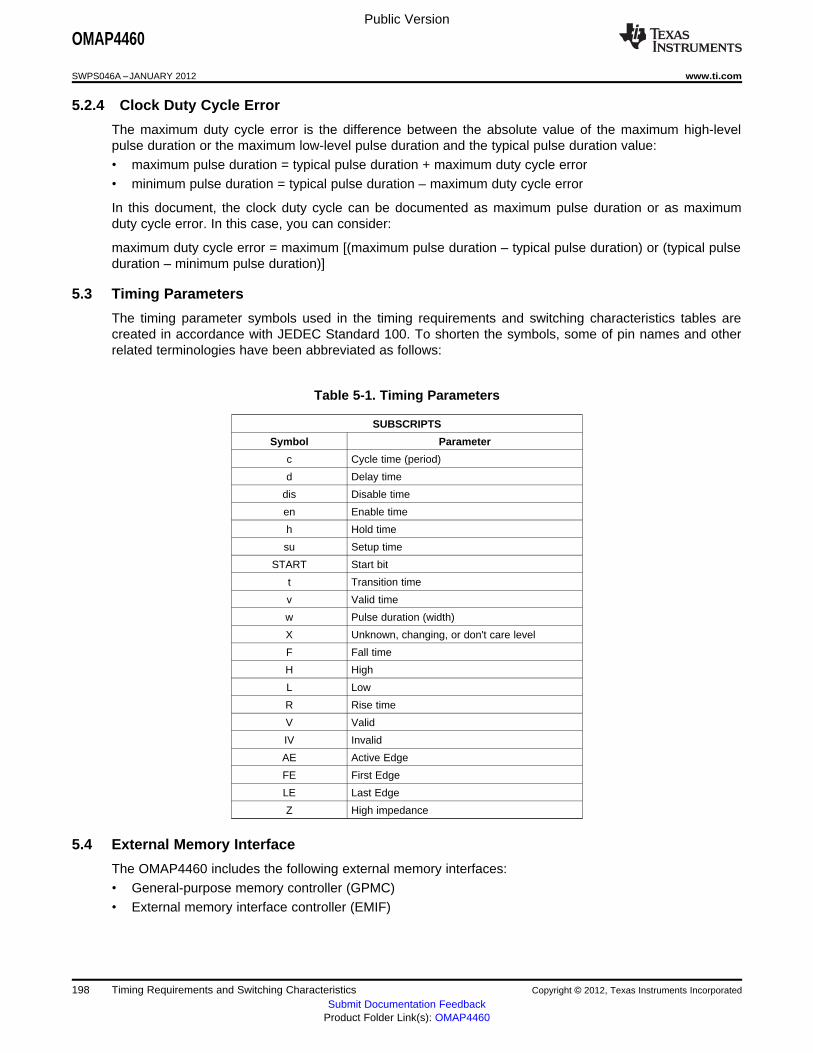
Public Version
OMAP4460
SWPS046A –JANUARY 2012 www.ti.com
5.2.4 Clock Duty Cycle Error
The maximum duty cycle error is the difference between the absolute value of the maximum high-levelpulse duration or the maximum low-level pulse duration and the typical pulse duration value:• maximum pulse duration = typical pulse duration + maximum duty cycle error• minimum pulse duration = typical pulse duration – maximum duty cycle error
In this document, the clock duty cycle can be documented as maximum pulse duration or as maximumduty cycle error. In this case, you can consider:
maximum duty cycle error = maximum [(maximum pulse duration – typical pulse duration) or (typical pulseduration – minimum pulse duration)]
5.3 Timing Parameters
The timing parameter symbols used in the timing requirements and switching characteristics tables arecreated in accordance with JEDEC Standard 100. To shorten the symbols, some of pin names and otherrelated terminologies have been abbreviated as follows:
Table 5-1. Timing Parameters
SUBSCRIPTS
Symbol Parameter
c Cycle time (period)
d Delay time
dis Disable time
en Enable time
h Hold time
su Setup time
START Start bit
t Transition time
v Valid time
w Pulse duration (width)
X Unknown, changing, or don't care level
F Fall time
H High
L Low
R Rise time
V Valid
IV Invalid
AE Active Edge
FE First Edge
LE Last Edge
Z High impedance
5.4 External Memory Interface
The OMAP4460 includes the following external memory interfaces:• General-purpose memory controller (GPMC)• External memory interface controller (EMIF)
198 Timing Requirements and Switching Characteristics Copyright © 2012, Texas Instruments Incorporated
Submit Documentation FeedbackProduct Folder Link(s): OMAP4460
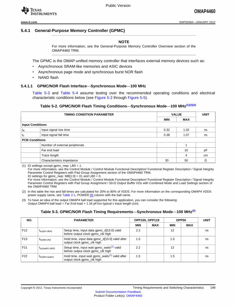
Public Version
OMAP4460
www.ti.com SWPS046A –JANUARY 2012
5.4.1 General-Purpose Memory Controller (GPMC)
NOTEFor more information, see the General-Purpose Memory Controller Overview section of theOMAP4460 TRM.
The GPMC is the OMAP-unified memory controller that interfaces external memory devices such as:• Asynchronous SRAM-like memories and ASIC devices• Asynchronous page mode and synchronous burst NOR flash• NAND flash
5.4.1.1 GPMC/NOR Flash Interface—Synchronous Mode—100 MHz
Table 5-3 and Table 5-4 assume testing over the recommended operating conditions and electricalcharacteristic conditions below (see Figure 5-2 through Figure 5-5).
Table 5-2. GPMC/NOR Flash Timing Conditions—Synchronous Mode—100 MHz(1)(2)(3)
TIMING CONDITION PARAMETER VALUE UNIT
MIN MAX
Input Conditions
tR Input signal rise time 0.32 1.02 ns
tF Input signal fall time 0.38 1.07 ns
PCB Conditions
Number of external peripherals 1
Far end load 10 pF
Trace length 4 cm
Characteristics impedance 30 50 Ω
(1) IO settings except gpmc_nwp: LB0 = 1.For more information, see the Control Module / Control Module Functional Description/ Functional Register Description / Signal IntegrityParameter Control Registers with Pad Group Assignment section of the OMAP4460 TRM.IO settings for gpmc_nwp: MB[1:0] = 01 and LB0 = 0.For more information, see the Control Module / Control Module Functional Description/ Functional Register Description / Signal IntegrityParameter Control Registers with Pad Group Assignment / 50-Ω Output Buffer I/Os with Combined Mode and Load Settings section ofthe OMAP4460 TRM.
(2) In this table the rise and fall times are calculated for 20% to 80% of VDDS. For more information on the corresponding OMAP4 VDDSpower supply name, see Table 2-1, POWER [9] column with the ball name.
(3) To have an idea of the output OMAP4 ball load supported for this application, you can consider the following:Output OMAP4 ball load = Far End load + 1.34 pF/cm typical x trace length (cm).
Table 5-3. GPMC/NOR Flash Timing Requirements—Synchronous Mode—100 MHz(2)
NO. PARAMETER OPP100, OPP119 OPP50 UNIT
MIN MAX MIN MAX
F12 tsu(dV-clkH) Setup time, input data gpmc_d[15:0] valid 2.2 12 nsbefore output clock gpmc_clk high
F13 th(clkH-dV) Hold time, input data gpmc_d[15:0] valid after 1.5 1.5 nsoutput clock gpmc_clk high
F21 tsu(waitV-clkH) Setup time, input wait gpmc_waitx(1) valid 2.2 12 nsbefore output clock gpmc_clk high
F22 th(clkH-waitV) Hold time, input wait gpmc_waitx(1) valid after 1.5 1.5 nsoutput clock gpmc_clk high
Copyright © 2012, Texas Instruments Incorporated Timing Requirements and Switching Characteristics 199Submit Documentation Feedback
Product Folder Link(s): OMAP4460

Public Version
OMAP4460
SWPS046A –JANUARY 2012 www.ti.com
(1) In gpmc_waitx, x is equal to 0, 1, 2, or 3.
(2) See DM Operating Condition Addendum for CORE OPP voltages.
Table 5-4. GPMC/NOR Flash Switching Characteristics—Synchronous Mode—100 MHz
NO. PARAMETER OPP100, OPP119 OPP50 UNIT
MIN MAX MIN MAX
F0 1 / tc(clk) Frequency(15), output clock gpmc_clk 100 50 MHz
F1 tw(clkH) Typical pulse duration, output clock 0.5 P(12) 0.5 P(12) nsgpmc_clk high
F1 tw(clkL) Typical pulse duration, output clock 0.5 P(12) 0.5 P(12) nsgpmc_clk low
tdc(clk) Duty cycle error, output clk gpmc_clk –500.00 500.00 –1000.00 1000.00 ps
tj(clk) Jitter standard deviation(16), output 64.7 64.7 psclock gpmc_clk
tR(clk) Rise time, output clock gpmc_clk 0.230 1.430 0.230 1.430 ns
tF(clk) Fall time, output clock gpmc_clk 0.227 1.550 0.227 1.550 ns
tR(DO) Rise time, output data gpmc_d[15:0] 0.230 1.430 0.230 1.430 ns
tF(DO) Fall time, output data gpmc_d[15:0] 0.227 1.550 0.227 1.550 ns
F2 td(clkH-nCSV) Delay time, gpmc_clk rising edge to F(6) – 1.9 F(6) + 3.1 F(6) – 5.1 F(6) + 8.1 nsgpmc_ncsx(11) transition
F3 td(clkH-nCSIV) Delay time, gpmc_clk rising edge to E(5) – 1.9 E(5) + 3.1 E(5) – 5.1 E(5) + 8.1 nsgpmc_ncsx(11) invalid
F4 td(ADDV-clk) Delay time, gpmc_a[26:17] / B(2) – 3.1 B(2) + 2.1 B(2) – 8.1 B(2) + 5.1 nsgpmc_a[16:1] /gpmc_a[10:1] addressbus valid to gpmc_clk first edge
F5 td(clkH-ADDIV) Delay time, gpmc_clk rising edge to –2.1 –5.1 nsgpmc_a[16:1] gpmc address businvalid
F8 td(clkH-nADV) Delay time, gpmc_clk rising edge to G(7) – 1.9 G(7) + 3.1 G(7) – 5.1 G(7) + 8.1 nsgpmc_nadv_ale transition
F9 td(clkH-nADVIV) Delay time, gpmc_clk rising edge to D(4) – 1.9 D(4) + 3.1 D(4) – 5.1 D(4) + 8.1 nsgpmc_nadv_ale invalid
F10 td(clkH-nOE) Delay time, gpmc_clk rising edge to H(8) – 2.1 H(8) + 2.1 H(8) – 5.1 H(8) + 4.1 nsgpmc_noe transition
F11 td(clkH-nOEIV) Delay time, gpcm rising edge to E(5) – 2.1 E(5) + 2.1 E(5) – 5.1 E(5) + 4.1 nsgpmc_noe invalid
F18 tw(nCSV) Pulse duration, Read A(1) A(1) nsgpmc_ncsi(11) low Write A(1) A(1) ns
F19 tw(nBEV) Pulse duration, Read C(3) C(3) nsgpmc_nbe0_cle, Write C(3) C(3) nsgpmc_nbe1 low
F20 tw(nADVV) Pulse duration, Read K(13) K(13) nsgpmc_nadv_ale low Write K(13) K(13) ns
F23 td(clkH-IODIR) Delay time, gpmc_clk rising edge to H(8) – 2.1 H(8) + 2.1 H(8) – 5.1 H(8) + 4.1 nsgpmc_io_dir high (IN direction)
F24 td(clkH-IODIRIV) Delay time, gpmc_clk rising edge to M(17) – 2.1 M(17) + 2.1 M(17) – 5.1 M(17) + 4.1 nsgpmc_io_dir low (OUT direction)
(1) For single read: A = (CSRdOffTime – CSOnTime) * (TimeParaGranularity + 1) * GPMC_FCLK periodFor burst read: A = (CSRdOffTime – CSOnTime + (n – 1) * PageBurstAccessTime) * (TimeParaGranularity + 1) * GPMC_FCLK periodwith n the page burst access number.For burst write: A = (CSWrOffTime – CSOnTime + (n – 1) * PageBurstAccessTime) * (TimeParaGranularity + 1) * GPMC_FCLK periodwith n the page burst access number.
(2) B = ClkActivationTime * GPMC_FCLK
(3) For single read: C = RdCycleTime * (TimeParaGranularity + 1) * GPMC_FCLKFor burst read: C = (RdCycleTime + (n – 1) * PageBurstAccessTime) * (TimeParaGranularity + 1) * GPMC_FCLK with n the page burstaccess number.For Burst write: C = (WrCycleTime + (n – 1) * PageBurstAccessTime) * (TimeParaGranularity + 1) * GPMC_FCLK with n the page burst
200 Timing Requirements and Switching Characteristics Copyright © 2012, Texas Instruments Incorporated
Submit Documentation FeedbackProduct Folder Link(s): OMAP4460

Public Version
OMAP4460
www.ti.com SWPS046A –JANUARY 2012
access number.
(4) For single read: D = (RdCycleTime – AccessTime) * (TimeParaGranularity + 1) * GPMC_FCLKFor burst read: D = (RdCycleTime – AccessTime) * (TimeParaGranularity + 1) * GPMC_FCLKFor burst write: D = (WrCycleTime – AccessTime) * (TimeParaGranularity + 1) * GPMC_FCLK
(5) For single read: E = (CSRdOffTime – AccessTime) * (TimeParaGranularity + 1) * GPMC_FCLKFor burst read: E = (CSRdOffTime – AccessTime) * (TimeParaGranularity + 1) * GPMC_FCLKFor burst write: E = (CSWrOffTime – AccessTime) * (TimeParaGranularity + 1) * GPMC_FCLK
(6) For nCS falling edge (CS activated):Case GpmcFCLKDivider = 0:
– F = 0.5 * CSExtraDelay * GPMC_FCLK
Case GpmcFCLKDivider = 1:– F = 0.5 * CSExtraDelay * GPMC_FCLK if (ClkActivationTime and CSOnTime are odd) or (ClkActivationTime and CSOnTime are
even)– F = (1 + 0.5 * CSExtraDelay) * GPMC_FCLK otherwiseCase GpmcFCLKDivider = 2:– F = 0.5 * CSExtraDelay * GPMC_FCLK if ((CSOnTime – ClkActivationTime) is a multiple of 3)– F = (1 + 0.5 * CSExtraDelay) * GPMC_FCLK if ((CSOnTime – ClkActivationTime – 1) is a multiple of 3)– F = (2 + 0.5 * CSExtraDelay) * GPMC_FCLK if ((CSOnTime – ClkActivationTime – 2) is a multiple of 3)
(7) For ADV falling edge (ADV activated):Case GpmcFCLKDivider = 0:
– G = 0.5 * ADVExtraDelay * GPMC_FCLK
Case GpmcFCLKDivider = 1:– G = 0.5 * ADVExtraDelay * GPMC_FCLK if (ClkActivationTime and ADVOnTime are odd) or (ClkActivationTime and ADVOnTime
are even)– G = (1 + 0.5 * ADVExtraDelay) * GPMC_FCLK otherwise
Case GpmcFCLKDivider = 2:– G = 0.5 * ADVExtraDelay * GPMC_FCLK if ((ADVOnTime – ClkActivationTime) is a multiple of 3)– G = (1 + 0.5 * ADVExtraDelay) * GPMC_FCLK if ((ADVOnTime – ClkActivationTime – 1) is a multiple of 3)– G = (2 + 0.5 * ADVExtraDelay) * GPMC_FCLK if ((ADVOnTime – ClkActivationTime – 2) is a multiple of 3)
For ADV rising edge (ADV deactivated) in Reading mode:Case GpmcFCLKDivider = 0:– G = 0.5 * ADVExtraDelay * GPMC_FCLK
Case GpmcFCLKDivider = 1:– G = 0.5 * ADVExtraDelay * GPMC_FCLK if (ClkActivationTime and ADVRdOffTime are odd) or (ClkActivationTime and
ADVRdOffTime are even)– G = (1 + 0.5 * ADVExtraDelay) * GPMC_FCLK otherwise
Case GpmcFCLKDivider = 2:– G = 0.5 * ADVExtraDelay * GPMC_FCLK if ((ADVRdOffTime – ClkActivationTime) is a multiple of 3)– G = (1 + 0.5 * ADVExtraDelay) * GPMC_FCLK if ((ADVRdOffTime – ClkActivationTime – 1) is a multiple of 3)– G = (2 + 0.5 * ADVExtraDelay) * GPMC_FCLK if ((ADVRdOffTime – ClkActivationTime – 2) is a multiple of 3)
For ADV rising edge (ADV deactivated) in Writing mode:Case GpmcFCLKDivider = 0:– G = 0.5 * ADVExtraDelay * GPMC_FCLK
Case GpmcFCLKDivider = 1:– G = 0.5 * ADVExtraDelay * GPMC_FCLK if (ClkActivationTime and ADVWrOffTime are odd) or (ClkActivationTime and
ADVWrOffTime are even)– G = (1 + 0.5 * ADVExtraDelay) * GPMC_FCLK otherwise
Case GpmcFCLKDivider = 2:– G = 0.5 * ADVExtraDelay * GPMC_FCLK if ((ADVWrOffTime – ClkActivationTime) is a multiple of 3)– G = (1 + 0.5 * ADVExtraDelay) * GPMC_FCLK if ((ADVWrOffTime – ClkActivationTime – 1) is a multiple of 3)– G = (2 + 0.5 * ADVExtraDelay) * GPMC_FCLK if ((ADVWrOffTime – ClkActivationTime – 2) is a multiple of 3)
(8) For OE falling edge (OE activated) / IO DIR rising edge (IN direction):Case GpmcFCLKDivider = 0:
– H = 0.5 * OEExtraDelay * GPMC_FCLK
Case GpmcFCLKDivider = 1:– H = 0.5 * OEExtraDelay * GPMC_FCLK if (ClkActivationTime and OEOnTime are odd) or (ClkActivationTime and OEOnTime are
even)– H = (1 + 0.5 * OEExtraDelay) * GPMC_FCLK otherwise
Case GpmcFCLKDivider = 2:
Copyright © 2012, Texas Instruments Incorporated Timing Requirements and Switching Characteristics 201Submit Documentation Feedback
Product Folder Link(s): OMAP4460

Public Version
OMAP4460
SWPS046A –JANUARY 2012 www.ti.com
– H = 0.5 * OEExtraDelay * GPMC_FCLK if ((OEOnTime – ClkActivationTime) is a multiple of 3)– H = (1 + 0.5 * OEExtraDelay) * GPMC_FCLK if ((OEOnTime – ClkActivationTime – 1) is a multiple of 3)– H = (2 + 0.5 * OEExtraDelay) * GPMC_FCLK if ((OEOnTime – ClkActivationTime – 2) is a multiple of 3)
For OE rising edge (OE deactivated):Case GpmcFCLKDivider = 0:– H = 0.5 * OEExtraDelay * GPMC_FCLK
Case GpmcFCLKDivider = 1:– H = 0.5 * OEExtraDelay * GPMC_FCLK if (ClkActivationTime and OEOffTime are odd) or (ClkActivationTime and OEOffTime are
even)– H = (1 + 0.5 * OEExtraDelay) * GPMC_FCLK otherwise
Case GpmcFCLKDivider = 2:– H = 0.5 * OEExtraDelay * GPMC_FCLK if ((OEOffTime – ClkActivationTime) is a multiple of 3)– H = (1 + 0.5 * OEExtraDelay) * GPMC_FCLK if ((OEOffTime – ClkActivationTime – 1) is a multiple of 3)– H = (2 + 0.5 * OEExtraDelay) * GPMC_FCLK if ((OEOffTime – ClkActivationTime – 2) is a multiple of 3)
(9) For WE falling edge (WE activated):Case GpmcFCLKDivider = 0:
– I = 0.5 * WEExtraDelay * GPMC_FCLK
Case GpmcFCLKDivider = 1:– I = 0.5 * WEExtraDelay * GPMC_FCLK if (ClkActivationTime and WEOnTime are odd) or (ClkActivationTime and WEOnTime are
even)– I = (1 + 0.5 * WEExtraDelay) * GPMC_FCLK otherwise
Case GpmcFCLKDivider = 2:– I = 0.5 * WEExtraDelay * GPMC_FCLK if ((WEOnTime – ClkActivationTime) is a multiple of 3)– I = (1 + 0.5 * WEExtraDelay) * GPMC_FCLK if ((WEOnTime – ClkActivationTime – 1) is a multiple of 3)– I = (2 + 0.5 * WEExtraDelay) * GPMC_FCLK if ((WEOnTime – ClkActivationTime – 2) is a multiple of 3)
For WE rising edge (WE deactivated):Case GpmcFCLKDivider = 0:– I = 0.5 * WEExtraDelay * GPMC_FCLK
Case GpmcFCLKDivider = 1:– I = 0.5 * WEExtraDelay * GPMC_FCLK if (ClkActivationTime and WEOffTime are odd) or (ClkActivationTime and WEOffTime are
even)– I = (1 + 0.5 * WEExtraDelay) * GPMC_FCLK otherwise
Case GpmcFCLKDivider = 2:– I = 0.5 * WEExtraDelay * GPMC_FCLK if ((WEOffTime – ClkActivationTime) is a multiple of 3)– I = (1 + 0.5 * WEExtraDelay) * GPMC_FCLK if ((WEOffTime – ClkActivationTime – 1) is a multiple of 3)– I = (2 + 0.5 * WEExtraDelay) * GPMC_FCLK if ((WEOffTime – ClkActivationTime – 2) is a multiple of 3)
(10) J = GPMC_FCLK period
(11) In gpmc_ncsx, x is equal to 0, 1, 2, 3, 4, 5, 6, or 7.In gpmc_waitx, x is equal to 0, 1, 2, or 3
(12) P = gpmc_clk period
(13) For read: K = (ADVRdOffTime – ADVOnTime) * (TimeParaGranularity + 1) * GPMC_FCLKFor write: K = (ADVWrOffTime – ADVOnTime) * (TimeParaGranularity + 1) * GPMC_FCLK
(14) GPMC_FCLK is general-purpose memory controller internal functional clock
(15) Related to the gpmc_clk output clock maximum and minimum frequency programmable in I/F module by setting theGPMC_CONFIG1_CSx configuration register bit fields GpmcFCLKDivider.
(16) The jitter probability density can be approximated by a Gaussian function
(17) M = (RdCycleTime – AccessTime) * (TimeParaGranularity + 1) * GPMC_FCLKAbove M parameter expression is given as one example of GPMC programming. IO DIR signal will go from IN to OUT after bothRdCycleTime and BusTurnAround completion. Behaviour of IO direction signal does depend on kind of successive read/write accessesperformed to memory and multiplexed or nonmultiplexed memory addressing scheme, bus keeping feature enabled or not. IO DIRbehaviour is automactically handled by GPMC controller.
202 Timing Requirements and Switching Characteristics Copyright © 2012, Texas Instruments Incorporated
Submit Documentation FeedbackProduct Folder Link(s): OMAP4460
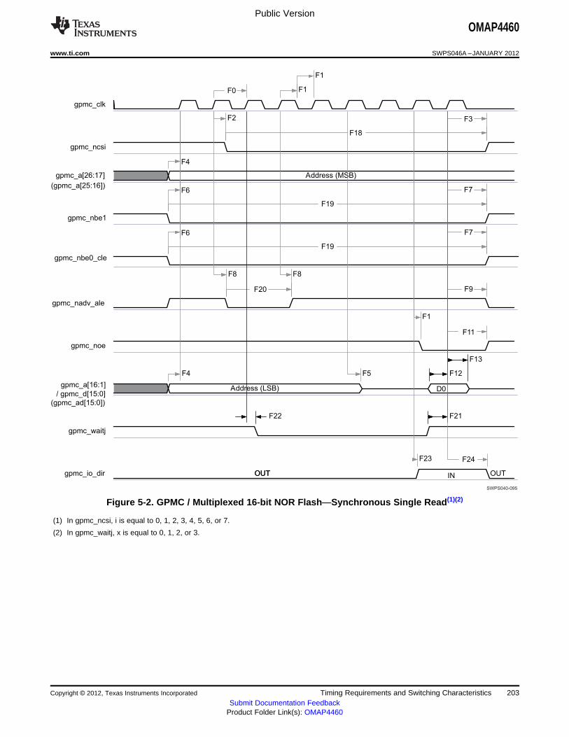
gpmc_clk
gpmc_ncsi
gpmc_a[26:17]
gpmc_nbe1
gpmc_nbe0_cle
gpmc_nadv_ale
gpmc_noe
gpmc_a[16:1]
/ gpmc_d[15:0]
gpmc_waitj
gpmc_io_dir
Address (MSB)
Address (LSB) D0
OUTOUT IN OUT
F0
F12
F13
F6
F2
F8
F3
F7
F9
F11
F1
F1
F8
F19
F18
F20
F1
F4 F5
F6 F7
F19
F4
F22 F21
F23 F24
SWPS040-095
(gpmc_a[25:16])
(gpmc_ad[15:0])
Public Version
OMAP4460
www.ti.com SWPS046A –JANUARY 2012
Figure 5-2. GPMC / Multiplexed 16-bit NOR Flash—Synchronous Single Read(1)(2)
(1) In gpmc_ncsi, i is equal to 0, 1, 2, 3, 4, 5, 6, or 7.
(2) In gpmc_waitj, x is equal to 0, 1, 2, or 3.
Copyright © 2012, Texas Instruments Incorporated Timing Requirements and Switching Characteristics 203Submit Documentation Feedback
Product Folder Link(s): OMAP4460
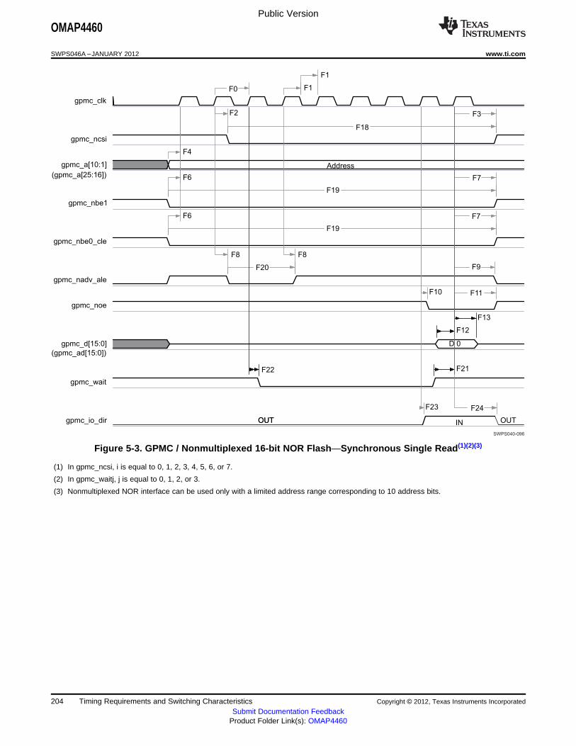
gpmc_clk
gpmc_ncsi
gpmc_a[10:1]
gpmc_nbe1
gpmc_nbe0_cle
gpmc_nadv_ale
gpmc_noe
gpmc_d[15:0]
gpmc_wait
gpmc_io_dir
Address
D 0
OUTOUT IN OUT
F0
F12
F13
F6
F2
F8
F3
F7
F9
F11
F1
F1
F8
F19
F18
F20
F10
F6 F7
F19
F4
F22 F21
F23 F24
SWPS040-096
(gpmc_a[25:16])
(gpmc_ad[15:0])
Public Version
OMAP4460
SWPS046A –JANUARY 2012 www.ti.com
Figure 5-3. GPMC / Nonmultiplexed 16-bit NOR Flash—Synchronous Single Read(1)(2)(3)
(1) In gpmc_ncsi, i is equal to 0, 1, 2, 3, 4, 5, 6, or 7.
(2) In gpmc_waitj, j is equal to 0, 1, 2, or 3.
(3) Nonmultiplexed NOR interface can be used only with a limited address range corresponding to 10 address bits.
204 Timing Requirements and Switching Characteristics Copyright © 2012, Texas Instruments Incorporated
Submit Documentation FeedbackProduct Folder Link(s): OMAP4460
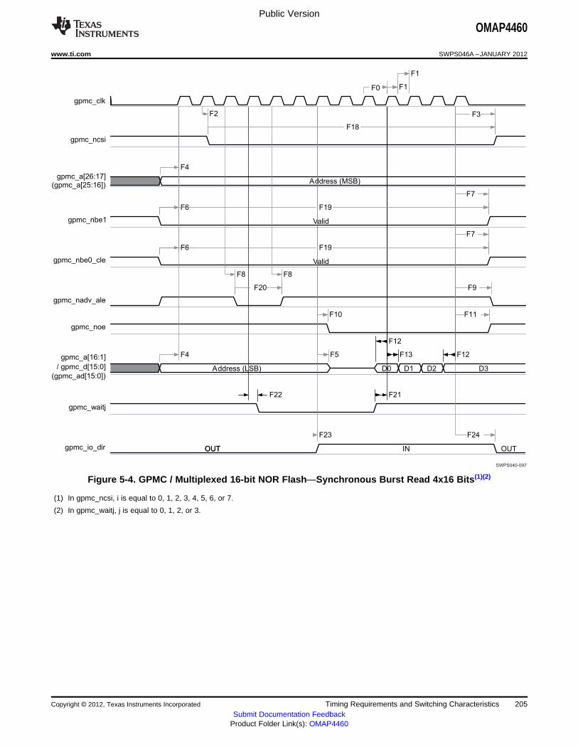
gpmc_clk
gpmc_ncsi
gpmc_a[26:17]
gpmc_nbe1
gpmc_nbe0_cle
gpmc_nadv_ale
gpmc_noe
gpmc_a[16:1]
/ gpmc_d[15:0]
gpmc_waitj
gpmc_io_dir
Address (MSB)
Valid
Valid
Address (LSB) D0 D1 D2 D3
OUTOUT IN OUT
F6
F4
F2
F8 F8
F10
F13
F12
F12
F11
F9
F7
F3
F0 F1
F1
F5
F6
F7
F22 F21
F4
F18
F20
F19
F19
F23 F24
SWPS040-097
(gpmc_a[25:16])
(gpmc_ad[15:0])
Public Version
OMAP4460
www.ti.com SWPS046A –JANUARY 2012
Figure 5-4. GPMC / Multiplexed 16-bit NOR Flash—Synchronous Burst Read 4x16 Bits(1)(2)
(1) In gpmc_ncsi, i is equal to 0, 1, 2, 3, 4, 5, 6, or 7.
(2) In gpmc_waitj, j is equal to 0, 1, 2, or 3.
Copyright © 2012, Texas Instruments Incorporated Timing Requirements and Switching Characteristics 205Submit Documentation Feedback
Product Folder Link(s): OMAP4460

gpmc_clk
gpmc_ncsi
gpmc_a[10:1]
gpmc_nbe1
gpmc_nbe0_cle
gpmc_nadv_ale
gpmc_noe
gpmc_d[15:0]
gpmc_waitj
Address
Valid
Valid
D0 D1 D2 D3
OUTOUT IN OUT
F6
F2
F8 F8
F10
F13
F12
F12
F11
F9
F7
F3
F0 F1
F1
F6
F7
F22 F21
F4
F18
F20
F19
F19
F23 F24
SWPS040-004
(gpmc_ad[15:0])
(gpmc_a[25:16])
gpmc_io_dir
Public Version
OMAP4460
SWPS046A –JANUARY 2012 www.ti.com
Figure 5-5. GPMC / Nonmultiplexed 16-bit NOR Flash—Synchronous Burst Read 4x16 Bits(1)(2)(3)
(1) In gpmc_ncsi, i is equal to 0, 1, 2, 3, 4, 5, 6, or 7.
(2) In gpmc_waitj, j is equal to 0, 1, 2, or 3.
(3) Nonmultiplexed NOR interface can be used only with a limited address range corresponding to 10 address bits.
5.4.1.2 GPMC/NOR Flash Interface—Synchronous Mode—66 MHz
Table 5-6 and Table 5-7 assume testing over the recommended operating conditions and electricalcharacteristic conditions below (see Figure 5-6 through Figure 5-11).
Table 5-5. GPMC/NOR Flash Timing Conditions—Synchronous Mode—66 MHz(1)(2)(3)
TIMING CONDITION PARAMETER VALUE UNIT
MIN MAX
Input Conditions
tR Input signal rise time 1.38 2.79 ns
tF Input signal fall time 1.14 2.85 ns
PCB Conditions
Number of external peripherals 4
Far end load 15 pF
206 Timing Requirements and Switching Characteristics Copyright © 2012, Texas Instruments Incorporated
Submit Documentation FeedbackProduct Folder Link(s): OMAP4460
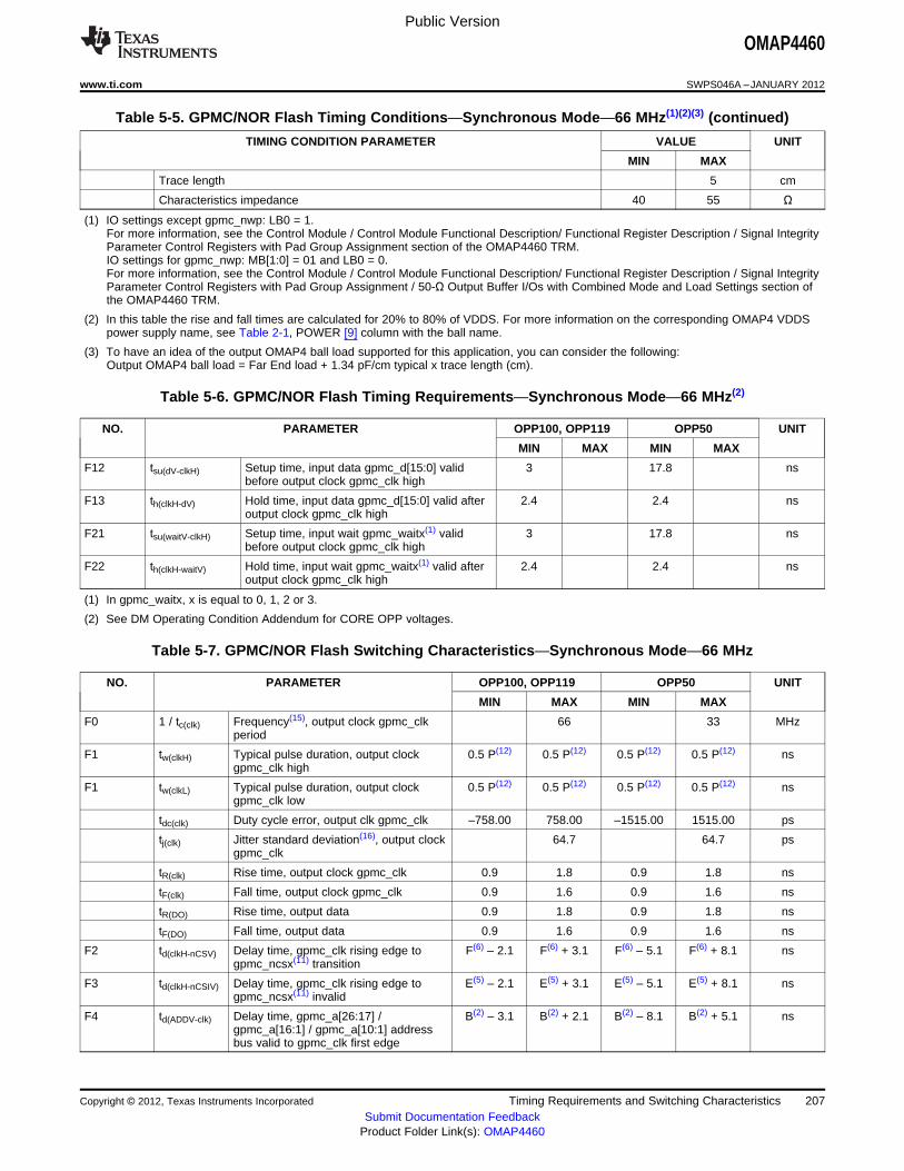
Public Version
OMAP4460
www.ti.com SWPS046A –JANUARY 2012
Table 5-5. GPMC/NOR Flash Timing Conditions—Synchronous Mode—66 MHz(1)(2)(3) (continued)
TIMING CONDITION PARAMETER VALUE UNIT
MIN MAX
Trace length 5 cm
Characteristics impedance 40 55 Ω
(1) IO settings except gpmc_nwp: LB0 = 1.For more information, see the Control Module / Control Module Functional Description/ Functional Register Description / Signal IntegrityParameter Control Registers with Pad Group Assignment section of the OMAP4460 TRM.IO settings for gpmc_nwp: MB[1:0] = 01 and LB0 = 0.For more information, see the Control Module / Control Module Functional Description/ Functional Register Description / Signal IntegrityParameter Control Registers with Pad Group Assignment / 50-Ω Output Buffer I/Os with Combined Mode and Load Settings section ofthe OMAP4460 TRM.
(2) In this table the rise and fall times are calculated for 20% to 80% of VDDS. For more information on the corresponding OMAP4 VDDSpower supply name, see Table 2-1, POWER [9] column with the ball name.
(3) To have an idea of the output OMAP4 ball load supported for this application, you can consider the following:Output OMAP4 ball load = Far End load + 1.34 pF/cm typical x trace length (cm).
Table 5-6. GPMC/NOR Flash Timing Requirements—Synchronous Mode—66 MHz(2)
NO. PARAMETER OPP100, OPP119 OPP50 UNIT
MIN MAX MIN MAX
F12 tsu(dV-clkH) Setup time, input data gpmc_d[15:0] valid 3 17.8 nsbefore output clock gpmc_clk high
F13 th(clkH-dV) Hold time, input data gpmc_d[15:0] valid after 2.4 2.4 nsoutput clock gpmc_clk high
F21 tsu(waitV-clkH) Setup time, input wait gpmc_waitx(1) valid 3 17.8 nsbefore output clock gpmc_clk high
F22 th(clkH-waitV) Hold time, input wait gpmc_waitx(1) valid after 2.4 2.4 nsoutput clock gpmc_clk high
(1) In gpmc_waitx, x is equal to 0, 1, 2 or 3.
(2) See DM Operating Condition Addendum for CORE OPP voltages.
Table 5-7. GPMC/NOR Flash Switching Characteristics—Synchronous Mode—66 MHz
NO. PARAMETER OPP100, OPP119 OPP50 UNIT
MIN MAX MIN MAX
F0 1 / tc(clk) Frequency(15), output clock gpmc_clk 66 33 MHzperiod
F1 tw(clkH) Typical pulse duration, output clock 0.5 P(12) 0.5 P(12) 0.5 P(12) 0.5 P(12) nsgpmc_clk high
F1 tw(clkL) Typical pulse duration, output clock 0.5 P(12) 0.5 P(12) 0.5 P(12) 0.5 P(12) nsgpmc_clk low
tdc(clk) Duty cycle error, output clk gpmc_clk –758.00 758.00 –1515.00 1515.00 ps
tj(clk) Jitter standard deviation(16), output clock 64.7 64.7 psgpmc_clk
tR(clk) Rise time, output clock gpmc_clk 0.9 1.8 0.9 1.8 ns
tF(clk) Fall time, output clock gpmc_clk 0.9 1.6 0.9 1.6 ns
tR(DO) Rise time, output data 0.9 1.8 0.9 1.8 ns
tF(DO) Fall time, output data 0.9 1.6 0.9 1.6 ns
F2 td(clkH-nCSV) Delay time, gpmc_clk rising edge to F(6) – 2.1 F(6) + 3.1 F(6) – 5.1 F(6) + 8.1 nsgpmc_ncsx(11) transition
F3 td(clkH-nCSIV) Delay time, gpmc_clk rising edge to E(5) – 2.1 E(5) + 3.1 E(5) – 5.1 E(5) + 8.1 nsgpmc_ncsx(11) invalid
F4 td(ADDV-clk) Delay time, gpmc_a[26:17] / B(2) – 3.1 B(2) + 2.1 B(2) – 8.1 B(2) + 5.1 nsgpmc_a[16:1] / gpmc_a[10:1] addressbus valid to gpmc_clk first edge
Copyright © 2012, Texas Instruments Incorporated Timing Requirements and Switching Characteristics 207Submit Documentation Feedback
Product Folder Link(s): OMAP4460

Public Version
OMAP4460
SWPS046A –JANUARY 2012 www.ti.com
Table 5-7. GPMC/NOR Flash Switching Characteristics—Synchronous Mode—66 MHz (continued)
NO. PARAMETER OPP100, OPP119 OPP50 UNIT
MIN MAX MIN MAX
F5 td(clkH-ADDIV) Delay time, gpmc_clk rising edge to –2.1 –5.1 nsgpmc_a[26:17] / gpmc_a[16:1] gpmcaddress bus invalid
F6 td(nBEV-clk) Delay time, gpmc_nbe0_cle, B(2) – 0.9 B(2) + 3.9 B(2) – 7.4 B(2) + 10.4 nsgpmc_nbe1 valid to gpmc_clk first edge
F7 td(clkH-nBEIV) Delay time, gpmc_clk rising edge to D(4) – 3.9 D(4) + 0.9 D(4) – 10.4 D(4) + 7.4 nsgpmc_nbe0_cle, gpmc_nbe1 invalid
F8 td(clkH-nADV) Delay time, gpmc_clk rising edge to G(7) – 1.9 G(7) + 3.1 G(7) – 4.9 G(7) + 8.1 nsgpmc_nadv_ale transition
F9 td(clkH- Delay time, gpmc_clk rising edge to D(4) – 1.9 D(4) + 3.1 D(4) – 4.9 D(4) + 8.1 nsnADVIV) gpmc_nadv_ale invalid
F10 td(clkH-nOE) Delay time, gpmc_clk rising edge to H(8) – 2.1 H(8) + 2.1 H(8) – 5.1 H(8) + 4.1 nsgpmc_noe transition
F11 td(clkH-nOEIV) Delay time, gpcm rising edge to E(5) – 2.1 E(5) + 2.1 E(5) – 5.1 E(5) + 4.1 nsgpmc_noe invalid
F14 td(clkH-nWE) Delay time, gpmc_clk rising edge to I(9) – 1.9 I(9) + 3.1 I(9) – 4.9 I(9) + 8.1 nsgpmc_nwe transition
F15 td(clkH-Data) Delay time, gpmc_clk rising edge to J(10) – 3.9 J(10) + 0.9 J(10) – 10.4 J(10) + 7.4 nsgpmc_a[26:17] / gpmc_a[16:1] data bustransition
F17 td(clkH-nBE) Delay time, gpmc_clk rising edge to J(10) – 3.9 J(10) + 0.9 J(10) – 10.4 J(10) + 7.4 nsgpmc_nbe0_cle, gpmc_nbe1 transition
F18 tw(nCSV) Pulse duration, Read A(1) A(1) nsgpmc_ncsi(11) low Write A(1) A(1) ns
F19 tw(nBEV) Pulse duration, Read C(3) C(3) nsgpmc_nbe0_cle, Write C(3) C(3) nsgpmc_nbe1 low
F20 tw(nADVV) Pulse duration, Read K(13) K(13) nsgpmc_nadv_ale low Write K(13) K(13) ns
F23 td(clkH-IODIR) Delay time, gpmc_clk rising edge to H(8) – 2.1 H(8) + 2.1 H(8) – 5.1 H(8) + 4.1 nsgpmc_io_dir high (IN direction)
F24 td(clkH- Delay time, gpcm rising edge to M(17) – 2.1 M(17) + 2.1 M(17) – 5.1 M(17) + 4.1 nsIODIRIV) gpmc_io_dir low (OUT direction)
(1) For single read:
– A = (CSRdOffTime – CSOnTime) * (TimeParaGranularity + 1) * GPMC_FCLK period
For burst read:– A = (CSRdOffTime – CSOnTime + (n – 1) * PageBurstAccessTime) * (TimeParaGranularity + 1) * GPMC_FCLK period with n the
page burst access number.
For burst write:– A = (CSWrOffTime – CSOnTime + (n – 1) * PageBurstAccessTime) * (TimeParaGranularity + 1) * GPMC_FCLK period with n the
page burst access number.
(2) B = ClkActivationTime * GPMC_FCLK
(3) For single read:
– C = RdCycleTime * (TimeParaGranularity + 1) * GPMC_FCLK
For burst read:– C = (RdCycleTime + (n – 1) * PageBurstAccessTime) * (TimeParaGranularity + 1) * GPMC_FCLK with n the page burst access
number.
For burst write:– C = (WrCycleTime + (n – 1) * PageBurstAccessTime) * (TimeParaGranularity + 1) * GPMC_FCLK with n the page burst access
number.
(4) For single read:
– D = (RdCycleTime – AccessTime) * (TimeParaGranularity + 1) * GPMC_FCLK
For burst read:
208 Timing Requirements and Switching Characteristics Copyright © 2012, Texas Instruments Incorporated
Submit Documentation FeedbackProduct Folder Link(s): OMAP4460
Public Version
OMAP4460
www.ti.com SWPS046A –JANUARY 2012
– D = (RdCycleTime – AccessTime) * (TimeParaGranularity + 1) * GPMC_FCLK
For burst write:– D = (WrCycleTime – AccessTime) * (TimeParaGranularity + 1) * GPMC_FCLK
(5) For single read:
– E = (CSRdOffTime – AccessTime) * (TimeParaGranularity + 1) * GPMC_FCLK
For burst read:– E = (CSRdOffTime – AccessTime) * (TimeParaGranularity + 1) * GPMC_FCLK
For burst write:– E = (CSWrOffTime – AccessTime) * (TimeParaGranularity + 1) * GPMC_FCLK
(6) For nCS falling edge (CS activated):Case GpmcFCLKDivider = 0:
– F = 0.5 * CSExtraDelay * GPMC_FCLK
Case GpmcFCLKDivider = 1:– F = 0.5 * CSExtraDelay * GPMC_FCLK if (ClkActivationTime and CSOnTime are odd) or (ClkActivationTime and CSOnTime are
even)– F = (1 + 0.5 * CSExtraDelay) * GPMC_FCLK otherwise
Case GpmcFCLKDivider = 2:– F = 0.5 * CSExtraDelay * GPMC_FCLK if ((CSOnTime – ClkActivationTime) is a multiple of 3)– F = (1 + 0.5 * CSExtraDelay) * GPMC_FCLK if ((CSOnTime – ClkActivationTime – 1) is a multiple of 3)– F = (2 + 0.5 * CSExtraDelay) * GPMC_FCLK if ((CSOnTime – ClkActivationTime – 2) is a multiple of 3)
(7) For ADV falling edge (ADV activated):Case GpmcFCLKDivider = 0:
– G = 0.5 * ADVExtraDelay * GPMC_FCLK
Case GpmcFCLKDivider = 1:– G = 0.5 * ADVExtraDelay * GPMC_FCLK if (ClkActivationTime and ADVOnTime are odd) or (ClkActivationTime and ADVOnTime
are even)– G = (1 + 0.5 * ADVExtraDelay) * GPMC_FCLK otherwise
Case GpmcFCLKDivider = 2:– G = 0.5 * ADVExtraDelay * GPMC_FCLK if ((ADVOnTime – ClkActivationTime) is a multiple of 3)– G = (1 + 0.5 * ADVExtraDelay) * GPMC_FCLK if ((ADVOnTime – ClkActivationTime – 1) is a multiple of 3)– G = (2 + 0.5 * ADVExtraDelay) * GPMC_FCLK if ((ADVOnTime – ClkActivationTime – 2) is a multiple of 3)
For ADV rising edge (ADV deactivated) in Reading mode:Case GpmcFCLKDivider = 0:– G = 0.5 * ADVExtraDelay * GPMC_FCLK
Case GpmcFCLKDivider = 1:– G = 0.5 * ADVExtraDelay * GPMC_FCLK if (ClkActivationTime and ADVRdOffTime are odd) or (ClkActivationTime and
ADVRdOffTime are even)– G = (1 + 0.5 * ADVExtraDelay) * GPMC_FCLK otherwise
Case GpmcFCLKDivider = 2:– G = 0.5 * ADVExtraDelay * GPMC_FCLK if ((ADVRdOffTime – ClkActivationTime) is a multiple of 3)– G = (1 + 0.5 * ADVExtraDelay) * GPMC_FCLK if ((ADVRdOffTime – ClkActivationTime – 1) is a multiple of 3)– G = (2 + 0.5 * ADVExtraDelay) * GPMC_FCLK if ((ADVRdOffTime – ClkActivationTime – 2) is a multiple of 3)
For ADV rising edge (ADV deactivated) in Writing mode:Case GpmcFCLKDivider = 0:– G = 0.5 * ADVExtraDelay * GPMC_FCLK
Case GpmcFCLKDivider = 1:– G = 0.5 * ADVExtraDelay * GPMC_FCLK if (ClkActivationTime and ADVWrOffTime are odd) or (ClkActivationTime and
ADVWrOffTime are even)– G = (1 + 0.5 * ADVExtraDelay) * GPMC_FCLK otherwise
Case GpmcFCLKDivider = 2:– G = 0.5 * ADVExtraDelay * GPMC_FCLK if ((ADVWrOffTime – ClkActivationTime) is a multiple of 3)– G = (1 + 0.5 * ADVExtraDelay) * GPMC_FCLK if ((ADVWrOffTime – ClkActivationTime – 1) is a multiple of 3)– G = (2 + 0.5 * ADVExtraDelay) * GPMC_FCLK if ((ADVWrOffTime – ClkActivationTime – 2) is a multiple of 3)
(8) For OE falling edge (OE activated) / IO DIR rising edge (IN direction):Case GpmcFCLKDivider = 0:
– H = 0.5 * OEExtraDelay * GPMC_FCLK
Copyright © 2012, Texas Instruments Incorporated Timing Requirements and Switching Characteristics 209Submit Documentation Feedback
Product Folder Link(s): OMAP4460

Public Version
OMAP4460
SWPS046A –JANUARY 2012 www.ti.com
Case GpmcFCLKDivider = 1:– H = 0.5 * OEExtraDelay * GPMC_FCLK if (ClkActivationTime and OEOnTime are odd) or (ClkActivationTime and OEOnTime are
even)– H = (1 + 0.5 * OEExtraDelay) * GPMC_FCLK otherwise
Case GpmcFCLKDivider = 2:– H = 0.5 * OEExtraDelay * GPMC_FCLK if ((OEOnTime – ClkActivationTime) is a multiple of 3)– H = (1 + 0.5 * OEExtraDelay) * GPMC_FCLK if ((OEOnTime – ClkActivationTime – 1) is a multiple of 3)– H = (2 + 0.5 * OEExtraDelay) * GPMC_FCLK if ((OEOnTime – ClkActivationTime – 2) is a multiple of 3)
For OE rising edge (OE deactivated):Case GpmcFCLKDivider = 0:– H = 0.5 * OEExtraDelay * GPMC_FCLK
Case GpmcFCLKDivider = 1:– H = 0.5 * OEExtraDelay * GPMC_FCLK if (ClkActivationTime and OEOffTime are odd) or (ClkActivationTime and OEOffTime are
even)– H = (1 + 0.5 * OEExtraDelay) * GPMC_FCLK otherwise
Case GpmcFCLKDivider = 2:– H = 0.5 * OEExtraDelay * GPMC_FCLK if ((OEOffTime – ClkActivationTime) is a multiple of 3)– H = (1 + 0.5 * OEExtraDelay) * GPMC_FCLK if ((OEOffTime – ClkActivationTime – 1) is a multiple of 3)– H = (2 + 0.5 * OEExtraDelay) * GPMC_FCLK if ((OEOffTime – ClkActivationTime – 2) is a multiple of 3)
(9) For WE falling edge (WE activated):Case GpmcFCLKDivider = 0:
– I = 0.5 * WEExtraDelay * GPMC_FCLK
Case GpmcFCLKDivider = 1:– I = 0.5 * WEExtraDelay * GPMC_FCLK if (ClkActivationTime and WEOnTime are odd) or (ClkActivationTime and WEOnTime are
even)– I = (1 + 0.5 * WEExtraDelay) * GPMC_FCLK otherwise
Case GpmcFCLKDivider = 2:– I = 0.5 * WEExtraDelay * GPMC_FCLK if ((WEOnTime – ClkActivationTime) is a multiple of 3)– I = (1 + 0.5 * WEExtraDelay) * GPMC_FCLK if ((WEOnTime – ClkActivationTime – 1) is a multiple of 3)– I = (2 + 0.5 * WEExtraDelay) * GPMC_FCLK if ((WEOnTime – ClkActivationTime – 2) is a multiple of 3)
For WE rising edge (WE deactivated):Case GpmcFCLKDivider = 0:– I = 0.5 * WEExtraDelay * GPMC_FCLK
Case GpmcFCLKDivider = 1:– I = 0.5 * WEExtraDelay * GPMC_FCLK if (ClkActivationTime and WEOffTime are odd) or (ClkActivationTime and WEOffTime are
even)– I = (1 + 0.5 * WEExtraDelay) * GPMC_FCLK otherwise
Case GpmcFCLKDivider = 2:– I = 0.5 * WEExtraDelay * GPMC_FCLK if ((WEOffTime – ClkActivationTime) is a multiple of 3)– I = (1 + 0.5 * WEExtraDelay) * GPMC_FCLK if ((WEOffTime – ClkActivationTime – 1) is a multiple of 3)– I = (2 + 0.5 * WEExtraDelay) * GPMC_FCLK if ((WEOffTime – ClkActivationTime – 2) is a multiple of 3)
(10) J = GPMC_FCLK period
(11) In gpmc_ncsx, x is equal to 0, 1, 2, 3, 4, 5, 6, or 7.In gpmc_waitx, x is equal to 0, 1, 2, or 3.
(12) P = gpmc_clk period
(13) For read: K = (ADVRdOffTime – ADVOnTime) * (TimeParaGranularity + 1) * GPMC_FCLKFor write: K = (ADVWrOffTime – ADVOnTime) * (TimeParaGranularity + 1) * GPMC_FCLK
(14) GPMC_FCLK is General Purpose Memory Controller internal functional clock.
(15) Related to the gpmc_clk output clock maximum and minimum frequency programmable in I/F module by setting theGPMC_CONFIG1_CSx configuration register bit fields GpmcFCLKDivider
(16) The jitter probability density can be approximated by a Gaussian function.
(17) M = (RdCycleTime – AccessTime) * (TimeParaGranularity + 1) * GPMC_FCLKAbove M parameter expression is given as one example of GPMC programming. IO DIR signal will go from IN to OUT after bothRdCycleTime and BusTurnAround completion. Behaviour of IO direction signal does depend on kind of successive Read/Write accessesperformed to Memory and multiplexed or nonmultiplexed memory addressing scheme, bus keeping feature enabled or not. IO DIRbehaviour is automactically handled by GPMC controller.
210 Timing Requirements and Switching Characteristics Copyright © 2012, Texas Instruments Incorporated
Submit Documentation FeedbackProduct Folder Link(s): OMAP4460
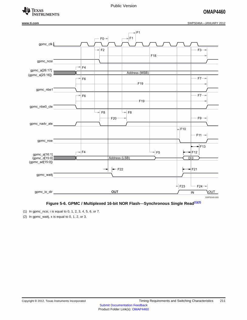
gpmc_clk
gpmc_ncsi
gpmc_a[26:17]
gpmc_nbe1
gpmc_nbe0_cle
gpmc_nadv_ale
gpmc_noe
gpmc_a[16:1]/gpmc_d[15:0]
gpmc_waitj
gpmc_io_dir
Address (MSB)
Address (LSB) D 0
OUTOUT IN OUT
F0
F12
F13
F6
F2
F8
F3
F7
F9
F11
F1
F1
F8
F19
F18
F20
F10
F4 F5
F6 F7
F19
F4
F22 F21
F23 F24
SWPS040-005
(gpmc_a[25:16])
(gpmc_ad[15:0])
Public Version
OMAP4460
www.ti.com SWPS046A –JANUARY 2012
Figure 5-6. GPMC / Multiplexed 16-bit NOR Flash—Synchronous Single Read(1)(2)
(1) In gpmc_ncsi, i is equal to 0, 1, 2, 3, 4, 5, 6, or 7.
(2) In gpmc_waitj, x is equal to 0, 1, 2, or 3.
Copyright © 2012, Texas Instruments Incorporated Timing Requirements and Switching Characteristics 211Submit Documentation Feedback
Product Folder Link(s): OMAP4460

gpmc_clk
gpmc_ncsi
gpmc_a[10:1]
gpmc_nbe1
gpmc_nbe0_cle
gpmc_nadv_ale
gpmc_noe
gpmc_d[15:0]
gpmc_waitj
gpmc_io_dir
Address
D 0
OUTOUT IN OUT
F0
F12
F13
F6
F2
F8
F3
F7
F9
F11
F1
F1
F8
F19
F18
F20
F10
F6 F7
F19
F4
F22 F21
F23 F24
SWPS040-006
(gpmc_a[25:16])
(gpmc_ad[15:0])
Public Version
OMAP4460
SWPS046A –JANUARY 2012 www.ti.com
Figure 5-7. GPMC / Nonmultiplexed 16-bit NOR Flash—Synchronous Single Read(1)(2)(3)
(1) In gpmc_ncsi, i is equal to 0, 1, 2, 3, 4, 5, 6, or 7.
(2) In gpmc_waitj, j is equal to 0, 1, 2, or 3.
(3) Nonmultiplexed NOR interface can be used only with a limited address range corresponding to 10 address bits.
212 Timing Requirements and Switching Characteristics Copyright © 2012, Texas Instruments Incorporated
Submit Documentation FeedbackProduct Folder Link(s): OMAP4460

gpmc_clk
gpmc_ncsi
gpmc_a[26:17]
gpmc_nbe1
gpmc_nbe0_cle
gpmc_nadv_ale
gpmc_noe
gpmc_a[16:1]
/gpmc_d[15:0]
gpmc_waitj
gpmc_io_dir
Address (MSB)
Valid
Valid
Address (LSB) D0 D1 D2 D3
OUTOUT IN OUT
F6
F4
F2
F8 F8
F10
F13
F12
F12
F11
F9
F7
F3
F0 F1
F1
F5
F6
F7
F22 F21
F4
F18
F20
F19
F19
F23 F24
SWPS040-007
(gpmc_a[25:16])
/gpmc_ad[15:0]
Public Version
OMAP4460
www.ti.com SWPS046A –JANUARY 2012
Figure 5-8. GPMC / Multiplexed 16-bit NOR Flash—Synchronous Burst Read 4x16 Bits(1)(2)
(1) In gpmc_ncsi, i is equal to 0, 1, 2, 3, 4, 5, 6, or 7.
(2) In gpmc_waitj, j is equal to 0, 1, 2, or 3.
Copyright © 2012, Texas Instruments Incorporated Timing Requirements and Switching Characteristics 213Submit Documentation Feedback
Product Folder Link(s): OMAP4460
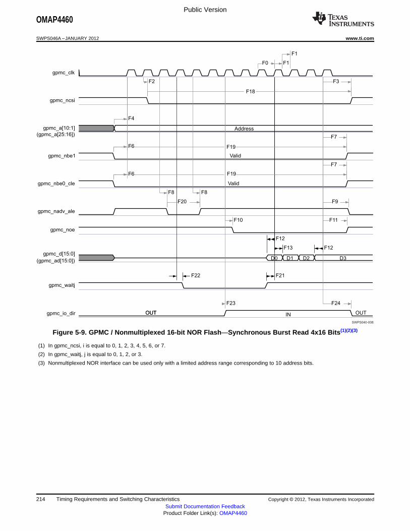
gpmc_clk
gpmc_ncsi
gpmc_a[10:1]
gpmc_nbe1
gpmc_nbe0_cle
gpmc_nadv_ale
gpmc_noe
gpmc_d[15:0]
gpmc_waitj
gpmc_io_dir
Address
Valid
Valid
D0 D1 D2 D3
OUTOUT IN OUT
F6
F2
F8 F8
F10
F13
F12
F12
F11
F9
F7
F3
F0 F1
F1
F6
F7
F22 F21
F4
F18
F20
F19
F19
F23 F24
SWPS040-008
(gpmc_ad[15:0])
(gpmc_a[25:16])
Public Version
OMAP4460
SWPS046A –JANUARY 2012 www.ti.com
Figure 5-9. GPMC / Nonmultiplexed 16-bit NOR Flash—Synchronous Burst Read 4x16 Bits(1)(2)(3)
(1) In gpmc_ncsi, i is equal to 0, 1, 2, 3, 4, 5, 6, or 7.
(2) In gpmc_waitj, j is equal to 0, 1, 2, or 3.
(3) Nonmultiplexed NOR interface can be used only with a limited address range corresponding to 10 address bits.
214 Timing Requirements and Switching Characteristics Copyright © 2012, Texas Instruments Incorporated
Submit Documentation FeedbackProduct Folder Link(s): OMAP4460

gpmc_clk
gpmc_ncsi
gpmc_a[26:17]
gpmc_nbe1
gpmc_nbe0_cle
gpmc_nadv_ale
gpmc_nwe
gpmc_a[16:1]/gpmc_d[15:0]
gpmc_waitj
gpmc_io_dir
Address (MSB)
Address (LSB) D 0 D 1 D 2 D 3
OUT
F4
F15 F15 F15
F1
F1
F2
F6
F8F8
F0
F3
F17
F17
F17
F9
F6 F17
F17
F17
F18
F20
F14
F14
F22 F21
SWPS040-009
(gpmc_ad[15:0])
(gpmc_a[25:16])
Public Version
OMAP4460
www.ti.com SWPS046A –JANUARY 2012
Figure 5-10. GPMC / Multiplexed 16-bit NOR Flash—Synchronous Burst Write 4 x 16 Bits(1)(2)
(1) In gpmc_ncsi, i is equal to 0, 1, 2, 3, 4, 5, 6, or 7.
(2) In gpmc_waitj, j is equal to 0, 1, 2, or 3.
Copyright © 2012, Texas Instruments Incorporated Timing Requirements and Switching Characteristics 215Submit Documentation Feedback
Product Folder Link(s): OMAP4460

gpmc_clk
gpmc_ncsi
(gpmc_a[25:16])
gpmc_nbe1
gpmc_nbe0_cle
gpmc_nadv_ale
gpmc_nwe
gpmc_d[15:0]
gpmc_waitj
gpmc_io_dir
Address
D 0 D 1 D 2 D 3
OUT
F4
F15 F15 F15
F1
F1
F2
F6
F8F8
F0
F3
F17
F17
F17
F9
F6 F17
F17
F17
F18
F20
F14
F14
F22 F21
SWPS040-010
gpmc_a[10:1]
(gpmc_ad[15:0])
Public Version
OMAP4460
SWPS046A –JANUARY 2012 www.ti.com
Figure 5-11. GPMC / Nonmultiplexed 16-bit NOR Flash—Synchronous Burst Write 4 x 16 Bits(1)(2)(3)
(1) In gpmc_ncsi, i is equal to 0, 1, 2, 3, 4, 5, 6, or 7.
(2) In gpmc_waitj, j is equal to 0, 1, 2, or 3.
(3) Nonmultiplexed NOR interface can be used only with a limited address range corresponding to 10 address bits.
5.4.1.3 GPMC/NOR Flash Interface—Asynchronous Mode
Table 5-10 and Table 5-11 assume testing over the recommended operating conditions and electricalcharacteristic conditions below (see Figure 5-12 through Figure 5-17).
Table 5-8. GPMC/NOR Flash Timing Conditions—Asynchronous Mode(1)(2)(3)
TIMING CONDITION PARAMETER VALUE UNIT
MIN MAX
Input Conditions
tR Input signal rise time 1.80 ns
tF Input signal fall time 1.80 ns
PCB Conditions
Number of external peripherals 1
Far end load 10 pF
Trace length 4 cm
Characteristics impedance 30 50 Ω
216 Timing Requirements and Switching Characteristics Copyright © 2012, Texas Instruments Incorporated
Submit Documentation FeedbackProduct Folder Link(s): OMAP4460

Public Version
OMAP4460
www.ti.com SWPS046A –JANUARY 2012
(1) IO settings except gpmc_nwp: LB0 = 1.For more information, see the Control Module / Control Module Functional Description/ Functional Register Description / Signal IntegrityParameter Control Registers with Pad Group Assignment section of the OMAP4460 TRM.IO settings for gpmc_nwp: MB[1:0] = 01 and LB0 = 0.For more information, see the Control Module / Control Module Functional Description/ Functional Register Description / Signal IntegrityParameter Control Registers with Pad Group Assignment / 50-Ω Output Buffer I/Os with Combined Mode and Load Settings section ofthe OMAP4460 TRM.
(2) In this table the rise and fall times are calculated for 20% to 80% of VDDS. For more information on the corresponding OMAP4 VDDSpower supply name, see Table 2-1, POWER [9] column with the ball name.
(3) To have an idea of the output OMAP4 ball load supported for this application, you can consider the following:Output OMAP4 ball load = Far End load + 1.34 pF/cm typical x trace length (cm).
Table 5-9. GPMC/NOR Flash—Asynchronous Mode—Internal Parameters
NO. PARAMETER OPP100, OPP119 OPP50 UNIT
MIN MAX MIN MAX
FI1 Max output data generation delay from internal functional clock 6.5 13.7 ns
FI2 Max input data capture delay by internal functional clock 4.0 8.1 ns
FI3 Max chip select generation delay from internal functional clock 6.5 13.7 ns
FI4 Max address generation delay from internal functional clock 6.5 13.7 ns
FI5 Max address valid generation delay from internal functional clock 6.5 13.7 ns
FI6 Max byte enable generation delay from internal functional clock 6.5 13.7 ns
FI7 Max output enable generation delay from internal functional clock 6.5 13.7 ns
FI8 Max write enable generation delay from internal functional clock 6.5 13.7 ns
FI9 Max functional clock skew 100.0 200.0 ps
FI10 Max IO direction generation delay from internal functional clock 6.5 13.7 ps
Table 5-10. GPMC/NOR Flash Timing Requirements—Asynchronous Mode(1)(2)(3)
NO. PARAMETER OPP100, OPP119 OPP50 UNIT
MIN MAX MIN MAX
FA5 tACc(DAT) Data max access time H(8) H(8) GPMC_FCLKcycles
FA20 tACC1-PGMODE(DAT) Page mode successive data max access P(15) P(15) GPMC_FCLKtime cycles
FA21 tACC2-PGMODE(DAT) Page mode first data max access time H(8) H(8) GPMC_FCLKcycles
(1) FA5 parameter illustrates amount of time required to internally sample input Data. It is expressed in number of GPMC functional clockcycles. From start of read cycle and after FA5 functional clock cycles, input Data will be internally sampled by active functional clockedge. FA5 value must be stored inside AccessTime register bits field.
(2) FA21 parameter illustrates amount of time required to internally sample first input Page Data. It is expressed in number of GPMCfunctional clock cycles. From start of read cycle and after FA21 functional clock cycles, First input Page Data will be internally sampledby active functional clock edge. FA21 value must be stored inside AccessTime register bits field.
(3) FA20 parameter illustrates amount of time required to internally sample successive input Page Data. It is expressed in number of GPMCfunctional clock cycles. After each access to input Page Data, next input Page Data will be internally sampled by active functional clockedge after FA20 functional clock cycles. FA20 value must be stored in PageBurstAccessTime register bits field.
Table 5-11. GPMC/NOR Flash Switching Characteristics—Asynchronous Mode
NO. PARAMETER OPP100, OPP119 OPP50 UNIT
MIN MAX MIN MAX
tR(DO) Rise time, output data 2 2 ns
tF(DO) Fall time, output data 2 2 ns
FA0 tw(nBEV) Pulse duration, Read N(13) N(13) nsgpmc_nbe0_cle, gpmc_nbe1 Write N(13) N(13) nsvalid time
FA1 tw(nCSV) Pulse duration, gpmc_ncsx Read A(1) A(1) nslow Write A(1) A(1) ns
Copyright © 2012, Texas Instruments Incorporated Timing Requirements and Switching Characteristics 217Submit Documentation Feedback
Product Folder Link(s): OMAP4460

Public Version
OMAP4460
SWPS046A –JANUARY 2012 www.ti.com
Table 5-11. GPMC/NOR Flash Switching Characteristics—Asynchronous Mode (continued)
NO. PARAMETER OPP100, OPP119 OPP50 UNIT
MIN MAX MIN MAX
FA3 td(nCSV-nADVIV) Delay time, gpmc_ncsx(14) Read B(2) – 0.2 B(2) + 2.0 B(2) – 0.2 B(2) + 2.6 nsvalid to gpmc_nadv_ale invalid Write B(2) – 0.2 B(2) + 2.0 B(2) – 0.2 B(2) + 2.6 ns
FA4 td(nCSV-nOEIV) Delay time, gpmc_ncsx(14) valid to C(3) – 0.2 C(3) + 2.0 C(3) – 0.2 C(3) + 2.6 nsgpmc_noe invalid (Single read)
FA9 td(AV-nCSV) Delay time, address bus valid to J(10) – 0.2 J(10) + 2.0 J(10) – 0.2 J(10) + 2.6 nsgpmc_ncsx(14) valid
FA10 td(nBEV-nCSV) Delay time, gpmc_nbe0_cle, J(10) – 0.2 J(10) + 2.0 J(10) – 0.2 J(10) + 2.6 nsgpmc_nbe1 valid to gpmc_ncsx(14) valid
FA12 td(nCSV-nADVV) Delay time, gpmc_ncsx(14) valid to K(11) – 0.2 K(11) + 2.0 K(11) – 0.2 K(11) + 2.6 nsgpmc_nadv_ale valid
FA13 td(nCSV-nOEV) Delay time, gpmc_ncsx(14) valid to L(12) – 0.2 L(12) + 2.0 L(12) – 0.2 L(12) + 2.6 nsgpmc_noe valid
FA14 td(nCSV-IODIR) Delay time, gpmc_ncsx(14) valid to L(12) – 0.2 L(12) + 2.0 L(12) – 0.2 L(12) + 2.6 nsgpmc_io_dir high
FA15 td(nCSV-IODIR) Delay time, gpmc_ncsx(14) valid to M(16) – 0.2 M(16) + 2.0 M(16) – 0.2 M(16) + 2.6 nsgpmc_io_dir low
FA16 tw(AIV) Address invalid duration between 2 G(7) G(7) nssuccessive R/W accesses
FA18 td(nCSV-nOEIV) Delay time, gpmc_ncsx(14) valid to I(9) – 0.2 I(9) + 2.0 I(9) – 0.2 I(9) + 2.6 nsgpmc_noe invalid (Burst read)
FA20 tw(AV) Pulse duration, address valid – 2nd, 3rd, D(4) D(4) nsand 4th accesses
FA25 td(nCSV-nWEV) Delay time, gpmc_ncsx(14) valid to E(5) – 0.2 E(5) + 2.0 E(5) – 0.2 E(5) + 2.6 nsgpmc_nwe valid
FA27 td(nCSV-nWEIV) Delay time, gpmc_ncsx(14) valid to F(6) – 0.2 F(6) + 2.0 F(6) – 0.2 F(6) + 2.6 nsgpmc_nwe invalid
FA28 td(nWEV-DV) Delay time, gpmc_ nwe valid to data bus 2 2.6 nsvalid
FA29 td(DV-nCSV) Delay time, data bus valid to J(10) – 0.2 J(10) + 2.0 J(10) – 0.2 J(10) + 2.6 nsgpmc_ncsx(14) valid
FA37 td(nOEV-AIV) Delay time, gpmc_noe valid to 2 2.6 nsgpmc_a[16:1] address phase end
(1) For single read: A = (CSRdOffTime – CSOnTime) * (TimeParaGranularity + 1) * GPMC_FCLKFor single write: A = (CSWrOffTime – CSOnTime) * (TimeParaGranularity + 1) * GPMC_FCLKFor burst read: A = (CSRdOffTime – CSOnTime + (n – 1) * PageBurstAccessTime) * (TimeParaGranularity + 1) * GPMC_FCLK with nthe page burst access numberFor burst write: A = (CSWrOffTime – CSOnTime + (n – 1) * PageBurstAccessTime) * (TimeParaGranularity + 1) * GPMC_FCLK with nthe page burst access number
(2) For reading: B = ((ADVRdOffTime – CSOnTime) * (TimeParaGranularity + 1) + 0.5 * (ADVExtraDelay – CSExtraDelay)) * GPMC_FCLKFor writing: B = ((ADVWrOffTime – CSOnTime) * (TimeParaGranularity + 1) + 0.5 * (ADVExtraDelay – CSExtraDelay)) * GPMC_FCLK
(3) C = ((OEOffTime – CSOnTime) * (TimeParaGranularity + 1) + 0.5 * (OEExtraDelay – CSExtraDelay)) * GPMC_FCLK
(4) D = PageBurstAccessTime * (TimeParaGranularity + 1) * GPMC_FCLK
(5) E = ((WEOnTime – CSOnTime) * (TimeParaGranularity + 1) + 0.5 * (WEExtraDelay – CSExtraDelay)) * GPMC_FCLK
(6) F = ((WEOffTime – CSOnTime) * (TimeParaGranularity + 1) + 0.5 * (WEExtraDelay – CSExtraDelay)) * GPMC_FCLK
(7) G = Cycle2CycleDelay * GPMC_FCLK
(8) H = AccessTime * (TimeParaGranularity + 1)
(9) I = ((OEOffTime + (n – 1) * PageBurstAccessTime – CSOnTime) * (TimeParaGranularity + 1) + 0.5 * (OEExtraDelay – CSExtraDelay)) *GPMC_FCLK
(10) J = (CSOnTime * (TimeParaGranularity + 1) + 0.5 * CSExtraDelay) * GPMC_FCLK
(11) K = ((ADVOnTime – CSOnTime) * (TimeParaGranularity + 1) + 0.5 * (ADVExtraDelay – CSExtraDelay)) * GPMC_FCLK
(12) L = ((OEOnTime – CSOnTime) * (TimeParaGranularity + 1) + 0.5 * (OEExtraDelay – CSExtraDelay)) * GPMC_FCLK
(13) For single read: N = RdCycleTime * (TimeParaGranularity + 1) * GPMC_FCLKFor single write: N = WrCycleTime * (TimeParaGranularity + 1) * GPMC_FCLKFor burst read: N = (RdCycleTime + (n – 1) * PageBurstAccessTime) * (TimeParaGranularity + 1) * GPMC_FCLKFor burst write: N = (WrCycleTime + (n – 1) * PageBurstAccessTime) * (TimeParaGranularity + 1) * GPMC_FCLK
218 Timing Requirements and Switching Characteristics Copyright © 2012, Texas Instruments Incorporated
Submit Documentation FeedbackProduct Folder Link(s): OMAP4460
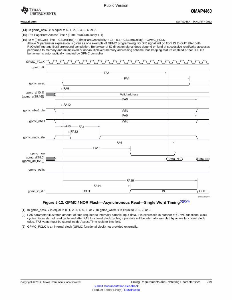
GPMC_FCLK
gpmc_clk
gpmc_ncsx
(gpmc_a[25:16])
gpmc_nbe0_cle
gpmc_nbe1
gpmc_nadv_ale
gpmc_noe
gpmc_d[15:0]
gpmc_waitx
gpmc_io_dir
Valid address
Valid
Valid
Data IN 0 Data IN 0
OUTOUT IN OUT
FA0
FA9
FA10
FA3
FA1
FA4
FA12
FA13
FA0
FA10
FA5
FA14
FA15
SWPS040-011
gpmc_a[10:1]
(gpmc_ad[15:0])
Public Version
OMAP4460
www.ti.com SWPS046A –JANUARY 2012
(14) In gpmc_ncsx, x is equal to 0, 1, 2, 3, 4, 5, 6, or 7.
(15) P = PageBurstAccessTime * (TimeParaGranularity + 1)
(16) M = ((RdCycleTime – CSOnTime) * (TimeParaGranularity + 1) – 0.5 * CSExtraDelay) * GPMC_FCLKAbove M parameter expression is given as one example of GPMC programming. IO DIR signal will go from IN to OUT after bothRdCycleTime and BusTurnAround completion. Behaviour of IO direction signal does depend on kind of successive read/write accessesperformed to memory and multiplexed or non/multiplexed memory addressing scheme, bus keeping feature enabled or not. IO DIRbehaviour is automactically handled by GPMC controller
Figure 5-12. GPMC / NOR Flash—Asynchronous Read—Single Word Timing(1)(2)(3)
(1) In gpmc_ncsx, x is equal to 0, 1, 2, 3, 4, 5, 6, or 7. In gpmc_waitx, x is equal to 0, 1, 2, or 3.
(2) FA5 parameter illustrates amount of time required to internally sample input data. It is expressed in number of GPMC functional clockcycles. From start of read cycle and after FA5 functional clock cycles, input data will be internally sampled by active functional clockedge. FA5 value must be stored inside AccessTime register bits field.
(3) GPMC_FCLK is an internal clock (GPMC functional clock) not provided externally.
Copyright © 2012, Texas Instruments Incorporated Timing Requirements and Switching Characteristics 219Submit Documentation Feedback
Product Folder Link(s): OMAP4460

GPMC_FCLK
gpmc_clk
gpmc_ncsx
gpmc_a[10:1]
gpmc_nbe0_cle
gpmc_nbe1
gpmc_nadv_ale
gpmc_noe
gpmc_d[15:0]
gpmc_waitx
gpmc_io_dir
Address 0 Address 1
Valid Valid
Valid Valid
Data upper
OUTOUT IN OUT IN
FA9
FA10
FA3
FA9
FA3
FA13 FA13
FA1 FA1
FA4 FA4
FA12 FA12
FA10
FA0 FA0
FA16
FA0 FA0
FA10 FA10
FA5 FA5
FA14
FA15
FA14
FA15
SWPS040-012
(gpmc_a[25:16])
(gpmc_ad[15:0])
Public Version
OMAP4460
SWPS046A –JANUARY 2012 www.ti.com
Figure 5-13. GPMC / NOR Flash—Asynchronous Read—32-bit Timing(1)(2)(3)
(1) In gpmc_ncsx, x is equal to 0, 1, 2, 3, 4, 5, 6, or 7. In gpmc_waitx, x is equal to 0, 1, 2, or 3.
(2) FA5 parameter illustrates amount of time required to internally sample input data. It is expressed in number of GPMC functional clockcycles. From start of read cycle and after FA5 functional clock cycles, input Data will be internally sampled by active functional clockedge. FA5 value must be stored inside AccessTime register bits field.
(3) GPMC_FCLK is an internal clock (GPMC functional clock) not provided externally.
220 Timing Requirements and Switching Characteristics Copyright © 2012, Texas Instruments Incorporated
Submit Documentation FeedbackProduct Folder Link(s): OMAP4460
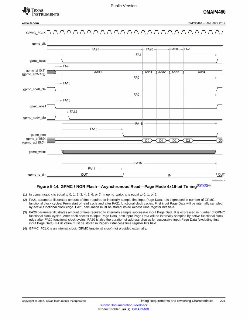
GPMC_FCLK
gpmc_clk
gpmc_ncsx
gpmc_a[10:1]
gpmc_nbe0_cle
gpmc_nbe1
gpmc_nadv_ale
gpmc_noe
gpmc_d[15:0]
gpmc_waitx
gpmc_io_dir
Add0 Add1 Add2 Add3 Add4
D0 D1 D2 D3 D3
OUTOUT IN OUT
FA1
FA0
FA18
FA13
FA12
FA0
FA9
FA10
FA10
FA21 FA20 FA20 FA20
FA14
FA15
SWPS040-013
(gpmc_a[25:16])
(gpmc_ad[15:0])
Public Version
OMAP4460
www.ti.com SWPS046A –JANUARY 2012
Figure 5-14. GPMC / NOR Flash—Asynchronous Read—Page Mode 4x16-bit Timing(1)(2)(3)(4)
(1) In gpmc_ncsx, x is equal to 0, 1, 2, 3, 4, 5, 6, or 7. In gpmc_waitx, x is equal to 0, 1, or 2.
(2) FA21 parameter illustrates amount of time required to internally sample first input Page Data. It is expressed in number of GPMCfunctional clock cycles. From start of read cycle and after FA21 functional clock cycles, First input Page Data will be internally sampledby active functional clock edge. FA21 calculation must be stored inside AccessTime register bits field.
(3) FA20 parameter illustrates amount of time required to internally sample successive input Page Data. It is expressed in number of GPMCfunctional clock cycles. After each access to input Page Data, next input Page Data will be internally sampled by active functional clockedge after FA20 functional clock cycles. FA20 is also the duration of address phases for successive input Page Data (excluding firstinput Page Data). FA20 value must be stored in PageBurstAccessTime register bits field.
(4) GPMC_FCLK is an internal clock (GPMC functional clock) not provided externally.
Copyright © 2012, Texas Instruments Incorporated Timing Requirements and Switching Characteristics 221Submit Documentation Feedback
Product Folder Link(s): OMAP4460

gpmc_fclk
gpmc_clk
gpmc_ncsx
gpmc_a[10:1]
gpmc_nbe0_cle
gpmc_nbe1
gpmc_nadv_ale
gpmc_nwe
(gpmc_ad[15:0])
gpmc_waitx
gpmc_io_dir
Valid address
Data OUT
OUT
FA0
FA1
FA10
FA3
FA25
FA29
FA9
FA12
FA27
FA0
FA10
SWPS040-014
(gpmc_a[25:16])
gpmc_d[15:0]
Public Version
OMAP4460
SWPS046A –JANUARY 2012 www.ti.com
Figure 5-15. GPMC / NOR Flash—Asynchronous Write—Single Word Timing(1)
(1) In gpmc_ncsx, x is equal to 0, 1, 2, 3, 4, 5, 6, or 7. In gpmc_waitx, x is equal to 0, 1, or 2.
222 Timing Requirements and Switching Characteristics Copyright © 2012, Texas Instruments Incorporated
Submit Documentation FeedbackProduct Folder Link(s): OMAP4460
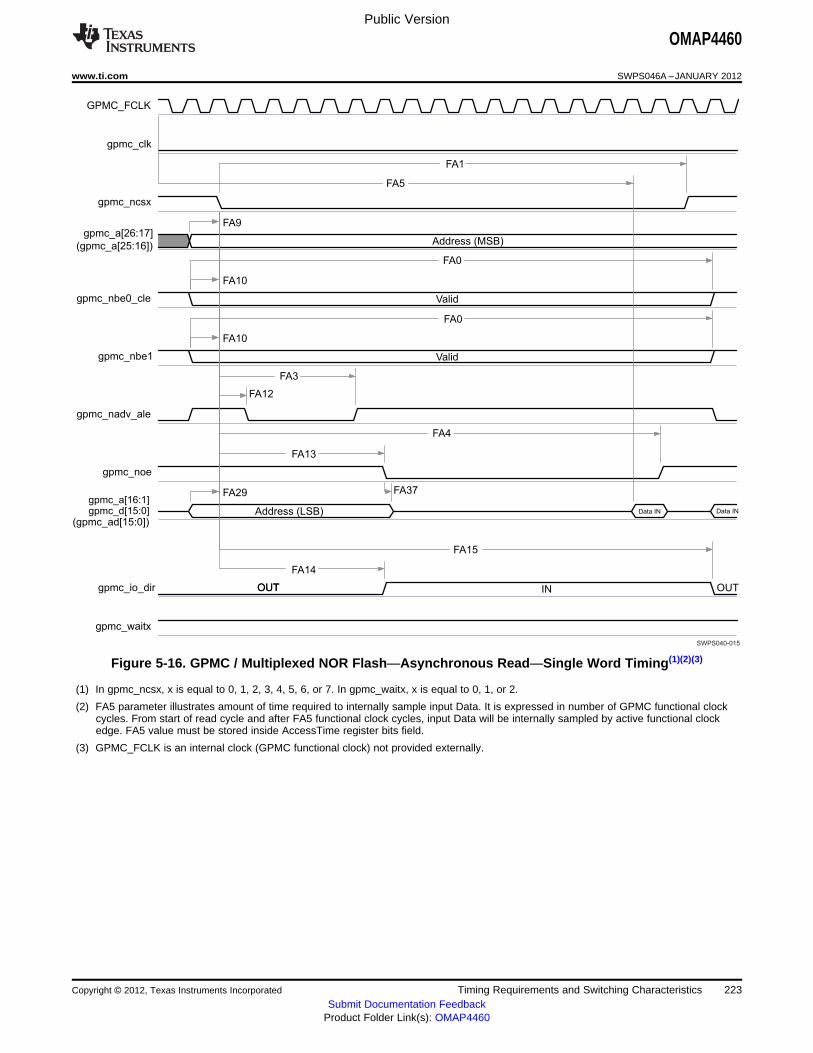
GPMC_FCLK
gpmc_clk
gpmc_ncsx
(gpmc_a[25:16])
gpmc_nbe0_cle
gpmc_nbe1
gpmc_nadv_ale
gpmc_noe
gpmc_io_dir
gpmc_waitx
Address (MSB)
Valid
Valid
Address (LSB) Data IN Data IN
OUTOUT IN OUT
FA0
FA9
FA10
FA3
FA13
FA29
FA1
FA37
FA12
FA4
FA10
FA0
FA5
FA14
FA15
SWPS040-015
gpmc_a[16:1]gpmc_d[15:0]
(gpmc_ad[15:0])
gpmc_a[26:17]
Public Version
OMAP4460
www.ti.com SWPS046A –JANUARY 2012
Figure 5-16. GPMC / Multiplexed NOR Flash—Asynchronous Read—Single Word Timing(1)(2)(3)
(1) In gpmc_ncsx, x is equal to 0, 1, 2, 3, 4, 5, 6, or 7. In gpmc_waitx, x is equal to 0, 1, or 2.
(2) FA5 parameter illustrates amount of time required to internally sample input Data. It is expressed in number of GPMC functional clockcycles. From start of read cycle and after FA5 functional clock cycles, input Data will be internally sampled by active functional clockedge. FA5 value must be stored inside AccessTime register bits field.
(3) GPMC_FCLK is an internal clock (GPMC functional clock) not provided externally.
Copyright © 2012, Texas Instruments Incorporated Timing Requirements and Switching Characteristics 223Submit Documentation Feedback
Product Folder Link(s): OMAP4460

FA12
FA27
FA28
FA0
FA10
gpmc_fclk
gpmc_clk
gpmc_ncsx
gpmc_a[26:17]
gpmc_nbe0_cle
gpmc_nbe1
gpmc_nadv_ale
gpmc_nwe
(gpmc_ad[15:0])
gpmc_waitx
gpmc_io_dir
Address (MSB)
Valid address (LSB) Data OUT
OUT
FA0
FA1
FA9
FA10
FA3
FA25
FA29gpmc_a[16:1]/
SWPS040-016
gpmc_d[15:0]
(gpmc_a[25:16])
Public Version
OMAP4460
SWPS046A –JANUARY 2012 www.ti.com
Figure 5-17. GPMC / Multiplexed NOR Flash—Asynchronous Write—Single Word Timing(1)
(1) In gpmc_ncsx, x is equal to 0, 1, 2, 3, 4, 5, 6, or 7. In gpmc_waitx, x is equal to 0, 1, or 2.
5.4.1.4 GPMC/NAND Flash Interface—Asynchronous Mode
Table 5-14 and Table 5-15 assume testing over the recommended operating conditions and electricalcharacteristic conditions below (see Figure 5-18 through Figure 5-21).
Table 5-12. GPMC/NAND Flash Timing Conditions—Asynchronous Mode(1)(2)(3)
TIMING CONDITION PARAMETER VALUE UNIT
MIN MAX
Input Conditions
tR Input signal rise time 1.80 ns
tF Input signal fall time 1.80 ns
PCB Conditions
Number of external peripherals 1
Far end load 10 pF
Trace length 4 cm
Characteristics impedance 30 50 Ω
224 Timing Requirements and Switching Characteristics Copyright © 2012, Texas Instruments Incorporated
Submit Documentation FeedbackProduct Folder Link(s): OMAP4460
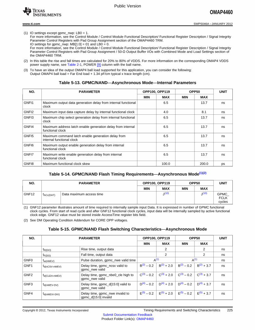
Public Version
OMAP4460
www.ti.com SWPS046A –JANUARY 2012
(1) IO settings except gpmc_nwp: LB0 = 1.For more information, see the Control Module / Control Module Functional Description/ Functional Register Description / Signal IntegrityParameter Control Registers with Pad Group Assignment section of the OMAP4460 TRM.IO settings for gpmc_nwp: MB[1:0] = 01 and LB0 = 0.For more information, see the Control Module / Control Module Functional Description/ Functional Register Description / Signal IntegrityParameter Control Registers with Pad Group Assignment / 50-Ω Output Buffer I/Os with Combined Mode and Load Settings section ofthe OMAP4460 TRM.
(2) In this table the rise and fall times are calculated for 20% to 80% of VDDS. For more information on the corresponding OMAP4 VDDSpower supply name, see Table 2-1, POWER [9] column with the ball name.
(3) To have an idea of the output OMAP4 ball load supported for this application, you can consider the following:Output OMAP4 ball load = Far End load + 1.34 pF/cm typical x trace length (cm).
Table 5-13. GPMC/NAND—Asynchronous Mode—Internal Parameters
NO. PARAMETER OPP100, OPP119 OPP50 UNIT
MIN MAX MIN MAX
GNFI1 Maximum output data generation delay from internal functional 6.5 13.7 nsclock
GNFI2 Maximum input data capture delay by internal functional clock 4.0 8.1 ns
GNFI3 Maximum chip select generation delay from internal functional 6.5 13.7 nsclock
GNFI4 Maximum address latch enable generation delay from internal 6.5 13.7 nsfunctional clock
GNFI5 Maximum command latch enable generation delay from 6.5 13.7 nsinternal functional clock
GNFI6 Maximum output enable generation delay from internal 6.5 13.7 nsfunctional clock
GNFI7 Maximum write enable generation delay from internal 6.5 13.7 nsfunctional clock
GNFI8 Maximum functional clock skew 100.0 200.0 ps
Table 5-14. GPMC/NAND Flash Timing Requirements—Asynchronous Mode(1)(2)
NO. PARAMETER OPP100, OPP119 OPP50 UNIT
MIN MAX MIN MAX
GNF12 tACc(DAT) Data maximum access time J(10) J(10) GPMC_FCLKcycles
(1) GNF12 parameter illustrates amount of time required to internally sample input Data. It is expressed in number of GPMC functionalclock cycles. From start of read cycle and after GNF12 functional clock cycles, input data will be internally sampled by active functionalclock edge. GNF12 value must be stored inside AccessTime register bits field.
(2) See DM Operating Condition Addendum for CORE OPP voltages.
Table 5-15. GPMC/NAND Flash Switching Characteristics—Asynchronous Mode
NO. PARAMETER OPP100, OPP119 OPP50 UNIT
MIN MAX MIN MAX
tR(DO) Rise time, output data 2 2 ns
tF(DO) Fall time, output data 2 2 ns
GNF0 tw(nWEV) Pulse duration, gpmc_nwe valid time A(1) A(1) ns
GNF1 td(nCSV-nWEV) Delay time, gpmc_ncsx valid to B(2) – 0.2 B(2) + 2.0 B(2) – 0.2 B(2) + 3.7 nsgpmc_nwe valid
GNF2 td(CLEH-nWEV) Delay time, gpmc_nbe0_cle high to C(3) – 0.2 C(3) + 2.0 C(3) – 0.2 C(3) + 3.7 nsgpmc_nwe valid
GNF3 td(nWEV-DV) Delay time, gpmc_d[15:0] valid to D(4) – 0.2 D(4) + 2.0 D(4) – 0.2 D(4) + 3.7 nsgpmc_nwe valid
GNF4 td(nWEIV-DIV) Delay time, gpmc_nwe invalid to E(5) – 0.2 E(5) + 2.0 E(5) – 0.2 E(5) + 3.7 nsgpmc_d[15:0] invalid
Copyright © 2012, Texas Instruments Incorporated Timing Requirements and Switching Characteristics 225Submit Documentation Feedback
Product Folder Link(s): OMAP4460

GPMC_FCLK
gpmc_ncsx
gpmc_nbe0_cle
gpmc_nadv_ale
gpmc_noe
gpmc_nwe
(gpmc_ad[15:0]) Command
GNF0
GNF1
GNF2
GNF3 GNF4
GNF5
GNF6
SWPS040-017
gpmc_d[15:0]
Public Version
OMAP4460
SWPS046A –JANUARY 2012 www.ti.com
Table 5-15. GPMC/NAND Flash Switching Characteristics—Asynchronous Mode (continued)
NO. PARAMETER OPP100, OPP119 OPP50 UNIT
MIN MAX MIN MAX
GNF5 td(nWEIV-CLEIV) Delay time, gpmc_nwe invalid to F(6) – 0.2 F(6) + 2.0 F(6) – 0.2 F(6) + 3.7 nsgpmc_nbe0_cle invalid
GNF6 td(nWEIV-nCSIV) Delay time, gpmc_nwe invalid to G(7) – 0.2 G(7) + 2.0 G(7) – 0.2 G(7) + 3.7 nsgpmc_ncsx invalid
GNF7 td(ALEH-nWEV) Delay time, gpmc_nadv_ale high to C(3) – 0.2 C(3) + 2.0 C(3) – 0.2 C(3) + 3.7 nsgpmc_nwe valid
GNF8 td(nWEIV-ALEIV) Delay time, gpmc_nwe invalid to F(6) – 0.2 F(6) + 2.0 F(6) – 0.2 F(6) + 3.7 nsgpmc_nadv_ale invalid
GNF9 tc(nWE) Cycle time, Write cycle time H(8) H(8) ns
GNF10 td(nCSV-nOEV) Delay time, gpmc_ncsx valid to I(9) – 0.2 I(9) + 2.0 I(9) – 0.2 I(9) + 3.7 nsgpmc_noe valid
GNF13 tw(nOEV) Pulse duration, gpmc_noe valid time K(11) K(11) ns
GNF14 tc(nOE) Cycle time, read cycle time L(12) L(12) ns
GNF15 td(nOEIV-nCSIV) Delay time, gpmc_noe invalid to M(13) – 0.2 M(13) + 2.0 M(13) – 0.2 M(13) + 3.7 nsgpmc_ncsx invalid
(1) A = (WEOffTime – WEOnTime) * (TimeParaGranularity + 1) * GPMC_FCLK
(2) B = ((WEOnTime – CSOnTime) * (TimeParaGranularity + 1) + 0.5 * (WEExtraDelay – CSExtraDelay)) * GPMC_FCLK
(3) C = ((WEOnTime – ADVOnTime) * (TimeParaGranularity + 1) + 0.5 * (WEExtraDelay – ADVExtraDelay)) * GPMC_FCLK
(4) D = (WEOnTime * (TimeParaGranularity + 1) + 0.5 * WEExtraDelay ) * GPMC_FCLK
(5) E = ((WrCycleTime – WEOffTime) * (TimeParaGranularity + 1) – 0.5 * WEExtraDelay ) * GPMC_FCLK
(6) F = ((ADVWrOffTime – WEOffTime) * (TimeParaGranularity + 1) + 0.5 * (ADVExtraDelay – WEExtraDelay )) * GPMC_FCLK
(7) G = ((CSWrOffTime – WEOffTime) * (TimeParaGranularity + 1) + 0.5 * (CSExtraDelay – WEExtraDelay )) * GPMC_FCLK
(8) H = WrCycleTime * (1 + TimeParaGranularity) * GPMC_FCLK
(9) I = ((OEOnTime – CSOnTime) * (TimeParaGranularity + 1) + 0.5 * (OEExtraDelay – CSExtraDelay)) * GPMC_FCLK
(10) J = AccessTime * (TimeParaGranularity + 1)
(11) K = (OEOffTime – OEOnTime) * (1 + TimeParaGranularity) * GPMC_FCLK
(12) L = RdCycleTime * (1 + TimeParaGranularity) * GPMC_FCLK
(13) M = ((CSRdOffTime – OEOffTime) * (TimeParaGranularity + 1) + 0.5 * (CSExtraDelay – OEExtraDelay ))* GPMC_FCLK
(14) In gpmc_ncsx, x is equal to 0, 1, 2, 3, 4, 5, 6, or 7.
Figure 5-18. GPMC / NAND Flash—Asynchronous Mode—Command Latch Cycle Timing(1)
(1) In gpmc_ncsx, x is equal to 0, 1, 2, 3, 4, 5, 6, or 7.
226 Timing Requirements and Switching Characteristics Copyright © 2012, Texas Instruments Incorporated
Submit Documentation FeedbackProduct Folder Link(s): OMAP4460
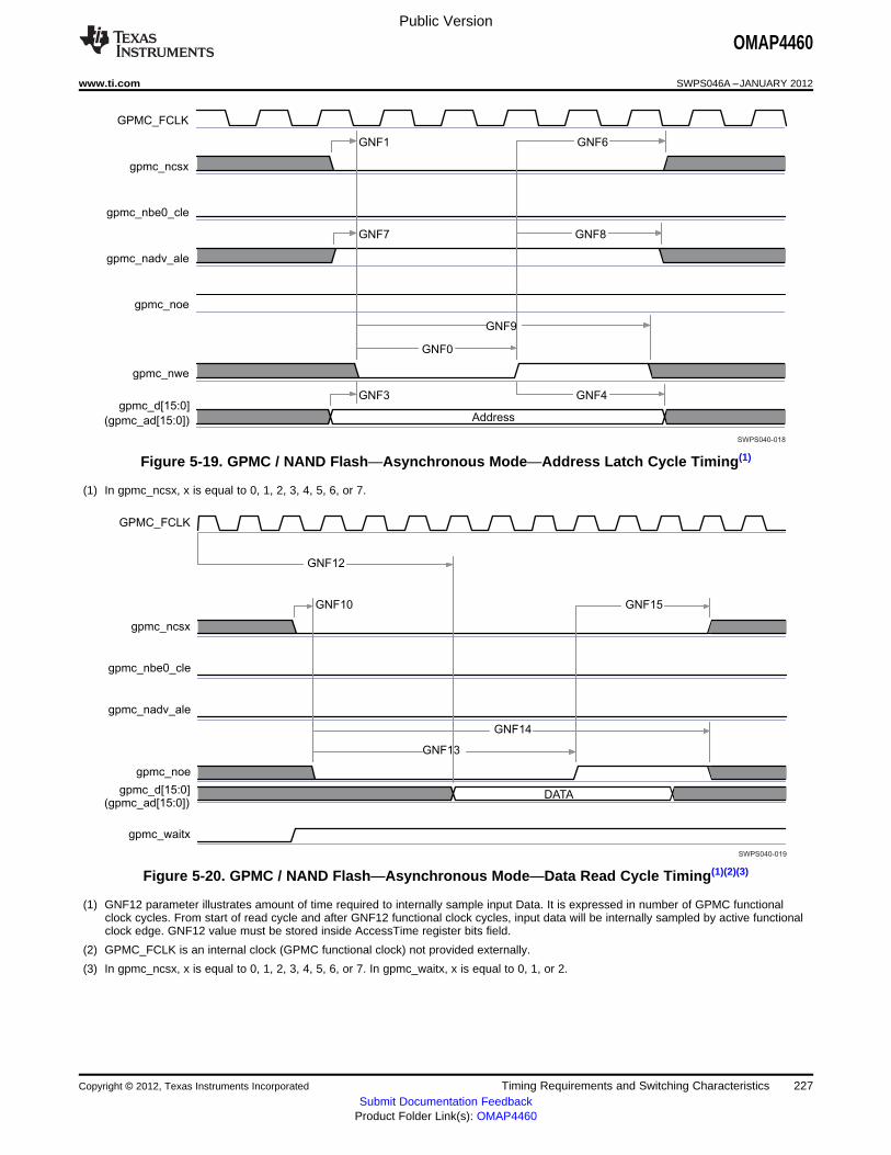
GPMC_FCLK
gpmc_ncsx
gpmc_nbe0_cle
gpmc_nadv_ale
gpmc_noe
gpmc_nwe
(gpmc_ad[15:0]) Address
GNF0
GNF1
GNF7
GNF3 GNF4
GNF6
GNF8
GNF9
SWPS040-018
gpmc_d[15:0]
GPMC_FCLK
gpmc_ncsx
gpmc_nbe0_cle
gpmc_nadv_ale
gpmc_noe
(gpmc_ad[15:0])
gpmc_waitx
DATA
GNF10
GNF13
GNF14
GNF15
GNF12
SWPS040-019
gpmc_d[15:0]
Public Version
OMAP4460
www.ti.com SWPS046A –JANUARY 2012
Figure 5-19. GPMC / NAND Flash—Asynchronous Mode—Address Latch Cycle Timing(1)
(1) In gpmc_ncsx, x is equal to 0, 1, 2, 3, 4, 5, 6, or 7.
Figure 5-20. GPMC / NAND Flash—Asynchronous Mode—Data Read Cycle Timing(1)(2)(3)
(1) GNF12 parameter illustrates amount of time required to internally sample input Data. It is expressed in number of GPMC functionalclock cycles. From start of read cycle and after GNF12 functional clock cycles, input data will be internally sampled by active functionalclock edge. GNF12 value must be stored inside AccessTime register bits field.
(2) GPMC_FCLK is an internal clock (GPMC functional clock) not provided externally.
(3) In gpmc_ncsx, x is equal to 0, 1, 2, 3, 4, 5, 6, or 7. In gpmc_waitx, x is equal to 0, 1, or 2.
Copyright © 2012, Texas Instruments Incorporated Timing Requirements and Switching Characteristics 227Submit Documentation Feedback
Product Folder Link(s): OMAP4460

GPMC_FCLK
gpmc_ncsx
gpmc_nbe0_cle
gpmc_nadv_ale
gpmc_noe
gpmc_nwe
(gpmc_ad[15:0]) DATA
GNF0
GNF1
GNF4
GNF9
GNF3
GNF6
SWPS040-020
gpmc_d[15:0]
Public Version
OMAP4460
SWPS046A –JANUARY 2012 www.ti.com
Figure 5-21. GPMC / NAND Flash—Asynchronous Mode—Data Write Cycle Timing(1)
(1) In gpmc_ncsx, x is equal to 0, 1, 2, 3, 4, 5, 6, or 7.
5.4.2 External Memory Interface (EMIF)
NOTEFor more information, see the EMIF Controller section of the OMAP4460 TRM.
The SDRAM controller subsystem module provides connectivity between the processor and externalDRAM memory components. The module includes support for double-data-rate SDRAM (mobile DDR).
5.4.2.1 EMIF—DDR Mode
Table 5-17 and Table 5-18 assume testing over the recommended operating conditions and electricalcharacteristic conditions below (see Figure 5-22 through Figure 5-43). For timing parameterscorrespondence with JEDEC standard, see Table 5-19 and Table 5-20.
Table 5-16. EMIF Timing Conditions—DDR Mode
TIMING CONDITION PARAMETER VALUE UNIT
MIN MAX
Input Conditions
tR Input rise time 0.4 ns
tF Input fall time 0.4 ns
Output Condition
CLOAD Output load capacitance(1) 2 5 pF
(1) IO settings: sr[1:0] = 11.For more information, see the Control Module / Control Module Functional Description/ Functional Register Description / Signal IntegrityParameter Control Registers with Pad Group Assignment / High-speed I/O Buffers with Impedance, Slew Rate and Weak DriverSettings section of the OMAP4460 TRM.
228 Timing Requirements and Switching Characteristics Copyright © 2012, Texas Instruments Incorporated
Submit Documentation FeedbackProduct Folder Link(s): OMAP4460
Public Version
OMAP4460
www.ti.com SWPS046A –JANUARY 2012
Table 5-17. EMIF Timing Requirements—DDR Mode(3)(4)
NO. PARAMETER OPP100, OPP119 OPP50 UNIT
MIN MAX MIN MAX
DQ/DM/DQS Read Parameters
tdc(DQSI) Duty cycle error, input clock –125 125 –125 125 pslpddr2_ndqsX(1)
tj(DQSI) Jitter standard deviation, input clock 0 0 0 0 pslpddr2_ndqsX(1)
DD300 tc(DQSI) Cycle time, lpddr2_dqsX(1) and 2.5 5 nslpddr2_ndqsX(1)
DD301 tw(DQSIH) Pulse duration, lpddr2_dqsX(1) and 0.38 0.55 0.38 0.55 DD100lpddr2_ndqsX(1) high duration
DD301 tw(DQSIL) Pulse duration, lpddr2_dqsX(1) and 0.38 0.55 0.38 0.55 DD100lpddr2_ndqsX(1) low duration
DD303 td(DV-DQSI) Delay time, lpddr2_dqsX(1) input 2.2 6.0 2.1 6.1 nstransition after lpddr2_ck outputtransition
DD304 tsu(DV-DQSI) Setup time, lpddr2_dqY data valid –0.28 –0.28 nsbefore lpddr2_dqsX(1) reading transition
DD305 th(DQSI-DIV) Hold time, lpddr2_dqY data valid after 0.38 * DD100 – 0.38 * DD100 – nslpddr2_dqsX(1) reading transition 0.28 0.48
DD306 td(DQSIHZ- Delay time, lpddr2_dqsX(1) low 0.9 0.9 DD100DQSILZ) impedance before lpddr2_dqsX(1) first
transition
DD307 td(DQSILZ- Delay time, lpddr2_dqsX(1) high 0.38 0.38 DD100DQSIHZ) impedance after lpddr2_dqsX(1) last
transition
DD308 td(DQSILZ- Delay time, lpddr2_dqsX(1) driven after 2.20 2.20 nsCLKH) lpddr2_ck transition
DD309 td(DQILZ- Delay time, lpddr2_dqY driven after 2.11 1.87 nsCLKH) lpddr2_ck transition
DD310 td(clkH- Delay time, lpddr2_dqsX(1) high 5.4 5.4 nsDQSIHZ) impedance after lpddr2_ck transition
DD311 td(clkH-DQIHZ) Delay time, lpddr2_dqY high impedance 5.84 6.06 nsafter lpddr2_ck transition
DQ/DM/DQS Boot Read Parameters
DD303b tdb(DV-DQSI) Delay time, lpddr2_dqsX(1) input 2.2 6.0 2.1 6.1 nstransition after lpddr2_ck outputtransition
DD304b tsub(DV-DQSI) Setup time, lpddr2_dqY data valid 1.2 1.2 nsbefore lpddr2_dqsX(1) reading transition
DD305b thb(DQSI-DIV) Hold time, lpddr2_dqY data valid after 0.45 * DD100 – 0.45 * DD100 – nslpddr2_dqsX(1) reading transition 1.2 1.2
(1) X = [3:0]
(2) Y = [31:0]
(3) In this table, LPDDR2 means LPDDR21 and LPDDR22. For more information, see Table 2-4.
(4) See DM Operating Condition Addendum for CORE OPP voltages.
Copyright © 2012, Texas Instruments Incorporated Timing Requirements and Switching Characteristics 229Submit Documentation Feedback
Product Folder Link(s): OMAP4460
Public Version
OMAP4460
SWPS046A –JANUARY 2012 www.ti.com
Table 5-18. EMIF Switching Characteristics—DDR Mode(5)(6)
NO. PARAMETER OPP100, OPP119 OPP50 UNIT
MIN MAX MIN MAX
Output Clocks Parameters
tdc(clk) Duty cycle error, output clock lpddr2_ck –31 31 –63 63 psand lpddr2_nck
tj(clk) Jitter standard deviation, output clock –63 63 –125 125 pslpddr2_ck and lpddr2_nck
tdc(DQS) Duty cycle error, output clock –31 31 –63 63 pslpddr2_dqsX(1) and lpddr2_ndqsX(1)
tj(DQS) Jitter standard deviation, output clock –63 63 –125 125 pslpddr2_dqsX(1) and lpddr2_ndqsX(1)
tR(O) Output signal rise time 400 400 ps
tF(O) Output signal fall time 400 400 ps
DD100 tc(clk) Cycle time, lpddr2_ck and lpddr2_nck 2.5 5 ns
DD101 tw(clkH) Typical pulse duration, lpddr2_ck and 0.45 0.55 0.45 0.55 DD100lpddr2_nck high duration
DD101 tw(clkL) Typical pulse duration, lpddr2_ck and 0.45 0.55 0.45 0.55 DD100lpddr2_nck low duration
CKE and Command Address Write Parameters
DD200 tw(CKE) Pulse duration, lpddr2_cke high and low 3 * DD100 3 * DD100 nsduration
DD201 td(clkL-CKE) Delay time, lpddr2_ck low to lpddr2_cke 0.05 0.16 * 0.05 0.16 * nsDD100 – DD100 –
0.05 0.05
DD202 td(clkL-NCS) Delay time, lpddr2_ck low to lpddr2_ncs 0.34 0.41 * 0.34 0.41 * nsDD100 – DD100 –
0.34 0.34
DD203 td(clk-CA) Delay time, lpddr2_ck low to 0.29 DD101 – 0.6 DD101 – nslpddr2_caZ(3) 0.29 0.6
DD204 tw(CA) Pulse duration, lpddr2_caZ(3) high and 0.50 0.50 DD100low duration
CKE and Command Boot Write Parameters
DD200b tcb(clk) Cycle time, lpddr2_ck and lpddr2_nck 2.5 5 ns
DD201b tdb(clkL-CKE) Delay time, lpddr2_ck low to lpddr2_cke 0.05 0.16 * 0.05 0.16 * nsDD100 – DD100 –
0.05 0.05
DD202b tdb(clkL-NCS) Delay time, lpddr2_ck low to lpddr2_ncs 0.34 0.41 * 0.34 0.41 * nsDD100 – DD100 –
0.34 0.34
DD203b tdb(clk-CA) Delay time, lpddr2_ck low to 1.15 DD101 – 1.15 DD101 – nslpddr2_caZ(3) 1.15 1.15
DQ/DM/DQS Write Parameters
DD400 tc(DQSO) Cycle time, lpddr2_dqsX(1) and 2.5 5 nslpddr2_ndqsX(1)
DD401 tw(DQSOH) Pulse duration, lpddr2_dqsX(1) and 0.5 0.5 0.5 0.5 DD400lpddr2_ndqsX(1) high duration
DD401 tw(DQSOL) Pulse duration, lpddr2_dqsX(1) and 0.5 0.5 0.5 0.5 DD400lpddr2_ndqsX(1) low duration
DD403 td(DQSO- Delay time, lpddr2_dqsX(1) to 0.27 DD101 – 0.48 DD101 – nsDQO/DM) lpddr2_dqY(2) and lpddr2_dmX(1) 0.27 0.48
DD404 td(CLK-DQSO) Delay time, lpddr2_ck valid to 0.2 * DD100 DD101 – 0.2 * DD100 DD101 – nslpddr2_dqsX(1) falling edge 0.2 * DD100 0.2 * DD100
DD405 td(clkV-DQSO) Delay time, lpddr2_ck valid to first 0.75 1.25 0.75 1.25 DD100lpddr2_dqsX(1) edge
DD406 td(DQSOHZ- Delay time, lpddr2_dqsX(1) high 0.35 0.35 DD100DQSOV) impedance to lpddr2_dqsX(1) valid
230 Timing Requirements and Switching Characteristics Copyright © 2012, Texas Instruments Incorporated
Submit Documentation FeedbackProduct Folder Link(s): OMAP4460
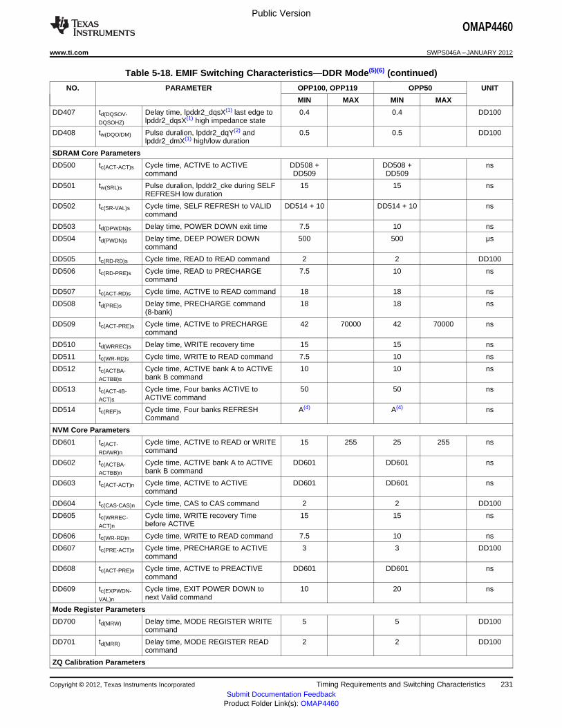
Public Version
OMAP4460
www.ti.com SWPS046A –JANUARY 2012
Table 5-18. EMIF Switching Characteristics—DDR Mode(5)(6) (continued)
NO. PARAMETER OPP100, OPP119 OPP50 UNIT
MIN MAX MIN MAX
DD407 td(DQSOV- Delay time, lpddr2_dqsX(1) last edge to 0.4 0.4 DD100DQSOHZ) lpddr2_dqsX(1) high impedance state
DD408 tw(DQO/DM) Pulse duralion, lpddr2_dqY(2) and 0.5 0.5 DD100lpddr2_dmX(1) high/low duration
SDRAM Core Parameters
DD500 tc(ACT-ACT)s Cycle time, ACTIVE to ACTIVE DD508 + DD508 + nscommand DD509 DD509
DD501 tw(SRL)s Pulse duralion, lpddr2_cke during SELF 15 15 nsREFRESH low duration
DD502 tc(SR-VAL)s Cycle time, SELF REFRESH to VALID DD514 + 10 DD514 + 10 nscommand
DD503 td(DPWDN)s Delay time, POWER DOWN exit time 7.5 10 ns
DD504 td(PWDN)s Delay time, DEEP POWER DOWN 500 500 µscommand
DD505 tc(RD-RD)s Cycle time, READ to READ command 2 2 DD100
DD506 tc(RD-PRE)s Cycle time, READ to PRECHARGE 7.5 10 nscommand
DD507 tc(ACT-RD)s Cycle time, ACTIVE to READ command 18 18 ns
DD508 td(PRE)s Delay time, PRECHARGE command 18 18 ns(8-bank)
DD509 tc(ACT-PRE)s Cycle time, ACTIVE to PRECHARGE 42 70000 42 70000 nscommand
DD510 td(WRREC)s Delay time, WRITE recovery time 15 15 ns
DD511 tc(WR-RD)s Cycle time, WRITE to READ command 7.5 10 ns
DD512 tc(ACTBA- Cycle time, ACTIVE bank A to ACTIVE 10 10 nsACTBB)s bank B command
DD513 tc(ACT-4B- Cycle time, Four banks ACTIVE to 50 50 nsACT)s ACTIVE command
DD514 tc(REF)s Cycle time, Four banks REFRESH A(4) A(4) nsCommand
NVM Core Parameters
DD601 tc(ACT- Cycle time, ACTIVE to READ or WRITE 15 255 25 255 nsRD/WR)n command
DD602 tc(ACTBA- Cycle time, ACTIVE bank A to ACTIVE DD601 DD601 nsACTBB)n bank B command
DD603 tc(ACT-ACT)n Cycle time, ACTIVE to ACTIVE DD601 DD601 nscommand
DD604 tc(CAS-CAS)n Cycle time, CAS to CAS command 2 2 DD100
DD605 tc(WRREC- Cycle time, WRITE recovery Time 15 15 nsACT)n before ACTIVE
DD606 tc(WR-RD)n Cycle time, WRITE to READ command 7.5 10 ns
DD607 tc(PRE-ACT)n Cycle time, PRECHARGE to ACTIVE 3 3 DD100command
DD608 tc(ACT-PRE)n Cycle time, ACTIVE to PREACTIVE DD601 DD601 nscommand
DD609 tc(EXPWDN- Cycle time, EXIT POWER DOWN to 10 20 nsVAL)n next Valid command
Mode Register Parameters
DD700 td(MRW) Delay time, MODE REGISTER WRITE 5 5 DD100command
DD701 td(MRR) Delay time, MODE REGISTER READ 2 2 DD100command
ZQ Calibration Parameters
Copyright © 2012, Texas Instruments Incorporated Timing Requirements and Switching Characteristics 231Submit Documentation Feedback
Product Folder Link(s): OMAP4460

lpddr2_dqsX
lpddr2_ndqsX
lpddr2_dY.dmX
lpddr2_ck
lpddr2_dqsX
lpddr2_dqsX
DIN A0 DIN A1 DIN A2 DIN A3
DD300
DD301 DD301
DD304
DD305
DD304
DD305
DD303_MIN
DD303_MAX
DD302 DD302 DD302 DD302
DD306
DD307DD308
DD309
DD310
DD311
SWPS040-021
Public Version
OMAP4460
SWPS046A –JANUARY 2012 www.ti.com
Table 5-18. EMIF Switching Characteristics—DDR Mode(5)(6) (continued)
NO. PARAMETER OPP100, OPP119 OPP50 UNIT
MIN MAX MIN MAX
DD800 td(QINIT) Delay time, Initialization Calibration 1 1 µscommand
DD801 td(QCL) Delay time, Long Calibration command 360 360 ns
DD802 td(QCS) Delay time, Short Calibration command 90 90 ns
DD803 td(QRESET) Delay time, Calibration Reset command 50 50 ns
(1) X = [3:0]
(2) Y = [31:0]
(3) Z = [9:0]
(4) Per device density:
– In the range [64 Mbits to 512 Mbits], density = 90 ns– In the range [1 Gbit to 4 Gbits], density = 130 ns– For 8 Gbits, density = 210 ns
(5) In this table, LPDDR2 means LPDDR21 and LPDDR22. For more information, see Table 2-4.
(6) See DM Operating Condition Addendum for CORE OPP voltages.
Figure 5-22. EMIF—DDR Mode—DQ / DM / DQS Read Parameters(1)(2)
(1) X = [3:0]
(2) Y = [31:0]
232 Timing Requirements and Switching Characteristics Copyright © 2012, Texas Instruments Incorporated
Submit Documentation FeedbackProduct Folder Link(s): OMAP4460

lpddr2_dqsX
lpddr2_ndqsX
lpddr2_dY.dmX
lpddr2_ck
lpddr2_dqsX
lpddr2_dqsX
DIN A0 DIN A1 DIN A2 DIN A3
DD304b
DD305b
DD304b
DD305b
DD303b_MIN
DD303b_MAX
SWPS040-022
lpddr2_ck
lpddr2_nck
DD100
DD101 DD101
DD102 DD102DD102 DD102
SWPS040-023
lpddr2_dqsX
lpddr2_ndqsX
lpddr2_dqsX
Ipddr2_dY.dmX
lpddr2_ck
lpddr2_dqsX
DOUT A0 DOUT A1 DOUT A2 DOUT A3
DD403
DD402 DD402 DD402 DD402
DD400
DD401 DD401
DD403 DD403
DD404(max)
DD406 DD407
DD405
DD408
DD404(min)
DD403
SWPS042-017
Public Version
OMAP4460
www.ti.com SWPS046A –JANUARY 2012
Figure 5-23. EMIF—DDR Mode—DQ / DM / DQS Boot Read Parameters(1)(2)
(1) X = [3:0]
(2) Y = [31:0]
Figure 5-24. EMIF—DDR Mode—Output Clock Parameters
Figure 5-25. EMIF—DDR Mode—DQ / DM / DQS Write Parameters(1)(2)
Copyright © 2012, Texas Instruments Incorporated Timing Requirements and Switching Characteristics 233Submit Documentation Feedback
Product Folder Link(s): OMAP4460

lpddr2_ck
lpddr2_nck
lpddr2_cke
lpddr2_ck
lpddr2_nck
lpddr2_ncs
lpddr2_caZ
[Cmd]
CA Rise CA Fall CA Rise CA Fall CA Rise CA Fall CA Rise CA Fall
Nop Command Nop CA Rise CA Fall
DD202 DD202 DD202
DD203 DD203
DD201 DD201
DD203
DD203
DD204
DD204
SWPS040-025
lpddr2_ck
lpddr2_nck
lpddr2_cke
lpddr2_ck
lpddr2_nck
lpddr2_ncs
lpddr2_caZ
[Cmd]
CA Rise CA Fall CA Rise CA Fall CA Rise CA Fall CA Rise CA Fall
Nop Command Nop CA Rise CA Fall
DD202b DD202b DD202b
DD203b
DD203b
DD201b DD201b
DD203b
DD203b
DD200b
SWPS040-026
Public Version
OMAP4460
SWPS046A –JANUARY 2012 www.ti.com
(1) X = [3:0]
(2) Y = [31:0]
Figure 5-26. EMIF—DDR Mode—CKE and Command Address Write Parameters(1)
(1) Z = [9:0]
Figure 5-27. EMIF—DDR Mode—CKE and Command Boot Write Parameters(1)
(1) Z = [9:0]
234 Timing Requirements and Switching Characteristics Copyright © 2012, Texas Instruments Incorporated
Submit Documentation FeedbackProduct Folder Link(s): OMAP4460
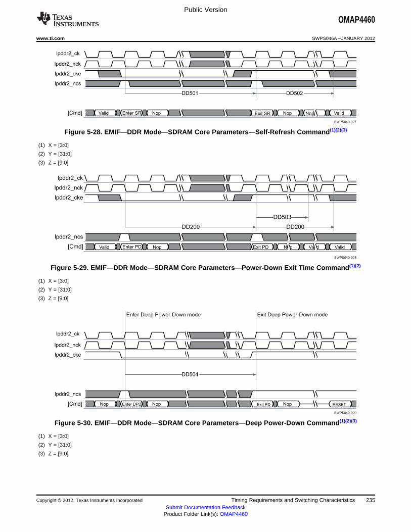
lpddr2_ck
lpddr2_nck
lpddr2_cke
lpddr2_ncs
[Cmd] Valid Enter SR Nop Exit SR Nop Nop Valid
DD501 DD502
SWPS040-027
lpddr2_ck
lpddr2_nck
lpddr2_cke
lpddr2_ncs
[Cmd] Valid Enter PD Nop Exit PD Nop Valid Valid
DD200DD200
DD503
SWPS040-028
lpddr2_ck
lpddr2_nck
lpddr2_cke
lpddr2_ncs
[Cmd] Nop Enter DPD Nop Exit PD Nop RESET
Enter Deep Power-Down mode Exit Deep Power-Down mode
DD504
SWPS040-029
Public Version
OMAP4460
www.ti.com SWPS046A –JANUARY 2012
Figure 5-28. EMIF—DDR Mode—SDRAM Core Parameters—Self-Refresh Command(1)(2)(3)
(1) X = [3:0]
(2) Y = [31:0]
(3) Z = [9:0]
Figure 5-29. EMIF—DDR Mode—SDRAM Core Parameters—Power-Down Exit Time Command(1)(2)
(1) X = [3:0]
(2) Y = [31:0]
(3) Z = [9:0]
Figure 5-30. EMIF—DDR Mode—SDRAM Core Parameters—Deep Power-Down Command(1)(2)(3)
(1) X = [3:0]
(2) Y = [31:0]
(3) Z = [9:0]
Copyright © 2012, Texas Instruments Incorporated Timing Requirements and Switching Characteristics 235Submit Documentation Feedback
Product Folder Link(s): OMAP4460
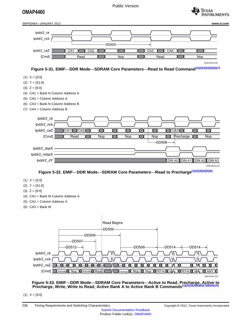
lpddr2_ck
lpddr2_nck
lpddr2_caZ
[Cmd]
CA1 CA2 CA3 CA4
Read Nop Read Nop
DD505
SWPS040-030
lpddr2_ck
lpddr2_nck
lpddr2_caZ
[Cmd]
lpddr2_dqsX
lpddr2_ndqsX
lpddr2_dY
CA1 CA2 CA3
Read Nop Nop Nop Precharge Nop
DIN A0 DIN A1 DIN A2 DIN A3
DD506
SWPS040-031
lpddr2_ck
lpddr2_nck
lpddr2_caZ
[Cmd]
CA1 CA2 CA3 CA4 CA5 CA6 CA7
Activate Nop Activate Read Precharge Nop Nop REFab Nop REFab Nop ANY
Read Begins
DD508
DD507
DD512
DD509
DD500
DD514 DD514
SWPS040-032
Public Version
OMAP4460
SWPS046A –JANUARY 2012 www.ti.com
Figure 5-31. EMIF—DDR Mode—SDRAM Core Parameters—Read to Read Command(1)(2)(3)(4)(5)(6)(7)
(1) X = [3:0]
(2) Y = [31:0]
(3) Z = [9:0]
(4) CA1 = Bank N Column Address A
(5) CA2 = Column Address A
(6) CA3 = Bank N Column Address B
(7) CA4 = Column Address B
Figure 5-32. EMIF—DDR Mode—SDRAM Core Parameters—Read to Precharge(1)(2)(3)(4)(5)(6)
(1) X = [3:0]
(2) Y = [31:0]
(3) Z = [9:0]
(4) CA1 = Bank M Column Address A
(5) CA2 = Column Address A
(6) CA3 = Bank M
Figure 5-33. EMIF—DDR Mode—SDRAM Core Parameters—Active to Read, Precharge, Active toPrecharge, Write, Write to Read, Active Bank A to Active Bank B Commands(1)(2)(3)(4)(5)(6)(7)(8)(9)(10)
(1) X = [3:0]
236 Timing Requirements and Switching Characteristics Copyright © 2012, Texas Instruments Incorporated
Submit Documentation FeedbackProduct Folder Link(s): OMAP4460

lpddr2_ck
lpddr2_nck
lpddr2_caZ
[Cmd]
lpddr2_dqsX
lpddr2_ndqsX
lpddr2_dY
CA1 CA2 CA3
Write Nop Nop Nop Nop Precharge Nop
DOUT A0 DOUT A1 DOUT A2 DOUT A3
Completion of Burst Write
DD510DD405_MAX
SWPS040-033
lpddr2_ck
lpddr2_nck
lpddr2_caZ
[Cmd]
lpddr2_dqsX
lpddr2_ndqsX
lpddr2_dZ
CA1 CA2 CA3 CA4
Write Nop Nop Nop Nop Nop Read
DOUT A0 DOUT A1 DOUT A2 DOUT A3
Completion of Burst Write
DD606
DD511
SWPS040-034
Public Version
OMAP4460
www.ti.com SWPS046A –JANUARY 2012
(2) Y = [31:0]
(3) Z = [9:0]
(4) CA1 = Bank A Row Address
(5) CA2 = Row Address
(6) CA3 = Bank B Row Address
(7) CA4 = Row Address
(8) CA5 = Bank A Column Address
(9) CA6 = Column Address
(10) CA7 = Bank A
Figure 5-34. EMIF—DDR Mode—SDRAM Core Parameters—Write Recovery Time(1)(2)(3)(4)(5)(6)
(1) X = [3:0]
(2) Y = [31:0]
(3) Z = [9:0]
(4) CA1 = Bank A Column Address A
(5) CA2 = Column Address
(6) CA3 = Bank A
Figure 5-35. EMIF—DDR Mode—SDRAM Core Parameters—Write to Read Command(1)(2)(3)(4)(5)(6)(7)(8)(9)(10)(11)
(1) X = [3:0]
(2) Y = [31:0]
(3) Z = [9:0]
(4) CA1[SDRAM DD511] = Bank M Column Address A
(5) CA2[SDRAM DD511] = Column Address A
Copyright © 2012, Texas Instruments Incorporated Timing Requirements and Switching Characteristics 237Submit Documentation Feedback
Product Folder Link(s): OMAP4460

lpddr2_ck
lpddr2_nck
lpddr2_caZ
[Cmd]
CA1 CA1 CA2 CA2 CA3 CA3 CA4 CA4 CA5 CA5
ACT Nop ACT Nop ACT Nop ACT Nop Nop Nop ACT Nop
DD512 DD512 DD512
DD513
SWPS040-035
lpddr2_ck
lpddr2_nck
lpddr2_caZ
[Cmd]
CA1 CA2 CA3 CA2 CA4 CA2 CA5 CA6 CA3 CA2 CA1 CA2
Preactive Nop Activate Nop Activate Read Nop Activate Nop Preactive
DD607 DD602
DD601
DD603
DD608
SWPS040-036
Public Version
OMAP4460
SWPS046A –JANUARY 2012 www.ti.com
(6) CA3[SDRAM DD511] = Bank N Column Address B
(7) CA4[SDRAM DD511] = Column Address B
(8) CA1[NVM DD606] = RDB M Column Address A
(9) CA2[NVM DD606] = Column Address A
(10) CA3[NVM DD606] = RDB N Column Address B
(11) CA4[NVM DD606] = Column Address B
Figure 5-36. EMIF—DDR Mode—SDRAM Core Parameters—Active to Active Command(1)(2)(3)(4)(5)(6)(7)(8)
(1) X = [3:0]
(2) Y = [31:0]
(3) Z = [9:0]
(4) CA1 = Bank A
(5) CA2 = Bank B
(6) CA3 = Bank C
(7) CA4 = Bank D
(8) CA5 = Bank E
Figure 5-37. EMIF—DDR Mode—NVM Core Parameters—Active to Read or Write, Active Bank A to ActiveBank B, Active to Active, Precharge to Active, Active to Preactive Commands(1)(2)(3)(4)(5)(6)(7)(8)(9)
(1) X = [3:0]
(2) Y = [31:0]
(3) Z = [9:0]
(4) CA1 = RAB A Row Address
(5) CA2 = Row Address
(6) CA3 = RB A Row Address
(7) CA4 = RB B Row Address
(8) CA5 = RDB A Column Address
(9) CA6 = Column Address
238 Timing Requirements and Switching Characteristics Copyright © 2012, Texas Instruments Incorporated
Submit Documentation FeedbackProduct Folder Link(s): OMAP4460

lpddr2_ck
lpddr2_nck
lpddr2_caZ
[Cmd]
lpddr2_dqsX
lpddr2_ndqsX
lpddr2_dY
CA1 CA2 CA3 CA4
Write Nop Nop Nop Nop Nop Activate
DOUT A0 DOUT A1 DOUT A2 DOUT A3
Completion of Burst Write
DD605
SWPS040-037
lpddr2_ck
lpddr2_nck
lpddr2_caZ
[Cmd]
lpddr2_dqsX
lpddr2_ndqsX
lpddr2_dY
CA1 CA2 CA3 CA4
Write Nop Write Nop
DOUT A0 DOUT A1 DOUT A2 DOUT A3
DD604
SWPS040-038
lpddr2_ck
lpddr2_nck
lpddr2_cke
lpddr2_ncs
[Cmd] Valid Enter PD Nop Exit PD Nop Valid Valid
DD609
SWPS040-039
Public Version
OMAP4460
www.ti.com SWPS046A –JANUARY 2012
Figure 5-38. EMIF—DDR Mode—NVM Core Parameters—Write Recovery Time Before Active(1)(2)(3)(4)(5)(6)(7)
(1) X = [3:0]
(2) Y = [31:0]
(3) Z = [9:0]
(4) CA1 = RDB A Column Address
(5) CA2 = Column Address
(6) CA3 = RB A Row Address
(7) CA4 = Row Address
Figure 5-39. EMIF—DDR Mode—NVM Core Parameters—CAS to CAS(1)(2)(3)(4)(5)(6)(7)
(1) X = [3:0]
(2) Y = [31:0]
(3) Z = [9:0]
(4) CA1 = RDB M Column Address A
(5) CA2 = Column Address A
(6) CA3 = RDB N Column Address B
(7) CA4 = Column Address B
Figure 5-40. EMIF—DDR Mode—NVM Core Parameters—Exit Power-Down to Next Valid Command(1)(2)(3)
Copyright © 2012, Texas Instruments Incorporated Timing Requirements and Switching Characteristics 239Submit Documentation Feedback
Product Folder Link(s): OMAP4460
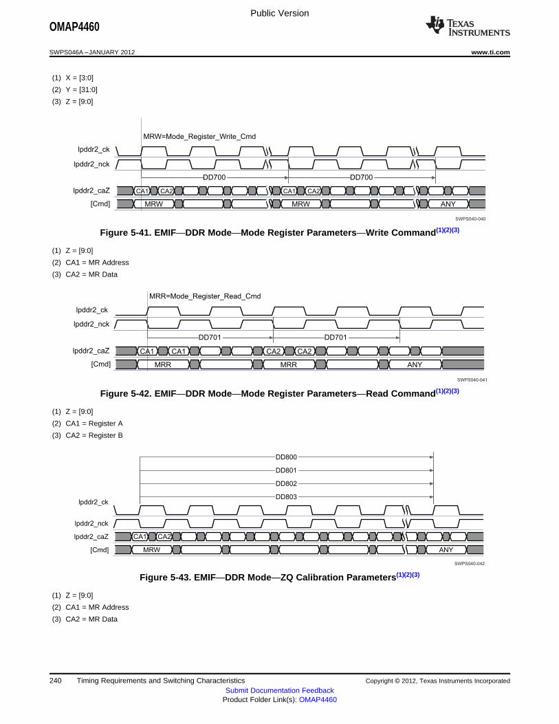
lpddr2_ck
lpddr2_nck
lpddr2_caZ
[Cmd]
CA1 CA2 CA1 CA2
MRW MRW ANY
MRW=Mode_Register_Write_Cmd
DD700 DD700
SWPS040-040
lpddr2_ck
lpddr2_nck
lpddr2_caZ
[Cmd]
CA1 CA1 CA2 CA2
MRR MRR ANY
MRR=Mode_Register_Read_Cmd
DD701 DD701
SWPS040-041
lpddr2_ck
lpddr2_nck
lpddr2_caZ
[Cmd]
CA1 CA2
MRW ANY
DD802
DD803
DD801
DD800
SWPS040-042
Public Version
OMAP4460
SWPS046A –JANUARY 2012 www.ti.com
(1) X = [3:0]
(2) Y = [31:0]
(3) Z = [9:0]
Figure 5-41. EMIF—DDR Mode—Mode Register Parameters—Write Command(1)(2)(3)
(1) Z = [9:0]
(2) CA1 = MR Address
(3) CA2 = MR Data
Figure 5-42. EMIF—DDR Mode—Mode Register Parameters—Read Command(1)(2)(3)
(1) Z = [9:0]
(2) CA1 = Register A
(3) CA2 = Register B
Figure 5-43. EMIF—DDR Mode—ZQ Calibration Parameters(1)(2)(3)
(1) Z = [9:0]
(2) CA1 = MR Address
(3) CA2 = MR Data
240 Timing Requirements and Switching Characteristics Copyright © 2012, Texas Instruments Incorporated
Submit Documentation FeedbackProduct Folder Link(s): OMAP4460
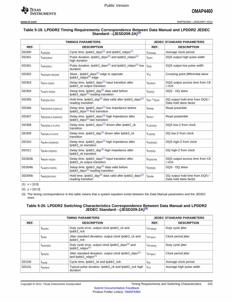
Public Version
OMAP4460
www.ti.com SWPS046A –JANUARY 2012
Table 5-19. LPDDR2 Timing Requirements Correspondence Between Data Manual and LPDDR2 JEDECStandard—(JESD209-2A)(3)
TIMINGS PARAMETERS JEDEC STANDARD PARAMETERS
REF. DESCRIPTION REF. DESCRIPTION
DD300 tc(DQSI) Cycle time, lpddr2_dqsx(1) and lpddr2_ndqsx(1) tCK(avg) Average clock period
DD301 tw(DQSIH) Pulse duration, lpddr2_dqsx(1) and lpddr2_ndqsx(1) tQSH DQS output high pulse widthhigh duration
DD301 tw(DQSIL) Pulse duration, lpddr2_dqsx(1) and lpddr2_ndqsx(1) low tQSL DQS output low pulse widthduration
DD302 tsk(DQSI-NDQSI) Skew , lpddr2_dqsx(1) edge to opposite VIX Crossing point differential skewlpddr2_ndqsx(1) edge
DD303 td(DV-DQSI) Delay time, lpddr2_dqsx(1) input transition after tDQSCK DQS output access time from CKlpddr2_ck output transition / nCK
DD304 tsu(DV-DQSI) Setup time, lpddr2_dqy(2) data valid before tDQSQ DQS - DQ skewlpddr2_dqsx(1) reading transition
DD305 th(DQSI-DIV) Hold time, lpddr2_dqy(2) data valid after lpddr2_dqsx(1) tQH / tQHS DQ output hold time from DQS /reading transition Data hold skew factor
DD306 td(DQSIHZ-DQSILZ) Delay time, lpddr2_dqsx(1) low impedance before tRPRE Read preamblelpddr2_dqsx(1) first transition
DD307 td(DQSILZ-DQSIHZ) Delay time, lpddr2_dqsx(1) high impedance after tRPST Read postamblelpddr2_dqsx(1) last transition
DD308 td(DQSILZ-CLKH) Delay time, lpddr2_dqsx(1) driven after lpddr2_ck tLZ(DQS) DQS low-Z from clocktransition
DD309 td(DQILZ-CLKH) Delay time, lpddr2_dqy(2) driven after lpddr2_ck tLZ(DQ) DQ low-Z from clocktransition
DD310 td(clkH-DQSIHZ) Delay time, lpddr2_dqsx(1) high impedance after tHZ(DQS) DQS high-Z from clocklpddr2_ck transition
DD311 td(clkH-DQIHZ) Delay time, lpddr2_dqy(2) high impedance after tHZ(DQ) DQ high-Z from clocklpddr2_ck transition
DD303b tdb(DV-DQSI) Delay time, lpddr2_dqsx(1) input transition after tDQSCKb DQS output access time from CKlpddr2_ck output transition / nCK
DD304b tsub(DV-DQSI) Setup time, lpddr2_dqy(2) data valid before tDQSQb DQS - DQ skewlpddr2_dqsx(1) reading transition
DD305b thb(DQSI-DIV) Hold time, lpddr2_dqy(2) data valid after lpddr2_dqsx(1) tQHSb DQ output hold time from DQS /reading transition Data hold skew factor
(1) x = [3:0]
(2) y = [31:0]
(3) The timing correspondence in this table means that a system equation exists between the Data Manual parameters and the JEDECones.
Table 5-20. LPDDR2 Switching Characteristics Correspondence Between Data Manual and LPDDR2JEDEC Standard—(JESD209-2A)(4)
TIMING PARAMETERS JEDEC STANDARD PARAMETERS
REF. DESCRIPTION REF. DESCRIPTION
tdc(clk) Duty cycle error, output clock lpddr2_ck and tJIT(duty) Duty cycle jitterlpddr2_nck
tj(clk) Jitter standard deviation, output clock lpddr2_ck and tJIT(per) Clock period jitterlpddr2_nck
tdc(DQS) Duty cycle error, output clock lpddr2_dqsx(1) and tJIT(duty) Duty cycle jitterlpddr2_ndqsx(1)
tj(DQS) Jitter standard deviation, output clock lpddr2_dqsx(1) tJIT(per) Clock period jitterand lpddr2_ndqsx(1)
DD100 tc(clk) Cycle time, lpddr2_ck and lpddr2_nck tCK Average clock period
DD101 tw(clkH) Typical pulse duration, lpddr2_ck and lpddr2_nck high tCH Average high pulse widthduration
Copyright © 2012, Texas Instruments Incorporated Timing Requirements and Switching Characteristics 241Submit Documentation Feedback
Product Folder Link(s): OMAP4460

Public Version
OMAP4460
SWPS046A –JANUARY 2012 www.ti.com
Table 5-20. LPDDR2 Switching Characteristics Correspondence Between Data Manual and LPDDR2JEDEC Standard—(JESD209-2A)(4) (continued)
TIMING PARAMETERS JEDEC STANDARD PARAMETERS
REF. DESCRIPTION REF. DESCRIPTION
DD101 tw(clkL) Typical pulse duration, lpddr2_ck and lpddr2_nck low tCL Average low pulse widthduration
DD102 tsk(clk-Nclk) Skew , lpddr2_ck edge to opposite lpddr2_nck edge VIX Crossing point differential skew
DD200 tw(CKE) Pulse duration, lpddr2_cke high and low duration tCKE CKE minimum pulse width (highand low pulse width)
DD201 td(clkL-CKE) Delay time, lpddr2_ck low to lpddr2_cke tIHCKE / CKE input setup / hold timetISCKE
DD202 td(clkL-NCS) Delay time, lpddr2_ck low to lpddr2_ncs tIH / tIS Address and control inputsetup/hold time
DD203 td(clk-CA) Delay time, lpddr2_ck low to lpddr2_caz(3) tIH / tIS Address and control inputsetup/hold time
DD204 tw(CA) Pulse duration, lpddr2_caz(3) high and low duration tIPW Adress and control input pulsewidth
DD200b tcb(clk) Cycle time, lpddr2_ck and lpddr2_nck tCKb Clock cycle time
DD201b tdb(clkL-CKE) Delay time, lpddr2_ck low to lpddr2_cke tISCKEb / CKE input setup/hold timetIHCKEb
DD202b tdb(clkL-NCS) Delay time, lpddr2_ck low to lpddr2_ncs tISb / tIHb Address and control input setup /hold time
DD203b tdb(clk-CA) Delay time, lpddr2_ck low to lpddr2_caz(3) tISb / tIHb Address and control input setup /hold time
DD400 tc(DQSO) Cycle time, lpddr2_dqsx(1) and lpddr2_ndqsx(1) tCK Clock period jitter
DD401 tw(DQSOH) Pulse duration, lpddr2_dqsx(1) and lpddr2_ndqsx(1) tDQSH DQS input high-level widthhigh duration
DD401 tw(DQSOL) Pulse duration, lpddr2_dqsx(1) and lpddr2_ndqsx(1) low tDQSL DQS input low-level widthduration
DD402 tsk(DQSO-NDQSO) Skew , lpddr2_dqsx(1) edge to opposite VIX Crossing point differential skewlpddr2_ndqsx(1) edge
DD403 td(DQSO-DQO/DM) Delay time, lpddr2_dqsx(1) to lpddr2_dqy(2) and tDS / tDH DQ and DM input setup/hold timelpddr2_dmx(1)
DD404 td(DV-DQSO) Delay time, lpddr2_dqsx(1) valid after lpddr2_ck tDSS / tDSH DQS falling edge to CK setup /transition hold time
DD405 td(clkV-DQSO) Delay time, lpddr2_ck valid to first lpddr2_dqsx(1) edge tDQSS Write command to first DQSlatching transition
DD406 td(DQSOHZ-DQSOV) Delay time, lpddr2_dqsx(1) high impedance to tWPRE Write pretamblelpddr2_dqsx(1) valid
DD407 td(DQSOV-DQSOHZ) Delay time, lpddr2_dqsx(1) last edge to lpddr2_dqsx(1) tWPST Write postamblehigh impedance state
DD408 tw(DQO/DM) Pulse duralion, lpddr2_dqy(2) and lpddr2_dmx(1) high / tDIPW DQ qnd DM output pulse widthlow duration
DD500 tc(ACT-ACT)s Cycle time, ACTIVE to ACTIVE command tRC ACTIVE to ACTIVE commandperiod
DD501 tw(SRL)s Pulse duralion, lpddr2_cke during SELF REFRESH tCKESR CKE MIN. pulse width duringlow duration self-refresh (low pulse width
during self-refresh)
DD502 tc(SR-VAL)s Cycle time, SELF REFRESH to VALID command tXSR Self refresh exit to next validcommand delay
DD503 td(DPWDN)s Delay time, POWER DOWN exit time tXP Exit power down to next validcommand delay
DD504 td(PWDN)s Delay time, DEEP POWER DOWN command tDPD MINimun deep power down time
DD505 tc(RD-RD)s Cycle time, READ to READ command tCCD LPDDR2-S4 CAS to CAS delay
DD506 tc(RD-PRE)s Cycle time, READ to PRECHARGE command tRTP Internal read to prechargecommand delay
DD507 tc(ACT-RD)s Cycle time, ACTIVE to READ command tRCD RAS to CAS delay
242 Timing Requirements and Switching Characteristics Copyright © 2012, Texas Instruments Incorporated
Submit Documentation FeedbackProduct Folder Link(s): OMAP4460

Public Version
OMAP4460
www.ti.com SWPS046A –JANUARY 2012
Table 5-20. LPDDR2 Switching Characteristics Correspondence Between Data Manual and LPDDR2JEDEC Standard—(JESD209-2A)(4) (continued)
TIMING PARAMETERS JEDEC STANDARD PARAMETERS
REF. DESCRIPTION REF. DESCRIPTION
DD508 td(PRE)s Delay time, PRECHARGE command (8-bank) tRPab (8-bank) Row precharge time (all banks)
DD509 tc(ACT-PRE)s Cycle time, ACTIVE to PRECHARGE command tRAS Row active time
DD510 td(WRREC)s Delay time, WRITE recovery time tWR Write recovery time
DD511 tc(WR-RD)s Cycle time, WRITE to READ command tWTR Internal write to read commanddelay
DD512 tc(ACTBA-ACTBB)s Cycle time, ACTIVE bank A to ACTIVE bank B tRRD Active bank A to active bank Bcommand
DD513 tc(ACT-4B-ACT)s Cycle time, four banks ACTIVE to ACTIVE command tFAW Four bank activate window
DD514 tc(REF)s Cycle time, four banks REFRESH Command tRFCab Refresh cycle time
DD601 tc(ACT-RD/WR)n Cycle time, ACTIVE to READ or WRITE command tRCD / Activate to read / write commandtRCDMIN period
DD602 tc(ACTBA-ACTBB)n Cycle time, ACTIVE bank A to ACTIVE bank B tRRD Activate to activate commandcommand period (different row buffer)
DD603 tc(ACT-ACT)n Cycle time, ACTIVE to ACTIVE command tRC Activate to activate commandperiod (same row buffer)
DD604 tc(CAS-CAS)n Cycle time, CAS to CAS command tCCD CAS to CAS delay
DD605 tc(WRREC-ACT)n Cycle time, WRITE recovery Time before ACTIVE tWRA Write recovery time beforeactivate
DD606 tc(WR-RD)n Cycle time, WRITE to READ command tWTR Internal write to read commanddelay
DD607 tc(PRE-ACT)n Cycle time, PRECHARGE to ACTIVE command tRP Preactive to activate commandperiod
DD608 tc(ACT-PRE)n Cycle time, ACTIVE to PREACTIVE command tRAS Activate to preactive commandperiod
DD609 tc(EXPWDN-VAL)n Cycle time, EXIT POWER DOWN to next valid tXP Exit power down to next validcommand command delay
DD700 td(MRW) Delay time, MODE REGISTER WRITE command tMRW MODE REGISTER writecommand period
DD701 td(MRR) Delay time, MODE REGISTER READ command tMRR MODE REGISTER readcommand period
DD800 td(QINIT) Delay time, initialization calibration command tZQINIT Initialization calibration time
DD801 td(QCL) Delay time, long calibration command tZQCL Long calibration time
DD802 td(QCS) Delay time, short calibration command tZQCS Short calibration time
DD803 td(QRESET) Delay time, calibration reset command tZQRESET Calibration reset time
(1) x = [3:0]
(2) y = [31:0]
(3) z = [9:0]
(4) The timing correspondence in this table means that a system equation exists between the Data Manual parameters and the JEDECones.
5.5 Multimedia Interfaces
5.5.1 Camera Interface
The camera subsystem supports most of the raw image sensors available in the market. It contains twoserial interfaces compatible with the CCP, MIPI® CSI1, and CSI2 protocols.
The main serial interface, CSI21, supports up to 4 data lanes (824 Mb/s maximum with 4 data lanes (412MHz), 1Gb/s maximum with 3, 2, or 1 data lane(s) (500 MHz)) using CSI2 MIPI® standard.
The secondary CSI22 interface provides both CSI2 and CCP2 / CSI1 modes:• CSI2 at 500 MHz (1 Gbps) in double data rate (DDR) mode
Copyright © 2012, Texas Instruments Incorporated Timing Requirements and Switching Characteristics 243Submit Documentation Feedback
Product Folder Link(s): OMAP4460
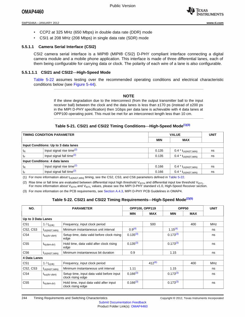
Public Version
OMAP4460
SWPS046A –JANUARY 2012 www.ti.com
• CCP2 at 325 MHz (650 Mbps) in double data rate (DDR) mode• CSI1 at 208 MHz (208 Mbps) in single data rate (SDR) mode
5.5.1.1 Camera Serial Interface (CSI2)
CSI2 camera serial interface is a MIPI® (MIPI® CSI2) D-PHY compliant interface connecting a digitalcamera module and a mobile phone application. This interface is made of three differential lanes, each ofthem being configurable for carrying data or clock. The polarity of each wire of a lane is also configurable.
5.5.1.1.1 CSI21 and CSI22—High-Speed Mode
Table 5-22 assumes testing over the recommended operating conditions and electrical characteristicconditions below (see Figure 5-44).
NOTEIf the skew degradation due to the interconnect (from the output transmitter ball to the inputreceiver ball) between the clock and the data lanes is less than ±170 ps (instead of ±200 psin the MIPI D-PHY specification) then 1Gbps per data lane is achievable with 4 data lanes atOPP100 operating point. This must be met for an interconnect length less than 10 cm.
Table 5-21. CSI21 and CSI22 Timing Conditions—High-Speed Mode(1)(3)
TIMING CONDITION PARAMETER VALUE UNIT
MIN MAX
Input Conditions: Up to 3 data lanes
tR Input signal rise time(2) 0.135 0.4 * tUI(INST,MIN) ns
tF Input signal fall time(2) 0.135 0.4 * tUI(INST,MIN) ns
Input Conditions: 4 data lanes
tR Input signal rise time(2) 0.166 0.4 * tUI(INST,MIN) ns
tF Input signal fall time(2) 0.166 0.4 * tUI(INST,MIN) ns
(1) For more information about tUI(INST,MIN) timing, see the CS2, CS3, and CS6 parameters defined in Table 5-22.
(2) Rise time or fall time are evaluated between differential input high threshold VIDTH and differential input low threshold VIDTL.For more information about VIDTH and VIDTL values, please see the MIPI D-PHY standard v1.0, High-Speed Receiver section.
(3) For more information on the PCB requirements, see Section A.4.3, MIPI D-PHY PCB Guidelines in OMAP4.
Table 5-22. CSI21 and CSI22 Timing Requirements—High-Speed Mode(2)(5)
NO. PARAMETER OPP100, OPP119 OPP50 UNIT
MIN MAX MIN MAX
Up to 3 Data Lanes
CS1 1 / tc(clk) Frequency, input clock period 500 400 MHz
CS2, CS3 tUI(INST,MIN) Minimum instantaneous unit interval 0.9(4) 1.15(4) ns
CS4 tsu(dV-clkH) Setup time, data valid before clock rising 0.135(3) 0.173(3) nsedge
CS5 th(clkH-dV) Hold time, data valid after clock rising 0.135(3) 0.173(3) nsedge
CS6 tUI(INST,MIN) Minimum instantaneous bit duration 0.9 1.15 ns
4 Data Lanes
CS1 1 / tc(clk) Frequency, input clock period 412(6) 400 MHz
CS2, CS3 tUI(INST,MIN) Minimum instantaneous unit interval 1.11 1.15 ns
CS4 tsu(dV-clkH) Setup time, input data valid before input 0.166(3) 0.173(3) nsclock rising edge
CS5 th(clkH-dV) Hold time, input data valid after input 0.166(3) 0.173(3) nsclock rising edge
244 Timing Requirements and Switching Characteristics Copyright © 2012, Texas Instruments Incorporated
Submit Documentation FeedbackProduct Folder Link(s): OMAP4460

csi2_dwn
csi2_dwn
csi2_dwn
Data (j-1)Data (j-1) Data_j Data_(j+1)
Data_(k-1)Data_(k-1) Data_k Data_(k+1)
CS4
CS4
CS5
CS5
CS1
CS3 CS2
CS6
CS6
SWPS040-043
Public Version
OMAP4460
www.ti.com SWPS046A –JANUARY 2012
Table 5-22. CSI21 and CSI22 Timing Requirements—High-Speed Mode(2)(5) (continued)
NO. PARAMETER OPP100, OPP119 OPP50 UNIT
MIN MAX MIN MAX
CS6 tUI(INST,MIN) Minimum instantaneous bit duration 1.11 1.15 ns
(1) Related to the input maximum frequency supported by the CSI21 and CSI22 modules.
(2) The timing requirements are assured up to the minimum instantaneous bit duration.
(3) Setup/hold time = 0.15 x tUI(INST,MIN)
(4) tUI(INST,MIN) = tUI(NOM) – 100 psWhere: tUI(NOM) is the minimum unit interval. tUI(NOM) = 0.5 * tc(clk).
(5) See DM Operating Condition Addendum for CORE OPP voltages.
(6) If the skew degradation due to the interconnect (from the output transmitter ball to the input receiver ball) between the clock and thedata lanes is less than ±170 ps (instead of ±200 ps in the MIPI D-PHY specification) then 1Gbps per data lane is achievable with 4 datalanes at OPP100 operating point. This must be met for an interconnect length less than 10 cm.
Figure 5-44. CSI21 and CSI22—High-Speed Mode(1)(2)(3)
(1) In csi2z_dwn, w is equal to x or y, n is equal to 0, 1, 2, 3, or 4 and z is equal to 1 or 2.
(2) The use of each csi2z_dwn lane (clock or data) is software programmable with the CSI2[1 or 2]_COMPLEXIO_CFG1 register, by settingbits field CLOCK_POSITION to 0x1, 0x2, 0x3, 0x4, 0x5.
(3) The polarity of each csi2z_dwn lane is software programmable with the CSI2[1 or 2]_COMPLEXIO_CFG1 register, DATAi_POL bit field.
5.5.1.1.2 CSI21 and CSI22—Low-Power and Ultralow-Power Modes
Table 5-24 assumes testing over the recommended operating conditions and electrical characteristicconditions below (see Figure 5-45).
Table 5-23. CSI21 and CSI22 Timing Conditions—Low-Power and Ultralow-Power Modes(2)
TIMING CONDITION PARAMETER VALUE UNIT
MIN MAX
Input Conditions
tR Input signal rise time(1) 2.6 25 ns
tF Input signal fall time(1) 2.6 25 ns
(1) Rise or fall time between 15% and 85% of the full signal swing. Input rise and fall times (tR and tF) are not applicable for clock lane.
(2) For more information on the PCB requirements, see Section A.4.3, MIPI D-PHY PCB Guidelines in OMAP4.
Table 5-24. CSI21 and CSI22 Timing Requirements—Low-Power and Ultralow-Power Modes(2)
NO. PARAMETER OPP100, OPP119 OPP50 UNIT
MIN MAX MIN MAX
CS7 tV(LPstate) Duration of a low-power state(1) 20 20 ns
tc(xorclk) Period of the LP exclusive-OR clock 90 90 ns
Copyright © 2012, Texas Instruments Incorporated Timing Requirements and Switching Characteristics 245Submit Documentation Feedback
Product Folder Link(s): OMAP4460
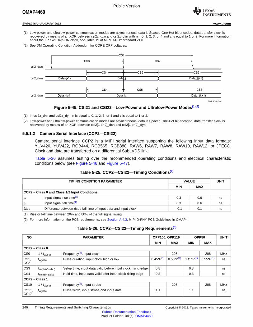
csi2_dwn
csi2_dwn
csi2_dwn
Data (j-1)Data (j-1) Data_j Data_(j+1)
Data_(k-1)Data_(k-1) Data_k Data_(k+1)
CS4
CS4
CS5
CS5
CS1
CS3 CS2
CS6
CS6
SWPS040-044
Public Version
OMAP4460
SWPS046A –JANUARY 2012 www.ti.com
(1) Low-power and ultralow-power communication modes are asynchronous, data is Spaced-One-Hot bit encoded, data transfer clock isrecovered by means of an XOR between csi2z_dxn and csi2z_dyn with n = 0, 1, 2, 3, or 4 and z is equal to 1 or 2. For more informationabout the LP exclusive-OR clock, see Table 19 of MIPI D-PHY standard v1.0.
(2) See DM Operating Condition Addendum for CORE OPP voltages.
Figure 5-45. CSI21 and CSI22—Low-Power and Ultralow-Power Modes(1)(2)
(1) In csi2z_dxn and csi2z_dyn, n is equal to 0, 1, 2, 3, or 4 and z is equal to 1 or 2.
(2) Low-power and ultralow-power communication modes are asynchronous, data is Spaced-One-Hot bit encoded, data transfer clock isrecovered by means of an XOR between csi2[1 or 2]_dxn and csi2[1 or 2]_dyn.
5.5.1.2 Camera Serial Interface (CCP2—CSI22)
Camera serial interface CCP2 is a MIPI serial interface supporting the following input data formats:YUV420, YUV422, RGB444, RGB565, RGB888, RAW6, RAW7, RAW8, RAW10, RAW12, or JPEG8.Clock and data are transferred on a differential SubLVDS link.
Table 5-26 assumes testing over the recommended operating conditions and electrical characteristicconditions below (see Figure 5-46 and Figure 5-47).
Table 5-25. CCP2—CSI22—Timing Conditions(2)
TIMING CONDITION PARAMETER VALUE UNIT
MIN MAX
CCP2 – Class 0 and Class 1/2 Input Conditions
tR Input signal rise time(1) 0.3 0.6 ns
tF Input signal fall time(1) 0.3 0.6 ns
ΔtRF Difference between rise / fall time of input data and input clock –0.1 0.1 ns
(1) Rise or fall time between 20% and 80% of the full signal swing.
(2) For more information on the PCB requirements, see Section A.4.3, MIPI D-PHY PCB Guidelines in OMAP4.
Table 5-26. CCP2—CSI22—Timing Requirements(3)
NO. PARAMETER OPP100, OPP119 OPP50 UNIT
MIN MAX MIN MAX
CCP2 – Class 0
CS0 1 / tc(strb) Frequency(2), input clock 208 208 MHz
CS1, tw(strb) Pulse duration, input clock high or low 0.45*P(1) 0.55*P(1) 0.45*P(1) 0.55*P(1) nsCS2
CS3 tsu(datV-strbH) Setup time, input data valid before input clock rising edge 0.8 0.8 ns
CS4 th(strbH-datV) Hold time, input data valid after input clock rising edge 0.8 0.8 ns
CCP2 – Class 1
CS10 1 / tc(strb) Frequency(2), input strobe 208 208 MHz
CS11, tw(strb) Pulse width, input strobe and input data 1.1 1.1 nsCS17
246 Timing Requirements and Switching Characteristics Copyright © 2012, Texas Instruments Incorporated
Submit Documentation FeedbackProduct Folder Link(s): OMAP4460

CS12 CS13
ccpv2_dx0.ccpv2_dy0
ccpv2_dx1.ccpv2_dy1
SWPS040-045
CS0 CS1 CS2
CS10CS11
CS12 CS13
ccpv2_dx0.ccpv2_dy0
ccpv2_dx1.ccpv2_dy1
SWPS040-046
Public Version
OMAP4460
www.ti.com SWPS046A –JANUARY 2012
Table 5-26. CCP2—CSI22—Timing Requirements(3) (continued)
NO. PARAMETER OPP100, OPP119 OPP50 UNIT
MIN MAX MIN MAX
CS12 tsk(datV-strbH) Skew time, input data valid before input strobe rising 0.78 0.78 nsedge
CS13 tsk(strbH-datV) Skew time, input data valid after input strobe falling edge 0.78 0.78 ns
CCP2 – Class 2
CS10 1 / tc(strb) Frequency(2), input strobe 325 325 MHz
CS11, tw(strb) Pulse width, input strobe and input data 1.1 1.1 nsCS17
CS12 tsk(datV-strbH) Skew time, input data valid before input strobe rising 0.78 0.78 nsedge
CS13 tsk(strbH-datV) Skew time, input data valid after input strobe falling edge 0.78 0.78 ns
(1) P = clock period in ns
(2) The maximum clock frequency of the CCP2 must be chosen to be the lowest possible for the application / transmitting device to reducethe power consumption of the sensor, the IO pad of the device and the camera core module itself.
(3) See DM Operating Condition Addendum for CORE OPP voltages.
Figure 5-46. CCP2—CSI22—Class 0(1)(2)(3)
(1) ccpv2_dx0/ccpv2_dy0 and ccpv2_dx1/ccpv2_dy1 are the result of low-voltage differential data signal converters (see the CameraSubsystem in OMAP4460 TRM).
(2) The CCP2 receives up to 208 Mbps data rate or data/clock transmission.
(3) The CCP2 supports YUV422, YUV420, Bayer RGB444, RGB565, RGB888, RAW Bayer 6-, 7-, 8-, 10-, and 12-bit, and JPEG8 input dataformats.
Figure 5-47. CCP2—CSI22—Class 1, Class 2(1)(2)(3)
(1) ccpv2_dx0/ccpv2_dy0 and ccpv2_dx1/ccpv2_dy1 are the result of low-voltage differential data signal converters (see the CameraSubsystem in OMAP4460 TRM).
(2) The CCP2 receives up to 208 Mbps data rate or data/clock transmission and up to 416 or 650 Mbps data rate for data/strobetransmission.
(3) The CCP2 supports YUV422, YUV420, Bayer RGB444, RGB565, RGB888, RAW Bayer 6-, 7-, 8-, 10-, and 12-bit, and JPEG8 input dataformats.
Copyright © 2012, Texas Instruments Incorporated Timing Requirements and Switching Characteristics 247Submit Documentation Feedback
Product Folder Link(s): OMAP4460
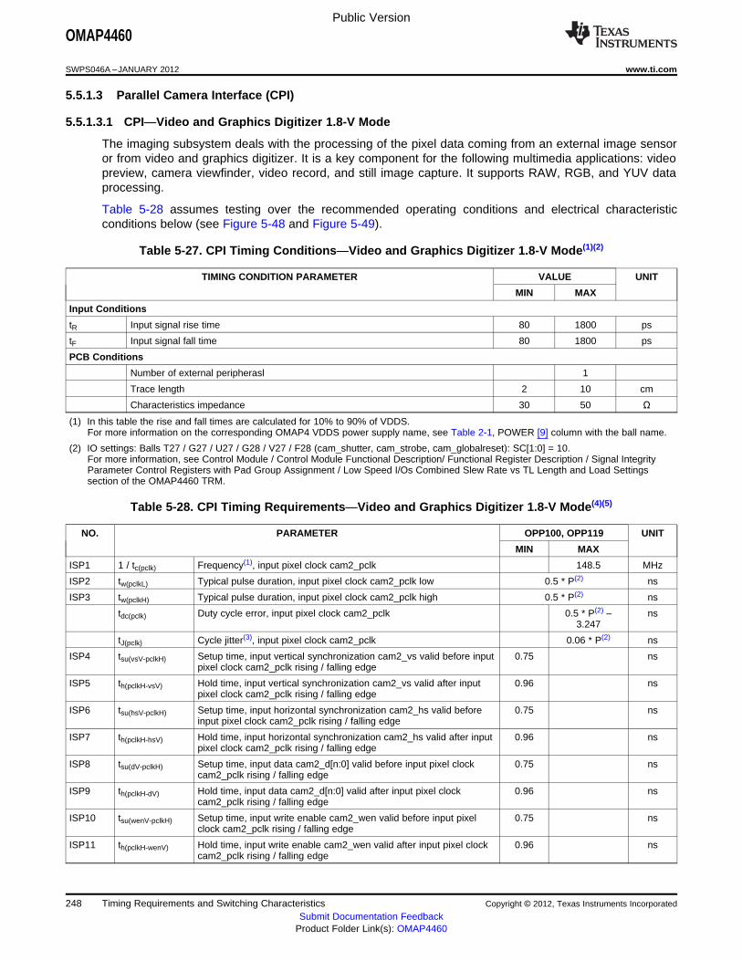
Public Version
OMAP4460
SWPS046A –JANUARY 2012 www.ti.com
5.5.1.3 Parallel Camera Interface (CPI)
5.5.1.3.1 CPI—Video and Graphics Digitizer 1.8-V Mode
The imaging subsystem deals with the processing of the pixel data coming from an external image sensoror from video and graphics digitizer. It is a key component for the following multimedia applications: videopreview, camera viewfinder, video record, and still image capture. It supports RAW, RGB, and YUV dataprocessing.
Table 5-28 assumes testing over the recommended operating conditions and electrical characteristicconditions below (see Figure 5-48 and Figure 5-49).
Table 5-27. CPI Timing Conditions—Video and Graphics Digitizer 1.8-V Mode(1)(2)
TIMING CONDITION PARAMETER VALUE UNIT
MIN MAX
Input Conditions
tR Input signal rise time 80 1800 ps
tF Input signal fall time 80 1800 ps
PCB Conditions
Number of external peripherasl 1
Trace length 2 10 cm
Characteristics impedance 30 50 Ω
(1) In this table the rise and fall times are calculated for 10% to 90% of VDDS.For more information on the corresponding OMAP4 VDDS power supply name, see Table 2-1, POWER [9] column with the ball name.
(2) IO settings: Balls T27 / G27 / U27 / G28 / V27 / F28 (cam_shutter, cam_strobe, cam_globalreset): SC[1:0] = 10.For more information, see Control Module / Control Module Functional Description/ Functional Register Description / Signal IntegrityParameter Control Registers with Pad Group Assignment / Low Speed I/Os Combined Slew Rate vs TL Length and Load Settingssection of the OMAP4460 TRM.
Table 5-28. CPI Timing Requirements—Video and Graphics Digitizer 1.8-V Mode(4)(5)
NO. PARAMETER OPP100, OPP119 UNIT
MIN MAX
ISP1 1 / tc(pclk) Frequency(1), input pixel clock cam2_pclk 148.5 MHz
ISP2 tw(pclkL) Typical pulse duration, input pixel clock cam2_pclk low 0.5 * P(2) ns
ISP3 tw(pclkH) Typical pulse duration, input pixel clock cam2_pclk high 0.5 * P(2) ns
tdc(pclk) Duty cycle error, input pixel clock cam2_pclk 0.5 * P(2) – ns3.247
tJ(pclk) Cycle jitter(3), input pixel clock cam2_pclk 0.06 * P(2) ns
ISP4 tsu(vsV-pclkH) Setup time, input vertical synchronization cam2_vs valid before input 0.75 nspixel clock cam2_pclk rising / falling edge
ISP5 th(pclkH-vsV) Hold time, input vertical synchronization cam2_vs valid after input 0.96 nspixel clock cam2_pclk rising / falling edge
ISP6 tsu(hsV-pclkH) Setup time, input horizontal synchronization cam2_hs valid before 0.75 nsinput pixel clock cam2_pclk rising / falling edge
ISP7 th(pclkH-hsV) Hold time, input horizontal synchronization cam2_hs valid after input 0.96 nspixel clock cam2_pclk rising / falling edge
ISP8 tsu(dV-pclkH) Setup time, input data cam2_d[n:0] valid before input pixel clock 0.75 nscam2_pclk rising / falling edge
ISP9 th(pclkH-dV) Hold time, input data cam2_d[n:0] valid after input pixel clock 0.96 nscam2_pclk rising / falling edge
ISP10 tsu(wenV-pclkH) Setup time, input write enable cam2_wen valid before input pixel 0.75 nsclock cam2_pclk rising / falling edge
ISP11 th(pclkH-wenV) Hold time, input write enable cam2_wen valid after input pixel clock 0.96 nscam2_pclk rising / falling edge
248 Timing Requirements and Switching Characteristics Copyright © 2012, Texas Instruments Incorporated
Submit Documentation FeedbackProduct Folder Link(s): OMAP4460

D(n-2)
cam2_pclk
cam2_vs
cam2_hs
cam2_d[N:0]
cam2_wen
cam2_fld
D(0) D(n-2) D(n-1) D(0) D(n-1)
ISP1
ISP4 ISP5
ISP6 ISP7
ISP9
ISP8
ISP10 ISP11
ISP3
SWPS038-048
ISP2
Public Version
OMAP4460
www.ti.com SWPS046A –JANUARY 2012
Table 5-28. CPI Timing Requirements—Video and Graphics Digitizer 1.8-V Mode(4)(5) (continued)
NO. PARAMETER OPP100, OPP119 UNIT
MIN MAX
ISP12 tsu(fldV-pclkH) Setup time, input field identification cam2_fld valid before input pixel 0.75 nsclock cam2_pclk rising / falling edge
ISP13 th(pclkH-fldV) Hold time, input field identification cam2_fld valid after input pixel 0.96 nsclock cam2_pclk rising / falling edge
(1) Related with the input maximum frequency supported by the ISP module in 8-bit mode with 8 to 16 data bits conversion bridge enabled.
(2) P = cam2_pclk period in ns
(3) Maximum cycle jitter supported by cam2_pclk input clock.
(4) The timing requirements are assured for the cycle jitter and duty cycle error conditions specified.
(5) See DM Operating Condition Addendum for OPP voltages.
Figure 5-48. CPI—Video and Graphics Digitizer—1.8-V Progressive Mode(1)
(1) The polarity of cam2_pclk, cam2_fld, cam2_vs, and cam2_hs are software configurable. Optionally, the cam2_wen signal can be usedas an external memory write-enable signal. For further details, see the OMAP4460 TRM.
Copyright © 2012, Texas Instruments Incorporated Timing Requirements and Switching Characteristics 249Submit Documentation Feedback
Product Folder Link(s): OMAP4460

cam2_pclk
cam2_vs
cam2_hs
cam2_d[N:0]
cam2_wen
cam2_fld
D(n–1) D(0) D(n–1) D(0) D(n–1)
EVEN ODD
ISP1 ISP2
ISP4 ISP5
ISP6 ISP7
ISP9
ISP8
ISP10 ISP11
ISP3
ISP12 ISP13
SWPS038-049
D(0) D(0) D(n–1)
Public Version
OMAP4460
SWPS046A –JANUARY 2012 www.ti.com
Figure 5-49. CPI—Video and Graphics Digitizer—1.8-V Interlaced Mode(1)
(1) The polarity of cam2_pclk, cam2_fld, cam2_vs, and cam2_hs are software configurable. Optionally, the cam2_wen signal can be usedas an external memory write-enable signal. For further details, see the OMAP4460 TRM.
250 Timing Requirements and Switching Characteristics Copyright © 2012, Texas Instruments Incorporated
Submit Documentation FeedbackProduct Folder Link(s): OMAP4460
Public Version
OMAP4460
www.ti.com SWPS046A –JANUARY 2012
5.5.2 Display Subsystem Interface
NOTEFor more information, see the Display Subsystem chapter in the OMAP4460 TRM.
The display subsystem (DSS) provides the logic to display a video frame from the memory frame buffer ona liquid-crystal display (LCD) panel or a TV set. The modules integrated in the display subsystem are:• Display controller (DISPC)• Remote Frame Buffer Interface (RFBI)• Display Serial Interface (DSI)• NTSC/PAL video encoder (VENC)
NOTEThe NTSC/PAL video encoder (VENC) is not described in the OMAP4460 Data Manual.
• High Definition Multimedia Interface (HDMI)
5.5.2.1 DSS—Display Controller (DISPC)
The DISPC interface consists of:• 24-bit data bus• Horizontal synchronization signal (HSYNC)• Vertical synchronization signal (VSYNC)• Data enable (DE)• Pixel clock (PCLK)
This interface is functionally compliant to MIPI DPI standard revision 1.0 and delivers the parallel pixel /synchronization signals of the secondary LCD pipeline. DSI1 output must be deactivating when DISPC2port is used.
5.5.2.1.1 DSS—DISPC—Quad eXtended Graphics Array (QXGA) Application—SDR Mode
Table 5-30 assumes testing over the recommended operating conditions and electrical characteristicconditions below (see Figure 5-50).
Table 5-29. DISPC Timing Conditions—QXGA SDR Mode(1)(2)(4)
TIMING CONDITION PARAMETER VALUE UNIT
MIN MAX
PCB Conditions(3)
Number of external peripherals 1
Far end load 5 pF
Trace length 2 cm
Characteristics impedance 30 50 Ω
(1) IO settings: DS0 = 1.For more information, see Control Module / Control Module Functional Description/ Functional Register Description / Signal IntegrityParameter Control Registers with Pad Group Assignment / I/O cells with Configurable Output Driver Impedance section of theOMAP4460 TRM.
(2) In this table the rise and fall times are calculated for 10% to 90% of VDDS. For more information on the corresponding OMAP4 VDDSpower supply name, see Table 2-1, POWER [9] column with the ball name.
(3) Minimize the number of vias by layer transitions.
(4) To have an idea of the output OMAP4 ball load supported for this application, you can consider the following:Output OMAP4 ball load = Far End load + 1.34 pF/cm typical x trace length (cm).
Copyright © 2012, Texas Instruments Incorporated Timing Requirements and Switching Characteristics 251Submit Documentation Feedback
Product Folder Link(s): OMAP4460

Public Version
OMAP4460
SWPS046A –JANUARY 2012 www.ti.com
Table 5-30. DISPC Switching Characteristics—QXGA SDR Mode(4)
NO. PARAMETER OPP100, OPP119 UNIT
MIN MAX
D1 1 / tc(pclk) Frequency(1), output pixel clock dispc2_pclk 170 MHz
D2 tw(pclkL) Pulse duration, output pixel clock dispc2_pclk low 0.5*P(2) ns
D3 tw(pclkH) Pulse duration, output pixel clock dispc2_pclk high 0.5*P(2) ns
tdc(pclk) Duty cycle error, output pixel clock dispc2_pclk –118 118 ps
tj(pclk) Jitter standard deviation(3), output pixel clock dispc2_pclk 39 ps
tR(pclk) Rise time, output pixel clock dispc2_pclk 1066 ps
tF(pclk) Fall time, output pixel clock dispc2_pclk 959 ps
D4 td(pclkA- Delay time, output pixel clock dispc2_pclk transition to output vertical –1832 332 psvsyncV) synchronization dispc2_vsync valid
tR(vsync) Rise time, output vertical synchronization dispc2_vsync 1066 ps
tF(vsync) Fall time, output vertical synchronization dispc2_vsync 959 ps
D5 td(pclkA- Delay time, output pixel clock dispc2_pclk transition to output –1832 332 pshsyncV) horizontal synchronization dispc2_hsync valid
tR(hsync) Rise time, output horizontal synchronization dispc2_hsync 1066 ps
tF(hsync) Fall time, output horizontal synchronization dispc2_hsync 959 ps
D6 td(pclkA-dV) Delay time, output pixel clock dispc2_pclk transition to output data –1832 332 psdispc2_data[23:0] valid
tR(d) Rise time, output data dispc2_data[23:0] 1066 ps
tF(d) Fall time, output data dispc2_data[23:0] 959 ps
D7 td(pclkA-deV) Delay time, output pixel clock dispc2_pclk transition to output data –1832 332 psenable dispc2_de valid
tR(de) Rise time, output data enable dispc2_de 1066 ps
tF(de) Fall time, output data enable dispc2_de 959 ps
D8 td(pclkA-fidV) Delay time, output pixel clock dispc2_pclk transition to output field ID –1832 332 psdispc2_fid valid
tR(fid) Rise time, output field ID dispc2_fid 1066 ps
tF(fid) Fall time, output field ID dispc2_fid 959 ps
(1) Related to the output dispc2_clk(4) maximum frequency programmable.
(2) P = output dispc2_pclk period in ns
(3) The jitter probability density can be approximated by a Gaussian function.
(4) See DM Operating Condition Addendum for CORE OPP voltages.
252 Timing Requirements and Switching Characteristics Copyright © 2012, Texas Instruments Incorporated
Submit Documentation FeedbackProduct Folder Link(s): OMAP4460

dispcx_pclk
dispcx_vsync
dispcx_hsync
dispcx_data[23:0]
dispcx_de
dispcx_fid
data_1 data_2 data_n
odd even
D1
D2
D3
D4 D4
D5
D5
D6
D7
D8
D7
SWPS040-047
Public Version
OMAP4460
www.ti.com SWPS046A –JANUARY 2012
Figure 5-50. DSS—DISPC—QXGA SDR Application(1)(2)(3)(4)(5)(6)
(1) The configuration of assertion of the data can be programmed on the falling edge or rising edge of the pixel clock.
(2) In progressive mode, dispcx_fid signal is set to 0. In interlaced mode, the dispcx_fid signal toggles on the back edge of the verticalpulse.
(3) The polarity and the pulse width of dispcx_hsync and dispcx_vsync are programmable; see the DSS chapter in the OMAP4460 TRM.
(4) The dispcx_pclk(5) frequency can be configured, see DSS chapter in the OMAP4460 TRM.
(5) In dispcx_clk, x = 2
(6) For more information, see the DISPC chapter in the OMAP4460 TRM.
Copyright © 2012, Texas Instruments Incorporated Timing Requirements and Switching Characteristics 253Submit Documentation Feedback
Product Folder Link(s): OMAP4460
Public Version
OMAP4460
SWPS046A –JANUARY 2012 www.ti.com
5.5.2.2 DSS—Remote Frame Buffer Interface (RFBI) Applications
5.5.2.2.1 DSS—Remote Frame Buffer Interface (RFBI)—MIPI DBI2.0—LCD Panel
NOTEFor more information, see the Remote Frame Buffer Interface chapter in the OMAP4460TRM.
The remote frame buffer interface (RFBI) module is part of the display subsystem that provides the logic todisplay a picture from the memory frame buffer (SDRAM or SRAM) on a liquid-crystal display (LCD) panel.
Table 5-32 and Table 5-33 assume testing over the recommended operating conditions and electricalcharacteristic conditions below (see Figure 5-51 through Figure 5-53).
Table 5-31. DSS—RFBI Timing Conditions—LCD Panel(1)(2)(3)
TIMING CONDITION PARAMETER VALUE UNIT
MIN MAX
Input Conditions
tR Input signal rise time 15 ns
tF Input signal fall time 15 ns
PCB Conditions
Number of external peripherals 1
Far end load 30 pF
Trace length 20 cm
Characteristics impedance 20 50 Ω
(1) IO settings: DS0 = 0.For more information, see Control Module / Control Module Functional Description / Functional Register Description / Signal IntegrityParameter Control Registers with Pad Group Assignment / I/O cells with Configurable Output Driver Impedance section of theOMAP4460 TRM.
(2) In this table the rise and fall times are calculated for 30% to 70% of VDDS. For more information on the corresponding OMAP4 VDDSpower supply name, see Table 2-1, POWER [9] column with the ball name.
(3) To have an idea of the output OMAP4 ball load supported for this application, you can consider the following:Output OMAP4 ball load = Far End load + 1.34 pF/cm typical x trace length (cm).
Table 5-32. DSS—RFBI Timing Requirements—LCD Panel
NO. PARAMETER OPP100, OPP119 OPP50 UNIT
MIN MAX MIN MAX
DR0 tsu(dataV-rfbi_rdH) Setup time, rfbi_data[n:0](2) valid to rfbi_rd 20 20 nshigh
DR1 th(rfbi_rdH-dataIV) Hold time, rfbi_rd high to rfbi_data[n:0](2) 5.6 5.6 nsinvalid
td(Data sampled) rfbi_data are sampled at the end of the access N(1) N(1) nstime
(1) N = (AccessTime) * (TimeParaGranularity + 1) * L3CLK
(2) rfbi_data[n:0], n up to 8
Table 5-33. DSS—RFBI Switching Characteristics—LCD Panel
NO. PARAMETER OPP100, OPP119 OPP50 UNIT
MIN MAX MIN MAX
tw(rfbi_wrH) Pulse duration, rfbi_we high A(1) A(1) ns
tw(rfbi_wrL) Pulse duration, rfbi_we low B(2) B(2) ns
td(rfbi_a0-rfbi_wrL) Delay time, rfbi_a0 transition to rfbi_we low C(3) C(3) ns
254 Timing Requirements and Switching Characteristics Copyright © 2012, Texas Instruments Incorporated
Submit Documentation FeedbackProduct Folder Link(s): OMAP4460

Public Version
OMAP4460
www.ti.com SWPS046A –JANUARY 2012
Table 5-33. DSS—RFBI Switching Characteristics—LCD Panel (continued)
NO. PARAMETER OPP100, OPP119 OPP50 UNIT
MIN MAX MIN MAX
td(rfbi_wrH-rfbi_a0) Delay time, rfbi_we high to rfbi_a0 transition D(4) D(4) ns
td(rfbi_csx-rfbi_wrL) Delay time, rfbi_csx(14) low to rfbi_we low E(5) E(5) ns
td(rfbi_wrH- Delay time, rfbi_we high to rfbi_csx(14) high F(6) F(6) nsrfbi_csxH)
td(dataV) Output rfbi_data[n:0](15) valid G(7) G(7) ns
tsk(Skew) Skew between output write enable falling 1.81 1.81 nsrfbi_we and output rfbi_data[n:0](15) high orlow
td(rfbi_a0H-rfbi_rdL) Delay time, rfbi_a0 high to rfbi_re low H(8) H(8) ns
td(rfbi_rdlH-rfbi_a0) Delay time, rfbi_re high to rfbi_a0 transition I(9) I(9) ns
tw(rfbi_rdH) Pulse duration, rfbi_re high J(10) J(10) ns
tw(rfbi_rdL) Pulse duration, rfbi_re low K(11) K(11) ns
td(rfbi_rdL-rfbi_csxL) Delay time, rfbi_re low to rfbi_csx(14) low L(12) L(12) ns
td(rfbi_rdH-rfbi_csxH) Delay time, rfbi_re high to rfbi_csx(14) high M(13) M(13) ns
tR(rfbi_wr) Rise time, rfbi_we 8 8 ns
tF(rfbi_wr) Fall time, rfbi_we 8 8 ns
tR(rfbi_a0) Rise time, rfbi_a0 8 8 ns
tF(rfbi_a0) Fall time, rfbi_a0 8 8 ns
tR(rfbi_csx) Rise time, rfbi_csx(14) 8 8 ns
tF(rfbi_csx) Fall time, rfbi_csx(14) 8 8 ns
tR(rfbi_da) Rise time, rfbi_data[n:0](15) 8 8 ns
tF(rfbi_da) Fall time, rfbi_data[n:0](15) 8 8 ns
tR(rfbi_rd) Rise time, rfbi_re 8 8 ns
tF(rfbi_rd) Fall time, rfbi_re 8 8 ns
CsOnTime CS signal assertion time from Start Access 0(16) nsTime – RFBI_ONOFF_TIME Register
CsOffTime CS signal de-assertion time from Start Access 65(16) nsTime – RFBI_ONOFF_TIME Register
WeOnTime WE signal assertion time from Start Access 10(16) nsTime – RFBI_ONOFF_TIME Register
WeOffTime WE signal de-assertion time from Start Access 30(16) nsTime – RFBI_ONOFF_TIME Register
ReOnTime RE signal assertion time from Start Access 30(16) nsTime – RFBI_ONOFF_TIME Register
ReOffTime RE signal de-assertion time from Start Access 65(16) nsTime – RFBI_ONOFF_TIME Register
WeCycleTime Write cycle time – 50(16) nsRFBI_CYCLE_TIME_Register
RdCycleTime Read cycle time – 65(16) nsRFBI_CYCLE_TIME_Register
CsPulseWidth CS pulse width – 0(16) nsRFBI_CYCLE_TIME_Register
(1) A = (WeCycleTime – WeOffTime) * (TimeParaGranularity + 1) * L3CLK
(2) B = (WeOffTime – WeOntime) * (TimeParaGranularity + 1) * L3CLK
(3) C = (WEOnTime) * (TimeParaGranularity + 1) * L3CLK
(4) D = (WeCycleTime + CsPulseWidth – WeOffTime) * (TimeParaGranularity + 1) * L3CLK. * if mode Write to Read or Read to Write isenabled
(5) E = (WeOnTime – CsOnTime) * (TimeParaGranularity + 1) * L3CLK
(6) F = (CsOffTime – WeOffTime) * (TimeParaGranularity + 1) * L3CLK
(7) G = (WeCycleTime) * (TimeParaGranularity + 1) * L3CLK
(8) H = (ReOnTime) * (TimeParaGranularity + 1) * L3CLK
Copyright © 2012, Texas Instruments Incorporated Timing Requirements and Switching Characteristics 255Submit Documentation Feedback
Product Folder Link(s): OMAP4460
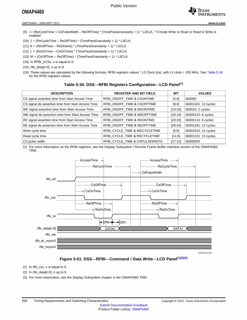
rfbi_a0
rfbi_csx
rfbi_re
rfbi_data[n:0]
rfbi_we
rfbi_te_vsync0
rfbi_hsync0
DATA0 DATA1
CsOnTime
CsOffTime
ReOnTime
ReOffTime
CsPulseWidth
ReCycleTime
AccessTime
CsOnTime
CsOffTime
ReOnTime
ReOffTime
AccessTime
ReCycleTime
DR0 DR1
SWPS040-048
Public Version
OMAP4460
SWPS046A –JANUARY 2012 www.ti.com
(9) I = (ReCycleTime + CsPulseWidth – ReOffTime) * (TimeParaGranularity + 1) * L3CLK. * if mode Write to Read or Read to Write isenabled
(10) J = (ReCycleTime – ReOffTime) * (TimeParaGranularity + 1) * L3CLK
(11) K = (ReOffTime – ReOntime) * (TimeParaGranularity + 1) * L3CLK
(12) L = (ReOnTime – CsOnTime) * (TimeParaGranularity + 1) * L3CLK
(13) M = (CsOffTime – ReOffTime) * (TimeParaGranularity + 1) * L3CLK
(14) In RFBI_nCSx, x is equal to 0.
(15) rfbi_data[n:0], n up to 8
(16) These values are calculated by the following formula: RFBI registers values * L3 Clock (ns), with L3 clock = 200 MHz. See Table 5-34for the RFBI registers values.
Table 5-34. DSS—RFBI Registers Configuration—LCD Panel(1)
DESCRIPTION REGISTER AND BIT FIELD BIT VALUES
CS signal assertion time from Start Access Time RFBI_ONOFF_TIME & CSONTIME [3:0] 0b0000
CS signal de-assertion time from Start Access Time RFBI_ONOFF_TIME & CSOFFTIME [9:4] 0b001101: 13 cycles
WE signal assertion time from Start Access Time RFBI_ONOFF_TIME & WEONTIME [13:10] 0b0010: 2 cycles
WE signal de-assertion time from Start Access Time RFBI_ONOFF_TIME & WEOFFTIME [19:14] 0b000110: 6 cycles
RE signal assertion time from Start Access Time RFBI_ONOFF_TIME & RDONTIME [23:20] 0b000110: 6 cycles
RE signal de-assertion time from Start Access Time RFBI_ONOFF_TIME & REOFFTIME [29:24] 0b001101: 13 cycles
Write cycle time RFBI_CYCLE_TIME & WECYCLETIME [5:0] 0b001010: 10 cycles
Read cycle time RFBI_CYCLE_TIME & RECYCLETIME [11:6] 0b001101: 13 cycles
CS pulse width RFBI_CYCLE_TIME & CSPULSEWIDTH [17:12] 0b000000
(1) For more information on the RFBI registers, see the Display Subsystem / Remote Frame Buffer Interface section of the OMAP4460TRM.
Figure 5-51. DSS—RFBI—Command / Data Write—LCD Panel(1)(2)(3)
(1) In rfbi_csx, x is equal to 0.
(2) In rfbi_data[n:0], n up to 8
(3) For more information, see the Display Subsystem chapter in the OMAP4460 TRM.
256 Timing Requirements and Switching Characteristics Copyright © 2012, Texas Instruments Incorporated
Submit Documentation FeedbackProduct Folder Link(s): OMAP4460

rfbi_a0
rfbi_csx
rfbi_we
rfbi_data[n:0]
rfbi_re
rfbi_te_vsync0
rfbi_hsync0
DATA0 DATA1
CsOnTime
CsOffTime
WeOnTime
WeOffTime
CsOnTime
CsOffTime
WeOnTime
WeOffTime
CsPulseWidth
WeCycleTime WeCycleTime
SWPS040-049
rfbi_a0
rfbi_csx
rfbi_we
rfbi_re
rfbi_data[n:0]
rfbi_te_vsync0
rfbi_hsync0
WRITE READ WRITE
CsOnTime
CsOffTime
WEOnTime
WEOffTime
WECylceTime
CsPulseWidth
ReCylceTime
AccessTime
CsOnTime
CsOffTime
ReOnTime
ReOffTime
CsPulseWidth
CsOnTime
WEOnTime
WEOffTime
CsOffTime
WECylceTime
SWPS040-050
Public Version
OMAP4460
www.ti.com SWPS046A –JANUARY 2012
Figure 5-52. DSS—RFBI—Command / Data Read—LCD Panel(1)(2)(3)
(1) In rfbi_csx, x is equal to 0.
(2) In rfbi_data[n:0], n up to 8
(3) For more information, see the Display Subsystem chapter in the OMAP4460 TRM.
Figure 5-53. DSS—RFBI—Command / DataWrite to Read and Read to Write—LCD Panel(1)(2)(3)
(1) In rfbi_csx, x is equal to 0.
(2) In rfbi_data[n:0], n up to 8
(3) For more information, see the Display Subsystem chapter in the OMAP4460 TRM.
Copyright © 2012, Texas Instruments Incorporated Timing Requirements and Switching Characteristics 257Submit Documentation Feedback
Product Folder Link(s): OMAP4460

Public Version
OMAP4460
SWPS046A –JANUARY 2012 www.ti.com
5.5.2.2.2 DSS—Remote Frame Buffer Interface (RFBI)—Pico DLP
The Remote Frame Buffer Interface (RFBI) module can provide also the necessary control signals anddata to interface to the Pico DLP driver of the Pico DLP panel.
Table 5-36 assume testing over the recommended operating conditions and electrical characteristicconditions below (see Figure 5-54).
Table 5-35. DSS—RFBI Timing Conditions—Pico DLP(1)(2)(3)
TIMING CONDITION PARAMETER VALUE UNIT
MIN MAX
PCB Conditions
Number of external peripherals 1
Far end load 5 pF
Trace length 10 cm
Characteristics impedance 30 50 Ω
(1) IO settings: DS0 = 0.For more information, see Control Module / Control Module Functional Description/ Functional Register Description / Signal IntegrityParameter Control Registers with Pad Group Assignment / I/O cells with Configurable Output Driver Impedance section of theOMAP4460 TRM.
(2) In this table the rise and fall times are calculated for 20% to 80% of VDDS. For more information on the corresponding OMAP4 VDDSpower supply name, see Table 2-1, POWER [9] column with the ball name.
(3) To have an idea of the output OMAP4 ball load supported for this application, you can consider the following:Output OMAP4 ball load = Far End load + 1.34 pF/cm typical x trace length (cm).
Table 5-36. DSS—RFBI Switching Characteristics—Pico DLP(16)(17)(18)
NO. PARAMETER OPP100, OPP119 OPP50 UNIT
MIN MAX MIN MAX
tw(rfbi_wrH) Pulse duration, rfbi_we high A(1) A(1) ns
tw(rfbi_wrL) Pulse duration, rfbi_we low B(2) B(2) ns
td(rfbi_a0-rfbi_wrL) Delay time, rfbi_a0 transition to rfbi_we low C(3) C(3) ns
td(rfbi_wrH-rfbi_a0) Delay time, rfbi_we high to rfbi_a0 transition D(4) D(4) ns
td(rfbi_csx-rfbi_wrL) Delay time, rfbi_csx(14) low to rfbi_we low E(5) E(5) ns
td(rfbi_wrH-rfbi_csxH) Delay time, rfbi_we high to rfbi_csx(14) high F(6) F(6) ns
td(dataV) Output rfbi_data[n:0](15) valid G(7) G(7) ns
tsk(Skew) Skew between output write enable falling 15.6 15.6 nsrfbi_we and output rfbi_data[n:0](15) high orlow
td(rfbi_a0H-rfbi_rdL) Delay time, rfbi_a0 high to rfbi_re low H(8) H(8) ns
td(rfbi_rdlH-rfbi_a0) Delay time, rfbi_re high to rfbi_a0 transition I(9) I(9) ns
tw(rfbi_rdH) Pulse duration, rfbi_re high J(10) J(10) ns
tw(rfbi_rdL) Pulse duration, rfbi_re low K(11) K(11) ns
td(rfbi_rdL-rfbi_csxL) Delay time, rfbi_re low to rfbi_csx(14) low L(12) L(12) ns
td(rfbi_rdH-rfbi_csxH) Delay time, rfbi_re high to rfbi_csx(14) high M(13) M(13) ns
tR(rfbi_wr) Rise time, rfbi_we 7 7 ns
tF(rfbi_wr) Fall time, rfbi_we 7 7 ns
tR(rfbi_a0) Rise time, rfbi_a0 7 7 ns
tF(rfbi_a0) Fall time, rfbi_a0 7 7 ns
tR(rfbi_csx) Rise time, rfbi_csx(14) 7 7 ns
tF(rfbi_csx) Fall time, rfbi_csx(14) 7 7 ns
tR(rfbi_da) Rise time, rfbi_data[n:0](15) 7 7 ns
tF(rfbi_da) Fall time, rfbi_data[n:0](15) 7 7 ns
tR(rfbi_rd) Rise time, rfbi_re 7 7 ns
258 Timing Requirements and Switching Characteristics Copyright © 2012, Texas Instruments Incorporated
Submit Documentation FeedbackProduct Folder Link(s): OMAP4460
Public Version
OMAP4460
www.ti.com SWPS046A –JANUARY 2012
Table 5-36. DSS—RFBI Switching Characteristics—Pico DLP(16)(17)(18) (continued)
NO. PARAMETER OPP100, OPP119 OPP50 UNIT
MIN MAX MIN MAX
tF(rfbi_rd) Fall time, rfbi_re 7 7 ns
CsOnTime CS signal assertion time from Start Access 0(19) nsTime – RFBI_ONOFF_TIME1 Register
CsOffTime CS signal de-assertion time from Start 40(19) nsAccess Time – RFBI_ONOFF_TIME1Register
WeOnTime WE signal assertion time from Start Access 0(19) nsTime – RFBI_ONOFF_TIME1 Register
WeOffTime WE signal de-assertion time from Start 20(19) nsAccess Time – RFBI_ONOFF_TIME1Register
ReOnTime RE signal assertion time from Start Access - nsTime – RFBI_ONOFF_TIME1 Register
ReOffTime RE signal de-assertion time from Start - nsAccess Time – RFBI_ONOFF_TIME1Register
WeCycleTime Write cycle time – 40(19) nsRFBI_CYCLE_TIME1_Register
ReCycleTime Read cycle time – - nsRFBI_CYCLE_TIME1_Register
CsPulseWidth CS pulse width – 0(19) nsRFBI_CYCLE_TIME1_Register
(1) A = (WeCycleTime – WeOffTime) * (TimeParaGranularity + 1) * L3CLK
(2) B = (WeOffTime – WeOntime) * (TimeParaGranularity + 1) * L3CLK
(3) C = (WEOnTime) * (TimeParaGranularity + 1) * L3CLK
(4) D = (WeCycleTime + CsPulseWidth – WeOffTime) * (TimeParaGranularity + 1) * L3CLK* if mode Write to Read or Read to Write is enabled.
(5) E = (WeOnTime – CsOnTime) * (TimeParaGranularity + 1) * L3CLK
(6) F = (CsOffTime – WeOffTime) * (TimeParaGranularity + 1) * L3CLK
(7) G = (WeCycleTime) * (TimeParaGranularity + 1) * L3CLK
(8) H = (ReOnTime) * (TimeParaGranularity + 1) * L3CLK
(9) I = (ReCycleTime + CsPulseWidth – ReOffTime) * (TimeParaGranularity + 1) * L3CLK* if mode Write to Read or Read to Write is enabled.
(10) J = (ReCycleTime – ReOffTime) * (TimeParaGranularity + 1) * L3CLK
(11) K = (ReOffTime – ReOntime) * (TimeParaGranularity + 1) * L3CLK
(12) L = (ReOnTime – CsOnTime) * (TimeParaGranularity + 1) * L3CLK
(13) M = (CsOffTime – ReOffTime) * (TimeParaGranularity + 1) * L3CLK
(14) In RFBI_nCSx, x is equal to 0.
(15) rfbi_data[n:0], n up to 15.
(16) See DM Operating Condition Addendum for CORE OPP voltages.
(17) At OPP100, L3 clock is 200 MHz and at OPP50, L3 clock is 100 MHz.
(18) rfbi_wr must be at 25 MHz.
(19) These values are calculated by the following formula: RFBI Register (Values) * L3 Clock (ns), with L3 clock = 200 MHz.See Table 5-37 for the RFBI registers values.
Copyright © 2012, Texas Instruments Incorporated Timing Requirements and Switching Characteristics 259Submit Documentation Feedback
Product Folder Link(s): OMAP4460
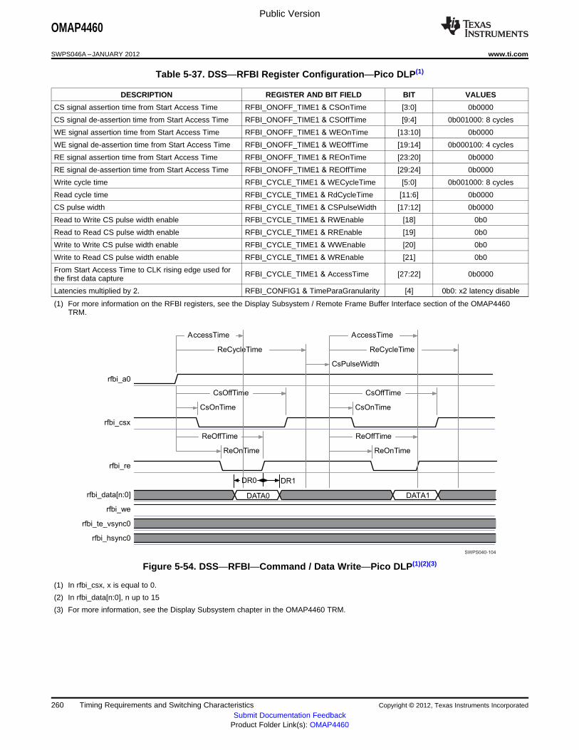
rfbi_a0
rfbi_csx
rfbi_re
rfbi_data[n:0]
rfbi_we
rfbi_te_vsync0
rfbi_hsync0
DATA0 DATA1
CsOnTime
CsOffTime
ReOnTime
ReOffTime
CsPulseWidth
ReCycleTime
AccessTime
CsOnTime
CsOffTime
ReOnTime
ReOffTime
AccessTime
ReCycleTime
DR0 DR1
SWPS040-104
Public Version
OMAP4460
SWPS046A –JANUARY 2012 www.ti.com
Table 5-37. DSS—RFBI Register Configuration—Pico DLP(1)
DESCRIPTION REGISTER AND BIT FIELD BIT VALUES
CS signal assertion time from Start Access Time RFBI_ONOFF_TIME1 & CSOnTime [3:0] 0b0000
CS signal de-assertion time from Start Access Time RFBI_ONOFF_TIME1 & CSOffTime [9:4] 0b001000: 8 cycles
WE signal assertion time from Start Access Time RFBI_ONOFF_TIME1 & WEOnTime [13:10] 0b0000
WE signal de-assertion time from Start Access Time RFBI_ONOFF_TIME1 & WEOffTime [19:14] 0b000100: 4 cycles
RE signal assertion time from Start Access Time RFBI_ONOFF_TIME1 & REOnTime [23:20] 0b0000
RE signal de-assertion time from Start Access Time RFBI_ONOFF_TIME1 & REOffTime [29:24] 0b0000
Write cycle time RFBI_CYCLE_TIME1 & WECycleTime [5:0] 0b001000: 8 cycles
Read cycle time RFBI_CYCLE_TIME1 & RdCycleTime [11:6] 0b0000
CS pulse width RFBI_CYCLE_TIME1 & CSPulseWidth [17:12] 0b0000
Read to Write CS pulse width enable RFBI_CYCLE_TIME1 & RWEnable [18] 0b0
Read to Read CS pulse width enable RFBI_CYCLE_TIME1 & RREnable [19] 0b0
Write to Write CS pulse width enable RFBI_CYCLE_TIME1 & WWEnable [20] 0b0
Write to Read CS pulse width enable RFBI_CYCLE_TIME1 & WREnable [21] 0b0
From Start Access Time to CLK rising edge used for RFBI_CYCLE_TIME1 & AccessTime [27:22] 0b0000the first data capture
Latencies multiplied by 2. RFBI_CONFIG1 & TimeParaGranularity [4] 0b0: x2 latency disable
(1) For more information on the RFBI registers, see the Display Subsystem / Remote Frame Buffer Interface section of the OMAP4460TRM.
Figure 5-54. DSS—RFBI—Command / Data Write—Pico DLP(1)(2)(3)
(1) In rfbi_csx, x is equal to 0.
(2) In rfbi_data[n:0], n up to 15
(3) For more information, see the Display Subsystem chapter in the OMAP4460 TRM.
260 Timing Requirements and Switching Characteristics Copyright © 2012, Texas Instruments Incorporated
Submit Documentation FeedbackProduct Folder Link(s): OMAP4460
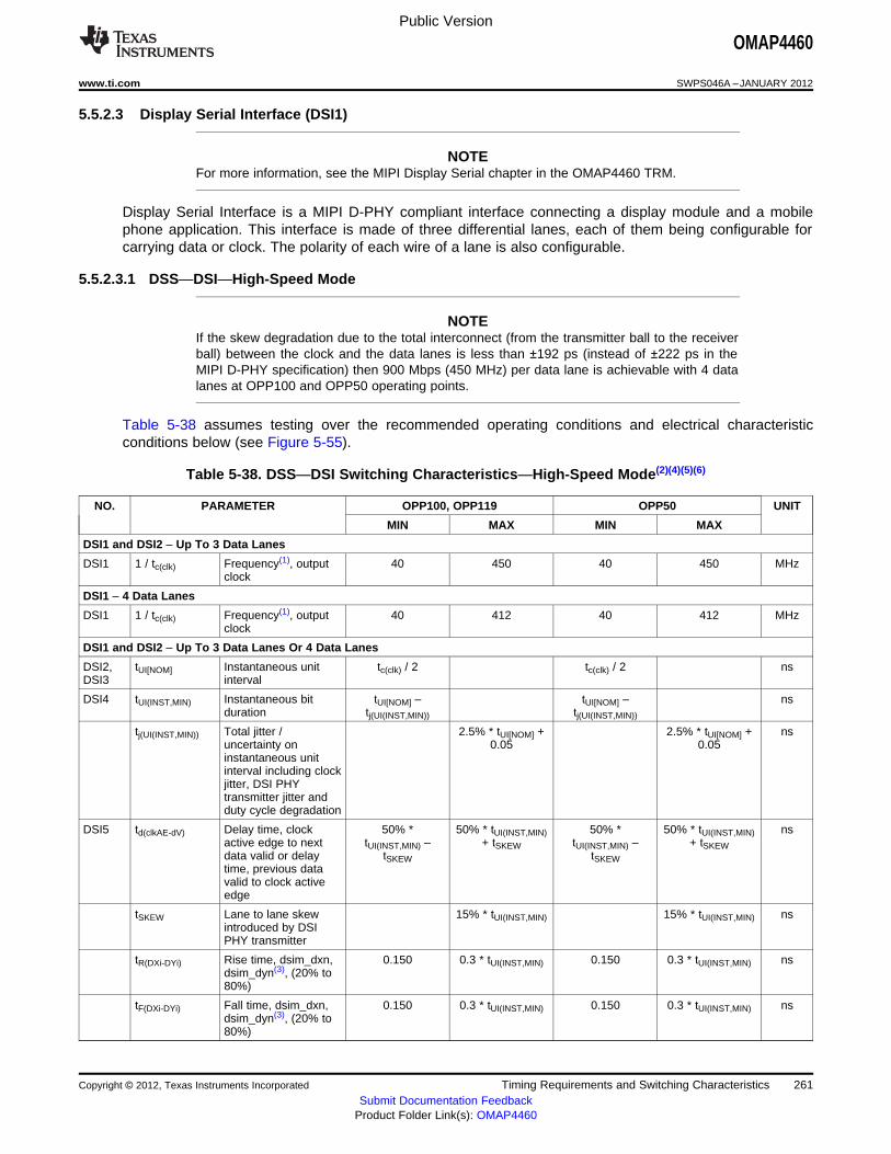
Public Version
OMAP4460
www.ti.com SWPS046A –JANUARY 2012
5.5.2.3 Display Serial Interface (DSI1)
NOTEFor more information, see the MIPI Display Serial chapter in the OMAP4460 TRM.
Display Serial Interface is a MIPI D-PHY compliant interface connecting a display module and a mobilephone application. This interface is made of three differential lanes, each of them being configurable forcarrying data or clock. The polarity of each wire of a lane is also configurable.
5.5.2.3.1 DSS—DSI—High-Speed Mode
NOTEIf the skew degradation due to the total interconnect (from the transmitter ball to the receiverball) between the clock and the data lanes is less than ±192 ps (instead of ±222 ps in theMIPI D-PHY specification) then 900 Mbps (450 MHz) per data lane is achievable with 4 datalanes at OPP100 and OPP50 operating points.
Table 5-38 assumes testing over the recommended operating conditions and electrical characteristicconditions below (see Figure 5-55).
Table 5-38. DSS—DSI Switching Characteristics—High-Speed Mode(2)(4)(5)(6)
NO. PARAMETER OPP100, OPP119 OPP50 UNIT
MIN MAX MIN MAX
DSI1 and DSI2 – Up To 3 Data Lanes
DSI1 1 / tc(clk) Frequency(1), output 40 450 40 450 MHzclock
DSI1 – 4 Data Lanes
DSI1 1 / tc(clk) Frequency(1), output 40 412 40 412 MHzclock
DSI1 and DSI2 – Up To 3 Data Lanes Or 4 Data Lanes
DSI2, tUI[NOM] Instantaneous unit tc(clk) / 2 tc(clk) / 2 nsDSI3 interval
DSI4 tUI(INST,MIN) Instantaneous bit tUI[NOM] – tUI[NOM] – nsduration tj(UI(INST,MIN)) tj(UI(INST,MIN))
tj(UI(INST,MIN)) Total jitter / 2.5% * tUI[NOM] + 2.5% * tUI[NOM] + nsuncertainty on 0.05 0.05instantaneous unitinterval including clockjitter, DSI PHYtransmitter jitter andduty cycle degradation
DSI5 td(clkAE-dV) Delay time, clock 50% * 50% * tUI(INST,MIN) 50% * 50% * tUI(INST,MIN) nsactive edge to next tUI(INST,MIN) – + tSKEW tUI(INST,MIN) – + tSKEWdata valid or delay tSKEW tSKEWtime, previous datavalid to clock activeedge
tSKEW Lane to lane skew 15% * tUI(INST,MIN) 15% * tUI(INST,MIN) nsintroduced by DSIPHY transmitter
tR(DXi-DYi) Rise time, dsim_dxn, 0.150 0.3 * tUI(INST,MIN) 0.150 0.3 * tUI(INST,MIN) nsdsim_dyn(3), (20% to80%)
tF(DXi-DYi) Fall time, dsim_dxn, 0.150 0.3 * tUI(INST,MIN) 0.150 0.3 * tUI(INST,MIN) nsdsim_dyn(3), (20% to80%)
Copyright © 2012, Texas Instruments Incorporated Timing Requirements and Switching Characteristics 261Submit Documentation Feedback
Product Folder Link(s): OMAP4460

dsi_dwn
dsi_dwn
dsi_dwn
Data (j-1) Data_j Data_(j+1)
Data (k-1) Data_k Data_(k+1)
DSI4
DSI5
DSI1
DSI2DSI3
DSI4
DSI5 DSI5 DSI5
SWPS040-051
Public Version
OMAP4460
SWPS046A –JANUARY 2012 www.ti.com
(1) Related to the maximum frequency supported by the DSI module.
(2) The timing requirements are assured up to the minimum instantaneous bit duration.
(3) In dsim_dxn and dsim_dyn, m is equal to 1 or 2, and n is equal to 0, 1, 2, 3, or 4 for DSI1 and n is equal to 0, 1, or 2 for DSI2.
(4) No specific capacitive load is needed in DSI high-speed mode. The PCB interconnect must be 50-Ω transmission line on DSIdsim_dx[2;0] and DSI dsim_dy[2;0]. DSI dsim_dx[2;0] and DSI dsi_dy[2;0] lines must be well matched. See Chapter 7 of the MIPID-PHY standard v1.0 for completes specification of the Interconnect.
(5) See DM Operating Condition Addendum for CORE OPP voltages.
(6) For more information on the PCB requirements, see Section A.4.3, MIPI D-PHY PCB Guidelines in OMAP4.
Figure 5-55. DSS—DSI—High-Speed Mode(1)(2)(3)
(1) In dsim_dwn, w is equal to x or y, m is equal to 1 or 2, and n is equal to 0, 1, 2, 3, or 4 for DSI1 and n is equal to 0, 1, or 2 for DSI2.
(2) The use of each dsim_dwn(1) lane (clock or data) is software programmable with the DSI_COMPLEXIO_CFG1 register. For moreinformation, see the Display Subsystem chapter in the OMAP4460 TRM.
(3) The polarity of each dsim_dwn(1) lane is software programmable with the DSI_COMPLEXIO_CFG1 register. For more information, seethe Display Subsystem chapter in the OMAP4460 TRM.
5.5.2.3.2 DSS—DSI—Low-Power and Ultralow-Power Modes
Table 5-40 assumes testing over the recommended operating conditions and electrical characteristicconditions below (see Figure 5-56).
Table 5-39. DSS—DSI Timing Conditions—Low-Power and Ultralow-Power Modes(3)
TIMING CONDITION PARAMETER VALUE UNIT
MIN MAX
Output Condition
CLOAD Output load capacitance 0 60(1) pF
(1) The maximum capacitive load for the DSI low-power mode is equal to 60 pF. See Chapter 8 of the MIPI D-PHY standard v1.0 forcomplete specification on the electrical characteristics. The PCB interconnect must be 50-Ω transmission line on DSI dsim_dx[n;0](2) andDSI dsim_dy[n;0](2). DSI dsim_dx[n;0](2) and DSI dsim_dy[n;0](2) lines must be well matched. See Chapter 7 of the MIPI D-PHY standardv1.0 for complete specification of the interconnect.
(2) In dsim_dxn and dsim_dyn, m is equal to 1 or 2, and n is equal to 0, 1, 2, 3, or 4 for DSI1 and n is equal to 0, 1, or 2 for DSI2.
(3) For more information on the PCB requirements, see Section A.4.3, MIPI D-PHY PCB Guidelines in OMAP4
Table 5-40. DSI Switching Characteristics—Low-Power and Ultralow-Power Modes(5)
NO. PARAMETER OPP100, OPP119 OPP50 UNIT
MIN MAX MIN MAX
DSI6 tw(XORclk) Pulse width of the LP First LP exclusive-OR 40 40 nsexclusive-OR clock(1) clock(1) pulse after Stop
state or last pulsebefore Stop state
All other pulses 20 20 ns
tc(XORclk) Period of the LP exclusive-OR clock(1) 90 90 ns
tREOT(LP) Rise time, dsim_dxn, dsim_dyn(4) 35 35 ns
262 Timing Requirements and Switching Characteristics Copyright © 2012, Texas Instruments Incorporated
Submit Documentation FeedbackProduct Folder Link(s): OMAP4460

dsim_dxn
dsmi_dyn
mark_j-1space_j-1
mark_jspace_j
mark_j+1
mark_k-1sapce_k-1
mark_kspace_k
mark_k+1
DSI6
DSI6
DSI6
SWPS040-052
Public Version
OMAP4460
www.ti.com SWPS046A –JANUARY 2012
Table 5-40. DSI Switching Characteristics—Low-Power and Ultralow-Power Modes(5) (continued)
NO. PARAMETER OPP100, OPP119 OPP50 UNIT
MIN MAX MIN MAX
tR(LP) Rise time, dsim_dxn, dsim_dyn(2)(3) for a 5-pF CL 2.6 25 2.6 25 nsload
Rise time, dsim_dxn, dsim_dyn(2)(3) for a 20-pF 3.1 25 3.1 25CL load
Rise time, dsim_dxn, dsim_dyn(2)(3) for a 70-pF 5.1 25 5.1 25CL load
tF(LP) Fall time, dsim_dxn, dsim_dyn(2)(3) or a 5-pF CL 2.6 25 2.6 25 nsload
Fall time, dsim_dxn, dsim_dyn(2)(3) or a 20-pF CL 3.1 25 3.1 25load
Fall time, dsim_dxn, dsim_dyn(2)(3) or a 70-pF CL 5.1 25 5.1 25load
(1) Low-power and ultralow-power communication modes are asynchronous, data is Spaced-One-Hot bit encoded, data transfer clock isrecovered by means of an XOR between dsim_dxn(2) and dsim_dyn(2). For more information about the LP exclusive-OR clock, seeTable 19 of MIPI D-PHY standard v1.0.
(2) In dsim_dxn and dsim_dyn, m is equal to 1 or 2, and n is equal to 0, 1, 2, 3, or 4 for DSI1 and n is equal to 0, 1, or 2 for DSI2.
(3) The output rise and fall times are measured between 15% and 85% of vdds_dsi.
(4) Rise or fall time between 30% and 85% of the low-power (LP) levels. This is applicable only when high-speed (HS) burst is ending, thatis, the lines go from a high-speed state 0 or a high-speed state 1 to a low-power stop state (the differential drive is stopped). Since thereis extra load on the lines (the receiver in low-power mode has a common mode capacitor of up to 60 pF), this is slower. See theLow-Power Receiver Mode (LPRX) section of Table 3-8 for the Low-Power VIL/VOL input threshold values.
(5) See DM Operating Condition Addendum for CORE OPP voltages.
Figure 5-56. DSS—DSI—Low-Power and Ultralow-Power Modes(1)(2)
(1) In dsim_dwn, w is equal to x or y, m is equal to 1 or 2, and n is equal to 0, 1, 2, 3, or 4 for DSI1 and n is equal to 0, 1, or 2 for DSI2.
(2) Low-Power and Ultralow-Power communication modes are asynchronous, data is Spaced-One-Hot bit encoded, data transfer clock isrecovered by means of an XOR between dsim_dxn(1) and dsim_dyn(1).
5.5.2.4 High Definition Multimedia Interface (HDMI)
NOTEFor more information on HDMI, please contact your TI representative.
5.6 Serial Communications Interfaces
5.6.1 Multichannel Buffered Serial Port (McBSP)
NOTEFor more information, see the Serial Communication Interface / Multichannel Buffered SerialPort (McBSP) / McBSP Functional Description section of the OMAP4460 TRM.
The multichannel buffered serial port (McBSP) provides a full-duplex direct serial interface between theOMAP chip and other devices in a system, such as other application chips, codecs. It can accommodate awide range of peripherals and clocked frame oriented protocols ( I2S™, PCM, TDM) due to its high levelof versatility.
Copyright © 2012, Texas Instruments Incorporated Timing Requirements and Switching Characteristics 263Submit Documentation Feedback
Product Folder Link(s): OMAP4460

Public Version
OMAP4460
SWPS046A –JANUARY 2012 www.ti.com
McBSP supports two types of data transfer at the system level:• The full-cycle mode, for which one clock period is used to transfer the data, generated on one edge
and captured on the same edge (one clock period later).• The half-cycle mode, for which one-half clock period is used to transfer the data, generated on one
edge and captured on the opposite edge (one-half clock period later). Note that a new data isgenerated only every clock period, which secures the required hold time.
The interface clock (clkX/CLKR) activation edge (data/frame sync capture and generation) has to beconfigured accordingly with the external peripheral (activation edge capability) and the type of datatransfer required at the system level.
Depending on the number of pins, McBSP supports either:• 6-pin mode: dx and dr as data pins; clkx, clkr, fsx, and fsr as control pins.• 4-pin mode: dx and dr as data pins; clkx and fsx pins as control pins. The clkx and fsx pins are
internally looped back, via software configuration, respectively to the clkr and fsr internal signals fordata receive.
5.6.1.1 McBSP1, McBSP2, and McBSP3 Set#1
5.6.1.1.1 McBSP1, McBSP2, and McBSP3 Set#1—I2S/PCM
Table 5-42 through Table 5-45 assume testing over the recommended operating conditions and electricalcharacteristic conditions below (see Figure 5-57 and Figure 5-58).
Table 5-41. McBSP1, 2 Timing Conditions—I2S/PCM(1)(2)(3)
SYSTEM CONDITION PARAMETER VALUE UNIT
MIN MAX
Input Conditions
tR Input signal rise time 400 6500 ps
tF Input signal fall time 400 6500 ps
PCB Conditions
Number of external peripherals 1
Far end load 5 pF
Trace length 9 cm
Characteristics impedance 30 55 Ω
(1) IO settings: MB[1:0] = 10 and LB0 = 0.For more information, see Control Module / Control Module Functional Description/ Functional Register Description / Signal IntegrityParameter Control Registers with Pad Group Assignment / 50-Ω Output Buffer I/Os with Combined Mode and Load Settings section ofthe OMAP4460 TRM.
(2) In this table the rise and fall times are calculated for 10% to 90% of VDDS. For more information on the corresponding OMAP4 VDDSpower supply name, see Table 2-1, POWER [9] column with the ball name.
(3) To have an idea of the output OMAP4 ball load supported for this application, you can consider the following:Output OMAP4 ball load = Far End load + 1.34 pF/cm typical x trace length (cm).
5.6.1.1.1.1 McBSP1 and McBSP2—I2S/PCM Full and Half Cycle—Master Mode—24 MHz
Table 5-42. McBSP1, 2 Timing Requirements—I2S/PCM—Master Mode(1)(3)(6)
NO. PARAMETER OPP100, OPP119 OPP50 UNIT
MIN MAX MIN MAX
1 / tc(clks) Frequency, input abe_clks(5) clock 24.576(5) 12.288(5) MHz
tw(clksL) Typical pulse duration, input abe_clks low 0.5 * P(4) 0.5 * P(4) ns
tw(clksH) Typical pulse duration, output abe_clks high 0.5 * P(4) 0.5 * P(4) ns
tdc(clks) Duty cycle error, input abe_clks –0.05 * 0.05 * –0.05 * 0.05 * psP(4) + 610 P(4) – 610 P(4) + 610 P(4) – 610
264 Timing Requirements and Switching Characteristics Copyright © 2012, Texas Instruments Incorporated
Submit Documentation FeedbackProduct Folder Link(s): OMAP4460
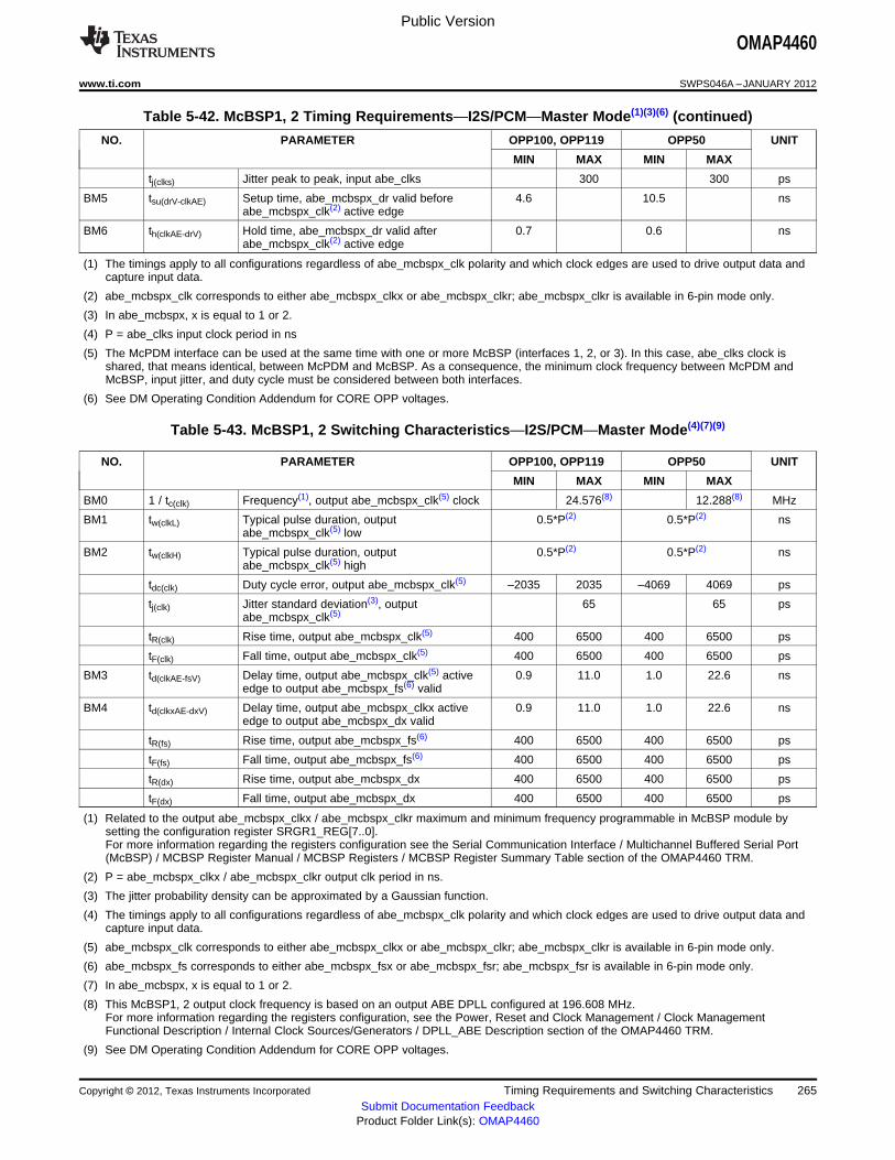
Public Version
OMAP4460
www.ti.com SWPS046A –JANUARY 2012
Table 5-42. McBSP1, 2 Timing Requirements—I2S/PCM—Master Mode(1)(3)(6) (continued)
NO. PARAMETER OPP100, OPP119 OPP50 UNIT
MIN MAX MIN MAX
tj(clks) Jitter peak to peak, input abe_clks 300 300 ps
BM5 tsu(drV-clkAE) Setup time, abe_mcbspx_dr valid before 4.6 10.5 nsabe_mcbspx_clk(2) active edge
BM6 th(clkAE-drV) Hold time, abe_mcbspx_dr valid after 0.7 0.6 nsabe_mcbspx_clk(2) active edge
(1) The timings apply to all configurations regardless of abe_mcbspx_clk polarity and which clock edges are used to drive output data andcapture input data.
(2) abe_mcbspx_clk corresponds to either abe_mcbspx_clkx or abe_mcbspx_clkr; abe_mcbspx_clkr is available in 6-pin mode only.
(3) In abe_mcbspx, x is equal to 1 or 2.
(4) P = abe_clks input clock period in ns
(5) The McPDM interface can be used at the same time with one or more McBSP (interfaces 1, 2, or 3). In this case, abe_clks clock isshared, that means identical, between McPDM and McBSP. As a consequence, the minimum clock frequency between McPDM andMcBSP, input jitter, and duty cycle must be considered between both interfaces.
(6) See DM Operating Condition Addendum for CORE OPP voltages.
Table 5-43. McBSP1, 2 Switching Characteristics—I2S/PCM—Master Mode(4)(7)(9)
NO. PARAMETER OPP100, OPP119 OPP50 UNIT
MIN MAX MIN MAX
BM0 1 / tc(clk) Frequency(1), output abe_mcbspx_clk(5) clock 24.576(8) 12.288(8) MHz
BM1 tw(clkL) Typical pulse duration, output 0.5*P(2) 0.5*P(2) nsabe_mcbspx_clk(5) low
BM2 tw(clkH) Typical pulse duration, output 0.5*P(2) 0.5*P(2) nsabe_mcbspx_clk(5) high
tdc(clk) Duty cycle error, output abe_mcbspx_clk(5) –2035 2035 –4069 4069 ps
tj(clk) Jitter standard deviation(3), output 65 65 psabe_mcbspx_clk(5)
tR(clk) Rise time, output abe_mcbspx_clk(5) 400 6500 400 6500 ps
tF(clk) Fall time, output abe_mcbspx_clk(5) 400 6500 400 6500 ps
BM3 td(clkAE-fsV) Delay time, output abe_mcbspx_clk(5) active 0.9 11.0 1.0 22.6 nsedge to output abe_mcbspx_fs(6) valid
BM4 td(clkxAE-dxV) Delay time, output abe_mcbspx_clkx active 0.9 11.0 1.0 22.6 nsedge to output abe_mcbspx_dx valid
tR(fs) Rise time, output abe_mcbspx_fs(6) 400 6500 400 6500 ps
tF(fs) Fall time, output abe_mcbspx_fs(6) 400 6500 400 6500 ps
tR(dx) Rise time, output abe_mcbspx_dx 400 6500 400 6500 ps
tF(dx) Fall time, output abe_mcbspx_dx 400 6500 400 6500 ps
(1) Related to the output abe_mcbspx_clkx / abe_mcbspx_clkr maximum and minimum frequency programmable in McBSP module bysetting the configuration register SRGR1_REG[7..0].For more information regarding the registers configuration see the Serial Communication Interface / Multichannel Buffered Serial Port(McBSP) / MCBSP Register Manual / MCBSP Registers / MCBSP Register Summary Table section of the OMAP4460 TRM.
(2) P = abe_mcbspx_clkx / abe_mcbspx_clkr output clk period in ns.
(3) The jitter probability density can be approximated by a Gaussian function.
(4) The timings apply to all configurations regardless of abe_mcbspx_clk polarity and which clock edges are used to drive output data andcapture input data.
(5) abe_mcbspx_clk corresponds to either abe_mcbspx_clkx or abe_mcbspx_clkr; abe_mcbspx_clkr is available in 6-pin mode only.
(6) abe_mcbspx_fs corresponds to either abe_mcbspx_fsx or abe_mcbspx_fsr; abe_mcbspx_fsr is available in 6-pin mode only.
(7) In abe_mcbspx, x is equal to 1 or 2.
(8) This McBSP1, 2 output clock frequency is based on an output ABE DPLL configured at 196.608 MHz.For more information regarding the registers configuration, see the Power, Reset and Clock Management / Clock ManagementFunctional Description / Internal Clock Sources/Generators / DPLL_ABE Description section of the OMAP4460 TRM.
(9) See DM Operating Condition Addendum for CORE OPP voltages.
Copyright © 2012, Texas Instruments Incorporated Timing Requirements and Switching Characteristics 265Submit Documentation Feedback
Product Folder Link(s): OMAP4460

Public Version
OMAP4460
SWPS046A –JANUARY 2012 www.ti.com
5.6.1.1.1.2 McBSP1 and McBSP2—I2S/PCM Full and Half Cycle—Slave Mode—12 MHz
Table 5-44. McBSP1, 2 Timing Requirements—I2S/PCM—Slave Mode(4)(5)(8)(9)
NO. PARAMETER OPP100, OPP119 OPP50 UNIT
MIN MAX MIN MAX
BS0 1 / tc(clk) Frequency(1), abe_mcbspx_clk(6) 12.288 6.144 MHz
BS1 tw(clkL) Typical pulse duration, abe_mcbspx_clk(6) low 0.5*P(2) 0.5*P(2) ns
BS2 tw(clkH) Typical pulse duration, abe_mcbspx_clk(6) high 0.5*P(2) 0.5*P(2) ns
tdc(clk) Duty cycle error, abe_mcbspx_clk(6) –2035 2035 –4069 4069 ps
tj(clk) Cycle jitter(3), abe_mcbspx_clk(6) 1221 2000 ps
BS3 tsu(fsV-clkAE) Setup time, abe_mcbspx_fs(7) valid before 14.3 30.4 nsabe_mcbspx_clk(6) active edge
BS4 th(clkAE-fsV) Hold time, abe_mcbspx_fs(7) valid after 14.3 30.4 nsabe_mcbspx_clk(6) active edge
BS6 tsu(drV-clkAE) Setup time, abe_mcbspx_dr valid before 14.3 30.4 nsabe_mcbspx_clk(6) active edge
BS7 th(clkAE-drV) Hold time, abe_mcbspx_dr valid after 14.3 30.4 nsabe_mcbspx_clk(6) active edge
(1) Related to the input maximum frequency supported by the McBSP module.
(2) P = abe_mcbspx_clkx / abe_mcbspx_clkr period in ns
(3) Maximum cycle jitter supported by abe_mcbspx_clkx / abe_mcbspx_clkr input clock.
(4) The timing requirements are assured for the cycle jitter and duty cycle error conditions specified.
(5) The timings apply to all configurations regardless of abe_mcbspx_clk polarity and which clock edges are used to drive output data andcapture input data.
(6) abe_mcbspx_clk corresponds to either abe_mcbspx_clkx or abe_mcbspx_clkr; abe_mcbspx_clkr is available in 6-pin mode only.
(7) abe_mcbspx_fs corresponds to either abe_mcbspx_fsx or abe_mcbspx_fsr; abe_mcbspx_fsr is available in 6-pin mode only.
(8) In abe_mcbspx, x is equal to 1 or 2.
(9) See DM Operating Condition Addendum for CORE OPP voltages.
Table 5-45. McBSP1, 2 Switching Characteristics—I2S/PCM—Slave Mode(1)(2)(3)
NO. PARAMETER OPP100, OPP119 OPP50 UNIT
MIN MAX MIN MAX
BS5 td(clkxAE-dxV) Delay time, input abe_mcbspx_clkx active –16.4 20.3 –34.0 36.1 nsedge to output abe_mcbspx_dx valid
tR(dx) Rise time, output abe_mcbspx_dx 400 6500 400 6500 ps
tF(dx) Fall time, output abe_mcbspx_dx 400 6500 400 6500 ps
266 Timing Requirements and Switching Characteristics Copyright © 2012, Texas Instruments Incorporated
Submit Documentation FeedbackProduct Folder Link(s): OMAP4460
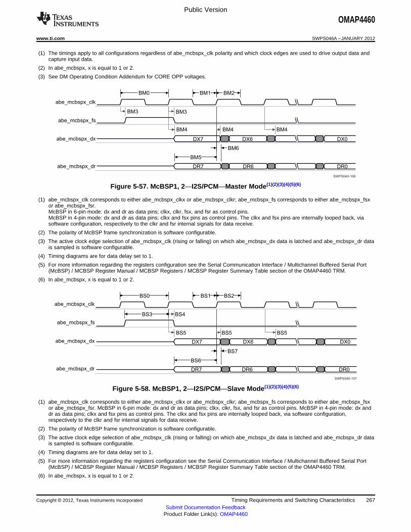
abe_mcbspx_clk
abe_mcbspx_fs
abe_mcbspx_dx
abe_mcbspx_dr
DX7 DX6 DX0
DR7 DR6 DR0
BM3 BM3
BM4
BM0 BM1 BM2
BM5
BM6
SWPS040-106
BM4 BM4
abe_mcbspx_clk
abe_mcbspx_fs
abe_mcbspx_dx
abe_mcbspx_dr
DX7 DX6 DX0
DR7 DR6 DR0
BS4
BS5
BS0 BS1 BS2
BS6
BS7
BS5 BS5
BS3
SWPS040-107
Public Version
OMAP4460
www.ti.com SWPS046A –JANUARY 2012
(1) The timings apply to all configurations regardless of abe_mcbspx_clk polarity and which clock edges are used to drive output data andcapture input data.
(2) In abe_mcbspx, x is equal to 1 or 2.
(3) See DM Operating Condition Addendum for CORE OPP voltages.
Figure 5-57. McBSP1, 2—I2S/PCM—Master Mode(1)(2)(3)(4)(5)(6)
(1) abe_mcbspx_clk corresponds to either abe_mcbspx_clkx or abe_mcbspx_clkr; abe_mcbspx_fs corresponds to either abe_mcbspx_fsxor abe_mcbspx_fsr.McBSP in 6-pin mode: dx and dr as data pins; clkx, clkr, fsx, and fsr as control pins.McBSP in 4-pin mode: dx and dr as data pins; clkx and fsx pins as control pins. The clkx and fsx pins are internally looped back, viasoftware configuration, respectively to the clkr and fsr internal signals for data receive.
(2) The polarity of McBSP frame synchronization is software configurable.
(3) The active clock edge selection of abe_mcbspx_clk (rising or falling) on which abe_mcbspx_dx data is latched and abe_mcbspx_dr datais sampled is software configurable.
(4) Timing diagrams are for data delay set to 1.
(5) For more information regarding the registers configuration see the Serial Communication Interface / Multichannel Buffered Serial Port(McBSP) / MCBSP Register Manual / MCBSP Registers / MCBSP Register Summary Table section of the OMAP4460 TRM.
(6) In abe_mcbspx, x is equal to 1 or 2.
Figure 5-58. McBSP1, 2—I2S/PCM—Slave Mode(1)(2)(3)(4)(5)(6)
(1) abe_mcbspx_clk corresponds to either abe_mcbspx_clkx or abe_mcbspx_clkr; abe_mcbspx_fs corresponds to either abe_mcbspx_fsxor abe_mcbspx_fsr. McBSP in 6-pin mode: dx and dr as data pins; clkx, clkr, fsx, and fsr as control pins. McBSP in 4-pin mode: dx anddr as data pins; clkx and fsx pins as control pins. The clkx and fsx pins are internally looped back, via software configuration,respectively to the clkr and fsr internal signals for data receive.
(2) The polarity of McBSP frame synchronization is software configurable.
(3) The active clock edge selection of abe_mcbspx_clk (rising or falling) on which abe_mcbspx_dx data is latched and abe_mcbspx_dr datais sampled is software configurable.
(4) Timing diagrams are for data delay set to 1.
(5) For more information regarding the registers configuration see the Serial Communication Interface / Multichannel Buffered Serial Port(McBSP) / MCBSP Register Manual / MCBSP Registers / MCBSP Register Summary Table section of the OMAP4460 TRM.
(6) In abe_mcbspx, x is equal to 1 or 2.
Copyright © 2012, Texas Instruments Incorporated Timing Requirements and Switching Characteristics 267Submit Documentation Feedback
Product Folder Link(s): OMAP4460

Public Version
OMAP4460
SWPS046A –JANUARY 2012 www.ti.com
5.6.1.1.2 McBSP1, McBSP2, and McBSP3 Set#1—TDM / Half-Cycle
5.6.1.1.2.1 McBSP1, McBSP2, and McBSP3 Set#1—TDM / Half-Cycle—6MHz, 40-pF Load Capacitance
Table 5-47 through Table 5-50 assume testing over the recommended operating conditions and electricalcharacteristic conditions below (see Figure 5-59 and Figure 5-60).
Table 5-46. McBSP1, McBSP2, and McBSP3 Set#1 Timing Conditions—TDM / Half-Cycle(1)(2)(3)
SYSTEM CONDITION PARAMETER VALUE UNIT
MIN MAX
Input Conditions
tR Input signal rise time 1000 11100 ps
tF Input signal fall time 1000 11100 ps
PCB Conditions
Number of external peripherals 1
Far end load 40 pF
Trace length 9 cm
Characteristics impedance 20 60 Ω
(1) IO settings: MB[1:0] = 10 and LB0 = 0 McBSP3 Set#1 means the following balls: AG25, AF25, AE25, AF26.For more information, see Control Module / Control Module Functional Description/ Functional Register Description / Signal IntegrityParameter Control Registers with Pad Group Assignment / 50-Ω Output Buffer I/Os with Combined Mode and Load Settings section ofthe OMAP4460 TRM.
(2) In this table the rise and fall times are calculated for 10% to 90% of VDDS. For more information on the corresponding OMAP4 VDDSpower supply name, see Table 2-1, POWER [9] column with the ball name.
(3) To have an idea of the output OMAP4 ball load supported for this application, you can consider the following:Output OMAP4 ball load = Far End load + 1.34 pF/cm typical x trace length (cm).
5.6.1.1.2.1.1 McBSP1, McBSP2, and McBSP3 Set#1—TDM / Half-Cycle—Master Mode
Table 5-47. McBSP1, McBSP2, and McBSP3 Set#1 Timing Requirements—TDM / Half-Cycle—MasterMode(1)(3)(6)
NO. PARAMETER OPP100, OPP119 OPP50 UNIT
MIN MAX MIN MAX
1 / tc(clks) Frequency, input abe_clks(5) clock 6.144(5) 3.072(5) MHz
tw(clksL) Typical pulse duration, input abe_clks low 0.5 * P(4) 0.5 * P(4) ns
tw(clksH) Typical pulse duration, output abe_clks high 0.5 * P(4) 0.5 * P(4) ns
tdc(clks) Duty cycle error, input abe_clks –0.05 * 0.05 * –0.05 * 0.05 * psP(4) + 610 P(4) – 610 P(4) + 610 P(4) – 610
tj(clks) Jitter peak to peak, input abe_clks 300 300 ps
BM5 tsu(drV-clkAE) Setup time, abe_mcbspx_dr valid before 22.6 48.6 nsabe_mcbspx_clk(2) active edge
BM6 th(clkAE-drV) Hold time, abe_mcbspx_dr valid after 22.3 48.4 nsabe_mcbspx_clk(2) active edge
(1) The timings apply to all configurations regardless of abe_mcbspx_clk polarity and which clock edges are used to drive output data andcapture input data.
(2) abe_mcbspx_clk corresponds to either abe_mcbspx_clkx or abe_mcbspx_clkr; abe_mcbspx_clkr is available in 6-pin mode only.
(3) In abe_mcbspx, x is equal to 1 or, 2 or, 3 Set#1 (Balls: AG25, AF25, AE25, AF26).
(4) P = abe_clks input clock period in ns
(5) The McPDM interface can be used at the same time with one or more McBSP (interface 1, 2, or 3). In this case, abe_clks clock isshared, that means identical, between McPDM and McBSP. As a consequence, the minimum clock frequency between McPDM andMcBSP, input jitter, and duty cycle must be considered between both interfaces.
(6) See DM Operating Condition Addendum for CORE OPP voltages.
Table 5-48. McBSP1, McBSP2, and McBSP3 Set#1 Switching Characteristics—TDM / Half-Cycle—Master
268 Timing Requirements and Switching Characteristics Copyright © 2012, Texas Instruments Incorporated
Submit Documentation FeedbackProduct Folder Link(s): OMAP4460

Public Version
OMAP4460
www.ti.com SWPS046A –JANUARY 2012
Table 5-48. McBSP1, McBSP2, and McBSP3 Set#1 Switching Characteristics—TDM / Half-Cycle—MasterMode(4)(7)(9) (continued)
Mode(4)(7)(9)
NO. PARAMETER OPP100, OPP119 OPP50 UNIT
MIN MAX MIN MAX
BM0 1 / tc(clk) Frequency(1), output abe_mcbspx_clk(5) clock 6.144(8) 3.072(8) MHz
BM1 tw(clkL) Typical pulse duration, output 0.5*P(2) 0.5*P(2) nsabe_mcbspx_clk(5) low
BM2 tw(clkH) Typical pulse duration, output 0.5*P(2) 0.5*P(2) nsabe_mcbspx_clk(5) high
tdc(clk) Duty cycle error, output abe_mcbspx_clk(5) –8138 8138 –16276 16276 ps
tj(clk) Jitter standard deviation(3), output 65 65 psabe_mcbspx_clk(5)
tR(clk) Rise time, output abe_mcbspx_clk(5) 1000 11100 1000 11100 ps
tF(clk) Fall time, output abe_mcbspx_clk(5) 1000 11100 1000 11100 ps
BM3 td(clkAE-fsV) Delay time, output abe_mcbspx_clk(5) active –30.9 46.4 –63.5 94.4 nsedge to output abe_mcbspx_fs(6) valid
BM4 td(clkxAE-dxV) Delay time, output abe_mcbspx_clkx active –30.9 46.4 –63.5 94.4 nsedge to output abe_mcbspx_dx valid
tR(fs) Rise time, output abe_mcbspx_fs(6) 1000 11100 1000 11100 ps
tF(fs) Fall time, output abe_mcbspx_fs(6) 1000 11100 1000 11100 ps
tR(dx) Rise time, output abe_mcbspx_dx 1000 11100 1000 11100 ps
tF(dx) Fall time, output abe_mcbspx_dx 1000 11100 1000 11100 ps
(1) Related to the output abe_mcbspx_clkx / abe_mcbspx_clkr maximum and minimum frequency programmable in McBSP module bysetting the configuration register SRGR1_REG[7..0].For more information regarding the registers configuration see the Serial Communication Interface / Multichannel Buffered Serial Port(McBSP) / MCBSP Register Manual / MCBSP Registers / MCBSP Register Summary Table section of the OMAP4460 TRM.
(2) P = abe_mcbspx_clkx / abe_mcbspx_clkr output clk period in ns
(3) The jitter probability density can be approximated by a Gaussian function.
(4) The timings apply to all configurations regardless of abe_mcbspx_clk polarity and which clock edges are used to drive output data andcapture input data.
(5) abe_mcbspx_clk corresponds to either abe_mcbspx_clkx or abe_mcbspx_clkr; abe_mcbspx_clkr is available in 6-pin mode only.
(6) abe_mcbspx_fs corresponds to either abe_mcbspx_fsx or abe_mcbspx_fsr; abe_mcbspx_fsr is available in 6-pin mode only.
(7) In abe_mcbspx, x is equal to 1, 2, or 3 Set#1 (Balls: AG25, AF25, AE25, AF26).
(8) This McBSP1, 2 output clock frequency is based on an output ABE DPLL configured at 196.608 MHz.For more information regarding the registers configuration, see the Power, Reset and Clock Management / Clock ManagementFunctional Description / Internal Clock Sources/Generators / DPLL_ABE Description section of the OMAP4460 TRM.
(9) See DM Operating Condition Addendum for CORE OPP voltages.
5.6.1.1.2.1.2 McBSP1, McBSP2, and McBSP3 Set#1—TDM / Half-Cycle—Slave Mode
Table 5-49. McBSP1, 2, and 3 Set#1 Timing Requirements—TDM / Half-Cycle—Slave Mode(4)(5)(8)(9)
NO. PARAMETER OPP100, OPP119 OPP50 UNIT
MIN MAX MIN MAX
BS0 1 / tc(clk) Frequency(1), abe_mcbspx_clk(6) 6.144 3.072 MHz
BS1 tw(clkL) Typical pulse duration, abe_mcbspx_clk(6) low 0.5*P(2) 0.5*P(2) ns
BS2 tw(clkH) Typical pulse duration, abe_mcbspx_clk(6) 0.5*P(2) 0.5*P(2) nshigh
tdc(clk) Duty cycle error, abe_mcbspx_clk(6) –8138 8138 –16276 16276 ps
tj(clk) Cycle jitter(3), abe_mcbspx_clk(6) 2000 2000 ps
BS3 tsu(fsV-clkAE) Setup time, abe_mcbspx_fs(7) valid before 26.5 55.8 nsabe_mcbspx_clk(6) active edge
Copyright © 2012, Texas Instruments Incorporated Timing Requirements and Switching Characteristics 269Submit Documentation Feedback
Product Folder Link(s): OMAP4460

Public Version
OMAP4460
SWPS046A –JANUARY 2012 www.ti.com
Table 5-49. McBSP1, 2, and 3 Set#1 Timing Requirements—TDM / Half-Cycle—SlaveMode(4)(5)(8)(9) (continued)
NO. PARAMETER OPP100, OPP119 OPP50 UNIT
MIN MAX MIN MAX
BS4 th(clkAE-fsV) Hold time, abe_mcbspx_fs(7) valid after 26.5 55.8 nsabe_mcbspx_clk(6) active edge
BS6 tsu(drV-clkAE) Setup time, abe_mcbspx_dr valid before 26.5 55.8 nsabe_mcbspx_clk(6) active edge
BS7 th(clkAE-drV) Hold time, abe_mcbspx_dr valid after 26.5 55.8 nsabe_mcbspx_clk(6) active edge
(1) Related to the input maximum frequency supported by the McBSP module.
(2) P = abe_mcbspx_clkx / abe_mcbspx_clkr period in ns
(3) Maximum cycle jitter supported by abe_mcbspx_clkx / abe_mcbspx_clkr input clock.
(4) The timing requirements are assured for the cycle jitter and duty cycle error conditions specified.
(5) The timings apply to all configurations regardless of abe_mcbspx_clk polarity and which clock edges are used to drive output data andcapture input data.
(6) abe_mcbspx_clk corresponds to either abe_mcbspx_clkx or abe_mcbspx_clkr; abe_mcbspx_clkr is available in 6-pin mode only.
(7) abe_mcbspx_fs corresponds to either abe_mcbspx_fsx or abe_mcbspx_fsr; abe_mcbspx_fsr is available in 6-pin mode only.
(8) In abe_mcbspx, x is equal to 1, 2, or 3 Set#1 (Balls: AG25, AF25, AE25, AF26).
(9) See DM Operating Condition Addendum for CORE OPP voltages.
Table 5-50. McBSP1, 2, and 3 Set#1 Switching Characteristics—TDM / Half-Cycle—Slave Mode(1)(2)(3)
NO. PARAMETER OPP100, OPP119 OPP50 UNIT
MIN MAX MIN MAX
BS5 td(clkxAE-dxV) Delay time, input abe_mcbspx_clkx active –25.2 33.6 –57.7 74.3 nsedge to output abe_mcbspx_dx valid
tR(dx) Rise time, output abe_mcbspx_dx 1000 11100 1000 11100 ps
tF(dx) Fall time, output abe_mcbspx_dx 1000 11100 1000 11100 ps
(1) The timings apply to all configurations regardless of abe_mcbspx_clk polarity and which clock edges are used to drive output data andcapture input data.
(2) In abe_mcbspx, x is equal to 1, 2, or 3 Set #1 (Balls: AG25, AF25, AE25, AF26).
(3) See DM Operating Condition Addendum for CORE OPP voltages.
270 Timing Requirements and Switching Characteristics Copyright © 2012, Texas Instruments Incorporated
Submit Documentation FeedbackProduct Folder Link(s): OMAP4460
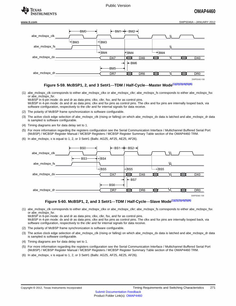
abe_mcbspx_clk
abe_mcbspx_fs
abe_mcbspx_dx
abe_mcbspx_dr
DX7 DX6 DX0
DR7 DR6 DR0
BM3 BM3
BM4
BM0 BM1 BM2
BM5
BM6
BM4 BM4
SWPS040-108
abe_mcbspx_clk
abe_mcbspx_fs
abe_mcbspx_dx
abe_mcbspx_dr
DX7 DX6 DX0
DR7 DR6 DR0
BS4
BS5
BS0 BS1 BS2
BS6
BS7
BS5 BS5
BS3
SWPS040-109
Public Version
OMAP4460
www.ti.com SWPS046A –JANUARY 2012
Figure 5-59. McBSP1, 2, and 3 Set#1—TDM / Half-Cycle—Master Mode(1)(2)(3)(4)(5)(6)
(1) abe_mcbspx_clk corresponds to either abe_mcbspx_clkx or abe_mcbspx_clkr; abe_mcbspx_fs corresponds to either abe_mcbspx_fsxor abe_mcbspx_fsr.McBSP in 6-pin mode: dx and dr as data pins; clkx, clkr, fsx, and fsr as control pins.McBSP in 4-pin mode: dx and dr as data pins; clkx and fsx pins as control pins. The clkx and fsx pins are internally looped back, viasoftware configuration, respectively to the clkr and fsr internal signals for data receive.
(2) The polarity of McBSP frame synchronization is software configurable.
(3) The active clock edge selection of abe_mcbspx_clk (rising or falling) on which abe_mcbspx_dx data is latched and abe_mcbspx_dr datais sampled is software configurable.
(4) Timing diagrams are for data delay set to 1.
(5) For more information regarding the registers configuration see the Serial Communication Interface / Multichannel Buffered Serial Port(McBSP) / MCBSP Register Manual / MCBSP Registers / MCBSP Register Summary Table section of the OMAP4460 TRM.
(6) In abe_mcbspx, x is equal to 1, 2, or 3 Set#1 (Balls: AG25, AF25, AE25, AF26).
Figure 5-60. McBSP1, 2, and 3 Set#1—TDM / Half-Cycle—Slave Mode(1)(2)(3)(4)(5)(6)
(1) abe_mcbspx_clk corresponds to either abe_mcbspx_clkx or abe_mcbspx_clkr; abe_mcbspx_fs corresponds to either abe_mcbspx_fsxor abe_mcbspx_fsr.McBSP in 6-pin mode: dx and dr as data pins; clkx, clkr, fsx, and fsr as control pins.McBSP in 4-pin mode: dx and dr as data pins; clkx and fsx pins as control pins. The clkx and fsx pins are internally looped back, viasoftware configuration, respectively to the clkr and fsr internal signals for data receive.
(2) The polarity of McBSP frame synchronization is software configurable.
(3) The active clock edge selection of abe_mcbspx_clk (rising or falling) on which abe_mcbspx_dx data is latched and abe_mcbspx_dr datais sampled is software configurable.
(4) Timing diagrams are for data delay set to 1.
(5) For more information regarding the registers configuration see the Serial Communication Interface / Multichannel Buffered Serial Port(McBSP) / MCBSP Register Manual / MCBSP Registers / MCBSP Register Summary Table section of the OMAP4460 TRM.
(6) In abe_mcbspx, x is equal to 1, 2, or 3 Set#1 (Balls: AG25, AF25, AE25, AF26).
Copyright © 2012, Texas Instruments Incorporated Timing Requirements and Switching Characteristics 271Submit Documentation Feedback
Product Folder Link(s): OMAP4460

Public Version
OMAP4460
SWPS046A –JANUARY 2012 www.ti.com
5.6.1.1.2.2 McBSP1, McBSP2, and McBSP3 Set#1—TDM / Half-Cycle—12MHz, 5-pF Load Capacitance
Table 5-52 through Table 5-55 assume testing over the recommended operating conditions and electricalcharacteristic conditions below (see Figure 5-61 and Figure 5-62).
Table 5-51. McBSP1, McBSP2, and McBSP3 Set#1 Timing Conditions—TDM / Half-Cycle(1)(2)(3)
SYSTEM CONDITION PARAMETER VALUE UNIT
MIN MAX
Input Conditions
tR Input signal rise time 600 6500 ps
tF Input signal fall time 600 6500 ps
PCB Conditions
Number of external peripherals 1
Far end load 5 pF
Trace length 9 cm
Characteristics impedance 20 60 Ω
(1) IO settings: MB[1:0] = 10 and LB0 = 0 McBSP3 Set#1 means the following balls: AG25, AF25, AE25, AF26.For more information, see Control Module / Control Module Functional Description/ Functional Register Description / Signal IntegrityParameter Control Registers with Pad Group Assignment / 50-Ω Output Buffer I/Os with Combined Mode and Load Settings section ofthe OMAP4460 TRM.
(2) In this table the rise and fall times are calculated for 10% to 90% of VDDS. For more information on the corresponding OMAP4 VDDSpower supply name, see Table 2-1, POWER [9] column with the ball name.
(3) To have an idea of the output OMAP4 ball load supported for this application, you can consider the following:Output OMAP4 ball load = Far End load + 1.34 pF/cm typical x trace length (cm).
5.6.1.1.2.2.1 McBSP1, McBSP2, and McBSP3 Set#1—TDM / Half-Cycle—Master Mode
Table 5-52. McBSP1, McBSP2, and McBSP3 Set#1 Timing Requirements—TDM / Half-Cycle—MasterMode(1)(3)(6)
NO. PARAMETER OPP100, OPP119 OPP50 UNIT
MIN MAX MIN MAX
1 / tc(clks) Frequency, input abe_clks(5) clock 12.288(5) 6.144(5) MHz
tw(clksL) Typical pulse duration, input abe_clks low 0.5 * P(4) 0.5 * P(4) ns
tw(clksH) Typical pulse duration, output abe_clks high 0.5 * P(4) 0.5 * P(4) ns
tdc(clks) Duty cycle error, input abe_clks –0.05 * 0.05 * –0.05 * 0.05 * psP(4) + 610 P(4) – 610 P(4) + 610 P(4) – 610
tj(clks) Jitter peak to peak, input abe_clks 300 300 ps
BM5 tsu(drV-clkAE) Setup time, abe_mcbspx_dr valid before 11.3 24.3 nsabe_mcbspx_clk(2) active edge
BM6 th(clkAE-drV) Hold time, abe_mcbspx_dr valid after –2.4 –2.4 nsabe_mcbspx_clk(2) active edge
(1) The timings apply to all configurations regardless of abe_mcbspx_clk polarity and which clock edges are used to drive output data andcapture input data.
(2) abe_mcbspx_clk corresponds to either abe_mcbspx_clkx or abe_mcbspx_clkr; abe_mcbspx_clkr is available in 6-pin mode only.
(3) In abe_mcbspx, x is equal to 1, or 2, or 3 Set#1 (Balls: AG25, AF25, AE25, AF26).
(4) P = abe_clks input clock period in ns
(5) The McPDM interface can be used at the same time with one or more McBSP (interface 1, 2, or 3). In this case, abe_clks clock isshared, that means identical, between McPDM and McBSP. As a consequence, the minimum clock frequency between McPDM andMcBSP, input jitter, and duty cycle must be considered between both interfaces.
(6) See DM Operating Condition Addendum for CORE OPP voltages.
Table 5-53. McBSP1, McBSP2, and McBSP3 Set#1 Switching Characteristics—TDM / Half-Cycle—Master
272 Timing Requirements and Switching Characteristics Copyright © 2012, Texas Instruments Incorporated
Submit Documentation FeedbackProduct Folder Link(s): OMAP4460

Public Version
OMAP4460
www.ti.com SWPS046A –JANUARY 2012
Table 5-53. McBSP1, McBSP2, and McBSP3 Set#1 Switching Characteristics—TDM / Half-Cycle—MasterMode(4)(7)(9) (continued)
Mode(4)(7)(9)
NO. PARAMETER OPP100, OPP119 OPP50 UNIT
MIN MAX MIN MAX
BM0 1 / tc(clk) Frequency(1), output abe_mcbspx_clk(5) clock 12.288(8) 6.144(8) MHz
BM1 tw(clkL) Typical Pulse duration, output 0.5*P(2) 0.5*P(2) nsabe_mcbspx_clk(5) low
BM2 tw(clkH) Typical Pulse duration, output 0.5*P(2) 0.5*P(2) nsabe_mcbspx_clk(5) high
tdc(clk) Duty cycle error, output abe_mcbspx_clk(5) –4069 4069 –8138 8138 ps
tJ(clk) Jitter standard deviation(3), output 65 65 psabe_mcbspx_clk(5)
tR(clk) Rise time, output abe_mcbspx_clk(5) 600 6500 600 6500 ps
tF(clk) Fall time, output abe_mcbspx_clk(5) 600 6500 600 6500 ps
BM3 td(clkAE-fsV) Delay time, output abe_mcbspx_clk(5) active –14.6 22.4 –30.9 46.4 nsedge to output abe_mcbspx_fs(6) valid
BM4 td(clkxAE-dxV) Delay time, output abe_mcbspx_clkx active –14.6 22.4 –30.9 46.4 nsedge to output abe_mcbspx_dx valid
tR(fs) Rise time, output abe_mcbspx_fs(6) 600 6500 600 6500 ps
tF(fs) Fall time, output abe_mcbspx_fs(6) 600 6500 600 6500 ps
tR(dx) Rise time, output abe_mcbspx_dx 600 6500 600 6500 ps
tF(dx) Fall time, output abe_mcbspx_dx 600 6500 600 6500 ps
(1) Related to the output abe_mcbspx_clkx / abe_mcbspx_clkr maximum and minimum frequency programmable in McBSP module bysetting the configuration register SRGR1_REG[7..0].For more information regarding the registers configuration see Serial Communication Interface / Multichannel Buffered Serial Port(McBSP) MCBSP Register Manual / MCBSP Registers / MCBSP Register Summary Table section of the OMAP4460 TRM.
(2) P = abe_mcbspx_clkx / abe_mcbspx_clkr output clk period in ns
(3) The jitter probability density can be approximated by a Gaussian function.
(4) The timings apply to all configurations regardless of abe_mcbsp_clk polarity and which clock edges are used to drive output data andcapture input data.
(5) abe_mcbspx_clk corresponds to either abe_mcbspx_clkx or abe_mcbspx_clkr; abe_mcbspx_clkr is available in 6-pin mode only.
(6) abe_mcbspx_fs corresponds to either abe_mcbspx_fsx or abe_mcbspx_fsr; abe_mcbspx_fsr is available in 6-pin mode only.
(7) In abe_mcbspx, x is equal to 1 or, 2 or, 3 Set#1 (Balls: AG25, AF25, AE25, AF26).
(8) This McBSP1, 2 output clock frequency is based on an output ABE DPLL configured at 196.608 MHz.For more information regarding the registers configuration, see Power, Reset and Clock Management / Clock Management FunctionalDescription / Internal Clock Sources/Generators / DPLL_ABE Description section of the OMAP4460 TRM.
(9) See DM Operating Condition Addendum for CORE OPP voltages.
5.6.1.1.2.2.2 McBSP1, McBSP2, and McBSP3 Set#1—TDM / Half-Cycle—Slave Mode
Table 5-54. McBSP1, McBSP2, and McBSP3 Set#1 Timing Requirements—TDM / Half-Cycle—SlaveMode(5)(8)(9)
NO. PARAMETER OPP100, OPP119 OPP50 UNIT
MIN MAX MIN MAX
BS0 1 / tc(clk) Frequency(1), abe_mcbspx_clk(6) 12.288 6.144 MHz
BS1 tw(clkL) Typical Pulse duration, abe_mcbspx_clk(6) low 0.5*P(2) 0.5*P(2) ns
BS2 tw(clkH) Typical Pulse duration, abe_mcbspx_clk(6) 0.5*P(2) 0.5*P(2) nshigh
tdc(clk) Duty cycle error, abe_mcbspx_clk(6) –4069 4069 –8138 8138 ps
tJ(clk) Cycle jitter(3), abe_mcbspx_clk(6) 2000 2000 ps
BS3 tsu(fsV-clkAE) Setup time, abe_mcbspx_fs(7) valid before 11.9 26.5 nsabe_mcbspx_clk(6) active edge
Copyright © 2012, Texas Instruments Incorporated Timing Requirements and Switching Characteristics 273Submit Documentation Feedback
Product Folder Link(s): OMAP4460
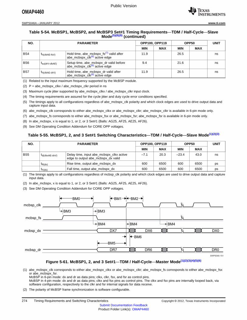
mcbsp_clk
mcbsp_fs
mcbsp_dx
mcbsp_dr
DX7 DX6 DX0
DR7 DR6 DR0
BM3 BM3
BM4
BM0 BM1 BM2
BM5
BM6
BM4 BM4
SWPS040-151
Public Version
OMAP4460
SWPS046A –JANUARY 2012 www.ti.com
Table 5-54. McBSP1, McBSP2, and McBSP3 Set#1 Timing Requirements—TDM / Half-Cycle—SlaveMode(5)(8)(9) (continued)
NO. PARAMETER OPP100, OPP119 OPP50 UNIT
MIN MAX MIN MAX
BS4 th(clkAE-fsV) Hold time, abe_mcbspx_fs(7) valid after 11.9 26.5 nsabe_mcbspx_clk(6) active edge
BS6 tsu(drV-clkAE) Setup time, abe_mcbspx_dr valid before 9.4 21.6 nsabe_mcbspx_clk(6) active edge
BS7 th(clkAE-drV) Hold time, abe_mcbspx_dr valid after 11.9 26.5 nsabe_mcbspx_clk(6) active edge
(1) Related to the input maximum frequency supported by the McBSP module.
(2) P = abe_mcbspx_clkx / abe_mcbspx_clkr period in ns
(3) Maximum cycle jitter supported by abe_mcbspx_clkx / abe_mcbspx_clkr input clock.
(4) The timing requirements are assured for the cycle jitter and duty cycle error conditions specified.
(5) The timings apply to all configurations regardless of abe_mcbspx_clk polarity and which clock edges are used to drive output data andcapture input data.
(6) abe_mcbspx_clk corresponds to either abe_mcbspx_clkx or abe_mcbspx_clkr; abe_mcbspx_clkr is available in 6-pin mode only.
(7) abe_mcbspx_fs corresponds to either abe_mcbspx_fsx or abe_mcbspx_fsr; abe_mcbspx_fsr is available in 6-pin mode only.
(8) In abe_mcbspx, x is equal to 1, or 2, or 3 Set#1 (Balls: AG25, AF25, AE25, AF26).
(9) See DM Operating Condition Addendum for CORE OPP voltages.
Table 5-55. McBSP1, 2, and 3 Set#1 Switching Characteristics—TDM / Half-Cycle—Slave Mode(1)(2)(3)
NO. PARAMETER OPP100, OPP119 OPP50 UNIT
MIN MAX MIN MAX
BS5 td(clkxAE-dxV) Delay time, input abe_mcbspx_clkx active –7.1 20.3 –23.4 43.0 nsedge to output abe_mcbspx_dx valid
tR(dx) Rise time, output abe_mcbspx_dx 600 6500 600 6500 ps
tF(dx) Fall time, output abe_mcbspx_dx 600 6500 600 6500 ps
(1) The timings apply to all configurations regardless of mcbsp_clk polarity and which clock edges are used to drive output data and captureinput data.
(2) In abe_mcbspx, x is equal to 1, or 2, or 3 Set#1 (Balls: AG25, AF25, AE25, AF26).
(3) See DM Operating Condition Addendum for CORE OPP voltages.
Figure 5-61. McBSP1, 2, and 3 Set#1—TDM / Half-Cycle—Master Mode(1)(2)(3)(4)(5)(6)
(1) abe_mcbspx_clk corresponds to either abe_mcbspx_clkx or abe_mcbspx_clkr; abe_mcbspx_fs corresponds to either abe_mcbspx_fsxor abe_mcbspx_fsr.McBSP in 6-pin mode: dx and dr as data pins; clkx, clkr, fsx, and fsr as control pins.McBSP in 4-pin mode: dx and dr as data pins; clkx and fsx pins as control pins. The clkx and fsx pins are internally looped back, viasoftware configuration, respectively to the clkr and fsr internal signals for data receive.
(2) The polarity of McBSP frame synchronization is software configurable.
274 Timing Requirements and Switching Characteristics Copyright © 2012, Texas Instruments Incorporated
Submit Documentation FeedbackProduct Folder Link(s): OMAP4460

mcbsp_clk
mcbsp_fs
mcbsp_dx
mcbsp_dr
DX7 DX6 DX0
DR7 DR6 DR0
BS3 BS4
BS5
BS0 BS1 BS2
BS6
BS7
BS5 BS5
SWPS040-152
Public Version
OMAP4460
www.ti.com SWPS046A –JANUARY 2012
(3) The active clock edge selection of abe_mcbspx_clk (rising or falling) on which abe_mcbspx_dx data is latched and abe_mcbspx_dr datais sampled is software configurable.
(4) Timing diagrams are for data delay set to 1.
(5) For more information regarding the registers configuration see Serial Communication Interface / Multichannel Buffered Serial Port(McBSP) MCBSP Register Manual / MCBSP Registers / MCBSP Register Summary Table section of the OMAP4460 TRM.
(6) In abe_mcbspx, x is equal to 1, or 2, or 3 Set#1 (Balls: AG25, AF25, AE25, AF26).
Figure 5-62. McBSP1, 2, and 3 Set#1—TDM / Half-Cycle—Slave Mode(1)(2)(3)(4)(5)(6)
(1) abe_mcbspx_clk corresponds to either abe_mcbspx_clkx or abe_mcbspx_clkr; abe_mcbspx_fs corresponds to either abe_mcbspx_fsxor abe_mcbspx_fsr.McBSP in 6-pin mode: dx and dr as data pins; clkx, clkr, fsx, and fsr as control pins.McBSP in 4-pin mode: dx and dr as data pins; clkx and fsx pins as control pins. The clkx and fsx pins are internally looped back, viasoftware configuration, respectively to the clkr and fsr internal signals for data receive.
(2) The polarity of McBSP frame synchronization is software configurable.
(3) The active clock edge selection of abe_mcbspx_clk (rising or falling) on which abe_mcbspx_dx data is latched and abe_mcbspx_dr datais sampled is software configurable.
(4) Timing diagrams are for data delay set to 1.
(5) For more information regarding the registers configuration see Serial Communication Interface / Multichannel Buffered Serial Port(McBSP) MCBSP Register Manual / MCBSP Registers / MCBSP Register Summary Table section of the OMAP4460 TRM.
(6) In abe_mcbspx, x is equal to 1, or 2, or 3 Set#1 (Balls: AG25, AF25, AE25, AF26).
5.6.1.2 McBSP3—I2S/PCM
Table 5-57 through Table 5-60 assume testing over the recommended operating conditions and electricalcharacteristic conditions below (see Figure 5-63 and Figure 5-64).
Table 5-56. McBSP3 Timing Conditions—I2S/PCM(1)(2)(3)
SYSTEM CONDITION PARAMETER VALUE UNIT
MIN MAX
Input Conditions
tR Input signal rise time 400 6500 ps
tF Input signal fall time 400 6500 ps
PCB Conditions
Bottom Balls: AG25 / AF25 / AE25 / AF26
Number of external peripherals 1
Far end load 5 pF
Trace length, point-to-point interconnect 9 cm
Characteristics impedance 30 55 ΩBottom Balls: AH17 / AE16 / AF16 / AG16
Number of external peripherals 1
Far end load 5 pF
Copyright © 2012, Texas Instruments Incorporated Timing Requirements and Switching Characteristics 275Submit Documentation Feedback
Product Folder Link(s): OMAP4460

Public Version
OMAP4460
SWPS046A –JANUARY 2012 www.ti.com
Table 5-56. McBSP3 Timing Conditions—I2S/PCM(1)(2)(3) (continued)
SYSTEM CONDITION PARAMETER VALUE UNIT
MIN MAX
Trace length, point-to-point interconnect 9 cm
Characteristics impedance 30 45 Ω
(1) IO settings: MB[1:0] = 10 and LB0 = 0.For more information, see:
– For balls AG25 / AF25 / AE25 / AF26, Control Module / Control Module Functional Description/ Functional Register Description /Signal Integrity Parameter Control Registers with Pad Group Assignment / 50-Ω Output Buffer I/Os with Combined Mode and LoadSettings section of the OMAP4460 TRM
– For balls AH17 / AE16 / AF16 / AG16, Control Module / Control Module Functional Description/ Functional Register Description /Signal Integrity Parameter Control Registers with Pad Group Assignment / I/Os with Combined Mode and Load Settings section ofthe OMAP4460 TRM.
(2) In this table the rise and fall times are calculated for 10% to 90% of VDDS. For more information on the corresponding OMAP4 VDDSpower supply name, see Table 2-1, POWER [9] column with the ball name.
(3) To have an idea of the output OMAP4 ball load supported for this application, you can consider the following:Output OMAP4 ball load = Far End load + 1.34 pF/cm typical x trace length (cm).
5.6.1.2.1 McBSP3—I2S/PCM Full and Half Cycle—Master Mode—24 MHz
Table 5-57. McBSP3 Timing Requirements—I2S/PCM—Master Mode(1)(5)
NO. PARAMETER OPP100, OPP119 OPP50 UNIT
MIN MAX MIN MAX
1 / tc(clks) Frequency, input abe_clks(4) clock 24.576(4) 12.288(4) MHz
tw(clksL) Typical pulse duration, input abe_clks low 0.5 * P(3) 0.5 * P(3) ns
tw(clksH) Typical pulse duration, output abe_clks high 0.5 * P(3) 0.5 * P(3) ns
tdc(clks) Duty cycle error, input abe_clks –0.05 * 0.05 * –0.05 * 0.05 * psP(3) + 610 P(3) – 610 P(3) + 610 P(3) – 610
tj(clks) Jitter peak to peak, input abe_clks 300 300 ps
For balls: AH17 / AE16 / AF16 / AG16 (abe_mcbsp3_dr / abe_mcbsp3_dx / abe_mcbsp3_clkx / abe_mcbsp3_fsx)—Multiplexingmode 2
BM5 tsu(drV-clkAE) Setup time, abe_mcbsp3_dr valid before 5.6 11.5 nsabe_mcbsp3_clk(2) active edge
BM6 th(clkAE-drV) Hold time, abe_mcbsp3_dr valid after 0.8 0.7 nsabe_mcbsp3_clk(2) active edge
For balls: AG25 / AF25 / AE25 / AF26 (abe_mcbsp3_dr / abe_mcbsp3_dx / abe_mcbsp3_clkx / abe_mcbsp3_fsx)—Multiplexingmode 1
BM5 tsu(drV-clkAE) Setup time, abe_mcbsp3_dr valid before 4.6 10.5 nsabe_mcbsp3_clk(2) active edge
BM6 th(clkAE-drV) Hold time, abe_mcbsp3_dr valid after 0.7 0.6 nsabe_mcbsp3_clk(2) active edge
(1) The timings apply to all configurations regardless of abe_mcbsp3_clk polarity and which clock edges are used to drive output data andcapture input data.
(2) abe_mcbsp3_clk corresponds to either abe_mcbsp3_clkx or abe_mcbsp3_clkr; abe_mcbsp3_clkr is available in 6-pin mode only.
(3) P = abe_clks input clock period in ns
(4) The McPDM interface can be used at the same time with one or more McBSP (interface 1, 2, or 3). In this case, abe_clks clock isshared, that means identical, between McPDM and McBSP. As a consequence, the minimum clock frequency between McPDM andMcBSP, input jitter, and duty cycle must be considered between both interfaces.
(5) See DM Operating Condition Addendum for CORE OPP voltages.
Table 5-58. McBSP3 Switching Characteristics—I2S/PCM—Master Mode(4)(8)
NO. PARAMETER OPP100, OPP119 OPP50 UNIT
MIN MAX MIN MAX
For balls: AE16 / AF16 / AG16 (abe_mcbsp3_dx / abe_mcbsp3_clkx / abe_mcbsp3_fsx)—Multiplexing mode 2
BM0 1 / tc(clk) Frequency(1), output abe_mcbsp3_clk(5) clock 24.576(7) 12.288(7) MHz
276 Timing Requirements and Switching Characteristics Copyright © 2012, Texas Instruments Incorporated
Submit Documentation FeedbackProduct Folder Link(s): OMAP4460
Public Version
OMAP4460
www.ti.com SWPS046A –JANUARY 2012
Table 5-58. McBSP3 Switching Characteristics—I2S/PCM—Master Mode(4)(8) (continued)
NO. PARAMETER OPP100, OPP119 OPP50 UNIT
MIN MAX MIN MAX
BM1 tw(clkL) Typical pulse duration, output abe_mcbsp3_clk(5) low 0.5*P(2) 0.5*P(2) ns
BM2 tw(clkH) Typical pulse duration, output abe_mcbsp3_clk(5) high 0.5*P(2) 0.5*P(2) ns
tdc(clk) Duty cycle error, output abe_mcbsp3_clk(5) –2035 2035 –4069 4069 ps
tj(clk) Jitter standard deviation(3), output abe_mcbsp3_clk(5) 65 65 ps
tR(clk) Rise time, output abe_mcbsp3_clk(5) 400 6500 400 6500 ps
tF(clk) Fall time, output abe_mcbsp3_clk(5) 400 6500 400 6500 ps
BM3 td(clkAE-fsV) Delay time, output abe_mcbsp3_clk(5) active edge to 0.9 11.4 1.1 23.1 nsoutput abe_mcbsp3_fs(6) valid
BM4 td(clkxAE-dxV) Delay time, output abe_mcbsp3_clkx active edge to 0.9 11.4 1.1 23.1 nsoutput abe_mcbsp3_dx valid
tR(fs) Rise time, output abe_mcbsp3_fs(6) 400 6500 400 6500 ps
tF(fs) Fall time, output abe_mcbsp3_fs(6) 400 6500 400 6500 ps
tR(dx) Rise time, output abe_mcbsp3_dx 400 6500 400 6500 ps
tF(dx) Fall time, output abe_mcbsp3_dx 400 6500 400 6500 ps
Copyright © 2012, Texas Instruments Incorporated Timing Requirements and Switching Characteristics 277Submit Documentation Feedback
Product Folder Link(s): OMAP4460

Public Version
OMAP4460
SWPS046A –JANUARY 2012 www.ti.com
Table 5-58. McBSP3 Switching Characteristics—I2S/PCM—Master Mode(4)(8) (continued)
NO. PARAMETER OPP100, OPP119 OPP50 UNIT
MIN MAX MIN MAX
For balls: AF25 / AE25 / AF26 (abe_mcbsp3_dx / abe_mcbsp3_clkx / abe_mcbsp3_fsx)—Multiplexing mode 1
BM0 1 / tc(clk) Frequency(1), output abe_mcbsp3_clk(5) clock 24.576(7) 12.288(7) MHz
BM1 tw(clkL) Typical pulse duration, output abe_mcbsp3_clk(5) low 0.5*P(2) 0.5*P(2) ns
BM2 tw(clkH) Typical pulse duration, output abe_mcbsp3_clk(5) high 0.5*P(2) 0.5*P(2) ns
tdc(clk) Duty cycle error, output abe_mcbsp3_clk(5) –2035 2035 –4069 4069 ps
tj(clk) Jitter standard deviation(3), output abe_mcbsp3_clk(5) 65 65 ps
tR(clk) Rise time, output abe_mcbsp3_clk(5) 400 6500 400 6500 ps
tF(clk) Fall time, output abe_mcbsp3_clk(5) 400 6500 400 6500 ps
BM3 td(clkAE-fsV) Delay time, output abe_mcbsp3_clk(5) active edge to 0.9 11.0 1.0 22.6 nsoutput abe_mcbsp3_fs(6) valid
BM4 td(clkxAE-dxV) Delay time, output abe_mcbsp3_clkx active edge to 0.9 11.0 1.0 22.6 nsoutput abe_mcbsp3_dx valid
tR(fs) Rise time, output abe_mcbsp3_fs(6) 400 6500 400 6500 ps
tF(fs) Fall time, output abe_mcbsp3_fs(6) 400 6500 400 6500 ps
tR(dx) Rise time, output abe_mcbsp3_dx 400 6500 400 6500 ps
tF(dx) Fall time, output abe_mcbsp3_dx 400 6500 400 6500 ps
(1) Related to the output abe_mcbsp3_clkx / abe_mcbsp3_clkr maximum and minimum frequency programmable in McBSP module bysetting the configuration register SRGR1_REG[7..0].For more information regarding the registers configuration see the Serial Communication Interface / Multichannel Buffered Serial Port(McBSP) / MCBSP Register Manual / MCBSP Registers / MCBSP Register Summary Table section of the OMAP4460 TRM.
(2) P = abe_mcbsp3_clkx / abe_mcbsp3_clkr output clk period in ns
(3) The jitter probability density can be approximated by a Gaussian function.
(4) The timings apply to all configurations regardless of abe_mcbsp3_clk polarity and which clock edges are used to drive output data andcapture input data.
(5) abe_mcbsp3_clk corresponds to either abe_mcbsp3_clkx or abe_mcbsp3_clkr; abe_mcbsp3_clkr is available in 6-pin mode only.
(6) abe_mcbsp3_fs corresponds to either abe_mcbsp3_fsx or abe_mcbsp3_fsr; abe_mcbsp3_fsr is available in 6-pin mode only.
(7) This McBSP3 output clock frequency is based on an output ABE DPLL configured at 196.608 MHz.For more information regarding the registers configuration, see the Power, Reset and Clock Management / Clock ManagementFunctional Description / Internal Clock Sources/Generators / DPLL_ABE Description section of the OMAP4460 TRM
(8) See DM Operating Condition Addendum for CORE OPP voltages.
5.6.1.2.2 McBSP3—I2S/PCM Full and Half Cycle—Slave Mode—12 MHz
Table 5-59. McBSP3 Timing Requirements—I2S/PCM—Slave Mode(4)(5)(8)
NO. PARAMETER OPP100, OPP119 OPP50 UNIT
MIN MAX MIN MAX
For balls: AH17 / AE16 / AF16 / AG16 (abe_mcbsp3_dr / abe_mcbsp3_dx / abe_mcbsp3_clkx / abe_mcbsp3_fsx)—Multiplexingmode 2
BS0 1 / tc(clk) Frequency(1), abe_mcbsp3_clk(6) 12.288 6.144 MHz
BS1 tw(clkL) Typical pulse duration, abe_mcbsp3_clk(6) low 0.5*P(2) 0.5*P(2) ns
BS2 tw(clkH) Typical pulse duration, abe_mcbsp3_clk(6) high 0.5*P(2) 0.5*P(2) ns
tdc(clk) Duty cycle error, abe_mcbsp3_clk(6) –2035 2035 –4069 4069 ps
tj(clk) Cycle jitter(3), abe_mcbsp3_clk(6) 1221 2000 ps
BS3 tsu(fsV-clkAE) Setup time, abe_mcbsp3_fs(7) valid before 14.8 30.8 nsabe_mcbsp3_clk(6) active edge
BS4 th(clkAE-fsV) Hold time, abe_mcbsp3_fs(7) valid after 14.8 30.8 nsabe_mcbsp3_clk(6) active edge
BS6 tsu(drV-clkAE) Setup time, abe_mcbsp3_dr valid before 14.8 30.8 nsabe_mcbsp3_clk(6) active edge
BS7 th(clkAE-drV) Hold time, abe_mcbsp3_dr valid after 14.8 30.8 nsabe_mcbsp3_clk(6) active edge
278 Timing Requirements and Switching Characteristics Copyright © 2012, Texas Instruments Incorporated
Submit Documentation FeedbackProduct Folder Link(s): OMAP4460
Public Version
OMAP4460
www.ti.com SWPS046A –JANUARY 2012
Table 5-59. McBSP3 Timing Requirements—I2S/PCM—Slave Mode(4)(5)(8) (continued)
NO. PARAMETER OPP100, OPP119 OPP50 UNIT
MIN MAX MIN MAX
For balls: AG25 / AF25 / AE25 / AF26 (abe_mcbsp3_dr / abe_mcbsp3_dx / abe_mcbsp3_clkx / abe_mcbsp3_fsx)—Multiplexingmode 1
BS0 1 / tc(clk) Frequency(1), abe_mcbsp3_clk(6) 12.288 6.144 MHz
BS1 tw(clkL) Typical pulse duration, abe_mcbsp3_clk(6) low 0.5*P(2) 0.5*P(2) ns
BS2 tw(clkH) Typical pulse duration, abe_mcbsp3_clk(6) high 0.5*P(2) 0.5*P(2) ns
tdc(clk) Duty cycle error, abe_mcbsp3_clk(6) –2035 2035 –4069 4069 ps
tj(clk) Cycle jitter(3), abe_mcbsp3_clk(6) 1221 2000 ps
BS3 tsu(fsV-clkAE) Setup time, abe_mcbsp3_fs(7) valid before 14.3 30.4 nsabe_mcbsp3_clk(6) active edge
BS4 th(clkAE-fsV) Hold time, abe_mcbsp3_fs(7) valid after 14.3 30.4 nsabe_mcbsp3_clk(6) active edge
BS6 tsu(drV-clkAE) Setup time, abe_mcbsp3_dr valid before 14.3 30.4 nsabe_mcbsp3_clk(6) active edge
BS7 th(clkAE-drV) Hold time, abe_mcbsp3_dr valid after 14.3 30.4 nsabe_mcbsp3_clk(6) active edge
(1) Related to the input maximum frequency supported by the McBSP module.
(2) P = abe_mcbsp3_clkx / abe_mcbsp3_clkr period in ns
(3) Maximum cycle jitter supported by abe_mcbsp3_clkx / abe_mcbsp3_clkr input clock.
(4) The timing requirements are assured for the cycle jitter and duty cycle error conditions specified.
(5) The timings apply to all configurations regardless of abe_mcbsp3_clk polarity and which clock edges are used to drive output data andcapture input data.
(6) abe_mcbsp3_clk corresponds to either abe_mcbsp3_clkx or abe_mcbsp3_clkr; abe_mcbsp3_clkr is available in 6-pin mode only.
(7) abe_mcbsp3_fs corresponds to either abe_mcbsp3_fsx or abe_mcbsp3_fsr; abe_mcbsp3_fsr is available in 6-pin mode only.
(8) See DM Operating Condition Addendum for CORE OPP voltages.
Table 5-60. McBSP3 Switching Characteristics—I2S/PCM—Slave Mode(1)(2)
NO. PARAMETER OPP100, OPP119 OPP50 UNIT
MIN MAX MIN MAX
For balls: AE16 / AF16 / AG16 (abe_mcbsp3_dx / abe_mcbsp3_clkx / abe_mcbsp3_fsx)—Multiplexing mode 2
BS5 td(clkxAE-dxV) Delay time, input abe_mcbsp3_clkx active –16.4 22.3 –34.1 38.1 nsedge to output abe_mcbsp3_dx valid
tR(dx) Rise time, output abe_mcbsp3_dx 400 6500 400 6500 ps
tF(dx) Fall time, output abe_mcbsp3_dx 400 6500 400 6500 ps
For balls: AF25 / AE25 / AF26 (abe_mcbsp3_dx / abe_mcbsp3_clkx / abe_mcbsp3_fsx)—Multiplexing mode 1
BS5 td(clkxAE-dxV) Delay time, input abe_mcbsp3_clkx active –16.4 20.3 –34.0 36.1 nsedge to output abe_mcbsp3_dx valid
tR(dx) Rise time, output abe_mcbsp3_dx 400 6500 400 6500 ps
tF(dx) Fall time, output abe_mcbsp3_dx 400 6500 400 6500 ps
(1) The timings apply to all configurations regardless of abe_mcbsp3_clk polarity and which clock edges are used to drive output data andcapture input data.
(2) See DM Operating Condition Addendum for CORE OPP voltages.
Copyright © 2012, Texas Instruments Incorporated Timing Requirements and Switching Characteristics 279Submit Documentation Feedback
Product Folder Link(s): OMAP4460

abe_mcbsp3_clk
abe_mcbsp3_fs
abe_mcbsp3_dx
abe_mcbsp3_dr
DX7 DX6 DX0
DR7 DR6 DR0
BM3 BM3
BM4
BM0 BM1 BM2
BM5
BM6
SWPS040-117
BM4 BM4
abe_mcbsp3_clk
abe_mcbsp3_fs
abe_mcbsp3_dx
abe_mcbsp3_dr
DX7 DX6 DX0
DR7 DR6 DR0
BS4
BS5
BS0 BS1 BS2
BS6
BS7
BS5 BS5
BS3
SWPS040-118
Public Version
OMAP4460
SWPS046A –JANUARY 2012 www.ti.com
Figure 5-63. McBSP3—I2S/PCM—Master Mode(1)(2)(3)(4)(5)
(1) abe_mcbsp3_clk corresponds to either abe_mcbsp3_clkx or abe_mcbsp3_clkr; abe_mcbsp3_fs corresponds to either abe_mcbsp3_fsxor abe_mcbsp3_fsr.McBSP in 6-pin mode: dx and dr as data pins; clkx, clkr, fsx, and fsr as control pins.McBSP in 4-pin mode: dx and dr as data pins; clkx and fsx pins as control pins. The clkx and fsx pins are internally looped back, viasoftware configuration, respectively to the clkr and fsr internal signals for data receive.
(2) The polarity of McBSP frame synchronization is software configurable.
(3) The active clock edge selection of abe_mcbsp3_clk (rising or falling) on which abe_mcbsp3_dx data is latched and abe_mcbsp3_drdata is sampled is software configurable.
(4) Timing diagrams are for data delay set to 1.
(5) For more information regarding the registers configuration see the Serial Communication Interface / Multichannel Buffered Serial Port(McBSP) MCBSP Register Manual / MCBSP Registers / MCBSP Register Summary Table section of the OMAP4460 TRM.
Figure 5-64. McBSP3—I2S/PCM—Slave Mode(1)(2)(3)(4)(5)
(1) mcbsp3_clk corresponds to either mcbsp3_clkx or mcbsp3_clkr; mcbsp3_fs corresponds to either mcbsp3_fsx or mcbsp3_fsr.McBSP in 6-pin mode: dx and dr as data pins; clkx, clkr, fsx, and fsr as control pins.McBSP in 4-pin mode: dx and dr as data pins; clkx and fsx pins as control pins. The clkx and fsx pins are internally looped back, viasoftware configuration, respectively to the clkr and fsr internal signals for data receive.
(2) The polarity of McBSP frame synchronization is software configurable.
(3) The active clock edge selection of mcbsp3_clk (rising or falling) on which mcbsp3_dx data is latched and mcbsp3_dr data is sampled issoftware configurable.
(4) Timing diagrams are for data delay set to 1.
(5) For more information regarding the registers configuration see the Serial Communication Interface / Multichannel Buffered Serial Port(McBSP) MCBSP Register Manual / MCBSP Registers / MCBSP Register Summary Table section of the OMAP4460 TRM.
280 Timing Requirements and Switching Characteristics Copyright © 2012, Texas Instruments Incorporated
Submit Documentation FeedbackProduct Folder Link(s): OMAP4460

Public Version
OMAP4460
www.ti.com SWPS046A –JANUARY 2012
5.6.1.3 McBSP4—I2S/PCM
5.6.1.3.1 McBSP4—I2S/PCM—Full Cycle—48-MHz Master and 24-MHz Slave
Table 5-62 through Table 5-65 assume testing over the recommended operating conditions and electricalcharacteristic conditions below (see Figure 5-65 and Figure 5-66).
Table 5-61. McBSP4 Timing Conditions—I2S/PCM(1)(2)(3)
SYSTEM CONDITION PARAMETER VALUE UNIT
MIN MAX
Input Conditions
tR Input signal rise time 400 4000 ps
tF Input signal fall time 400 4000 ps
PCB Conditions
Number of external peripherals 1
Far end load 5 pF
Trace length, point-to-point interconnect 6 cm
Characteristics impedance 30 45 Ω
(1) IO settings: MB[1:0] = 10 and LB0 = 0For more information, see Control Module / Control Module Functional Description/ Functional Register Description / Signal IntegrityParameter Control Registers with Pad Group Assignment / I/Os with Combined Mode and Load Settings section of the OMAP4460TRM.
(2) In this table the rise and fall times are calculated for 10% to 90% of VDDS. For more information on the corresponding OMAP4 VDDSpower supply name, see Table 2-1, POWER [9] column with the ball name.
(3) To have an idea of the output OMAP4 ball load supported for this application, you can consider the following:Output OMAP4 ball load = Far End load + 1.34 pF/cm typical x trace length (cm).
5.6.1.3.1.1 McBSP4—I2S/PCM—Full Cycle—48-MHz Master Mode
Table 5-62. McBSP4 Timing Requirements—I2S/PCM—Master Mode(1)(3)
NO. PARAMETER OPP100, OPP119 OPP50 UNIT
MIN MAX MIN MAX
BM5 tsu(drV-clkAE) Setup time, mcbsp4_dr valid before 3.8 6.6 nsmcbsp4_clk(2) active edge
BM6 th(clkAE-drV) Hold time, mcbsp4_dr valid after 0.3 0.3 nsmcbsp4_clk(2) active edge
(1) The timings apply to all configurations regardless of mcbsp4_clk polarity and which clock edges are used to drive output data andcapture input data.
(2) mcbsp4_clk corresponds to either mcbsp4_clkx or mcbsp4_clkr; mcbsp4_clkr is available in 6-pin mode only.
(3) See DM Operating Condition Addendum for CORE OPP voltages.
Table 5-63. McBSP4 Switching Characteristics—I2S/PCM—Master Mode(4)(8)
NO. PARAMETER OPP100, OPP119 OPP50 UNIT
MIN MAX MIN MAX
BM0 1 / tc(clk) Frequency(1), output mcbsp4_clk(5) clock 48(7) 24(7) MHz
BM1 tw(clkL) Typical pulse duration, output mcbsp4_clk(5) 0.5*P(2) 0.5*P(2) nslow
BM2 tw(clkH) Typical pulse duration, output mcbsp4_clk(5) 0.5*P(2) 0.5*P(2) nshigh
tdc(clk) Duty cycle error, output mcbsp4_clk(5) –1042 1042 –2083 2083 ps
tj(clk) Jitter standard deviation(3), output 65 65 psmcbsp4_clk(5)
tR(clk) Rise time, output mcbsp4_clk(5) 400 4000 400 4000 ps
tF(clk) Fall time, output mcbsp4_clk(5) 400 4000 400 4000 ps
Copyright © 2012, Texas Instruments Incorporated Timing Requirements and Switching Characteristics 281Submit Documentation Feedback
Product Folder Link(s): OMAP4460
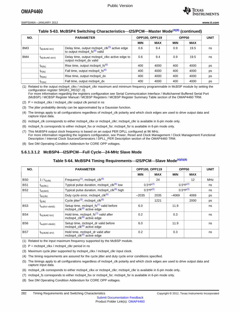
Public Version
OMAP4460
SWPS046A –JANUARY 2012 www.ti.com
Table 5-63. McBSP4 Switching Characteristics—I2S/PCM—Master Mode(4)(8) (continued)
NO. PARAMETER OPP100, OPP119 OPP50 UNIT
MIN MAX MIN MAX
BM3 td(clkAE-fsV) Delay time, output mcbsp4_clk(5) active edge 0.6 9.4 0.9 19.5 nsto output mcbsp4_fs(6) valid
BM4 td(clkxAE-dxV) Delay time, output mcbsp4_clkx active edge to 0.6 9.4 0.9 19.5 nsoutput mcbsp4_dx valid
tR(fs) Rise time, output mcbsp4_fs(6) 400 4000 400 4000 ps
tF(fs) Fall time, output mcbsp4_fs(6) 400 4000 400 4000 ps
tR(dx) Rise time, output mcbsp4_dx 400 4000 400 4000 ps
tF(dx) Fall time, output mcbsp4_dx 400 4000 400 4000 ps
(1) Related to the output mcbsp4_clkx / mcbsp4_clkr maximum and minimum frequency programmable in McBSP module by setting theconfiguration register SRGR1_REG[7..0].For more information regarding the registers configuration see Serial Communication Interface / Multichannel Buffered Serial Port(McBSP) / MCBSP Register Manual / MCBSP Registers / MCBSP Register Summary Table section of the OMAP4460 TRM.
(2) P = mcbsp4_clkx / mcbsp4_clkr output clk period in ns
(3) The jitter probability density can be approximated by a Gaussian function.
(4) The timings apply to all configurations regardless of mcbsp4_clk polarity and which clock edges are used to drive output data andcapture input data.
(5) mcbsp4_clk corresponds to either mcbsp4_clkx or mcbsp4_clkr; mcbsp4_clkr is available in 6-pin mode only.
(6) mcbsp4_fs corresponds to either mcbsp4_fsx or mcbsp4_fsr; mcbsp4_fsr is available in 6-pin mode only.
(7) This McBSP4 output clock frequency is based on an output PER DPLL configured at 96 MHz.For more information regarding the registers configuration, see Power, Reset and Clock Management / Clock Management FunctionalDescription / Internal Clock Sources/Generators / DPLL_PER Description section of the OMAP4460 TRM.
(8) See DM Operating Condition Addendum for CORE OPP voltages.
5.6.1.3.1.2 McBSP4—I2S/PCM—Full Cycle—24-MHz Slave Mode
Table 5-64. McBSP4 Timing Requirements—I2S/PCM—Slave Mode(4)(5)(8)
NO. PARAMETER OPP100, OPP119 OPP50 UNIT
MIN MAX MIN MAX
BS0 1 / tc(clk) Frequency(1), mcbsp4_clk(6) 24 12 MHz
BS1 tw(clkL) Typical pulse duration, mcbsp4_clk(6) low 0.5*P(2) 0.5*P(2) ns
BS2 tw(clkH) Typical pulse duration, mcbsp4_clk(6) high 0.5*P(2) 0.5*P(2) ns
tdc(clk) Duty cycle error, mcbsp4_clk(6) –2035 2035 –4069 4069 ps
tj(clk) Cycle jitter(3), mcbsp4_clk(6) 1221 2000 ps
BS3 tsu(fsV-clkAE) Setup time, mcbsp4_fs(7) valid before 6.0 11.9 nsmcbsp4_clk(6) active edge
BS4 th(clkAE-fsV) Hold time, mcbsp4_fs(7) valid after 0.2 0.3 nsmcbsp4_clk(6) active edge
BS6 tsu(drV-clkAE) Setup time, mcbsp4_dr valid before 6.0 11.9 nsmcbsp4_clk(6) active edge
BS7 th(clkAE-drV) Hold time, mcbsp4_dr valid after 0.2 0.3 nsmcbsp4_clk(6) active edge
(1) Related to the input maximum frequency supported by the McBSP module.
(2) P = mcbsp4_clkx / mcbsp4_clkr period in ns
(3) Maximum cycle jitter supported by mcbsp4_clkx / mcbsp4_clkr input clock.
(4) The timing requirements are assured for the cycle jitter and duty cycle error conditions specified.
(5) The timings apply to all configurations regardless of mcbsp4_clk polarity and which clock edges are used to drive output data andcapture input data.
(6) mcbsp4_clk corresponds to either mcbsp4_clkx or mcbsp4_clkr; mcbsp4_clkr is available in 6-pin mode only.
(7) mcbsp4_fs corresponds to either mcbsp4_fsx or mcbsp4_fsr; mcbsp4_fsr is available in 6-pin mode only.
(8) See DM Operating Condition Addendum for CORE OPP voltages.
282 Timing Requirements and Switching Characteristics Copyright © 2012, Texas Instruments Incorporated
Submit Documentation FeedbackProduct Folder Link(s): OMAP4460

Public Version
OMAP4460
www.ti.com SWPS046A –JANUARY 2012
Table 5-65. McBSP4 Switching Characteristics—I2S/PCM—Slave Mode(1)(2)
NO. PARAMETER OPP100, OPP119 OPP50 UNIT
MIN MAX MIN MAX
BS5 td(clkxAE-dxV) Delay time, input mcbsp4_clkx active edge to 0.9 23.2 1.0 40.0 nsoutput mcbsp4_dx valid
tR(dx) Rise time, output mcbsp4_dx 400 6500 400 6500 ps
tF(dx) Fall time, output mcbsp4_dx 400 6500 400 6500 ps
(1) The timings apply to all configurations regardless of mcbsp4_clk polarity and which clock edges are used to drive output data andcapture input data.
(2) See DM Operating Condition Addendum for CORE OPP voltages.
5.6.1.3.2 McBSP4—I2S/PCM—Half-Cycle—24-MHz Master and 12-MHz Slave
Table 5-67 through Table 5-70 assume testing over the recommended operating conditions and electricalcharacteristic conditions below.
Table 5-66. McBSP4 Timing Conditions—I2S/PCM(1)(2)(3)
SYSTEM CONDITION PARAMETER VALUE UNIT
MIN MAX
Input Conditions
tR Input signal rise time 400 6500 ps
tF Input signal fall time 400 6500 ps
PCB Conditions
Number of external peripherals 1
Far end load 5 pF
Trace length, point-to-point interconnect 9 cm
Characteristics impedance 30 55 Ω
(1) IO settings: MB[1:0] = 10 and LB0 = 0.For more information, see Control Module / Control Module Functional Description/ Functional Register Description / Signal IntegrityParameter Control Registers with Pad Group Assignment / I/Os with Combined Mode and Load Settings section of the OMAP4460TRM.
(2) In this table the rise and fall times are calculated for 10% to 90% of VDDS. For more information on the corresponding OMAP4 VDDSpower supply name, see Table 2-1, POWER [9] column with the ball name.
(3) To have an idea of the output OMAP4 ball load supported for this application, you can consider the following:Output OMAP4 ball load = Far End load + 1.34 pF/cm typical x trace length (cm).
5.6.1.3.2.1 McBSP4—I2S/PCM—Half-Cycle—24-MHz Master Mode
Table 5-67. McBSP4 Timing Requirements—I2S/PCM—Master Mode(1)(3)
NO. PARAMETER OPP100, OPP119 OPP50 UNIT
MIN MAX MIN MAX
BM5 tsu(drV-clkAE) Setup time, mcbsp4_dr valid before 5.3 11.6 nsmcbsp4_clk(2) active edge
BM6 th(clkAE-drV) Hold time, mcbsp4_dr valid after 5.3 11.3 nsmcbsp4_clk(2) active edge
(1) The timings apply to all configurations regardless of mcbsp4_clk polarity and which clock edges are used to drive output data andcapture input data.
(2) mcbsp4_clk corresponds to either mcbsp4_clkx or mcbsp4_clkr; mcbsp4_clkr is available in 6-pin mode only.
(3) See DM Operating Condition Addendum for CORE OPP voltages.
Copyright © 2012, Texas Instruments Incorporated Timing Requirements and Switching Characteristics 283Submit Documentation Feedback
Product Folder Link(s): OMAP4460

Public Version
OMAP4460
SWPS046A –JANUARY 2012 www.ti.com
Table 5-68. McBSP4 Switching Characteristics—I2S/PCM—Master Mode(4)(8)
NO. PARAMETER OPP100, OPP119 OPP50 UNIT
MIN MAX MIN MAX
BM0 1 / tc(clk) Frequency(1), output mcbsp4_clk clock 24(7) 12(7) MHz
BM1 tw(clkL) Typical pulse duration, output mcbsp4_clk low 0.5*P(2) 0.5*P(2) ns
BM2 tw(clkH) Typical pulse duration, output mcbsp4_clk 0.5*P(2) 0.5*P(2) nshigh
tdc(clk) Duty cycle error, output mcbsp4_clk –2035 2035 –4069 4069 ps
tj(clk) Jitter standard deviation(3), output mcbsp4_clk 65 65 ps
tR(clk) Rise time, output mcbsp4_clk 400 6500 400 6500 ps
tF(clk) Fall time, output mcbsp4_clk 400 6500 400 6500 ps
BM3 td(clkAE-fsV) Delay time, output mcbsp4_clk active edge to –7.1 11.7 –15.2 23.6 nsoutput mcbsp4_fs(6) valid
BM4 td(clkxAE-dxV) Delay time, output mcbsp4_clkx active edge to –7.1 11.7 –15.2 23.6 nsoutput mcbsp4_dx valid
tR(fs) Rise time, output mcbsp4_fs(6) 400 6500 400 6500 ps
tF(fs) Fall time, output mcbsp4_fs(6) 400 6500 400 6500 ps
tR(dx) Rise time, output mcbsp4_dx 400 6500 400 6500 ps
tF(dx) Fall time, output mcbsp4_dx 400 6500 400 6500 ps
(1) Related to the output mcbsp4_clkx / mcbsp4_clkr maximum and minimum frequency programmable in McBSP module by setting theconfiguration register SRGR1_REG[7..0].For more information regarding the registers configuration see the Serial Communication Interface / Multichannel Buffered Serial Port(McBSP) / MCBSP Register Manual / MCBSP Registers / MCBSP Register Summary Table section of the OMAP4460 TRM.
(2) P = mcbsp4_clkx / mcbsp4_clkr output clk period in ns.
(3) The jitter probability density can be approximated by a Gaussian function.
(4) The timings apply to all configurations regardless of mcbsp4_clk polarity and which clock edges are used to drive output data andcapture input data.
(5) mcbsp4_clk corresponds to either mcbsp4_clkx or mcbsp4_clkr; mcbsp4_clkr is available in 6-pin mode only.
(6) mcbsp4_fs corresponds to either mcbsp4_fsx or mcbsp4_fsr; mcbsp4_fsr is available in 6-pin mode only.
(7) This McBSP4 output clock frequency is based on an output PER DPLL configured at 96 MHz.For more information regarding the registers configuration, see the Power, Reset and Clock Management / Clock ManagementFunctional Description / Internal Clock Sources/Generators / DPLL_PER Description section of the OMAP4460 TRM.
(8) See DM Operating Condition Addendum for CORE OPP voltages.
5.6.1.3.2.2 McBSP4—I2S/PCM—Half-Cycle—12-MHz Slave Mode
Table 5-69. McBSP4 Timing Requirements—I2S/PCM—Slave Mode(4)(5)(8)
NO. PARAMETER OPP100, OPP119 OPP50 UNIT
MIN MAX MIN MAX
BS0 1 / tc(clk) Frequency(1), mcbsp4_clk(6) 12 6 MHz
BS1 tw(clkL) Typical pulse duration, mcbsp4_clk(6) low 0.5*P(2) 0.5*P(2) ns
BS2 tw(clkH) Typical pulse duration, mcbsp4_clk(6) high 0.5*P(2) 0.5*P(2) ns
tdc(clk) Duty cycle error, mcbsp4_clk(6) –4069 4069 –8138 8138 ps
tj(clk) Cycle jitter(3), mcbsp4_clk(6) 2000 2000 ps
BS3 tsu(fsV-clkAE) Setup time, mcbsp4_fs(7) valid before 13.2 26.7 nsmcbsp4_clk(6) active edge
BS4 th(clkAE-fsV) Hold time, mcbsp4_fs(7) valid after 0.3 0.3 nsmcbsp4_clk(6) active edge
BS6 tsu(drV-clkAE) Setup time, mcbsp4_dr valid before 13.2 26.7 nsmcbsp4_clk(6) active edge
BS7 th(clkAE-drV) Hold time, mcbsp4_dr valid after 0.3 0.3 nsmcbsp4_clk(6) active edge
284 Timing Requirements and Switching Characteristics Copyright © 2012, Texas Instruments Incorporated
Submit Documentation FeedbackProduct Folder Link(s): OMAP4460

mcbsp4_clk
mcbsp4_fs
mcbsp4_dx
mcbsp4_dr
DX7 DX6 DX0
DR7 DR6 DR0
BM3 BM3
BM4
BM0 BM1 BM2
BM5
BM6
SWPS040-119
BM4 BM4
Public Version
OMAP4460
www.ti.com SWPS046A –JANUARY 2012
(1) Related to the input maximum frequency supported by the McBSP module.
(2) P = mcbsp4_clkx / mcbsp4_clkr period in ns
(3) Maximum cycle jitter supported by mcbsp4_clkx / mcbsp4_clkr input clock.
(4) The timing requirements are assured for the cycle jitter and duty cycle error conditions specified.
(5) The timings apply to all configurations regardless of mcbsp4_clk polarity and which clock edges are used to drive output data andcapture input data.
(6) mcbsp4_clk corresponds to either mcbsp4_clkx or mcbsp4_clkr; mcbsp4_clkr is available in 6-pin mode only.
(7) mcbsp4_fs corresponds to either mcbsp4_fsx or mcbsp4_fsr; mcbsp4_fsr is available in 6-pin mode only.
(8) See DM Operating Condition Addendum for CORE OPP voltages.
Table 5-70. McBSP4 Switching Characteristics—I2S/PCM—Slave Mode(1)(2)
NO. PARAMETER OPP100, OPP119 OPP50 UNIT
MIN MAX MIN MAX
BS5 td(clkxAE-dxV) Delay time, input mcbsp4_clkx active edge to 1.0 23.2 1.1 40.0 nsoutput mcbsp4_dx valid
tR(dx) Rise time, output mcbsp4_dx 400 6500 400 6500 ps
tF(dx) Fall time, output mcbsp4_dx 400 6500 400 6500 ps
(1) The timings apply to all configurations regardless of mcbsp4_clk polarity and which clock edges are used to drive output data andcapture input data.
(2) See DM Operating Condition Addendum for CORE OPP voltages.
Figure 5-65. McBSP4—I2S/PCM—Master Mode(1)(2)(3)(4)(5)
(1) mcbsp4_clk corresponds to either mcbsp4_clkx or mcbsp4_clkr; mcbsp4_fs corresponds to either mcbsp4_fsx or mcbsp4_fsr.McBSP in 6-pin mode: dx and dr as data pins; clkx, clkr, fsx, and fsr as control pins.McBSP in 4-pin mode: dx and dr as data pins; clkx and fsx pins as control pins. The clkx and fsx pins are internally looped back, viasoftware configuration, respectively to the clkr and fsr internal signals for data receive.
(2) The polarity of McBSP frame synchronization is software configurable.
(3) The active clock edge selection of mcbsp4_clk (rising or falling) on which mcbsp4_dx data is latched and mcbsp4_dr data is sampled issoftware configurable.
(4) Timing diagrams are for data delay set to 1.
(5) For more information regarding the registers configuration see the Serial Communication Interface / Multichannel Buffered Serial Port(McBSP) MCBSP Register Manual / MCBSP Registers / MCBSP Register Summary Table section of the OMAP4460 TRM.
Copyright © 2012, Texas Instruments Incorporated Timing Requirements and Switching Characteristics 285Submit Documentation Feedback
Product Folder Link(s): OMAP4460

mcbsp4_clk
mcbsp4_fs
mcbsp4_dx
mcbsp4_dr
DX7 DX6 DX0
DR7 DR6 DR0
BS4
BS5
BS0 BS1 BS2
BS6
BS7
BS5 BS5
BS3
SWPS040-120
Public Version
OMAP4460
SWPS046A –JANUARY 2012 www.ti.com
Figure 5-66. McBSP4—I2S/PCM—Slave Mode(1)(2)(3)(4)(5)
(1) mcbsp4_clk corresponds to either mcbsp4_clkx or mcbsp4_clkr; mcbsp4_fs corresponds to either mcbsp4_fsx or mcbsp4_fsr.McBSP in 6-pin mode: dx and dr as data pins; clkx, clkr, fsx, and fsr as control pins.McBSP in 4-pin mode: dx and dr as data pins; clkx and fsx pins as control pins. The clkx and fsx pins are internally looped back, viasoftware configuration, respectively to the clkr and fsr internal signals for data receive.
(2) The polarity of McBSP frame synchronization is software configurable.
(3) The active clock edge selection of mcbsp4_clk (rising or falling) on which mcbsp4_dx data is latched and mcbsp4_dr data is sampled issoftware configurable.
(4) Timing diagrams are for data delay set to 1.
(5) For more information regarding the registers configuration see Serial Communication Interface / Multichannel Buffered Serial Port(McBSP) MCBSP Register Manual / MCBSP Registers / MCBSP Register Summary Table section of the OMAP4460 TRM.
5.6.2 Multichannel Buffered Serial Port (McASP)
NOTEFor more information, see the Serial Communication Interface section of the OMAP4460TRM.
Table 5-72 assumes testing over the recommended operating conditions and electrical characteristicconditions below (see Figure 5-67).
Table 5-71. McASP Timing Conditions(1)(2)(3)
SYSTEM CONDITION PARAMETER VALUE UNIT
MIN MAX
PCB Conditions
Number of external peripherals 1
Far end load 7 pF
Trace length, point-to-point interconnect 10 cm
Characteristics impedance 30 60 Ω
(1) O settings: MB[1:0] = 10 and LB0 = 0.For more information, see Control Module / Control Module Functional Description/ Functional Register Description / Signal IntegrityParameter Control Registers with Pad Group Assignment / 50-Ω Output Buffer I/Os with Combined Mode and Load Settings section ofthe OMAP4460 TRM.
(2) In this table the rise and fall times are calculated for 10% to 90% of VDDS. For more information on the corresponding OMAP4 VDDSpower supply name, see Table 2-1, POWER [9] column with the ball name.
(3) To have an idea of the output OMAP4 ball load supported for this application, you can consider the following:Output OMAP4 ball load = Far End load + 1.34 pF/cm typical x trace length (cm).
286 Timing Requirements and Switching Characteristics Copyright © 2012, Texas Instruments Incorporated
Submit Documentation FeedbackProduct Folder Link(s): OMAP4460
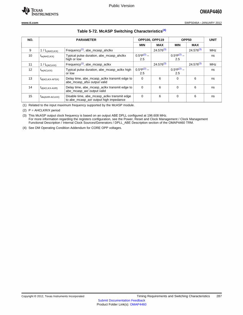
Public Version
OMAP4460
www.ti.com SWPS046A –JANUARY 2012
Table 5-72. McASP Switching Characteristics(4)
NO. PARAMETER OPP100, OPP119 OPP50 UNIT
MIN MAX MIN MAX
9 1 / tc(AHCLKX) Frequency(1), abe_mcasp_ahclkx 24.576(3) 24.576(3) MHz
10 tw(AHCLKX) Typical pulse duration, abe_mcasp_ahclkx 0.5*P(2) – 0.5*P(2) – nshigh or low 2.5 2.5
11 1 / tc(ACLKX) Frequency(1), abe_mcasp_aclkx 24.576(3) 24.576(3) MHz
12 tw(ACLKX) Typical pulse duration, abe_mcasp_aclkx high 0.5*P(2) – 0.5*P(2) – nsor low 2.5 2.5
13 td(ACLKX-AFSX) Delay time, abe_mcasp_aclkx transmit edge to 0 6 0 6 nsabe_mcasp_afsx output valid
14 td(ACLKX-AXR) Delay time, abe_mcasp_aclkx transmit edge to 0 6 0 6 nsabe_mcasp_axr output valid
15 tdis(AXR-ACLKX) Disable time, abe_mcasp_aclkx transmit edge 0 6 0 6 nsto abe_mcasp_axr output high impedance
(1) Related to the input maximum frequency supported by the McASP module.
(2) P = AHCLKR/X period
(3) This McASP output clock frequency is based on an output ABE DPLL configured at 196.608 MHz.For more information regarding the registers configuration, see the Power, Reset and Clock Management / Clock ManagementFunctional Description / Internal Clock Sources/Generators / DPLL_ABE Description section of the OMAP4460 TRM.
(4) See DM Operating Condition Addendum for CORE OPP voltages.
Copyright © 2012, Texas Instruments Incorporated Timing Requirements and Switching Characteristics 287Submit Documentation Feedback
Product Folder Link(s): OMAP4460

MCA[x]_ACLKR/X (CLKRP = CLKXP = 1)(1)
MCA[x]_ACLKR/X (CLKRP = CLKXP = 0)(2)
MCA[x]_ACLKR/X (Falling Edge Polarity)
MCA[x]_AHCLKR/X (Rising Edge Polarity)
SWPS040-105
A0 A1 A30 A31 B0 B1 B30 B31 C0 C1 C2 C3 C31
MCA[x]_AFSR/X (Bit Width, 0 Bit Delay)
MCA[x]_AFSR/X (Bit Width, 1 Bit Delay)
MCA[x]_AFSR/X (Bit Width, 2 Bit Delay)
MCA[x]_AFSR/X (Slot Width, 0 Bit Delay)
MCA[x]_AFSR/X (Slot Width, 1 Bit Delay)
MCA[x]_AFSR/X (Slot Width, 2 Bit Delay)
MCA[x]_AXR[x] (Data Out/Transmit)
9
10
10
1313
1313
13 1313
1112
12
14
15
Public Version
OMAP4460
SWPS046A –JANUARY 2012 www.ti.com
Figure 5-67. McASP Output Timing(1)(2)
(1) For CLKRP = CLKXP = 1, the McASP transmitter is configured for falling edge (to shift data out) and the McASP receiver is configuredfor rising edge (to shift data in).
(2) For CLKRP = CLKXP = 0, the McASP transmitter is configured for rising edge (to shift data out) and the McASP receiver is configuredfor falling edge (to shift data in).
5.6.3 Multichannel Serial Port Interface (McSPI)
NOTEFor more information, see the Serial Communication Interface section of the OMAP4460TRM.
McSPI allows a duplex, synchronous, serial communication between a local host and SPI compliantexternal devices. The following timings are applicable to the different configurations of McSPI inmaster/slave mode for any McSPI and any channel (n).
288 Timing Requirements and Switching Characteristics Copyright © 2012, Texas Instruments Incorporated
Submit Documentation FeedbackProduct Folder Link(s): OMAP4460
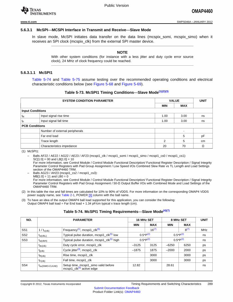
Public Version
OMAP4460
www.ti.com SWPS046A –JANUARY 2012
5.6.3.1 McSPI—MCSPI Interface in Transmit and Receive—Slave Mode
In slave mode, McSPI initiates data transfer on the data lines (mcspix_somi, mcspix_simo) when itreceives an SPI clock (mcspix_clk) from the external SPI master device.
NOTEWith other system conditions (for instance with a less jitter and duty cycle error sourceclock), 24 MHz of clock frequency could be reached.
5.6.3.1.1 McSPI1
Table 5-74 and Table 5-75 assume testing over the recommended operating conditions and electricalcharacteristic conditions below (see Figure 5-68 and Figure 5-69).
Table 5-73. McSPI1 Timing Conditions—Slave Mode(1)(2)(3)
SYSTEM CONDITION PARAMETER VALUE UNIT
MIN MAX
Input Conditions
tR Input signal rise time 1.00 3.00 ns
tF Input signal fall time 1.00 3.00 ns
PCB Conditions
Number of external peripherals -
Far end load 5 pF
Trace length 2 5 cm
Characteristics impedance 20 70 Ω
(1) McSPI1:
– Balls AF22 / AE22 / AG22 / AE23 / AF23 (mcspi1_clk / mcspi1_somi / mcspi1_simo / mcspi1_cs0 / mcspi1_cs1):SC[1:0] = 00 and LB[1:0] = 10For more information, see Control Module / Control Module Functional Description/ Functional Register Description / Signal IntegrityParameter Control Registers with Pad Group Assignment / Low Speed I/Os Combined Slew Rate vs TL Length and Load Settingssection of the OMAP4460 TRM.
– Balls AG23 / AH23 (mcspi1_cs2 / mcspi1_cs3):MB[1:0] = 11 and LB0 = 0For more information, see Control Module / Control Module Functional Description/ Functional Register Description / Signal IntegrityParameter Control Registers with Pad Group Assignment / 50-Ω Output Buffer I/Os with Combined Mode and Load Settings of theOMAP4460 TRM.
(2) In this table the rise and fall times are calculated for 10% to 90% of VDDS. For more information on the corresponding OMAP4 VDDSpower supply name, see Table 2-1, POWER [9] column with the ball name.
(3) To have an idea of the output OMAP4 ball load supported for this application, you can consider the following:Output OMAP4 ball load = Far End load + 1.34 pF/cm typical x trace length (cm).
Table 5-74. McSPI1 Timing Requirements—Slave Mode(4)(7)
NO. PARAMETER 16 MHz SET 8 MHz SET UNIT
MIN MAX MIN MAX
SS1 1 / tc(clk) Frequency(1), mcspi1_clk(5) 16(7) 8(7) MHz
SS2 tw(clkL) Typical pulse duration, mcspi1_clk(5) low 0.5*P(2) 0.5*P(2) ns
SS3 tw(clkH) Typical pulse duration, mcspi1_clk(5) high 0.5*P(2) 0.5*P(2) ns
tdc(clk) Duty cycle error, mcspi1_clk –3125 3125 –6250 6250 ps
tj(clk) Cycle jitter(3), mcspi1_clk –1875 1875 –2000 2000 ps
tR(clk) Rise time, mcspi1_clk 3000 3000 ps
tF(clk) Fall time, mcspi1_clk 3000 3000 ps
SS4 tsu(SIMO-CLKAE) Setup time, mcspi1_simo valid before 12.82 28.61 nsmcspi1_clk(5) active edge
Copyright © 2012, Texas Instruments Incorporated Timing Requirements and Switching Characteristics 289Submit Documentation Feedback
Product Folder Link(s): OMAP4460

Public Version
OMAP4460
SWPS046A –JANUARY 2012 www.ti.com
Table 5-74. McSPI1 Timing Requirements—Slave Mode(4)(7) (continued)
NO. PARAMETER 16 MHz SET 8 MHz SET UNIT
MIN MAX MIN MAX
SS5 th(clkAE-SIMO) Hold time, mcspi1_simo valid after 12.82 28.61 nsmcspi1_clk(5) active edge
SS8 tsu(CS-CLKAE) Setup time, mcspi1_cs0 valid before 12.82 28.61 nsmcspi1_clk(5) first edge
SS9 th(clkAE-CS) Hold time, mcspi1_cs0 valid after 12.82 28.61 nsmcspi1_clk(5) last edge
(1) Related to the input maximum frequency supported by the McSPI module.
(2) P = mcspi1_clk period in ns
(3) Maximum cycle jitter supported by mcspi1_clk input clock.
(4) The timing requirements are assured for the cycle jitter and duty cycle error conditions specified.
(5) This timing applies to all configurations regardless of mcspi1_clk polarity and which clock edges are used to drive output data andcapture input data.
(6) With other system conditions (for instance with a less jitter and duty cycle error source clock), 24 MHz of clock frequency could bereached.
(7) The timings requirements described are applicable to both CORE OPP50 and OPP100 operating points.
Table 5-75. McSPI1 Switching Characteristics—Slave Mode(2)(3)
NO. PARAMETER 16 MHz SET(3) 8 MHz SET(3) UNIT
MIN MAX MIN MAX
SS6 td(clk-SOMI) Delay time, mcspi1_clk(1) active edge to –4.66 18.41 –12.01 37.32 nsmcspi1_somi transition
SS7 td(CS-SOMI) Delay time, mcspi1_cs0 active edge PHA = 0(2) 18.41 37.32 nsto mcspi1_somi transition
tR(SOMI) Rise time, mcspi1_somi 4000.0 4000.0 ps
tF(SOMI) Fall time, mcspi1_somi 4000.0 4000.0 ps
(1) The polarity of mcspi1_clk and the active edge (rising or falling) on which mcspi1_simo is driven and mcspi1_somi is latched is allsoftware configurable:
– mcspi1_clk phase programmable with the bit PHA of MCSPI_Ch(i)CONF register: PHA = 0 (Modes 0 and 2).
For more information, see the McSPI environment chapter, Data Format Configurations section of the OMAP4460 TRM for modes andphase correspondence description.
(2) This timing applies to all configurations regardless of mcspi1_clk polarity and which clock edges are used to drive output data andcapture input data.
(3) The timings requirements described are applicable to both CORE OPP50 and OPP100 operating points.
5.6.3.1.2 McSPI2 and McSPI4
Table 5-77 and Table 5-78 assume testing over the recommended operating conditions and electricalcharacteristic conditions below (see Figure 5-68 and Figure 5-69).
Table 5-76. McSPI2 and McSPI4 Timing Conditions—Slave Mode(1)(2)(3)
SYSTEM CONDITION PARAMETER VALUE UNIT
MIN MAX
Input Conditions
tR Input signal rise time 1.00 4.00 ns
tF Input signal fall time 1.00 4.00 ns
PCB Conditions
Number of external peripherals -
Far end load 5 pF
Trace length 2 5 cm
Characteristics impedance 20 60 Ω
290 Timing Requirements and Switching Characteristics Copyright © 2012, Texas Instruments Incorporated
Submit Documentation FeedbackProduct Folder Link(s): OMAP4460
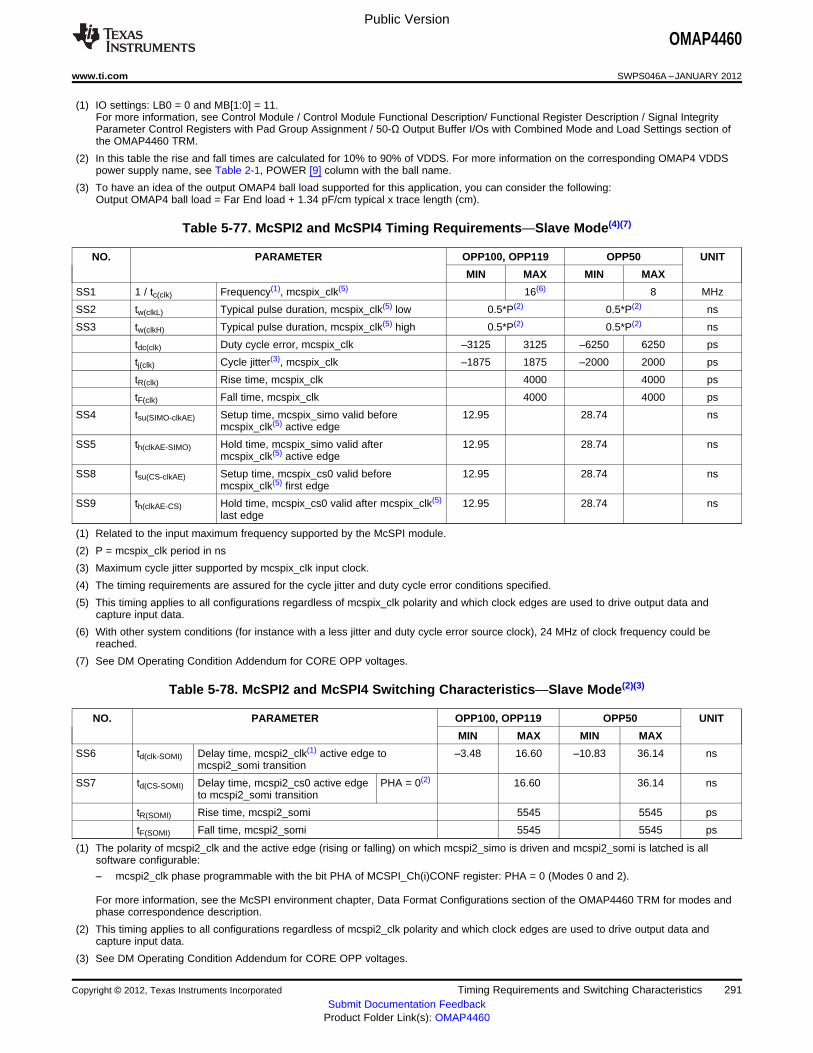
Public Version
OMAP4460
www.ti.com SWPS046A –JANUARY 2012
(1) IO settings: LB0 = 0 and MB[1:0] = 11.For more information, see Control Module / Control Module Functional Description/ Functional Register Description / Signal IntegrityParameter Control Registers with Pad Group Assignment / 50-Ω Output Buffer I/Os with Combined Mode and Load Settings section ofthe OMAP4460 TRM.
(2) In this table the rise and fall times are calculated for 10% to 90% of VDDS. For more information on the corresponding OMAP4 VDDSpower supply name, see Table 2-1, POWER [9] column with the ball name.
(3) To have an idea of the output OMAP4 ball load supported for this application, you can consider the following:Output OMAP4 ball load = Far End load + 1.34 pF/cm typical x trace length (cm).
Table 5-77. McSPI2 and McSPI4 Timing Requirements—Slave Mode(4)(7)
NO. PARAMETER OPP100, OPP119 OPP50 UNIT
MIN MAX MIN MAX
SS1 1 / tc(clk) Frequency(1), mcspix_clk(5) 16(6) 8 MHz
SS2 tw(clkL) Typical pulse duration, mcspix_clk(5) low 0.5*P(2) 0.5*P(2) ns
SS3 tw(clkH) Typical pulse duration, mcspix_clk(5) high 0.5*P(2) 0.5*P(2) ns
tdc(clk) Duty cycle error, mcspix_clk –3125 3125 –6250 6250 ps
tj(clk) Cycle jitter(3), mcspix_clk –1875 1875 –2000 2000 ps
tR(clk) Rise time, mcspix_clk 4000 4000 ps
tF(clk) Fall time, mcspix_clk 4000 4000 ps
SS4 tsu(SIMO-clkAE) Setup time, mcspix_simo valid before 12.95 28.74 nsmcspix_clk(5) active edge
SS5 th(clkAE-SIMO) Hold time, mcspix_simo valid after 12.95 28.74 nsmcspix_clk(5) active edge
SS8 tsu(CS-clkAE) Setup time, mcspix_cs0 valid before 12.95 28.74 nsmcspix_clk(5) first edge
SS9 th(clkAE-CS) Hold time, mcspix_cs0 valid after mcspix_clk(5) 12.95 28.74 nslast edge
(1) Related to the input maximum frequency supported by the McSPI module.
(2) P = mcspix_clk period in ns
(3) Maximum cycle jitter supported by mcspix_clk input clock.
(4) The timing requirements are assured for the cycle jitter and duty cycle error conditions specified.
(5) This timing applies to all configurations regardless of mcspix_clk polarity and which clock edges are used to drive output data andcapture input data.
(6) With other system conditions (for instance with a less jitter and duty cycle error source clock), 24 MHz of clock frequency could bereached.
(7) See DM Operating Condition Addendum for CORE OPP voltages.
Table 5-78. McSPI2 and McSPI4 Switching Characteristics—Slave Mode(2)(3)
NO. PARAMETER OPP100, OPP119 OPP50 UNIT
MIN MAX MIN MAX
SS6 td(clk-SOMI) Delay time, mcspi2_clk(1) active edge to –3.48 16.60 –10.83 36.14 nsmcspi2_somi transition
SS7 td(CS-SOMI) Delay time, mcspi2_cs0 active edge PHA = 0(2) 16.60 36.14 nsto mcspi2_somi transition
tR(SOMI) Rise time, mcspi2_somi 5545 5545 ps
tF(SOMI) Fall time, mcspi2_somi 5545 5545 ps
(1) The polarity of mcspi2_clk and the active edge (rising or falling) on which mcspi2_simo is driven and mcspi2_somi is latched is allsoftware configurable:
– mcspi2_clk phase programmable with the bit PHA of MCSPI_Ch(i)CONF register: PHA = 0 (Modes 0 and 2).
For more information, see the McSPI environment chapter, Data Format Configurations section of the OMAP4460 TRM for modes andphase correspondence description.
(2) This timing applies to all configurations regardless of mcspi2_clk polarity and which clock edges are used to drive output data andcapture input data.
(3) See DM Operating Condition Addendum for CORE OPP voltages.
Copyright © 2012, Texas Instruments Incorporated Timing Requirements and Switching Characteristics 291Submit Documentation Feedback
Product Folder Link(s): OMAP4460

Public Version
OMAP4460
SWPS046A –JANUARY 2012 www.ti.com
5.6.3.1.3 McSPI3
Table 5-80 and Table 5-81 assume testing over the recommended operating conditions and electricalcharacteristic conditions below (see Figure 5-68 and Figure 5-69).
Table 5-79. McSPI3 Timing Conditions—Slave Mode(1)(2)(3)
SYSTEM CONDITION PARAMETER VALUE UNIT
MIN MAX
Input Conditions
tR Input signal rise time 1.00 4.00 ns
tF Input signal fall time 1.00 4.00 ns
PCB Conditions
Number of external peripherals -
Far end load 5 pF
Trace length 2 5 cm
Characteristics impedance 20 50 Ω
(1) IO settings: DS0 = 0.For more information, see Control Module / Control Module Functional Description/ Functional Register Description / Signal IntegrityParameter Control Registers with Pad Group Assignment / I/O cells with Configurable Output Driver Impedance of the OMAP4460 TRM.
(2) In this table the rise and fall times are calculated for 10% to 90% of VDDS. For more information on the corresponding OMAP4 VDDSpower supply name, see Table 2-1, POWER [9] column with the ball name.
(3) To have an idea of the output OMAP4 ball load supported for this application, you can consider the following:Output OMAP4 ball load = Far End load + 1.34 pF/cm typical x trace length (cm).
Table 5-80. McSPI3 Timing Requirements—Slave Mode(4)(7)
NO. PARAMETER OPP100, OPP119 OPP50 UNIT
MIN MAX MIN MAX
SS1 1 / tc(clk) Frequency(1), mcspi3_clk(5) 16(6) 8 MHz
SS2 tw(clkL) Typical pulse duration, mcspi3_clk(5) low 0.5*P(2) 0.5*P(2) ns
SS3 tw(clkH) Typical pulse duration, mcspi3_clk(5) high 0.5*P(2) 0.5*P(2) ns
tdc(clk) Duty cycle error, mcspi3_clk –3125 3125 –6250 6250 ps
tj(clk) Cycle jitter(3), mcspi3_clk –1875 1875 –2000 2000 ps
tR(clk) Rise time, mcspi3_clk 4000 4000 ps
tF(clk) Fall time, mcspi3_clk 4000 4000 ps
SS4 tsu(SIMO-CLKAE) Setup time, mcspi3_simo valid before 12.92 28.70 nsmcspi3_clk(5) active edge
SS5 th(clkAE-SIMO) Hold time, mcspi3_simo valid after 12.92 28.70 nsmcspi3_clk(5) active edge
SS8 tsu(CS-CLKAE) Setup time, mcspi3_cs0 valid before 12.92 28.70 nsmcspi3_clk(5) first edge
SS9 th(clkAE-CS) Hold time, mcspi3_cs0 valid after 12.92 28.70 nsmcspi3_clk(5) last edge
(1) Related to the input maximum frequency supported by the McSPI module.
(2) P = mcspi3_clk period in ns
(3) Maximum cycle jitter supported by mcspi3_clk input clock.
(4) The timing requirements are assured for the cycle jitter and duty cycle error conditions specified.
(5) This timing applies to all configurations regardless of mcspi3_clk polarity and which clock edges are used to drive output data andcapture input data.
(6) With other system conditions (for instance with a less jitter and duty cycle error source clock), 24 MHz of clock frequency could bereached.
(7) See DM Operating Condition Addendum for CORE OPP voltages.
292 Timing Requirements and Switching Characteristics Copyright © 2012, Texas Instruments Incorporated
Submit Documentation FeedbackProduct Folder Link(s): OMAP4460

mcspi_cs(IN)
mcspi_clk(IN)
mcspi_clk(IN)
mcspi_somi(OUT)
mcspi_cs(IN)
mcspi_clk(IN)
mcspi_clk(IN)
mcspi_somi(OUT)
Bit n-1 Bit n-2 Bit n-3 Bit n-4 Bit 0
Bit n-1 Bit n-2 Bit n-3 Bit 1 Bit 0
PHA=0
EPOL=1
POL=0
POL=1
POL=0
POL=1
PHA=1
EPOL=1
SS6
SS3
SS1
SS3
SS1
SS3
SS1
SS2
SS1
SS6
SS6
SS8 SS9
SS7
SS8
SS2
SS3
SS2
SS2
SS6 SS6SS6
SS9
SWPS040-054
Public Version
OMAP4460
www.ti.com SWPS046A –JANUARY 2012
Table 5-81. McSPI3 Switching Characteristics—Slave Mode(2)(3)
NO. PARAMETER OPP100, OPP119 OPP50 UNIT
MIN MAX MIN MAX
SS6 td(clk-SOMI) Delay time, mcspi3_clk(1) active edge to –3.99 17.12 –11.34 36.66 nsmcspi3_somi transition
SS7 td(CS-SOMI) Delay time, mcspi3_cs0 active edge PHA = 0 17.12 36.66 nsto mcspi3_somi transition
tR(SOMI) Rise time, mcspi3_somi 5001 5001 ps
tF(SOMI) Fall time, mcspi3_somi 5001 5001 ps
(1) The polarity of mcspi3_clk and the active edge (rising or falling) on which mcspi3_simo is driven and mcspi3_somi is latched is allsoftware configurable:
– mcspi3_clk phase programmable with the bit PHA of MCSPI_Ch(i)CONF register: PHA = 0 (Modes 0 and 2).
For more information, see the McSPI environment chapter, Data Format Configurations section of the OMAP4460 TRM for modes andphase correspondence description.
(2) This timing applies to all configurations regardless of mcspi3_clk polarity and which clock edges are used to drive output data andcapture input data.
(3) See DM Operating Condition Addendum for CORE OPP voltages.
Figure 5-68. McSPI—Slave Mode—Transmit(1)(2)(3)
Copyright © 2012, Texas Instruments Incorporated Timing Requirements and Switching Characteristics 293Submit Documentation Feedback
Product Folder Link(s): OMAP4460

mcspi_cs(IN)
mcspi_clk(IN)
mcspi_clk(IN)
mcspi_simo(IN)
mcspi_cs(IN)
mcspi_clk(IN)
mcspi_clk(IN)
mcspi_simo(IN)
Bit n-1 Bit n-2 Bit n-3 Bit n-4 Bit 0
Bit n-1 Bit n-2 Bit n-3 Bit 1 Bit0
PHA=0
EPOL=1
POL=0
POL=1
POL=0
POL=1
PHA=1
EPOL=1
SS3
SS1
SS3
SS1
SS3
SS1
SS2
SS1
SS8 SS9
SS8 SS9
SS2
SS3
SS2
SS2
SS4
SS5
SS5
SS4
SS4
SS5
SS4
SS5
SWPS040-055
Public Version
OMAP4460
SWPS046A –JANUARY 2012 www.ti.com
(1) The active clock edge selection of mcspix_clk (rising or falling) on which mcspix_simo is driven and mcspix_somi data is latched issoftware configurable with the bit MCSPI_Ch(i)CONF[1] = POL and the bit MCSPI_Ch(i)CONF[0] = PHA.
(2) The polarity of mcspix_cs is software configurable with the bit MCSPI_Ch(i)CONF[6] = EPOL.
(3) In mcspix, x is equal to 1, 2, 3, or 4.
Figure 5-69. McSPI—Slave Mode—Receive(1)(2)(3)
(1) The active clock edge selection of mcspix_clk (rising or falling) on which mcspix_simo is driven and mcspix_somi data is latched issoftware configurable with the bit MCSPI_Ch(i)CONF[1] = POL and the bit MCSPI_Ch(i)CONF[0] = PHA.
(2) The polarity of mcspix_cs is software configurable with the bit MCSPI_Ch(i)CONF[6] = EPOL.
(3) In mcspix, x is equal to 1, 2, 3, or 4.
5.6.3.2 McSPI—McSPI Interface in Transmit and Receive—Master Mode
In master mode, McSPI supports multichannel communication. McSPI initiates a data transfer on the datalines (SPIDAT [1:0]) and generates clock (SPICLK) and control signals (SPIEN) to a single SPI slavedevice at a time.
294 Timing Requirements and Switching Characteristics Copyright © 2012, Texas Instruments Incorporated
Submit Documentation FeedbackProduct Folder Link(s): OMAP4460
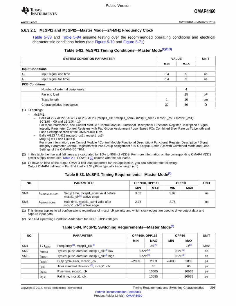
Public Version
OMAP4460
www.ti.com SWPS046A –JANUARY 2012
5.6.3.2.1 McSPI1 and McSPI2—Master Mode—24-MHz Frequency Clock
Table 5-83 and Table 5-84 assume testing over the recommended operating conditions and electricalcharacteristic conditions below (see Figure 5-70 and Figure 5-71).
Table 5-82. McSPI1 Timing Conditions—Master Mode(1)(2)(3)
SYSTEM CONDITION PARAMETER VALUE UNIT
MIN MAX
Input Conditions
tR Input signal rise time 0.4 5 ns
tF Input signal fall time 0.4 5 ns
PCB Conditions
Number of external peripherals 4
Far end load 25 pF
Trace length 1 10 cm
Characteristics impedance 30 60 Ω
(1) IO settings:
– McSPI1:– Balls AF22 / AE22 / AG22 / AE23 / AF23 (mcspi1_clk / mcspi1_somi / mcspi1_simo / mcspi1_cs0 / mcspi1_cs1):
SC[1:0] = 00 and LB[1:0] = 10For more information, see Control Module / Control Module Functional Description/ Functional Register Description / SignalIntegrity Parameter Control Registers with Pad Group Assignment / Low Speed I/Os Combined Slew Rate vs TL Length andLoad Settings section of the OMAP4460 TRM.
– Balls AG23 / AH23 (mcspi1_cs2 / mcspi1_cs3):MB[1:0] = 11 and LB0 = 0For more information, see Control Module / Control Module Functional Description/ Functional Register Description / SignalIntegrity Parameter Control Registers with Pad Group Assignment / 50-Ω Output Buffer I/Os with Combined Mode and LoadSettings of the OMAP4460 TRM.
(2) In this table the rise and fall times are calculated for 10% to 90% of VDDS. For more information on the corresponding OMAP4 VDDSpower supply name, see Table 2-1, POWER [9] column with the ball name.
(3) To have an idea of the output OMAP4 ball load supported for this application, you can consider the following:Output OMAP4 ball load = Far End load + 1.34 pF/cm typical x trace length (cm).
Table 5-83. McSPI1 Timing Requirements—Master Mode(2)
NO. PARAMETER OPP100, OPP119 OPP50 UNIT
MIN MAX MIN MAX
SM4 tsu(SOMI-CLKAE) Setup time, mcspi1_somi valid before 3.02 3.02 nsmcspi1_clk(1) active edge
SM5 th(clkAE-SOMI) Hold time, mcspi1_somi valid after 2.76 2.76 nsmcspi1_clk(1) active edge
(1) This timing applies to all configurations regardless of mcspi_clk polarity and which clock edges are used to drive output data andcapture input data.
(2) See DM Operating Condition Addendum for CORE OPP voltages.
Table 5-84. McSPI1 Switching Requirements—Master Mode(8)
NO. PARAMETER OPP100, OPP119 OPP50 UNIT
MIN MAX MIN MAX
SM1 1 / tc(clk) Frequency(1), mcspi1_clk(4) 24(7) 24(7) MHz
SM2 tw(clkL) Typical pulse duration, mcspi1_clk(4) low 0.5*P(2) 0.5*P(2) ns
SM3 tw(clkH) Typical pulse duration, mcspi1_clk(4) high 0.5*P(2) 0.5*P(2) ns
tdc(clk) Duty cycle error, mcspi1_clk –2083 2083 –2083 2083 ps
tj(clk) Jitter standard deviation(3), mcspi1_clk 65 65 ps
tR(clk) Rise time, mcspi1_clk 10685 10685 ps
tF(clk) Fall time, mcspi1_clk 10685 10685 ps
Copyright © 2012, Texas Instruments Incorporated Timing Requirements and Switching Characteristics 295Submit Documentation Feedback
Product Folder Link(s): OMAP4460

Public Version
OMAP4460
SWPS046A –JANUARY 2012 www.ti.com
Table 5-84. McSPI1 Switching Requirements—Master Mode(8) (continued)
NO. PARAMETER OPP100, OPP119 OPP50 UNIT
MIN MAX MIN MAX
SM6 td(clk-SIMO) Delay time, mcspi1_clk(4) active edge to –4.62 4.62 –4.62 4.62 nsmcspi1_simo transition
SM7 td(CS-SIMO) Delay time, mcspi1_cs[3:0] active PHA = 0(1) 4.62 4.62 nsedge to mcspi1_simo transition
SM8 td(CS-clk) Delay time, mcspi1_cs[3:0] active to PHA = 1(1) A(5) – 2.54 A(5) – 2.54 nsmcspi1_clk(4) first edge PHA = 0(1) B(6) – 2.54 B(6) – 2.54 ns
SM9 td(clk-CS) Delay time, mcspi1_clk(4) last edge PHA = 1(1) B(6) – 2.54 B(6) – 2.54 nsto mcspi1_cs[3:0] inactive PHA = 0(1) A(5) – 2.54 A(5) – 2.54 ns
tR(SIMO) Rise time, mcspi1_simo 10685 10685 ps
tF(SIMO) Fall time, mcspi1_simo 10685 10685 ps
tR(CS) Rise time, mcspi1_cs[3:0] 10685 10685 ps
tF(CS) Fall time, mcspi1_cs[3:0] 10685 10685 ps
(1) The polarity of mcspi1_clk and the active edge (rising or falling) on which mcspi1_simo is driven and mcspi1_somi is latched is allsoftware configurable:
– mcspi1_clk phase programmable with the bit PHA of MCSPI_Ch(i)CONF register: PHA = 1 (Modes 1 and 3).– mcspi1_clk phase programmable with the bit PHA of MCSPI_Ch(i)CONF register: PHA = 0 (Modes 0 and 2).
For more information, see the McSPI environment chapter, Data Format Configurations section of the OMAP4460 TRM for modes andphase correspondence description.
(2) P = mcspi1_clk clock period
(3) The jitter probability density can be approximated by a Gaussian function.
(4) This timing applies to all configurations regardless of mcspi1_clk polarity and which clock edges are used to drive output data andcapture input data.
(5) Case P = 48 MHz: A = (TCS + 1) * TSPICLKREF (TCS is a bit field of MCSPI_Ch(i)CONF register)Case P < 48 MHz: A = (TCS + 0.5) * FRATIO * TSPICLKREF (TCS is a bit field of MCSPI_Ch(i)CONF register)For more information, see the McSPI chapter of the OMAP4460 TRM.
(6) B = (TCS + 0.5) * TSPICLKREF * FRATIO (TCS is a bit field of MCSPI_Ch(i)CONF register, FRATIO: Even ≥ 2).For more information, see the McSPI chapter of the OMAP4460 TRM.
(7) This McSPI1 output clock frequency is based on an output PER DPLL configured at 96 MHz.For more information regarding the registers configuration, see Power, Reset and Clock Management / Clock Management FunctionalDescription / Internal Clock Sources/Generators / DPLL_PER Description section of the OMAP4460 TRM.
(8) See DM Operating Condition Addendum for CORE OPP voltages.
Table 5-86 and Table 5-87 assume testing over the recommended operating conditions and electricalcharacteristic conditions below (see Figure 5-70 and Figure 5-71).
Table 5-85. McSPI2 Timing Conditions—Master Mode—24 MHz(1)(2)(3)
SYSTEM CONDITION PARAMETER VALUE UNIT
MIN MAX
Input Conditions
tR Input signal rise time 100.00 12500.00 ps
tF Input signal fall time 100.00 12500.00 ps
PCB Conditions
Number of external peripherals 2
Far end load 20 pF
Trace length 1 10 cm
Characteristics impedance 30 55 Ω
(1) IO settings: MB[1:0] = 10 and LB0 = 1For more information, see Control Module / Control Module Functional Description/ Functional Register Description / Signal IntegrityParameter Control Registers with Pad Group Assignment / 50-Ω Output Buffer I/Os with Combined Mode and Load Settings section ofthe OMAP4460 TRM.
(2) In this table the rise and fall times are calculated for 10% to 90% of VDDS. For more information on the corresponding OMAP4 VDDSpower supply name, see Table 2-1, POWER [9] column with the ball name.
296 Timing Requirements and Switching Characteristics Copyright © 2012, Texas Instruments Incorporated
Submit Documentation FeedbackProduct Folder Link(s): OMAP4460
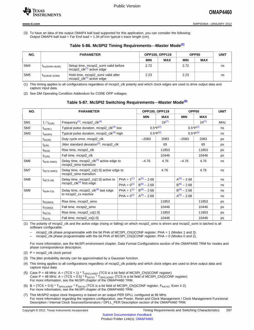
Public Version
OMAP4460
www.ti.com SWPS046A –JANUARY 2012
(3) To have an idea of the output OMAP4 ball load supported for this application, you can consider the following:Output OMAP4 ball load = Far End load + 1.34 pF/cm typical x trace length (cm).
Table 5-86. McSPI2 Timing Requirements—Master Mode(2)
NO. PARAMETER OPP100, OPP119 OPP50 UNIT
MIN MAX MIN MAX
SM4 tsu(SOMI-clkAE) Setup time, mcspi2_somi valid before 2.72 2.72 nsmcspi2_clk(1) active edge
SM5 th(clkAE-SOMI) Hold time, mcspi2_somi valid after 2.23 2.23 nsmcspi2_clk(1) active edge
(1) This timing applies to all configurations regardless of mcspi2_clk polarity and which clock edges are used to drive output data andcapture input data.
(2) See DM Operating Condition Addendum for CORE OPP voltages.
Table 5-87. McSPI2 Switching Requirements—Master Mode(8)
NO. PARAMETER OPP100, OPP119 OPP50 UNIT
MIN MAX MIN MAX
SM1 1 / tc(clk) Frequency(1), mcspi2_clk(4) 24(7) 24(7) MHz
SM2 tw(clkL) Typical pulse duration, mcspi2_clk(4) low 0.5*P(2) 0.5*P(2) ns
SM3 tw(clkH) Typical pulse duration, mcspi2_clk(4) high 0.5*P(2) 0.5*P(2) ns
tdc(clk) Duty cycle error, mcspi2_clk –2083 2083 –2083 2083 ps
tj(clk) Jitter standard deviation(3), mcspi2_clk 65 65 ps
tR(clk) Rise time, mcspi2_clk 11853 11853 ps
tF(clk) Fall time, mcspi2_clk 10446 10446 ps
SM6 td(clk-SIMO) Delay time, mcspi2_clk(4) active edge to –4.76 4.76 –4.76 4.76 nsmcspi2_simo transition
SM7 td(CS-SIMO) Delay time, mcspi2_cs[1:0] active edge to 4.76 4.76 nsmcspi2_simo transition
SM8 td(CS-clk) Delay time, mcspi2_cs[1:0] active to PHA = 1(1) A(5) – 2.68 A(5) – 2.68 nsmcspi2_clk(4) first edge PHA = 0(1) B(6) – 2.68 B(6) – 2.68 ns
SM9 td(clk-CS) Delay time, mcspi2_clk(4) last edge PHA = 1(1) B(6) – 2.68 B(6) – 2.68 nsto mcspi2_cs inactive PHA = 0(1) A(5) – 2.68 A(5) – 2.68 ns
tR(SIMO) Rise time, mcspi2_simo 11853 11853 ps
tF(SIMO) Fall time, mcspi2_simo 10446 10446 ps
tR(CS) Rise time, mcspi2_cs[1:0] 11853 11853 ps
tF(CS) Fall time, mcspi2_cs[1:0] 10446 10446 ps
(1) The polarity of mcspi2_clk and the active edge (rising or falling) on which mcspi2_simo is driven and mcspi2_somi is latched is allsoftware configurable:
– mcspi2_clk phase programmable with the bit PHA of MCSPI_Ch(i)CONF register: PHA = 1 (Modes 1 and 3).– mcspi2_clk phase programmable with the bit PHA of MCSPI_Ch(i)CONF register: PHA = 0 (Modes 0 and 2).
For more information, see the McSPI environment chapter, Data Format Configurations section of the OMAP4460 TRM for modes andphase correspondence description.
(2) P = mcspi2_clk clock period
(3) The jitter probability density can be approximated by a Gaussian function.
(4) This timing applies to all configurations regardless of mcspi2_clk polarity and which clock edges are used to drive output data andcapture input data.
(5) Case P = 48 MHz: A = (TCS + 1) * TSPICLKREF (TCS is a bit field of MCSPI_Ch(i)CONF register)Case P < 48 MHz: A = (TCS + 0.5) * FRATIO * TSPICLKREF (TCS is a bit field of MCSPI_Ch(i)CONF register)For more information, see the McSPI chapter of the OMAP4460 TRM.
(6) B = (TCS + 0.5) * TSPICLKREF * FRATIO (TCS is a bit field of MCSPI_Ch(i)CONF register, FRATIO: Even ≥ 2).For more information, see the McSPI chapter of the OMAP4460 TRM.
(7) This McSPI2 output clock frequency is based on an output PER DPLL configured at 96 MHz.For more information regarding the registers configuration, see Power, Reset and Clock Management / Clock Management FunctionalDescription / Internal Clock Sources/Generators / DPLL_PER Description section of the OMAP4460 TRM.
Copyright © 2012, Texas Instruments Incorporated Timing Requirements and Switching Characteristics 297Submit Documentation Feedback
Product Folder Link(s): OMAP4460
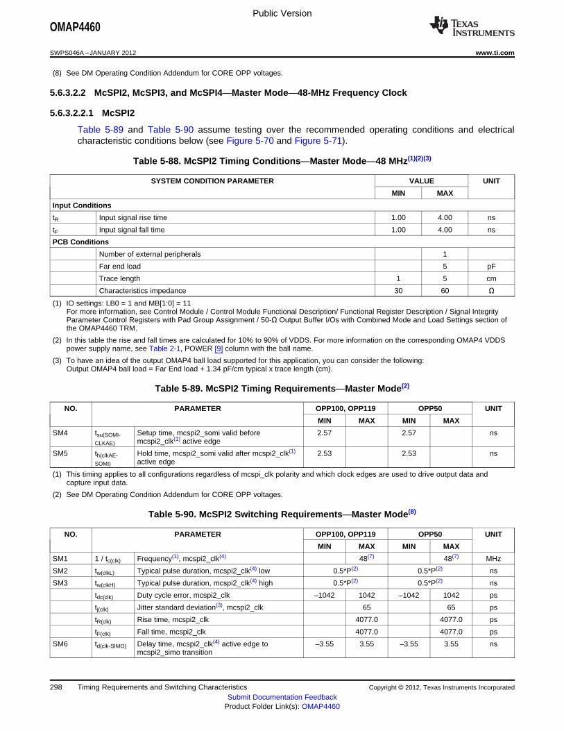
Public Version
OMAP4460
SWPS046A –JANUARY 2012 www.ti.com
(8) See DM Operating Condition Addendum for CORE OPP voltages.
5.6.3.2.2 McSPI2, McSPI3, and McSPI4—Master Mode—48-MHz Frequency Clock
5.6.3.2.2.1 McSPI2
Table 5-89 and Table 5-90 assume testing over the recommended operating conditions and electricalcharacteristic conditions below (see Figure 5-70 and Figure 5-71).
Table 5-88. McSPI2 Timing Conditions—Master Mode—48 MHz(1)(2)(3)
SYSTEM CONDITION PARAMETER VALUE UNIT
MIN MAX
Input Conditions
tR Input signal rise time 1.00 4.00 ns
tF Input signal fall time 1.00 4.00 ns
PCB Conditions
Number of external peripherals 1
Far end load 5 pF
Trace length 1 5 cm
Characteristics impedance 30 60 Ω
(1) IO settings: LB0 = 1 and MB[1:0] = 11For more information, see Control Module / Control Module Functional Description/ Functional Register Description / Signal IntegrityParameter Control Registers with Pad Group Assignment / 50-Ω Output Buffer I/Os with Combined Mode and Load Settings section ofthe OMAP4460 TRM.
(2) In this table the rise and fall times are calculated for 10% to 90% of VDDS. For more information on the corresponding OMAP4 VDDSpower supply name, see Table 2-1, POWER [9] column with the ball name.
(3) To have an idea of the output OMAP4 ball load supported for this application, you can consider the following:Output OMAP4 ball load = Far End load + 1.34 pF/cm typical x trace length (cm).
Table 5-89. McSPI2 Timing Requirements—Master Mode(2)
NO. PARAMETER OPP100, OPP119 OPP50 UNIT
MIN MAX MIN MAX
SM4 tsu(SOMI- Setup time, mcspi2_somi valid before 2.57 2.57 nsCLKAE) mcspi2_clk(1) active edge
SM5 th(clkAE- Hold time, mcspi2_somi valid after mcspi2_clk(1) 2.53 2.53 nsSOMI) active edge
(1) This timing applies to all configurations regardless of mcspi_clk polarity and which clock edges are used to drive output data andcapture input data.
(2) See DM Operating Condition Addendum for CORE OPP voltages.
Table 5-90. McSPI2 Switching Requirements—Master Mode(8)
NO. PARAMETER OPP100, OPP119 OPP50 UNIT
MIN MAX MIN MAX
SM1 1 / tc(clk) Frequency(1), mcspi2_clk(4) 48(7) 48(7) MHz
SM2 tw(clkL) Typical pulse duration, mcspi2_clk(4) low 0.5*P(2) 0.5*P(2) ns
SM3 tw(clkH) Typical pulse duration, mcspi2_clk(4) high 0.5*P(2) 0.5*P(2) ns
tdc(clk) Duty cycle error, mcspi2_clk –1042 1042 –1042 1042 ps
tj(clk) Jitter standard deviation(3), mcspi2_clk 65 65 ps
tR(clk) Rise time, mcspi2_clk 4077.0 4077.0 ps
tF(clk) Fall time, mcspi2_clk 4077.0 4077.0 ps
SM6 td(clk-SIMO) Delay time, mcspi2_clk(4) active edge to –3.55 3.55 –3.55 3.55 nsmcspi2_simo transition
298 Timing Requirements and Switching Characteristics Copyright © 2012, Texas Instruments Incorporated
Submit Documentation FeedbackProduct Folder Link(s): OMAP4460
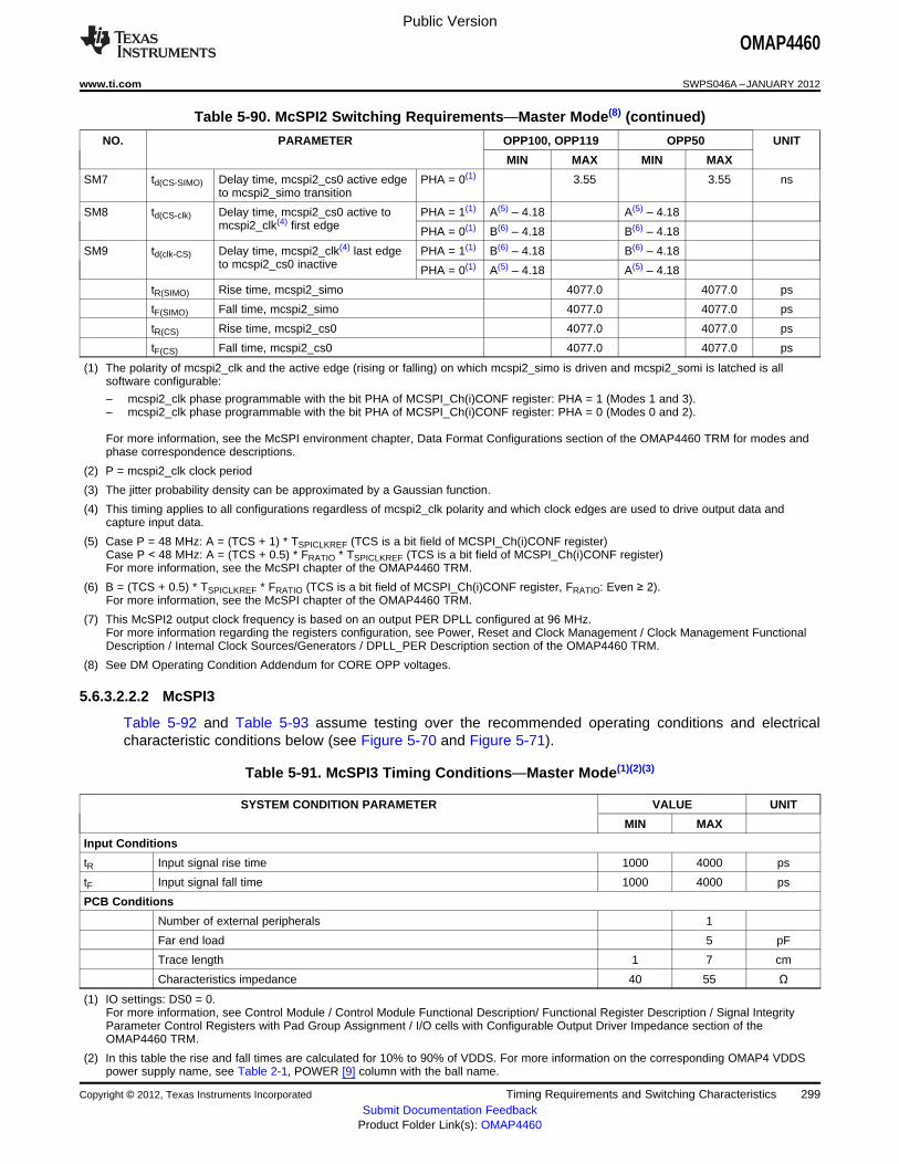
Public Version
OMAP4460
www.ti.com SWPS046A –JANUARY 2012
Table 5-90. McSPI2 Switching Requirements—Master Mode(8) (continued)
NO. PARAMETER OPP100, OPP119 OPP50 UNIT
MIN MAX MIN MAX
SM7 td(CS-SIMO) Delay time, mcspi2_cs0 active edge PHA = 0(1) 3.55 3.55 nsto mcspi2_simo transition
SM8 td(CS-clk) Delay time, mcspi2_cs0 active to PHA = 1(1) A(5) – 4.18 A(5) – 4.18mcspi2_clk(4) first edge PHA = 0(1) B(6) – 4.18 B(6) – 4.18
SM9 td(clk-CS) Delay time, mcspi2_clk(4) last edge PHA = 1(1) B(6) – 4.18 B(6) – 4.18to mcspi2_cs0 inactive PHA = 0(1) A(5) – 4.18 A(5) – 4.18
tR(SIMO) Rise time, mcspi2_simo 4077.0 4077.0 ps
tF(SIMO) Fall time, mcspi2_simo 4077.0 4077.0 ps
tR(CS) Rise time, mcspi2_cs0 4077.0 4077.0 ps
tF(CS) Fall time, mcspi2_cs0 4077.0 4077.0 ps
(1) The polarity of mcspi2_clk and the active edge (rising or falling) on which mcspi2_simo is driven and mcspi2_somi is latched is allsoftware configurable:
– mcspi2_clk phase programmable with the bit PHA of MCSPI_Ch(i)CONF register: PHA = 1 (Modes 1 and 3).– mcspi2_clk phase programmable with the bit PHA of MCSPI_Ch(i)CONF register: PHA = 0 (Modes 0 and 2).
For more information, see the McSPI environment chapter, Data Format Configurations section of the OMAP4460 TRM for modes andphase correspondence descriptions.
(2) P = mcspi2_clk clock period
(3) The jitter probability density can be approximated by a Gaussian function.
(4) This timing applies to all configurations regardless of mcspi2_clk polarity and which clock edges are used to drive output data andcapture input data.
(5) Case P = 48 MHz: A = (TCS + 1) * TSPICLKREF (TCS is a bit field of MCSPI_Ch(i)CONF register)Case P < 48 MHz: A = (TCS + 0.5) * FRATIO * TSPICLKREF (TCS is a bit field of MCSPI_Ch(i)CONF register)For more information, see the McSPI chapter of the OMAP4460 TRM.
(6) B = (TCS + 0.5) * TSPICLKREF * FRATIO (TCS is a bit field of MCSPI_Ch(i)CONF register, FRATIO: Even ≥ 2).For more information, see the McSPI chapter of the OMAP4460 TRM.
(7) This McSPI2 output clock frequency is based on an output PER DPLL configured at 96 MHz.For more information regarding the registers configuration, see Power, Reset and Clock Management / Clock Management FunctionalDescription / Internal Clock Sources/Generators / DPLL_PER Description section of the OMAP4460 TRM.
(8) See DM Operating Condition Addendum for CORE OPP voltages.
5.6.3.2.2.2 McSPI3
Table 5-92 and Table 5-93 assume testing over the recommended operating conditions and electricalcharacteristic conditions below (see Figure 5-70 and Figure 5-71).
Table 5-91. McSPI3 Timing Conditions—Master Mode(1)(2)(3)
SYSTEM CONDITION PARAMETER VALUE UNIT
MIN MAX
Input Conditions
tR Input signal rise time 1000 4000 ps
tF Input signal fall time 1000 4000 ps
PCB Conditions
Number of external peripherals 1
Far end load 5 pF
Trace length 1 7 cm
Characteristics impedance 40 55 Ω
(1) IO settings: DS0 = 0.For more information, see Control Module / Control Module Functional Description/ Functional Register Description / Signal IntegrityParameter Control Registers with Pad Group Assignment / I/O cells with Configurable Output Driver Impedance section of theOMAP4460 TRM.
(2) In this table the rise and fall times are calculated for 10% to 90% of VDDS. For more information on the corresponding OMAP4 VDDSpower supply name, see Table 2-1, POWER [9] column with the ball name.
Copyright © 2012, Texas Instruments Incorporated Timing Requirements and Switching Characteristics 299Submit Documentation Feedback
Product Folder Link(s): OMAP4460

Public Version
OMAP4460
SWPS046A –JANUARY 2012 www.ti.com
(3) To have an idea of the output OMAP4 ball load supported for this application, you can consider the following:Output OMAP4 ball load = Far End load + 1.34 pF/cm typical x trace length (cm).
Table 5-92. McSPI3 Timing Requirements—Master Mode(2)
NO. PARAMETER OPP100, OPP119 OPP50 UNIT
MIN MAX MIN MAX
SM4 tsu(SOMI-CLKAE) Setup time, mcspi3_somi valid before 2.29 2.29 nsmcspi3_clk(1) active edge
SM5 th(clkAE-SOMI) Hold time, mcspi3_somi valid after 2.67 2.67 nsmcspi3_clk(1) active edge
(1) This timing applies to all configurations regardless of mcspi_clk polarity and which clock edges are used to drive output data andcapture input data.
(2) See DM Operating Condition Addendum for CORE OPP voltages.
Table 5-93. McSPI3 Switching Requirements—Master Mode(8)
NO. PARAMETER OPP100, OPP119 OPP50 UNIT
MIN MAX MIN MAX
SM1 1 / tc(clk) Frequency(1), mcspi3_clk(4) 48(7) 48(7) MHz
SM2 tw(clkL) Typical pulse duration, mcspi3_clk(4) low 0.5*P(2) 0.5*P(2) ns
SM3 tw(clkH) Typical pulse duration, mcspi3_clk(4) high 0.5*P(2) 0.5*P(2) ns
tdc(clk) Duty cycle error, mcspi3_clk –1042 1042 –1042 1042 ps
tj(clk) Jitter standard deviation(3), mcspi3_clk 65 65 ps
tR(clk) Rise time, mcspi3_clk 3820.4 3820.4 ps
tF(clk) Fall time, mcspi3_clk 3442.4 3442.4 ps
SM6 td(clk-SIMO) Delay time, mcspi3_clk(4) active edge to –3.57 3.57 –3.57 3.57 nsmcspi3_simo transition
SM7 td(CS-SIMO) Delay time, mcspi3_cs0 active edge to 3.57 3.57 nsmcspi3_simo transition
SM8 td(CS-clk) Delay time, mcspi3_cs0 active to PHA = 1(1) A(5) – 4.2 A(5) – 4.2 nsmcspi3_clk(4) first edge PHA = 0(1) B(6) – 4.2 B(6) – 4.2 ns
SM9 td(clk-CS) Delay time, mcspi3_clk(4) last edge PHA = 1(1) B(6) – 4.2 B(6) – 4.2 nsto mcspi3_cs0 inactive PHA = 0(1) A(5) – 4.2 A(5) – 4.2 ns
tR(SIMO) Rise time, mcspi3_simo 3820.4 3820.4 ps
tF(SIMO) Fall time, mcspi3_simo 3442.4 3442.4 ps
tR(CS) Rise time, mcspi3_cs0 3820.4 3820.4 ps
tF(CS) Fall time, mcspi3_cs0 3442.4 3442.4 ps
(1) The polarity of mcspi3_clk and the active edge (rising or falling) on which mcspi3_simo is driven and mcspi3_somi is latched is allsoftware configurable:
– mcspi3_clk phase programmable with the bit PHA of MCSPI_Ch(i)CONF register: PHA = 1 (Modes 1 and 3).– mcspi3_clk phase programmable with the bit PHA of MCSPI_Ch(i)CONF register: PHA = 0 (Modes 0 and 2).
For more information, see the McSPI environment chapter, Data Format Configurations section of the OMAP4460 TRM for modes andphase correspondence descriptions.
(2) P = mcspi3_clk clock period
(3) The jitter probability density can be approximated by a Gaussian function.
(4) This timing applies to all configurations regardless of mcspi3_clk polarity and which clock edges are used to drive output data andcapture input data.
(5) Case P = 48 MHz: A = (TCS + 1) * TSPICLKREF (TCS is a bit field of MCSPI_Ch(i)CONF register)Case P < 48 MHz: A = (TCS + 0.5) * FRATIO * TSPICLKREF (TCS is a bit field of MCSPI_Ch(i)CONF register)For more information, see the McSPI chapter of the OMAP4460 TRM.
(6) B = (TCS + 0.5) * TSPICLKREF * FRATIO (TCS is a bit field of MCSPI_Ch(i)CONF register, FRATIO: Even ≥ 2).For more information, see the McSPI chapter of the OMAP4460 TRM.
(7) This McSPI3 output clock frequency is based on an output PER DPLL configured at 96 MHz.For more information regarding the registers configuration, see Power, Reset and Clock Management / Clock Management FunctionalDescription / Internal Clock Sources/Generators / DPLL_PER Description section of the OMAP4460 TRM.
300 Timing Requirements and Switching Characteristics Copyright © 2012, Texas Instruments Incorporated
Submit Documentation FeedbackProduct Folder Link(s): OMAP4460
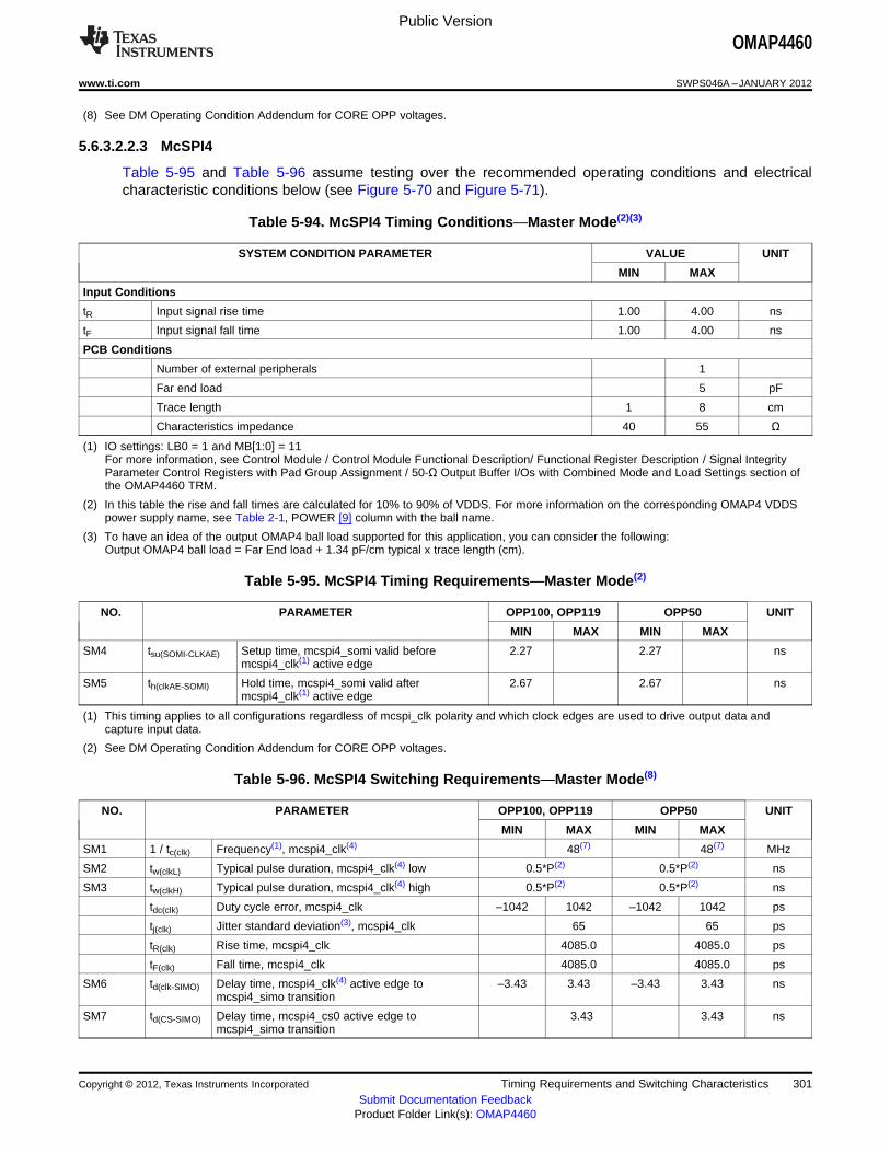
Public Version
OMAP4460
www.ti.com SWPS046A –JANUARY 2012
(8) See DM Operating Condition Addendum for CORE OPP voltages.
5.6.3.2.2.3 McSPI4
Table 5-95 and Table 5-96 assume testing over the recommended operating conditions and electricalcharacteristic conditions below (see Figure 5-70 and Figure 5-71).
Table 5-94. McSPI4 Timing Conditions—Master Mode(2)(3)
SYSTEM CONDITION PARAMETER VALUE UNIT
MIN MAX
Input Conditions
tR Input signal rise time 1.00 4.00 ns
tF Input signal fall time 1.00 4.00 ns
PCB Conditions
Number of external peripherals 1
Far end load 5 pF
Trace length 1 8 cm
Characteristics impedance 40 55 Ω
(1) IO settings: LB0 = 1 and MB[1:0] = 11For more information, see Control Module / Control Module Functional Description/ Functional Register Description / Signal IntegrityParameter Control Registers with Pad Group Assignment / 50-Ω Output Buffer I/Os with Combined Mode and Load Settings section ofthe OMAP4460 TRM.
(2) In this table the rise and fall times are calculated for 10% to 90% of VDDS. For more information on the corresponding OMAP4 VDDSpower supply name, see Table 2-1, POWER [9] column with the ball name.
(3) To have an idea of the output OMAP4 ball load supported for this application, you can consider the following:Output OMAP4 ball load = Far End load + 1.34 pF/cm typical x trace length (cm).
Table 5-95. McSPI4 Timing Requirements—Master Mode(2)
NO. PARAMETER OPP100, OPP119 OPP50 UNIT
MIN MAX MIN MAX
SM4 tsu(SOMI-CLKAE) Setup time, mcspi4_somi valid before 2.27 2.27 nsmcspi4_clk(1) active edge
SM5 th(clkAE-SOMI) Hold time, mcspi4_somi valid after 2.67 2.67 nsmcspi4_clk(1) active edge
(1) This timing applies to all configurations regardless of mcspi_clk polarity and which clock edges are used to drive output data andcapture input data.
(2) See DM Operating Condition Addendum for CORE OPP voltages.
Table 5-96. McSPI4 Switching Requirements—Master Mode(8)
NO. PARAMETER OPP100, OPP119 OPP50 UNIT
MIN MAX MIN MAX
SM1 1 / tc(clk) Frequency(1), mcspi4_clk(4) 48(7) 48(7) MHz
SM2 tw(clkL) Typical pulse duration, mcspi4_clk(4) low 0.5*P(2) 0.5*P(2) ns
SM3 tw(clkH) Typical pulse duration, mcspi4_clk(4) high 0.5*P(2) 0.5*P(2) ns
tdc(clk) Duty cycle error, mcspi4_clk –1042 1042 –1042 1042 ps
tj(clk) Jitter standard deviation(3), mcspi4_clk 65 65 ps
tR(clk) Rise time, mcspi4_clk 4085.0 4085.0 ps
tF(clk) Fall time, mcspi4_clk 4085.0 4085.0 ps
SM6 td(clk-SIMO) Delay time, mcspi4_clk(4) active edge to –3.43 3.43 –3.43 3.43 nsmcspi4_simo transition
SM7 td(CS-SIMO) Delay time, mcspi4_cs0 active edge to 3.43 3.43 nsmcspi4_simo transition
Copyright © 2012, Texas Instruments Incorporated Timing Requirements and Switching Characteristics 301Submit Documentation Feedback
Product Folder Link(s): OMAP4460

Public Version
OMAP4460
SWPS046A –JANUARY 2012 www.ti.com
Table 5-96. McSPI4 Switching Requirements—Master Mode(8) (continued)
NO. PARAMETER OPP100, OPP119 OPP50 UNIT
MIN MAX MIN MAX
SM8 td(CS-clk) Delay time, mcspi4_cs0 active to PHA = 1(1) A(5) – 4.06 A(5) – 4.06 nsmcspi4_clk(4) first edge PHA = 0(1) B(6) – 4.06 B(6) – 4.06 ns
SM9 td(clk-CS) Delay time, mcspi4_clk(4) last edge PHA = 1(1) B(6) – 4.06 B(6) – 4.06 nsto mcspi4_cs inactive PHA = 0(1) A(5) – 4.06 A(5) – 4.06 ns
tR(SIMO) Rise time, mcspi4_simo 4085.0 4085.0 ps
tF(SIMO) Fall time, mcspi4_simo 4085.0 4085.0 ps
tR(CS) Rise time, mcspi4_cs0 4085.0 4085.0 ps
tF(CS) Fall time, mcspi4_cs0 4085.0 4085.0 ps
(1) The polarity of mcspi4_clk and the active edge (rising or falling) on which mcspi4_simo is driven and mcspi4_somi is latched is allsoftware configurable:
– mcspi4_clk phase programmable with the bit PHA of MCSPI_Ch(i)CONF register: PHA = 1 (Modes 1 and 3).– mcspi4_clk phase programmable with the bit PHA of MCSPI_Ch(i)CONF register: PHA = 0 (Modes 0 and 2).
For more information, see the McSPI environment chapter, Data Format Configurations section of the OMAP4460 TRM for modes andphase correspondence descriptions.
(2) P = mcspi4_clk clock period
(3) The jitter probability density can be approximated by a Gaussian function.
(4) This timing applies to all configurations regardless of mcspi4_clk polarity and which clock edges are used to drive output data andcapture input data.
(5) Case P = 48 MHz: A = (TCS + 1) * TSPICLKREF (TCS is a bit field of MCSPI_Ch(i)CONF register)Case P < 48 MHz: A = (TCS + 0.5) * FRATIO * TSPICLKREF (TCS is a bit field of MCSPI_Ch(i)CONF register)For more information, see the McSPI chapter of the OMAP4460 TRM.
(6) B = (TCS + 0.5) * TSPICLKREF * FRATIO (TCS is a bit field of MCSPI_Ch(i)CONF register, FRATIO: Even ≥ 2).For more information, see the McSPI chapter of the OMAP4460 TRM.
(7) This McSPI4 output clock frequency is based on an output PER DPLL configured at 96 MHz.For more information regarding the registers configuration, see Power, Reset and Clock Management / Clock Management FunctionalDescription / Internal Clock Sources/Generators / DPLL_PER Description section of the OMAP4460 TRM.
(8) See DM Operating Condition Addendum for CORE OPP voltages.
302 Timing Requirements and Switching Characteristics Copyright © 2012, Texas Instruments Incorporated
Submit Documentation FeedbackProduct Folder Link(s): OMAP4460
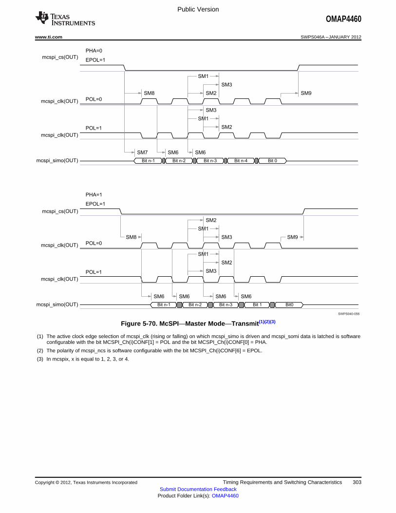
mcspi_cs(OUT)
mcspi_clk(OUT)
mcspi_clk(OUT)
mcspi_simo(OUT)
mcspi_cs(OUT)
mcspi_clk(OUT)
mcspi_clk(OUT)
mcspi_simo(OUT)
Bit n-1 Bit n-2 Bit n-3 Bit n-4 Bit 0
Bit n-1 Bit n-2 Bit n-3 Bit 1 Bit0
PHA=0
EPOL=1
POL=0
POL=1
PHA=1
EPOL=1
POL=0
POL=1
SM8 SM9
SM6
SM3
SM1
SM2
SM1
SM8 SM9SM3
SM1
SM2
SM1
SM6
SM7 SM6
SM2
SM3
SM2
SM3
SM6 SM6 SM6
SWPS040-056
Public Version
OMAP4460
www.ti.com SWPS046A –JANUARY 2012
Figure 5-70. McSPI—Master Mode—Transmit(1)(2)(3)
(1) The active clock edge selection of mcspi_clk (rising or falling) on which mcspi_simo is driven and mcspi_somi data is latched is softwareconfigurable with the bit MCSPI_Ch(i)CONF[1] = POL and the bit MCSPI_Ch(i)CONF[0] = PHA.
(2) The polarity of mcspi_ncs is software configurable with the bit MCSPI_Ch(i)CONF[6] = EPOL.
(3) In mcspix, x is equal to 1, 2, 3, or 4.
Copyright © 2012, Texas Instruments Incorporated Timing Requirements and Switching Characteristics 303Submit Documentation Feedback
Product Folder Link(s): OMAP4460
mcspi_cs(OUT)
mcspi_clk(OUT)
mcspi_clk(OUT)
mcspi_somi(IN)
mcspi_cs(OUT)
mcspi_clk(OUT)
mcspi_clk(OUT)
mcspi_somi(IN)
Bit n-1 Bit n-2 Bit n-3 Bit n-4 Bit 0
Bit n-1 Bit n-2 Bit n-3 Bit 1 Bit 0
PHA=0
EPOL=1
PHA=1
EPOL=1
POL=0
POL=1
POL=0
POL=1
SM8 SM9
SM3
SM1
SM2
SM1
SM8 SM9SM3
SM1
SM2
SM1
SM2
SM3
SM2
SM3
SM5 SM5
SM5 SM5
SM4 SM4
SM4 SM4
SWPS040-057
Public Version
OMAP4460
SWPS046A –JANUARY 2012 www.ti.com
Figure 5-71. McSPI—Master Mode—Transmit(1)(2)(3)
(1) The active clock edge selection of mcspi_clk (rising or falling) on which mcspi_simo is driven and mcspi_somi data is latched is softwareconfigurable with the bit MCSPI_Ch(i)CONF[1] = POL and the bit MCSPI_Ch(i)CONF[0] = PHA.
(2) The polarity of mcspi_ncs is software configurable with the bit MCSPI_Ch(i)CONF[6] = EPOL.
(3) In mcspix, x is equal to 1, 2, 3, or 4.
304 Timing Requirements and Switching Characteristics Copyright © 2012, Texas Instruments Incorporated
Submit Documentation FeedbackProduct Folder Link(s): OMAP4460

Public Version
OMAP4460
www.ti.com SWPS046A –JANUARY 2012
5.6.4 Digital Microphone (DMIC)
NOTEFor more information, see the Digital Microphone Controller chapter in the OMAP4460 TRM.
The DMIC allows support of up to three digital stereo microphones that send it a pulse-density modulatedstream of bits, transferred on one period or one half-period of the clock (over-sampling clock) provided tothe DMIC.
Table 5-98 and Table 5-99 assume testing over the recommended operating conditions and electricalcharacteristic conditions below (see Figure 5-73).
Table 5-97. DMIC Timing Conditions—Master/Receive Mode(1)(2)(4)
TIMING CONDITION PARAMETER VALUE UNIT
MIN MAX
Input Conditions
tR Input signal rise time 10 ns
tF Input signal fall time 10 ns
PCB Conditions (3)
Number of external peripherals See(5)
Far end load when accounting for external ESD protection 20 pF
Trace length 25 cm
Characteristics impedance 40 70 Ω
(1) IO settings: LB0 = 0 and MB[1:0] = 10
– For balls AE24 / AF24 / AG24 / AH24 (abe_dmic_clk1 / abe_dmic_din1 / abe_dmic_din2 / abe_dmic_din3 in multiplexing mode 0),for more information see Control Module / Control Module Functional Description/ Functional Register Description / Signal IntegrityParameter Control Registers with Pad Group Assignment / 50-Ω Output Buffer I/Os with Combined Mode and Load Settings sectionof the OMAP4460 TRM.
– For balls AF16 / AG16 (abe_dmic_din3 / abe_dmic_clk3 in multiplexing mode 5), see Control Module / Control Module FunctionalDescription/ Functional Register Description / Signal Integrity Parameter Control Registers with Pad Group Assignment / I/Os withCombined Mode and Load Settings section of the OMAP4460 TRM.
(2) In this table the rise and fall times are calculated for 20% to 80% of VDDS. For more information on the corresponding OMAP4 VDDSpower supply name, see Table 2-1, POWER [9] column with the ball name.
(3) Figure 5-72 shows an example of DMIC implementation.
(4) To have an idea of the output OMAP4 ball load supported for this application, you can consider the following:Output OMAP4 ball load = Far End load + 1.34 pF/cm typical x trace length (cm).
(5) For more information on the peripheral conditions, see Figure 5-72, DMIC Implementation Example.
Copyright © 2012, Texas Instruments Incorporated Timing Requirements and Switching Characteristics 305Submit Documentation Feedback
Product Folder Link(s): OMAP4460
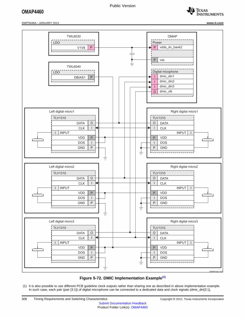
Left digital micro1
TLV1310
DATA
CLK
INPUT
VDD
DOS
GND
I
O
I
P
I
P
Right digital micro1
O
I
P
I
P
DATA
CLK
VDD
DOS
GND
IINPUT
TWL6030
V1V8 P
LDO
DBIAS1
LDO
P
TWL6040
vdds_dv_bank2P
vss
dmic_din1
dmic_din2
dmic_din3
dmic_clk
P
O
I
I
I
TLV1310
Left digital micro2
TLV1310
DATA
CLK
INPUT
VDD
DOS
GND
I
O
I
P
I
P
Right digital micro2
O
I
P
I
P
DATA
CLK
VDD
DOS
GND
IINPUT
TLV1310
Left digital micro3
TLV1310
DATA
CLK
INPUT
VDD
DOS
GND
I
O
I
P
I
P
Right digital micro3
O
I
P
I
P
DATA
CLK
VDD
DOS
GND
IINPUT
TLV1310
OMAP
I
Digital micophone
SWPS040-202
Power
Public Version
OMAP4460
SWPS046A –JANUARY 2012 www.ti.com
Figure 5-72. DMIC Implementation Example(1)
(1) It is also possible to use different PCB guideline clock outputs rather than sharing one as described in above implementation example.In such case, each pair (pair [3:1]) of digital microphone can be connected to a dedicated data and clock signals (dmic_din[3:1],
306 Timing Requirements and Switching Characteristics Copyright © 2012, Texas Instruments Incorporated
Submit Documentation FeedbackProduct Folder Link(s): OMAP4460
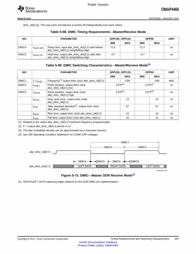
SWPS040-058
abe_dmic_clk[3:1]
abe_dmic_din[3:1] LEFT DATA RIGHT DATA LEFT DATA
DMIC2
DMIC1
DMIC3
DMIC4 DMIC4DMIC5 DMIC5
Public Version
OMAP4460
www.ti.com SWPS046A –JANUARY 2012
dmic_clk[3:1]). This way each microphone is turned off independently from each others.
Table 5-98. DMIC Timing Requirements—Master/Receive Mode
NO. PARAMETER OPP100, OPP119 OPP50 UNIT
MIN MAX MIN MAX
DMIC4 tsu(dV-clkH) Setup time, input abe_dmic_din[3:1] valid before 72.3 72.3 nsabe_dmic_clk[3:1] rising/falling edge
DMIC5 th(clkH-dV) Hold time, output abe_dmic_din[3:1] valid after –0.7 –0.7 nsabe_dmic_clk[3:1] rising/falling edge
Table 5-99. DMIC Switching Characteristics—Master/Receive Mode(4)
NO. PARAMETER OPP100, OPP119 OPP50 UNIT
MIN MAX MIN MAX
DMIC1 1 / tc(clk) Frequency(1) output dmic clock abe_dmic_clk[3:1] 3.84 3.84 MHz
DMIC2 tw(clkL) Pulse duration, output dmic clock 0.5*P(2) 0.5*P(2) nsabe_dmic_clk[3:1] low
DMIC3 tw(clkH) Pulse duration, output dmic clock 0.5*P(2) 0.5*P(2) nsabe_dmic_clk[3:1] high
tdc(clk) Duty cycle error, output dmic clock 13 13 nsabe_dmic_clk[3:1]
tj(clk) Jitter standard deviation(3), output dmic clock 67 67 nsabe_dmic_clk[3:1]
tR(clk) Rise time, output dmic clock abe_dmic_clk[3:1] 10 10 ns
tF(clk) Fall time, output dmic clock abe_dmic_clk[3:1] 10 10 ns
(1) Related to the output abe_dmic_clk[3:1] maximum frequency programmable.
(2) P = output abe_dmic_clk[3:1] period in ns
(3) The jitter probability density can be approximated by a Gaussian function.
(4) See DM Operating Condition Addendum for CORE OPP voltages.
Figure 5-73. DMIC—Master DDR Receive Mode(1)
(1) RIGHT/LEFT DATA capturing edges depend on the DOS DMIC pin implementation.
Copyright © 2012, Texas Instruments Incorporated Timing Requirements and Switching Characteristics 307Submit Documentation Feedback
Product Folder Link(s): OMAP4460

Public Version
OMAP4460
SWPS046A –JANUARY 2012 www.ti.com
5.6.5 Multichannel Pulse Density Modulation (McPDM)
Multichannel pulse density modulation interface (McPDM) is an audio module dedicated to mobiletelephone terminal. It’s composed of uplink and downlink paths both communicating with audio companionchip through a dedicated interface. Aim of the uplink path is to process data from the McPDM interface,decimate and filter the data, and store them in FIFO. FIFO will be controlled by IRQ or DMA request andfed outside from McPDM module following standard OCP format.
Aim of the downlink path is to process data coming from FIFO, through sigma-delta converter and feed itto McPDM interface. The data is also transmitted to audio companion chip by operating a samplefrequency conversion.
Table 5-101 and Table 5-102 assume testing over the recommended operating conditions and electricalcharacteristic conditions below (see Figure 5-74 and Figure 5-75).
Table 5-100. McPDM Timing Conditions(1)(2)(3)
SYSTEM CONDITION PARAMETER VALUE UNIT
MIN MAX
Input Conditions
tR Input signal rise time 1.00 6.00 ns
tF Input signal fall time 1.00 6.00 ns
PCB Conditions
Number of external peripherals 1
Far end load 5 pF
Trace length 5 cm
Characteristics impedance 20 65 Ω
(1) IO settings: MB[1:0]= 01 and LB0 = 0For more information, see Control Module / Control Module Functional Description/ Functional Register Description / Signal IntegrityParameter Control Registers with Pad Group Assignment / 50-Ω Output Buffer I/Os with Combined Mode and Load Settings section ofthe OMAP4460 TRM.
(2) In this table the rise and fall times are calculated for 10% to 90% of VDDS. For more information on the corresponding OMAP4 VDDSpower supply name, see Table 2-1, POWER [9] column with the ball name.
(3) To have an idea of the output OMAP4 ball load supported for this application, you can consider the following:Output OMAP4 ball load = Far End load + 1.34 pF/cm typical x trace length (cm).
Table 5-101. McPDM Timing Requirements—Master and Receive SDR Mode(3)
NO. PARAMETER OPP100, OPP119 OPP50 UNIT
MIN MAX MIN MAX
fc(clks) Input abe_clks(2) frequency 19.2(2) 19.2(2) MHz
tw(clksL) Typical pulse duration, input abe_clks low 0.5 * P(1) 0.5 * P(1) ns
tw(clksH) Typical pulse duration, output abe_clks high 0.5 * P(1) 0.5 * P(1) ns
tdc(clks) Duty cycle error, input abe_clks –0.05 * P(1) 0.05 * P(1) – –0.05 * P(1) 0.05 * P(1) – ps+ 1450 1450 + 1450 1450
tj(clks) Jitter peak to peak, input abe_clks 300 300 ps
PDM6 tsu(ulV-clkH) Setup time, abe_pdm_ul_data valid before 21.68 21.68 nsabe_pdm_lb_clk rising edge
PDM7 th(clkH-ulV) Hold time, abe_pdm_ul_data valid after 0.10 0.10 nsabe_pdm_lb_clk rising edge
PDM8 tsu(frameV-clkH) Setup time, abe_pdm_frame valid before 21.68 21.68 nsabe_pdm_lb_clk rising edge
PDM9 th(clkH-frameV) Hold time, abe_pdm_frame valid after 0.10 0.10 nsabe_pdm_lb_clk rising edge
308 Timing Requirements and Switching Characteristics Copyright © 2012, Texas Instruments Incorporated
Submit Documentation FeedbackProduct Folder Link(s): OMAP4460
Public Version
OMAP4460
www.ti.com SWPS046A –JANUARY 2012
(1) P = abe_clks input clock period in ns
(2) The McBSP (interface 1, 2, or 3) can be used at the same time with McPDM one. In this case, abe_clks clock is shared, that meansidentical, between McPDM and McBSP. As a consequence, the minimum clock frequency between McPDM and McBSP, input jitter, andduty cycle must be considered between both interfaces.
(3) See DM Operating Condition Addendum for CORE OPP voltages.
Copyright © 2012, Texas Instruments Incorporated Timing Requirements and Switching Characteristics 309Submit Documentation Feedback
Product Folder Link(s): OMAP4460
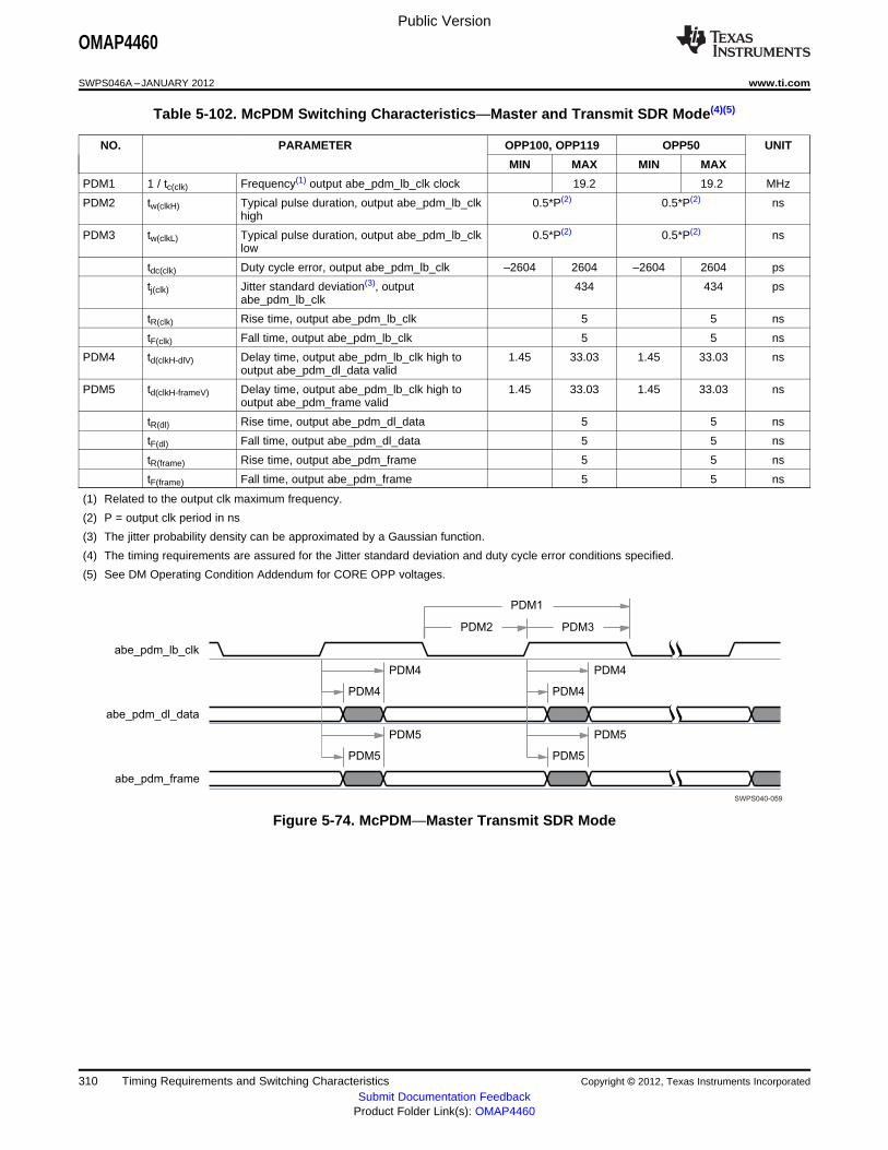
SWPS040-059
abe_pdm_lb_clk
abe_pdm_dl_data
abe_pdm_frame
PDM2
PDM1
PDM3
PDM4
PDM4
PDM4
PDM4
PDM5
PDM5
PDM5
PDM5
Public Version
OMAP4460
SWPS046A –JANUARY 2012 www.ti.com
Table 5-102. McPDM Switching Characteristics—Master and Transmit SDR Mode(4)(5)
NO. PARAMETER OPP100, OPP119 OPP50 UNIT
MIN MAX MIN MAX
PDM1 1 / tc(clk) Frequency(1) output abe_pdm_lb_clk clock 19.2 19.2 MHz
PDM2 tw(clkH) Typical pulse duration, output abe_pdm_lb_clk 0.5*P(2) 0.5*P(2) nshigh
PDM3 tw(clkL) Typical pulse duration, output abe_pdm_lb_clk 0.5*P(2) 0.5*P(2) nslow
tdc(clk) Duty cycle error, output abe_pdm_lb_clk –2604 2604 –2604 2604 ps
tj(clk) Jitter standard deviation(3), output 434 434 psabe_pdm_lb_clk
tR(clk) Rise time, output abe_pdm_lb_clk 5 5 ns
tF(clk) Fall time, output abe_pdm_lb_clk 5 5 ns
PDM4 td(clkH-dlV) Delay time, output abe_pdm_lb_clk high to 1.45 33.03 1.45 33.03 nsoutput abe_pdm_dl_data valid
PDM5 td(clkH-frameV) Delay time, output abe_pdm_lb_clk high to 1.45 33.03 1.45 33.03 nsoutput abe_pdm_frame valid
tR(dl) Rise time, output abe_pdm_dl_data 5 5 ns
tF(dl) Fall time, output abe_pdm_dl_data 5 5 ns
tR(frame) Rise time, output abe_pdm_frame 5 5 ns
tF(frame) Fall time, output abe_pdm_frame 5 5 ns
(1) Related to the output clk maximum frequency.
(2) P = output clk period in ns
(3) The jitter probability density can be approximated by a Gaussian function.
(4) The timing requirements are assured for the Jitter standard deviation and duty cycle error conditions specified.
(5) See DM Operating Condition Addendum for CORE OPP voltages.
Figure 5-74. McPDM—Master Transmit SDR Mode
310 Timing Requirements and Switching Characteristics Copyright © 2012, Texas Instruments Incorporated
Submit Documentation FeedbackProduct Folder Link(s): OMAP4460
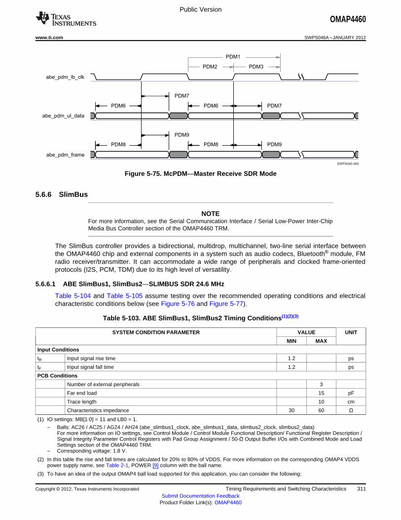
SWPS040-060
abe_pdm_lb_clk
abe_pdm_ul_data
abe_pdm_frame
PDM2
PDM1
PDM3
PDM6 PDM7
PDM7
PDM6
PDM8 PDM8
PDM9
PDM9
Public Version
OMAP4460
www.ti.com SWPS046A –JANUARY 2012
Figure 5-75. McPDM—Master Receive SDR Mode
5.6.6 SlimBus
NOTEFor more information, see the Serial Communication Interface / Serial Low-Power Inter-ChipMedia Bus Controller section of the OMAP4460 TRM.
The SlimBus controller provides a bidirectional, multidrop, multichannel, two-line serial interface betweenthe OMAP4460 chip and external components in a system such as audio codecs, Bluetooth® module, FMradio receiver/transmitter. It can accommodate a wide range of peripherals and clocked frame-orientedprotocols (I2S, PCM, TDM) due to its high level of versatility.
5.6.6.1 ABE SlimBus1, SlimBus2—SLIMBUS SDR 24.6 MHz
Table 5-104 and Table 5-105 assume testing over the recommended operating conditions and electricalcharacteristic conditions below (see Figure 5-76 and Figure 5-77).
Table 5-103. ABE SlimBus1, SlimBus2 Timing Conditions(1)(2)(3)
SYSTEM CONDITION PARAMETER VALUE UNIT
MIN MAX
Input Conditions
tR Input signal rise time 1.2 ps
tF Input signal fall time 1.2 ps
PCB Conditions
Number of external peripherals 3
Far end load 15 pF
Trace length 10 cm
Characteristics impedance 30 60 Ω
(1) IO settings: MB[1:0] = 11 and LB0 = 1.
– Balls: AC26 / AC25 / AG24 / AH24 (abe_slimbus1_clock, abe_slimbus1_data, slimbus2_clock, slimbus2_data)For more information on IO settings, see Control Module / Control Module Functional Description/ Functional Register Description /Signal Integrity Parameter Control Registers with Pad Group Assignment / 50-Ω Output Buffer I/Os with Combined Mode and LoadSettings section of the OMAP4460 TRM.
– Corresponding voltage: 1.8 V.
(2) In this table the rise and fall times are calculated for 20% to 80% of VDDS. For more information on the corresponding OMAP4 VDDSpower supply name, see Table 2-1, POWER [9] column with the ball name.
(3) To have an idea of the output OMAP4 ball load supported for this application, you can consider the following:
Copyright © 2012, Texas Instruments Incorporated Timing Requirements and Switching Characteristics 311Submit Documentation Feedback
Product Folder Link(s): OMAP4460

SWPS040-149
SLIMBUS_CLK
SLIMBUS_DATA
SB2 SB3
SB1
SB4 SB5
Public Version
OMAP4460
SWPS046A –JANUARY 2012 www.ti.com
Output OMAP4 ball load = Far End load + 1.34 pF/cm typical x trace length (cm).
Table 5-104. ABE SlimBus1, SlimBus2 Timing Requirements(4)(6)
NO. PARAMETER OPP100, OPP119 OPP50 UNIT
MIN MAX MIN MAX
SB1 1 / tc(clk) Frequency(1) slimbusx_clock clock period 24.576 12.288 MHz
SB2 tw(clkH) Typical pulse duration, slimbusx_clock clock low 0.5*P(2) 0.5*P(2) ns
SB3 tw(clkL) Typical pulse duration, slimbusx_clock clock high 0.5*P(2) 0.5*P(2) ns
tdc(clk) Duty cycle slimbusx_clock clock error 2000 2000 ps
tj(clk) Cycle slimbusx_clock clock jitter(3) 283 283 ps
SB4 tsu(dV-clkH) Setup time, slimbusx_data valid before slimbusx_clock 4.6 8.1 nsfalling edge
SB5 th(clkH-dV) Hold time, slimbusx_data valid after slimbusx_clock 1.3 3.3 nsfalling edge
(1) Related to the input maximum frequency supported by the SlimBus module
(2) P = slimbusx_clock period in ns
(3) Maximum cycle jitter supported by slimbusx_clock input clock
(4) The timing requirements are assured for the cycle jitter and duty cycle error conditions specified.
(5) slimbusx represents abe_slimbus1 and slimbus2.
(6) See DM Operating Condition Addendum for CORE OPP voltages.
Table 5-105. ABE SlimBus1, SlimBus2 Switching Characteristics(5)
NO. PARAMETER OPP100, OPP119 OPP50 UNIT
MIN MAX MIN MAX
SB1 1 / tc(clk) Frequency(1) slimbusx _clock clock period 24.576 12.288 MHz
SB2 tw(clkH) Typical slimbusx _clock clock low 0.5*P(2) 0.5*P(2) ns
SB3 tw(clkL) Typical slimbusx _clock clock high 0.5*P(2) 0.5*P(2) ns
tdc(clk) Duty cycle error, output slimbusx _clock clock 2000 2000 ps
tR(clk) Rise time, output slimbusx _clock clock 5.488 5.488 ns
tF(clk) Fall time, output slimbusx _clock clock 5.745 5.745 ns
SB6 td(clkL-doV) Delay time, output slimbusx _clock clock high 0.000 11.528 0.000 31.059 nsto output slimbusx _data valid
tR(do) Rising time, output slimbusx _data 5.488 5.488 ns
tF(do) Falling time, output slimbusx _data 5.745 5.745 ns
(1) Related to the output maximum frequency supported by the SlimBus module
(2) P = output slimbusx _clock period in ns
(3) The jitter probability density can be approximated by a Gaussian function.
(4) slimbusx represents abe_slimbus1 and slimbus2.
(5) See DM Operating Condition Addendum for CORE OPP voltages.
Figure 5-76. ABE SlimBus1, SlimBus2 Master Read Mode(1)
(1) slimbusx represents abe_slimbus1 and slimbus2.
312 Timing Requirements and Switching Characteristics Copyright © 2012, Texas Instruments Incorporated
Submit Documentation FeedbackProduct Folder Link(s): OMAP4460

SWPS040-150
SLIMBUS_CLK
SLIMBUS_DATA
SB2 SB3
SB1
SB6
Public Version
OMAP4460
www.ti.com SWPS046A –JANUARY 2012
Figure 5-77. ABE SlimBus1, SlimBus2 Master Write Mode(1)(2)
(1) The polarity of signals is software configurable.For more information, see the Serial Communication Interface / Serial Low-Power Inter-Chip Media Bus Controller section of theOMAP4460 TRM.
(2) slimbusx represents abe_slimbus1 and slimbus2.
5.6.6.2 ABE SlimBus1, SlimBus2—SLIMBUS SDR 19.2 MHz
Table 5-107 and Table 5-108 assume testing over the recommended operating conditions and electricalcharacteristic conditions below (see Figure 5-78 and Figure 5-79).
Table 5-106. ABE SlimBus1, SlimBus2 Timing Conditions(1)(2)(3)
SYSTEM CONDITION PARAMETER VALUE UNIT
MIN MAX
Input Conditions
tR Input signal rise time 1.20 ps
tF Input signal fall time 1.20 ps
PCB Conditions
Number of external peripherals 4
Far end load 20 pF
Trace length 10 cm
Characteristics impedance 30 60 Ω
(1) IO settings: MB[1:0] = 11 and LB0 = 1.
– Balls: AC26 / AC25 / AG24 / AH24 (abe_slimbus1_clock, abe_slimbus1_data, slimbus2_clock, slimbus2_data)For more information on IO settings, see Control Module / Control Module Functional Description/ Functional Register Description /Signal Integrity Parameter Control Registers with Pad Group Assignment / 50-Ω Output Buffer I/Os with Combined Mode and LoadSettings section of the OMAP4460 TRM.
– Corresponding voltage: 1.8 V.
(2) In this table the rise and fall times are calculated for 20% to 80% of VDDS. For more information on the corresponding OMAP4 VDDSpower supply name, see Table 2-1, POWER [9] column with the ball name.
(3) To have an idea of the output OMAP4 ball load supported for this application, you can consider the following:Output OMAP4 ball load = Far End load + 1.34 pF/cm typical x trace length (cm).
Table 5-107. ABE SlimBus1, SlimBus2 Timing Requirements(4)(6)
NO. PARAMETER OPP100, OPP119 OPP50 UNIT
MIN MAX MIN MAX
SB1 1 / tc(clk) Frequency(1) slimbusx_clock clock period 19.2 9.6 MHz
SB2 tw(clkH) Typical pulse duration, slimbusx_clock clock low 0.5*P(2) 0.5*P(2) ns
SB3 tw(clkL) Typical pulse duration, slimbusx_clock clock high 0.5*P(2) 0.5*P(2) ns
tdc(clk) Duty cycle slimbusx_clock clock error 2000 2000 ps
tj(clk) Cycle slimbusx_clock clock jitter(3) 283 283 ps
SB4 tsu(dV-clkH) Setup time, slimbusx_data valid before slimbusx_clock 4.6 8.1 nsfalling edge
SB5 th(clkH-dV) Hold time, slimbusx_data valid after slimbusx_clock 0.2 2.2 nsfalling edge
Copyright © 2012, Texas Instruments Incorporated Timing Requirements and Switching Characteristics 313Submit Documentation Feedback
Product Folder Link(s): OMAP4460
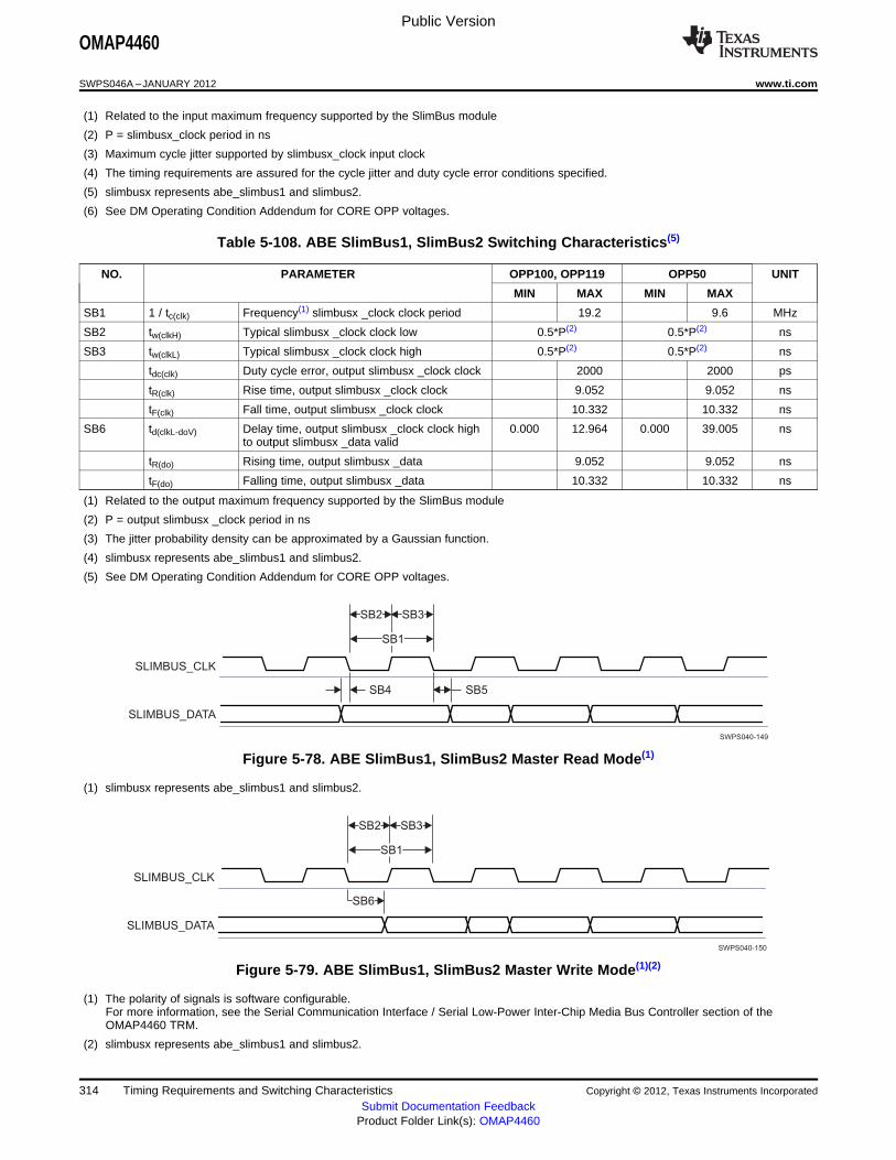
SWPS040-149
SLIMBUS_CLK
SLIMBUS_DATA
SB2 SB3
SB1
SB4 SB5
SWPS040-150
SLIMBUS_CLK
SLIMBUS_DATA
SB2 SB3
SB1
SB6
Public Version
OMAP4460
SWPS046A –JANUARY 2012 www.ti.com
(1) Related to the input maximum frequency supported by the SlimBus module
(2) P = slimbusx_clock period in ns
(3) Maximum cycle jitter supported by slimbusx_clock input clock
(4) The timing requirements are assured for the cycle jitter and duty cycle error conditions specified.
(5) slimbusx represents abe_slimbus1 and slimbus2.
(6) See DM Operating Condition Addendum for CORE OPP voltages.
Table 5-108. ABE SlimBus1, SlimBus2 Switching Characteristics(5)
NO. PARAMETER OPP100, OPP119 OPP50 UNIT
MIN MAX MIN MAX
SB1 1 / tc(clk) Frequency(1) slimbusx _clock clock period 19.2 9.6 MHz
SB2 tw(clkH) Typical slimbusx _clock clock low 0.5*P(2) 0.5*P(2) ns
SB3 tw(clkL) Typical slimbusx _clock clock high 0.5*P(2) 0.5*P(2) ns
tdc(clk) Duty cycle error, output slimbusx _clock clock 2000 2000 ps
tR(clk) Rise time, output slimbusx _clock clock 9.052 9.052 ns
tF(clk) Fall time, output slimbusx _clock clock 10.332 10.332 ns
SB6 td(clkL-doV) Delay time, output slimbusx _clock clock high 0.000 12.964 0.000 39.005 nsto output slimbusx _data valid
tR(do) Rising time, output slimbusx _data 9.052 9.052 ns
tF(do) Falling time, output slimbusx _data 10.332 10.332 ns
(1) Related to the output maximum frequency supported by the SlimBus module
(2) P = output slimbusx _clock period in ns
(3) The jitter probability density can be approximated by a Gaussian function.
(4) slimbusx represents abe_slimbus1 and slimbus2.
(5) See DM Operating Condition Addendum for CORE OPP voltages.
Figure 5-78. ABE SlimBus1, SlimBus2 Master Read Mode(1)
(1) slimbusx represents abe_slimbus1 and slimbus2.
Figure 5-79. ABE SlimBus1, SlimBus2 Master Write Mode(1)(2)
(1) The polarity of signals is software configurable.For more information, see the Serial Communication Interface / Serial Low-Power Inter-Chip Media Bus Controller section of theOMAP4460 TRM.
(2) slimbusx represents abe_slimbus1 and slimbus2.
314 Timing Requirements and Switching Characteristics Copyright © 2012, Texas Instruments Incorporated
Submit Documentation FeedbackProduct Folder Link(s): OMAP4460
Public Version
OMAP4460
www.ti.com SWPS046A –JANUARY 2012
5.6.7 High-Speed Synchronous Interface (HSI)
The MIPI high-speed synchronous serial interface (HSI) module is a multichannel and full duplex serialcommunications interface, composed of the HSI Transmitter (HSIT) in charge of the transmittedinformation and the HSI Receiver (HSIR) in charge of the received information. The HSI peripheral is usedtypically to enable OMAP to exchange information with an external modem. On the modem side, there isalso a receiver and a transmitter.
5.6.7.1 High-Speed Synchronous Interface 1
5.6.7.1.1 HSI1 Transmit and Receive Modes—1.2 V
Table 5-110 and Table 5-111 assume testing over the recommended operating conditions and electricalcharacteristic conditions below (see Figure 5-80 and Figure 5-81).
Table 5-109. HSI1 Timing Conditions—Transmit and Receive Modes—1.2 V(1)(2)(4)
SYSTEM CONDITION PARAMETER VALUE UNIT
MIN MAX
Input Conditions
tR Input signal rise time 1000 1300 ps
tF Input signal fall time 1000 1200 ps
PCB Conditions(3)
Number of external peripherals 1
Far end load 5 pF
Trace length 4 cm
Characteristics impedance 35 55 Ω
(1) IO settings: MB[1:0] = 11 and LB0 = 1, mode 3.For more information, see Control Module / Control Module Functional Description/ Functional Register Description / Signal IntegrityParameter Control Registers with Pad Group Assignment / I/Os with Combined Mode and Load Settings section of the OMAP4460TRM.
(2) In this table the rise and fall times are calculated for 20% to 80% of VDDS. For more information on the corresponding OMAP4 VDDSpower supply name, see Table 2-1, POWER [9] column with the ball name.
(3) Minimize the number of vias by layer transitions.
(4) To have an idea of the output OMAP4 ball load supported for this application, you can consider the following:Output OMAP4 ball load = Far End load + 1.34 pF/cm typical x trace length (cm).Output load CLOAD or Far end load equals to the total capacitance seen at the Far end of the transmission line.
Table 5-110. HSI1 Timing Requirements—Receive Mode—1.2 V(1)
NO. PARAMETER OPP100, OPP119 OPP50 UNIT
MIN MAX MIN MAX
1 / tc(data,flag) Frequency, hsi_cadata, hsi_caflag 112 56 MHz
HSI1 1 / tc(NomBit) Frequency, nominal bit time 225 112 MHz
HSI2 td(DAT-FLAG) Delay time, hsi_cadata transition to hsi_caflag 1.56 3.13 nstransition
td(FLAG-DAT) Delay time, hsi_caflag transition to hsi_cadata 1.56 3.13 nstransition
HSI3 td(DAT) Duration time, hsi_cadata low level or high 2.56 5.13 nslevel duration
td(FLAG) Duration time, hsi_caflag low level or high 2.56 5.13 nslevel duration
HSI4 tR Rise time, hsi_cadata and hsi_caflag 1.0 1.30 1.0 1.30 ns
HSI5 tF Fall time, hsi_cadata and hsi_caflag 1.0 1.20 1.0 1.20 ns
Copyright © 2012, Texas Instruments Incorporated Timing Requirements and Switching Characteristics 315Submit Documentation Feedback
Product Folder Link(s): OMAP4460
Public Version
OMAP4460
SWPS046A –JANUARY 2012 www.ti.com
(1) See DM Operating Condition Addendum for CORE OPP voltages.
Table 5-111. HSI1 Switching Characteristics—Transmit Mode—1.2 V(1)(2)(3)
NO. PARAMETER OPP100, OPP119 OPP50 UNIT
MIN MAX MIN MAX
1 / tc(data,flag) Frequency, hsi_acdata, hsi_acflag 96 48 MHz
HSI1 1 / tc(NomBit) Frequency, nominal bit time 192 96 MHz
HSI6 td(DAT-FLAG) Delay time, hsi_acdata transition to his_acflag 2.08 P + 0.98 4.17 P + 2.21 nstransition
td(FLAG-DAT) Delay time, hsi_acflag transition to hsi_acdata 2.08 P + 0.98 4.17 P + 2.21 nstransition
HSI7 td(DAT) Duration time, hsi_acdata low level or high 2.32 P + 1.18 4.42 P + 2.41 nslevel duration
td(FLAG) Duration time, hsi_acflag low level or high 2.32 P + 1.18 4.42 P + 2.41 nslevel duration
HSI8 tR Rise time, hsi_acdata and hsi_acflag 0.20 1.60 0.40 1.60 ns
HSI9 tF Fall time, hsi_acdata and hsi_acflag 0.20 1.40 0.30 1.40 ns
(1) Considered capacitive load is equal to 5 pF.
(2) P = tc(NomBit) time in ns
(3) See DM Operating Condition Addendum for CORE OPP voltages.
5.6.7.1.2 HSI1 Transmit and Receive Modes—1.8 V
Table 5-113 and Table 5-114 assume testing over the recommended operating conditions and electricalcharacteristic conditions below (see Figure 5-80 and Figure 5-81).
Table 5-112. HSI1 Timing Conditions—Transmit and Receive Modes—1.8 V(1)(2)(4)
SYSTEM CONDITION PARAMETER VALUE UNIT
MIN MAX
Input Conditions
tR Input signal rise time 1000 1500 ps
tF Input signal fall time 1000 1300 ps
PCB Conditions(3)
Number of external peripherals 1
Far end load 5 pF
Trace length 4 cm
Characteristics impedance 35 55 Ω
(1) IO settings: MB[1:0] = 11 and LB0 = 0, mode 3.For more information, see Control Module / Control Module Functional Description/ Functional Register Description / Signal IntegrityParameter Control Registers with Pad Group Assignment / I/Os with Combined Mode and Load Settings section of the OMAP4460TRM.
(2) In this table the rise and fall times are calculated for 20% to 80% of VDDS. For more information on the corresponding OMAP4 VDDSpower supply name, see Table 2-1, POWER [9] column with the ball name.
(3) Minimize the number of vias by layer transitions.
(4) To have an idea of the output OMAP4 ball load supported for this application, you can consider the following:Output OMAP4 ball load = Far End load + 1.34 pF/cm typical x trace length (cm).Output load CLOAD or Far end load equals to the total capacitance seen at the Far end of the transmission line.
Table 5-113. HSI1 Timing Requirements—Receive Mode—1.8 V(1)
NO. PARAMETER OPP100, OPP119 OPP50 UNIT
MIN MAX MIN MAX
1 / tc(data,flag) Frequency, hsi_cadata, hsi_caflag 112 56 MHz
HSI1 1 / tc(NomBit) Frequency, nominal bit time 225 112 MHz
316 Timing Requirements and Switching Characteristics Copyright © 2012, Texas Instruments Incorporated
Submit Documentation FeedbackProduct Folder Link(s): OMAP4460
Public Version
OMAP4460
www.ti.com SWPS046A –JANUARY 2012
Table 5-113. HSI1 Timing Requirements—Receive Mode—1.8 V(1) (continued)
NO. PARAMETER OPP100, OPP119 OPP50 UNIT
MIN MAX MIN MAX
HSI2 td(DAT-FLAG) Delay time, hsi_cadata transition to hsi_caflag 1.56 3.13 nstransition
td(FLAG-DAT) Delay time, hsi_caflag transition to hsi_cadata 1.56 3.13 nstransition
HSI3 td(DAT) Duration time, hsi_cadata low level or high level 2.56 5.13 nsduration
td(FLAG) Duration time, hsi_caflag low level or high level 2.56 5.13 nsduration
HSI4 tR Rise time, hsi_cadata and hsi_caflag 1.0 1.5 1.0 1.5 ns
HSI5 tF Fall time, hsi_cadata and hsi_caflag 1.0 1.3 1.0 1.3 ns
(1) See DM Operating Condition Addendum for CORE OPP voltages.
Table 5-114. HSI1 Switching Characteristics—Transmit Mode—1.8 V(1)(2)(3)
NO. PARAMETER OPP100, OPP119 OPP50 UNIT
MIN MAX MIN MAX
1 / tc(data,flag) Frequency, hsi_acdata, hsi_acflag 96 48 MHz
HSI1 1 / tc(NomBit) Frequency, nominal bit time 192 96 MHz
HSI6 td(DAT-FLAG) Delay time, hsi_acdata transition to his_acflag 2.08 P + 0.78 4.17 P + 1.91 nstransition
td(FLAG-DAT) Delay time, hsi_acflag transition to hsi_acdata 2.08 P + 0.78 4.17 P + 1.91 nstransition
HSI7 td(DAT) Duration time, hsi_acdata low level or high level 2.57 P + 1.18 4.69 P + 2.41 nsduration
td(FLAG) Duration time, hsi_acflag low level or high level 2.57 P + 1.18 4.69 P + 2.41 nsduration
HSI8 tR Rise time, hsi_acdata and hsi_acflag 0.40 1.70 0.60 1.70 ns
HSI9 tF Fall time, hsi_acdata and hsi_acflag 0.50 1.50 0.60 1.50 ns
(1) Considered capacitive load is equal to 5 pF.
(2) P = tc(NomBit) time in ns
(3) See DM Operating Condition Addendum for CORE OPP voltages.
5.6.7.2 High-Speed Synchronous Interface 2
5.6.7.2.1 HSI2 Transmit and Receive Modes—1.2 V
Table 5-116 and Table 5-117 assume testing over the recommended operating conditions and electricalcharacteristic conditions below (see Figure 5-80 and Figure 5-81).
Table 5-115. HSI2 Timing Conditions—Transmit and Receive Modes—1.2 V(1)(2)(4)
SYSTEM CONDITION PARAMETER VALUE UNIT
MIN MAX
Input Conditions
tR Input signal rise time 1000 1100 ps
tF Input signal fall time 1000 1100 ps
PCB Conditions(3)
Number of external peripherals 1
Far end load 5 pF
Trace length 4 cm
Characteristics impedance 35 50 Ω
Copyright © 2012, Texas Instruments Incorporated Timing Requirements and Switching Characteristics 317Submit Documentation Feedback
Product Folder Link(s): OMAP4460
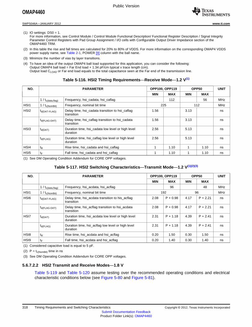
Public Version
OMAP4460
SWPS046A –JANUARY 2012 www.ti.com
(1) IO settings: DS0 = 1.For more information, see Control Module / Control Module Functional Description/ Functional Register Description / Signal IntegrityParameter Control Registers with Pad Group Assignment / I/O cells with Configurable Output Driver Impedance section of theOMAP4460 TRM.
(2) In this table the rise and fall times are calculated for 20% to 80% of VDDS. For more information on the corresponding OMAP4 VDDSpower supply name, see Table 2-1, POWER [9] column with the ball name.
(3) Minimize the number of vias by layer transitions.
(4) To have an idea of the output OMAP4 ball load supported for this application, you can consider the following:Output OMAP4 ball load = Far End load + 1.34 pF/cm typical x trace length (cm).Output load CLOAD or Far end load equals to the total capacitance seen at the Far end of the transmission line.
Table 5-116. HSI2 Timing Requirements—Receive Mode—1.2 V(1)
NO. PARAMETER OPP100, OPP119 OPP50 UNIT
MIN MAX MIN MAX
1 / tc(data,flag) Frequency, hsi_cadata, hsi_caflag 112 56 MHz
HSI1 1 / tc(NomBit) Frequency, nominal bit time 225 112 MHz
HSI2 td(DAT-FLAG) Delay time, hsi_cadata transition to hsi_caflag 1.56 3.13 nstransition
td(FLAG-DAT) Delay time, hsi_caflag transition to hsi_cadata 1.56 3.13 nstransition
HSI3 td(DAT) Duration time, hsi_cadata low level or high level 2.56 5.13 nsduration
td(FLAG) Duration time, hsi_caflag low level or high level 2.56 5.13 nsduration
HSI4 tR Rise time, hsi_cadata and hsi_caflag 1 1.10 1 1.10 ns
HSI5 tF Fall time, hsi_cadata and hsi_caflag 1 1.10 1 1.10 ns
(1) See DM Operating Condition Addendum for CORE OPP voltages.
Table 5-117. HSI2 Switching Characteristics—Transmit Mode—1.2 V(1)(2)(3)
NO. PARAMETER OPP100, OPP119 OPP50 UNIT
MIN MAX MIN MAX
1 / tc(data,flag) Frequency, hsi_acdata, hsi_acflag 96 48 MHz
HSI1 1 / tc(NomBit) Frequency, nominal bit time 192 96 MHz
HSI6 td(DAT-FLAG) Delay time, hsi_acdata transition to his_acflag 2.08 P + 0.98 4.17 P + 2.21 nstransition
td(FLAG-DAT) Delay time, hsi_acflag transition to hsi_acdata 2.08 P + 0.98 4.17 P + 2.21 nstransition
HSI7 td(DAT) Duration time, hsi_acdata low level or high level 2.31 P + 1.18 4.39 P + 2.41 nsduration
td(FLAG) Duration time, hsi_acflag low level or high level 2.31 P + 1.18 4.39 P + 2.41 nsduration
HSI8 tR Rise time, hsi_acdata and hsi_acflag 0.20 1.50 0.30 1.50 ns
HSI9 tF Fall time, hsi_acdata and hsi_acflag 0.20 1.40 0.30 1.40 ns
(1) Considered capacitive load is equal to 5 pF.
(2) P = tc(NomBit) time in ns
(3) See DM Operating Condition Addendum for CORE OPP voltages.
5.6.7.2.2 HSI2 Transmit and Receive Modes—1.8 V
Table 5-119 and Table 5-120 assume testing over the recommended operating conditions and electricalcharacteristic conditions below (see Figure 5-80 and Figure 5-81).
318 Timing Requirements and Switching Characteristics Copyright © 2012, Texas Instruments Incorporated
Submit Documentation FeedbackProduct Folder Link(s): OMAP4460

Public Version
OMAP4460
www.ti.com SWPS046A –JANUARY 2012
Table 5-118. HSI2 Timing Conditions—Transmit and Receive Modes—1.8 V(1)(2)(4)
SYSTEM CONDITION PARAMETER VALUE UNIT
MIN MAX
Input Conditions
tR Input signal rise time 1000 1300 ps
tF Input signal fall time 1000 1200 ps
PCB Conditions(3)
Number of external peripherals 1
Far end load 5 pF
Trace length 4 cm
Characteristics impedance 35 50 Ω
(1) IO settings: DS0 = 1.For more information, see Control Module / Control Module Functional Description/ Functional Register Description / Signal IntegrityParameter Control Registers with Pad Group Assignment / I/O cells with Configurable Output Driver Impedance section of theOMAP4460 TRM.
(2) In this table the rise and fall times are calculated for 20% to 80% of VDDS. For more information on the corresponding OMAP4 VDDSpower supply name, see Table 2-1, POWER [9] column with the ball name.
(3) Minimize the number of vias by layer transitions.The use of 15-Ω external serial resistance is recommended for transmit mode on hsi2_acdata (HSI2 APE to cellular modem data signal)and hsi2_acflag (HSI2 APE to cellular modem flag signal).In case the application needs both transmit and receive modes, the serial resistance is also recommended for receive mode onhsi2_cadata (HSI2 cellular modem to APE data signal) and hsi2_caflag (HSI2 cellular modem to APE flag signal).
(4) To have an idea of the output OMAP4 ball load supported for this application, you can consider the following:Output OMAP4 ball load = Far End load + 1.34 pF/cm typical x trace length (cm).Output load CLOAD or Far end load equals to the total capacitance seen at the Far end of the transmission line.
Table 5-119. HSI2 Timing Requirements—Receive Mode—1.8 V(1)
NO. PARAMETER OPP100, OPP119 OPP50 UNIT
MIN MAX MIN MAX
1 / tc(data,flag) Frequency, hsi_cadata, hsi_caflag 112 56 MHz
HSI1 1 / tc(NomBit) Frequency, nominal bit time 225 112 MHz
HSI2 td(DAT-FLAG) Delay time, hsi_cadata transition to hsi_caflag transition 1.56 3.13 ns
td(FLAG-DAT) Delay time, hsi_caflag transition to hsi_cadata transition 1.56 3.13 ns
HSI3 td(DAT) Duration time, hsi_cadata low level or high level duration 2.56 5.13 ns
td(FLAG) Duration time, hsi_caflag low level or high level duration 2.56 5.13 ns
HSI4 tR Rise time, hsi_cadata and hsi_caflag 1.0 1.30 1.0 1.30 ns
HSI5 tF Fall time, hsi_cadata and hsi_caflag 1.0 1.20 1.0 1.20 ns
(1) See DM Operating Condition Addendum for CORE OPP voltages.
Table 5-120. HSI2 Switching Characteristics—Transmit Mode—1.8 V(1)(2)(3)
NO. PARAMETER OPP100, OPP119 OPP50 UNIT
MIN MAX MIN MAX
1 / tc(data,flag) Frequency, hsi_acdata, hsi_acflag 96 48 MHz
HSI1 1 / tc(NomBit) Frequency, nominal bit time 192 96 MHz
HSI6 td(DAT-FLAG) Delay time, hsi_acdata transition to his_acflag transition 2.08 P + 0.98 4.17 P + 2.21 ns
td(FLAG-DAT) Delay time, hsi_acflag transition to hsi_acdata transition 2.08 P + 0.98 4.17 P + 2.21 ns
HSI7 td(DAT) Duration time, hsi_acdata low level or high level duration 2.35 P + 1.18 4.43 P + 2.41 ns
td(FLAG) Duration time, hsi_acflag low level or high level duration 2.35 P + 1.18 4.43 P + 2.41 ns
HSI8 tR Rise time, hsi_acdata and hsi_acflag 0.20 1.60 0.30 1.60 ns
HSI9 tF Fall time, hsi_acdata and hsi_acflag 0.20 1.40 0.30 1.40 ns
Copyright © 2012, Texas Instruments Incorporated Timing Requirements and Switching Characteristics 319Submit Documentation Feedback
Product Folder Link(s): OMAP4460
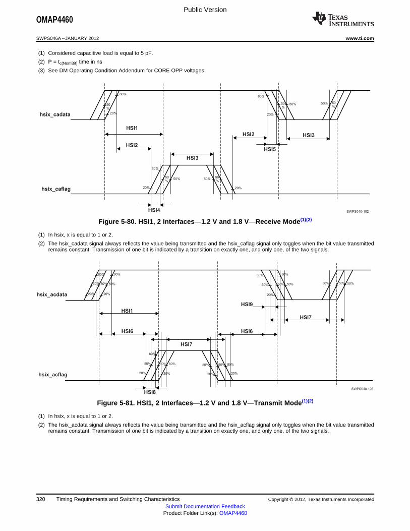
HSI1
HSI3
HSI4
hsix_caflag
HSI2
hsix_cadata
HSI2
HSI3
50% 50%
HSI5
50%50%
20%
80%
20%
80%
20%
80%
20%
50
%
50
%
50
%
50
%
SWPS040-102
50
%
hsix_acflag
hsix_acdata
HSI1
HSI9
HSI7
HSI8
HSI6 HSI6
HSI7
50% 50%50% 50% 50%50%
50% 50%50%50% 50%50% 50% 50%50%
20%
80%
20%
80%
20%20%
20%
20%20%
80% 80%
80%
SWPS040-103
Public Version
OMAP4460
SWPS046A –JANUARY 2012 www.ti.com
(1) Considered capacitive load is equal to 5 pF.
(2) P = tc(NomBit) time in ns
(3) See DM Operating Condition Addendum for CORE OPP voltages.
Figure 5-80. HSI1, 2 Interfaces—1.2 V and 1.8 V—Receive Mode(1)(2)
(1) In hsix, x is equal to 1 or 2.
(2) The hsix_cadata signal always reflects the value being transmitted and the hsix_caflag signal only toggles when the bit value transmittedremains constant. Transmission of one bit is indicated by a transition on exactly one, and only one, of the two signals.
Figure 5-81. HSI1, 2 Interfaces—1.2 V and 1.8 V—Transmit Mode(1)(2)
(1) In hsix, x is equal to 1 or 2.
(2) The hsix_acdata signal always reflects the value being transmitted and the hsix_acflag signal only toggles when the bit value transmittedremains constant. Transmission of one bit is indicated by a transition on exactly one, and only one, of the two signals.
320 Timing Requirements and Switching Characteristics Copyright © 2012, Texas Instruments Incorporated
Submit Documentation FeedbackProduct Folder Link(s): OMAP4460

Public Version
OMAP4460
www.ti.com SWPS046A –JANUARY 2012
5.6.8 Universal Serial Bus (USB)
5.6.8.1 Universal Serial Bus (USB)—USBA0
NOTEFor more information, see the Serial Communication Interface / High-Speed USB OTGController section of the OMAP4460 TRM.
5.6.8.1.1 High-Speed USBA0 (HSUSB)—USB HS OTG PHY
The USB HS OTG PHY module fits the High-speed Signaling Eye Patterns and Rise and Fall Time of theUSB specification Revision 2.0, provided the PCB guidelines are followed (for more information on thePCB guidelines, see Section A, OMAP4460 Processor Multimedia Device PCB Guideline). For moreinformation on the High-speed Signaling Eye Patterns and Rise and Fall Time, see the Electrical /Signaling / Data Signal Rise and Fall, Eye Patterns / High-speed Signaling Eye Patterns and Rise and FallTime section of the USB specification Revision 2.0:• For USB HS transmit waveform requirements, see Figure 7-13 (Template 1).• For USB HS receiver sensitivity waveform requirements, see Figure 7-16 (Template 4).
5.6.8.1.2 High-Speed USBA0 (HSUSB)—ULPI SDR—Slave Mode
Table 5-122 and Table 5-123 assume testing over the recommended operating conditions and electricalcharacteristic conditions below (see Figure 5-82).
Table 5-121. High-Speed USB USBA0 Timing Conditions—ULPI SDR—Slave Mode—1.8 V(1)(2)(3)
SYSTEM CONDITION PARAMETER VALUE UNIT
MIN MAX
Input Conditions
tR Input signal rise time 1.00 3.00 ns
tF Input signal fall time 1.00 3.00 ns
PCB Conditions
Number of external peripherals 1
Far end load 5 pF
Trace length 5 cm
Characteristics impedance 30 60 Ω
(1) IO settings configuration: DS0 = 0Corresponding voltage: 1.8 VFor more information, see Control Module / Control Module Functional Description/ Functional Register Description / Signal IntegrityParameter Control Registers with Pad Group Assignment / I/O cells with Configurable Output Driver Impedance section of theOMAP4460 TRM.
(2) In this table the rise and fall times are calculated for 20% to 80% of VDDS. For more information on the corresponding OMAP4 VDDSpower supply name, see Table 2-1, POWER [9] column with the ball name.
(3) To have an idea of the output OMAP4 ball load supported for this application, you can consider the following:Output OMAP4 ball load = Far End load + 1.34 pF/cm typical x trace length (cm).
Table 5-122. High-Speed USB USBA0 Timing Requirements—ULPI SDR—Slave Mode—1.8 V(4)
NO. PARAMETER OPP100, OPP119 UNIT
MIN MAX
US1 1 / tc(clk) Frequency(1), usba0_ulpiphy_clk 60 MHz
US2 tw(clkH) Typical pulse duration, usba0_ulpiphy_clk high 0.5*P(2) ns
US3 tw(clkL) Typical pulse duration, usba0_ulpiphy_clk low 0.5*P(2) ns
tdc(clk) Duty cycle error, usba0_ulpiphy_clk –833 833 ps
tj(clk) Jitter standard deviation(3), usba0_ulpiphy_clk 500 ps
Copyright © 2012, Texas Instruments Incorporated Timing Requirements and Switching Characteristics 321Submit Documentation Feedback
Product Folder Link(s): OMAP4460
usba0_ulpiphy_clk
usba0_ulpiphy_stp
usba0_ulpiphy_dir_&_nxt
usba0_ulpiphy_dat[7:0]
US1
US8US9
US9
US2
US4 US4
US5US6
DATA_IN DATA_OUT
US3
US7
SWPS040-128
Public Version
OMAP4460
SWPS046A –JANUARY 2012 www.ti.com
Table 5-122. High-Speed USB USBA0 Timing Requirements—ULPI SDR—Slave Mode—1.8V(4) (continued)
NO. PARAMETER OPP100, OPP119 UNIT
MIN MAX
US5 tsu(ctrlV-clkH) Setup time, usba0_ulpiphy_dir and usba0_ulpiphy_nxt valid before 6.73 nsusba0_ulpiphy_clk rising edge
US6 th(clkH-ctrlV) Hold time, usba0_ulpiphy_dir and usba0_ulpiphy_nxt valid after 0.00 nsusba0_ulpiphy_clk rising edge
US7 tsu(dV-clkH) Setup time, input usba0_ulpiphy_dat[7:0] valid before 6.73 nsusba0_ulpiphy_clk rising edge
US8 th(clkH-dV) Hold time, input usba0_ulpiphy_dat[7:0] valid after usba0_ulpiphy_clk 0.00 nsrising edge
(1) Related to the input maximum frequency supported by the USB module.
(2) P = clk period in ns
(3) Maximum cycle jitter supported by clock input clock.
(4) See DM Operating Condition Addendum for CORE OPP voltages.
Table 5-123. High-Speed HSUSB USBA0 Switching Characteristics—ULPI SDR—Slave Mode—1.8 V(1)
NO. PARAMETER OPP100, OPP119 UNIT
MIN MAX
US4 td(clkL-ctrlV) Delay time, usba0_ulpiphy_clk rising edge high to output 0.40 8.34 nsusba0_ulpiphy_stp valid
tR(ctrl) Rise time, output usba0_ulpiphy_stp 3.0 ps
tF(dtrl) Fall time, output usba0_ulpiphy_stp 3.0 ps
US9 td(clkL-doV) Delay time, usba0_ulpiphy_clk rising edge to output 0.40 8.34 nsusba0_ulpiphy_dat[7:0] valid
tR(do) Rise time, output usba0_ulpiphy_dat[7:0] 3.0 ps
tF(do) Fall time, output usba0_ulpiphy_dat[7:0] 3.0 ps
(1) See DM Operating Condition Addendum for CORE OPP voltages.
Figure 5-82. High-Speed USB USBA0—ULPI SDR—Slave Mode—1.8 V
5.6.8.2 Universal Serial Bus (USB)—USBC1
NOTEFor more information, see the Serial Communication Interface / Full-Speed USB HostController section of the OMAP4460 TRM.
322 Timing Requirements and Switching Characteristics Copyright © 2012, Texas Instruments Incorporated
Submit Documentation FeedbackProduct Folder Link(s): OMAP4460

Public Version
OMAP4460
www.ti.com SWPS046A –JANUARY 2012
5.6.8.2.1 Low- / Full-Speed USBC1 (FSUSB)—Bidirectional Standard 4-pin Mode
Table 5-125 and Table 5-126 assume testing over the recommended operating conditions and electricalcharacteristic conditions below (see Figure 5-83).
Table 5-124. Low- / Full-Speed USBC1 Timing Conditions—Bidirectional Standard 4-pin Mode—1.8 V(1)(2)(3)
TIMING CONDITION PARAMETER VALUE UNIT
MIN MAX
Input Conditions
tR Input signal rise time 2 ns
tF Input signal fall time 2 ns
PCB Conditions
Number of external peripherals 1
Far end load 10 pF
Trace length 10 cm
Characteristics impedance 30 60 Ω
(1) IO settings:
– usbc1_icusb_txen (ball D23): LB0 = 0For more information, see the Control Module / Control Module Functional Description/ Functional Register Description / SignalIntegrity Parameter Control Registers with Pad Group Assignment section of the OMAP4460 TRM.
– usbc1_icusb_dp, usbc1_icusb_dm, usbc1_icusb_txen, usbc1_icusb_rcv (balls AE5, AF5, AF4, AE4): MB[1:0] = 10, LB0 = 1For more information, see Control Module / Control Module Functional Description/ Functional Register Description / Signal IntegrityParameter Control Registers with Pad Group Assignment / 50-Ω Output Buffer I/Os with Combined Mode and Load Settings sectionof the OMAP4460 TRM.
– Corresponding voltage: 1.8 V
(2) In this table the rise and fall times are calculated for 10% to 90% of VDDS. For more information on the corresponding OMAP4 VDDSpower supply name, see Table 2-1, POWER [9] column with the ball name.
(3) To have an idea of the output OMAP4 ball load supported for this application, you can consider the following:Output OMAP4 ball load = Far End load + 1.34 pF/cm typical x trace length (cm).
Copyright © 2012, Texas Instruments Incorporated Timing Requirements and Switching Characteristics 323Submit Documentation Feedback
Product Folder Link(s): OMAP4460

usbc1_icusb_txen
usbc1_icusb_dp (TXDAT)
usbc1_icusb_dm (TSE0)
usbc1_icusb_rcv
Transmit Receive
FSU14
FSU15 FSU16
FSU17
FSU18
FSU10
FSU10
FSU13FSU12
FSU11
FSU11
SWPS040-129
Public Version
OMAP4460
SWPS046A –JANUARY 2012 www.ti.com
Table 5-125. Low- / Full-Speed USBC1 Timing Requirements—Bidirectional Standard 4-pin Mode—1.8V(1)(2)
NO. PARAMETER OPP100, OPP119 OPP50 UNIT
MIN MAX MIN MAX
FSU10 td(DAT,SE0) Time duration, usbc1_icusb_dp (TXDAT, ball AE5) 14.0 14.0 nsand usbc1_icusb_dm (TSE0, ball AF5) low togetherduring transition
FSU11 td(DAT,SE0) Time duration, usbc1_icusb_dp (TXDAT, ball AE5) 8.0 8.0 nsand usbc1_icusb_dm (TSE0, ball AF5) high togetherduring transition
FSU12 td(RCVU0) Time duration, usbc1_icusb_rcv undefined during a 14.0 14.0 nsSingle End 0 (usbc1_icusb_dp (TXDAT, ball AE5) andusbc1_icusb_dm (TSE0, ball AF5) low together)
FSU13 td(RCVU1) Time duration, usbc1_icusb_rcv undefined during a 8.0 8.0 nsSingle End 1 (usbc1_icusb_dp (TXDAT, ball AE5) andusbc1_icusb_dm (TSE0, ball AF5) high together)
(1) See DM Operating Condition Addendum for CORE OPP voltages.
(2) Low-Speed mode is a subset of the Full-Speed mode and it is expected to work at low bandwidth (1.5Mb/s).
Table 5-126. Low- / Full-Speed USBC1 Switching Characteristics—Bidirectional Standard 4-pin Mode—1.8V(1)(2)
NO. PARAMETER OPP100, OPP119 OPP50 UNIT
MIN MAX MIN MAX
FSU14 td(TXENL-DATV) Delay time usbc1_icusb_txen low to 81.8 84.8 81.8 84.8 nsusbc1_icusb_dp (TXDAT, ball AE5) valid
FSU15 td(TXENL-SE0V) Delay time usbc1_icusb_txen low to 81.8 84.8 81.8 84.8 nsusbc1_icusb_dm (TSE0, ball AF5) valid
FSU16 tsk(DAT-SE0) Skew between usbc1_icusb_dp (TXDAT, ball 1.5 1.5 nsAE5) and usbc1_icusb_dm (TSE0, ball AF5)transition
FSU17 td(DATV-TXENH) Delay time, usbc1_icusb_dp (TXDAT, ball 81.8 81.8 nsAE5) invalid before usbc1_icusb_txen high
FSU18 td(SE0V-TXENH) Delay time, usbc1_icusb_dm (TSE0, ball AF5) 81.8 81.8 nsinvalid before usbc1_icusb_txen high
(1) See DM Operating Condition Addendum for CORE OPP voltages.
(2) Low-Speed mode is a subset of the Full-Speed mode and it is expected to work at low bandwidth (1.5Mb/s).
Figure 5-83. Low- / Full-Speed USBC1—Bidirectional Standard 4-pin Mode—1.8 V(1)
(1) To have usbc1_icusb_dm as TXDAT signal, use ball AF5.To have usbc1_icusb_dp as TXSE0 signal, use ball AE5.
5.6.8.2.2 Low- / Full-Speed USBC1 (FSUSB)—Bidirectional Standard 4-pin TLL Mode
Table 5-128 and Table 5-129 assume testing over the recommended operating conditions and electricalcharacteristic conditions below (see Figure 5-84).
324 Timing Requirements and Switching Characteristics Copyright © 2012, Texas Instruments Incorporated
Submit Documentation FeedbackProduct Folder Link(s): OMAP4460

Public Version
OMAP4460
www.ti.com SWPS046A –JANUARY 2012
Table 5-127. Low- / Full-Speed USBC1 Timing Conditions—Bidirectional Standard 4-pin TLL Mode—1.8V(1)(2)(3)
TIMING CONDITION PARAMETER VALUE UNIT
MIN MAX
Input Conditions
tR Input signal rise time 2 ns
tF Input signal fall time 2 ns
PCB Conditions
Number of external peripherals 1
Far end load 10 pF
Trace length 10 cm
Characteristics impedance 30 60 Ω
(1) IO settings:
– usbc1_icusb_txen (ball D23): LB0 = 0For more information, see the Control Module / Control Module Functional Description/ Functional Register Description / SignalIntegrity Parameter Control Registers with Pad Group Assignment section of the OMAP4460 TRM.
– usbc1_icusb_dp, usbc1_icusb_dm, usbc1_icusb_txen, usbc1_icusb_rcv (balls AE5, AF5, AF4, AE4): MB[1:0] = 10, LB0 = 1For more information, see Control Module / Control Module Functional Description/ Functional Register Description / Signal IntegrityParameter Control Registers with Pad Group Assignment / 50-Ω Output Buffer I/Os with Combined Mode and Load Settings sectionof the OMAP4460 TRM.
– Corresponding voltage: 1.8 V
(2) In this table the rise and fall times are calculated for 10% to 90% of VDDS. For more information on the corresponding OMAP4 VDDSpower supply name, see Table 2-1, POWER [9] column with the ball name.
(3) To have an idea of the output OMAP4 ball load supported for this application, you can consider the following:Output OMAP4 ball load = Far End load + 1.34 pF/cm typical x trace length (cm).
Table 5-128. Low- / Full-Speed USBC1 Timing Requirements—Bidirectional Standard 4-pin TLLMode—1.8 V(1)(2)
NO. PARAMETER OPP100, OPP119 OPP50 UNIT
MIN MAX MIN MAX
FSUT9 td(DAT,SE0) Time duration, usbc1_icusb_dp (TXDAT, ball 14.0 14.0 nsAE5) and usbc1_icusb_dm (TSE0, ball AF5)low together during transition
FSUT10 td(DAT,SE0) Time duration, usbc1_icusb_dp (TXDAT, ball 8.0 8.0 nsAE5) and usbc1_icusb_dm (TSE0, ball AF5)high together during transition
(1) See DM Operating Condition Addendum for CORE OPP voltages.
(2) Low-Speed mode is a subset of the Full-Speed mode and it is expected to work at low bandwidth (1.5Mb/s).
Table 5-129. Low- / Full-Speed USBC1 Switching Characteristics—Bidirectional Standard 4-pin TLLMode—1.8 V(1)(2)
NO. PARAMETER OPP100, OPP119 OPP50 UNIT
MIN MAX MIN MAX
FSUT11 td(TXENL-DATV) Delay time usbc1_icusb_txen active to 81.8 84.8 81.8 84.8 nsusbc1_icusb_dp (TXDAT, ball AE5) valid
FSUT12 td(TXENL-SE0V) Delay time usbc1_icusb_txen active to 81.8 84.8 81.8 84.8 nsusbc1_icusb_dm (TSE0, ball AF5) valid
FSUT13 tsk(DAT-SE0) Skew between usbc1_icusb_dp (TXDAT, ball 1.5 1.5 nsAE5) and usbc1_icusb_dm (TSE0, ball AF5)transition
FSUT14 tsk(DP,DM-RCV) Skew between usbc1_icusb_dp (TXDAT, ball 1.5 1.5 nsAE5), usbc1_icusb_dm (TSE0, ball AF5) andusbc1_icusb_rcv transition
FSUT15 td(DATI-TXENL) Delay time usbc1_icusb_dm (TSE0, ball AF5) 81.8 81.8 nsinvalid to usbc1_icusb_txen Low
Copyright © 2012, Texas Instruments Incorporated Timing Requirements and Switching Characteristics 325Submit Documentation Feedback
Product Folder Link(s): OMAP4460

usbc1_icusb_txen
usbc1_icusb_dp (TXDAT, ball AE5)
usbc1_icusb_dm (TSE0, ball AF5)
usbc1_icusb_rcv
Transmit Receive
FSUT11
FSUT12 FSUT13
FSUT15
FSUT16
FSUT9
FSUT9
FSUT10
FSUT10
SWPS040-130
FSUT14
Public Version
OMAP4460
SWPS046A –JANUARY 2012 www.ti.com
Table 5-129. Low- / Full-Speed USBC1 Switching Characteristics—Bidirectional Standard 4-pin TLLMode—1.8 V(1)(2) (continued)
NO. PARAMETER OPP100, OPP119 OPP50 UNIT
MIN MAX MIN MAX
FSUT16 td(SE0I-TXENL) Delay time usbc1_icusb_dp (TXDAT, ball AE5) 81.8 81.8 nsinvalid to usbc1_icusb_txen Low
(1) See DM Operating Condition Addendum for CORE OPP voltages.
(2) Low-Speed mode is a subset of the Full-Speed mode and it is expected to work at low bandwidth (1.5Mb/s).
Figure 5-84. Low- / Full-Speed USBC1—Bidirectional Standard 4-pin TLL Mode—1.8 V(1)
(1) To have usbc1_icusb_dm as TXDAT signal, use ball AF5.To have usbc1_icusb_dp as TXSE0 signal, use ball AE5.
5.6.8.2.3 Low- / Full-Speed USBC1 (FSUSB)—Bidirectional 2-pin Mode
Table 5-131 assumes testing over the recommended operating conditions and electrical characteristicconditions below (see Figure 5-85).
Table 5-130. Low- / Full-Speed USBC1 Timing Conditions—Bidirectional 2-pin Mode—1.8 V, 3.3 V(1)(2)(3)
TIMING CONDITION PARAMETER VALUE UNIT
MIN MAX
Input Conditions
tR Input signal rise time 2 ns
tF Input signal fall time 2 ns
PCB Conditions
Number of external peripherals 1
Far end load 10 pF
Trace length 10 cm
Characteristics impedance 30 60 Ω
(1) IO settings:
– usbc1_icusb_dp, usbc1_icusb_dm (balls H2, H3): SPEECTRL = 0For more information see, USBC1_DR0_SPEEDCTRL register in Control Module / Control Module Functional Description/Functional Register Description / Signal Integrity Parameter Control Registers with Pad Group Assignment / Device InterfacesSignal Group Controls Mapping section of OMAP4460 TRM.
– Corresponding voltages: 1.8 V, 3.3 V
(2) In this table the rise and fall times are calculated for 10% to 90% of VDDS. For more information on the corresponding OMAP4 VDDSpower supply name, see Table 2-1, POWER [9] column with the ball name.
(3) To have an idea of the output OMAP4 ball load supported for this application, you can consider the following:Output OMAP4 ball load = Far End load + 1.34 pF/cm typical x trace length (cm).
326 Timing Requirements and Switching Characteristics Copyright © 2012, Texas Instruments Incorporated
Submit Documentation FeedbackProduct Folder Link(s): OMAP4460

FSU2FSU1
SWPS040-131
usbc1_icusb_dm (Ball H3)
FSU2FSU1
usbc1_icusb_dp (Ball H2)
Public Version
OMAP4460
www.ti.com SWPS046A –JANUARY 2012
Table 5-131. Low- / Full-Speed USBC1 Timing Requirements—Bidirectional 2-pin Mode—1.8 V, 3.3 V(1)(2)
NO. PARAMETER OPP100, OPP119 OPP50 UNIT
MIN MAX MIN MAX
FSU1 td(DAT,SE0) Time duration, usbc1_icusb_dp (TXDAT, ball 14.0 14.0 nsH2) and usbc1_icusb_dm (TSE0, ball H3) lowtogether during transition
FSU2 td(DAT,SE0) Time duration, usbc1_icusb_dp (TXDAT, ball 8.0 8.0 nsH2) and usbc1_icusb_dm (TSE0, ball H3) hightogether during transition
(1) See DM Operating Condition Addendum for CORE OPP voltages.
(2) Low-Speed mode is a subset of the Full-Speed mode and it is expected to work at low bandwidth (1.5Mb/s).
Figure 5-85. Low- / Full-Speed USBC1—Bidirectional 2-pin Mode—1.8 V, 3.3 V(1)
(1) To use usbc1_icusb_dm as TXDAT signal, use ball H3.To use usbc1_icusb_dp as TXSE0 signal, use ball H2.
5.6.8.3 Universal Serial Bus (USB)—USBB1
NOTEFor more information, see the Serial Communication Interface / High-Speed Multiport USBHost Subsystem section of the OMAP4460 TRM.
5.6.8.3.1 Low- / Full-Speed USBB1 (FSUSB)—Bidirectional Standard 4-pin Mode
Table 5-133 and Table 5-134 assume testing over the recommended operating conditions and electricalcharacteristic conditions below (see Figure 5-86).
Table 5-132. Low- / Full-Speed USBB1 Timing Conditions—Bidirectional Standard 4-pin Mode—1.8 V(1)(2)(3)
TIMING CONDITION PARAMETER VALUE UNIT
MIN MAX
Input Conditions
tR Input signal rise time 2 ns
tF Input signal fall time 2 ns
PCB Conditions
Number of external peripherals 1
Far end load 10 pF
Trace length 10 cm
Characteristics impedance 30 60 Ω
(1) IO settings:
– usbb1_mm_txen (ball AF18): MB[1:0] = 10, LB0 = 1– usbb1_mm_txdat (ball AG18): MB[1:0] = 10, LB0 = 1– usbb1_mm_txse0 (ball AE17): MB[1:0] = 10, LB0 = 1– usbb1_mm_rxrcv (ball AF17): MB[1:0] = 10, LB0 = 1
For more information, see Control Module / Control Module Functional Description/ Functional Register Description / Signal IntegrityParameter Control Registers with Pad Group Assignment / Low Speed I/Os Combined Slew Rate vs TL Length and Load Settingssection of the OMAP4460 TRM.
– Corresponding voltage: 1.8 V
(2) In this table the rise and fall times are calculated for 10% to 90% of VDDS. For more information on the corresponding OMAP4 VDDSpower supply name, see Table 2-1, POWER [9] column with the ball name.
Copyright © 2012, Texas Instruments Incorporated Timing Requirements and Switching Characteristics 327Submit Documentation Feedback
Product Folder Link(s): OMAP4460

usbb1_mm_txen
usbb1_mm_txdat
usbb1_mm_txse0
usbb1_mm_rxrcv
Transmit Receive
FSU14
FSU15 FSU16
FSU17
FSU18
FSU10
FSU10
FSU13FSU12
FSU11
FSU11
SWPS040-132
Public Version
OMAP4460
SWPS046A –JANUARY 2012 www.ti.com
(3) To have an idea of the output OMAP4 ball load supported for this application, you can consider the following:Output OMAP4 ball load = Far End load + 1.34 pF/cm typical x trace length (cm).
Table 5-133. Low- / Full-Speed USBB1 Timing Requirements—Bidirectional Standard 4-pin Mode—1.8V(1)(2)
NO. PARAMETER OPP100, OPP119 OPP50 UNIT
MIN MAX MIN MAX
FSU10 td(DAT,SE0) Time duration, usbb1_mm_txdat and 14.0 14.0 nsusbb1_mm_txse0 low together duringtransition
FSU11 td(DAT,SE0) Time duration, usbb1_mm_txdat and 8.0 8.0 nsusbb1_mm_txse0 high together duringtransition
FSU12 td(RCVU0) Time duration, usbb1_mm_rxrcv undefined 14.0 14.0 nsduring a Single End 0 (usbb1_mm_txdat andusbb1_mm_txse0 low together)
FSU13 td(RCVU1) Time duration, usbb1_mm_rxrcv undefined 8.0 8.0 nsduring a Single End 1 (usbb1_mm_txdat andusbb1_mm_txse0 high together)
(1) See DM Operating Condition Addendum for CORE OPP voltages.
(2) Low-Speed mode is a subset of the Full-Speed mode and it is expected to work at low bandwidth (1.5Mb/s).
Table 5-134. Low- / Full-Speed USBB1 Switching Characteristics—Bidirectional Standard 4-pin Mode—1.8V(1)(2)
NO. PARAMETER OPP100, OPP119 OPP50 UNIT
MIN MAX MIN MAX
FSU14 td(TXENL-DATV) Delay time usbb1_mm_txen low to 81.8 84.8 81.8 84.8 nsusbb1_mm_txdat valid
FSU15 td(TXENL-SE0V) Delay time usbb1_mm_txen low to 81.8 84.8 81.8 84.8 nsusbb1_mm_txse0 valid
FSU16 tsk(DAT-SE0) Skew between usbb1_mm_txdat and 1.5 1.5 nsusbb1_mm_txse0 transition
FSU17 td(DATV-TXENH) Delay time, usbb1_mm_txdat invalid before 81.8 81.8 nsusbb1_mm_txen high
FSU18 td(SE0V-TXENH) Delay time, usbb1_mm_txse0 invalid before 81.8 81.8 nsusbb1_mm_txen high
(1) See DM Operating Condition Addendum for CORE OPP voltages.
(2) Low-Speed mode is a subset of the Full-Speed mode and it is expected to work at low bandwidth (1.5Mb/s).
Figure 5-86. Low- / Full-Speed USBB1—Bidirectional Standard 4-pin Mode—1.8 V
328 Timing Requirements and Switching Characteristics Copyright © 2012, Texas Instruments Incorporated
Submit Documentation FeedbackProduct Folder Link(s): OMAP4460

Public Version
OMAP4460
www.ti.com SWPS046A –JANUARY 2012
5.6.8.3.2 Low- / Full-Speed USBB1 (FSUSB)—Bidirectional Standard 4-pin TLL Mode
Table 5-136 and Table 5-137 assume testing over the recommended operating conditions and electricalcharacteristic conditions below (see Figure 5-87).
Table 5-135. Low- / Full-Speed USBB1 Timing Conditions—Bidirectional TLL 4-pin Mode—1.8 V(1)(2)(3)
TIMING CONDITION PARAMETER VALUE UNIT
MIN MAX
Input Conditions
tR Input signal rise time 2 ns
tF Input signal fall time 2 ns
PCB Conditions
Number of external peripherals 1
Far end load 10 pF
Trace length 10 cm
Characteristics impedance 30 60 Ω
(1) IO settings:
– usbb1_mm_txen (ball AF18): MB[1:0] = 10, LB0 = 1– usbb1_mm_txdat (ball AG18): MB[1:0] = 10, LB0 = 1– usbb1_mm_txse0 (ball AE17): MB[1:0] = 10, LB0 = 1– usbb1_mm_rxrcv (ball AF17): MB[1:0] = 10, LB0 = 1
For more information, see Control Module / Control Module Functional Description/ Functional Register Description / Signal IntegrityParameter Control Registers with Pad Group Assignment / Low Speed I/Os Combined Slew Rate vs TL Length and Load Settingssection of the OMAP4460 TRM.
– Corresponding voltage: 1.8 V
(2) In this table the rise and fall times are calculated for 10% to 90% of VDDS. For more information on the corresponding OMAP4 VDDSpower supply name, see Table 2-1, POWER [9] column with the ball name.
(3) To have an idea of the output OMAP4 ball load supported for this application, you can consider the following:Output OMAP4 ball load = Far End load + 1.34 pF/cm typical x trace length (cm).
Table 5-136. Low- / Full-Speed USBB1 Timing Requirements—Bidirectional TLL 4-pin Mode—1.8 V(1)(2)
NO. PARAMETER OPP100, OPP119 OPP50 UNIT
MIN MAX MIN MAX
FSU9 td(DAT,SE0) Time duration, usbb1_mm_txdat and 14.0 14.0 nsusbb1_mm_txse0 low together duringtransition
FSU10 td(DAT,SE0) Time duration, usbb1_mm_txdat and 8.0 8.0 nsusbb1_mm_txse0 high together duringtransition
(1) See DM Operating Condition Addendum for CORE OPP voltages.
(2) Low-Speed mode is a subset of the Full-Speed mode and it is expected to work at low bandwidth (1.5Mb/s).
Table 5-137. Low- / Full-Speed USBB1 Switching Characteristics—Bidirectional TLL 4-pin Mode—1.8V(1)(2)
NO. PARAMETER OPP100, OPP119 OPP50 UNIT
MIN MAX MIN MAX
FSU11 td(TXENL-DATV) Delay time usbb1_mm_txen low to 81.8 84.8 81.8 84.8 nsusbb1_mm_txdat valid
FSU12 td(TXENL-SE0V) Delay time usbb1_mm_txen low to 81.8 84.8 81.8 84.8 nsusbb1_mm_txse0 valid
FSU13 tsk(DAT-SE0) Skew between usbb1_mm_txdat and 1.5 1.5 nsusbb1_mm_txse0 transition
FSU14 tsk(DAT-SE0) Skew between usbb1_mm_txdat, usbb1_txse0 1.5 1.5 nsand usbb1_mm_rxrcv transition
Copyright © 2012, Texas Instruments Incorporated Timing Requirements and Switching Characteristics 329Submit Documentation Feedback
Product Folder Link(s): OMAP4460

usbb1_mm_txen
usbb1_mm_txdat
usbb1_mm_txse0
usbb1_mm_rxrcv
Transmit Receive
FSU11
FSU12 FSU13
FSU15
FSU16
FSU9
FSU9
FSU10
FSU10
SWPS040-133
FSU14
Public Version
OMAP4460
SWPS046A –JANUARY 2012 www.ti.com
Table 5-137. Low- / Full-Speed USBB1 Switching Characteristics—Bidirectional TLL 4-pin Mode—1.8V(1)(2) (continued)
NO. PARAMETER OPP100, OPP119 OPP50 UNIT
MIN MAX MIN MAX
FSU15 td(DATV-TXENH) Delay time, usbb1_mm_txdat invalid before 81.8 81.8 nsusbb1_mm_txen high
FSU16 td(SE0V-TXENH) Delay time, usbb1_mm_txse0 invalid before 81.8 81.8 nsusbb1_mm_txen high
(1) See DM Operating Condition Addendum for CORE OPP voltages.
(2) Low-Speed mode is a subset of the Full-Speed mode and it is expected to work at low bandwidth (1.5Mb/s).
Figure 5-87. Low- / Full-Speed USBB1—Bidirectional TLL 4-pin Mode—1.8 V
5.6.8.3.3 Low- / Full-Speed USBB1 (FSUSB)—Bidirectional Standard 3-pin Mode
Table 5-139 and Table 5-140 assume testing over the recommended operating conditions and electricalcharacteristic conditions below (see Figure 5-88).
Table 5-138. Low- / Full-Speed USBB1 Timing Conditions—Bidirectional Standard 3-pin Mode—1.8 V(1)(2)(3)
TIMING CONDITION PARAMETER VALUE UNIT
MIN MAX
Input Conditions
tR Input signal rise time 2 ns
tF Input signal fall time 2 ns
PCB Conditions
Number of external peripherals 1
Far end load 10 pF
Trace length 10 cm
Characteristics impedance 30 60 Ω
(1) IO settings:
– usbb1_mm_txen (ball AF18): MB[1:0] = 10, LB0 = 1– usbb1_mm_txdat (ball AG18): MB[1:0] = 10, LB0 = 1– usbb1_mm_txse0 (ball AE17): MB[1:0] = 10, LB0 = 1
For more information, see Control Module / Control Module Functional Description/ Functional Register Description / Signal IntegrityParameter Control Registers with Pad Group Assignment / Low Speed I/Os Combined Slew Rate vs TL Length and Load Settingssection of the OMAP4460 TRM.
– Corresponding voltage: 1.8 V
(2) In this table the rise and fall times are calculated for 10% to 90% of VDDS. For more information on the corresponding OMAP4 VDDSpower supply name, see Table 2-1, POWER [9] column with the ball name.
(3) To have an idea of the output OMAP4 ball load supported for this application, you can consider the following:Output OMAP4 ball load = Far End load + 1.34 pF/cm typical x trace length (cm).
330 Timing Requirements and Switching Characteristics Copyright © 2012, Texas Instruments Incorporated
Submit Documentation FeedbackProduct Folder Link(s): OMAP4460

usbb1_mm_txen
usbb1_mm_txdat
usbb1_mm_txse0
Transmit Receive
FSU21
FSU22 FSU23
FSU24
FSU25
FSU19
FSU19
FSU20
FSU20
SWPS040-134
Public Version
OMAP4460
www.ti.com SWPS046A –JANUARY 2012
Table 5-139. Low- / Full-Speed USBB1 Timing Requirements—Bidirectional Standard 3-pin Mode—1.8V(1)(2)
NO. PARAMETER OPP100, OPP119 OPP50 UNIT
MIN MAX MIN MAX
FSU19 td(DAT,SE0) Time duration, usbb1_mm_txdat and 14.0 14.0 nsusbb1_mm_txse0 low together duringtransition
FSU20 td(DAT,SE0) Time duration, usbb1_mm_txdat and 8.0 8.0 nsusbb1_mm_txse0 high together duringtransition
(1) See DM Operating Condition Addendum for CORE OPP voltages.
(2) Low-Speed mode is a subset of the Full-Speed mode and it is expected to work at low bandwidth (1.5Mb/s).
Table 5-140. Low- / Full-Speed USBB1 Switching Characteristics—Bidirectional Standard 3-pin Mode—1.8V(1)(2)
NO. PARAMETER OPP100, OPP119 OPP50 UNIT
MIN MAX MIN MAX
FSU21 td(TXENL-DATV) Delay time usbb1_mm_txen low to 81.8 84.8 81.8 84.8 nsusbb1_mm_txdat valid
FSU22 td(TXENL-SE0V) Delay time usbb1_mm_txen low to 81.8 84.8 81.8 84.8 nsusbb1_mm_txse0 valid
FSU23 tsk(DAT-SE0) Skew between usbb1_mm_txdat and 1.5 1.5 nsusbb1_mm_txse0 transition
FSU24 td(DATV-TXENH) Delay time, usbb1_mm_txdat invalid before 81.8 81.8 nsusbb1_mm_txen high
FSU25 td(SE0V-TXENH) Delay time, usbb1_mm_txse0 invalid before 81.8 81.8 nsusbb1_mm_txen high
(1) See DM Operating Condition Addendum for CORE OPP voltages.
(2) Low-Speed mode is a subset of the Full-Speed mode and it is expected to work at low bandwidth (1.5Mb/s).
Figure 5-88. Low- / Full-Speed USBB1—Bidirectional Standard 3-pin Mode—1.8 V
5.6.8.3.4 Low- / Full-Speed USBB1 (FSUSB)—Bidirectional Standard 3-pin TLL Mode
Table 5-142 and Table 5-143 assume testing over the recommended operating conditions and electricalcharacteristic conditions below (see Figure 5-89).
Table 5-141. Low- / Full-Speed USBB1 Timing Conditions—Bidirectional TLL 3-pin Mode—1.8 V(1)(2)(3)
TIMING CONDITION PARAMETER VALUE UNIT
MIN MAX
Input Conditions
tR Input signal rise time 2 ns
tF Input signal fall time 2 ns
PCB Conditions
Number of external peripherals 1
Copyright © 2012, Texas Instruments Incorporated Timing Requirements and Switching Characteristics 331Submit Documentation Feedback
Product Folder Link(s): OMAP4460

Public Version
OMAP4460
SWPS046A –JANUARY 2012 www.ti.com
Table 5-141. Low- / Full-Speed USBB1 Timing Conditions—Bidirectional TLL 3-pin Mode—1.8V(1)(2)(3) (continued)
TIMING CONDITION PARAMETER VALUE UNIT
MIN MAX
Far end load 10 pF
Trace length 10 cm
Characteristics impedance 30 60 Ω
(1) IO settings:
– usbb1_mm_txen (ball AF18): MB[1:0] = 10, LB0 = 1– usbb1_mm_txdat (ball AG18): MB[1:0] = 10, LB0 = 1– usbb1_mm_txse0 (ball AE17): MB[1:0] = 10, LB0 = 1
For more information, see Control Module / Control Module Functional Description/ Functional Register Description / Signal IntegrityParameter Control Registers with Pad Group Assignment / Low Speed I/Os Combined Slew Rate vs TL Length and Load Settingssection of the OMAP4460 TRM.
– Corresponding voltage: 1.8 V
(2) In this table the rise and fall times are calculated for 10% to 90% of VDDS. For more information on the corresponding OMAP4 VDDSpower supply name, see Table 2-1, POWER [9] column with the ball name.
(3) To have an idea of the output OMAP4 ball load supported for this application, you can consider the following:Output OMAP4 ball load = Far End load + 1.34 pF/cm typical x trace length (cm).
Table 5-142. Low- / Full-Speed USBB1 Timing Requirements—Bidirectional TLL 3-pin Mode—1.8 V(1)(2)
NO. PARAMETER OPP100, OPP119 OPP50 UNIT
MIN MAX MIN MAX
FSU17 td(DAT,SE0) Time duration, usbb1_mm_txdat and 14.0 14.0 nsusbb1_mm_txse0 low together duringtransition
FSU18 td(DAT,SE0) Time duration, usbb1_mm_txdat and 8.0 8.0 nsusbb1_mm_txse0 high together duringtransition
(1) See DM Operating Condition Addendum for CORE OPP voltages.
(2) Low-Speed mode is a subset of the Full-Speed mode and it is expected to work at low bandwidth (1.5Mb/s).
Table 5-143. Low- / Full-Speed USBB1 Switching Characteristics—Bidirectional TLL 3-pin Mode—1.8V(1)(2)
NO. PARAMETER OPP100, OPP119 OPP50 UNIT
MIN MAX MIN MAX
FSU19 td(TXENL-DATV) Delay time usbb1_mm_txen low to 81.8 84.8 81.8 84.8 nsusbb1_mm_txdat valid
FSU20 td(TXENL-SE0V) Delay time usbb1_mm_txen low to 81.8 84.8 81.8 84.8 nsusbb1_mm_txse0 valid
FSU21 tsk(DAT-SE0) Skew between usbb1_mm_txdat and 1.5 1.5 nsusbb1_mm_txse0 transition
FSU22 td(DATV-TXENH) Delay time, usbb1_mm_txdat invalid before 81.8 81.8 nsusbb1_mm_txen high
FSU23 td(SE0V-TXENH) Delay time, usbb1_mm_txse0 invalid before 81.8 81.8 nsusbb1_mm_txen high
(1) See DM Operating Condition Addendum for CORE OPP voltages.
(2) Low-Speed mode is a subset of the Full-Speed mode and it is expected to work at low bandwidth (1.5Mb/s).
332 Timing Requirements and Switching Characteristics Copyright © 2012, Texas Instruments Incorporated
Submit Documentation FeedbackProduct Folder Link(s): OMAP4460
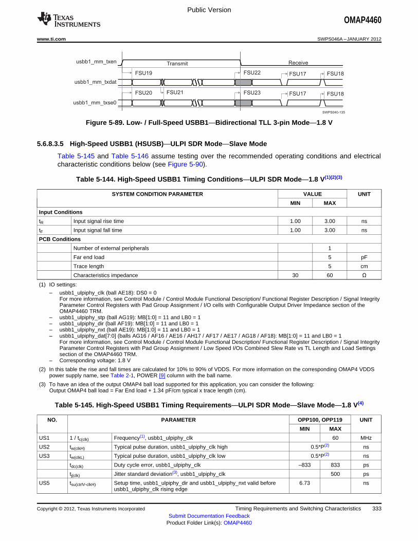
usbb1_mm_txen
usbb1_mm_txdat
usbb1_mm_txse0
Transmit Receive
FSU19
FSU20 FSU21
FSU22
FSU23
FSU17
FSU17
FSU18
FSU18
SWPS040-135
Public Version
OMAP4460
www.ti.com SWPS046A –JANUARY 2012
Figure 5-89. Low- / Full-Speed USBB1—Bidirectional TLL 3-pin Mode—1.8 V
5.6.8.3.5 High-Speed USBB1 (HSUSB)—ULPI SDR Mode—Slave Mode
Table 5-145 and Table 5-146 assume testing over the recommended operating conditions and electricalcharacteristic conditions below (see Figure 5-90).
Table 5-144. High-Speed USBB1 Timing Conditions—ULPI SDR Mode—1.8 V(1)(2)(3)
SYSTEM CONDITION PARAMETER VALUE UNIT
MIN MAX
Input Conditions
tR Input signal rise time 1.00 3.00 ns
tF Input signal fall time 1.00 3.00 ns
PCB Conditions
Number of external peripherals 1
Far end load 5 pF
Trace length 5 cm
Characteristics impedance 30 60 Ω
(1) IO settings:
– usbb1_ulpiphy_clk (ball AE18): DS0 = 0For more information, see Control Module / Control Module Functional Description/ Functional Register Description / Signal IntegrityParameter Control Registers with Pad Group Assignment / I/O cells with Configurable Output Driver Impedance section of theOMAP4460 TRM.
– usbb1_ulpiphy_stp (ball AG19): MB[1:0] = 11 and LB0 = 1– usbb1_ulpiphy_dir (ball AF19): MB[1:0] = 11 and LB0 = 1– usbb1_ulpiphy_nxt (ball AE19): MB[1:0] = 11 and LB0 = 1– usbb1_ulpiphy_dat[7:0] (balls AG16 / AF16 / AE16 / AH17 / AF17 / AE17 / AG18 / AF18): MB[1:0] = 11 and LB0 = 1
For more information, see Control Module / Control Module Functional Description/ Functional Register Description / Signal IntegrityParameter Control Registers with Pad Group Assignment / Low Speed I/Os Combined Slew Rate vs TL Length and Load Settingssection of the OMAP4460 TRM.
– Corresponding voltage: 1.8 V
(2) In this table the rise and fall times are calculated for 10% to 90% of VDDS. For more information on the corresponding OMAP4 VDDSpower supply name, see Table 2-1, POWER [9] column with the ball name.
(3) To have an idea of the output OMAP4 ball load supported for this application, you can consider the following:Output OMAP4 ball load = Far End load + 1.34 pF/cm typical x trace length (cm).
Table 5-145. High-Speed USBB1 Timing Requirements—ULPI SDR Mode—Slave Mode—1.8 V(4)
NO. PARAMETER OPP100, OPP119 UNIT
MIN MAX
US1 1 / tc(clk) Frequency(1), usbb1_ulpiphy_clk 60 MHz
US2 tw(clkH) Typical pulse duration, usbb1_ulpiphy_clk high 0.5*P(2) ns
US3 tw(clkL) Typical pulse duration, usbb1_ulpiphy_clk low 0.5*P(2) ns
tdc(clk) Duty cycle error, usbb1_ulpiphy_clk –833 833 ps
tj(clk) Jitter standard deviation(3), usbb1_ulpiphy_clk 500 ps
US5 tsu(ctrlV-clkH) Setup time, usbb1_ulpiphy_dir and usbb1_ulpiphy_nxt valid before 6.73 nsusbb1_ulpiphy_clk rising edge
Copyright © 2012, Texas Instruments Incorporated Timing Requirements and Switching Characteristics 333Submit Documentation Feedback
Product Folder Link(s): OMAP4460

usbb1_ulpiphy_clk
usbb1_ulpiphy_stp
usbb1_ulpiphy_dirusbb1_ulpiphy_nxt
usbb1_ulpiphy_dat[7:0]
US1
US8US9
US9
US2
US4 US4
US5US6
Data_IN Data_OUT
US3
US7
SWPS040-136
Public Version
OMAP4460
SWPS046A –JANUARY 2012 www.ti.com
Table 5-145. High-Speed USBB1 Timing Requirements—ULPI SDR Mode—Slave Mode—1.8V(4) (continued)
NO. PARAMETER OPP100, OPP119 UNIT
MIN MAX
US6 th(clkH-ctrlV) Hold time, usbb1_ulpiphy_dir and usbb1_ulpiphy_nxt valid after 0.00 nsusbb1_ulpiphy_clk rising edge
US7 tsu(dV-clkH) Setup time, input usbb1_ulpiphy_dat[7:0] valid before 6.73 nsusbb1_ulpiphy_clk rising edge
US8 th(clkH-dV) Hold time, input usbb1_ulpiphy_dat[7:0] valid after usbb1_ulpiphy_clk 0.00 nsrising edge
(1) Related to the input maximum frequency supported by the USB module.
(2) P = clk period in ns
(3) Maximum cycle jitter supported by clk input clock.
(4) See DM Operating Condition Addendum for CORE OPP voltages.
Table 5-146. High-Speed USBB1 Switching Characteristics—ULPI SDR Mode—Slave Mode—1.8 V(1)
NO. PARAMETER OPP100, OPP119 UNIT
MIN MAX
Ball: AE18 (usbb1_ulpiphy_clk)
US4 td(clkL-ctrlV) Delay time, usbb1_ulpiphy_clk rising edge high to output 0.40 8.34 nsusbb1_ulpiphy_stp valid
US9 td(clkL-doV) Delay time, usbb1_ulpiphy_clk rising edge to output 0.40 8.34 nsusbb1_ulpiphy_dat[7:0] valid
Balls: AG19 / AF19 / AE19 / AF18 / AG18 / AE17 / AF17 / AH17 / AE16 / AF16 / AG16(usbb1_ulpiphy_stp, usbb1_ulpiphy_dir, usbb1_ulpiphy_nxt, usbb1_ulpiphy_dat[7:0])
US4 td(clkL-ctrlV) Delay time, usbb1_ulpiphy_clk rising edge high to output 0.22 8.60 nsusbb1_ulpiphy_stp valid
tR(ctrl) Rise time, output usbb1_ulpiphy_stp 3.0 ps
tF(dtrl) Fall time, output usbb1_ulpiphy_stp 3.0 ps
US9 td(clkL-doV) Delay time, usbb1_ulpiphy_clk rising edge to output 0.22 8.60 nsusbb1_ulpiphy_dat[7:0] valid
tR(do) Rise time, output usbb1_ulpiphy_dat[7:0] 3.0 ps
tF(do) Fall time, output usbb1_ulpiphy_dat[7:0] 3.0 ps
(1) See DM Operating Condition Addendum for CORE OPP voltages.
Figure 5-90. High-Speed USBB1—ULPI SDR Mode—Slave Mode—1.8 V
5.6.8.3.6 High-Speed USBB1 (HSUSB)—ULPI TLL Mode—Master Mode
Table 5-148 and Table 5-149 assume testing over the recommended operating conditions and electricalcharacteristic conditions below (see Figure 5-91).
334 Timing Requirements and Switching Characteristics Copyright © 2012, Texas Instruments Incorporated
Submit Documentation FeedbackProduct Folder Link(s): OMAP4460

Public Version
OMAP4460
www.ti.com SWPS046A –JANUARY 2012
Table 5-147. High-Speed USBB1 Timing Conditions—ULPI TLL Mode—Master Mode—1.8 V(1)(2)(3)
SYSTEM CONDITION PARAMETER VALUE UNIT
MIN MAX
Input Conditions
tR Input signal rise time 1.00 3.00 ns
tF Input signal fall time 1.00 3.00 ns
PCB Conditions
Number of external peripherals 1
Far end load 5 pF
Trace length 5 cm
Characteristics impedance 30 60 Ω
(1) IO settings:
– usbb1_ulpitll_clk (ball AE18): DS0 = 0For more information, see Control Module / Control Module Functional Description/ Functional Register Description / Signal IntegrityParameter Control Registers with Pad Group Assignment / I/O cells with Configurable Output Driver Impedance section of theOMAP4460 TRM.
– usbb1_ulpitll_stp (ball AG19): MB[1:0] = 11 and LB0 = 1– usbb1_ulpitll_dir (ball AF19): MB[1:0] = 11 and LB0 = 1– usbb1_ulpitll_nxt (ball AE19): MB[1:0] = 11 and LB0 = 1– usbb1_ulpitll_dat[7:0] (balls AG16 / AF16 / AE16 / AH17 / AF17 / AE17 / AG18 / AF18): MB[1:0] = 11 and LB0 = 1
For more information, see Control Module / Control Module Functional Description/ Functional Register Description / Signal IntegrityParameter Control Registers with Pad Group Assignment / Low Speed I/Os Combined Slew Rate vs TL Length and Load Settingssection of the OMAP4460 TRM.
– Corresponding voltage: 1.8 V
(2) In this table the rise and fall times are calculated for 10% to 90% of VDDS. For more information on the corresponding OMAP4 VDDSpower supply name, see Table 2-1, POWER [9] column with the ball name.
(3) To have an idea of the output OMAP4 ball load supported for this application, you can consider the following:Output OMAP4 ball load = Far End load + 1.34 pF/cm typical x trace length (cm).
Table 5-148. High-Speed USBB1 Timing Requirements—ULPI TLL Mode—Master Mode—1.8 V(1)
NO. PARAMETER OPP100, OPP119 OPP50 UNIT
MIN MAX MIN MAX
For ball: AE18 (usbb1_ulpitll_clk)
UT4 tsu(ctrlV-clkH) Setup time, usbb1_ulpitll_stp valid before 5.78 5.78 nsusbb1_ulpitll_clk rising edge
UT5 th(clkH-ctrlV) Hold time, usbb1_ulpitll_stp valid after 0.09 0.09 nsusbb1_ulpitll_clk rising edge
UT6 tsu(dV-clkH) Setup time, usbb1_ulpitll_dat[7:0] valid before 5.78 5.78 nsusbb1_ulpitll_clk rising edge
UT7 th(clkH-dV) Hold time, usbb1_ulpitll_dat[7:0] valid after 0.09 0.09 nsusbb1_ulpitll_clk rising edge
For balls: AG19 / AF19 / AE19 / AF18 / AG18 / AE17 / AF17 / AH17 / AE16 / AF16 / AG16(usbb1_ulpitll_stp, usbb1_ulpitll_dir, usbb1_ulpitll_nxt, usbb1_ulpitll_dat[7:0])
UT4 tsu(ctrlV-clkH) Setup time, usbb1_ulpitll_stp valid before 5.86 5.86 nsusbb1_ulpitll_clk rising edge
UT5 th(clkH-ctrlV) Hold time, usbb1_ulpitll_stp valid after 0.13 0.13 nsusbb1_ulpitll_clk rising edge
UT6 tsu(dV-clkH) Setup time, usbb1_ulpitll_dat[7:0] valid before 5.86 5.86 nsusbb1_ulpitll_clk rising edge
UT7 th(clkH-dV) Hold time, usbb1_ulpitll_dat[7:0] valid after 0.13 0.13 nsusbb1_ulpitll_clk rising edge
Copyright © 2012, Texas Instruments Incorporated Timing Requirements and Switching Characteristics 335Submit Documentation Feedback
Product Folder Link(s): OMAP4460
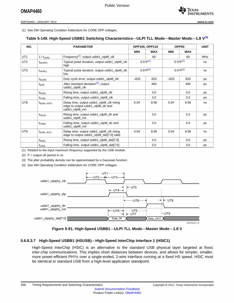
usbb1_ulpiphy_clk
usbb1_ulpiphy_stp
usbb1_ulpiphy_dirusbb1_ulpiphy_nxt
usbb1_ulpiphy_dat[7:0]
UT1
UT7UT9
UT9
UT2
UT5
UT8 UT8
Data_IN Data_OUT
UT3
UT6
SWPS040-137
UT4
Public Version
OMAP4460
SWPS046A –JANUARY 2012 www.ti.com
(1) See DM Operating Condition Addendum for CORE OPP voltages.
Table 5-149. High-Speed USBB1 Switching Characteristics—ULPI TLL Mode—Master Mode—1.8 V(4)
NO. PARAMETER OPP100, OPP119 OPP50 UNIT
MIN MAX MIN MAX
UT1 1 / tc(clk) Frequency(1), output usbb1_ulpitll_clk 60 60 MHz
UT2 tw(clkH) Typical pulse duration, output usbb1_ulpitll_clk 0.5*P(2) 0.5*P(2) nshigh
UT3 tw(clkL) Typical pulse duration, output usbb1_ulpitll_clk 0.5*P(2) 0.5*P(2) nslow
tdc(clk) Duty cycle error, output usbb1_ulpitll_clk –833 833 –833 833 ps
tj(clk) Jitter standard deviation(3), output 400 400 psusbb1_ulpitll_clk
tR(clk) Rising time, output usbb1_ulpitll_clk 3.0 3.0 ps
tF(clk) Falling time, output usbb1_ulpitll_clk 3.0 3.0 ps
UT8 td(clkL-ctrlV) Delay time, output usbb1_ulpitll_clk rising 0.04 8.96 0.04 8.96 nsedge to output usbb1_ulpitll_dir andusbb1_ulpitll_nxt
tR(ctrl) Rising time, output usbb1_ulpitll_dir and 3.0 3.0 psusbb1_ulpitll_nxt
tF(dtrl) Falling time, output usbb1_ulpitll_dir and 3.0 3.0 psusbb1_ulpitll_nxt
UT9 td(clkL-doV) Delay time, output usbb1_ulpitll_clk rising 0.04 8.96 0.04 8.96 nsedge to output usbb1_ulpitll_dat[7:0] valid
tR(do) Rising time, output usbb1_ulpitll_dat[7:0] 3.0 3.0 ps
tF(do) Falling time, output usbb1_ulpitll_dat[7:0] 3.0 3.0 ps
(1) Related to the input maximum frequency supported by the USB module.
(2) P = output clk period in ns
(3) The jitter probability density can be approximated by a Gaussian function.
(4) See DM Operating Condition Addendum for CORE OPP voltages.
Figure 5-91. High-Speed USBB1—ULPI TLL Mode—Master Mode—1.8 V
5.6.8.3.7 High-Speed USBB1 (HSUSB)—High-Speed InterChip Interface 1 (HSIC1)
High-Speed InterChip (HSIC) is an alternative to the standard USB physical layer targeted at fixed,inter-chip communications. This implies short distances between devices, and allows for simpler, smaller,more power-efficient PHYs over a single-ended, 2-wire interface running at a fixed HS speed. HSIC mustbe identical to standard USB from a high-level application standpoint.
336 Timing Requirements and Switching Characteristics Copyright © 2012, Texas Instruments Incorporated
Submit Documentation FeedbackProduct Folder Link(s): OMAP4460
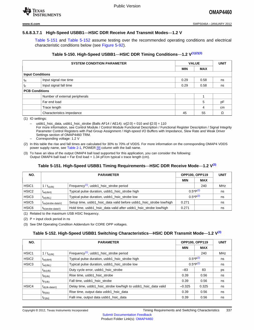
Public Version
OMAP4460
www.ti.com SWPS046A –JANUARY 2012
5.6.8.3.7.1 High-Speed USBB1—HSIC DDR Receive And Transmit Modes—1.2 V
Table 5-151 and Table 5-152 assume testing over the recommended operating conditions and electricalcharacteristic conditions below (see Figure 5-92).
Table 5-150. High-Speed USBB1—HSIC DDR Timing Conditions—1.2 V(1)(2)(3)
SYSTEM CONDITION PARAMETER VALUE UNIT
MIN MAX
Input Conditions
tR Input signal rise time 0.29 0.58 ns
tF Input signal fall time 0.29 0.58 ns
PCB Conditions
Number of external peripherals 1
Far end load 5 pF
Trace length 4 cm
Characteristics impedance 45 55 Ω
(1) IO settings:
– usbb1_hsic_data, usbb1_hsic_strobe (Balls AF14 / AE14): sr[2:0] = 010 and i[2:0] = 110For more information, see Control Module / Control Module Functional Description / Functional Register Description / Signal IntegrityParameter Control Registers with Pad Group Assignment / High-speed I/O Buffers with Impedance, Slew Rate and Weak DriverSettings section of OMAP4460 TRM.
– Corresponding voltage: 1.2 V
(2) In this table the rise and fall times are calculated for 30% to 70% of VDDS. For more information on the corresponding OMAP4 VDDSpower supply name, see Table 2-1, POWER [9] column with the ball name.
(3) To have an idea of the output OMAP4 ball load supported for this application, you can consider the following:Output OMAP4 ball load = Far End load + 1.34 pF/cm typical x trace length (cm).
Table 5-151. High-Speed USBB1 Timing Requirements—HSIC DDR Receive Mode—1.2 V(3)
NO. PARAMETER OPP100, OPP119 UNIT
MIN MAX
HSIC1 1 / tc(clk) Frequency(1), usbb1_hsic_strobe period 240 MHz
HSIC2 tw(clkH) Typical pulse duration, usbb1_hsic_strobe high 0.5*P(2) ns
HSIC3 tw(clkL) Typical pulse duration, usbb1_hsic_strobe low 0.5*P(2) ns
HSIC5 tsu(strobe-dataV) Setup time, usbb1_hsic_data valid before usbb1_hsic_strobe low/high 0.271 ns
HSIC6 th(strobe-dataV) Hold time, usbb1_hsic_data valid after usbb1_hsic_strobe low/high 0.271 ns
(1) Related to the maximum USB HSIC frequency.
(2) P = input clock period in ns
(3) See DM Operating Condition Addendum for CORE OPP voltages.
Table 5-152. High-Speed USBB1 Switching Characteristics—HSIC DDR Transmit Mode—1.2 V(3)
NO. PARAMETER OPP100, OPP119 UNIT
MIN MAX
HSIC1 1 / tc(clk) Frequency(1), usbb1_hsic_strobe period 240 MHz
HSIC2 tw(clkH) Typical pulse duration, usbb1_hsic_strobe high 0.5*P(2) ns
HSIC3 tw(clkL) Typical pulse duration, usbb1_hsic_strobe low 0.5*P(2) ns
tdc(clk) Duty cycle error, usbb1_hsic_strobe –83 83 ps
tR(clk) Rise time, usbb1_hsic_strobe 0.39 0.56 ns
tF(clk) Fall time, usbb1_hsic_strobe 0.39 0.56 ns
HSIC4 td(clk-dataV) Delay time, usbb1_hsic_strobe low/high to usbb1_hsic_data valid –0.325 0.325 ns
tR(do) Rise time, output data usbb1_hsic_data 0.39 0.56 ns
tF(do) Falli ime, output data usbb1_hsic_data 0.39 0.56 ns
Copyright © 2012, Texas Instruments Incorporated Timing Requirements and Switching Characteristics 337Submit Documentation Feedback
Product Folder Link(s): OMAP4460
SWPS040-149
SLIMBUS_CLK
SLIMBUS_DATA
SB2 SB3
SB1
SB4 SB5
Public Version
OMAP4460
SWPS046A –JANUARY 2012 www.ti.com
(1) Related to the maximum USB HSIC frequency.
(2) P = output clock period in ns
(3) See DM Operating Condition Addendum for CORE OPP voltages.
Figure 5-92. High-Speed USBB1—HSIC DDR Receive And Transmit Modes—1.2 V
5.6.8.4 Universal Serial Bus (USB)—USBB2
NOTEFor more information, see the Serial Communication Interface / High-Speed Multiport USBHost Subsystem section of the OMAP4460 TRM.
5.6.8.4.1 Low- / Full-Speed USBB2 (FSUSB)—Bidirectional Standard 4-pin Mode
Table 5-154 and Table 5-155 assume testing over the recommended operating conditions and electricalcharacteristic conditions below (see Figure 5-93).
Table 5-153. Low- / Full-Speed USBB2 Timing Conditions—Bidirectional Standard 4-pin Mode—1.8 V(1)(2)(3)
TIMING CONDITION PARAMETER VALUE UNIT
MIN MAX
Input Conditions
tR Input signal rise time 2 ns
tF Input signal fall time 2 ns
PCB Conditions
Number of external peripherals 1
Far end load 10 pF
Trace length 10 cm
Characteristics impedance 30 60 Ω
(1) IO settings:
– usbb2_mm_txen (ball AC28): MB[1:0] = 10, LB0 = 1– usbb2_mm_txdat (ball AF24): MB[1:0] = 10, LB0 = 1– usbb2_mm_txse0 (ball AE24): MB[1:0] = 10, LB0 = 1– usbb2_mm_rxrcv (ball AD25): MB[1:0] = 10, LB0 = 1
For more information, see Control Module / Control Module Functional Description/ Functional Register Description / Signal IntegrityParameter Control Registers with Pad Group Assignment / 50-Ω Output Buffer I/Os with Combined Mode and Load Settings sectionof the OMAP4460 TRM.
– Corresponding voltage: 1.8 V
(2) In this table the rise and fall times are calculated for 10% to 90% of VDDS. For more information on the corresponding OMAP4 VDDSpower supply name, see Table 2-1, POWER [9] column with the ball name.
(3) To have an idea of the output OMAP4 ball load supported for this application, you can consider the following:Output OMAP4 ball load = Far End load + 1.34 pF/cm typical x trace length (cm).
338 Timing Requirements and Switching Characteristics Copyright © 2012, Texas Instruments Incorporated
Submit Documentation FeedbackProduct Folder Link(s): OMAP4460
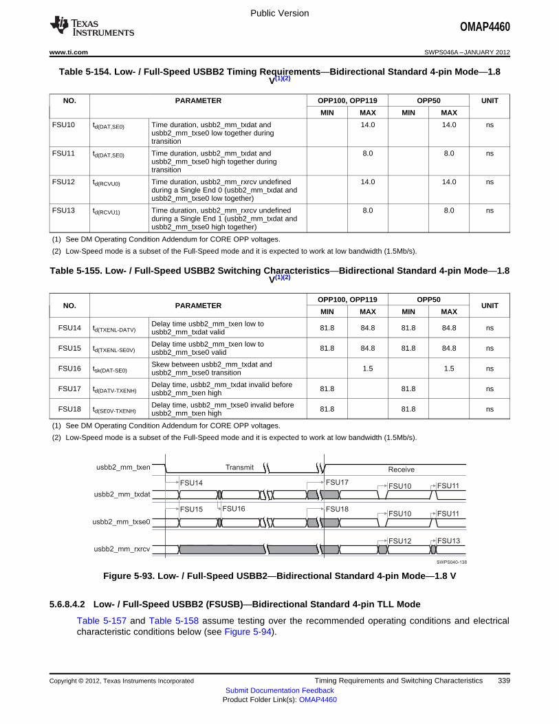
usbb2_mm_txen
usbb2_mm_txdat
usbb2_mm_txse0
usbb2_mm_rxrcv
Transmit Receive
FSU14
FSU15 FSU16
FSU17
FSU18
FSU10
FSU10
FSU13FSU12
FSU11
FSU11
SWPS040-138
Public Version
OMAP4460
www.ti.com SWPS046A –JANUARY 2012
Table 5-154. Low- / Full-Speed USBB2 Timing Requirements—Bidirectional Standard 4-pin Mode—1.8V(1)(2)
NO. PARAMETER OPP100, OPP119 OPP50 UNIT
MIN MAX MIN MAX
FSU10 td(DAT,SE0) Time duration, usbb2_mm_txdat and 14.0 14.0 nsusbb2_mm_txse0 low together duringtransition
FSU11 td(DAT,SE0) Time duration, usbb2_mm_txdat and 8.0 8.0 nsusbb2_mm_txse0 high together duringtransition
FSU12 td(RCVU0) Time duration, usbb2_mm_rxrcv undefined 14.0 14.0 nsduring a Single End 0 (usbb2_mm_txdat andusbb2_mm_txse0 low together)
FSU13 td(RCVU1) Time duration, usbb2_mm_rxrcv undefined 8.0 8.0 nsduring a Single End 1 (usbb2_mm_txdat andusbb2_mm_txse0 high together)
(1) See DM Operating Condition Addendum for CORE OPP voltages.
(2) Low-Speed mode is a subset of the Full-Speed mode and it is expected to work at low bandwidth (1.5Mb/s).
Table 5-155. Low- / Full-Speed USBB2 Switching Characteristics—Bidirectional Standard 4-pin Mode—1.8V(1)(2)
OPP100, OPP119 OPP50NO. PARAMETER UNIT
MIN MAX MIN MAX
Delay time usbb2_mm_txen low toFSU14 td(TXENL-DATV) 81.8 84.8 81.8 84.8 nsusbb2_mm_txdat valid
Delay time usbb2_mm_txen low toFSU15 td(TXENL-SE0V) 81.8 84.8 81.8 84.8 nsusbb2_mm_txse0 valid
Skew between usbb2_mm_txdat andFSU16 tsk(DAT-SE0) 1.5 1.5 nsusbb2_mm_txse0 transition
Delay time, usbb2_mm_txdat invalid beforeFSU17 td(DATV-TXENH) 81.8 81.8 nsusbb2_mm_txen high
Delay time, usbb2_mm_txse0 invalid beforeFSU18 td(SE0V-TXENH) 81.8 81.8 nsusbb2_mm_txen high
(1) See DM Operating Condition Addendum for CORE OPP voltages.
(2) Low-Speed mode is a subset of the Full-Speed mode and it is expected to work at low bandwidth (1.5Mb/s).
Figure 5-93. Low- / Full-Speed USBB2—Bidirectional Standard 4-pin Mode—1.8 V
5.6.8.4.2 Low- / Full-Speed USBB2 (FSUSB)—Bidirectional Standard 4-pin TLL Mode
Table 5-157 and Table 5-158 assume testing over the recommended operating conditions and electricalcharacteristic conditions below (see Figure 5-94).
Copyright © 2012, Texas Instruments Incorporated Timing Requirements and Switching Characteristics 339Submit Documentation Feedback
Product Folder Link(s): OMAP4460

Public Version
OMAP4460
SWPS046A –JANUARY 2012 www.ti.com
Table 5-156. Low- / Full-Speed USBB2 Timing Conditions—Bidirectional TLL 4-pin Mode—1.8 V(1)(2)(3)
TIMING CONDITION PARAMETER VALUE UNIT
MIN MAX
Input Conditions
tR Input signal rise time 2 ns
tF Input signal fall time 2 ns
PCB Conditions
Number of external peripherals 1
Far end load 10 pF
Trace length 10 cm
Characteristics impedance 30 60 Ω
(1) IO settings:
– usbb2_mm_txen (ball AC28): MB[1:0] = 10, LB0 = 1– usbb2_mm_txdat (ball AF24): MB[1:0] = 10, LB0 = 1– usbb2_mm_txse0 (ball AE24): MB[1:0] = 10, LB0 = 1– usbb2_mm_rxrcv (ball AD25): MB[1:0] = 10, LB0 = 1
For more information, see Control Module / Control Module Functional Description/ Functional Register Description / Signal IntegrityParameter Control Registers with Pad Group Assignment / 50-Ω Output Buffer I/Os with Combined Mode and Load Settings sectionof the OMAP4460 TRM.
– Corresponding voltage: 1.8 V
(2) In this table the rise and fall times are calculated for 10% to 90% of VDDS. For more information on the corresponding OMAP4 VDDSpower supply name, see Table 2-1, POWER [9] column with the ball name.
(3) To have an idea of the output OMAP4 ball load supported for this application, you can consider the following:Output OMAP4 ball load = Far End load + 1.34 pF/cm typical x trace length (cm).
Table 5-157. Low- / Full-Speed USBB2 Timing Requirements—Bidirectional TLL 4-pin Mode—1.8 V(1)(2)
NO. PARAMETER OPP100, OPP119 OPP50 UNIT
MIN MAX MIN MAX
FSU9 td(DAT,SE0) Time duration, usbb2_mm_txdat and 14.0 14.0 nsusbb2_mm_txse0 low together duringtransition
FSU10 td(DAT,SE0) Time duration, usbb2_mm_txdat and 8.0 8.0 nsusbb2_mm_txse0 high together duringtransition
(1) See DM Operating Condition Addendum for CORE OPP voltages.
(2) Low-Speed mode is a subset of the Full-Speed mode and it is expected to work at low bandwidth (1.5Mb/s).
Table 5-158. Low- / Full-Speed USBB2 Switching Characteristics—Bidirectional TLL 4-pin Mode—1.8V(1)(2)
NO. PARAMETER OPP100, OPP119 OPP50 UNIT
MIN MAX MIN MAX
FSU11 td(TXENL-DATV) Delay time usbb2_mm_txen low to 81.8 84.8 81.8 84.8 nsusbb2_mm_txdat valid
FSU12 td(TXENL-SE0V) Delay time usbb2_mm_txen low to 81.8 84.8 81.8 84.8 nsusbb2_mm_txse0 valid
FSU13 tsk(DAT-SE0) Skew between usbb2_mm_txdat and 1.5 1.5 nsusbb2_mm_txse0 transition
FSU14 tsk(DAT-SE0) Skew between usbb2_mm_txdat, 1.5 1.5 nsusbb2_mm_txse0 and usbb2_mm_rxrcvtransition
FSU15 td(DATV-TXENH) Delay time, usbb2_mm_txdat invalid before 81.8 81.8 nsusbb2_mm_txen high
FSU16 td(SE0V-TXENH) Delay time, usbb2_mm_txse0 invalid before 81.8 81.8 nsusbb2_mm_txen high
340 Timing Requirements and Switching Characteristics Copyright © 2012, Texas Instruments Incorporated
Submit Documentation FeedbackProduct Folder Link(s): OMAP4460

usbb2_mm_txen
usbb2_mm_txdat
usbb2_mm_txse0
usbb2_mm_rxrcv
Transmit Receive
FSU11
FSU12 FSU13
FSU15
FSU16
FSU9
FSU9
FSU10
FSU10
SWPS040-139
FSU14
Public Version
OMAP4460
www.ti.com SWPS046A –JANUARY 2012
(1) See DM Operating Condition Addendum for CORE OPP voltages.
(2) Low-Speed mode is a subset of the Full-Speed mode and it is expected to work at low bandwidth (1.5Mb/s).
Figure 5-94. Low- / Full-Speed USBB2—Bidirectional TLL 4-pin Mode—1.8 V
5.6.8.4.3 Low- / Full-Speed USBB2 (FSUSB)—Bidirectional Standard 3-pin Mode
Table 5-160 and Table 5-161 assume testing over the recommended operating conditions and electricalcharacteristic conditions below (see Figure 5-95).
Table 5-159. Low- / Full-Speed USBB2 Timing Conditions—Bidirectional Standard 3-pin Mode—1.8 V(1)(2)(3)
TIMING CONDITION PARAMETER VALUE UNIT
MIN MAX
Input Conditions
tR Input signal rise time 2 ns
tF Input signal fall time 2 ns
PCB Conditions
Number of external peripherals 1
Far end load 10 pF
Trace length 10 cm
Characteristics impedance 30 60 Ω
(1) IO settings:
– usbb2_mm_txen (ball AE11): DS0 = 0– usbb2_mm_txdat (ball AF11): DS0 = 0– usbb2_mm_txse0 (ball AG11): DS0 = 0
For more information, see Control Module / Control Module Functional Description/ Functional Register Description / Signal IntegrityParameter Control Registers with Pad Group Assignment / I/O cells with Configurable Output Driver Impedance section of theOMAP4460 TRM.
– Corresponding voltage: 1.8 V
(2) In this table the rise and fall times are calculated for 10% to 90% of VDDS. For more information on the corresponding OMAP4 VDDSpower supply name, see Table 2-1, POWER [9] column with the ball name.
(3) To have an idea of the output OMAP4 ball load supported for this application, you can consider the following:Output OMAP4 ball load = Far End load + 1.34 pF/cm typical x trace length (cm).
Table 5-160. Low- / Full-Speed USBB2 Timing Requirements—Bidirectional Standard 3-pin Mode—1.8V(1)(2)
NO. PARAMETER OPP100, OPP119 OPP50 UNIT
MIN MAX MIN MAX
FSU19 td(DAT,SE0) Time duration, usbb2_mm_txdat and 14.0 14.0 nsusbb2_mm_txse0 low together duringtransition
FSU20 td(DAT,SE0) Time duration, usbb2_mm_txdat and 8.0 8.0 nsusbb2_mm_txse0 high together duringtransition
Copyright © 2012, Texas Instruments Incorporated Timing Requirements and Switching Characteristics 341Submit Documentation Feedback
Product Folder Link(s): OMAP4460

usbb2_mm_txen
usbb2_mm_txdat
usbb2_mm_txse0
Transmit Receive
FSU21
FSU22 FSU23
FSU24
FSU25
FSU19
FSU19
FSU20
FSU20
SWPS040-140
Public Version
OMAP4460
SWPS046A –JANUARY 2012 www.ti.com
(1) See DM Operating Condition Addendum for CORE OPP voltages.
(2) Low-Speed mode is a subset of the Full-Speed mode and it is expected to work at low bandwidth (1.5Mb/s).
Table 5-161. Low- / Full-Speed USBB2 Switching Characteristics—Bidirectional Standard 3-pin Mode—1.8V(1)(2)
NO. PARAMETER OPP100, OPP119 OPP50 UNIT
MIN MAX MIN MAX
FSU21 td(TXENL-DATV) Delay time usbb2_mm_txen low to 81.8 84.8 81.8 84.8 nsusbb2_mm_txdat valid
FSU22 td(TXENL-SE0V) Delay time usbb2_mm_txen low to 81.8 84.8 81.8 84.8 nsusbb2_mm_txse0 valid
FSU23 tsk(DAT-SE0) Skew between usbb2_mm_txdat and 1.5 1.5 nsusbb2_mm_txse0 transition
FSU24 td(DATV-TXENH) Delay time, usbb2_mm_txdat invalid before 81.8 81.8 nsusbb2_mm_txen high
FSU25 td(SE0V-TXENH) Delay time, usbb2_mm_txse0 invalid before 81.8 81.8 nsusbb2_mm_txen high
(1) See DM Operating Condition Addendum for CORE OPP voltages.
(2) Low-Speed mode is a subset of the Full-Speed mode and it is expected to work at low bandwidth (1.5Mb/s).
Figure 5-95. Low- / Full-Speed USBB2—Bidirectional Standard 3-pin Mode—1.8 V
5.6.8.4.4 Low- / Full-Speed USBB2 (FSUSB)—Bidirectional Standard 3-pin TLL Mode
Table 5-163 and Table 5-164 assume testing over the recommended operating conditions and electricalcharacteristic conditions below (see Figure 5-96).
Table 5-162. Low- / Full-Speed USBB2 Timing Conditions—Bidirectional TLL 3-pin Mode—1.8 V(1)(2)(3)
TIMING CONDITION PARAMETER VALUE UNIT
MIN MAX
Input Conditions
tR Input signal rise time 2 ns
tF Input signal fall time 2 ns
PCB Conditions
Number of external peripherals 1
Far end load 10 pF
Trace length 10 cm
Characteristics impedance 30 60 Ω
(1) IO settings:
– usbb2_mm_txen (ball AE11): DS0 = 0– usbb2_mm_txdat (ball AF11): DS0 = 0– usbb2_mm_txse0 (ball AG11): DS0 = 0
For more information, see Control Module / Control Module Functional Description/ Functional Register Description / Signal IntegrityParameter Control Registers with Pad Group Assignment / I/O cells with Configurable Output Driver Impedance section of theOMAP4460 TRM.
– Corresponding voltage: 1.8 V
342 Timing Requirements and Switching Characteristics Copyright © 2012, Texas Instruments Incorporated
Submit Documentation FeedbackProduct Folder Link(s): OMAP4460
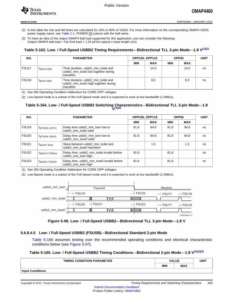
usbb2_mm_txen
usbb2_mm_txdat
usbb2_mm_txse0
Transmit Receive
FSU19
FSU20 FSU21
FSU22
FSU23
FSU17
FSU17
FSU18
FSU18
SWPS040-141
Public Version
OMAP4460
www.ti.com SWPS046A –JANUARY 2012
(2) In this table the rise and fall times are calculated for 10% to 90% of VDDS. For more information on the corresponding OMAP4 VDDSpower supply name, see Table 2-1, POWER [9] column with the ball name.
(3) To have an idea of the output OMAP4 ball load supported for this application, you can consider the following:Output OMAP4 ball load = Far End load + 1.34 pF/cm typical x trace length (cm).
Table 5-163. Low- / Full-Speed USBB2 Timing Requirements—Bidirectional TLL 3-pin Mode—1.8 V(1)(2)
NO. PARAMETER OPP100, OPP119 OPP50 UNIT
MIN MAX MIN MAX
FSU17 td(DAT,SE0) Time duration, usbb2_mm_txdat and 14.0 14.0 nsusbb2_mm_txse0 low together duringtransition
FSU18 td(DAT,SE0) Time duration, usbb2_mm_txdat and 8.0 8.0 nsusbb2_mm_txse0 high together duringtransition
(1) See DM Operating Condition Addendum for CORE OPP voltages.
(2) Low-Speed mode is a subset of the Full-Speed mode and it is expected to work at low bandwidth (1.5Mb/s).
Table 5-164. Low- / Full-Speed USBB2 Switching Characteristics—Bidirectional TLL 3-pin Mode—1.8V(1)(2)
NO. PARAMETER OPP100, OPP119 OPP50 UNIT
MIN MAX MIN MAX
FSU19 td(TXENL-DATV) Delay time usbb2_mm_txen low to 81.8 84.8 81.8 84.8 nsusbb2_mm_txdat valid
FSU20 td(TXENL-SE0V) Delay time usbb2_mm_txen low to 81.8 84.8 81.8 84.8 nsusbb2_mm_txse0 valid
FSU21 tsk(DAT-SE0) Skew between usbb2_mm_txdat and 1.5 1.5 nsusbb2_mm_txse0 transition
FSU22 td(DATV-TXENH) Delay time, usbb2_mm_txdat invalid before 81.8 81.8 nsusbb2_mm_txen high
FSU23 td(SE0V-TXENH) Delay time, usbb2_mm_txse0 invalid before 81.8 81.8 nsusbb2_mm_txen high
(1) See DM Operating Condition Addendum for CORE OPP voltages.
(2) Low-Speed mode is a subset of the Full-Speed mode and it is expected to work at low bandwidth (1.5Mb/s).
Figure 5-96. Low- / Full-Speed USBB2—Bidirectional TLL 3-pin Mode—1.8 V
5.6.8.4.5 Low- / Full-Speed USBB2 (FSUSB)—Bidirectional Standard 2-pin Mode
Table 5-166 assumes testing over the recommended operating conditions and electrical characteristicconditions below (see Figure 5-97).
Table 5-165. Low- / Full-Speed USBB2 Timing Conditions—Bidirectional 2-pin Mode—1.8 V(1)(2)(3)
TIMING CONDITION PARAMETER VALUE UNIT
MIN MAX
Input Conditions
Copyright © 2012, Texas Instruments Incorporated Timing Requirements and Switching Characteristics 343Submit Documentation Feedback
Product Folder Link(s): OMAP4460

FSU2FSU1
SWPS040-142
usbb2_mm_rxdm
FSU2FSU1
usbb2_mm_rxdp
Public Version
OMAP4460
SWPS046A –JANUARY 2012 www.ti.com
Table 5-165. Low- / Full-Speed USBB2 Timing Conditions—Bidirectional 2-pin Mode—1.8V(1)(2)(3) (continued)
TIMING CONDITION PARAMETER VALUE UNIT
MIN MAX
tR Input signal rise time 2 ns
tF Input signal fall time 2 ns
PCB Conditions
Number of external peripherals 1
Far end load 10 pF
Trace length 10 cm
Characteristics impedance 30 60 Ω
(1) IO settings:
– Balls AD26, AD27 (usbb2_mm_rxdp, usbb2_mm_rxdm): MB[1:0] = 10 and LB0 = 1For more information, see Control Module / Control Module Functional Description/ Functional Register Description / Signal IntegrityParameter Control Registers with Pad Group Assignment / 50-Ω Output Buffer I/Os with Combined Mode and Load Settings sectionof the OMAP4460 TRM.
– Corresponding voltage: 1.8 V
(2) In this table the rise and fall times are calculated for 10% to 90% of VDDS. For more information on the corresponding OMAP4 VDDSpower supply name, see Table 2-1, POWER [9] column with the ball name.
(3) To have an idea of the output OMAP4 ball load supported for this application, you can consider the following:Output OMAP4 ball load = Far End load + 1.34 pF/cm typical x trace length (cm).
Table 5-166. Low- / Full-Speed USBB2 Timing Requirements—Bidirectional 2-pin Mode—1.8 V(1)(2)
NO. PARAMETER OPP100, OPP119 OPP50 UNIT
MIN MAX MIN MAX
FSU1 td(DAT,SE0) Time duration, usbb2_mm_rxdp and 14.0 14.0 nsusbb2_mm_rxdm low together duringtransition
FSU2 td(DAT,SE0) Time duration, usbb2_mm_rxdp and 8.0 8.0 nsusbb2_mm_rxdm high together duringtransition
(1) See DM Operating Condition Addendum for CORE OPP voltages.
(2) Low-Speed mode is a subset of the Full-Speed mode and it is expected to work at low bandwidth (1.5Mb/s).
Figure 5-97. Low- / Full-Speed USBB2—Bidirectional 2-pin Mode—1.8 V
5.6.8.4.6 High-Speed USBB2 (HSUSB)—ULPI SDR Mode—Slave Mode
Table 5-168 and Table 5-169 assume testing over the recommended operating conditions and electricalcharacteristic conditions below (see Figure 5-98).
Table 5-167. High-Speed USBB2 Timing Conditions—ULPI SDR Mode(1)(2)(3)
SYSTEM CONDITION PARAMETER VALUE UNIT
MIN MAX
Input Conditions
tR Input signal rise time 1.00 3.00 ns
tF Input signal fall time 1.00 3.00 ns
PCB Conditions
344 Timing Requirements and Switching Characteristics Copyright © 2012, Texas Instruments Incorporated
Submit Documentation FeedbackProduct Folder Link(s): OMAP4460
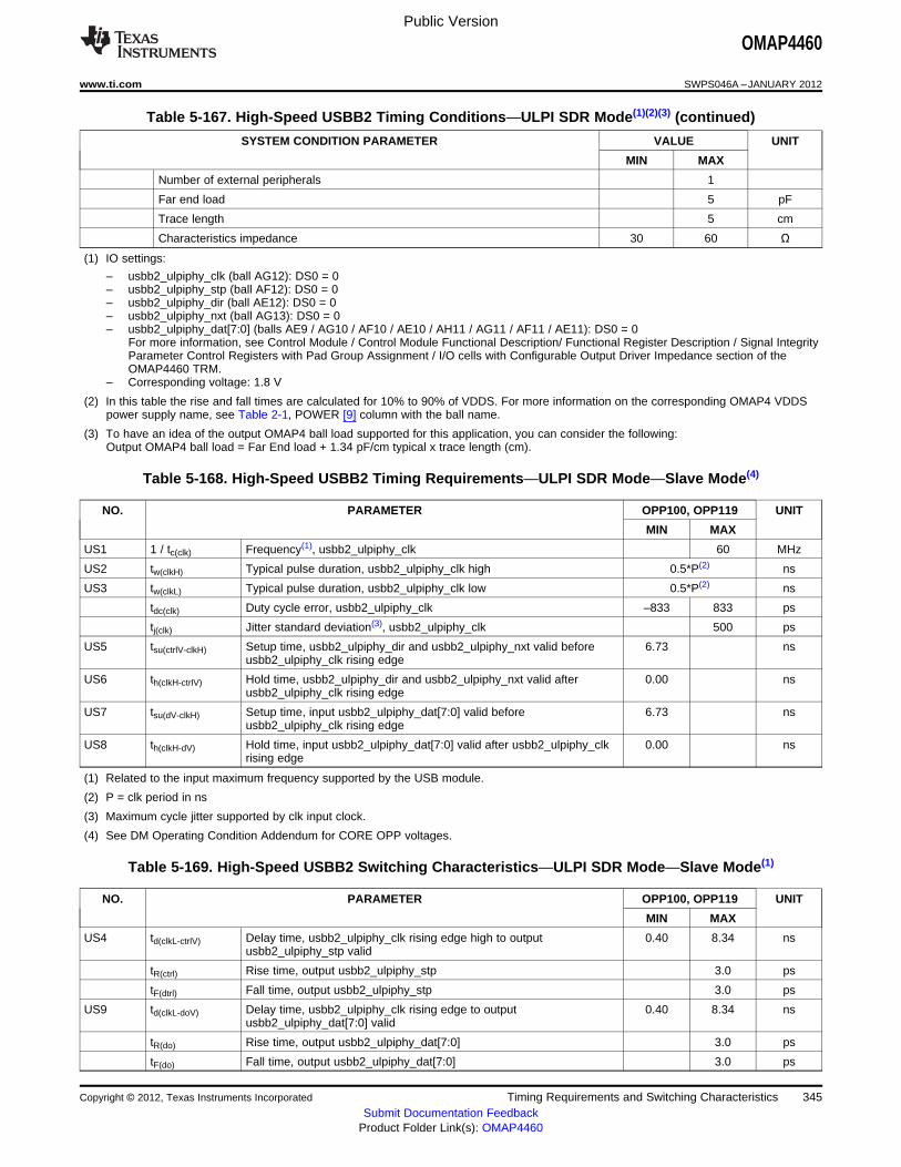
Public Version
OMAP4460
www.ti.com SWPS046A –JANUARY 2012
Table 5-167. High-Speed USBB2 Timing Conditions—ULPI SDR Mode(1)(2)(3) (continued)
SYSTEM CONDITION PARAMETER VALUE UNIT
MIN MAX
Number of external peripherals 1
Far end load 5 pF
Trace length 5 cm
Characteristics impedance 30 60 Ω
(1) IO settings:
– usbb2_ulpiphy_clk (ball AG12): DS0 = 0– usbb2_ulpiphy_stp (ball AF12): DS0 = 0– usbb2_ulpiphy_dir (ball AE12): DS0 = 0– usbb2_ulpiphy_nxt (ball AG13): DS0 = 0– usbb2_ulpiphy_dat[7:0] (balls AE9 / AG10 / AF10 / AE10 / AH11 / AG11 / AF11 / AE11): DS0 = 0
For more information, see Control Module / Control Module Functional Description/ Functional Register Description / Signal IntegrityParameter Control Registers with Pad Group Assignment / I/O cells with Configurable Output Driver Impedance section of theOMAP4460 TRM.
– Corresponding voltage: 1.8 V
(2) In this table the rise and fall times are calculated for 10% to 90% of VDDS. For more information on the corresponding OMAP4 VDDSpower supply name, see Table 2-1, POWER [9] column with the ball name.
(3) To have an idea of the output OMAP4 ball load supported for this application, you can consider the following:Output OMAP4 ball load = Far End load + 1.34 pF/cm typical x trace length (cm).
Table 5-168. High-Speed USBB2 Timing Requirements—ULPI SDR Mode—Slave Mode(4)
NO. PARAMETER OPP100, OPP119 UNIT
MIN MAX
US1 1 / tc(clk) Frequency(1), usbb2_ulpiphy_clk 60 MHz
US2 tw(clkH) Typical pulse duration, usbb2_ulpiphy_clk high 0.5*P(2) ns
US3 tw(clkL) Typical pulse duration, usbb2_ulpiphy_clk low 0.5*P(2) ns
tdc(clk) Duty cycle error, usbb2_ulpiphy_clk –833 833 ps
tj(clk) Jitter standard deviation(3), usbb2_ulpiphy_clk 500 ps
US5 tsu(ctrlV-clkH) Setup time, usbb2_ulpiphy_dir and usbb2_ulpiphy_nxt valid before 6.73 nsusbb2_ulpiphy_clk rising edge
US6 th(clkH-ctrlV) Hold time, usbb2_ulpiphy_dir and usbb2_ulpiphy_nxt valid after 0.00 nsusbb2_ulpiphy_clk rising edge
US7 tsu(dV-clkH) Setup time, input usbb2_ulpiphy_dat[7:0] valid before 6.73 nsusbb2_ulpiphy_clk rising edge
US8 th(clkH-dV) Hold time, input usbb2_ulpiphy_dat[7:0] valid after usbb2_ulpiphy_clk 0.00 nsrising edge
(1) Related to the input maximum frequency supported by the USB module.
(2) P = clk period in ns
(3) Maximum cycle jitter supported by clk input clock.
(4) See DM Operating Condition Addendum for CORE OPP voltages.
Table 5-169. High-Speed USBB2 Switching Characteristics—ULPI SDR Mode—Slave Mode(1)
NO. PARAMETER OPP100, OPP119 UNIT
MIN MAX
US4 td(clkL-ctrlV) Delay time, usbb2_ulpiphy_clk rising edge high to output 0.40 8.34 nsusbb2_ulpiphy_stp valid
tR(ctrl) Rise time, output usbb2_ulpiphy_stp 3.0 ps
tF(dtrl) Fall time, output usbb2_ulpiphy_stp 3.0 ps
US9 td(clkL-doV) Delay time, usbb2_ulpiphy_clk rising edge to output 0.40 8.34 nsusbb2_ulpiphy_dat[7:0] valid
tR(do) Rise time, output usbb2_ulpiphy_dat[7:0] 3.0 ps
tF(do) Fall time, output usbb2_ulpiphy_dat[7:0] 3.0 ps
Copyright © 2012, Texas Instruments Incorporated Timing Requirements and Switching Characteristics 345Submit Documentation Feedback
Product Folder Link(s): OMAP4460
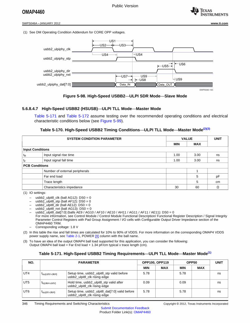
usbb2_ulpiphy_clk
usbb2_ulpiphy_stp
usbb2_ulpiphy_dirusbb2_ulpiphy_nxt
usbb2_ulpiphy_dat[7:0]
US1
US8US9
US9
US2
US4 US4
US5US6
Data_IN Data_OUT
US3
US7
SWPS040-143
Public Version
OMAP4460
SWPS046A –JANUARY 2012 www.ti.com
(1) See DM Operating Condition Addendum for CORE OPP voltages.
Figure 5-98. High-Speed USBB2—ULPI SDR Mode—Slave Mode
5.6.8.4.7 High-Speed USBB2 (HSUSB)—ULPI TLL Mode—Master Mode
Table 5-171 and Table 5-172 assume testing over the recommended operating conditions and electricalcharacteristic conditions below (see Figure 5-99).
Table 5-170. High-Speed USBB2 Timing Conditions—ULPI TLL Mode—Master Mode(2)(3)
SYSTEM CONDITION PARAMETER VALUE UNIT
MIN MAX
Input Conditions
tR Input signal rise time 1.00 3.00 ns
tF Input signal fall time 1.00 3.00 ns
PCB Conditions
Number of external peripherals 1
Far end load 5 pF
Trace length 5 cm
Characteristics impedance 30 60 Ω
(1) IO settings:
– usbb2_ulpitll_clk (ball AG12): DS0 = 0– usbb2_ulpitll_stp (ball AF12): DS0 = 0– usbb2_ulpitll_dir (ball AE12): DS0 = 0– usbb2_ulpitll_nxt (ball AG13): DS0 = 0– usbb2_ulpitll_dat[7:0] (balls AE9 / AG10 / AF10 / AE10 / AH11 / AG11 / AF11 / AE11): DS0 = 0
For more information, see Control Module / Control Module Functional Description/ Functional Register Description / Signal IntegrityParameter Control Registers with Pad Group Assignment / I/O cells with Configurable Output Driver Impedance section of theOMAP4460 TRM.
– Corresponding voltage: 1.8 V
(2) In this table the rise and fall times are calculated for 10% to 90% of VDDS. For more information on the corresponding OMAP4 VDDSpower supply name, see Table 2-1, POWER [9] column with the ball name.
(3) To have an idea of the output OMAP4 ball load supported for this application, you can consider the following:Output OMAP4 ball load = Far End load + 1.34 pF/cm typical x trace length (cm).
Table 5-171. High-Speed USBB2 Timing Requirements—ULPI TLL Mode—Master Mode(1)
NO. PARAMETER OPP100, OPP119 OPP50 UNIT
MIN MAX MIN MAX
UT4 tsu(ctrlV-clkH) Setup time, usbb2_ulpitll_stp valid before 5.78 5.78 nsusbb2_ulpitll_clk rising edge
UT5 th(clkH-ctrlV) Hold time, usbb2_ulpitll_stp valid after 0.09 0.09 nsusbb2_ulpitll_clk rising edge
UT6 tsu(dV-clkH) Setup time, usbb2_ulpitll_dat[7:0] valid before 5.78 5.78 nsusbb2_ulpitll_clk rising edge
346 Timing Requirements and Switching Characteristics Copyright © 2012, Texas Instruments Incorporated
Submit Documentation FeedbackProduct Folder Link(s): OMAP4460
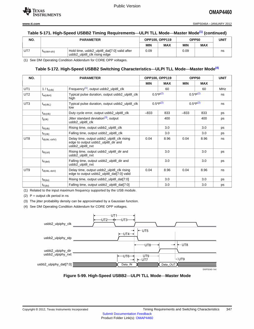
usbb2_ulpiphy_clk
usbb2_ulpiphy_stp
usbb2_ulpiphy_dirusbb2_ulpiphy_nxt
usbb2_ulpiphy_dat[7:0]
UT1
UT7UT9
UT9
UT2
UT5
UT8 UT8
Data_IN Data_OUT
UT3
UT6
SWPS040-144
UT4
Public Version
OMAP4460
www.ti.com SWPS046A –JANUARY 2012
Table 5-171. High-Speed USBB2 Timing Requirements—ULPI TLL Mode—Master Mode(1) (continued)
NO. PARAMETER OPP100, OPP119 OPP50 UNIT
MIN MAX MIN MAX
UT7 th(clkH-dV) Hold time, usbb2_ulpitll_dat[7:0] valid after 0.09 0.09 nsusbb2_ulpitll_clk rising edge
(1) See DM Operating Condition Addendum for CORE OPP voltages.
Table 5-172. High-Speed USBB2 Switching Characteristics—ULPI TLL Mode—Master Mode(4)
NO. PARAMETER OPP100, OPP119 OPP50 UNIT
MIN MAX MIN MAX
UT1 1 / tc(clk) Frequency(1), output usbb2_ulpitll_clk 60 60 MHz
UT2 tw(clkH) Typical pulse duration, output usbb2_ulpitll_clk 0.5*P(2) 0.5*P(2) nshigh
UT3 tw(clkL) Typical pulse duration, output usbb2_ulpitll_clk 0.5*P(2) 0.5*P(2) nslow
tdc(clk) Duty cycle error, output usbb2_ulpitll_clk –833 833 –833 833 ps
tj(clk) Jitter standard deviation(3), output 400 400 psusbb2_ulpitll_clk
tR(clk) Rising time, output usbb2_ulpitll_clk 3.0 3.0 ps
tF(clk) Falling time, output usbb2_ulpitll_clk 3.0 3.0 ps
UT8 td(clkL-ctrlV) Delay time, output usbb2_ulpitll_clk rising 0.04 8.96 0.04 8.96 nsedge to output usbb2_ulpitll_dir andusbb2_ulpitll_nxt
tR(ctrl) Rising time, output usbb2_ulpitll_dir and 3.0 3.0 psusbb2_ulpitll_nxt
tF(dtrl) Falling time, output usbb2_ulpitll_dir and 3.0 3.0 psusbb2_ulpitll_nxt
UT9 td(clkL-doV) Delay time, output usbb2_ulpitll_clk rising 0.04 8.96 0.04 8.96 nsedge to output usbb2_ulpitll_dat[7:0] valid
tR(do) Rising time, output usbb2_ulpitll_dat[7:0] 3.0 3.0 ps
tF(do) Falling time, output usbb2_ulpitll_dat[7:0] 3.0 3.0 ps
(1) Related to the input maximum frequency supported by the USB module.
(2) P = output clk period in ns
(3) The jitter probability density can be approximated by a Gaussian function.
(4) See DM Operating Condition Addendum for CORE OPP voltages.
Figure 5-99. High-Speed USBB2—ULPI TLL Mode—Master Mode
Copyright © 2012, Texas Instruments Incorporated Timing Requirements and Switching Characteristics 347Submit Documentation Feedback
Product Folder Link(s): OMAP4460

Public Version
OMAP4460
SWPS046A –JANUARY 2012 www.ti.com
5.6.8.4.8 High-Speed USBB2 (HSUSB)—High-Speed InterChip Interface 2 (HSIC2)
High-Speed InterChip (HSIC) is an alternative to the standard USB physical layer targeted at fixed,inter-chip communications. This implies short distances between devices, and allows for simpler, smaller,more power-efficient PHYs over a single-ended, 2-wire interface running at a fixed HS speed. HSICshould be identical to standard USB from a high-level application standpoint.
5.6.8.4.8.1 High-Speed USBB2—HSIC DDR Receive And Transmit Modes—1.2 V
Table 5-174 and Table 5-175 assume testing over the recommended operating conditions and electricalcharacteristic conditions below (see Figure 5-100).
Table 5-173. High-Speed USBB2—HSIC DDR Timing Conditions—1.2 V(1)(2)(3)
SYSTEM CONDITION PARAMETER VALUE UNIT
MIN MAX
Input Conditions
tR Input signal rise time 0.29 0.58 ns
tF Input signal fall time 0.29 0.58 ns
PCB Conditions
Number of external peripherals 1
Far end load 5 pF
Trace length 4 cm
Characteristics impedance 45 55 Ω
(1) IO settings:
– usbb2_hsic_data, usbb2_hsic_strobe (balls: AF13, AE13): sr[2:0] = 010 and i[2:0] = 110For more information, see Control Module / Control Module Functional Description / Functional Register Description / Signal IntegrityParameter Control Registers with Pad Group Assignment / High-speed I/O Buffers with Impedance, Slew Rate and Weak DriverSettings section of OMAP4460 TRM.
– Corresponding voltage: 1.2 V
(2) In this table the rise and fall times are calculated for 30% to 70% of VDDS. For more information on the corresponding OMAP4 VDDSpower supply name, see Table 2-1, POWER [9] column with the ball name.
(3) To have an idea of the output OMAP4 ball load supported for this application, you can consider the following:Output OMAP4 ball load = Far End load + 1.34 pF/cm typical x trace length (cm).
Table 5-174. High-Speed USBB2 Timing Requirements—HSIC DDR Receive Mode—1.2 V(3)
NO. PARAMETER OPP100, OPP119 UNIT
MIN MAX
HSIC1 1 / tc(clk) Frequency(1), usbb2_hsic_strobe period 240 MHz
HSIC2 tw(clkH) Typical pulse duration, usbb2_hsic_strobe high 0.5*P(2) ns
HSIC3 tw(clkL) Typical pulse duration, usbb2_hsic_strobe low 0.5*P(2) ns
HSIC5 tsu(strobe-dataV) Setup time, usbb2_hsic_data valid before usbb2_hsic_strobe low/high 0.271 ns
HSIC6 th(strobe-dataV) Hold time, usbb2_hsic_data valid after usbb2_hsic_strobe low/high 0.271 ns
(1) Related to the maximum USB HSIC frequency.
(2) P = input clock period in ns
(3) See DM Operating Condition Addendum for CORE OPP voltages.
Table 5-175. High-Speed USBB2 Switching Characteristics—HSIC DDR Transmit Mode—1.2 V(3)
NO. PARAMETER OPP100, OPP119 UNIT
MIN MAX
HSIC1 1 / tc(clk) Frequency(1), usbb2_hsic_strobe period 240 MHz
HSIC2 tw(clkH) Typical pulse duration, usbb2_hsic_strobe high 0.5*P(2) ns
HSIC3 tw(clkL) Typical pulse duration, usbb2_hsic_strobe low 0.5*P(2) ns
tdc(clk) Duty cycle error, usbb2_hsic_strobe –83 83 ps
348 Timing Requirements and Switching Characteristics Copyright © 2012, Texas Instruments Incorporated
Submit Documentation FeedbackProduct Folder Link(s): OMAP4460

SWPS040-150
SLIMBUS_CLK
SLIMBUS_DATA
SB2 SB3
SB1
SB6
Public Version
OMAP4460
www.ti.com SWPS046A –JANUARY 2012
Table 5-175. High-Speed USBB2 Switching Characteristics—HSIC DDR Transmit Mode—1.2V(3) (continued)
NO. PARAMETER OPP100, OPP119 UNIT
MIN MAX
tR(clk) Rise time, usbb2_hsic_strobe 0.39 0.56 ns
tF(clk) Fall time, usbb2_hsic_strobe 0.39 0.56 ns
HSIC4 td(clk-dataV) Delay time, usbb2_hsic_strobe low/high to usbb2_hsic_data valid –0.325 0.325 ns
tR(do) Rise time, output data usbb2_hsic_data 0.39 0.56 ns
tF(do) Falli ime, output data usbb2_hsic_data 0.39 0.56 ns
(1) Related to the maximum USB HSIC frequency.
(2) P = output clock period in ns
(3) See DM Operating Condition Addendum for CORE OPP voltages.
Figure 5-100. High-Speed USBB2—HSIC DDR Receive And Transmit Modes—1.2 V
5.6.9 Inter-Integrated Circuit Interface (I2C)
NOTEFor more information, see the Serial Communication Interface / Multimaster High-Speed I2CController / HS I2C Functional Description section of the OMAP4460 TRM.
The multi-master I2C peripheral provides an interface between two or more devices via an I2C serial bus.The I2C controller supports the multi-master mode which allows more than one device capable ofcontrolling the bus to be connected to it. Each I2C device is recognized by a unique address and canoperates as either transmitter or receiver, according to the function of the device. In addition to being atransmitter or receiver, a device connected to the I2C bus can also be considered as master or slave whenperforming data transfers. This data transfer is carried out via two serial bidirectional wires:• An SDA data line• An SCL clock line
In Figure 5-101 and Figure 5-102 the data transfer is in master or slave configuration with 7-bit addressingformat.
The I2C and SmartReflex interfaces are compliant with Philips I2C specification version 2.1. It supportsstandard mode (up to 100K bits/s), fast mode (up to 400K bits/s), and high-speed mode (up to 3.4Mb/s).
Copyright © 2012, Texas Instruments Incorporated Timing Requirements and Switching Characteristics 349Submit Documentation Feedback
Product Folder Link(s): OMAP4460

Public Version
OMAP4460
SWPS046A –JANUARY 2012 www.ti.com
5.6.9.1 I2C and SmartReflex—Standard and Fast Modes
NOTEPCB conditions:
• Far End Load is less than 30 pF: for more information regarding LB1, LB0 Far End LoadIO settings, see Control Module / Control Module Functional Description/ FunctionalRegister Description / I2Cx I/Os Group Pullupresx Controls and Load Range Settingssection of OMAP4460 TRM.
• Maximum trace length is less than 20 cm.
• Characteristic impedance is between 20 Ω to 70 Ω.
Table 5-176. I2C and SmartReflex—Standard and Fast Modes(6)
NO. PARAMETER STANDARD MODE FAST MODE UNIT
MIN MAX MIN MAX
fscl Frequency, clock i2cx_scl(4) 100 400 kHz
I1 tw(sclH) Pulse duration, clock i2cx_scl(4) high 4.0 0.6 µs
I2 tw(sclL) Pulse duration, clock i2cx_scl(4) low 4.7 1.3 µs
I3 tsu(sdaV-sclH) Setup time, data i2cx_sda(4) valid before clock 250 100(1) nsi2cx_scl(4) active level
I4 th(sclH–sdaV) Hold time, data i2cx_sda(4) valid after clock 0(2) 3.45(3) 0(2) 0.9(3) µsi2cx_scl(4) active level
I5 tsu(sclH–sdaL) Setup time, clock i2cx_scl(4) high before data 4.7 0.6 µsi2cx_sda(4) low (for a START(5) condition or arepeated START condition)
I6 th(sdaL–sclH) Hold time, clock i2cx_scl(4) high after data 4.0 0.6 µsi2cx_sda(4) low (for a START(5) condition or arepeated START condition)
I7 tsu(sclH–sdaH) Setup time, clock i2cx_scl(4) high before data 4.0 0.6 µsi2cx_sda(4) high (for a STOP condition)
I8 tw(sdaH) Pulse duration, data i2cx_sda(4) high between 4.7 1.3 µsSTOP and START conditions
tR(scl) Rise time, clock i2cx_scl(4) 1000 20 + 300 ns0.1CB
tF(scl) Fall time, clock i2cx_scl(4) 300 20 + 300 ns0.1CB
tR(sda) Rise time, data i2cx_sda(4) 1000 20 + 300 ns0.1CB
tF(sda) Fall time, data i2cx_sda(4) 300 20 + 300 ns0.1CB
CB Capacitive load for each bus line 400 400 pF
(1) A fast-mode I2C-bus device can be used in a standard-mode I2C-bus system, but the requirement tsu(SDAV-SCLH) ≥ 250 ns must then bemet. This is automatically the case if the device does not stretch the low period of the i2cx_scl(4). If such a device does stretch the lowperiod of the i2cx_scl(4), it must output the next data bit to the i2cx_sda(4) line tR(SDA) MAX + tsu(SDAV-SCLH) = 1000 + 250 = 1250 ns(according to the standard-mode I2C-bus specification) before the i2cx_scl(4) line is released.
(2) The device provides (via the I2C bus) a minimum hold time (= I2C_FCLK period x (PSC+1) x 4) for the i2cx_sda(4) signal (refer to the falland rise times of i2cx_scl(4)) to bridge the undefined region of the falling edge of i2cx_scl(4).For more information, see the Serial Communication Interface / Multimaster High-Speed I2C Controller / HS I2C Functional Description /HS I2C Clocks section of the OMAP4460 TRM.
(3) The maximum th(SCLH-SDA) has only to be met if the device does not stretch the low period of the i2cx_scl(4) signal.
(4) In i2cx, x is equal to 1, 2, 3, or 4 or sr for SmartReflex. Note that sr (SmartReflex) is master transmitter only.
(5) After this time, the first clock is generated.
(6) In this table the rise and fall times are calculated for 30% to 70% of VDDS. For more information on the corresponding OMAP4 VDDSpower supply name, see Table 2-1, POWER [9] column with the ball name.
350 Timing Requirements and Switching Characteristics Copyright © 2012, Texas Instruments Incorporated
Submit Documentation FeedbackProduct Folder Link(s): OMAP4460
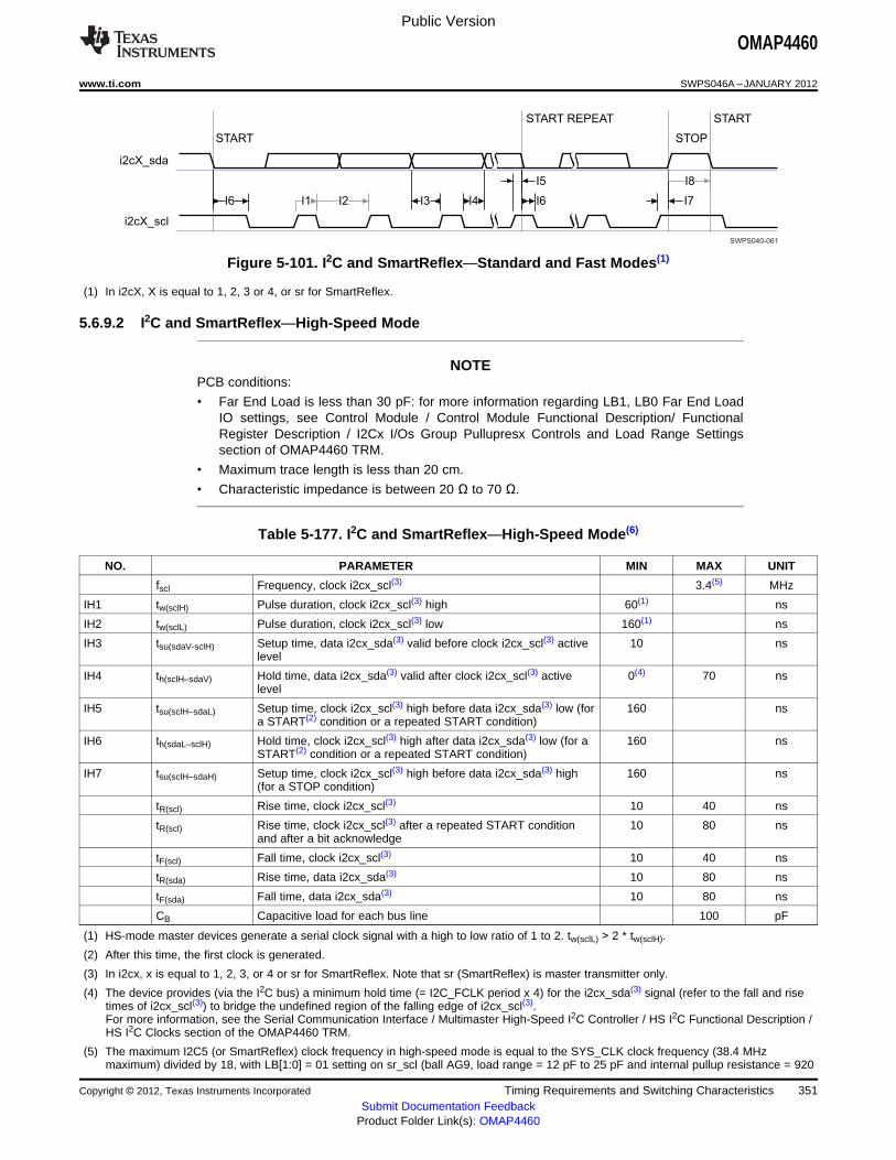
SWPS040-061
i2cX_sda
i2cX_scl
START REPEAT
STOPSTART
START
I1 I2 I3 I4
I5
I6I6 I7
I8
Public Version
OMAP4460
www.ti.com SWPS046A –JANUARY 2012
Figure 5-101. I2C and SmartReflex—Standard and Fast Modes(1)
(1) In i2cX, X is equal to 1, 2, 3 or 4, or sr for SmartReflex.
5.6.9.2 I2C and SmartReflex—High-Speed Mode
NOTEPCB conditions:
• Far End Load is less than 30 pF: for more information regarding LB1, LB0 Far End LoadIO settings, see Control Module / Control Module Functional Description/ FunctionalRegister Description / I2Cx I/Os Group Pullupresx Controls and Load Range Settingssection of OMAP4460 TRM.
• Maximum trace length is less than 20 cm.
• Characteristic impedance is between 20 Ω to 70 Ω.
Table 5-177. I2C and SmartReflex—High-Speed Mode(6)
NO. PARAMETER MIN MAX UNIT
fscl Frequency, clock i2cx_scl(3) 3.4(5) MHz
IH1 tw(sclH) Pulse duration, clock i2cx_scl(3) high 60(1) ns
IH2 tw(sclL) Pulse duration, clock i2cx_scl(3) low 160(1) ns
IH3 tsu(sdaV-sclH) Setup time, data i2cx_sda(3) valid before clock i2cx_scl(3) active 10 nslevel
IH4 th(sclH–sdaV) Hold time, data i2cx_sda(3) valid after clock i2cx_scl(3) active 0(4) 70 nslevel
IH5 tsu(sclH–sdaL) Setup time, clock i2cx_scl(3) high before data i2cx_sda(3) low (for 160 nsa START(2) condition or a repeated START condition)
IH6 th(sdaL–sclH) Hold time, clock i2cx_scl(3) high after data i2cx_sda(3) low (for a 160 nsSTART(2) condition or a repeated START condition)
IH7 tsu(sclH–sdaH) Setup time, clock i2cx_scl(3) high before data i2cx_sda(3) high 160 ns(for a STOP condition)
tR(scl) Rise time, clock i2cx_scl(3) 10 40 ns
tR(scl) Rise time, clock i2cx_scl(3) after a repeated START condition 10 80 nsand after a bit acknowledge
tF(scl) Fall time, clock i2cx_scl(3) 10 40 ns
tR(sda) Rise time, data i2cx_sda(3) 10 80 ns
tF(sda) Fall time, data i2cx_sda(3) 10 80 ns
CB Capacitive load for each bus line 100 pF
(1) HS-mode master devices generate a serial clock signal with a high to low ratio of 1 to 2. tw(sclL) > 2 * tw(sclH).
(2) After this time, the first clock is generated.
(3) In i2cx, x is equal to 1, 2, 3, or 4 or sr for SmartReflex. Note that sr (SmartReflex) is master transmitter only.
(4) The device provides (via the I2C bus) a minimum hold time (= I2C_FCLK period x 4) for the i2cx_sda(3) signal (refer to the fall and risetimes of i2cx_scl(3)) to bridge the undefined region of the falling edge of i2cx_scl(3).For more information, see the Serial Communication Interface / Multimaster High-Speed I2C Controller / HS I2C Functional Description /HS I2C Clocks section of the OMAP4460 TRM.
(5) The maximum I2C5 (or SmartReflex) clock frequency in high-speed mode is equal to the SYS_CLK clock frequency (38.4 MHzmaximum) divided by 18, with LB[1:0] = 01 setting on sr_scl (ball AG9, load range = 12 pF to 25 pF and internal pullup resistance = 920
Copyright © 2012, Texas Instruments Incorporated Timing Requirements and Switching Characteristics 351Submit Documentation Feedback
Product Folder Link(s): OMAP4460
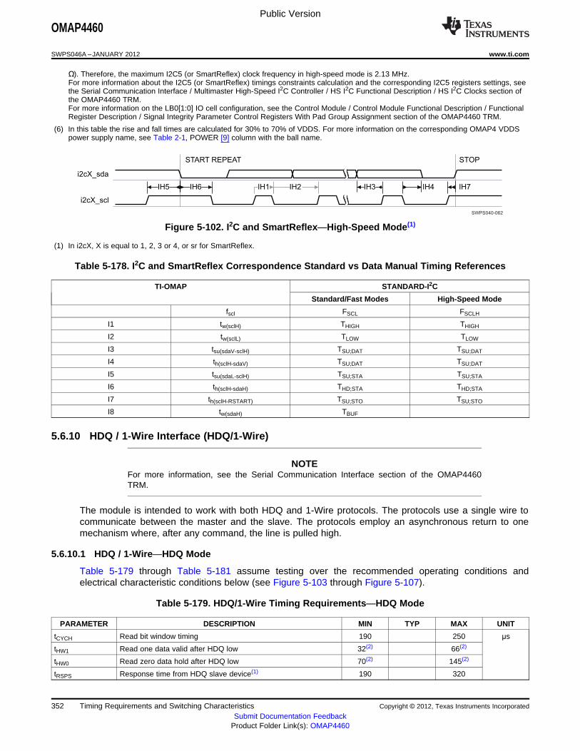
SWPS040-062
i2cX_sda
i2cX_scl
STOPSTART REPEAT
IH1 IH2 IH3 IH4IH6IH5 IH7
Public Version
OMAP4460
SWPS046A –JANUARY 2012 www.ti.com
Ω). Therefore, the maximum I2C5 (or SmartReflex) clock frequency in high-speed mode is 2.13 MHz.For more information about the I2C5 (or SmartReflex) timings constraints calculation and the corresponding I2C5 registers settings, seethe Serial Communication Interface / Multimaster High-Speed I2C Controller / HS I2C Functional Description / HS I2C Clocks section ofthe OMAP4460 TRM.For more information on the LB0[1:0] IO cell configuration, see the Control Module / Control Module Functional Description / FunctionalRegister Description / Signal Integrity Parameter Control Registers With Pad Group Assignment section of the OMAP4460 TRM.
(6) In this table the rise and fall times are calculated for 30% to 70% of VDDS. For more information on the corresponding OMAP4 VDDSpower supply name, see Table 2-1, POWER [9] column with the ball name.
Figure 5-102. I2C and SmartReflex—High-Speed Mode(1)
(1) In i2cX, X is equal to 1, 2, 3 or 4, or sr for SmartReflex.
Table 5-178. I2C and SmartReflex Correspondence Standard vs Data Manual Timing References
TI-OMAP STANDARD-I2C
Standard/Fast Modes High-Speed Mode
fscl FSCL FSCLH
I1 tw(sclH) THIGH THIGH
I2 tw(sclL) TLOW TLOW
I3 tsu(sdaV-sclH) TSU;DAT TSU;DAT
I4 th(sclH-sdaV) TSU;DAT TSU;DAT
I5 tsu(sdaL-sclH) TSU;STA TSU;STA
I6 th(sclH-sdaH) THD;STA THD;STA
I7 th(sclH-RSTART) TSU;STO TSU;STO
I8 tw(sdaH) TBUF
5.6.10 HDQ / 1-Wire Interface (HDQ/1-Wire)
NOTEFor more information, see the Serial Communication Interface section of the OMAP4460TRM.
The module is intended to work with both HDQ and 1-Wire protocols. The protocols use a single wire tocommunicate between the master and the slave. The protocols employ an asynchronous return to onemechanism where, after any command, the line is pulled high.
5.6.10.1 HDQ / 1-Wire—HDQ Mode
Table 5-179 through Table 5-181 assume testing over the recommended operating conditions andelectrical characteristic conditions below (see Figure 5-103 through Figure 5-107).
Table 5-179. HDQ/1-Wire Timing Requirements—HDQ Mode
PARAMETER DESCRIPTION MIN TYP MAX UNIT
tCYCH Read bit window timing 190 250 µs
tHW1 Read one data valid after HDQ low 32(2) 66(2)
tHW0 Read zero data hold after HDQ low 70(2) 145(2)
tRSPS Response time from HDQ slave device(1) 190 320
352 Timing Requirements and Switching Characteristics Copyright © 2012, Texas Instruments Incorporated
Submit Documentation FeedbackProduct Folder Link(s): OMAP4460
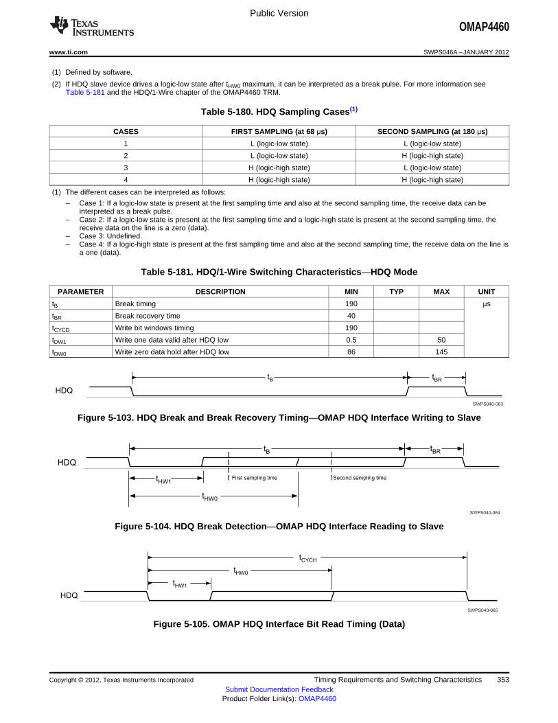
SWPS040-063
HDQ
tB t
BR
SWPS040-064
HDQ
tB tBR
tHW0
First sampling time Second sampling timetHW1
SWPS040-065
HDQ
tHW1
tHW0
tCYCH
Public Version
OMAP4460
www.ti.com SWPS046A –JANUARY 2012
(1) Defined by software.
(2) If HDQ slave device drives a logic-low state after tHW0 maximum, it can be interpreted as a break pulse. For more information seeTable 5-181 and the HDQ/1-Wire chapter of the OMAP4460 TRM.
Table 5-180. HDQ Sampling Cases(1)
CASES FIRST SAMPLING (at 68 µs) SECOND SAMPLING (at 180 µs)
1 L (logic-low state) L (logic-low state)
2 L (logic-low state) H (logic-high state)
3 H (logic-high state) L (logic-low state)
4 H (logic-high state) H (logic-high state)
(1) The different cases can be interpreted as follows:
– Case 1: If a logic-low state is present at the first sampling time and also at the second sampling time, the receive data can beinterpreted as a break pulse.
– Case 2: If a logic-low state is present at the first sampling time and a logic-high state is present at the second sampling time, thereceive data on the line is a zero (data).
– Case 3: Undefined.– Case 4: If a logic-high state is present at the first sampling time and also at the second sampling time, the receive data on the line is
a one (data).
Table 5-181. HDQ/1-Wire Switching Characteristics—HDQ Mode
PARAMETER DESCRIPTION MIN TYP MAX UNIT
tB Break timing 190 µs
tBR Break recovery time 40
tCYCD Write bit windows timing 190
tDW1 Write one data valid after HDQ low 0.5 50
tDW0 Write zero data hold after HDQ low 86 145
Figure 5-103. HDQ Break and Break Recovery Timing—OMAP HDQ Interface Writing to Slave
Figure 5-104. HDQ Break Detection—OMAP HDQ Interface Reading to Slave
Figure 5-105. OMAP HDQ Interface Bit Read Timing (Data)
Copyright © 2012, Texas Instruments Incorporated Timing Requirements and Switching Characteristics 353Submit Documentation Feedback
Product Folder Link(s): OMAP4460

SWPS040-066
HDQ
tDW1
tDW0
tCYCD
SWPS040-067
HDQ
Break
0_(LSB)
1 6 7_(MSB)
tRSPS 1
6
Command_byte_written Data_byte_received
0_(LSB)
SWPS040-068
1-WIRE
tRSTH
tPDLtPDHtRTSL
Public Version
OMAP4460
SWPS046A –JANUARY 2012 www.ti.com
Figure 5-106. OMAP HDQ Interface Bit Write Timing (Command / Address or Data)
Figure 5-107. HDQ Communication Timing
5.6.10.2 HDQ/1-Wire—1-Wire Mode
Table 5-182 and Table 5-183 assume testing over the recommended operating conditions and electricalcharacteristic conditions below (see Figure 5-108 through Figure 5-111).
Table 5-182. HDQ/1-Wire Timing Requirements—1-Wire Mode
PARAMETER DESCRIPTION MIN TYP MAX UNIT
tPDH Presence pulse delay high 15 60 µs
tPDL Presence pulse delay low 60 240
tRDV Read data valid time tLOWR 15
tREL Read data release time 0 45
Table 5-183. HDQ/1-Wire Switching Characteristics—1-Wire Mode
PARAMETER DESCRIPTION MIN TYP MAX UNIT
tRSTL Reset time low 480 960 µs
tRSTH Reset time high 480 µs
tSLOT Bit cycle time 60 120 µs
tLOW1 Write bit-one time 1 15 µs
tLOW0 Write bit-zero time(2) 60 120 µs
tREC Recovery time 1 µs
tLOWR Read bit strobe time(1) 1 15 µs
(1) tLOWR (low pulse sent by the master) must be short as possible to maximize the master sampling window.
(2) tLOW0 must be less than tSLOT.
Figure 5-108. 1-Wire—Break (Reset)
354 Timing Requirements and Switching Characteristics Copyright © 2012, Texas Instruments Incorporated
Submit Documentation FeedbackProduct Folder Link(s): OMAP4460
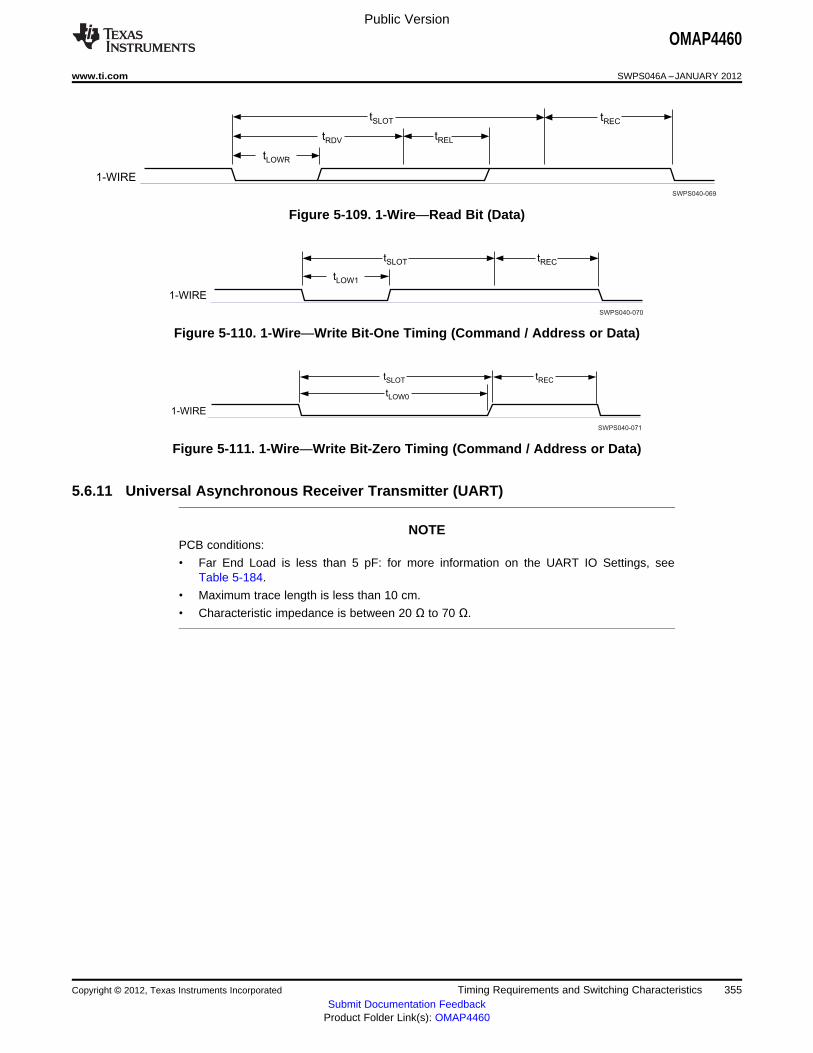
SWPS040-069
1-WIRE
tLOWR
tRDV
tSLOT
tREL
tREC
SWPS040-070
1-WIRE
tLOW1
tSLOT tREC
SWPS040-071
1-WIRE
tLOW0
tSLOT tREC
Public Version
OMAP4460
www.ti.com SWPS046A –JANUARY 2012
Figure 5-109. 1-Wire—Read Bit (Data)
Figure 5-110. 1-Wire—Write Bit-One Timing (Command / Address or Data)
Figure 5-111. 1-Wire—Write Bit-Zero Timing (Command / Address or Data)
5.6.11 Universal Asynchronous Receiver Transmitter (UART)
NOTEPCB conditions:
• Far End Load is less than 5 pF: for more information on the UART IO Settings, seeTable 5-184.
• Maximum trace length is less than 10 cm.
• Characteristic impedance is between 20 Ω to 70 Ω.
Copyright © 2012, Texas Instruments Incorporated Timing Requirements and Switching Characteristics 355Submit Documentation Feedback
Product Folder Link(s): OMAP4460

Public Version
OMAP4460
SWPS046A –JANUARY 2012 www.ti.com
Table 5-184. UART IO Settings References
MULTIPLEXING IO SETTINGS REFERENCESMODES IO SET 1 IO SET 2 IO SET 3 IO SET 4 IO SET 5 IO SET 6
UART1
Mode1 Balls: C26 / D26 Balls: AF23 / F27 Balls: AG23 /Signals: uart2_rx, Signals: uart1_rx, AH23uart1_tx uart1_tx Signals: uart1_cts,For more For more uart1_rtsinformation information For moreregarding LB[1:0] regarding LB[1:0] informationFar End Load IO and SC[1:0] Far regarding MB[1:0]settings, see End Load IO and LB0 Far EndControl Module / settings, see Load IO settings,Control Module Control Module / see ControlFunctional Control Module Module / ControlDescription/ Functional Module FunctionalFunctional Description/ Description/Register Functional FunctionalDescription / I2Cx Register RegisterI/Os Group Description / Description / 50-ΩPullupresx Low-Speed I/Os Output Buffer I/OsControls and Load Combined Slew With CombinedRange Settings Rate Versus TL Mode and Loadsection of Length and Load Settings section ofOMAP4460 TRM. Settings section of OMAP4460 TRM.
OMAP4460 TRM.
Mode2 Ball: E3 Ball: AA3Signal: uart1_rx Signal: uart1_rxFor more For moreinformation on informationSDMMC1_DR[2:0] regarding DS0 Far_SPEEDCTRL End Load IOregisters see: settings, seeControl Module / Control Module /Control Module Control ModuleFunctional FunctionalDescription / Description/Functional FunctionalRegister RegisterDescription / Description / I/OSignal Integrity Cells WithParameter Control ConfigurableRegisters With Output DriverPad Group Impedance sectionAssignment / of OMAP4460Device Interfaces TRM.Signal GroupControls Mappingsectionor,Control Module /Control ModuleRegister Manual /SYSCTRL_PADCONF_CORERegisterDescription sectionof the OMAP4460TRM.
UART2
356 Timing Requirements and Switching Characteristics Copyright © 2012, Texas Instruments Incorporated
Submit Documentation FeedbackProduct Folder Link(s): OMAP4460
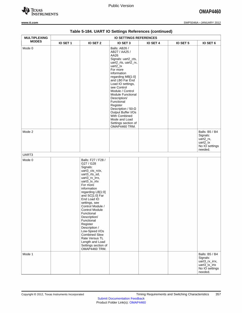
Public Version
OMAP4460
www.ti.com SWPS046A –JANUARY 2012
Table 5-184. UART IO Settings References (continued)
MULTIPLEXING IO SETTINGS REFERENCESMODES IO SET 1 IO SET 2 IO SET 3 IO SET 4 IO SET 5 IO SET 6
Mode 0 Balls: AB26 /AB27 / AA25 /AA26Signals: uart2_cts,uart2_rts, uart2_rx,uart2_txFor moreinformationregarding MB[1:0]and LB0 Far EndLoad IO settings,see ControlModule / ControlModule FunctionalDescription/FunctionalRegisterDescription / 50-ΩOutput Buffer I/OsWith CombinedMode and LoadSettings section ofOMAP4460 TRM.
Mode 2 Balls: B5 / B4Signals:uart2_rx,uart2_txNo IO settingsneeded.
UART3
Mode 0 Balls: F27 / F28 /G27 / G28Signals:uart3_cts_rctx,uart3_rts_sd,uart3_rx_irrx,uart3_tx_irtxFor moreinformationregarding LB[1:0]and SC[1:0] FarEnd Load IOsettings, seeControl Module /Control ModuleFunctionalDescription/FunctionalRegisterDescription /Low-Speed I/OsCombined SlewRate Versus TLLength and LoadSettings section ofOMAP4460 TRM.
Mode 1 Balls: B5 / B4Signals:uart3_rx_irrx,uart3_tx_irtxNo IO settingsneeded.
Copyright © 2012, Texas Instruments Incorporated Timing Requirements and Switching Characteristics 357Submit Documentation Feedback
Product Folder Link(s): OMAP4460

Public Version
OMAP4460
SWPS046A –JANUARY 2012 www.ti.com
Table 5-184. UART IO Settings References (continued)
MULTIPLEXING IO SETTINGS REFERENCESMODES IO SET 1 IO SET 2 IO SET 3 IO SET 4 IO SET 5 IO SET 6
Mode 2 Balls: W2 / W3 /W4 / Y2uart3_tx_irtx,uart3_rx_irrx,uart3_rts_sd,uart3_cts_rctxFor moreinformationregarding DS0 FarEnd Load IOsettings, seeControl Module /Control ModuleFunctionalDescription/FunctionalRegisterDescription / I/OCells WithConfigurableOutput DriverImpedance sectionof OMAP4460TRM.
UART4
Mode 0 Balls: AG20 /AH19uart4_rx, uart4_txFor moreinformationregarding MB[1:0]and LB0 Far EndLoad IO settings,see ControlModule / ControlModule FunctionalDescription/FunctionalRegisterDescription / 50-ΩOutput Buffer I/OsWith CombinedMode and LoadSettings section ofOMAP4460 TRM.
Mode 5 Balls: AE24 / AF24Signals: uart4_cts,uart4_rtsFor moreinformationregarding MB[1:0]and LB0 Far EndLoad IO settings,see ControlModule / ControlModule FunctionalDescription/FunctionalRegisterDescription / 50-ΩOutput Buffer I/OsWith CombinedMode and LoadSettings section ofOMAP4460 TRM.
358 Timing Requirements and Switching Characteristics Copyright © 2012, Texas Instruments Incorporated
Submit Documentation FeedbackProduct Folder Link(s): OMAP4460
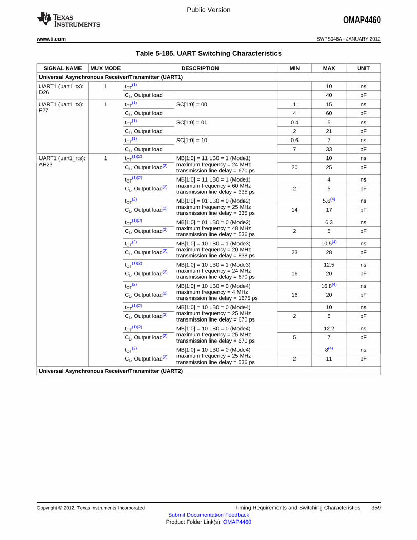
Public Version
OMAP4460
www.ti.com SWPS046A –JANUARY 2012
Table 5-185. UART Switching Characteristics
SIGNAL NAME MUX MODE DESCRIPTION MIN MAX UNIT
Universal Asynchronous Receiver/Transmitter (UART1)
UART1 (uart1_tx): 1 tOT(1) 10 ns
D26 CL, Output load 40 pF
UART1 (uart1_tx): 1 tOT(1) SC[1:0] = 00 1 15 ns
F27 CL, Output load 4 60 pF
tOT(1) SC[1:0] = 01 0.4 5 ns
CL, Output load 2 21 pF
tOT(1) SC[1:0] = 10 0.6 7 ns
CL, Output load 7 33 pF
UART1 (uart1_rts): 1 tOT(1)(2) MB[1:0] = 11 LB0 = 1 (Mode1) 10 ns
AH23 maximum frequency = 24 MHzCL, Output load(2) 20 25 pFtransmission line delay = 670 ps
tOT(1)(2) MB[1:0] = 11 LB0 = 1 (Mode1) 4 ns
maximum frequency = 60 MHzCL, Output load(2) 2 5 pFtransmission line delay = 335 ps
tOT(2) MB[1:0] = 01 LB0 = 0 (Mode2) 5.6(4) ns
maximum frequency = 25 MHzCL, Output load(2) 14 17 pFtransmission line delay = 335 ps
tOT(1)(2) MB[1:0] = 01 LB0 = 0 (Mode2) 6.3 ns
maximum frequency = 48 MHzCL, Output load(2) 2 5 pFtransmission line delay = 536 ps
tOT(2) MB[1:0] = 10 LB0 = 1 (Mode3) 10.5(4) ns
maximum frequency = 20 MHzCL, Output load(2) 23 28 pFtransmission line delay = 838 ps
tOT(1)(2) MB[1:0] = 10 LB0 = 1 (Mode3) 12.5 ns
maximum frequency = 24 MHzCL, Output load(2) 16 20 pFtransmission line delay = 670 ps
tOT(2) MB[1:0] = 10 LB0 = 0 (Mode4) 16.8(4) ns
maximum frequency = 4 MHzCL, Output load(2) 16 20 pFtransmission line delay = 1675 ps
tOT(1)(2) MB[1:0] = 10 LB0 = 0 (Mode4) 10 ns
maximum frequency = 25 MHzCL, Output load(2) 2 5 pFtransmission line delay = 670 ps
tOT(1)(2) MB[1:0] = 10 LB0 = 0 (Mode4) 12.2 ns
maximum frequency = 25 MHzCL, Output load(2) 5 7 pFtransmission line delay = 670 ps
tOT(2) MB[1:0] = 10 LB0 = 0 (Mode4) 8(4) ns
maximum frequency = 25 MHzCL, Output load(2) 2 11 pFtransmission line delay = 536 ps
Universal Asynchronous Receiver/Transmitter (UART2)
Copyright © 2012, Texas Instruments Incorporated Timing Requirements and Switching Characteristics 359Submit Documentation Feedback
Product Folder Link(s): OMAP4460

Public Version
OMAP4460
SWPS046A –JANUARY 2012 www.ti.com
Table 5-185. UART Switching Characteristics (continued)
SIGNAL NAME MUX MODE DESCRIPTION MIN MAX UNIT
UART2 (uart2_rts, 0 tOT(1)(2) MB[1:0] = 11 LB0 = 1 (Mode1) 10 ns
uart2_tx): AB27 / maximum frequency = 24 MHzCL, Output load 20 25 pFAA26 transmission line delay = 670 ps
tOT(1)(2) MB[1:0] = 11 LB0 = 1 (Mode1) 4 ns
maximum frequency = 60 MHzCL, Output load 2 5 pFtransmission line delay = 335 ps
tOT(2) MB[1:0] = 01 LB0 = 0 (Mode2) 5.6(4) ns
maximum frequency = 25 MHzCL, Output load 14 17 pFtransmission line delay = 335 ps
tOT(1)(2) MB[1:0] = 01 LB0 = 0 (Mode2) 6.3 ns
maximum frequency = 48 MHzCL, Output load 2 5 pFtransmission line delay = 536 ps
tOT(2) MB[1:0] = 10 LB0 = 1 (Mode3) 10.5(4) ns
maximum frequency = 20 MHzCL, Output load 23 28 pFtransmission line delay = 838 ps
tOT(1)(2) MB[1:0] = 10 LB0 = 1 (Mode3) 12.5 ns
maximum frequency = 24 MHzCL, Output load 16 20 pFtransmission line delay = 670 ps
tOT(2) MB[1:0] = 10 LB0 = 0 (Mode4) 16.8(4) ns
maximum frequency = 4 MHzCL, Output load 16 20 pFtransmission line delay = 1675 ps
tOT(1)(2) MB[1:0] = 10 LB0 = 0 (Mode4) 10 ns
maximum frequency = 25 MHzCL, Output load 2 5 pFtransmission line delay = 670 ps
tOT(1)(2) MB[1:0] = 10 LB0 = 0 (Mode4) 12.2 ns
maximum frequency = 25 MHzCL, Output load 5 7 pFtransmission line delay = 670 ps
tOT(2) MB[1:0] = 10 LB0 = 0 (Mode4) 8(4) ns
maximum frequency = 25 MHzCL, Output load 2 11 pFtransmission line delay = 536 ps
UART2 (uart2_rx, 2 tOT(1) 4 30 ns
uart2_tx) : B5 / B4 CL, Output load 0 50 pF
Universal Asynchronous Receiver/Transmitter (UART3)
UART3 0 tOT(1) SC[1:0] = 00 1 15 ns
(uart3_cts_rctx, CL, Output load 4 60 pFuart3_rts_sd,
tOT(1) SC[1:0] = 01 0.4 5 nsuart3_tx_irtx): F27
/ F28 / G28 CL, Output load 2 21 pF
tOT(1) SC[1:0] = 10 0.6 7 ns
CL, Output load 7 33 pF
UART3 1 tOT(1) 4 30 ns
(uart3_rx_irrx, CL, Output load 0 50 pFuart3_tx_irtx): B5 /B4
UART3 2 tOT DS0 = 0 (Mode2) 15(3) ns(uart3_tx_irtx, maximum frequency = 20 MHzCL, Output load 5 35 pFuart3_rts_sd, transmission line delay = 1340 psuart3_cts_rctx): W2 tOT DS0 = 0 (Mode2) 3(3) ns/ W4 / Y2 maximum frequency = 48 MHzCL, Output load 2 5 pF
transmission line delay = 670 ps
tOT DS0 = 0 (Mode2) 3(4) nsmaximum frequency = 60 MHzCL, Output load 2 5 pFtransmission line delay = 335 ps
tOT DS0 = 0 (Mode2) 4(1) nsmaximum frequency = 75 MHzCL, Output load 2 5 pFtransmission line delay = 402 ps
tOT DS0 = 1 (Mode1) 2(1) nsmaximum frequency = 100 MHzCL, Output load 2 5 pFtransmission line delay = 203 ps
360 Timing Requirements and Switching Characteristics Copyright © 2012, Texas Instruments Incorporated
Submit Documentation FeedbackProduct Folder Link(s): OMAP4460
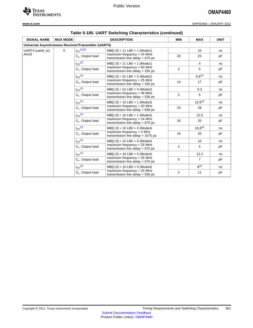
Public Version
OMAP4460
www.ti.com SWPS046A –JANUARY 2012
Table 5-185. UART Switching Characteristics (continued)
SIGNAL NAME MUX MODE DESCRIPTION MIN MAX UNIT
Universal Asynchronous Receiver/Transmitter (UART4)
UART4 (uart4_tx): 0 tOT(1)(2) MB[1:0] = 11 LB0 = 1 (Mode1) 10 ns
AH19 maximum frequency = 24 MHzCL, Output load 20 25 pFtransmission line delay = 670 ps
tOT(2) MB[1:0] = 11 LB0 = 1 (Mode1) 4 ns
maximum frequency = 60 MHzCL, Output load 2 5 pFtransmission line delay = 335 ps
tOT(2) MB[1:0] = 01 LB0 = 0 (Mode2) 5.6(4) ns
maximum frequency = 25 MHzCL, Output load 14 17 pFtransmission line delay = 335 ps
tOT(2) MB[1:0] = 01 LB0 = 0 (Mode2) 6.3 ns
maximum frequency = 48 MHzCL, Output load 2 5 pFtransmission line delay = 536 ps
tOT(2) MB[1:0] = 10 LB0 = 1 (Mode3) 10.5(4) ns
maximum frequency = 20 MHzCL, Output load 23 28 pFtransmission line delay = 838 ps
tOT(2) MB[1:0] = 10 LB0 = 1 (Mode3) 12.5 ns
maximum frequency = 24 MHzCL, Output load 16 20 pFtransmission line delay = 670 ps
tOT(2) MB[1:0] = 10 LB0 = 0 (Mode4) 16.8(4) ns
maximum frequency = 4 MHzCL, Output load 16 20 pFtransmission line delay = 1675 ps
tOT(2) MB[1:0] = 10 LB0 = 0 (Mode4) 10 ns
maximum frequency = 25 MHzCL, Output load 2 5 pFtransmission line delay = 670 ps
tOT(2) MB[1:0] = 10 LB0 = 0 (Mode4) 12.2 ns
maximum frequency = 25 MHzCL, Output load 5 7 pFtransmission line delay = 670 ps
tOT(2) MB[1:0] = 10 LB0 = 0 (Mode4) 8(4) ns
maximum frequency = 25 MHzCL, Output load 2 11 pFtransmission line delay = 536 ps
Copyright © 2012, Texas Instruments Incorporated Timing Requirements and Switching Characteristics 361Submit Documentation Feedback
Product Folder Link(s): OMAP4460
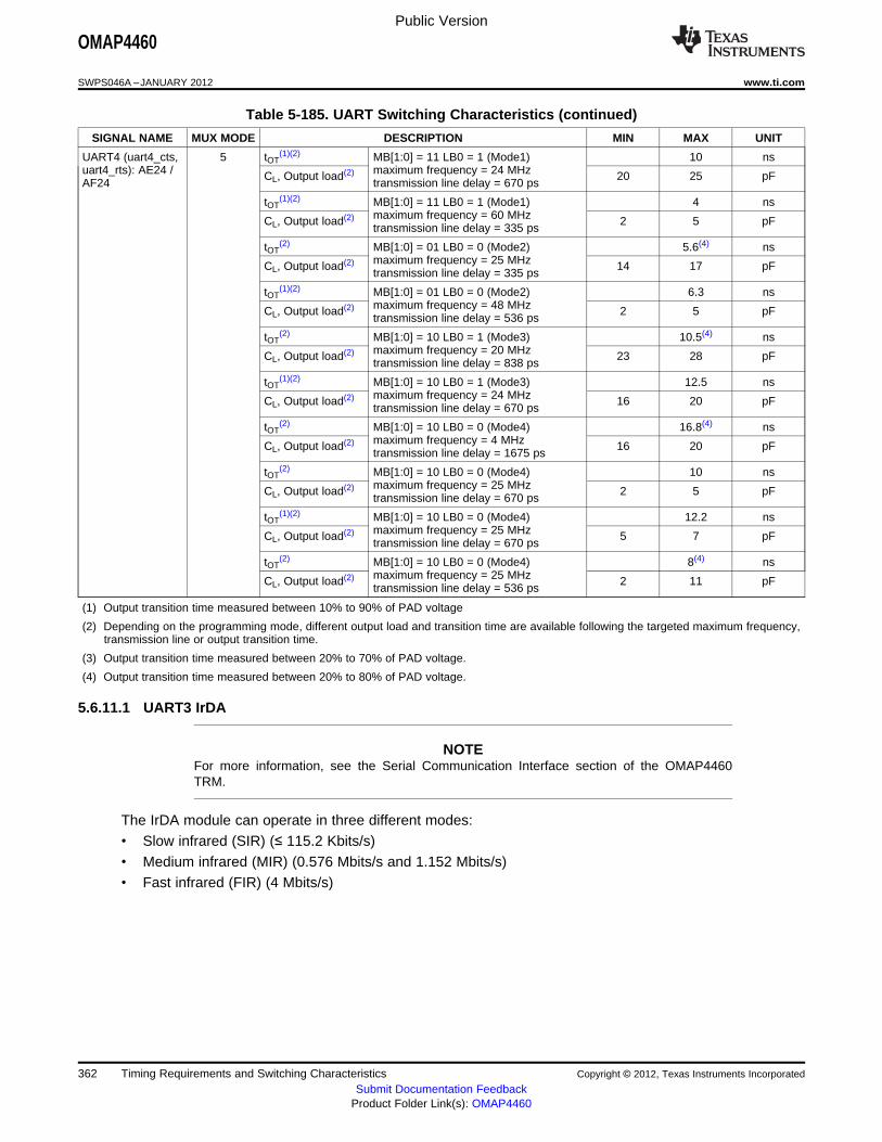
Public Version
OMAP4460
SWPS046A –JANUARY 2012 www.ti.com
Table 5-185. UART Switching Characteristics (continued)
SIGNAL NAME MUX MODE DESCRIPTION MIN MAX UNIT
UART4 (uart4_cts, 5 tOT(1)(2) MB[1:0] = 11 LB0 = 1 (Mode1) 10 ns
uart4_rts): AE24 / maximum frequency = 24 MHzCL, Output load(2) 20 25 pFAF24 transmission line delay = 670 ps
tOT(1)(2) MB[1:0] = 11 LB0 = 1 (Mode1) 4 ns
maximum frequency = 60 MHzCL, Output load(2) 2 5 pFtransmission line delay = 335 ps
tOT(2) MB[1:0] = 01 LB0 = 0 (Mode2) 5.6(4) ns
maximum frequency = 25 MHzCL, Output load(2) 14 17 pFtransmission line delay = 335 ps
tOT(1)(2) MB[1:0] = 01 LB0 = 0 (Mode2) 6.3 ns
maximum frequency = 48 MHzCL, Output load(2) 2 5 pFtransmission line delay = 536 ps
tOT(2) MB[1:0] = 10 LB0 = 1 (Mode3) 10.5(4) ns
maximum frequency = 20 MHzCL, Output load(2) 23 28 pFtransmission line delay = 838 ps
tOT(1)(2) MB[1:0] = 10 LB0 = 1 (Mode3) 12.5 ns
maximum frequency = 24 MHzCL, Output load(2) 16 20 pFtransmission line delay = 670 ps
tOT(2) MB[1:0] = 10 LB0 = 0 (Mode4) 16.8(4) ns
maximum frequency = 4 MHzCL, Output load(2) 16 20 pFtransmission line delay = 1675 ps
tOT(2) MB[1:0] = 10 LB0 = 0 (Mode4) 10 ns
maximum frequency = 25 MHzCL, Output load(2) 2 5 pFtransmission line delay = 670 ps
tOT(1)(2) MB[1:0] = 10 LB0 = 0 (Mode4) 12.2 ns
maximum frequency = 25 MHzCL, Output load(2) 5 7 pFtransmission line delay = 670 ps
tOT(2) MB[1:0] = 10 LB0 = 0 (Mode4) 8(4) ns
maximum frequency = 25 MHzCL, Output load(2) 2 11 pFtransmission line delay = 536 ps
(1) Output transition time measured between 10% to 90% of PAD voltage
(2) Depending on the programming mode, different output load and transition time are available following the targeted maximum frequency,transmission line or output transition time.
(3) Output transition time measured between 20% to 70% of PAD voltage.
(4) Output transition time measured between 20% to 80% of PAD voltage.
5.6.11.1 UART3 IrDA
NOTEFor more information, see the Serial Communication Interface section of the OMAP4460TRM.
The IrDA module can operate in three different modes:• Slow infrared (SIR) (≤ 115.2 Kbits/s)• Medium infrared (MIR) (0.576 Mbits/s and 1.152 Mbits/s)• Fast infrared (FIR) (4 Mbits/s)
362 Timing Requirements and Switching Characteristics Copyright © 2012, Texas Instruments Incorporated
Submit Documentation FeedbackProduct Folder Link(s): OMAP4460
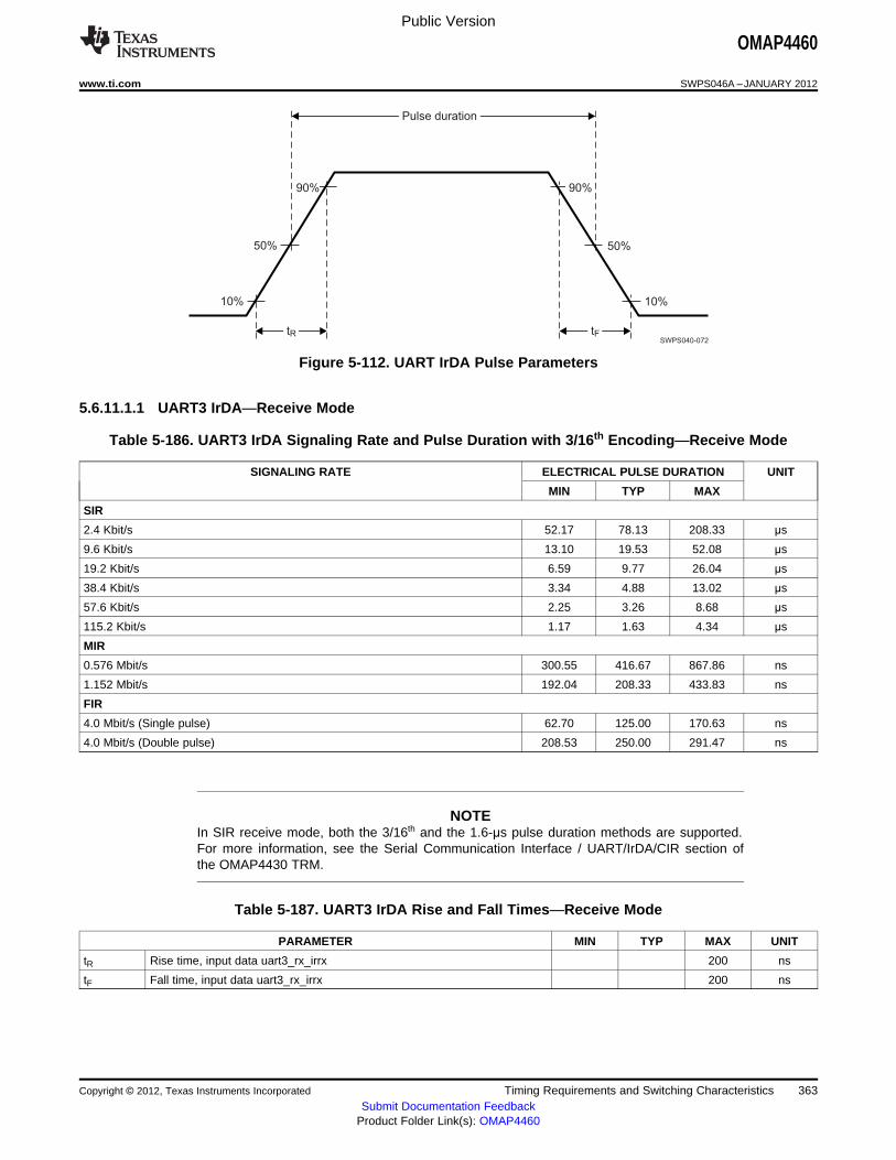
SWPS040-072
Pulse duration
90% 90%
50% 50%
10% 10%
tR tF
Public Version
OMAP4460
www.ti.com SWPS046A –JANUARY 2012
Figure 5-112. UART IrDA Pulse Parameters
5.6.11.1.1 UART3 IrDA—Receive Mode
Table 5-186. UART3 IrDA Signaling Rate and Pulse Duration with 3/16th Encoding—Receive Mode
SIGNALING RATE ELECTRICAL PULSE DURATION UNIT
MIN TYP MAX
SIR
2.4 Kbit/s 52.17 78.13 208.33 µs
9.6 Kbit/s 13.10 19.53 52.08 µs
19.2 Kbit/s 6.59 9.77 26.04 µs
38.4 Kbit/s 3.34 4.88 13.02 µs
57.6 Kbit/s 2.25 3.26 8.68 µs
115.2 Kbit/s 1.17 1.63 4.34 µs
MIR
0.576 Mbit/s 300.55 416.67 867.86 ns
1.152 Mbit/s 192.04 208.33 433.83 ns
FIR
4.0 Mbit/s (Single pulse) 62.70 125.00 170.63 ns
4.0 Mbit/s (Double pulse) 208.53 250.00 291.47 ns
space
NOTEIn SIR receive mode, both the 3/16th and the 1.6-μs pulse duration methods are supported.For more information, see the Serial Communication Interface / UART/IrDA/CIR section ofthe OMAP4430 TRM.
Table 5-187. UART3 IrDA Rise and Fall Times—Receive Mode
PARAMETER MIN TYP MAX UNIT
tR Rise time, input data uart3_rx_irrx 200 ns
tF Fall time, input data uart3_rx_irrx 200 ns
Copyright © 2012, Texas Instruments Incorporated Timing Requirements and Switching Characteristics 363Submit Documentation Feedback
Product Folder Link(s): OMAP4460
Public Version
OMAP4460
SWPS046A –JANUARY 2012 www.ti.com
5.6.11.1.2 UART3 IrDA—Transmit Mode
Table 5-188. UART3 IrDA Signaling Rate and Pulse Duration with 3/16th Encoding—Transmit Mode
SIGNALING RATE ELECTRICAL PULSE DURATION UNIT
MIN TYP MAX
SIR
2.4 Kbit/s 78.1 78.1 78.1 µs
9.6 Kbit/s 19.5 19.5 19.5 µs
19.2 Kbit/s 9.75 9.75 9.75 µs
38.4 Kbit/s 4.87 4.87 4.87 µs
57.6 Kbit/s 3.25 3.25 3.25 µs
115.2 Kbit/s 1.62 1.62 1.62 µs
MIR
0.576 Mbit/s 414 416 419 ns
1.152 Mbit/s 206 208 211 ns
FIR
4.0 Mbit/s (Single pulse) 123 125 128 ns
4.0 Mbit/s (Double pulse) 248 250 253 ns
space
NOTEIn SIR transmit mode, both the 3/16th and the 1.6-μs pulse duration methods are supported.For more information, see the Serial Communication Interface / UART/IrDA/CIR section ofthe OMAP4430 TRM.
364 Timing Requirements and Switching Characteristics Copyright © 2012, Texas Instruments Incorporated
Submit Documentation FeedbackProduct Folder Link(s): OMAP4460

Public Version
OMAP4460
www.ti.com SWPS046A –JANUARY 2012
5.7 Removable Media Interfaces
NOTEFor more information, see the MMC/SD/SDIO section of the OMAP4460 TRM.
The MMC/SD/SDIO host controller provides an interface to MMC, SD memory cards or SDIO cards. TheMMC/SD/SDIO host controller deals with MMC/SD/SDIO protocol at transmission level, data packing,adding cyclic redundancy checks (CRC), start/end bit, and checking for syntactical correctness.
There are five MMC/SD/SDIO host controllers inside the device:• MMC/SD/SDIO1:
– 1.8-V / 3-V support– 1-bit, 4-bit, and 8-bit data transfers without external transceiver
• MMC/SD/SDIO2:– Only 1.8-V support– 1-bit, 4-bit, and 8-bit data transfers without external transceiver– 8-bit with external transceiver allowing supporting 3-V peripherals
• MMC/SD/SDIO3, MMC/SD/SDIO4, and MMC/SD/SDIO5:– Only 1.8-V support– 1-bit and 4-bit data transfers without external transceiver
5.7.1 Multimedia Memory Card and Secure Digital IO Card (SDMMC)
5.7.1.1 MMC/SD/SDIO 1 Interface
5.7.1.1.1 MMC/SD/SDIO 1 Interface—SD Identification and Standard SD Mode
Table 5-190 and Table 5-191 assume testing over the recommended operating conditions and electricalcharacteristic conditions below (see Figure 5-113 and Figure 5-114).
Table 5-189. MMC/SD/SDIO 1 Interface Timing Conditions—SD Identification and Standard SDMode(1)(2)(3)(4)
TIMING CONDITION PARAMETER VALUE UNIT
MIN MAX
Input Conditions
tR Input signal rise time 10 ns
tF Input signal fall time 10 ns
PCB Conditions
Number of external peripherals 1
Far end load 40 pF
Trace length for SD car types 10 cm
Characteristics impedance SanDisk Extreme III cards 45 55 ΩOther card types 20 70
(1) IO settings: SPEEDCTRL = 0For more information, see
– The Control Module Functional Description / Extended-Drain I/O and PBIAS Cell / Extended-Drain I/O section or– The Control Module / Control Module Functional Description / Functional Register Description / Signal Integrity Parameter Control
Registers with Pad Group Assignment / Device Interfaces Signal Group Controls Mapping sectionof the OMAP4460 TRM.
(2) In this table the rise and fall times are calculated for the VIL / VIH described in Section 3.3.11, MMC/SDIO DC Electrical Characteristics.
(3) For more information on SDMMC ESD guideline examples, see Section A.3.2.2.1, ESD Implementation—MMC/SD/SDIO 1Interface—SD Mode.
(4) To have an idea of the output OMAP4 ball load supported for this application, you can consider the following:
Copyright © 2012, Texas Instruments Incorporated Timing Requirements and Switching Characteristics 365Submit Documentation Feedback
Product Folder Link(s): OMAP4460
Public Version
OMAP4460
SWPS046A –JANUARY 2012 www.ti.com
Output OMAP4 ball load = Far End load + 1.34 pF/cm typical x trace length (cm).
Table 5-190. MMC/SD/SDIO 1 Interface Timing Requirements—SD Identification and Standard SDMode(1)(2)
NO. PARAMETER OPP100, OPP119 OPP50 UNIT
MIN MAX MIN MAX
SD Identification Mode
SD3 tsu(CMDV-CLKH) Setup time, sdmmc1_cmd valid before 1198.2 1198.2 nssdmmc1_clk rising clock edge
SD4 th(clkH-CMDIV) Hold time, sdmmc1_cmd valid after 1249.0 1249.0 nssdmmc1_clk rising clock edge
MMC/SD/SDIO 1 Interface (1.8-V IO) Standard SD Mode
SD3 tsu(CMDV-CLKH) Setup time, sdmmc1_cmd valid before 6.0 6.0 nssdmmc1_clk rising clock edge
SD4 th(clkH-CMDIV) Hold time, sdmmc1_cmd valid after 19.2 19.2 nssdmmc1_clk rising clock edge
SD7 tsu(datV-CLKH) Setup time, sdmmc1_dat[n:0] valid before 6.0 6.0 nssdmmc1_clk rising clock edge
SD8 th(clkH-datIV) Hold time, sdmmc1_dat[n:0] valid after 19.2 19.2 nssdmmc1_clk rising clock edge
MMC/SD/SDIO 1 Interface (3.3-V IO) Standard SD Mode
SD3 tsu(CMDV-CLKH) Setup time, sdmmc1_cmd valid before 6.0 6.0 nssdmmc1_clk rising clock edge
SD4 th(clkH-CMDIV) Hold time, sdmmc1_cmd valid after 19.2 19.2 nssdmmc1_clk rising clock edge
SD7 tsu(datV-CLKH) Setup time, sdmmc1_dat[n:0] valid before 6.0 6.0 nssdmmc1_clk rising clock edge
SD8 th(clkH-datIV) Hold time, sdmmc1_dat[n:0] valid after 19.2 19.2 nssdmmc1_clk rising clock edge
(1) In sdmmc1_dat[n:0], n up to 7
(2) See DM Operating Condition Addendum for CORE OPP voltages.
Table 5-191. MMC/SD/SDIO 1 Interface Switching Characteristics—SD Identification and Standard SDMode(1)(3)(4)
NO. PARAMETER OPP100, OPP119 OPP50 UNIT
MIN MAX MIN MAX
SD Identification Mode
SD1 1 / tclk Frequency, sdmmc1_clk 0.4 0.4 MHz
SD2 tw(clk) Pulse duration, sdmmc1_clk high or low 0.45*P(2) 0.55*P(2) 0.45*P(2) 0.55*P(2) ns
SD5 td(clkH-CMDT) Delay time, sdmmc1_clk rising clock edge to 6.5 2492.5 6.5 2492.5 nssdmmc1_cmd transition
MMC/SD/SDIO 1 Interface (1.8-V IO) Standard SD Mode
SD1 1 / tclk Frequency, sdmmc1_clk 24 24 MHz
SD2 tw(clk) Pulse duration, sdmmc1_clk high or low 0.45*P(2) 0.55*P(2) 0.45*P(2) 0.55*P(2) ns
SD5 td(clkH-CMD) Delay time, sdmmc1_clk rising clock edge to 6.3 35.3 6.3 35.3 nssdmmc1_cmd transition
SD6 td(clkH-dat) Delay time, sdmmc1_clk rising clock edge to 6.3 35.3 6.3 35.3 nssdmmc1_dat[n:0] transition
MMC/SD/SDIO 1 Interface (3.3-V IO) Standard SD Mode
SD1 1 / tclk Frequency, sdmmc1_clk 24 24 MHz
SD2 tw(clk) Pulse duration, sdmmc1_clk high or low 0.45*P(2) 0.55*P(2) 0.45*P(2) 0.55*P(2) ns
SD5 td(clkH-CMD) Delay time, sdmmc1_clk rising clock edge to 6.3 35.3 6.3 35.3 nssdmmc1_cmd transition
366 Timing Requirements and Switching Characteristics Copyright © 2012, Texas Instruments Incorporated
Submit Documentation FeedbackProduct Folder Link(s): OMAP4460
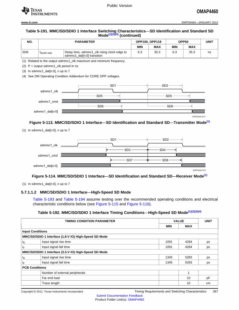
SWPS040-073
sdmmc1_clk
SD5
SD6
SD5
SD6
SD1 SD2
sdmmc1_cmd
sdmmc1_dat[n:0]
SWPS040-074
sdmmc1_clk
sdmmc1_cmd
sdmmc1_dat[n:0]
SD4
SD8
SD3
SD7
SD1 SD2
Public Version
OMAP4460
www.ti.com SWPS046A –JANUARY 2012
Table 5-191. MMC/SD/SDIO 1 Interface Switching Characteristics—SD Identification and Standard SDMode(1)(3)(4) (continued)
NO. PARAMETER OPP100, OPP119 OPP50 UNIT
MIN MAX MIN MAX
SD6 td(clkH-dat) Delay time, sdmmc1_clk rising clock edge to 6.3 35.3 6.3 35.3 nssdmmc1_dat[n:0] transition
(1) Related to the output sdmmc1_clk maximum and minimum frequency.
(2) P = output sdmmc1_clk period in ns
(3) In sdmmc1_dat[n:0], n up to 7
(4) See DM Operating Condition Addendum for CORE OPP voltages.
Figure 5-113. MMC/SD/SDIO 1 Interface—SD Identification and Standard SD—Transmitter Mode(1)
(1) In sdmmc1_dat[n:0], n up to 7
Figure 5-114. MMC/SD/SDIO 1 Interface—SD Identification and Standard SD—Receiver Mode(1)
(1) In sdmmc1_dat[n:0], n up to 7
5.7.1.1.2 MMC/SD/SDIO 1 Interface—High-Speed SD Mode
Table 5-193 and Table 5-194 assume testing over the recommended operating conditions and electricalcharacteristic conditions below (see Figure 5-115 and Figure 5-116).
Table 5-192. MMC/SD/SDIO 1 Interface Timing Conditions—High-Speed SD Mode(1)(2)(3)(4)
TIMING CONDITION PARAMETER VALUE UNIT
MIN MAX
Input Conditions
MMC/SD/SDIO 1 Interface (1.8-V IO) High-Speed SD Mode
tR Input signal rise time 1091 4284 ps
tF Input signal fall time 1091 4284 ps
MMC/SD/SDIO 1 Interface (3.3-V IO) High-Speed SD Mode
tR Input signal rise time 1345 5283 ps
tF Input signal fall time 1345 5283 ps
PCB Conditions
Number of external peripherals 1
Far end load 10 pF
Trace length 10 cm
Copyright © 2012, Texas Instruments Incorporated Timing Requirements and Switching Characteristics 367Submit Documentation Feedback
Product Folder Link(s): OMAP4460
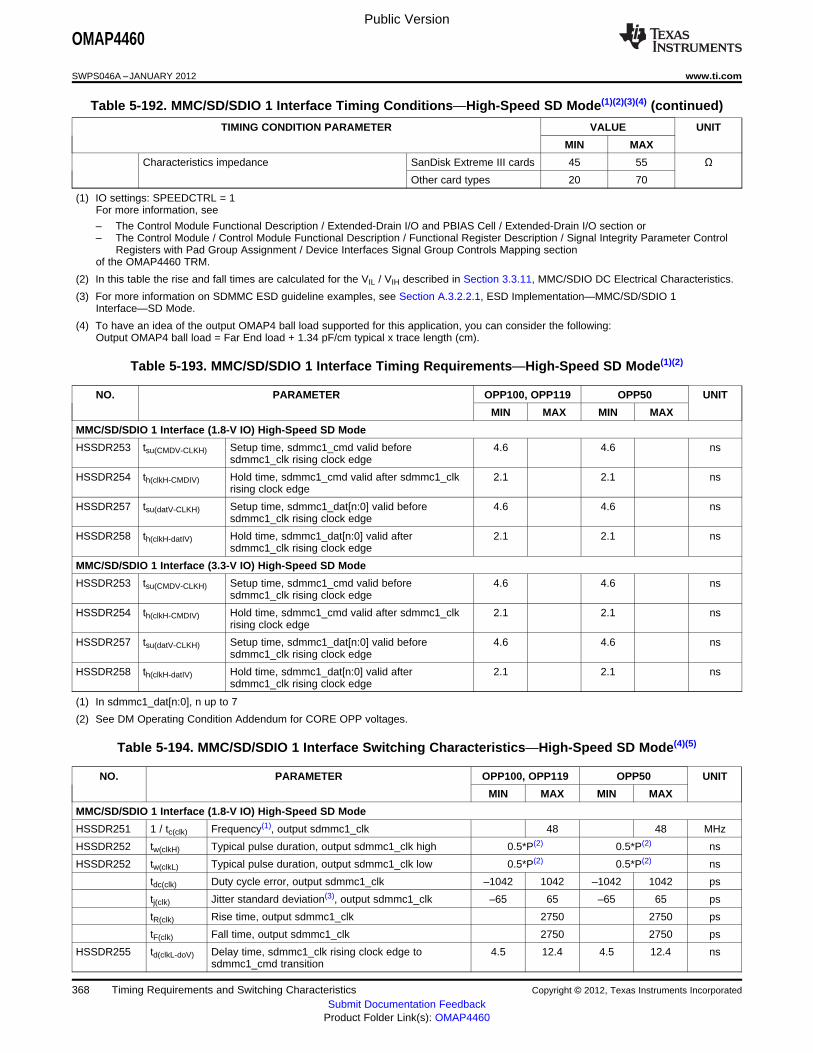
Public Version
OMAP4460
SWPS046A –JANUARY 2012 www.ti.com
Table 5-192. MMC/SD/SDIO 1 Interface Timing Conditions—High-Speed SD Mode(1)(2)(3)(4) (continued)
TIMING CONDITION PARAMETER VALUE UNIT
MIN MAX
Characteristics impedance SanDisk Extreme III cards 45 55 ΩOther card types 20 70
(1) IO settings: SPEEDCTRL = 1For more information, see
– The Control Module Functional Description / Extended-Drain I/O and PBIAS Cell / Extended-Drain I/O section or– The Control Module / Control Module Functional Description / Functional Register Description / Signal Integrity Parameter Control
Registers with Pad Group Assignment / Device Interfaces Signal Group Controls Mapping sectionof the OMAP4460 TRM.
(2) In this table the rise and fall times are calculated for the VIL / VIH described in Section 3.3.11, MMC/SDIO DC Electrical Characteristics.
(3) For more information on SDMMC ESD guideline examples, see Section A.3.2.2.1, ESD Implementation—MMC/SD/SDIO 1Interface—SD Mode.
(4) To have an idea of the output OMAP4 ball load supported for this application, you can consider the following:Output OMAP4 ball load = Far End load + 1.34 pF/cm typical x trace length (cm).
Table 5-193. MMC/SD/SDIO 1 Interface Timing Requirements—High-Speed SD Mode(1)(2)
NO. PARAMETER OPP100, OPP119 OPP50 UNIT
MIN MAX MIN MAX
MMC/SD/SDIO 1 Interface (1.8-V IO) High-Speed SD Mode
HSSDR253 tsu(CMDV-CLKH) Setup time, sdmmc1_cmd valid before 4.6 4.6 nssdmmc1_clk rising clock edge
HSSDR254 th(clkH-CMDIV) Hold time, sdmmc1_cmd valid after sdmmc1_clk 2.1 2.1 nsrising clock edge
HSSDR257 tsu(datV-CLKH) Setup time, sdmmc1_dat[n:0] valid before 4.6 4.6 nssdmmc1_clk rising clock edge
HSSDR258 th(clkH-datIV) Hold time, sdmmc1_dat[n:0] valid after 2.1 2.1 nssdmmc1_clk rising clock edge
MMC/SD/SDIO 1 Interface (3.3-V IO) High-Speed SD Mode
HSSDR253 tsu(CMDV-CLKH) Setup time, sdmmc1_cmd valid before 4.6 4.6 nssdmmc1_clk rising clock edge
HSSDR254 th(clkH-CMDIV) Hold time, sdmmc1_cmd valid after sdmmc1_clk 2.1 2.1 nsrising clock edge
HSSDR257 tsu(datV-CLKH) Setup time, sdmmc1_dat[n:0] valid before 4.6 4.6 nssdmmc1_clk rising clock edge
HSSDR258 th(clkH-datIV) Hold time, sdmmc1_dat[n:0] valid after 2.1 2.1 nssdmmc1_clk rising clock edge
(1) In sdmmc1_dat[n:0], n up to 7
(2) See DM Operating Condition Addendum for CORE OPP voltages.
Table 5-194. MMC/SD/SDIO 1 Interface Switching Characteristics—High-Speed SD Mode(4)(5)
NO. PARAMETER OPP100, OPP119 OPP50 UNIT
MIN MAX MIN MAX
MMC/SD/SDIO 1 Interface (1.8-V IO) High-Speed SD Mode
HSSDR251 1 / tc(clk) Frequency(1), output sdmmc1_clk 48 48 MHz
HSSDR252 tw(clkH) Typical pulse duration, output sdmmc1_clk high 0.5*P(2) 0.5*P(2) ns
HSSDR252 tw(clkL) Typical pulse duration, output sdmmc1_clk low 0.5*P(2) 0.5*P(2) ns
tdc(clk) Duty cycle error, output sdmmc1_clk –1042 1042 –1042 1042 ps
tj(clk) Jitter standard deviation(3), output sdmmc1_clk –65 65 –65 65 ps
tR(clk) Rise time, output sdmmc1_clk 2750 2750 ps
tF(clk) Fall time, output sdmmc1_clk 2750 2750 ps
HSSDR255 td(clkL-doV) Delay time, sdmmc1_clk rising clock edge to 4.5 12.4 4.5 12.4 nssdmmc1_cmd transition
368 Timing Requirements and Switching Characteristics Copyright © 2012, Texas Instruments Incorporated
Submit Documentation FeedbackProduct Folder Link(s): OMAP4460

SWPS040-075
sdmmc1_clk
sdmmc1_cmd
sdmmc1_dat[n:0]
HSSDR255 HSSDR255
HSSDR256 HSSDR256
HSSDR251
HSSDR252HSSDR252
Public Version
OMAP4460
www.ti.com SWPS046A –JANUARY 2012
Table 5-194. MMC/SD/SDIO 1 Interface Switching Characteristics—High-Speed SD Mode(4)(5) (continued)
NO. PARAMETER OPP100, OPP119 OPP50 UNIT
MIN MAX MIN MAX
tR(do) Rise time, output sdmmc1_cmd 2750 2750 ps
tF(do) Fall time, output sdmmc1_cmd 2750 2750 ps
HSSDR256 td(clkL-doV) Delay time, sdmmc1_clk rising clock edge to 4.5 12.4 4.5 12.4 nssdmmc1_daty transition
tR(do) Rise time, output sdmmc1_dat[n:0] 2750 2750 ps
tF(do) Fall time, output sdmmc1_dat[n:0] 2750 2750 ps
MMC/SD/SDIO 1 Interface (3.3-V IO) High-Speed SD Mode
HSSDR251 1 / tc(clk) Frequency(1), output sdmmc1_clk 48 48 MHz
HSSDR252 tw(clkH) Typical pulse duration, output sdmmc1_clk high 0.5*P(2) 0.5*P(2) ns
HSSDR252 tw(clkL) Typical pulse duration, output sdmmc1_clk low 0.5*P(2) 0.5*P(2) ns
tdc(clk) Duty cycle error, output sdmmc1_clk –1042 1042 –1042 1042 ps
tj(clk) Jitter standard deviation(3), output sdmmc1_clk –65 65 –65 65 ps
tR(clk) Rise time, output sdmmc1_clk 3012 3012 ps
tF(clk) Fall time, output sdmmc1_clk 3012 3012 ps
HSSDR255 td(clkL-doV) Delay time, sdmmc1_clk rising clock edge to 4.5 12.4 4.5 12.4 nssdmmc1_cmd transition
tR(do) Rise time, output sdmmc1_cmd 3012 3012 ps
tF(do) Fall time, output sdmmc1_cmd 3012 3012 ps
HSSDR256 td(clkL-doV) Delay time, sdmmc1_clk rising clock edge to 4.5 12.4 4.5 12.4 nssdmmc1_daty transition
tR(do) Rise time, output sdmmc1_dat[n:0] 3012 3012 ps
tF(do) Fall time, output sdmmc1_dat[n:0] 3012 3012 ps
(1) Related to the output sdmmc1_clk maximum and minimum frequency.
(2) P = output sdmmc1_clk period in ns
(3) The jitter probability density can be approximated by a Gaussian function.
(4) In sdmmc1_dat[n:0], n up to 7
(5) See DM Operating Condition Addendum for CORE OPP voltages.
Figure 5-115. MMC/SD/SDIO 1 Interface—High-Speed SD Mode—Transmitter Mode(1)
(1) In sdmmc1_dat[n:0], n up to 7
Copyright © 2012, Texas Instruments Incorporated Timing Requirements and Switching Characteristics 369Submit Documentation Feedback
Product Folder Link(s): OMAP4460
SWPS040-076
sdmmc1_clk
sdmmc1_cmd
sdmmc1_dat[n:0]
HSSDR254
HSSDR258
HSSDR253
HSSDR257
HSSDR251
HSSDR252HSSDR252
Public Version
OMAP4460
SWPS046A –JANUARY 2012 www.ti.com
Figure 5-116. MMC/SD/SDIO 1 Interface—High-Speed SD Mode—Receiver Mode(1)
(1) In sdmmc1_dat[n:0], n up to 7
5.7.1.1.3 MMC/SD/SDIO 1 Interface—High-Speed SDR50 Mode
Table 5-196 and Table 5-197 assume testing over the recommended operating conditions and electricalcharacteristic conditions below (see Figure 5-117 through Figure 5-118).
Table 5-195. MMC/SD/SDIO 1 Interface Timing Conditions—High-Speed SDR50 Mode(1)(2)(3)(4)
TIMING CONDITION PARAMETER VALUE UNIT
MIN MAX
Input Conditions
tR Input signal rise time 1091 4284 ps
tF Input signal fall time 1091 4284 ps
PCB Conditions
Number of external peripherals 1
Far end load 10 pF
Trace length 10 cm
Characteristics impedance SanDisk Extreme III cards 45 55 ΩOther card types 20 70
(1) IO settings: SPEEDCTRL = 1For more information, see
– The Control Module Functional Description / Extended-Drain I/O and PBIAS Cell / Extended-Drain I/O section or– The Control Module / Control Module Functional Description / Functional Register Description / Signal Integrity Parameter Control
Registers with Pad Group Assignment / Device Interfaces Signal Group Controls Mapping sectionof the OMAP4460 TRM.
(2) In this table the rise and fall times are calculated for the VIL / VIH described in Section 3.3.11, MMC/SDIO DC Electrical Characteristics.
(3) For more information on SDMMC ESD guideline examples, see Section A.3.2.2.1, ESD Implementation—MMC/SD/SDIO 1Interface—SD Mode.
(4) To have an idea of the output OMAP4 ball load supported for this application, you can consider the following:Output OMAP4 ball load = Far End load + 1.34 pF/cm typical x trace length (cm).
Table 5-196. MMC/SD/SDIO 1 Interface Timing Requirements—High-Speed SDR50 Mode(1)(2)
NO. PARAMETER OPP100, OPP119 OPP50 UNIT
MIN MAX MIN MAX
MMC/SD/SDIO 1 Interface (1.8-V IO)
HSSDR503 tsu(cmdV-clkH) Setup time, sdmmc1_cmd valid before 6 21.6 nssdmmc1_clk rising clock edge
HSSDR504 th(clkH-cmdV) Hold time, sdmmc1_cmd valid after sdmmc1_clk 1.2 1.2 nsrising clock edge
HSSDR507 tsu(dV-clkH) Setup time, sdmmc1_dat[n:0] valid before 6 21.6 nssdmmc1_clk rising clock edge
HSSDR508 th(clkH-dV) Hold time, sdmmc1_dat[n:0] valid after 1.2 1.2 nssdmmc1_clk rising clock edge
370 Timing Requirements and Switching Characteristics Copyright © 2012, Texas Instruments Incorporated
Submit Documentation FeedbackProduct Folder Link(s): OMAP4460

SWPS040-077
sdmmc1_clk
sdmmc1_cmd
sdmmc1_dat[n:0]
HSSDR505 HSSDR505
HSSDR506 HSSDR506
HSSDR501
HSSDR502HSSDR502
SWPS040-078
sdmmc1_clk
sdmmc1_cmd
sdmmc1_dat[n:0]
HSSDR504
HSSDR508
HSSDR503
HSSDR507
HSSDR501
HSSDR502HSSDR502
Public Version
OMAP4460
www.ti.com SWPS046A –JANUARY 2012
(1) In sdmmc1_dat[n:0], n up to 7
(2) See DM Operating Condition Addendum for CORE OPP voltages.
Table 5-197. MMC/SD/SDIO 1 Interface Switching Characteristics—High-Speed SDR50 Mode(4)(5)
NO. PARAMETER OPP100, OPP119 OPP50 UNIT
MIN MAX MIN MAX
MMC/SD/SDIO 1 Interface (1.8-V IO)
HSSDR501 1 / tc(clk) Frequency(1) output sdmmc1_clk 64 32 MHz
HSSDR502 tw(clkL) Pulse duration, output sdmmc1_clk low 0.5*P(2) 0.5*P(2) ns
HSSDR502 tw(clkH) Pulse duration, output sdmmc1_clk high 0.5*P(2) 0.5*P(2) ns
tdc(clk) Duty cycle error, output sdmmc1_clk –781 781 –1563 1563 ps
tj(clk) Jitter standard deviation(3), output sdmmc1_clk –65 65 –65 65 ps
tR(clk) Rise time, output sdmmc1_clk 2750 2750 ps
tF(clk) Fall time, output sdmmc1_clk 2750 2750 ps
HSSDR505 td(clkH-cmdV) Delay time, output sdmmc1_clk rising clock edge 2.7 10.8 2.7 26.4 nsto output sdmmc1_cmd valid
HSSDR506 td(clkH-doV) Delay time, output sdmmc1_clk rising clock edge 2.7 10.8 2.7 26.4 nsto sdmmc1_dat[n:0] valid
tR(cmd) Rise time, output sdmmc1_cmd 2750 2750 ps
tF(cmd) Fall time, output sdmmc1_cmd 2750 2750 ps
tR(DO) Rise time, output sdmmc1_dat[n:0] 2750 2750 ps
tF(do) Fall time, output sdmmc1_dat[n:0] 2750 2750 ps
(1) Related to the output sdmmc1_clk maximum and minimum frequency.
(2) P = output sdmmc1_clk period in ns
(3) The jitter probability density can be approximated by a Gaussian function.
(4) In sdmmc1_dat[n:0], n up to 7
(5) See DM Operating Condition Addendum for CORE OPP voltages.
Figure 5-117. MMC/SD/SDIO 1 Interface—High-Speed SDR50—Transmitter Mode(1)
(1) In sdmmc1_dat[n:0], n up to 7
Figure 5-118. MMC/SD/SDIO 1 Interface—High-Speed SDR50—Receiver Mode(1)
(1) In sdmmc1_dat[n:0], n up to 7
Copyright © 2012, Texas Instruments Incorporated Timing Requirements and Switching Characteristics 371Submit Documentation Feedback
Product Folder Link(s): OMAP4460
Public Version
OMAP4460
SWPS046A –JANUARY 2012 www.ti.com
5.7.1.1.4 MMC/SD/SDIO 1 Interface—High-Speed SD Mode—DDR50
Table 5-199 and Table 5-200 assume testing over the recommended operating conditions and electricalcharacteristic conditions below (see Figure 5-119 through Figure 5-120).
Table 5-198. MMC/SD/SDIO 1 Interface Timing Conditions—High-Speed SD Mode—DDR50(1)(2)(3)(4)
TIMING CONDITION PARAMETER VALUE UNIT
MIN MAX
Input Conditions
tR Input signal rise time 700 2750 ps
tF Input signal fall time 700 2750 ps
PCB Conditions
Number of external peripherals 1
Far end load 10 pF
Trace length 10 cm
Characteristics impedance SanDisk Extreme III cards 45 55 ΩOther card types 20 70
(1) IO settings: SPEEDCTRL = 1For more information, see
– The Control Module Functional Description / Extended-Drain I/O and PBIAS Cell / Extended-Drain I/O section or– The Control Module / Control Module Functional Description / Functional Register Description / Signal Integrity Parameter Control
Registers with Pad Group Assignment / Device Interfaces Signal Group Controls Mapping sectionof the OMAP4460 TRM.
(2) In this table the rise and fall times are calculated for the VIL / VIH described in Section 3.3.11, MMC/SDIO DC Electrical Characteristics.
(3) For more information on SDMMC ESD guideline examples, see Section A.3.2.2.1, ESD Implementation—MMC/SD/SDIO 1Interface—SD Mode.
(4) To have an idea of the output OMAP4 ball load supported for this application, you can consider the following:Output OMAP4 ball load = Far End load + 1.34 pF/cm typical x trace length (cm).
Table 5-199. MMC/SD/SDIO 1 Interface Timing Requirements—High-Speed SD Mode—DDR50(1)(2)
NO. PARAMETER OPP100, OPP119 OPP50 UNIT
MIN MAX MIN MAX
MMC/SD/SDIO 1 Interface (1.8-V IO)
HSSD3 tsu(cmdV-clkH) Setup time, sdmmc1_cmd valid before 5 25.3 nssdmmc1_clk rising clock edge
HSSD4 th(clkH-cmdV) Hold time, sdmmc1_cmd valid after 2 1.1 nssdmmc1_clk rising clock edge
HSSD7 tsu(dV-clkH) Setup time, sdmmc1_dat[n:0] valid before 0.9 10.2 nssdmmc1_clk rising clock edge
HSSD8 th(clkH-dV) Hold time, sdmmc1_dat[n:0] valid after 2 1.1 nssdmmc1_clk rising clock edge
(1) In sdmmc1_dat[n:0], n up to 7
(2) See DM Operating Condition Addendum for CORE OPP voltages.
Table 5-200. MMC/SD/SDIO 1 Interface Switching Characteristics—High-Speed SD Mode—DDR50(4)(5)
NO. PARAMETER OPP100, OPP119 OPP50 UNIT
MIN MAX MIN MAX
MMC/SD/SDIO 1 Interface (1.8-V IO)
HSSD0 1 / tc(clk) Frequency(1) output sdmmc1_clk 48 24 MHz
HSSD1 tw(clkL) Pulse duration, output sdmmc1_clk low 0.5*P(2) 0.5*P(2) ns
HSSD2 tw(clkH) Pulse duration, output sdmmc1_clk high 0.5*P(2) 0.5*P(2) ns
tdc(clk) Duty cycle error, output sdmmc1_clk –521 521 –1042 1042 ps
tj(clk) Jitter standard deviation(3), output sdmmc1_clk 65 65 ps
372 Timing Requirements and Switching Characteristics Copyright © 2012, Texas Instruments Incorporated
Submit Documentation FeedbackProduct Folder Link(s): OMAP4460
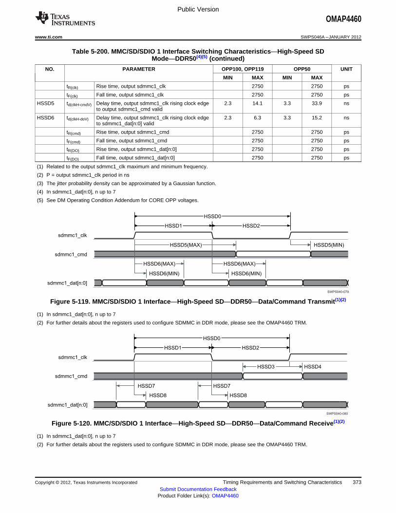
SWPS040-079
sdmmc1_clk
sdmmc1_cmd
sdmmc1_dat[n:0]
HSSD0
HSSD1 HSSD2
HSSD5(MAX) HSSD5(MIN)
HSSD6(MAX)
HSSD6(MIN) HSSD6(MIN)
HSSD6(MAX)
SWPS040-080
sdmmc1_clk
sdmmc1_cmd
sdmmc1_dat[n:0]
HSSD0
HSSD1 HSSD2
HSSD3 HSSD4
HSSD8
HSSD7 HSSD7
HSSD8
Public Version
OMAP4460
www.ti.com SWPS046A –JANUARY 2012
Table 5-200. MMC/SD/SDIO 1 Interface Switching Characteristics—High-Speed SDMode—DDR50(4)(5) (continued)
NO. PARAMETER OPP100, OPP119 OPP50 UNIT
MIN MAX MIN MAX
tR(clk) Rise time, output sdmmc1_clk 2750 2750 ps
tF(clk) Fall time, output sdmmc1_clk 2750 2750 ps
HSSD5 td(clkH-cmdV) Delay time, output sdmmc1_clk rising clock edge 2.3 14.1 3.3 33.9 nsto output sdmmc1_cmd valid
HSSD6 td(clkH-doV) Delay time, output sdmmc1_clk rising clock edge 2.3 6.3 3.3 15.2 nsto sdmmc1_dat[n:0] valid
tR(cmd) Rise time, output sdmmc1_cmd 2750 2750 ps
tF(cmd) Fall time, output sdmmc1_cmd 2750 2750 ps
tR(DO) Rise time, output sdmmc1_dat[n:0] 2750 2750 ps
tF(DO) Fall time, output sdmmc1_dat[n:0] 2750 2750 ps
(1) Related to the output sdmmc1_clk maximum and minimum frequency.
(2) P = output sdmmc1_clk period in ns
(3) The jitter probability density can be approximated by a Gaussian function.
(4) In sdmmc1_dat[n:0], n up to 7
(5) See DM Operating Condition Addendum for CORE OPP voltages.
Figure 5-119. MMC/SD/SDIO 1 Interface—High-Speed SD—DDR50—Data/Command Transmit(1)(2)
(1) In sdmmc1_dat[n:0], n up to 7
(2) For further details about the registers used to configure SDMMC in DDR mode, please see the OMAP4460 TRM.
Figure 5-120. MMC/SD/SDIO 1 Interface—High-Speed SD—DDR50—Data/Command Receive(1)(2)
(1) In sdmmc1_dat[n:0], n up to 7
(2) For further details about the registers used to configure SDMMC in DDR mode, please see the OMAP4460 TRM.
Copyright © 2012, Texas Instruments Incorporated Timing Requirements and Switching Characteristics 373Submit Documentation Feedback
Product Folder Link(s): OMAP4460
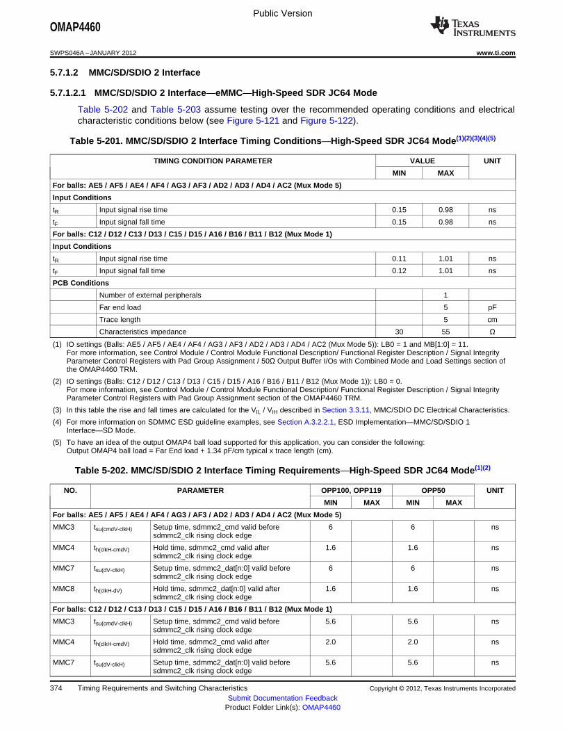
Public Version
OMAP4460
SWPS046A –JANUARY 2012 www.ti.com
5.7.1.2 MMC/SD/SDIO 2 Interface
5.7.1.2.1 MMC/SD/SDIO 2 Interface—eMMC—High-Speed SDR JC64 Mode
Table 5-202 and Table 5-203 assume testing over the recommended operating conditions and electricalcharacteristic conditions below (see Figure 5-121 and Figure 5-122).
Table 5-201. MMC/SD/SDIO 2 Interface Timing Conditions—High-Speed SDR JC64 Mode(1)(2)(3)(4)(5)
TIMING CONDITION PARAMETER VALUE UNIT
MIN MAX
For balls: AE5 / AF5 / AE4 / AF4 / AG3 / AF3 / AD2 / AD3 / AD4 / AC2 (Mux Mode 5)
Input Conditions
tR Input signal rise time 0.15 0.98 ns
tF Input signal fall time 0.15 0.98 ns
For balls: C12 / D12 / C13 / D13 / C15 / D15 / A16 / B16 / B11 / B12 (Mux Mode 1)
Input Conditions
tR Input signal rise time 0.11 1.01 ns
tF Input signal fall time 0.12 1.01 ns
PCB Conditions
Number of external peripherals 1
Far end load 5 pF
Trace length 5 cm
Characteristics impedance 30 55 Ω
(1) IO settings (Balls: AE5 / AF5 / AE4 / AF4 / AG3 / AF3 / AD2 / AD3 / AD4 / AC2 (Mux Mode 5)): LB0 = 1 and MB[1:0] = 11.For more information, see Control Module / Control Module Functional Description/ Functional Register Description / Signal IntegrityParameter Control Registers with Pad Group Assignment / 50Ω Output Buffer I/Os with Combined Mode and Load Settings section ofthe OMAP4460 TRM.
(2) IO settings (Balls: C12 / D12 / C13 / D13 / C15 / D15 / A16 / B16 / B11 / B12 (Mux Mode 1)): LB0 = 0.For more information, see Control Module / Control Module Functional Description/ Functional Register Description / Signal IntegrityParameter Control Registers with Pad Group Assignment section of the OMAP4460 TRM.
(3) In this table the rise and fall times are calculated for the VIL / VIH described in Section 3.3.11, MMC/SDIO DC Electrical Characteristics.
(4) For more information on SDMMC ESD guideline examples, see Section A.3.2.2.1, ESD Implementation—MMC/SD/SDIO 1Interface—SD Mode.
(5) To have an idea of the output OMAP4 ball load supported for this application, you can consider the following:Output OMAP4 ball load = Far End load + 1.34 pF/cm typical x trace length (cm).
Table 5-202. MMC/SD/SDIO 2 Interface Timing Requirements—High-Speed SDR JC64 Mode(1)(2)
NO. PARAMETER OPP100, OPP119 OPP50 UNIT
MIN MAX MIN MAX
For balls: AE5 / AF5 / AE4 / AF4 / AG3 / AF3 / AD2 / AD3 / AD4 / AC2 (Mux Mode 5)
MMC3 tsu(cmdV-clkH) Setup time, sdmmc2_cmd valid before 6 6 nssdmmc2_clk rising clock edge
MMC4 th(clkH-cmdV) Hold time, sdmmc2_cmd valid after 1.6 1.6 nssdmmc2_clk rising clock edge
MMC7 tsu(dV-clkH) Setup time, sdmmc2_dat[n:0] valid before 6 6 nssdmmc2_clk rising clock edge
MMC8 th(clkH-dV) Hold time, sdmmc2_dat[n:0] valid after 1.6 1.6 nssdmmc2_clk rising clock edge
For balls: C12 / D12 / C13 / D13 / C15 / D15 / A16 / B16 / B11 / B12 (Mux Mode 1)
MMC3 tsu(cmdV-clkH) Setup time, sdmmc2_cmd valid before 5.6 5.6 nssdmmc2_clk rising clock edge
MMC4 th(clkH-cmdV) Hold time, sdmmc2_cmd valid after 2.0 2.0 nssdmmc2_clk rising clock edge
MMC7 tsu(dV-clkH) Setup time, sdmmc2_dat[n:0] valid before 5.6 5.6 nssdmmc2_clk rising clock edge
374 Timing Requirements and Switching Characteristics Copyright © 2012, Texas Instruments Incorporated
Submit Documentation FeedbackProduct Folder Link(s): OMAP4460

Public Version
OMAP4460
www.ti.com SWPS046A –JANUARY 2012
Table 5-202. MMC/SD/SDIO 2 Interface Timing Requirements—High-Speed SDR JC64Mode(1)(2) (continued)
NO. PARAMETER OPP100, OPP119 OPP50 UNIT
MIN MAX MIN MAX
MMC8 th(clkH-dV) Hold time, sdmmc2_dat[n:0] valid after 2.0 2.0 nssdmmc2_clk rising clock edge
(1) In sdmmc2_dat[n:0], n up to 7
(2) See DM Operating Condition Addendum for CORE OPP voltages.
Table 5-203. MMC/SD/SDIO Interface 2 Switching Characteristics—High-Speed SDR JC64 Mode(4)(5)(6)
NO. PARAMETER OPP100, OPP119 OPP50 UNIT
MIN MAX MIN MAX
For balls: AE5 / AF5 / AE4 / AF4 / AG3 / AF3 / AD2 / AD3 / AD4 / AC2 (Mux Mode 5)
MMC1 1 / tc(clk) Frequency(1) output sdmmc2_clk 48 48 MHz
MMC2 tw(clkL) Pulse duration, output sdmmc2_clk low 0.5*P(2) 0.5*P(2) ns
MMC2 tw(clkH) Pulse duration, output sdmmc2_clk high 0.5*P(2) 0.5*P(2) ns
tdc(clk) Duty cycle error, output sdmmc2_clk –1042 1042 –1042 1042 ps
tj(clk) Jitter standard deviation(3), output sdmmc2_clk –65 65 –65 65 ps
tR(clk) Rise time, output sdmmc2_clk 2263 2263 ps
tF(clk) Fall time, output sdmmc2_clk 2136 2136 ps
MMC5 td(clkH-cmdV) Delay time, sdmmc2_clk rising clock edge to 3.5 17 3.5 17 nssdmmc2_cmd transition
tR(cmd) Rise time, output sdmmc2_cmd 2263 2263 ps
tF(cmd) Fall time, output sdmmc2_cmd 2136 2136 ps
MMC6 td(clkH-doV) Delay time, sdmmc2_clk rising clock edge to 3.5 17 3.5 17 nssdmmc2_dat[n:0] transition
tR(DO) Rise time, output sdmmc2_dat[n:0] 2263 2263 ps
tF(do) Fall time, output sdmmc2_dat[n:0] 2136 2136 ps
For balls: C12 / D12 / C13 / D13 / C15 / D15 / A16 / B16 / B11 / B12 (Mux Mode 1)
MMC1 1 / tc(clk) Frequency(1) output sdmmc2_clk 48 48 MHz
MMC2 tw(clkL) Pulse duration, output sdmmc2_clk low 0.5*P(2) 0.5*P(2) ns
MMC2 tw(clkH) Pulse duration, output sdmmc2_clk high 0.5*P(2) 0.5*P(2) ns
tdc(clk) Duty cycle error, output sdmmc2_clk –1042 1042 –1042 1042 ps
tj(clk) Jitter standard deviation(3), output sdmmc2_clk –65 65 –65 65 ps
tR(clk) Rise time, output sdmmc2_clk 2263 2263 ps
tF(clk) Fall time, output sdmmc2_clk 2136 2136 ps
MMC5 td(clkH-cmdV) Delay time, sdmmc2_clk rising clock edge to 3.5 16.9 3.5 16.9 nssdmmc2_cmd transition
tR(cmd) Rise time, output sdmmc2_cmd 2263 2263 ps
tF(cmd) Fall time, output sdmmc2_cmd 2136 2136 ps
MMC6 td(clkH-doV) Delay time, sdmmc2_clk rising clock edge to 3.5 16.9 3.5 16.9 nssdmmc2_dat[n:0] transition
tR(DO) Rise time, output sdmmc2_dat[n:0] 2263 2263 ps
tF(do) Fall time, output sdmmc2_dat[n:0] 2136 2136 ps
(1) Related to the output sdmmcx_clk maximum and minimum frequency.
(2) P = output sdmmc2_clk period in ns
(3) The jitter probability density can be approximated by a Gaussian function.
(4) In sdmmc2_dat[n:0], n up to 7
(5) In this section, the MMC/SD/SDIO output data and command signals are driven on the falling clock edge.In this case, the MMCHS_HCTL[2] HSPE bit is set to 0. The controller is by default in this mode to maximize hold timings.For more information, see MMC/SD/SDIO / MMC/SD/SDIO Functional Description / Output Signals Generation / Generation on FallingEdge of MMC Clock section of the OMAP4460 TRM.
Copyright © 2012, Texas Instruments Incorporated Timing Requirements and Switching Characteristics 375Submit Documentation Feedback
Product Folder Link(s): OMAP4460
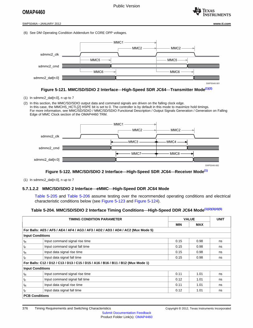
SWPS040-081
sdmmc2_clk
sdmmc2_cmd
sdmmc2_dat[n:0]
MMC5 MMC5
MMC6 MMC6
MMC1
MMC2MMC2
SWPS040-082
sdmmc2_clk
sdmmc2_cmd
sdmmc2_dat[n:0]
MMC4
MMC8
MMC3
MMC7
MMC1
MMC2MMC2
Public Version
OMAP4460
SWPS046A –JANUARY 2012 www.ti.com
(6) See DM Operating Condition Addendum for CORE OPP voltages.
Figure 5-121. MMC/SD/SDIO 2 Interface—High-Speed SDR JC64—Transmitter Mode(1)(2)
(1) In sdmmc2_dat[n:0], n up to 7
(2) In this section, the MMC/SD/SDIO output data and command signals are driven on the falling clock edge.In this case, the MMCHS_HCTL[2] HSPE bit is set to 0. The controller is by default in this mode to maximize hold timings.For more information, see MMC/SD/SDIO / MMC/SD/SDIO Functional Description / Output Signals Generation / Generation on FallingEdge of MMC Clock section of the OMAP4460 TRM.
Figure 5-122. MMC/SD/SDIO 2 Interface—High-Speed SDR JC64—Receiver Mode(1)
(1) In sdmmc2_dat[n:0], n up to 7
5.7.1.2.2 MMC/SD/SDIO 2 Interface—eMMC—High-Speed DDR JC64 Mode
Table 5-205 and Table 5-206 assume testing over the recommended operating conditions and electricalcharacteristic conditions below (see Figure 5-123 and Figure 5-124).
Table 5-204. MMC/SD/SDIO 2 Interface Timing Conditions—High-Speed DDR JC64 Mode(1)(2)(3)(4)(5)
TIMING CONDITION PARAMETER VALUE UNIT
MIN MAX
For Balls: AE5 / AF5 / AE4 / AF4 / AG3 / AF3 / AD2 / AD3 / AD4 / AC2 (Mux Mode 5)
Input Conditions
tR Input command signal rise time 0.15 0.98 ns
tF Input command signal fall time 0.15 0.98 ns
tR Input data signal rise time 0.15 0.98 ns
tF Input data signal fall time 0.15 0.98 ns
For Balls: C12 / D12 / C13 / D13 / C15 / D15 / A16 / B16 / B11 / B12 (Mux Mode 1)
Input Conditions
tR Input command signal rise time 0.11 1.01 ns
tF Input command signal fall time 0.12 1.01 ns
tR Input data signal rise time 0.11 1.01 ns
tF Input data signal fall time 0.12 1.01 ns
PCB Conditions
376 Timing Requirements and Switching Characteristics Copyright © 2012, Texas Instruments Incorporated
Submit Documentation FeedbackProduct Folder Link(s): OMAP4460

Public Version
OMAP4460
www.ti.com SWPS046A –JANUARY 2012
Table 5-204. MMC/SD/SDIO 2 Interface Timing Conditions—High-Speed DDR JC64Mode(1)(2)(3)(4)(5) (continued)
TIMING CONDITION PARAMETER VALUE UNIT
MIN MAX
Number of external peripherals 1
Far end load 5 pF
Trace length 5 cm
Characteristics impedance 30 55 Ω
(1) IO settings (Balls: AE5 / AF5 / AE4 / AF4 / AG3 / AF3 / AD2 / AD3 / AD4 / AC2 (Mux Mode 5)): LB0 = 1 and MB[1:0] = 11.For more information, see Control Module / Control Module Functional Description/ Functional Register Description / Signal IntegrityParameter Control Registers with Pad Group Assignment / 50Ω Output Buffer I/Os with Combined Mode and Load Settings section ofthe OMAP4460 TRM.
(2) IO settings (Balls: C12 / D12 / C13 / D13 / C15 / D15 / A16 / B16 / B11 / B12 (Mux Mode 1)): LB0 = 0.For more information, see Control Module / Control Module Functional Description/ Functional Register Description / Signal IntegrityParameter Control Registers with Pad Group Assignment section of the OMAP4460 TRM.
(3) In this table the rise and fall times are calculated for the VIL / VIH described in Section 3.3.11, MMC/SDIO DC Electrical Characteristics.
(4) For more information on SDMMC ESD guideline examples, see Section A.3.2.2.1, ESD Implementation—MMC/SD/SDIO 1Interface—SD Mode.
(5) To have an idea of the output OMAP4 ball load supported for this application, you can consider the following:Output OMAP4 ball load = Far End load + 1.34 pF/cm typical x trace length (cm).
Table 5-205. MMC/SD/SDIO 2 Interface Timing Requirements—High-Speed DDR JC64 Mode(1)(2)
NO. PARAMETER OPP100, OPP119 OPP50 UNIT
MIN MAX MIN MAX
For Balls: AE5 / AF5 / AE4 / AF4 / AG3 / AF3 / AD2 / AD3 / AD4 / AC2 (Mux Mode 5)
DDReMMC3 tsu(dV-clkH) Setup time, input sdmmc2_cmd valid before 5.5 26 nssdmmc2_clk rising clock edge
DDReMMC4 th(clkH-dV) Hold time, output sdmmc2_cmd valid after 2.4 1.9 nssdmmc2_clk rising clock edge
DDReMMC7 tsu(dV-clkH) Setup time, input sdmmc2_dat[n:0] valid before 0.9 9.9 nssdmmc2_clk rising clock edge
DDReMMC8 th(clkH-dV) Hold time, output sdmmc2_dat[n:0] valid after 1.4 0.9 nssdmmc2_clk rising clock edge
For balls: C12 / D12 / C13 / D13 / C15 / D15 / A16 / B16 / B11 / B12 (Mux Mode 1)
DDReMMC3 tsu(dV-clkH) Setup time, input sdmmc2_cmd valid before 5.5 26 nssdmmc2_clk rising clock edge
DDReMMC4 th(clkH-dV) Hold time, output sdmmc2_cmd valid after 2.4 1.9 nssdmmc2_clk rising clock edge
DDReMMC7 tsu(dV-clkH) Setup time, input sdmmc2_dat[n:0] valid before 1.4 10.4 nssdmmc2_clk rising clock edge
DDReMMC8 th(clkH-dV) Hold time, output sdmmc2_dat[n:0] valid after 0.9 0.4 nssdmmc2_clk rising clock edge
(1) In sdmmc2_dat[n:0], n up to 7
(2) See DM Operating Condition Addendum for CORE OPP voltages.
Table 5-206. MMC/SD/SDIO 2 Interface Switching Characteristics—High-Speed DDR JC64 Mode(4)(5)
NO. PARAMETER OPP100, OPP119 OPP50 UNIT
MIN MAX MIN MAX
For balls: AE5 / AF5 / AE4 / AF4 / AG3 / AF3 / AD2 / AD3 / AD4 / AC2 (Mux Mode 5)
DDReMMC1 1 / tc(clk) Frequency(1) output sdmmc2_clk 48 24 MHz
DDReMMC2 tw(clkL) Pulse duration, output sdmmc2_clk low 0.5*P(2) 0.5*P(2) ns
DDReMMC2 tw(clkH) Pulse duration, output sdmmc2_clk high 0.5*P(2) 0.5*P(2) ns
tdc(clk) Duty cycle error, output sdmmc2_clk –1042 1042 –2083 2083 ps
tj(clk) Jitter standard deviation(3), output sdmmc2_clk –65 65 –65 65 ps
Copyright © 2012, Texas Instruments Incorporated Timing Requirements and Switching Characteristics 377Submit Documentation Feedback
Product Folder Link(s): OMAP4460

SWPS040-083
sdmmc2_clk
sdmmc2_cmd
DDReMMC1
DDReMMC2DDReMMC2
DDReMMC3 DDReMMC4
DDReMMC8 DDReMMC8 DDReMMC8
sdmmc2_dat[n:0]
DDReMMC7DDReMMC7DDReMMC7DDReMMC7
Public Version
OMAP4460
SWPS046A –JANUARY 2012 www.ti.com
Table 5-206. MMC/SD/SDIO 2 Interface Switching Characteristics—High-Speed DDR JC64Mode(4)(5) (continued)
NO. PARAMETER OPP100, OPP119 OPP50 UNIT
MIN MAX MIN MAX
tR(clk) Rise time, output sdmmc2_clk 2263 2263 ps
tF(clk) Fall time, output sdmmc2_clk 2136 2136 ps
DDReMMC5 td(clkH-cmdV) Delay time, sdmmc2_clk rising clock edge to 3.6 16.9 4 37.3 nssdmmc2_cmd transition
tR(cmd) Rise time, output sdmmc2_cmd 2263 2263 ps
tF(cmd) Fall time, output sdmmc2_cmd 2136 2136 ps
DDReMMC6 td(clkH-doV) Delay time, sdmmc2_clk rising clock edge to 3.1 6 3.5 15 nssdmmc2_dat[n:0] transition
tR(DO) Rise time, output sdmmc2_dat[n:0] 2263 2263 ps
tF(do) Fall time, output sdmmc2_dat[n:0] 2136 2136 ps
For balls: C12 / D12 / C13 / D13 / C15 / D15 / A16 / B16 / B11 / B12 (Mux Mode 1)
DDReMMC1 1 / tc(clk) Frequency(1) output sdmmc2_clk 48 24 MHz
DDReMMC2 tw(clkL) Pulse duration, output sdmmc2_clk low 0.5*P(2) 0.5*P(2) ns
DDReMMC2 tw(clkH) Pulse duration, output sdmmc2_clk high 0.5*P(2) 0.5*P(2) ns
tdc(clk) Duty cycle error, output sdmmc2_clk –1042 1042 –2083 2083 ps
tj(clk) Jitter standard deviation(3), output sdmmc2_clk –65 65 –65 65 ps
tR(clk) Rise time, output sdmmc2_clk 2263 2263 ps
tF(clk) Fall time, output sdmmc2_clk 2136 2136 ps
DDReMMC5 td(clkH-cmdV) Delay time, sdmmc2_clk rising clock edge to 3.6 16.9 4 37.3 nssdmmc2_cmd transition
tR(cmd) Rise time, output sdmmc2_cmd 2263 2263 ps
tF(cmd) Fall time, output sdmmc2_cmd 2136 2136 ps
DDReMMC6 td(clkH-doV) Delay time, sdmmc2_clk rising clock edge to 3.1 6 3.5 15 nssdmmc2_dat[n:0] transition
tR(DO) Rise time, output sdmmc2_dat[n:0] 2263 2263 ps
tF(DO) Fall time, output sdmmc2_dat[n:0] 2136 2136 ps
(1) Related to the output sdmmc2_clk maximum and minimum frequency.
(2) P = output sdmmc2_clk period in ns
(3) The jitter probability density can be approximated by a Gaussian function.
(4) In sdmmc2_dat[n:0], n up to 7
(5) See DM Operating Condition Addendum for CORE OPP voltages.
Figure 5-123. MMC/SD/SDIO 2 Interface—High-Speed DDR JC64—Receiver Mode(1)
(1) In sdmmc2_dat[n:0], n up to 7
378 Timing Requirements and Switching Characteristics Copyright © 2012, Texas Instruments Incorporated
Submit Documentation FeedbackProduct Folder Link(s): OMAP4460

SWPS040-084
sdmmc2_clk
sdmmc2_cmd
sdmmc2_dat[n:0]
DDReMMC1
DDReMMC2DDReMMC2
DDReMMC6
DDReMMC5
DDReMMC5
DDReMMC6
DDReMMC6
DDReMMC5
DDReMMC5
DDReMMC6 DDReMMC6
DDReMMC6
Public Version
OMAP4460
www.ti.com SWPS046A –JANUARY 2012
Figure 5-124. MMC/SD/SDIO 2 Interface—High-Speed DDR JC64—Transmitter Mode(1)
(1) In sdmmc2_dat[n:0], n up to 7
5.7.1.2.3 MMC/SD/SDIO 2 Interface—eMMC—Standard SDR JC64 Mode
Table 5-208 and Table 5-209 assume testing over the recommended operating conditions and electricalcharacteristic conditions below (see Figure 5-125 and Figure 5-126).
Table 5-207. MMC/SD/SDIO 2 Interface Timing Conditions—Standard SDR JC64 Mode(1)(2)(3)(4)
TIMING CONDITION PARAMETER VALUE UNIT
MIN MAX
Input Conditions
tR Input signal rise time 0.2 10 ns
tF Input signal fall time 0.2 10 ns
PCB Conditions
Number of external peripherals 1
Far end load 5 pF
Trace length 5 cm
Characteristics impedance 30 55 Ω
(1) IO settings (Balls: C12 / D12 / C13 / D13 / C15 / D15 / A16 / B16 / B11 / B12 (Mux Mode 1)): LB0 = 0.For more information, see Control Module / Control Module Functional Description/ Functional Register Description / Signal IntegrityParameter Control Registers with Pad Group Assignment section of the OMAP4460 TRM.
(2) In this table the rise and fall times are calculated for the VIL / VIH described in Section 3.3.11, MMC/SDIO DC Electrical Characteristics.
(3) For more information on SDMMC ESD guideline examples, see Section A.3.2.2.1, ESD Implementation—MMC/SD/SDIO 1Interface—SD Mode.
(4) To have an idea of the output OMAP4 ball load supported for this application, you can consider the following:Output OMAP4 ball load = Far End load + 1.34 pF/cm typical x trace length (cm).
Table 5-208. MMC/SD/SDIO 2 Interface Timing Requirements—Standard SDR JC64 Mode(1)(2)
NO. PARAMETER OPP100, OPP119 OPP50 UNIT
MIN MAX MIN MAX
MMC3 tsu(cmdV-clkH) Setup time, sdmmc2_cmd valid before 3.5 3.5 nssdmmc2_clk rising clock edge
MMC4 th(clkH-cmdV) Hold time, sdmmc2_cmd valid after 8 8 nssdmmc2_clk rising clock edge
MMC7 tsu(dV-clkH) Setup time, sdmmc2_dat[n:0] valid before 3.5 3.5 nssdmmc2_clk rising clock edge
MMC8 th(clkH-dV) Hold time, sdmmc2_dat[n:0] valid after 8 8 nssdmmc2_clk rising clock edge
Copyright © 2012, Texas Instruments Incorporated Timing Requirements and Switching Characteristics 379Submit Documentation Feedback
Product Folder Link(s): OMAP4460
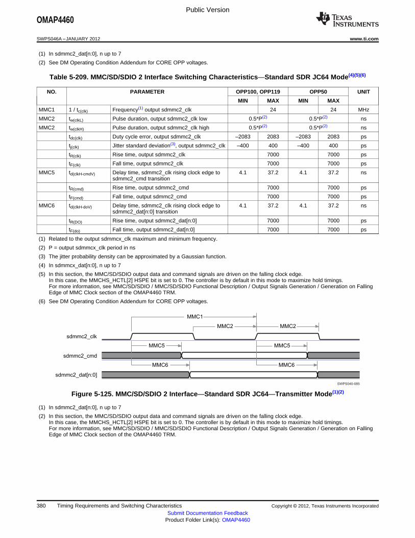
SWPS040-085
sdmmc2_clk
sdmmc2_cmd
sdmmc2_dat[n:0]
MMC5 MMC5
MMC6 MMC6
MMC1
MMC2MMC2
Public Version
OMAP4460
SWPS046A –JANUARY 2012 www.ti.com
(1) In sdmmc2_dat[n:0], n up to 7
(2) See DM Operating Condition Addendum for CORE OPP voltages.
Table 5-209. MMC/SD/SDIO 2 Interface Switching Characteristics—Standard SDR JC64 Mode(4)(5)(6)
NO. PARAMETER OPP100, OPP119 OPP50 UNIT
MIN MAX MIN MAX
MMC1 1 / tc(clk) Frequency(1) output sdmmc2_clk 24 24 MHz
MMC2 tw(clkL) Pulse duration, output sdmmc2_clk low 0.5*P(2) 0.5*P(2) ns
MMC2 tw(clkH) Pulse duration, output sdmmc2_clk high 0.5*P(2) 0.5*P(2) ns
tdc(clk) Duty cycle error, output sdmmc2_clk –2083 2083 –2083 2083 ps
tj(clk) Jitter standard deviation(3), output sdmmc2_clk –400 400 –400 400 ps
tR(clk) Rise time, output sdmmc2_clk 7000 7000 ps
tF(clk) Fall time, output sdmmc2_clk 7000 7000 ps
MMC5 td(clkH-cmdV) Delay time, sdmmc2_clk rising clock edge to 4.1 37.2 4.1 37.2 nssdmmc2_cmd transition
tR(cmd) Rise time, output sdmmc2_cmd 7000 7000 ps
tF(cmd) Fall time, output sdmmc2_cmd 7000 7000 ps
MMC6 td(clkH-doV) Delay time, sdmmc2_clk rising clock edge to 4.1 37.2 4.1 37.2 nssdmmc2_dat[n:0] transition
tR(DO) Rise time, output sdmmc2_dat[n:0] 7000 7000 ps
tF(do) Fall time, output sdmmc2_dat[n:0] 7000 7000 ps
(1) Related to the output sdmmcx_clk maximum and minimum frequency.
(2) P = output sdmmcx_clk period in ns
(3) The jitter probability density can be approximated by a Gaussian function.
(4) In sdmmcx_dat[n:0], n up to 7
(5) In this section, the MMC/SD/SDIO output data and command signals are driven on the falling clock edge.In this case, the MMCHS_HCTL[2] HSPE bit is set to 0. The controller is by default in this mode to maximize hold timings.For more information, see MMC/SD/SDIO / MMC/SD/SDIO Functional Description / Output Signals Generation / Generation on FallingEdge of MMC Clock section of the OMAP4460 TRM.
(6) See DM Operating Condition Addendum for CORE OPP voltages.
Figure 5-125. MMC/SD/SDIO 2 Interface—Standard SDR JC64—Transmitter Mode(1)(2)
(1) In sdmmc2_dat[n:0], n up to 7
(2) In this section, the MMC/SD/SDIO output data and command signals are driven on the falling clock edge.In this case, the MMCHS_HCTL[2] HSPE bit is set to 0. The controller is by default in this mode to maximize hold timings.For more information, see MMC/SD/SDIO / MMC/SD/SDIO Functional Description / Output Signals Generation / Generation on FallingEdge of MMC Clock section of the OMAP4460 TRM.
380 Timing Requirements and Switching Characteristics Copyright © 2012, Texas Instruments Incorporated
Submit Documentation FeedbackProduct Folder Link(s): OMAP4460

SWPS040-086
sdmmc2_clk
sdmmc2_cmd
sdmmc2_dat[n:0]
MMC4
MMC8
MMC3
MMC7
MMC1
MMC2MMC2
Public Version
OMAP4460
www.ti.com SWPS046A –JANUARY 2012
Figure 5-126. MMC/SD/SDIO 2 Interface—Standard SDR JC64—Receiver Mode(1)
(1) In sdmmc2_dat[n:0], n up to 7
5.7.1.3 MMC/SD/SDIO 3, 4, and 5 Interfaces
5.7.1.3.1 MMC/SD/SDIO 3, 4, and 5 Interfaces—High-Speed SDIO Mode
Table 5-211 and Table 5-212 assume testing over the recommended operating conditions and electricalcharacteristic conditions below (see Figure 5-127 and Figure 5-128).
Table 5-210. MMC/SD/SDIO 3, 4, and 5 Interface Timing Conditions—High-Speed SDIO Mode(1)(2)(3)(4)(5)
TIMING CONDITION PARAMETER VALUE UNIT
MIN MAX
For Balls: AB25 / AC27 / AB26 / AB27 / AA25 / AA26 (Mux Mode 1 – Interface 3)For Balls: AE21 / AF20 / AF21 / AE20 / AG20 / AH19 (Mux Mode 1 – Interface 4)For Balls: AE5 / AF5 / AE4 / AF4 / AG3 / AF3 (Mux Mode 0 – Interface 5)
Input Conditions
tR Input signal rise time 0.14 1.18 ns
tF Input signal fall time 0.11 1.18 ns
For balls: AG11 / AH11 / AE10 / AF10 / AG10 / AE9 (Mux Mode 2 – Interface 3)For balls: AG12 / AF12 / AE12 / AG13 / AE11 / AF11 (Mux Mode 2 – Interface 4)
Input Conditions
tR Input signal rise time 0.18 1.67 ns
tF Input signal fall time 0.17 1.58 ns
PCB Conditions
Number of external peripherals 1
Far end load 5 pF
Trace length 5 cm
Characteristics impedance 30 60 Ω
(1) IO settings (For balls: AB25 / AC27 / AB26 / AB27 / AA25 / AA26 (Mux Mode 1 – Interface 3)For balls: AE21 / AF20 / AF21 / AE20 / AG20 / AH19 (Mux Mode 1 – Interface 4)For balls: AE5 / AF5 / AE4 / AF4 / AG3 / AF3 (Mux Mode 0 – Interface 5)): LB0 = 1 and MB[1:0] = 11.For more information, see Control Module / Control Module Functional Description/ Functional Register Description / Signal IntegrityParameter Control Registers with Pad Group Assignment / 50Ω Output Buffer I/Os with Combined Mode and Load Settings section ofthe OMAP4460 TRM.
(2) IO settings (For balls: AG11 / AH11 / AE10 / AF10 / AG10 / AE9 (Mux Mode 2 – Interface 3)For balls: AG12 / AF12 / AE12 / AG13 / AE11 / AF11 (Mux Mode 2 – Interface 4)): DS0 = 0.For more information, see Control Module / Control Module Functional Description/ Functional Register Description / Signal IntegrityParameter Control Registers with Pad Group Assignment / I/O cells with Configurable Output Driver Impedance section of theOMAP4460 TRM.
(3) In this table the rise and fall times are calculated for the VIL / VIH described in Section 3.3.11, MMC/SDIO DC Electrical Characteristics.
(4) For more information on SDMMC ESD guideline examples, see Section A.3.2.2.1, ESD Implementation—MMC/SD/SDIO 1Interface—SD Mode.
(5) To have an idea of the output OMAP4 ball load supported for this application, you can consider the following:Output OMAP4 ball load = Far End load + 1.34 pF/cm typical x trace length (cm).
Copyright © 2012, Texas Instruments Incorporated Timing Requirements and Switching Characteristics 381Submit Documentation Feedback
Product Folder Link(s): OMAP4460
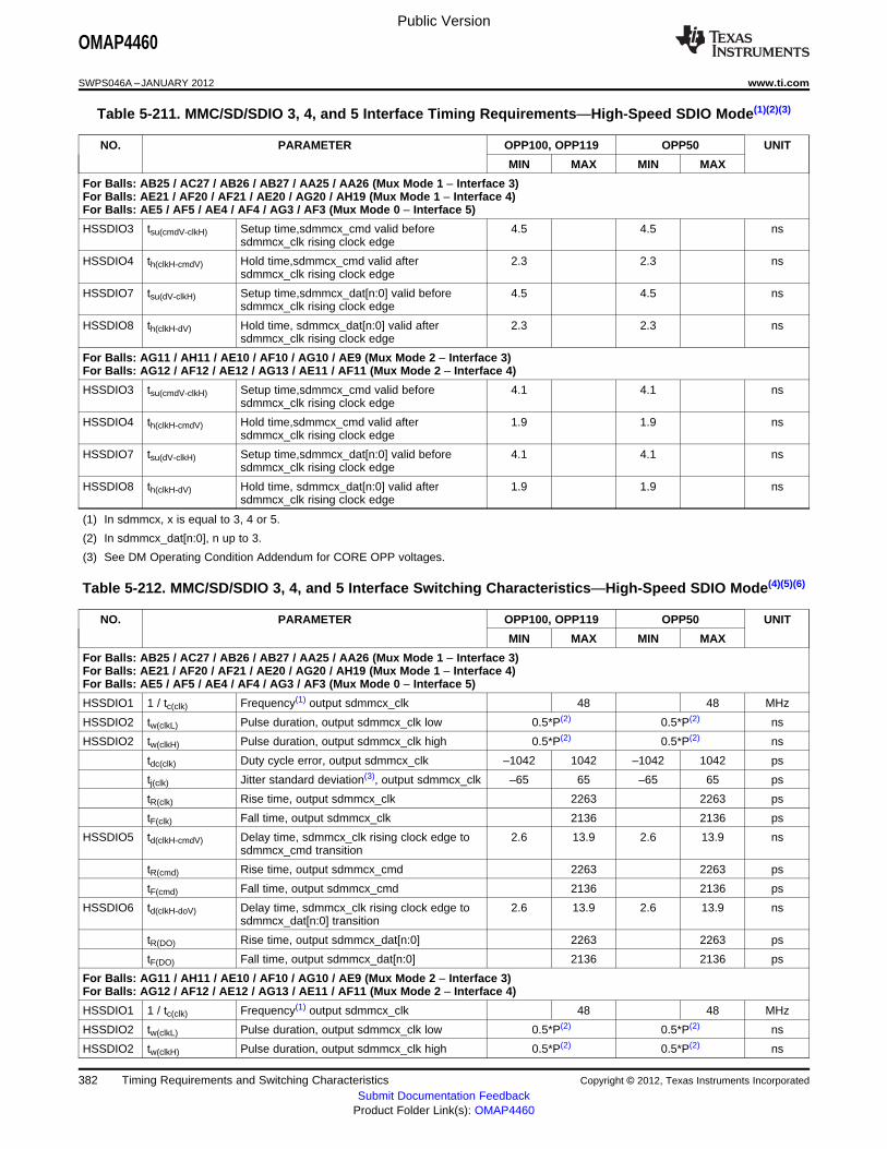
Public Version
OMAP4460
SWPS046A –JANUARY 2012 www.ti.com
Table 5-211. MMC/SD/SDIO 3, 4, and 5 Interface Timing Requirements—High-Speed SDIO Mode(1)(2)(3)
NO. PARAMETER OPP100, OPP119 OPP50 UNIT
MIN MAX MIN MAX
For Balls: AB25 / AC27 / AB26 / AB27 / AA25 / AA26 (Mux Mode 1 – Interface 3)For Balls: AE21 / AF20 / AF21 / AE20 / AG20 / AH19 (Mux Mode 1 – Interface 4)For Balls: AE5 / AF5 / AE4 / AF4 / AG3 / AF3 (Mux Mode 0 – Interface 5)
HSSDIO3 tsu(cmdV-clkH) Setup time,sdmmcx_cmd valid before 4.5 4.5 nssdmmcx_clk rising clock edge
HSSDIO4 th(clkH-cmdV) Hold time,sdmmcx_cmd valid after 2.3 2.3 nssdmmcx_clk rising clock edge
HSSDIO7 tsu(dV-clkH) Setup time,sdmmcx_dat[n:0] valid before 4.5 4.5 nssdmmcx_clk rising clock edge
HSSDIO8 th(clkH-dV) Hold time, sdmmcx_dat[n:0] valid after 2.3 2.3 nssdmmcx_clk rising clock edge
For Balls: AG11 / AH11 / AE10 / AF10 / AG10 / AE9 (Mux Mode 2 – Interface 3)For Balls: AG12 / AF12 / AE12 / AG13 / AE11 / AF11 (Mux Mode 2 – Interface 4)
HSSDIO3 tsu(cmdV-clkH) Setup time,sdmmcx_cmd valid before 4.1 4.1 nssdmmcx_clk rising clock edge
HSSDIO4 th(clkH-cmdV) Hold time,sdmmcx_cmd valid after 1.9 1.9 nssdmmcx_clk rising clock edge
HSSDIO7 tsu(dV-clkH) Setup time,sdmmcx_dat[n:0] valid before 4.1 4.1 nssdmmcx_clk rising clock edge
HSSDIO8 th(clkH-dV) Hold time, sdmmcx_dat[n:0] valid after 1.9 1.9 nssdmmcx_clk rising clock edge
(1) In sdmmcx, x is equal to 3, 4 or 5.
(2) In sdmmcx_dat[n:0], n up to 3.
(3) See DM Operating Condition Addendum for CORE OPP voltages.
Table 5-212. MMC/SD/SDIO 3, 4, and 5 Interface Switching Characteristics—High-Speed SDIO Mode(4)(5)(6)
NO. PARAMETER OPP100, OPP119 OPP50 UNIT
MIN MAX MIN MAX
For Balls: AB25 / AC27 / AB26 / AB27 / AA25 / AA26 (Mux Mode 1 – Interface 3)For Balls: AE21 / AF20 / AF21 / AE20 / AG20 / AH19 (Mux Mode 1 – Interface 4)For Balls: AE5 / AF5 / AE4 / AF4 / AG3 / AF3 (Mux Mode 0 – Interface 5)
HSSDIO1 1 / tc(clk) Frequency(1) output sdmmcx_clk 48 48 MHz
HSSDIO2 tw(clkL) Pulse duration, output sdmmcx_clk low 0.5*P(2) 0.5*P(2) ns
HSSDIO2 tw(clkH) Pulse duration, output sdmmcx_clk high 0.5*P(2) 0.5*P(2) ns
tdc(clk) Duty cycle error, output sdmmcx_clk –1042 1042 –1042 1042 ps
tj(clk) Jitter standard deviation(3), output sdmmcx_clk –65 65 –65 65 ps
tR(clk) Rise time, output sdmmcx_clk 2263 2263 ps
tF(clk) Fall time, output sdmmcx_clk 2136 2136 ps
HSSDIO5 td(clkH-cmdV) Delay time, sdmmcx_clk rising clock edge to 2.6 13.9 2.6 13.9 nssdmmcx_cmd transition
tR(cmd) Rise time, output sdmmcx_cmd 2263 2263 ps
tF(cmd) Fall time, output sdmmcx_cmd 2136 2136 ps
HSSDIO6 td(clkH-doV) Delay time, sdmmcx_clk rising clock edge to 2.6 13.9 2.6 13.9 nssdmmcx_dat[n:0] transition
tR(DO) Rise time, output sdmmcx_dat[n:0] 2263 2263 ps
tF(DO) Fall time, output sdmmcx_dat[n:0] 2136 2136 ps
For Balls: AG11 / AH11 / AE10 / AF10 / AG10 / AE9 (Mux Mode 2 – Interface 3)For Balls: AG12 / AF12 / AE12 / AG13 / AE11 / AF11 (Mux Mode 2 – Interface 4)
HSSDIO1 1 / tc(clk) Frequency(1) output sdmmcx_clk 48 48 MHz
HSSDIO2 tw(clkL) Pulse duration, output sdmmcx_clk low 0.5*P(2) 0.5*P(2) ns
HSSDIO2 tw(clkH) Pulse duration, output sdmmcx_clk high 0.5*P(2) 0.5*P(2) ns
382 Timing Requirements and Switching Characteristics Copyright © 2012, Texas Instruments Incorporated
Submit Documentation FeedbackProduct Folder Link(s): OMAP4460
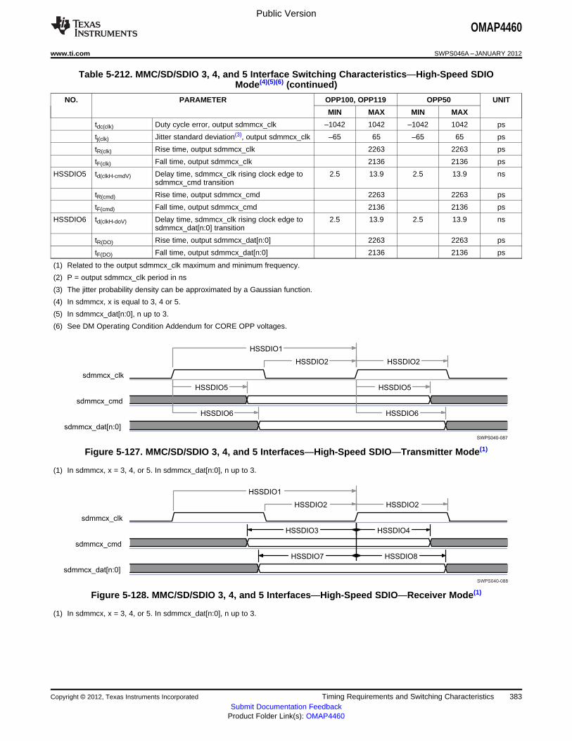
sdmmcx_clk
sdmmcx_cmd
sdmmcx_dat[n:0]
HSSDIO5 HSSDIO5
HSSDIO6 HSSDIO6
HSSDIO1
HSSDIO2HSSDIO2
SWPS040-087
SWPS040-088
sdmmcx_clk
sdmmcx_cmd
sdmmcx_dat[n:0]
HSSDIO4
HSSDIO8
HSSDIO3
HSSDIO7
HSSDIO1
HSSDIO2HSSDIO2
Public Version
OMAP4460
www.ti.com SWPS046A –JANUARY 2012
Table 5-212. MMC/SD/SDIO 3, 4, and 5 Interface Switching Characteristics—High-Speed SDIOMode(4)(5)(6) (continued)
NO. PARAMETER OPP100, OPP119 OPP50 UNIT
MIN MAX MIN MAX
tdc(clk) Duty cycle error, output sdmmcx_clk –1042 1042 –1042 1042 ps
tj(clk) Jitter standard deviation(3), output sdmmcx_clk –65 65 –65 65 ps
tR(clk) Rise time, output sdmmcx_clk 2263 2263 ps
tF(clk) Fall time, output sdmmcx_clk 2136 2136 ps
HSSDIO5 td(clkH-cmdV) Delay time, sdmmcx_clk rising clock edge to 2.5 13.9 2.5 13.9 nssdmmcx_cmd transition
tR(cmd) Rise time, output sdmmcx_cmd 2263 2263 ps
tF(cmd) Fall time, output sdmmcx_cmd 2136 2136 ps
HSSDIO6 td(clkH-doV) Delay time, sdmmcx_clk rising clock edge to 2.5 13.9 2.5 13.9 nssdmmcx_dat[n:0] transition
tR(DO) Rise time, output sdmmcx_dat[n:0] 2263 2263 ps
tF(DO) Fall time, output sdmmcx_dat[n:0] 2136 2136 ps
(1) Related to the output sdmmcx_clk maximum and minimum frequency.
(2) P = output sdmmcx_clk period in ns
(3) The jitter probability density can be approximated by a Gaussian function.
(4) In sdmmcx, x is equal to 3, 4 or 5.
(5) In sdmmcx_dat[n:0], n up to 3.
(6) See DM Operating Condition Addendum for CORE OPP voltages.
Figure 5-127. MMC/SD/SDIO 3, 4, and 5 Interfaces—High-Speed SDIO—Transmitter Mode(1)
(1) In sdmmcx, x = 3, 4, or 5. In sdmmcx_dat[n:0], n up to 3.
Figure 5-128. MMC/SD/SDIO 3, 4, and 5 Interfaces—High-Speed SDIO—Receiver Mode(1)
(1) In sdmmcx, x = 3, 4, or 5. In sdmmcx_dat[n:0], n up to 3.
Copyright © 2012, Texas Instruments Incorporated Timing Requirements and Switching Characteristics 383Submit Documentation Feedback
Product Folder Link(s): OMAP4460
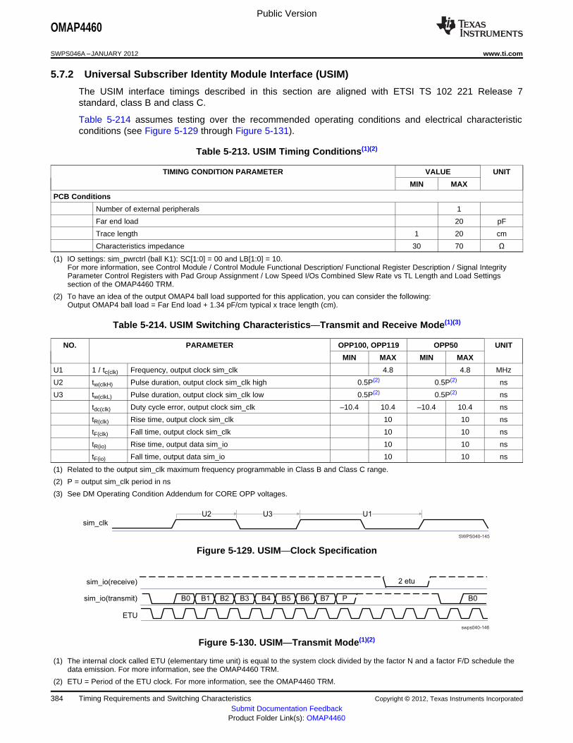
sim_clk
U2 U1U3
SWPS040-145
sim_io(receive) 2 etu
B0 B1 B2 B3 B4 B5 B6 B7 P B0
ETU
sim_io(transmit)
swps040-146
Public Version
OMAP4460
SWPS046A –JANUARY 2012 www.ti.com
5.7.2 Universal Subscriber Identity Module Interface (USIM)
The USIM interface timings described in this section are aligned with ETSI TS 102 221 Release 7standard, class B and class C.
Table 5-214 assumes testing over the recommended operating conditions and electrical characteristicconditions (see Figure 5-129 through Figure 5-131).
Table 5-213. USIM Timing Conditions(1)(2)
TIMING CONDITION PARAMETER VALUE UNIT
MIN MAX
PCB Conditions
Number of external peripherals 1
Far end load 20 pF
Trace length 1 20 cm
Characteristics impedance 30 70 Ω
(1) IO settings: sim_pwrctrl (ball K1): SC[1:0] = 00 and LB[1:0] = 10.For more information, see Control Module / Control Module Functional Description/ Functional Register Description / Signal IntegrityParameter Control Registers with Pad Group Assignment / Low Speed I/Os Combined Slew Rate vs TL Length and Load Settingssection of the OMAP4460 TRM.
(2) To have an idea of the output OMAP4 ball load supported for this application, you can consider the following:Output OMAP4 ball load = Far End load + 1.34 pF/cm typical x trace length (cm).
Table 5-214. USIM Switching Characteristics—Transmit and Receive Mode(1)(3)
NO. PARAMETER OPP100, OPP119 OPP50 UNIT
MIN MAX MIN MAX
U1 1 / tc(clk) Frequency, output clock sim_clk 4.8 4.8 MHz
U2 tw(clkH) Pulse duration, output clock sim_clk high 0.5P(2) 0.5P(2) ns
U3 tw(clkL) Pulse duration, output clock sim_clk low 0.5P(2) 0.5P(2) ns
tdc(clk) Duty cycle error, output clock sim_clk –10.4 10.4 –10.4 10.4 ns
tR(clk) Rise time, output clock sim_clk 10 10 ns
tF(clk) Fall time, output clock sim_clk 10 10 ns
tR(io) Rise time, output data sim_io 10 10 ns
tF(io) Fall time, output data sim_io 10 10 ns
(1) Related to the output sim_clk maximum frequency programmable in Class B and Class C range.
(2) P = output sim_clk period in ns
(3) See DM Operating Condition Addendum for CORE OPP voltages.
Figure 5-129. USIM—Clock Specification
Figure 5-130. USIM—Transmit Mode(1)(2)
(1) The internal clock called ETU (elementary time unit) is equal to the system clock divided by the factor N and a factor F/D schedule thedata emission. For more information, see the OMAP4460 TRM.
(2) ETU = Period of the ETU clock. For more information, see the OMAP4460 TRM.
384 Timing Requirements and Switching Characteristics Copyright © 2012, Texas Instruments Incorporated
Submit Documentation FeedbackProduct Folder Link(s): OMAP4460
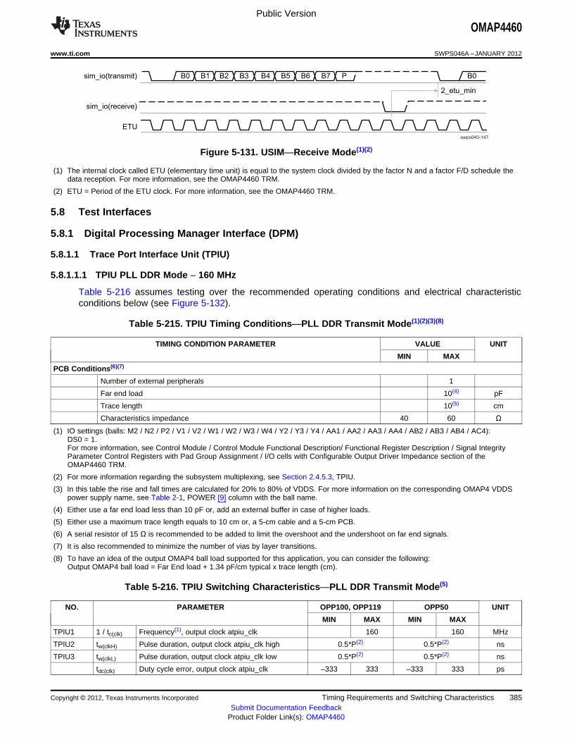
sim_io(receive)
2_etu_min
B0 B1 B2 B3 B4 B5 B6 B7 P B0
ETU
sim_io(transmit)
swps040-147
Public Version
OMAP4460
www.ti.com SWPS046A –JANUARY 2012
Figure 5-131. USIM—Receive Mode(1)(2)
(1) The internal clock called ETU (elementary time unit) is equal to the system clock divided by the factor N and a factor F/D schedule thedata reception. For more information, see the OMAP4460 TRM.
(2) ETU = Period of the ETU clock. For more information, see the OMAP4460 TRM.
5.8 Test Interfaces
5.8.1 Digital Processing Manager Interface (DPM)
5.8.1.1 Trace Port Interface Unit (TPIU)
5.8.1.1.1 TPIU PLL DDR Mode – 160 MHz
Table 5-216 assumes testing over the recommended operating conditions and electrical characteristicconditions below (see Figure 5-132).
Table 5-215. TPIU Timing Conditions—PLL DDR Transmit Mode(1)(2)(3)(8)
TIMING CONDITION PARAMETER VALUE UNIT
MIN MAX
PCB Conditions(6)(7)
Number of external peripherals 1
Far end load 10(4) pF
Trace length 10(5) cm
Characteristics impedance 40 60 Ω
(1) IO settings (balls: M2 / N2 / P2 / V1 / V2 / W1 / W2 / W3 / W4 / Y2 / Y3 / Y4 / AA1 / AA2 / AA3 / AA4 / AB2 / AB3 / AB4 / AC4):DS0 = 1.For more information, see Control Module / Control Module Functional Description/ Functional Register Description / Signal IntegrityParameter Control Registers with Pad Group Assignment / I/O cells with Configurable Output Driver Impedance section of theOMAP4460 TRM.
(2) For more information regarding the subsystem multiplexing, see Section 2.4.5.3, TPIU.
(3) In this table the rise and fall times are calculated for 20% to 80% of VDDS. For more information on the corresponding OMAP4 VDDSpower supply name, see Table 2-1, POWER [9] column with the ball name.
(4) Either use a far end load less than 10 pF or, add an external buffer in case of higher loads.
(5) Either use a maximum trace length equals to 10 cm or, a 5-cm cable and a 5-cm PCB.
(6) A serial resistor of 15 Ω is recommended to be added to limit the overshoot and the undershoot on far end signals.
(7) It is also recommended to minimize the number of vias by layer transitions.
(8) To have an idea of the output OMAP4 ball load supported for this application, you can consider the following:Output OMAP4 ball load = Far End load + 1.34 pF/cm typical x trace length (cm).
Table 5-216. TPIU Switching Characteristics—PLL DDR Transmit Mode(5)
NO. PARAMETER OPP100, OPP119 OPP50 UNIT
MIN MAX MIN MAX
TPIU1 1 / tc(clk) Frequency(1), output clock atpiu_clk 160 160 MHz
TPIU2 tw(clkH) Pulse duration, output clock atpiu_clk high 0.5*P(2) 0.5*P(2) ns
TPIU3 tw(clkL) Pulse duration, output clock atpiu_clk low 0.5*P(2) 0.5*P(2) ns
tdc(clk) Duty cycle error, output clock atpiu_clk –333 333 –333 333 ps
Copyright © 2012, Texas Instruments Incorporated Timing Requirements and Switching Characteristics 385Submit Documentation Feedback
Product Folder Link(s): OMAP4460

SWPS040-089
atpiu_clk
atpiu_cntl
atpiu_d[X:0]
TPIU4 TPIU4
TPIU2
TPIU1
TPIU3
TPIU5 TPIU5
Public Version
OMAP4460
SWPS046A –JANUARY 2012 www.ti.com
Table 5-216. TPIU Switching Characteristics—PLL DDR Transmit Mode(5) (continued)
NO. PARAMETER OPP100, OPP119 OPP50 UNIT
MIN MAX MIN MAX
tj(clk) Jitter standard deviation(3), output clock atpiu_clk 65 65 ps
tR(clk) Rise time, output clock atpiu_clk 2.62 2.62 ns
tF(clk) Fall time, output clock atpiu_clk 2 2 ns
TPIU4 td(clk-ctlV) Delay time, output clock atpiu_clk low/high to 0.884 0.884 nsoutput control atpiu_cntl transition
TPIU5 td(clk-dataV) Delay time, output clock atpiu_clk low/high to 0.884 0.884 nsoutput data atpiu_d[n:0](4) transition
tR(DO) Rise time, output data atpiu_d[n:0](4) and output 2.62 2.62 nscontrol atpiu_cntl
tF(DO) Fall time, output data atpiu_d[n:0](4) and output 2 2 nscontrol atpiu_cntl
(1) Related to the atpiu_clk maximum frequency.
(2) P = atpiu_clk period in ns
(3) The jitter probability density can be approximated by a Gaussian function.
(4) In atpiu_d[n:0], n is equal to 15 or 17.
(5) See DM Operating Condition Addendum for CORE OPP voltages.
Figure 5-132. TPIU—PLL DDR Transmit Mode(1)
(1) In d[X:0], X is equal to 15 or 17.
5.8.1.2 System Trace Module Interface (STM)
The System Trace Module interface (STM) module provides real-time software tracing functionality to theOMAP4460 device.
The trace interface has four trace data pins and a trace clock pin.
This interface is a dual edge interface:• The data are available on rising and falling edge of STM clock.• But can be also configured in single-edge mode where data are available on the falling edge of STM
clock.
Serial interface operates in clock stop regime: serial clock is not free-running; when there is no trace data,there is no trace clock.
5.8.1.2.1 STM – Lauterbach DDR Transmit Mode
Table 5-218 assumes testing over the recommended operating conditions and electrical characteristicconditions below (see Figure 5-133).
386 Timing Requirements and Switching Characteristics Copyright © 2012, Texas Instruments Incorporated
Submit Documentation FeedbackProduct Folder Link(s): OMAP4460
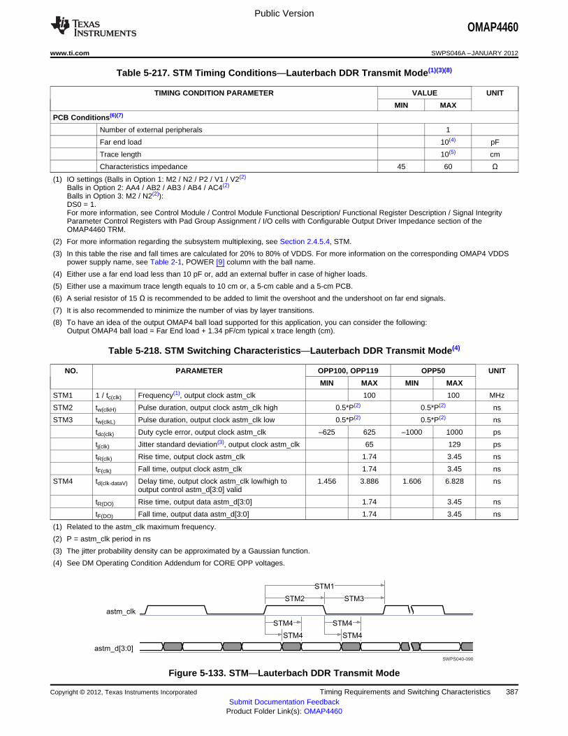
SWPS040-090
astm_clk
astm_d[3:0]
STM2
STM1
STM3
STM4 STM4
STM4 STM4
Public Version
OMAP4460
www.ti.com SWPS046A –JANUARY 2012
Table 5-217. STM Timing Conditions—Lauterbach DDR Transmit Mode(1)(3)(8)
TIMING CONDITION PARAMETER VALUE UNIT
MIN MAX
PCB Conditions(6)(7)
Number of external peripherals 1
Far end load 10(4) pF
Trace length 10(5) cm
Characteristics impedance 45 60 Ω
(1) IO settings (Balls in Option 1: M2 / N2 / P2 / V1 / V2(2)
Balls in Option 2: AA4 / AB2 / AB3 / AB4 / AC4(2)
Balls in Option 3: M2 / N2(2)):DS0 = 1.For more information, see Control Module / Control Module Functional Description/ Functional Register Description / Signal IntegrityParameter Control Registers with Pad Group Assignment / I/O cells with Configurable Output Driver Impedance section of theOMAP4460 TRM.
(2) For more information regarding the subsystem multiplexing, see Section 2.4.5.4, STM.
(3) In this table the rise and fall times are calculated for 20% to 80% of VDDS. For more information on the corresponding OMAP4 VDDSpower supply name, see Table 2-1, POWER [9] column with the ball name.
(4) Either use a far end load less than 10 pF or, add an external buffer in case of higher loads.
(5) Either use a maximum trace length equals to 10 cm or, a 5-cm cable and a 5-cm PCB.
(6) A serial resistor of 15 Ω is recommended to be added to limit the overshoot and the undershoot on far end signals.
(7) It is also recommended to minimize the number of vias by layer transitions.
(8) To have an idea of the output OMAP4 ball load supported for this application, you can consider the following:Output OMAP4 ball load = Far End load + 1.34 pF/cm typical x trace length (cm).
Table 5-218. STM Switching Characteristics—Lauterbach DDR Transmit Mode(4)
NO. PARAMETER OPP100, OPP119 OPP50 UNIT
MIN MAX MIN MAX
STM1 1 / tc(clk) Frequency(1), output clock astm_clk 100 100 MHz
STM2 tw(clkH) Pulse duration, output clock astm_clk high 0.5*P(2) 0.5*P(2) ns
STM3 tw(clkL) Pulse duration, output clock astm_clk low 0.5*P(2) 0.5*P(2) ns
tdc(clk) Duty cycle error, output clock astm_clk –625 625 –1000 1000 ps
tj(clk) Jitter standard deviation(3), output clock astm_clk 65 129 ps
tR(clk) Rise time, output clock astm_clk 1.74 3.45 ns
tF(clk) Fall time, output clock astm_clk 1.74 3.45 ns
STM4 td(clk-dataV) Delay time, output clock astm_clk low/high to 1.456 3.886 1.606 6.828 nsoutput control astm_d[3:0] valid
tR(DO) Rise time, output data astm_d[3:0] 1.74 3.45 ns
tF(DO) Fall time, output data astm_d[3:0] 1.74 3.45 ns
(1) Related to the astm_clk maximum frequency.
(2) P = astm_clk period in ns
(3) The jitter probability density can be approximated by a Gaussian function.
(4) See DM Operating Condition Addendum for CORE OPP voltages.
Figure 5-133. STM—Lauterbach DDR Transmit Mode
Copyright © 2012, Texas Instruments Incorporated Timing Requirements and Switching Characteristics 387Submit Documentation Feedback
Product Folder Link(s): OMAP4460
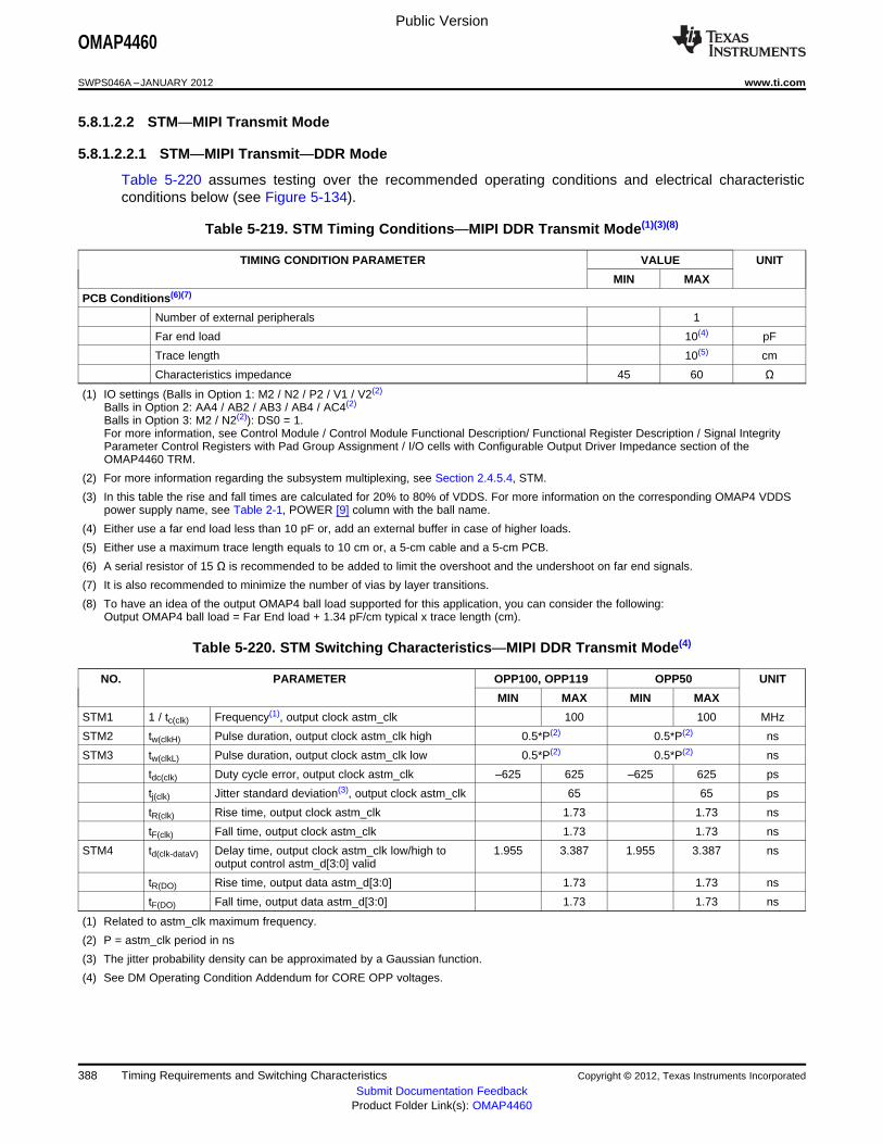
Public Version
OMAP4460
SWPS046A –JANUARY 2012 www.ti.com
5.8.1.2.2 STM—MIPI Transmit Mode
5.8.1.2.2.1 STM—MIPI Transmit—DDR Mode
Table 5-220 assumes testing over the recommended operating conditions and electrical characteristicconditions below (see Figure 5-134).
Table 5-219. STM Timing Conditions—MIPI DDR Transmit Mode(1)(3)(8)
TIMING CONDITION PARAMETER VALUE UNIT
MIN MAX
PCB Conditions(6)(7)
Number of external peripherals 1
Far end load 10(4) pF
Trace length 10(5) cm
Characteristics impedance 45 60 Ω
(1) IO settings (Balls in Option 1: M2 / N2 / P2 / V1 / V2(2)
Balls in Option 2: AA4 / AB2 / AB3 / AB4 / AC4(2)
Balls in Option 3: M2 / N2(2)): DS0 = 1.For more information, see Control Module / Control Module Functional Description/ Functional Register Description / Signal IntegrityParameter Control Registers with Pad Group Assignment / I/O cells with Configurable Output Driver Impedance section of theOMAP4460 TRM.
(2) For more information regarding the subsystem multiplexing, see Section 2.4.5.4, STM.
(3) In this table the rise and fall times are calculated for 20% to 80% of VDDS. For more information on the corresponding OMAP4 VDDSpower supply name, see Table 2-1, POWER [9] column with the ball name.
(4) Either use a far end load less than 10 pF or, add an external buffer in case of higher loads.
(5) Either use a maximum trace length equals to 10 cm or, a 5-cm cable and a 5-cm PCB.
(6) A serial resistor of 15 Ω is recommended to be added to limit the overshoot and the undershoot on far end signals.
(7) It is also recommended to minimize the number of vias by layer transitions.
(8) To have an idea of the output OMAP4 ball load supported for this application, you can consider the following:Output OMAP4 ball load = Far End load + 1.34 pF/cm typical x trace length (cm).
Table 5-220. STM Switching Characteristics—MIPI DDR Transmit Mode(4)
NO. PARAMETER OPP100, OPP119 OPP50 UNIT
MIN MAX MIN MAX
STM1 1 / tc(clk) Frequency(1), output clock astm_clk 100 100 MHz
STM2 tw(clkH) Pulse duration, output clock astm_clk high 0.5*P(2) 0.5*P(2) ns
STM3 tw(clkL) Pulse duration, output clock astm_clk low 0.5*P(2) 0.5*P(2) ns
tdc(clk) Duty cycle error, output clock astm_clk –625 625 –625 625 ps
tj(clk) Jitter standard deviation(3), output clock astm_clk 65 65 ps
tR(clk) Rise time, output clock astm_clk 1.73 1.73 ns
tF(clk) Fall time, output clock astm_clk 1.73 1.73 ns
STM4 td(clk-dataV) Delay time, output clock astm_clk low/high to 1.955 3.387 1.955 3.387 nsoutput control astm_d[3:0] valid
tR(DO) Rise time, output data astm_d[3:0] 1.73 1.73 ns
tF(DO) Fall time, output data astm_d[3:0] 1.73 1.73 ns
(1) Related to astm_clk maximum frequency.
(2) P = astm_clk period in ns
(3) The jitter probability density can be approximated by a Gaussian function.
(4) See DM Operating Condition Addendum for CORE OPP voltages.
388 Timing Requirements and Switching Characteristics Copyright © 2012, Texas Instruments Incorporated
Submit Documentation FeedbackProduct Folder Link(s): OMAP4460
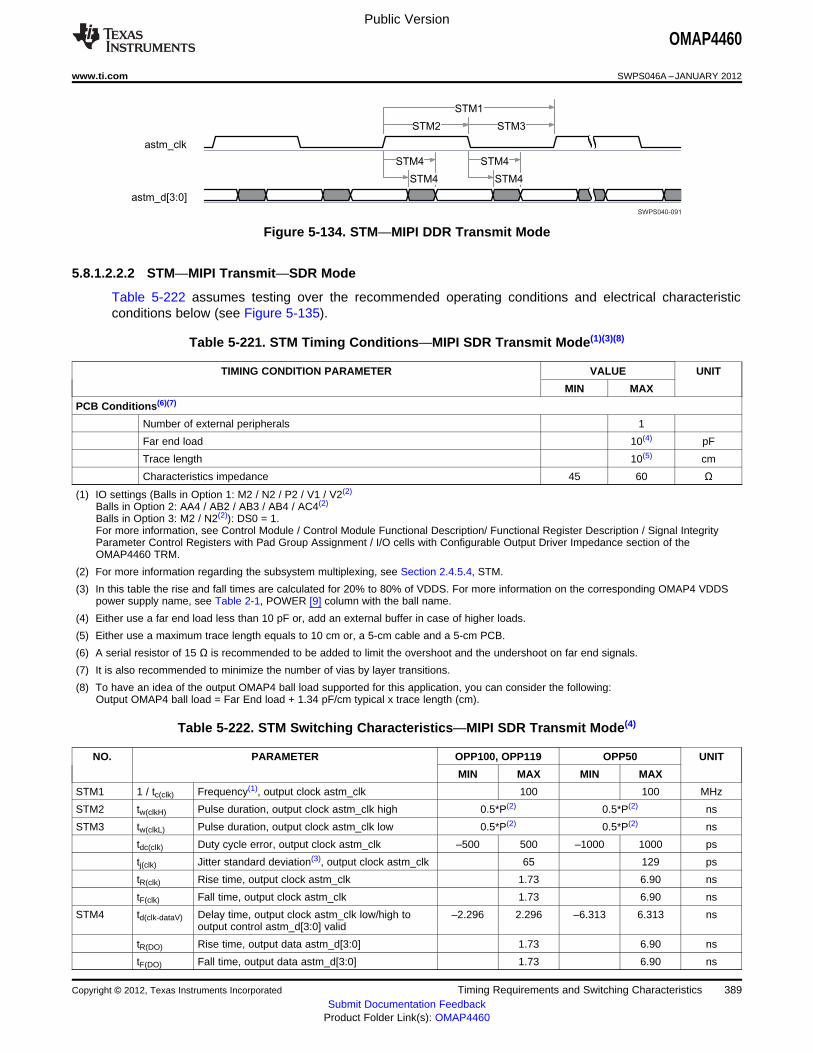
SWPS040-091
astm_clk
astm_d[3:0]
STM2
STM1
STM3
STM4 STM4
STM4 STM4
Public Version
OMAP4460
www.ti.com SWPS046A –JANUARY 2012
Figure 5-134. STM—MIPI DDR Transmit Mode
5.8.1.2.2.2 STM—MIPI Transmit—SDR Mode
Table 5-222 assumes testing over the recommended operating conditions and electrical characteristicconditions below (see Figure 5-135).
Table 5-221. STM Timing Conditions—MIPI SDR Transmit Mode(1)(3)(8)
TIMING CONDITION PARAMETER VALUE UNIT
MIN MAX
PCB Conditions(6)(7)
Number of external peripherals 1
Far end load 10(4) pF
Trace length 10(5) cm
Characteristics impedance 45 60 Ω
(1) IO settings (Balls in Option 1: M2 / N2 / P2 / V1 / V2(2)
Balls in Option 2: AA4 / AB2 / AB3 / AB4 / AC4(2)
Balls in Option 3: M2 / N2(2)): DS0 = 1.For more information, see Control Module / Control Module Functional Description/ Functional Register Description / Signal IntegrityParameter Control Registers with Pad Group Assignment / I/O cells with Configurable Output Driver Impedance section of theOMAP4460 TRM.
(2) For more information regarding the subsystem multiplexing, see Section 2.4.5.4, STM.
(3) In this table the rise and fall times are calculated for 20% to 80% of VDDS. For more information on the corresponding OMAP4 VDDSpower supply name, see Table 2-1, POWER [9] column with the ball name.
(4) Either use a far end load less than 10 pF or, add an external buffer in case of higher loads.
(5) Either use a maximum trace length equals to 10 cm or, a 5-cm cable and a 5-cm PCB.
(6) A serial resistor of 15 Ω is recommended to be added to limit the overshoot and the undershoot on far end signals.
(7) It is also recommended to minimize the number of vias by layer transitions.
(8) To have an idea of the output OMAP4 ball load supported for this application, you can consider the following:Output OMAP4 ball load = Far End load + 1.34 pF/cm typical x trace length (cm).
Table 5-222. STM Switching Characteristics—MIPI SDR Transmit Mode(4)
NO. PARAMETER OPP100, OPP119 OPP50 UNIT
MIN MAX MIN MAX
STM1 1 / tc(clk) Frequency(1), output clock astm_clk 100 100 MHz
STM2 tw(clkH) Pulse duration, output clock astm_clk high 0.5*P(2) 0.5*P(2) ns
STM3 tw(clkL) Pulse duration, output clock astm_clk low 0.5*P(2) 0.5*P(2) ns
tdc(clk) Duty cycle error, output clock astm_clk –500 500 –1000 1000 ps
tj(clk) Jitter standard deviation(3), output clock astm_clk 65 129 ps
tR(clk) Rise time, output clock astm_clk 1.73 6.90 ns
tF(clk) Fall time, output clock astm_clk 1.73 6.90 ns
STM4 td(clk-dataV) Delay time, output clock astm_clk low/high to –2.296 2.296 –6.313 6.313 nsoutput control astm_d[3:0] valid
tR(DO) Rise time, output data astm_d[3:0] 1.73 6.90 ns
tF(DO) Fall time, output data astm_d[3:0] 1.73 6.90 ns
Copyright © 2012, Texas Instruments Incorporated Timing Requirements and Switching Characteristics 389Submit Documentation Feedback
Product Folder Link(s): OMAP4460
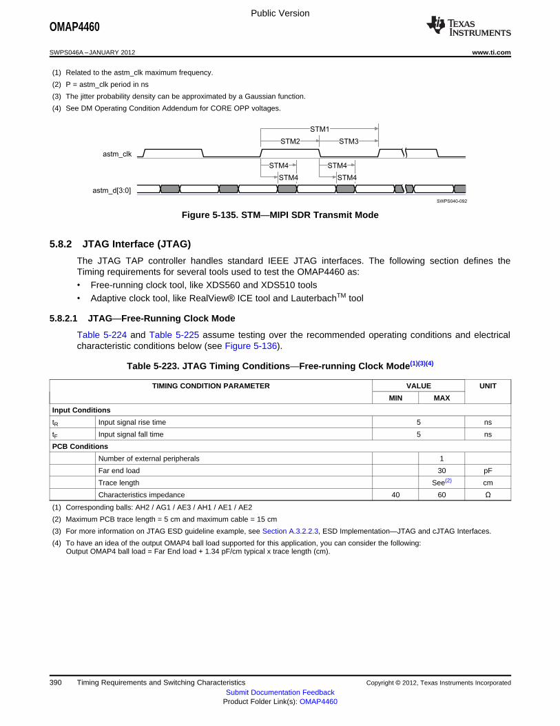
astm_clk
astm_d[3:0]
STM2
STM1
STM3
STM4 STM4
STM4 STM4
SWPS040-092
Public Version
OMAP4460
SWPS046A –JANUARY 2012 www.ti.com
(1) Related to the astm_clk maximum frequency.
(2) P = astm_clk period in ns
(3) The jitter probability density can be approximated by a Gaussian function.
(4) See DM Operating Condition Addendum for CORE OPP voltages.
Figure 5-135. STM—MIPI SDR Transmit Mode
5.8.2 JTAG Interface (JTAG)
The JTAG TAP controller handles standard IEEE JTAG interfaces. The following section defines theTiming requirements for several tools used to test the OMAP4460 as:• Free-running clock tool, like XDS560 and XDS510 tools• Adaptive clock tool, like RealView® ICE tool and LauterbachTM tool
5.8.2.1 JTAG—Free-Running Clock Mode
Table 5-224 and Table 5-225 assume testing over the recommended operating conditions and electricalcharacteristic conditions below (see Figure 5-136).
Table 5-223. JTAG Timing Conditions—Free-running Clock Mode(1)(3)(4)
TIMING CONDITION PARAMETER VALUE UNIT
MIN MAX
Input Conditions
tR Input signal rise time 5 ns
tF Input signal fall time 5 ns
PCB Conditions
Number of external peripherals 1
Far end load 30 pF
Trace length See(2) cm
Characteristics impedance 40 60 Ω
(1) Corresponding balls: AH2 / AG1 / AE3 / AH1 / AE1 / AE2
(2) Maximum PCB trace length = 5 cm and maximum cable = 15 cm
(3) For more information on JTAG ESD guideline example, see Section A.3.2.2.3, ESD Implementation—JTAG and cJTAG Interfaces.
(4) To have an idea of the output OMAP4 ball load supported for this application, you can consider the following:Output OMAP4 ball load = Far End load + 1.34 pF/cm typical x trace length (cm).
390 Timing Requirements and Switching Characteristics Copyright © 2012, Texas Instruments Incorporated
Submit Documentation FeedbackProduct Folder Link(s): OMAP4460

Public Version
OMAP4460
www.ti.com SWPS046A –JANUARY 2012
Table 5-224. JTAG Timing Requirements—Free-running Clock Mode(4)(5)
NO. PARAMETER OPP100, OPP119 OPP50 UNIT
MIN MAX MIN MAX
JT4 1 / tc(tck) Frequency(1), input clock jtag_tck 20 15 MHz
JT5 tw(tckL) Pulse duration, input clock jtag_tck low 0.5*P(2) 0.5*P(2) ns
JT6 tw(tckH) Pulse duration, input clock jtag_tck high 0.5*P(2) 0.5*P(2) ns
tdc(tck) Duty cycle error, input clock jtag_tck –2500.0 2500.0 –3333.0 3333.0 ps
tj(tck) Cycle jitter(3), input clock jtag_tck –2500.0 2500.0 –3333.0 3333.0 ps
JT7 tsu(tdiV-rtckH) Setup time, input data jtag_tdi valid before 1.8 9.0 nsoutput clock jtag_rtck high
JT8 th(tdiV-rtckH) Hold time, input data jtag_tdi valid after output 1.5 2.0 nsclock jtag_rtck high
JT9 tsu(tmsV-rtckH) Setup time, input mode select jtag_tms_tmsc 1.8 9.0 nsvalid before output clock jtag_rtck high
JT10 th(tmsV-rtckH) Hold time, input mode select jtag_tms_tmsc 1.5 2.0 nsvalid after output clock jtag_rtck high
(1) Related to the input maximum frequency supported by the JTAG module.
(2) P = jtag_tck period in ns
(3) Maximum cycle jitter supported by jtag_tck input clock.
(4) The timing requirements are assured for the cycle jitter and duty cycle error conditions specified.
(5) See DM Operating Condition Addendum for CORE OPP voltages.
Table 5-225. JTAG Switching Characteristics—Free-running Clock Mode(4)
NO. PARAMETER OPP100, OPP119 OPP50 UNIT
MIN MAX MIN MAX
JT1 1 / tc(rtck) Frequency(1), output clock jtag_rtck 20 15 MHz
JT2 tw(rtckL) Pulse duration, output clock jtag_rtck low 0.5*PO(2) 0.5*PO(2) ns
JT3 tw(rtckH) Pulse duration, output clock jtag_rtck high 0.5*PO(2) 0.5*PO(2) ns
tdc(rtck) Duty cycle error, output clock jtag_rtck –2500.0 2500.0 –3333.0 3333.0 ps
tj(rtck) Jitter standard deviation(3), output clock 33.3 33.3 psjtag_rtck
tR(rtck) Rise time, output clock jtag_rtck 4.0 4.0 ns
tF(rtck) Fall time, output clock jtag_rtck 4.0 4.0 ns
JT11 td(rtckL-tdoV) Delay time, output clock jtag_rtck low to output –9.3 12.1 –16.4 16.4 nsdata jtag_tdo valid
tR(tdo) Rise time, output data jtag_tdo 4.0 4.0 ns
tF(tdo) Fall time, output data jtag_tdo 4.0 4.0 ns
(1) Related to the jtag_rtck maximum frequency.
(2) PO = jtag_rtck period in ns
(3) The jitter probability density can be approximated by a Gaussian function.
(4) See DM Operating Condition Addendum for CORE OPP voltages.
Copyright © 2012, Texas Instruments Incorporated Timing Requirements and Switching Characteristics 391Submit Documentation Feedback
Product Folder Link(s): OMAP4460
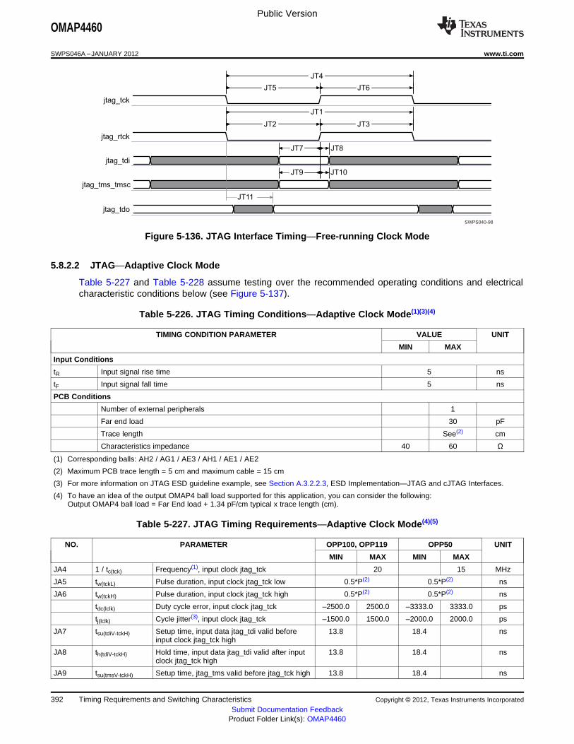
jtag_tck
jtag_rtck
jtag_tdi
jtag_tms_tmsc
jtag_tdo
JT7
JT11
JT1
JT2 JT3
JT8
JT10JT9
JT4
JT5 JT6
SWPS040-98
Public Version
OMAP4460
SWPS046A –JANUARY 2012 www.ti.com
Figure 5-136. JTAG Interface Timing—Free-running Clock Mode
5.8.2.2 JTAG—Adaptive Clock Mode
Table 5-227 and Table 5-228 assume testing over the recommended operating conditions and electricalcharacteristic conditions below (see Figure 5-137).
Table 5-226. JTAG Timing Conditions—Adaptive Clock Mode(1)(3)(4)
TIMING CONDITION PARAMETER VALUE UNIT
MIN MAX
Input Conditions
tR Input signal rise time 5 ns
tF Input signal fall time 5 ns
PCB Conditions
Number of external peripherals 1
Far end load 30 pF
Trace length See(2) cm
Characteristics impedance 40 60 Ω
(1) Corresponding balls: AH2 / AG1 / AE3 / AH1 / AE1 / AE2
(2) Maximum PCB trace length = 5 cm and maximum cable = 15 cm
(3) For more information on JTAG ESD guideline example, see Section A.3.2.2.3, ESD Implementation—JTAG and cJTAG Interfaces.
(4) To have an idea of the output OMAP4 ball load supported for this application, you can consider the following:Output OMAP4 ball load = Far End load + 1.34 pF/cm typical x trace length (cm).
Table 5-227. JTAG Timing Requirements—Adaptive Clock Mode(4)(5)
NO. PARAMETER OPP100, OPP119 OPP50 UNIT
MIN MAX MIN MAX
JA4 1 / tc(tck) Frequency(1), input clock jtag_tck 20 15 MHz
JA5 tw(tckL) Pulse duration, input clock jtag_tck low 0.5*P(2) 0.5*P(2) ns
JA6 tw(tckH) Pulse duration, input clock jtag_tck high 0.5*P(2) 0.5*P(2) ns
tdc(lclk) Duty cycle error, input clock jtag_tck –2500.0 2500.0 –3333.0 3333.0 ps
tj(lclk) Cycle jitter(3), input clock jtag_tck –1500.0 1500.0 –2000.0 2000.0 ps
JA7 tsu(tdiV-tckH) Setup time, input data jtag_tdi valid before 13.8 18.4 nsinput clock jtag_tck high
JA8 th(tdiV-tckH) Hold time, input data jtag_tdi valid after input 13.8 18.4 nsclock jtag_tck high
JA9 tsu(tmsV-tckH) Setup time, jtag_tms valid before jtag_tck high 13.8 18.4 ns
392 Timing Requirements and Switching Characteristics Copyright © 2012, Texas Instruments Incorporated
Submit Documentation FeedbackProduct Folder Link(s): OMAP4460

jtag_tck
jtag_tdi
jtag_tms
jtag_rtck
jtag_tdo
JA1
JA2 JA3
JA4
JA5 JA6
JA7 JA8
JA10JA9
JA11
SWPS040-099
Public Version
OMAP4460
www.ti.com SWPS046A –JANUARY 2012
Table 5-227. JTAG Timing Requirements—Adaptive Clock Mode(4)(5) (continued)
NO. PARAMETER OPP100, OPP119 OPP50 UNIT
MIN MAX MIN MAX
JA10 th(tmsV-tckH) Hold time, jtag_tms valid after jtag_tck high 13.8 18.4 ns
(1) Related to the input maximum frequency supported by the JTAG module.
(2) P = jtag_tck period in ns
(3) Maximum cycle jitter supported by jtag_tck input clock.
(4) The timing requirements are assured for the cycle jitter and duty cycle error conditions specified.
(5) See DM Operating Condition Addendum for CORE OPP voltages.
Table 5-228. JTAG Switching Characteristics—Adaptive Clock Mode(4)
NO. PARAMETER OPP100, OPP119 OPP50 UNIT
MIN MAX MIN MAX
JA1 1 / tc(rtck) Frequency(1), output clock jtag_rtck 20 15 MHz
JA2 tw(rtckL) Pulse duration, output clock jtag_rtck low 0.5*PO(2) 0.5*PO(2) ns
JA3 tw(rtckH) Pulse duration, output clock jtag_rtck high 0.5*PO(2) 0.5*PO(2) ns
tdc(rtck) Duty cycle error, output clock jtag_rtck –2500.0 2500.0 –3333.0 3333.0 ps
tj(rtck) Jitter standard deviation(3), output clock jtag_rtck 33.3 33.3 ps
tR(rtck) Rise time, output clock jtag_rtck 4.0 4.0 ns
tF(rtck) Fall time, output clock jtag_rtck 4.0 4.0 ns
JA11 td(rtckL-tdoV) Delay time, output clock jtag_rtck low to output –14.6 14.6 –19.7 19.7 nsdata jtag_tdo valid
tR(tdo) Rise time, output data jtag_tdo 4.0 4.0 ns
tF(tdo) Fall time, output data jtag_tdo 4.0 4.0 ns
(1) Related to the jtag_rtck maximum frequency.
(2) PO = jtag_rtck period in ns
(3) The jitter probability density can be approximated by a Gaussian function.
(4) See DM Operating Condition Addendum for CORE OPP voltages.
Figure 5-137. JTAG Interface Timing—Adaptive Clock Mode
5.8.3 cJTAG Interface (cJTAG)
The cJTAG module is a component which can run a 2-pin communication protocol on top of an IEEE1149.1 JTAG Test Access Port (TAP). The cJTAG logic serializes the IEEE 1149.1 transactions, using avariety of compression formats, to reduce the number of pins needed to implement a JTAG debug andboundary scan port. The OMAP4460 platform implements only a basic 3-pin scan configuration.
Copyright © 2012, Texas Instruments Incorporated Timing Requirements and Switching Characteristics 393Submit Documentation Feedback
Product Folder Link(s): OMAP4460
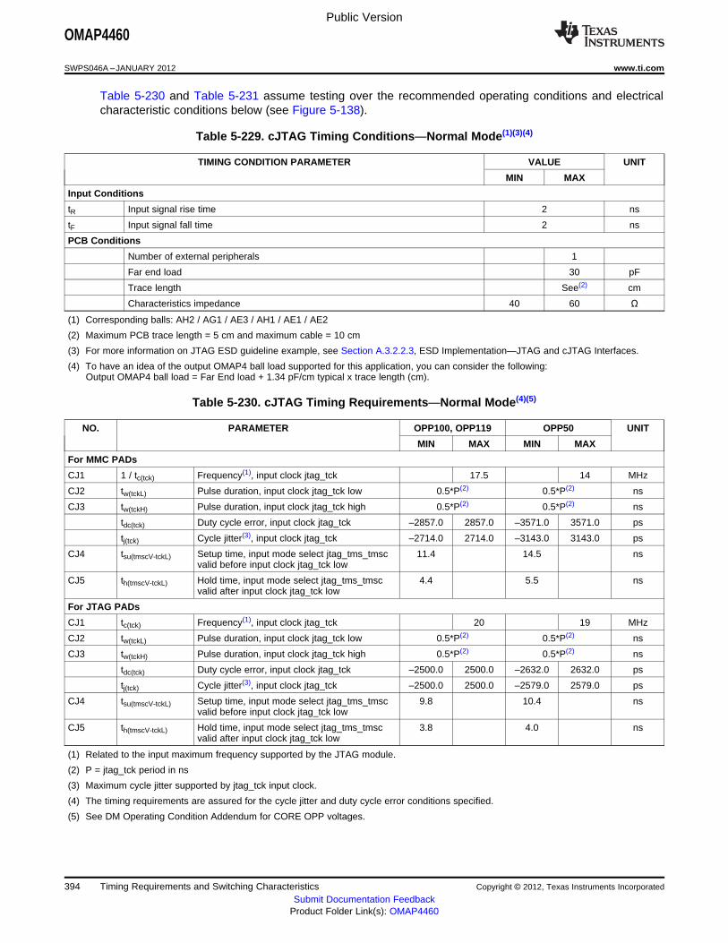
Public Version
OMAP4460
SWPS046A –JANUARY 2012 www.ti.com
Table 5-230 and Table 5-231 assume testing over the recommended operating conditions and electricalcharacteristic conditions below (see Figure 5-138).
Table 5-229. cJTAG Timing Conditions—Normal Mode(1)(3)(4)
TIMING CONDITION PARAMETER VALUE UNIT
MIN MAX
Input Conditions
tR Input signal rise time 2 ns
tF Input signal fall time 2 ns
PCB Conditions
Number of external peripherals 1
Far end load 30 pF
Trace length See(2) cm
Characteristics impedance 40 60 Ω
(1) Corresponding balls: AH2 / AG1 / AE3 / AH1 / AE1 / AE2
(2) Maximum PCB trace length = 5 cm and maximum cable = 10 cm
(3) For more information on JTAG ESD guideline example, see Section A.3.2.2.3, ESD Implementation—JTAG and cJTAG Interfaces.
(4) To have an idea of the output OMAP4 ball load supported for this application, you can consider the following:Output OMAP4 ball load = Far End load + 1.34 pF/cm typical x trace length (cm).
Table 5-230. cJTAG Timing Requirements—Normal Mode(4)(5)
NO. PARAMETER OPP100, OPP119 OPP50 UNIT
MIN MAX MIN MAX
For MMC PADs
CJ1 1 / tc(tck) Frequency(1), input clock jtag_tck 17.5 14 MHz
CJ2 tw(tckL) Pulse duration, input clock jtag_tck low 0.5*P(2) 0.5*P(2) ns
CJ3 tw(tckH) Pulse duration, input clock jtag_tck high 0.5*P(2) 0.5*P(2) ns
tdc(tck) Duty cycle error, input clock jtag_tck –2857.0 2857.0 –3571.0 3571.0 ps
tj(tck) Cycle jitter(3), input clock jtag_tck –2714.0 2714.0 –3143.0 3143.0 ps
CJ4 tsu(tmscV-tckL) Setup time, input mode select jtag_tms_tmsc 11.4 14.5 nsvalid before input clock jtag_tck low
CJ5 th(tmscV-tckL) Hold time, input mode select jtag_tms_tmsc 4.4 5.5 nsvalid after input clock jtag_tck low
For JTAG PADs
CJ1 tc(tck) Frequency(1), input clock jtag_tck 20 19 MHz
CJ2 tw(tckL) Pulse duration, input clock jtag_tck low 0.5*P(2) 0.5*P(2) ns
CJ3 tw(tckH) Pulse duration, input clock jtag_tck high 0.5*P(2) 0.5*P(2) ns
tdc(tck) Duty cycle error, input clock jtag_tck –2500.0 2500.0 –2632.0 2632.0 ps
tj(tck) Cycle jitter(3), input clock jtag_tck –2500.0 2500.0 –2579.0 2579.0 ps
CJ4 tsu(tmscV-tckL) Setup time, input mode select jtag_tms_tmsc 9.8 10.4 nsvalid before input clock jtag_tck low
CJ5 th(tmscV-tckL) Hold time, input mode select jtag_tms_tmsc 3.8 4.0 nsvalid after input clock jtag_tck low
(1) Related to the input maximum frequency supported by the JTAG module.
(2) P = jtag_tck period in ns
(3) Maximum cycle jitter supported by jtag_tck input clock.
(4) The timing requirements are assured for the cycle jitter and duty cycle error conditions specified.
(5) See DM Operating Condition Addendum for CORE OPP voltages.
394 Timing Requirements and Switching Characteristics Copyright © 2012, Texas Instruments Incorporated
Submit Documentation FeedbackProduct Folder Link(s): OMAP4460
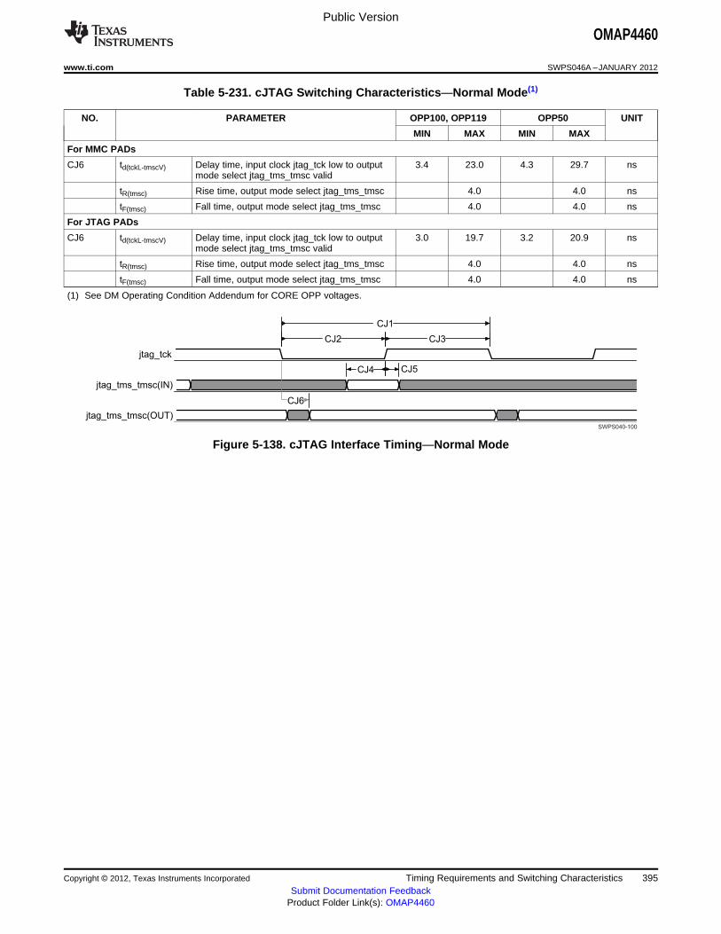
jtag_tck
jtag_tms_tmsc(IN)
jtag_tms_tmsc(OUT)
CJ6
CJ4 CJ5
CJ1
CJ2 CJ3
SWPS040-100
Public Version
OMAP4460
www.ti.com SWPS046A –JANUARY 2012
Table 5-231. cJTAG Switching Characteristics—Normal Mode(1)
NO. PARAMETER OPP100, OPP119 OPP50 UNIT
MIN MAX MIN MAX
For MMC PADs
CJ6 td(tckL-tmscV) Delay time, input clock jtag_tck low to output 3.4 23.0 4.3 29.7 nsmode select jtag_tms_tmsc valid
tR(tmsc) Rise time, output mode select jtag_tms_tmsc 4.0 4.0 ns
tF(tmsc) Fall time, output mode select jtag_tms_tmsc 4.0 4.0 ns
For JTAG PADs
CJ6 td(tckL-tmscV) Delay time, input clock jtag_tck low to output 3.0 19.7 3.2 20.9 nsmode select jtag_tms_tmsc valid
tR(tmsc) Rise time, output mode select jtag_tms_tmsc 4.0 4.0 ns
tF(tmsc) Fall time, output mode select jtag_tms_tmsc 4.0 4.0 ns
(1) See DM Operating Condition Addendum for CORE OPP voltages.
Figure 5-138. cJTAG Interface Timing—Normal Mode
Copyright © 2012, Texas Instruments Incorporated Timing Requirements and Switching Characteristics 395Submit Documentation Feedback
Product Folder Link(s): OMAP4460
Public Version
OMAP4460
SWPS046A –JANUARY 2012 www.ti.com
6 Thermal Management
For reliability and operability concerns, the absolute maximum junction temperature of OMAP4460 has tobe below 125ºC and the maximum average junction temperature has to be below 110ºC.
Depending on the thermal mechanical design (Smartphone, Tablet, Personal Navigation Device, etc), thesystem thermal management software, and worst case thermal applications, the junction temperaturemight be exposed to higher values than those specified above.
Therefore, it is recommended to perform thermal simulations at device level (Smartphone, Tablet,Personal Navigation Device, etc) with the measured power of the worst case UC of the device.
Based on the results, if the temperature limits are exceeded, an OMAP level software thermal policy canbe set up; for detailed information, see the OMAP4460 Thermal Management SWPA188 application note.The OMAP level thermal policy relies on a PCB sensor. Therefore, it is recommended to have suchsensors located on the PCB; for more information, see Section 6.2.1, PCB Sensor Recommendation. Inaddition, it is recommended to avoid having another significant thermal source near the OMAP4460.
The risks of not managing this junction temperature are hazardous heating, power supply clamping,reliability issues, and malfunction.
6.1 Package Thermal Characteristics
Table 6-1 provides the thermal resistance characteristics for the package used on this device.
Table 6-1. Thermal Resistance Characteristics
PACKAGE POWER (W)(4) θJA(ºC/W)(2) ΨJB(ºC/W)(3)(4) BOARD TYPE
OMAP4460 2.6 22.6 9.5 2S2P(1)
(1) The board types are defined by JEDEC (reference JEDEC standard JESD51-9, Test Board for Array Surface Mount Package ThermalMeasurements). Note that the board temperature is measured at 1 mm from the package edge.
(2) ӨJA (Theta-JA) = Thermal Resistance Junction-to-Ambient, °C/W.
(3) ΨJB (Psi-JB) = Thermal Resistance Psi Junction-to-Board, °C/W derived from thermal simulation following JEDEC reference (JEDECstandard JESD51-9, Test Board for Array Surface Mount Package Thermal Measurements).
(4) TJ = P * ΨJB + TBWith P is the dissipated power, TB = 85°C, TJ = 110°C, dissipated power P = 2.6 W.
CAUTION
ΨJB (Psi-JB) value is dependent on the board (PCB) and the power distribution relatedto the power use case: 9.5ºC/W is given for a 2.6-W dissipated power in a JEDEC PCB.Based in ΨJB JEDEC simulation, depending on the device power distribution, the ΨJB
(Psi-JB) could vary between 9ºC/W and 16ºC/W.
396 Thermal Management Copyright © 2012, Texas Instruments Incorporated
Submit Documentation FeedbackProduct Folder Link(s): OMAP4460
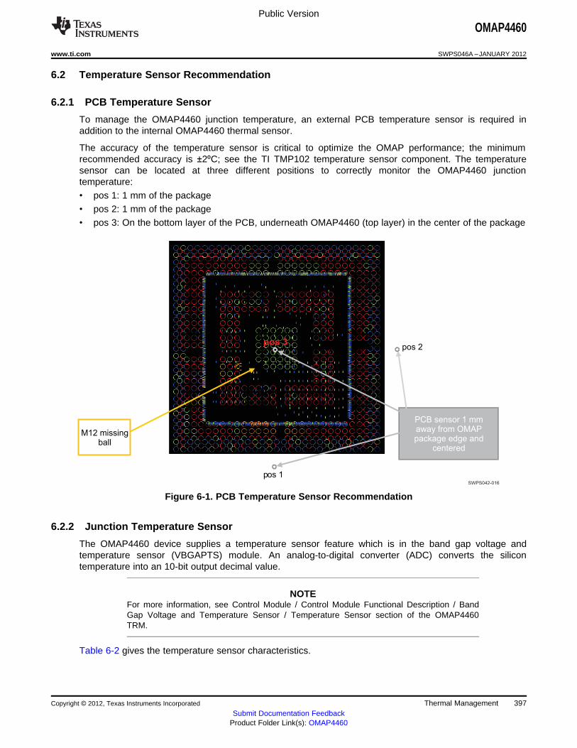
M12 missingball
PCB sensor 1 mmaway from OMAPpackage edge and
centered
pos 1
pos 2pos 3
SWPS042-016
Public Version
OMAP4460
www.ti.com SWPS046A –JANUARY 2012
6.2 Temperature Sensor Recommendation
6.2.1 PCB Temperature Sensor
To manage the OMAP4460 junction temperature, an external PCB temperature sensor is required inaddition to the internal OMAP4460 thermal sensor.
The accuracy of the temperature sensor is critical to optimize the OMAP performance; the minimumrecommended accuracy is ±2ºC; see the TI TMP102 temperature sensor component. The temperaturesensor can be located at three different positions to correctly monitor the OMAP4460 junctiontemperature:• pos 1: 1 mm of the package• pos 2: 1 mm of the package• pos 3: On the bottom layer of the PCB, underneath OMAP4460 (top layer) in the center of the package
Figure 6-1. PCB Temperature Sensor Recommendation
6.2.2 Junction Temperature Sensor
The OMAP4460 device supplies a temperature sensor feature which is in the band gap voltage andtemperature sensor (VBGAPTS) module. An analog-to-digital converter (ADC) converts the silicontemperature into an 10-bit output decimal value.
NOTEFor more information, see Control Module / Control Module Functional Description / BandGap Voltage and Temperature Sensor / Temperature Sensor section of the OMAP4460TRM.
Table 6-2 gives the temperature sensor characteristics.
Copyright © 2012, Texas Instruments Incorporated Thermal Management 397Submit Documentation Feedback
Product Folder Link(s): OMAP4460
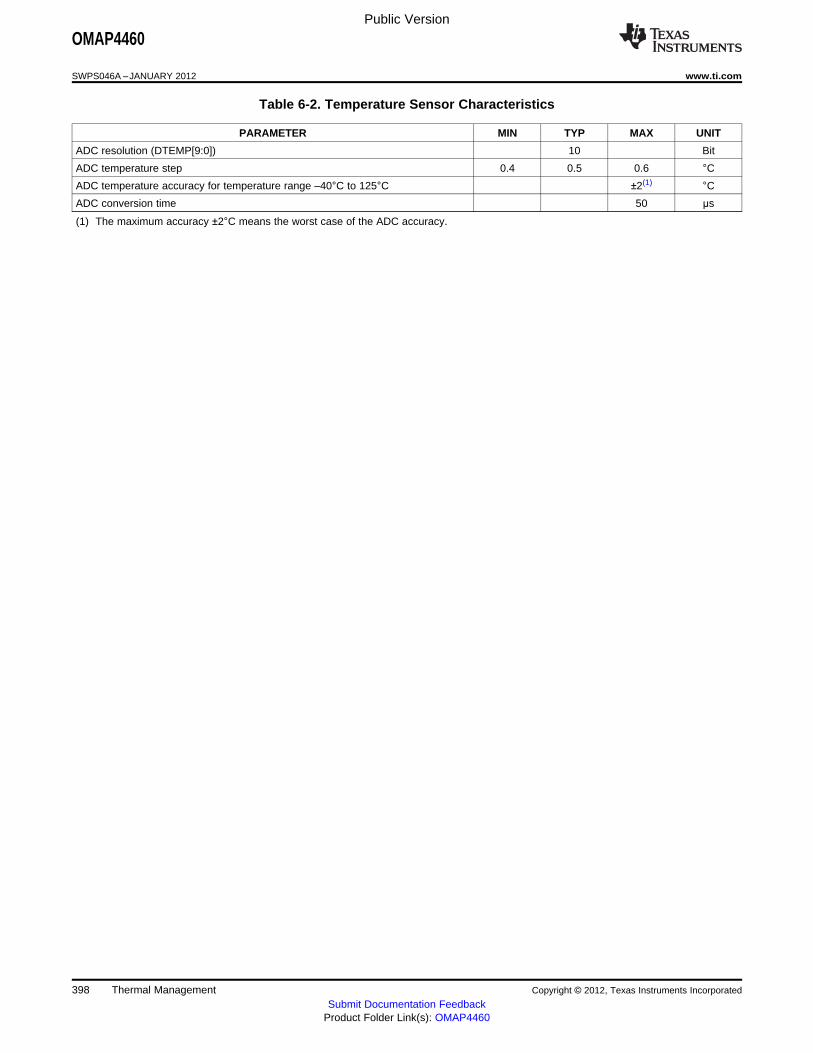
Public Version
OMAP4460
SWPS046A –JANUARY 2012 www.ti.com
Table 6-2. Temperature Sensor Characteristics
PARAMETER MIN TYP MAX UNIT
ADC resolution (DTEMP[9:0]) 10 Bit
ADC temperature step 0.4 0.5 0.6 °CADC temperature accuracy for temperature range –40°C to 125°C ±2(1) °CADC conversion time 50 µs
(1) The maximum accuracy ±2°C means the worst case of the ADC accuracy.
398 Thermal Management Copyright © 2012, Texas Instruments Incorporated
Submit Documentation FeedbackProduct Folder Link(s): OMAP4460

SWPS042-005
OMAP TM
a rPPP4460
Yy
YMLLLL S $PIN ONE DESIGNATOR
O G1
Public Version
OMAP4460
www.ti.com SWPS046A –JANUARY 2012
7 Package Characteristics
7.1 Device Nomenclature
7.1.1 Standard Package Symbolization
Figure 7-1. Printed Device Reference
NOTE• Black: Static field
• Blue: Variable field coded with letters and/or numbers
• Green: Variable fields coded with numbersThe letters and numbers fields are interleaved to facilitate the parameters reading.
Copyright © 2012, Texas Instruments Incorporated Package Characteristics 399Submit Documentation Feedback
Product Folder Link(s): OMAP4460
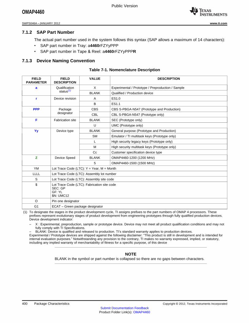
Public Version
OMAP4460
SWPS046A –JANUARY 2012 www.ti.com
7.1.2 SAP Part Number
The actual part number used in the system follows this syntax (SAP allows a maximum of 14 characters):• SAP part number in Tray: a4460rFZYyPPP• SAP part number in Tape & Reel: a4460rFZYyPPPR
7.1.3 Device Naming Convention
Table 7-1. Nomenclature Description
FIELD FIELD VALUE DESCRIPTIONPARAMETER DESCRIPTION
a Qualification X Experimental / Prototype / Preproduction / Samplestatus(1)
BLANK Qualified / Production device
r Device revision A ES1.0
B ES1.1
PPP Package CBS CBS S-PBGA-N547 (Prototype and Production)designator CBL CBL S-PBGA-N547 (Prototype only)
F Fabrication site BLANK SEC (Prototype only)
U UMC (Prototype only)
Yy Device type BLANK General purpose (Prototype and Production)
SM Emulator / TI multitask keys (Prototype only)
L High security legacy keys (Prototype only)
M High security multitask keys (Prototype only)
Cc Customer specification device type
Z Device Speed BLANK OMAP4460-1200 (1200 MHz)
5 OMAP4460-1500 (1500 MHz)
YM Lot Trace Code (LTC): Y = Year, M = Month
LLLL Lot Trace Code (LTC): Assembly lot number
S Lot Trace Code (LTC): Assembly site code
$ Lot Trace Code (LTC): Fabrication site codeSEC: GPGF: YL$N: UMC12
O Pin one designator
G1 ECAT – Green package designator
(1) To designate the stages in the product development cycle, TI assigns prefixes to the part numbers of OMAP 4 processors. Theseprefixes represent evolutionary stages of product development from engineering prototypes through fully qualified production devices.Device development indicator:
– X : Experimental, preproduction, sample or prototype device. Device may not meet all product qualification conditions and may notfully comply with TI Specifications.
– BLANK: Device is qualified and released to production. TI’s standard warranty applies to production devices.Experimental / Prototype devices are shipped against the following disclaimer: “This product is still in development and is intended forinternal evaluation purposes.” Notwithstanding any provision to the contrary, TI makes no warranty expressed, implied, or statutory,including any implied warranty of merchantability of fitness for a specific purpose, of this device
NOTEBLANK in the symbol or part number is collapsed so there are no gaps between characters.
400 Package Characteristics Copyright © 2012, Texas Instruments Incorporated
Submit Documentation FeedbackProduct Folder Link(s): OMAP4460
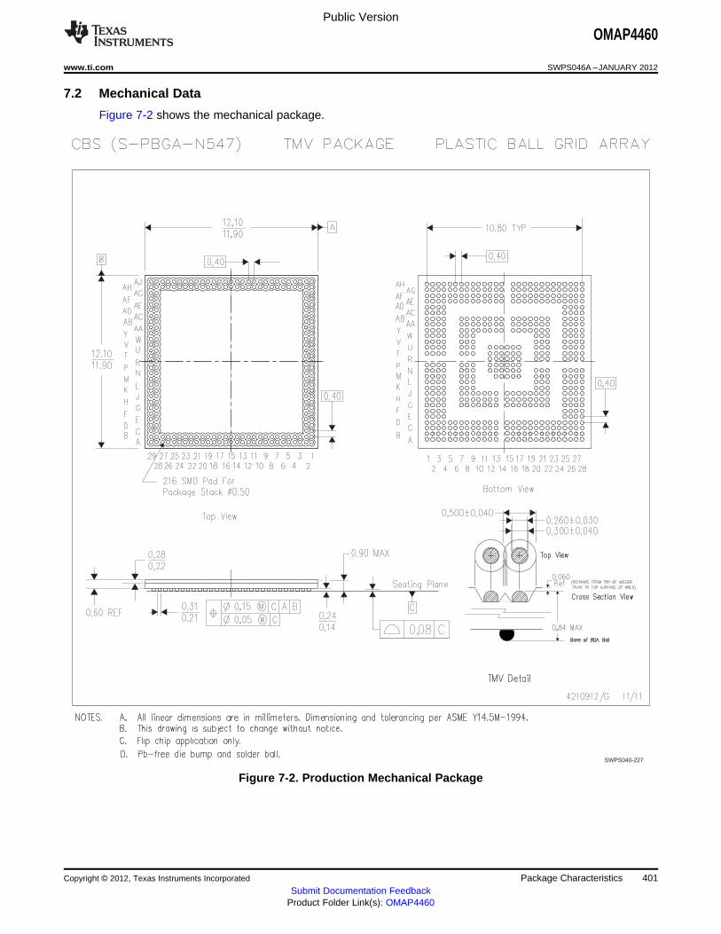
SWPS040-227
Public Version
OMAP4460
www.ti.com SWPS046A –JANUARY 2012
7.2 Mechanical Data
Figure 7-2 shows the mechanical package.
Figure 7-2. Production Mechanical Package
Copyright © 2012, Texas Instruments Incorporated Package Characteristics 401Submit Documentation Feedback
Product Folder Link(s): OMAP4460
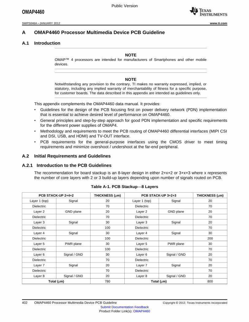
Public Version
OMAP4460
SWPS046A –JANUARY 2012 www.ti.com
A OMAP4460 Processor Multimedia Device PCB Guideline
A.1 Introduction
NOTEOMAP™ 4 processors are intended for manufacturers of Smartphones and other mobiledevices.
NOTENotwithstanding any provision to the contrary, TI makes no warranty expressed, implied, orstatutory, including any implied warranty of merchantability of fitness for a specific purpose,for customer boards. The data described in this appendix are intended as guidelines only.
This appendix complements the OMAP4460 data manual. It provides:• Guidelines for the design of the PCB focusing first on power delivery network (PDN) implementation
that is essential to achieve desired level of performance on OMAP4460.• General principles and step-by-step approach for good PDN implementation and specific requirements
for the different power supplies of OMAP4.• Methodology and requirements to meet the PCB routing of OMAP4460 differential interfaces (MIPI CSI
and DSI, USB, and HDMI) and TV-OUT interface.• PCB requirements for the general-purpose interfaces using the CMOS driver to meet timing
requirements and minimize overshoot / undershoot at the far-end peripheral.
A.2 Initial Requirements and Guidelines
A.2.1 Introduction to the PCB Guidelines
The recommendation for board stackup is an 8-layer design in either 2+x+2 or 3+x+3 where x representsthe number of core layers with 2 or 3 build-up layers depending upon number of signals routed on PCB.
Table A-1. PCB Stackup—8 Layers
PCB STACK-UP 2+4+2 THICKNESS (µm) PCB STACK-UP 3+2+3 THICKNESS (µm)
Layer 1 (top) Signal 20 Layer 1 (top) Signal 20
Dielectric 70 Dielectric 70
Layer 2 GND plane 20 Layer 2 GND plane 20
Dielectric 70 Dielectric 70
Layer 3 Signal 30 Layer 3 Signal 20
Dielectric 100 Dielectric 70
Layer 4 Signal 30 Layer 4 Signal 30
Dielectric 100 Dielectric 200
Layer 5 PWR plane 30 Layer 5 PWR plane 30
Dielectric 100 Dielectric 70
Layer 6 Signal / GND 30 Layer 6 Signal / GND 20
Dielectric 70 Dielectric 70
Layer 7 Signal 20 Layer 7 Signal 20
Dielectric 70 Dielectric 70
Layer 8 Signal / GND 20 Layer 8 Signal / GND 20
Total (µm) 780 Total (µm) 800
402 OMAP4460 Processor Multimedia Device PCB Guideline Copyright © 2012, Texas Instruments Incorporated
Submit Documentation FeedbackProduct Folder Link(s): OMAP4460
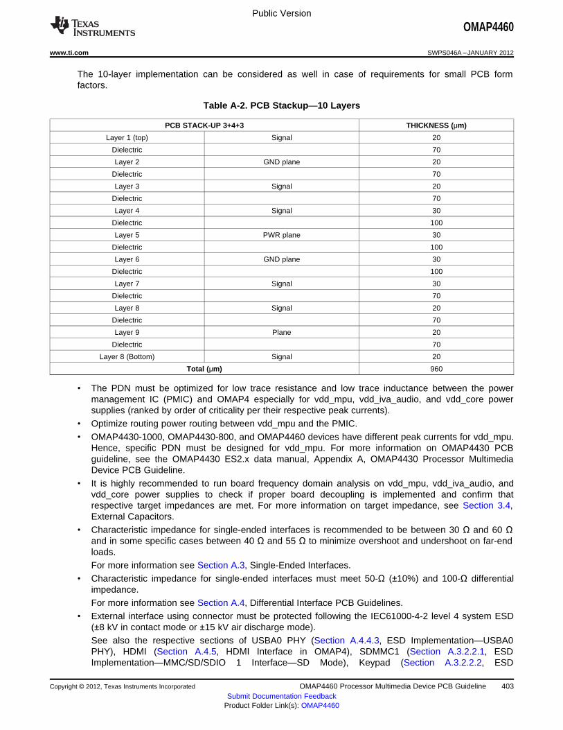
Public Version
OMAP4460
www.ti.com SWPS046A –JANUARY 2012
The 10-layer implementation can be considered as well in case of requirements for small PCB formfactors.
Table A-2. PCB Stackup—10 Layers
PCB STACK-UP 3+4+3 THICKNESS (µm)
Layer 1 (top) Signal 20
Dielectric 70
Layer 2 GND plane 20
Dielectric 70
Layer 3 Signal 20
Dielectric 70
Layer 4 Signal 30
Dielectric 100
Layer 5 PWR plane 30
Dielectric 100
Layer 6 GND plane 30
Dielectric 100
Layer 7 Signal 30
Dielectric 70
Layer 8 Signal 20
Dielectric 70
Layer 9 Plane 20
Dielectric 70
Layer 8 (Bottom) Signal 20
Total (µm) 960
• The PDN must be optimized for low trace resistance and low trace inductance between the powermanagement IC (PMIC) and OMAP4 especially for vdd_mpu, vdd_iva_audio, and vdd_core powersupplies (ranked by order of criticality per their respective peak currents).
• Optimize routing power routing between vdd_mpu and the PMIC.• OMAP4430-1000, OMAP4430-800, and OMAP4460 devices have different peak currents for vdd_mpu.
Hence, specific PDN must be designed for vdd_mpu. For more information on OMAP4430 PCBguideline, see the OMAP4430 ES2.x data manual, Appendix A, OMAP4430 Processor MultimediaDevice PCB Guideline.
• It is highly recommended to run board frequency domain analysis on vdd_mpu, vdd_iva_audio, andvdd_core power supplies to check if proper board decoupling is implemented and confirm thatrespective target impedances are met. For more information on target impedance, see Section 3.4,External Capacitors.
• Characteristic impedance for single-ended interfaces is recommended to be between 30 Ω and 60 Ωand in some specific cases between 40 Ω and 55 Ω to minimize overshoot and undershoot on far-endloads.For more information see Section A.3, Single-Ended Interfaces.
• Characteristic impedance for single-ended interfaces must meet 50-Ω (±10%) and 100-Ω differentialimpedance.For more information see Section A.4, Differential Interface PCB Guidelines.
• External interface using connector must be protected following the IEC61000-4-2 level 4 system ESD(±8 kV in contact mode or ±15 kV air discharge mode).See also the respective sections of USBA0 PHY (Section A.4.4.3, ESD Implementation—USBA0PHY), HDMI (Section A.4.5, HDMI Interface in OMAP4), SDMMC1 (Section A.3.2.2.1, ESDImplementation—MMC/SD/SDIO 1 Interface—SD Mode), Keypad (Section A.3.2.2.2, ESD
Copyright © 2012, Texas Instruments Incorporated OMAP4460 Processor Multimedia Device PCB Guideline 403Submit Documentation Feedback
Product Folder Link(s): OMAP4460

OMAP Package
OMAP DIE
TraceCapacitor
Via
Note: 1. BGA via pair loop inductance
2. Power/Ground net spreading inductance
3. Capacitor trace inductance
Loop inductance
1
2
3
Power/Ground
Ground/Power
SWPS040-167
Public Version
OMAP4460
SWPS046A –JANUARY 2012 www.ti.com
Implementation—KeyPAD Interface) and JTAG or cJTAG (Section A.3.2.2.3, ESDImplementation—JTAG and cJTAG Interfaces) interfaces for specific ESD requirements andimplementation proposals.
• LPDDR2 memory:– OMAP4 supports two LPDDR2 channels. Each of these channels supports up to two chip selects.
Up to four LPDDR2 memory dies can be connected on top of OMAP4 package viaPackage-on-Package implementation. Powers for LPDDR2 memory are connected via feedthroughin OMAP4460 package.
– The memory component LPDDR2-S4A and LPDDR2-S4B memory have different voltagerequirements. The S4B type needs a single 1.2-V source to supply vdd2 and vddq / vddca.
A.2.2 PCB Power General Routing Guidelines
In this section you will find the necessary steps for the PCB power general routing:• Section A.2.2.1, Step 1: Requirements and guidelines for PCB stack-up• Section A.2.2.2, Step 2: Physical layout guidelines of the PDN• Section A.2.2.3, Step 3: Static IR drop guidelines of PDN. Minimize resistance, avoid neck-down, and
reduce current density.
A.2.2.1 Step 1: PCB Stack-up Guidelines
The PCB stack-up (layer assignment) is an important factor in determining the optimal performance of thepower distribution system. An optimized PCB stack-up for higher power integrity performance can beachieved by following these requirements:• Power and ground plane pairs must be closely coupled together. The capacitance formed between the
planes can decouple the power supply at high frequencies. Whenever possible, the power and theground planes must be solid to provide continuous return path for return current.
• Use a thin dielectric thickness between the power and ground plane pair. Capacitance is inverselyproportional to the separation of the plane pair. Minimizing the separation distance (the dielectricthickness) will maximize the capacitance.
• Keep the power and ground plane pair as close as possible to the top and bottom surfaces (seeFigure A-1). This will help in minimizing the decoupling capacitors mounting, via, and the power /ground plane pair spreading loop inductance.
Figure A-1. Minimize Loop Inductance With Proper Layer Assignment
The placement of power and ground planes in the PCB stackup (determined by layer assignment) has a
404 OMAP4460 Processor Multimedia Device PCB Guideline Copyright © 2012, Texas Instruments Incorporated
Submit Documentation FeedbackProduct Folder Link(s): OMAP4460
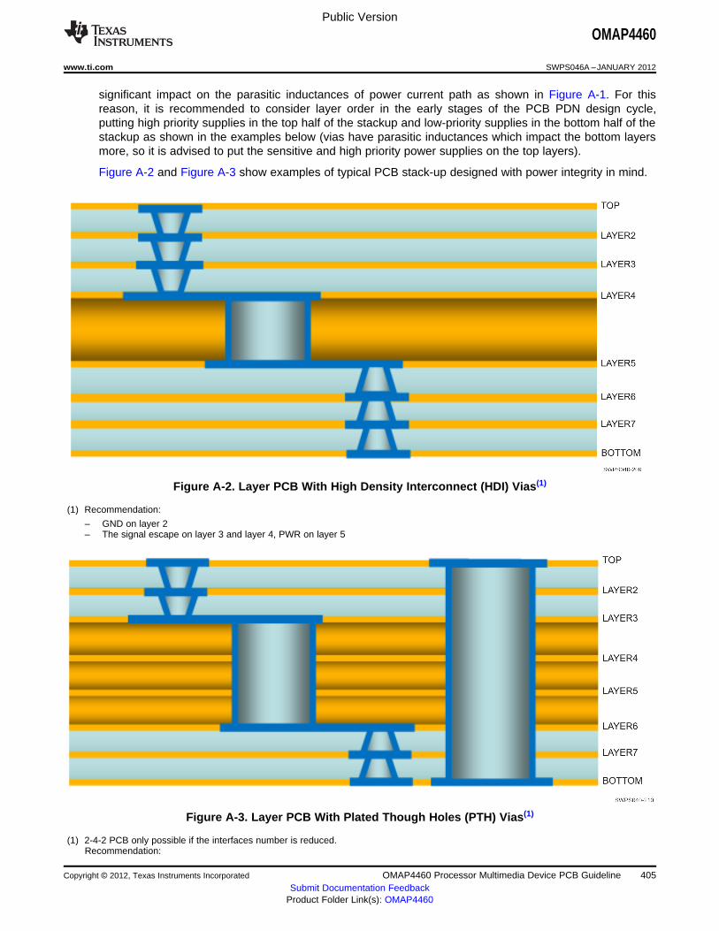
Public Version
OMAP4460
www.ti.com SWPS046A –JANUARY 2012
significant impact on the parasitic inductances of power current path as shown in Figure A-1. For thisreason, it is recommended to consider layer order in the early stages of the PCB PDN design cycle,putting high priority supplies in the top half of the stackup and low-priority supplies in the bottom half of thestackup as shown in the examples below (vias have parasitic inductances which impact the bottom layersmore, so it is advised to put the sensitive and high priority power supplies on the top layers).
Figure A-2 and Figure A-3 show examples of typical PCB stack-up designed with power integrity in mind.
Figure A-2. Layer PCB With High Density Interconnect (HDI) Vias(1)
(1) Recommendation:
– GND on layer 2– The signal escape on layer 3 and layer 4, PWR on layer 5
Figure A-3. Layer PCB With Plated Though Holes (PTH) Vias(1)
(1) 2-4-2 PCB only possible if the interfaces number is reduced.Recommendation:
Copyright © 2012, Texas Instruments Incorporated OMAP4460 Processor Multimedia Device PCB Guideline 405Submit Documentation Feedback
Product Folder Link(s): OMAP4460

Public Version
OMAP4460
SWPS046A –JANUARY 2012 www.ti.com
– GND on layer 2– Signal escape on layer 3 and layer 4, PWR on layer 5
A.2.2.2 Step 2: Physical Layout Guidelines of the PDN
A critical step in designing an optimized PDN is that proper care must be taken to ensure that the initiallayout is planned with good power integrity design guidelines in mind. The following points are importantrequirements that will be needed to be implemented in the PCB PDN design:• External trace routing between components must be as wide as possible. The wider the traces the
lower the dc resistance and consequently the lower the static IR drop.• Whenever possible, try aiming for a ratio of 1:1 or better for component (for example, capacitors and
resistors) pins and vias. Do not share vias among multiple capacitors.• Placement of the vias must be as close as possible to the solder pad.
Figure A-4 shows an example of acceptable width for power net routing but with poor via placement.
Figure A-4. Poor Via Assignment for PDN
Figure A-5 shows an improved power net routing with appropriate via assignment and placement.
406 OMAP4460 Processor Multimedia Device PCB Guideline Copyright © 2012, Texas Instruments Incorporated
Submit Documentation FeedbackProduct Folder Link(s): OMAP4460

Public Version
OMAP4460
www.ti.com SWPS046A –JANUARY 2012
Figure A-5. Improved Via Assignment for PDN
• To avoid the maximum current carrying capacity of each transitional via, an evaluation must beperformed to determine the appropriate number of vias required to connect components.Figure A-6 and Figure A-7 show examples of via starvation on a power net transitioning from toprouting layer to internal layers and the improved layout, respectively.
Figure A-6. Via Starvation
Copyright © 2012, Texas Instruments Incorporated OMAP4460 Processor Multimedia Device PCB Guideline 407Submit Documentation Feedback
Product Folder Link(s): OMAP4460

Public Version
OMAP4460
SWPS046A –JANUARY 2012 www.ti.com
Figure A-7. Improved Layout With More Transitional Vias
• It is also a good practice to perform static IR drop. This analysis can assess the appropriate number ofvias and geometrical trace width dimensions required for the expected IR drop requirement.
• Whenever possible for the internal layers (routing and plane), wide traces and copper area fills arepreferred for the PDN layout. The routing power nets in plane provide for more interplane capacitanceand improve high frequency performance of the PDN.
• Try to avoid different power nets (for example, VDD_MPU with VDD_CORE) coupling on the PCB byusing coplanar shielding whenever appropriate.Figure A-8 represents an example of coplanar shielding for power nets.
Figure A-8. Coplanar Shielding of Power Net Using Ground Guard-band
• Decoupling capacitors must be mounted with minimum impact to inductance. A real capacitor hascharacteristics not only of capacitance but also inductance and resistance.Figure A-9 shows the parasitic model of a real capacitor. A real capacitor must be treated as an RLCcircuit with effective series resistance (ESR) and effective series inductance (ESL).
408 OMAP4460 Processor Multimedia Device PCB Guideline Copyright © 2012, Texas Instruments Incorporated
Submit Documentation FeedbackProduct Folder Link(s): OMAP4460

C ESL ESRSWPS040-175
=
where :
æ ö-ç ÷
è ø
w =
2
2 1Z ESR +ωESL
ωC
2π
æ ö-ç ÷
è ø
21
ωESLωC
SWPS040-e002
¦
SWPS040-176
1.0e+01
1.0e+00
1.0e–01
1.0e–02
1.0e–03
1.0e–041.00e–002 1.00e+000 1.00e+002
Frequency (MHz)
1.00e+004 1.00e+006 1.00e+008
S-Parameter Magnitude
Job: GCM155R71E153KA55_15NF;
X =1/ CC ω X = LL ω
Resonant frequency(55 MHz) (minimum)
Public Version
OMAP4460
www.ti.com SWPS046A –JANUARY 2012
Figure A-9. Characteristics of a Real Capacitor With ESL and ESR
The magnitude of the impedance of this series model is given as:
Figure A-10. Series Model Impedance Equation
Figure A-11 shows the resonant frequency response of a typical capacitor with self-resonant frequency of55 MHz. The impedance of the capacitor is a combination of its series resistance and reactive capacitanceand inductance as shown in the equation above.
Figure A-11. Typical Impedance Profile of a Capacitor
Because a capacitor has series inductance and resistance that will impact its effectiveness, it is importantthat the following recommendations are adopted in placing them on the PDN. Whenever possible, pleasemount the capacitor with the geometry that will minimize the mounting inductance and resistance. Thiswas shown earlier in Figure A-1. The capacitor mounting inductance and resistance includes theinductance and resistance of the pads, trace, and vias.
Copyright © 2012, Texas Instruments Incorporated OMAP4460 Processor Multimedia Device PCB Guideline 409Submit Documentation Feedback
Product Folder Link(s): OMAP4460
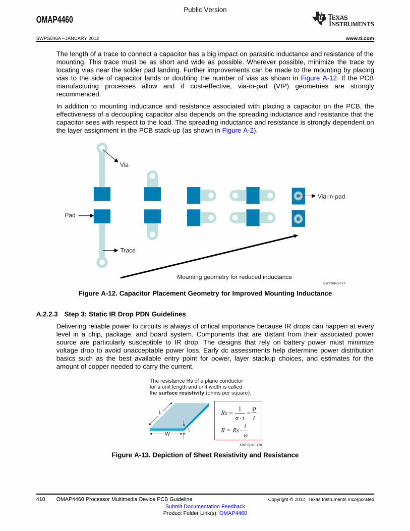
Trace
Pad
Via
Mounting geometry for reduced inductance
Via-in-pad
SWPS040-177
L
Wt
The resistance Rs of a plane conductorfor a unit length and unit width is calledthe (ohms per square).surface resistivity
1
σ ×
×
Rs = =t
lR = Rs
w
rt
SWPS040-178
Public Version
OMAP4460
SWPS046A –JANUARY 2012 www.ti.com
The length of a trace to connect a capacitor has a big impact on parasitic inductance and resistance of themounting. This trace must be as short and wide as possible. Wherever possible, minimize the trace bylocating vias near the solder pad landing. Further improvements can be made to the mounting by placingvias to the side of capacitor lands or doubling the number of vias as shown in Figure A-12. If the PCBmanufacturing processes allow and if cost-effective, via-in-pad (VIP) geometries are stronglyrecommended.
In addition to mounting inductance and resistance associated with placing a capacitor on the PCB, theeffectiveness of a decoupling capacitor also depends on the spreading inductance and resistance that thecapacitor sees with respect to the load. The spreading inductance and resistance is strongly dependent onthe layer assignment in the PCB stack-up (as shown in Figure A-2).
Figure A-12. Capacitor Placement Geometry for Improved Mounting Inductance
A.2.2.3 Step 3: Static IR Drop PDN Guidelines
Delivering reliable power to circuits is always of critical importance because IR drops can happen at everylevel in a chip, package, and board system. Components that are distant from their associated powersource are particularly susceptible to IR drop. The designs that rely on battery power must minimizevoltage drop to avoid unacceptable power loss. Early dc assessments help determine power distributionbasics such as the best available entry point for power, layer stackup choices, and estimates for theamount of copper needed to carry the current.
Figure A-13. Depiction of Sheet Resistivity and Resistance
410 OMAP4460 Processor Multimedia Device PCB Guideline Copyright © 2012, Texas Instruments Incorporated
Submit Documentation FeedbackProduct Folder Link(s): OMAP4460
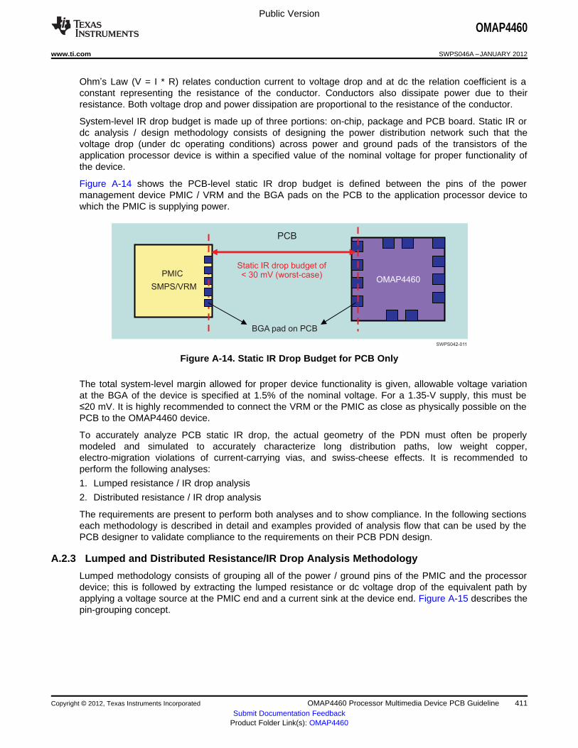
PMIC
SMPS/VRMOMAP4460
PCB
Static IR drop budget of< 30 mV (worst-case)
BGA pad on PCB
SWPS042-011
Public Version
OMAP4460
www.ti.com SWPS046A –JANUARY 2012
Ohm’s Law (V = I * R) relates conduction current to voltage drop and at dc the relation coefficient is aconstant representing the resistance of the conductor. Conductors also dissipate power due to theirresistance. Both voltage drop and power dissipation are proportional to the resistance of the conductor.
System-level IR drop budget is made up of three portions: on-chip, package and PCB board. Static IR ordc analysis / design methodology consists of designing the power distribution network such that thevoltage drop (under dc operating conditions) across power and ground pads of the transistors of theapplication processor device is within a specified value of the nominal voltage for proper functionality ofthe device.
Figure A-14 shows the PCB-level static IR drop budget is defined between the pins of the powermanagement device PMIC / VRM and the BGA pads on the PCB to the application processor device towhich the PMIC is supplying power.
Figure A-14. Static IR Drop Budget for PCB Only
The total system-level margin allowed for proper device functionality is given, allowable voltage variationat the BGA of the device is specified at 1.5% of the nominal voltage. For a 1.35-V supply, this must be≤20 mV. It is highly recommended to connect the VRM or the PMIC as close as physically possible on thePCB to the OMAP4460 device.
To accurately analyze PCB static IR drop, the actual geometry of the PDN must often be properlymodeled and simulated to accurately characterize long distribution paths, low weight copper,electro-migration violations of current-carrying vias, and swiss-cheese effects. It is recommended toperform the following analyses:
1. Lumped resistance / IR drop analysis
2. Distributed resistance / IR drop analysis
The requirements are present to perform both analyses and to show compliance. In the following sectionseach methodology is described in detail and examples provided of analysis flow that can be used by thePCB designer to validate compliance to the requirements on their PCB PDN design.
A.2.3 Lumped and Distributed Resistance/IR Drop Analysis Methodology
Lumped methodology consists of grouping all of the power / ground pins of the PMIC and the processordevice; this is followed by extracting the lumped resistance or dc voltage drop of the equivalent path byapplying a voltage source at the PMIC end and a current sink at the device end. Figure A-15 describes thepin-grouping concept.
Copyright © 2012, Texas Instruments Incorporated OMAP4460 Processor Multimedia Device PCB Guideline 411Submit Documentation Feedback
Product Folder Link(s): OMAP4460

Grouped Power/Groundpins to create 1 equivalent
resistive branch
Multiport net
Branch
Port/Pin
Sources
Sinks
Sources
Sinks
SWPS040-179
Public Version
OMAP4460
SWPS046A –JANUARY 2012 www.ti.com
Figure A-15. Pin-grouping Concept: Lumped and Distributed Methodologies
The lumped methodology consists of importing the PCB layout database (from Cadence Allegro tool orany other layout design tool) into the static IR drop modeling and simulation tool of preference for the PCBdesigner. This is followed by applying the correct PCB stack-up information (thickness, materialproperties) of the PCB dielectric and metallization layers. The material properties of dielectric consist ofpermittivity (Dk) and loss tangent (Df).
For the conductor layers, the correct conductivity needs to be programmed into the simulation tool. This isfollowed by pin-grouping of the power and ground nets, and applying appropriate voltage / currentsources.
The current and voltage information can be obtained from the power and voltage specifications of thedevice under different operating conditions / use-modes. After running the simulation, the lumpedresistance and lumped IR drop can be examined as shown in Figure A-15.
A.2.4 System ESD Generic Guidelines
NOTEIEC61000-4-2: The ESD discharges described in this section apply only to HDMI, USBA0PHY, SD/MMC card cage, composite video, JTAG, cJTAG, and points and surfaces of theEquipment Under Test (EUT) that are accessible to the end-user during normal use.
The following exclusions apply (that is, discharges are not applied to these items):• In the case of the contacts of coaxial and multipin connectors which are provided with a metallic
connector shell, contact discharges are only applied to the metallic shell contacts. Falling into thiscategory:HDMI/USB connectors, SD/MMC card cage, audio headset jack connector
• Those points and surfaces that are only accessible under service by the end-user. Examples of theserarely accessed points are battery contacts while changing batteries. Falling into this category:Battery connector
• Those points and surfaces that are only accessible under maintenance. In this case, special ESDmitigation procedures are given in the accompanying documentation. Falling into this category:JTAG test points
• Those points and surfaces of equipment that are no longer accessible after fixed installation or afterfollowing the instructions for use; for example, the bottom and/or wall side of equipment or areasbehind fitted connectors. Potentially falling into this category:Audio speaker spring contacts
A.2.4.1 IEC61000-4-2 Standard Overview—System ESD
System ESD differs from the usual component level ESD tests such as HBM (ANSI/ESDA/JEDECJS-001-2010) or CDM (JESD22 C101) described in Table 3-1, Absolute Maximum Rating Over Junction
412 OMAP4460 Processor Multimedia Device PCB Guideline Copyright © 2012, Texas Instruments Incorporated
Submit Documentation FeedbackProduct Folder Link(s): OMAP4460
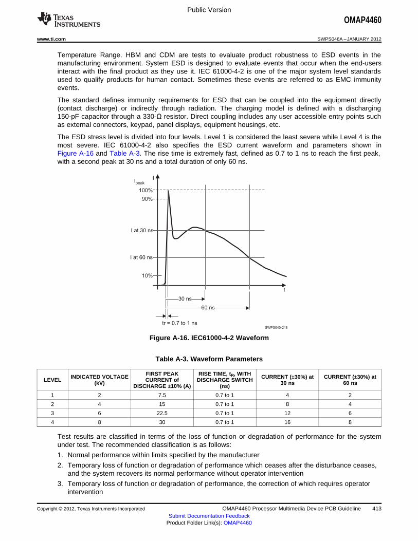
Ipeak
100%
90%
I at 30 ns
I at 60 ns
10%
t
tr = 0.7 to 1 ns
I
30 ns
60 ns
SWPS040-218
Public Version
OMAP4460
www.ti.com SWPS046A –JANUARY 2012
Temperature Range. HBM and CDM are tests to evaluate product robustness to ESD events in themanufacturing environment. System ESD is designed to evaluate events that occur when the end-usersinteract with the final product as they use it. IEC 61000-4-2 is one of the major system level standardsused to qualify products for human contact. Sometimes these events are referred to as EMC immunityevents.
The standard defines immunity requirements for ESD that can be coupled into the equipment directly(contact discharge) or indirectly through radiation. The charging model is defined with a discharging150-pF capacitor through a 330-Ω resistor. Direct coupling includes any user accessible entry points suchas external connectors, keypad, panel displays, equipment housings, etc.
The ESD stress level is divided into four levels. Level 1 is considered the least severe while Level 4 is themost severe. IEC 61000-4-2 also specifies the ESD current waveform and parameters shown inFigure A-16 and Table A-3. The rise time is extremely fast, defined as 0.7 to 1 ns to reach the first peak,with a second peak at 30 ns and a total duration of only 60 ns.
Figure A-16. IEC61000-4-2 Waveform
Table A-3. Waveform Parameters
FIRST PEAK RISE TIME, tR, WITHINDICATED VOLTAGE CURRENT (±30%) at CURRENT (±30%) atLEVEL CURRENT of DISCHARGE SWITCH(kV) 30 ns 60 nsDISCHARGE ±10% (A) (ns)
1 2 7.5 0.7 to 1 4 2
2 4 15 0.7 to 1 8 4
3 6 22.5 0.7 to 1 12 6
4 8 30 0.7 to 1 16 8
Test results are classified in terms of the loss of function or degradation of performance for the systemunder test. The recommended classification is as follows:
1. Normal performance within limits specified by the manufacturer
2. Temporary loss of function or degradation of performance which ceases after the disturbance ceases,and the system recovers its normal performance without operator intervention
3. Temporary loss of function or degradation of performance, the correction of which requires operatorintervention
Copyright © 2012, Texas Instruments Incorporated OMAP4460 Processor Multimedia Device PCB Guideline 413Submit Documentation Feedback
Product Folder Link(s): OMAP4460
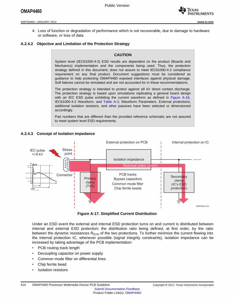
100%
90%
I at 30 ns
I at 60 ns
10%
t
tr = 0.7 to 1 ns
30 ns
60 ns
30 A
IEC pulse+/-8 kV
Stresspoint
Connector
External protection on PCB Internal protection on IC
PCB tracks
Bypass capacitors
Common mode filter
Chip ferrite beads
Isolation impedance
SWPS040-219
Primaryclamp(TVS)
Secondaryclamp
(IC’s ESDprotection)
Residual pulse current
Public Version
OMAP4460
SWPS046A –JANUARY 2012 www.ti.com
4. Loss of function or degradation of performance which is not recoverable, due to damage to hardwareor software, or loss of data
A.2.4.2 Objective and Limitation of the Protection Strategy
CAUTION
System level (IEC61000-4-2) ESD results are dependent on the product (Boards andMechanics) implementation and the components being used. Thus, the protectionstrategy defined in this document, does not assure to meet IEC61000-4-2 compliancerequirement on any final product. Document suggestions must be considered asguidance to help protecting OMAP4460 exposed interfaces against physical damage.Soft failures cannot be simulated and are not accounted for in these recommendations.
The protection strategy is intended to protect against ±8 kV direct contact discharge.The protection strategy is based upon simulations replicating a general board designwith an IEC ESD pulse exhibiting the current waveform as defined in Figure A-16,IEC61000-4-2 Waveform, and Table A-3, Waveform Parameters. External protections,additional isolation resistors, and other passives have been selected or dimensionedaccordingly.
Part numbers that are different than the provided reference schematic are not assuredto meet system level ESD requirements.
A.2.4.3 Concept of Isolation Impedance
Figure A-17. Simplified Current Distribution
Under an ESD event the external and internal ESD protection turns on and current is distributed betweeninternal and external ESD protection; the distribution ratio being defined, at first order, by the ratiobetween the dynamic resistances RDYN of the two protections. To further minimize the current flowing intothe internal protection IC, whenever possible (signal integrity constraints), isolation impedance can beincreased by taking advantage of the PCB implementation:• PCB routing track length• Decoupling capacitor on power supply• Common mode filter on differential lines• Chip ferrite bead• Isolation resistors
414 OMAP4460 Processor Multimedia Device PCB Guideline Copyright © 2012, Texas Instruments Incorporated
Submit Documentation FeedbackProduct Folder Link(s): OMAP4460
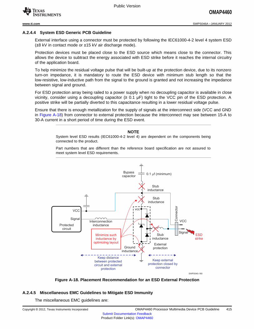
Minimize suchinductance by
optimizing layout
Keep distancebetween protectedcircuit and external
protection
Keepprotection closed by
connector
external
Externalprotection
Stubinductance
Groundinductance
SignalESDstrike
VCCConnecto
r
Stubinductance
Stubinductance
Bypasscapacitor
0.1 f (minimum)m
Interconnectioninductance
vccVCC
Signal
Protectedcircuit
SWPS040-180
Public Version
OMAP4460
www.ti.com SWPS046A –JANUARY 2012
A.2.4.4 System ESD Generic PCB Guideline
External interface using a connector must be protected by following the IEC61000-4-2 level 4 system ESD(±8 kV in contact mode or ±15 kV air discharge mode).
Protection devices must be placed close to the ESD source which means close to the connector. Thisallows the device to subtract the energy associated with ESD strike before it reaches the internal circuitryof the application board.
To help minimize the residual voltage pulse that will be built-up at the protection device, due to its nonzeroturn-on impedance, it is mandatory to route the ESD device with minimum stub length so that thelow-resistive, low-inductive path from the signal to the ground is granted and not increasing the impedancebetween signal and ground.
For ESD protection array being railed to a power supply when no decoupling capacitor is available in closevicinity, consider using a decoupling capacitor (≥ 0.1 µF) tight to the VCC pin of the ESD protection. Apositive strike will be partially diverted to this capacitance resulting in a lower residual voltage pulse.
Ensure that there is enough metallization for the supply of signals at the interconnect side (VCC and GNDin Figure A-18) from connector to external protection because the interconnect may see between 15-A to30-A current in a short period of time during the ESD event.
NOTESystem level ESD results (IEC61000-4-2 level 4) are dependent on the components beingconnected to the product.
Part numbers that are different than the reference board specification are not assured tomeet system level ESD requirements.
Figure A-18. Placement Recommendation for an ESD External Protection
A.2.4.5 Miscellaneous EMC Guidelines to Mitigate ESD Immunity
The miscellaneous EMC guidelines are:
Copyright © 2012, Texas Instruments Incorporated OMAP4460 Processor Multimedia Device PCB Guideline 415Submit Documentation Feedback
Product Folder Link(s): OMAP4460
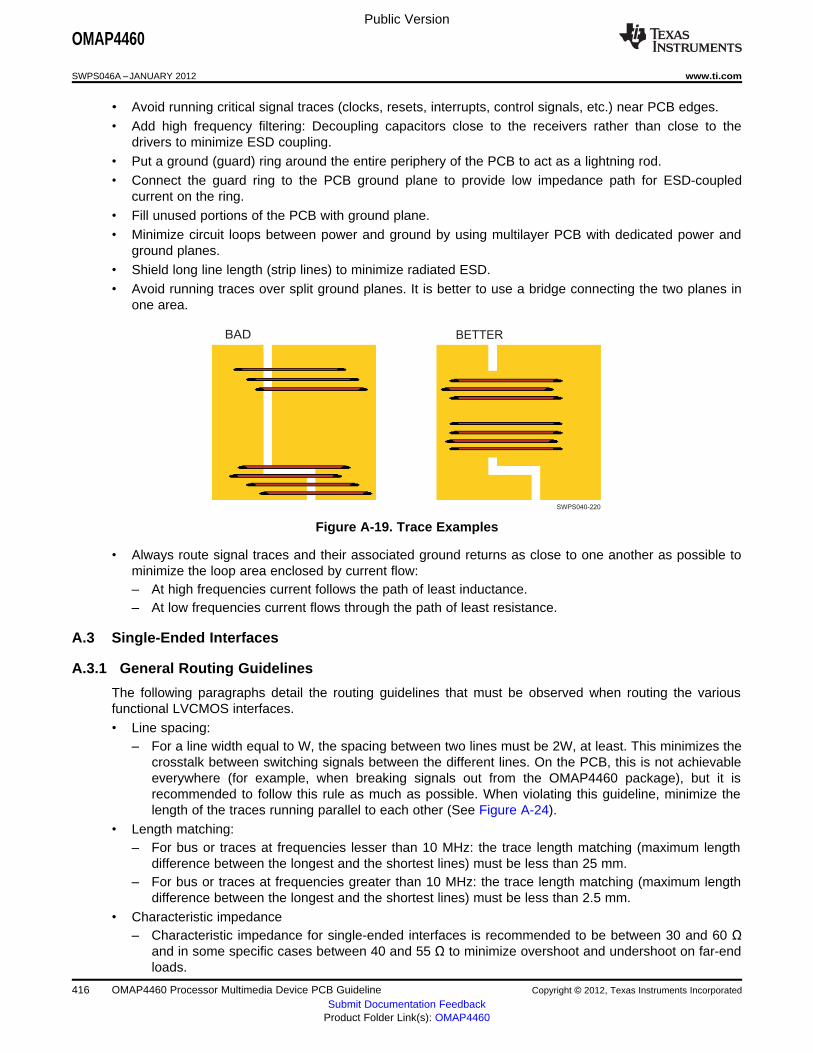
BAD BETTER
SWPS040-220
Public Version
OMAP4460
SWPS046A –JANUARY 2012 www.ti.com
• Avoid running critical signal traces (clocks, resets, interrupts, control signals, etc.) near PCB edges.• Add high frequency filtering: Decoupling capacitors close to the receivers rather than close to the
drivers to minimize ESD coupling.• Put a ground (guard) ring around the entire periphery of the PCB to act as a lightning rod.• Connect the guard ring to the PCB ground plane to provide low impedance path for ESD-coupled
current on the ring.• Fill unused portions of the PCB with ground plane.• Minimize circuit loops between power and ground by using multilayer PCB with dedicated power and
ground planes.• Shield long line length (strip lines) to minimize radiated ESD.• Avoid running traces over split ground planes. It is better to use a bridge connecting the two planes in
one area.
Figure A-19. Trace Examples
• Always route signal traces and their associated ground returns as close to one another as possible tominimize the loop area enclosed by current flow:– At high frequencies current follows the path of least inductance.– At low frequencies current flows through the path of least resistance.
A.3 Single-Ended Interfaces
A.3.1 General Routing Guidelines
The following paragraphs detail the routing guidelines that must be observed when routing the variousfunctional LVCMOS interfaces.• Line spacing:
– For a line width equal to W, the spacing between two lines must be 2W, at least. This minimizes thecrosstalk between switching signals between the different lines. On the PCB, this is not achievableeverywhere (for example, when breaking signals out from the OMAP4460 package), but it isrecommended to follow this rule as much as possible. When violating this guideline, minimize thelength of the traces running parallel to each other (See Figure A-24).
• Length matching:– For bus or traces at frequencies lesser than 10 MHz: the trace length matching (maximum length
difference between the longest and the shortest lines) must be less than 25 mm.– For bus or traces at frequencies greater than 10 MHz: the trace length matching (maximum length
difference between the longest and the shortest lines) must be less than 2.5 mm.• Characteristic impedance
– Characteristic impedance for single-ended interfaces is recommended to be between 30 and 60 Ωand in some specific cases between 40 and 55 Ω to minimize overshoot and undershoot on far-endloads.
416 OMAP4460 Processor Multimedia Device PCB Guideline Copyright © 2012, Texas Instruments Incorporated
Submit Documentation FeedbackProduct Folder Link(s): OMAP4460
Public Version
OMAP4460
www.ti.com SWPS046A –JANUARY 2012
A.3.2 Single-Ended PCB Guideline in OMAP4
A.3.2.1 OMAP4460 Single-Ended Interfaces—PCB Guideline
The following interfaces follow the general guideline of single-ended interfaces.
A.3.2.1.1 OMAP4460 Single-Ended Interfaces—GPMC PCB Guideline
NOTEGPMC: For more information on PCB guideline, see Section 5.4.1, General-Purpose MemoryController (GPMC), especially the timing condition tables, PCB Conditions part.
A.3.2.1.2 OMAP4460 Single-Ended Interfaces—DISPC PCB Guideline
NOTEDISPC: For more information on PCB guideline, see Section 5.5.2.1.1, DSS—DISPC—QuadeXtended Graphics Array (QXGA) Application—SDR Mode, especially the timing conditiontables, PCB Conditions part.
A.3.2.1.3 OMAP4460 Single-Ended Interfaces—RFBI LCD Panel PCB Guideline
NOTERFBI MIPI DBI 2.0: For more information on PCB guideline, see Section 5.5.2.2.1,DSS—Remote Frame Buffer Interface (RFBI)—MIPI DBI2.0—LCD Panel, especially thetiming condition tables, PCB Conditions part.
A.3.2.1.4 OMAP4460 Single-Ended Interfaces—RFBI DLP Pico PCB Guideline
NOTERFBI MIPI Pico DLP: For more information on PCB guideline, see Section 5.5.2.2.2,DSS—Remote Frame Buffer Interface (RFBI)—Pico DLP, especially the timing conditiontables, PCB Conditions part.
A.3.2.1.5 OMAP4460 Single-Ended Interfaces—McBSP PCB Guideline
NOTEMcBSP: For more information on PCB guideline, see Section 5.6.1, Multichannel BufferedSerial Port (McBSP), especially the timing condition tables, PCB Conditions part.
A.3.2.1.6 OMAP4460 Single-Ended Interfaces—McASP PCB Guideline
NOTEMcASP: For more information on PCB guideline, see Section 5.6.2, Multichannel BufferedSerial Port (McASP), especially the timing condition tables, PCB Conditions part.
A.3.2.1.7 OMAP4460 Single-Ended Interfaces—McSPI PCB Guideline
NOTEMcSPI: For more information on PCB guideline, see Section 5.6.3, Multichannel Serial PortInterface (McSPI), especially the timing condition tables, PCB Conditions part.
Copyright © 2012, Texas Instruments Incorporated OMAP4460 Processor Multimedia Device PCB Guideline 417Submit Documentation Feedback
Product Folder Link(s): OMAP4460

Public Version
OMAP4460
SWPS046A –JANUARY 2012 www.ti.com
A.3.2.1.8 OMAP4460 Single-Ended Interfaces—DMIC PCB Guideline
NOTEDMIC: For more information on PCB guideline, see Section 5.6.4, Digital Microphone(DMIC), especially the timing condition tables, PCB Conditions part.
A.3.2.1.9 OMAP4460 Single-Ended Interfaces—McPDM PCB Guideline
NOTEMcPDM: For more information on PCB guideline, see Section 5.6.5, Multichannel PulseDensity Modulation (McPDM), especially the timing condition tables, PCB Conditions part.
A.3.2.1.10 OMAP4460 Single-Ended Interfaces—SlimBus PCB Guideline
NOTESlimBus: For more information on PCB guideline, see Section 5.6.6, SlimBus, especially thetiming condition tables, PCB Conditions part.
A.3.2.1.11 OMAP4460 Single-Ended Interfaces—HSI PCB Guideline
NOTEHSI: For more information on PCB guideline, see Section 5.6.7, High-Speed SynchronousInterface (HSI), especially the timing condition tables, PCB Conditions part.
A.3.2.1.12 OMAP4460 Single-Ended Interfaces—USB PCB Guideline
NOTEUSB: For more information on PCB guideline, see Section 5.6.8, Universal Serial Bus (USB),especially the timing condition tables, PCB Conditions part.
A.3.2.1.13 OMAP4460 Single-Ended Interfaces—I2C PCB Guideline
NOTEI2C: For more information on PCB guideline, see Section 5.6.9, Inter-Integrated CircuitInterface (I2C), especially the timing condition tables, PCB Conditions part.
A.3.2.1.14 OMAP4460 Single-Ended Interfaces—UART PCB Guideline
NOTEUART: For more information on PCB guideline, see Section 5.6.11, Universal AsynchronousReceiver Transmitter (UART), especially the timing condition tables, PCB Conditions part.
418 OMAP4460 Processor Multimedia Device PCB Guideline Copyright © 2012, Texas Instruments Incorporated
Submit Documentation FeedbackProduct Folder Link(s): OMAP4460

Public Version
OMAP4460
www.ti.com SWPS046A –JANUARY 2012
A.3.2.1.15 OMAP4460 Single-Ended Interfaces—SDMMC PCB Guideline
NOTESDMMC: For more information on PCB guideline, see Section 5.7.1, Multimedia MemoryCard and Secure Digital IO Card (SDMMC), especially the timing condition tables, PCBConditions part.
For more information on SDMMC ESD guideline examples, see Section A.3.2.2.1, ESDImplementation—MMC/SD/SDIO 1 Interface—SD Mode.
A.3.2.1.16 OMAP4460 Single-Ended Interfaces—TPIU PCB Guideline
NOTETPIU: For more information on PCB guideline, see Section 5.8.1.1, Trace Port Interface Unit(TPIU), especially the timing condition tables, PCB Conditions part.
A.3.2.1.17 OMAP4460 Single-Ended Interfaces—STM PCB Guideline
NOTESTM: For more information on PCB guideline, see Section 5.8.1.2, System Trace ModuleInterface (STM), especially the timing condition tables, PCB Conditions part.
A.3.2.1.18 OMAP4460 Single-Ended Interfaces—JTAG PCB Guideline
NOTEJTAG: For more information on PCB guideline, see Section 5.8.2, JTAG Interface (JTAG),especially the timing condition tables, PCB Conditions part.
A.3.2.1.19 OMAP4460 Single-Ended Interfaces—cJTAG PCB Guideline
NOTEcJTAG: For more information on PCB guideline, see Section 5.8.3, cJTAG Interface(cJTAG), especially the timing condition tables, PCB Conditions part.
A.3.2.1.20 OMAP4460 Single-Ended Interfaces—KeyPad PCB Guideline
NOTEHere is the routing of the keypad row and column signals (for all keypad signals):
• The trace impedance must be between 20 Ω and 70 Ω.
• Maximum trace length is equal to 20 cm.
A.3.2.1.21 OMAP4460 Single-Ended Interfaces—DM Timer PCB Guideline
NOTEHere is the routing for all DM timer signals:
• The trace impedance must be between 20 Ω and 70 Ω.
• Maximum trace length is equal to 7 cm.
Copyright © 2012, Texas Instruments Incorporated OMAP4460 Processor Multimedia Device PCB Guideline 419Submit Documentation Feedback
Product Folder Link(s): OMAP4460
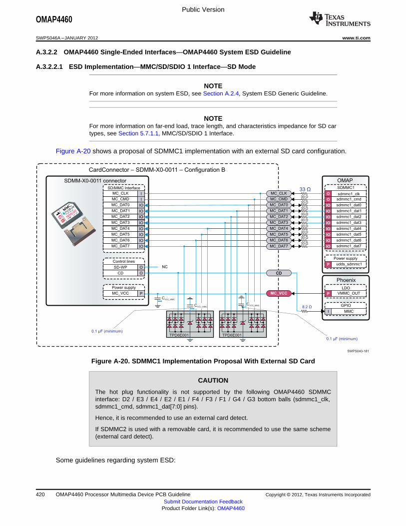
SWPS040-181
sdmmc1_ck
TPD6E001TPD6E001
CardConnector – SDMM-X0-0011 – Configuration B
SDMM-X0-0011 connector
SD/MMC Interface
MC_CLK
MC_CMD
MC_DAT0
I
MC_DAT1
MC_DAT2
MC_DAT3
MC_DAT4
MC_DAT5
MC_DAT6
MC_DAT7
I
IO
IO
IOIO
IO
IO
IO
IO
IO
SD-WP
CD
O
O
PMC_VCC
Power supply
Control lines
NC
0.1 µF (minimum)
0.1 µF (minimum)
33 ΩO
IO
IO
IO
IO
IO
IO
IO
IO
P
P
I
SDMMC1
OMAP
sdmmc1_cmd
sdmmc1_dat0
sdmmc1_dat1
sdmmc1_dat2
sdmmc1_dat3
sdmmc1_dat4
sdmmc1_dat5
sdmmc1_dat6
sdmmc1_dat7
Power supply
udds_sdmmc1
Phoenix
LDO
VMMC_OUT
GPIO
MMC8.2 Ω
MC_VCC
CDCD
MC_DAT7
MC_DAT6
MC_DAT5
MC_DAT4
MC_DAT3
MC_DAT2
MC_DAT1
33 Ω
33 Ω
33 Ω
33 Ω
33 Ω
33 Ω
33 Ω
33 Ω
33 Ω
MC_DAT0
MC_CMD
MC_CLK
memory card
PUSH
O
CVCC_MMC
CVCC_MMCCVCC_MMC
sdmmc1_clk
Public Version
OMAP4460
SWPS046A –JANUARY 2012 www.ti.com
A.3.2.2 OMAP4460 Single-Ended Interfaces—OMAP4460 System ESD Guideline
A.3.2.2.1 ESD Implementation—MMC/SD/SDIO 1 Interface—SD Mode
NOTEFor more information on system ESD, see Section A.2.4, System ESD Generic Guideline.
NOTEFor more information on far-end load, trace length, and characteristics impedance for SD cartypes, see Section 5.7.1.1, MMC/SD/SDIO 1 Interface.
Figure A-20 shows a proposal of SDMMC1 implementation with an external SD card configuration.
Figure A-20. SDMMC1 Implementation Proposal With External SD Card
CAUTION
The hot plug functionality is not supported by the following OMAP4460 SDMMCinterface: D2 / E3 / E4 / E2 / E1 / F4 / F3 / F1 / G4 / G3 bottom balls (sdmmc1_clk,sdmmc1_cmd, sdmmc1_dat[7:0] pins).
Hence, it is recommended to use an external card detect.
If SDMMC2 is used with a removable card, it is recommended to use the same scheme(external card detect).
Some guidelines regarding system ESD:
420 OMAP4460 Processor Multimedia Device PCB Guideline Copyright © 2012, Texas Instruments Incorporated
Submit Documentation FeedbackProduct Folder Link(s): OMAP4460
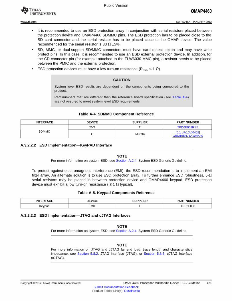
Public Version
OMAP4460
www.ti.com SWPS046A –JANUARY 2012
• It is recommended to use an ESD protection array in conjunction with serial resistors placed betweenthe protection device and OMAP4460 SDMMC pins. The ESD protection has to be placed close to theSD card connector and the serial resistor has to be placed close to the OMAP device. The valuerecommended for the serial resistor is 33 Ω ±5%.
• SD, MMC, or dual-support SD/MMC connectors must have card detect option and may have writeprotect pins. In this case, it is recommended to use an ESD external protection device. In addition, forthe CD connector pin (for example attached to the TLW6030 MMC pin), a resistor needs to be placedbetween the PMIC and the external protection.
• ESD protection devices must have a low turn-on resistance (RDYN ≤ 1 Ω).
CAUTION
System level ESD results are dependent on the components being connected to theproduct.
Part numbers that are different than the reference board specification (see Table A-4)are not assured to meet system level ESD requirements.
Table A-4. SDMMC Component Reference
INTERFACE DEVICE SUPPLIER PART NUMBER
TVS TI TPD6E001RSESDMMC [0.1 uF/10V/0402]C Murata GRM155R71A104KA0
A.3.2.2.2 ESD Implementation—KeyPAD Interface
NOTEFor more information on system ESD, see Section A.2.4, System ESD Generic Guideline.
To protect against electromagnetic interference (EMI), the ESD recommendation is to implement an EMIfilter array. An alternate solution is to use ESD protection array. To further enhance ESD robustness, 5-Ωserial resistors may be placed in between protection device and OMAP4460 keypad. ESD protectiondevice must exhibit a low turn-on resistance ( ≤ 1 Ω typical).
Table A-5. Keypad Components Reference
INTERFACE DEVICE SUPPLIER PART NUMBER
Keypad EMIF TI TPD6F003
A.3.2.2.3 ESD Implementation—JTAG and cJTAG Interfaces
NOTEFor more information on system ESD, see Section A.2.4, System ESD Generic Guideline.
NOTEFor more information on JTAG and cJTAG far end load, trace length and characteristicsimpedance, see Section 5.8.2, JTAG Interface (JTAG), or Section 5.8.3, cJTAG Interface(cJTAG).
Copyright © 2012, Texas Instruments Incorporated OMAP4460 Processor Multimedia Device PCB Guideline 421Submit Documentation Feedback
Product Folder Link(s): OMAP4460
SWPS042-012
TWLpower
V1V8_OUT
OMAP4460
jtag_ntrst
jtag_tck
jtag_rtck
jtag_tmsc
jtag_tdi
jtag_tdo
3.9 W TPD6E001
0.1 F (minimum)m
jtag_ntrst
Vsupply
jtag_tckjtag_rtckjtag_tmscjtag_tdijtag_tdo
Public Version
OMAP4460
SWPS046A –JANUARY 2012 www.ti.com
For a system having JTAG test points accessible to end users (example when located under battery packfor handheld device), system ESD protection can be achieved using TPD6E001 to target 8 kV directcontact. Additional resistors of 3.9 Ω could be used to strengthen ESD robustness.
ESD protection device must exhibit a low turn-on resistance (≤ 1 Ω typical).
Figure A-21. JTAG ESD Protection Example
CAUTION
System level ESD results are dependent on the components being connected to theproduct.
Part numbers that are different than the reference board specification (see Table A-6)are not assured to meet system level ESD requirements.
Table A-6. JTAG Component Reference
INTERFACE DEVICE SUPPLIER PART NUMBER
TVS TI TPD6E001RSEJTAG
C Murata [0.1 uF/10V/0402] GRM155R71A104KA0
A.4 Differential Interface PCB Guidelines
A.4.1 General Routing Guidelines
The following general routing guidelines describe the routing guidelines for MIPI differential lanes.
Each guideline is depicted in detail in Section A.4.2, Three-step Design and Validation Methodology forOMAP Boards.
For more information, you can also refer to the MIPI D-PHY specification v1.00.• As much as possible, no other high frequency signals must be routed in close proximity to the
differential pair.• Must be routed as differential traces on the same layer. The trace width and spacing must be chosen
to yield a 100-Ω differential impedance, along with a 50-Ω single-ended impedance for each signal ofthe pair.
• Due to the fact that the MIPI signals are used for low-power, single-ended signaling in addition to theirhigh-speed differential implementation, the pairs must be loosely coupled.
422 OMAP4460 Processor Multimedia Device PCB Guideline Copyright © 2012, Texas Instruments Incorporated
Submit Documentation FeedbackProduct Folder Link(s): OMAP4460
Public Version
OMAP4460
www.ti.com SWPS046A –JANUARY 2012
• The flight time for the signals must not exceed 2 ns, which assuming a PCB constructed from standardFR-4 material, would imply a maximum trace length of approximately 10” (25.4 cm).
• Minimize external components on differential lanes (like external ESD, probe points).• Through-hole pins are not recommended.• Differential lanes mustn’t cross image planes (ground planes).• No sharp bend on differential lanes.• Number of vias on the differential pairs must be minimized.• Shielded routing is to be promoted as much as possible (for instance, signals must be routed on
internal layers that are inside power and/or ground planes).
A.4.2 Three-step Design and Validation Methodology for OMAP Boards
A.4.2.1 Three-step Design and Validation Methodology—General Guidelines
The following requirements are not dependent on the IO names, such as CSI, DSI, HDMI, and USB,because the differential interfaces basically have the same requirements for the PCB lines.
On the other hand, the PCB requirement is dependent on the operating speed of the circuits because thelength mismatch is given by the bit time (UI) of the signal.
The PCB guidelines for the OMAP differential interfaces are based on the three-step design and validationmethodology in Figure A-22.
The three-step methodology provides a guideline for the design of the PCB differential lines as well as avalidation methodology of the designed differential lines to ensure that the PCB differential lines aredesigned well.
The first step is the general guidelines showing the ideal condition of the PCB differential lines. The firststep is important for the PCB designers because it shows the general requirements for the PCBdifferential lines.
The second step is the length mismatch requirement to satisfy the system-level specification of thedifferential interfaces along with the OMAP package. Step 1 and Step 2 comprise the design guideline.
As a validation methodology, the third step is the frequency-domain specification of the differential linesthat the lines need to satisfy in the frequency domain. If the PCB lines satisfy the frequency-domainspecification, the design is done. Otherwise, the lines need to be improved.
Copyright © 2012, Texas Instruments Incorporated OMAP4460 Processor Multimedia Device PCB Guideline 423Submit Documentation Feedback
Product Folder Link(s): OMAP4460

Step1: General guidelines
1) Draw transmission lines with Z = 50
2) Total conductor length < 100 mm0 W
Step2: Length mismatch for each boardpart of the Transmission line interconnect system(TLIS) assuming no degradation through connectoror cable
1) Intralane length mismatch < UI/300(between N and P lines of a differential pair)
2) Interlane length mismatch < UI/100(between differential pairs)
S-parameter extraction
Step3: Frequency-domain specification guidelines1) A feasible specification is proposed
Design ofboard
Validation ofboard Improvements
SWPS040-183
SWPS040-184
Host board (OMAP)
Host package (OMAP) cable
Device board
Device package
Public Version
OMAP4460
SWPS046A –JANUARY 2012 www.ti.com
Figure A-22. Summary of Three-step PCB Design and Validation Methodology for OMAP4 DifferentialInterfaces
The differential interfaces are connected from the OMAP circuit to the device circuit through the OMAPpackage, OMAP board, cable, device board, and device package.
In this section, the guidelines for the OMAP PCB differential lines are presented.
The PCB guidelines are developed to align the OMAP board with the OMAP package since thespecification of the differential interfaces has one consolidated requirement for the package and board,which can be tested by measurement equipment such as oscilloscopes.
Figure A-23. Transmission Line Interconnect System (TLIS)
The ideal electrical condition of the PCB differential lines is basically the same for all the OMAP differentialinterfaces, which are shown as:• Single-ended Z0 = 50 Ω, differential Z0 = 100 Ω• Negligible length mismatch among differential lines.
The loss of the differential lines is not a big concern because the loss causes intersymbol interference(ISI) that can be compensated by equalization techniques. But, for the differential interfaces withoutequalization techniques, the length is recommended to be kept at a minimum to have a smaller ISI. Forthe OMAP board, we recommend that the length of the PCB differential lines be less than 100 mm.
In the above requirements, the length mismatch requirement is not clear. It is always better to havesmaller length mismatch. But, how small is good enough? To clarify the length mismatch requirement forthe OMAP board lines, we recommend using the below conditions:
424 OMAP4460 Processor Multimedia Device PCB Guideline Copyright © 2012, Texas Instruments Incorporated
Submit Documentation FeedbackProduct Folder Link(s): OMAP4460
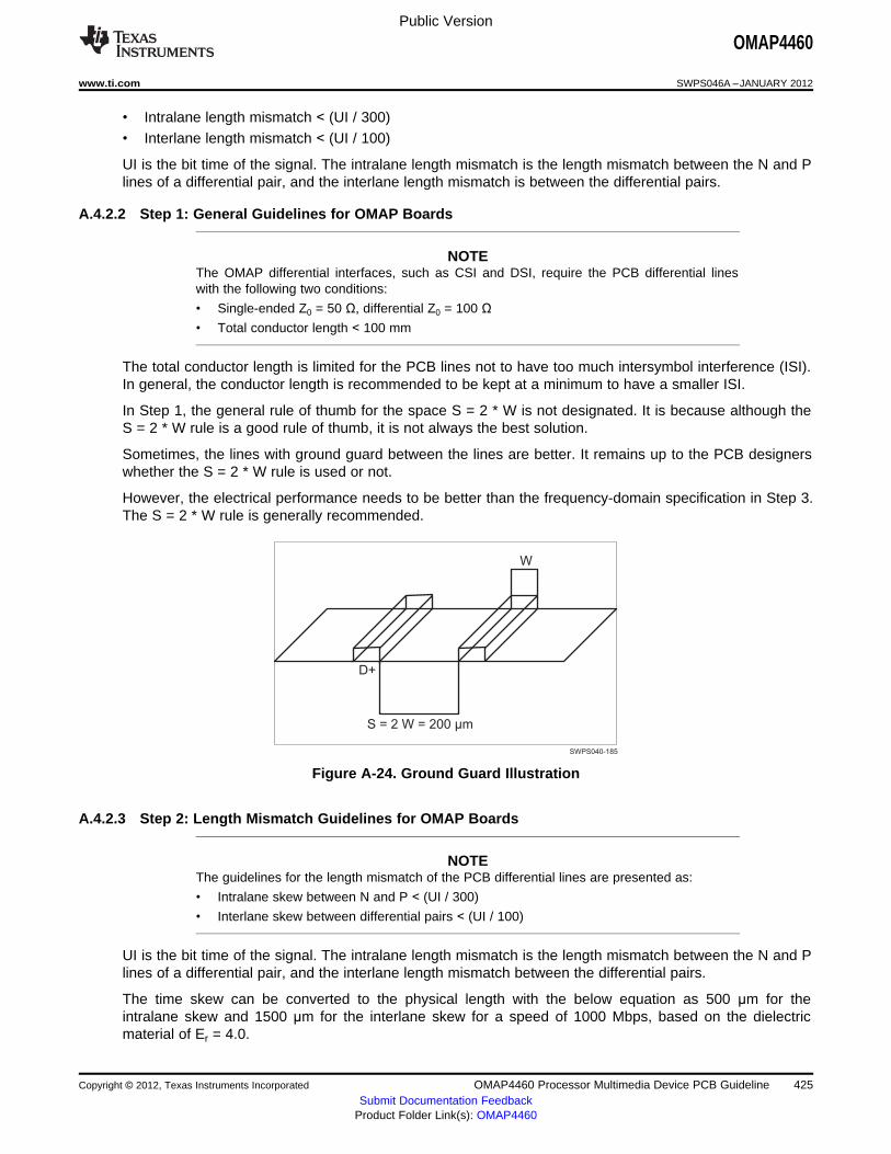
W
D+
S = 2 W = 200 µm
SWPS040-185
Public Version
OMAP4460
www.ti.com SWPS046A –JANUARY 2012
• Intralane length mismatch < (UI / 300)• Interlane length mismatch < (UI / 100)
UI is the bit time of the signal. The intralane length mismatch is the length mismatch between the N and Plines of a differential pair, and the interlane length mismatch is between the differential pairs.
A.4.2.2 Step 1: General Guidelines for OMAP Boards
NOTEThe OMAP differential interfaces, such as CSI and DSI, require the PCB differential lineswith the following two conditions:
• Single-ended Z0 = 50 Ω, differential Z0 = 100 Ω• Total conductor length < 100 mm
The total conductor length is limited for the PCB lines not to have too much intersymbol interference (ISI).In general, the conductor length is recommended to be kept at a minimum to have a smaller ISI.
In Step 1, the general rule of thumb for the space S = 2 * W is not designated. It is because although theS = 2 * W rule is a good rule of thumb, it is not always the best solution.
Sometimes, the lines with ground guard between the lines are better. It remains up to the PCB designerswhether the S = 2 * W rule is used or not.
However, the electrical performance needs to be better than the frequency-domain specification in Step 3.The S = 2 * W rule is generally recommended.
Figure A-24. Ground Guard Illustration
A.4.2.3 Step 2: Length Mismatch Guidelines for OMAP Boards
NOTEThe guidelines for the length mismatch of the PCB differential lines are presented as:
• Intralane skew between N and P < (UI / 300)
• Interlane skew between differential pairs < (UI / 100)
UI is the bit time of the signal. The intralane length mismatch is the length mismatch between the N and Plines of a differential pair, and the interlane length mismatch between the differential pairs.
The time skew can be converted to the physical length with the below equation as 500 µm for theintralane skew and 1500 µm for the interlane skew for a speed of 1000 Mbps, based on the dielectricmaterial of Er = 4.0.
Copyright © 2012, Texas Instruments Incorporated OMAP4460 Processor Multimedia Device PCB Guideline 425Submit Documentation Feedback
Product Folder Link(s): OMAP4460
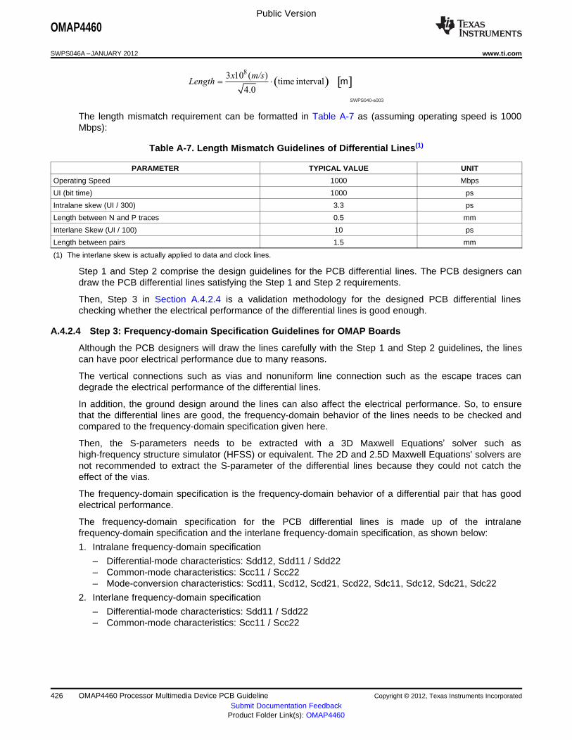
( ) [ ]8
3 10 ( )time interval
4.0
m= ×x m/s
Length
SWPS040-e003
Public Version
OMAP4460
SWPS046A –JANUARY 2012 www.ti.com
The length mismatch requirement can be formatted in Table A-7 as (assuming operating speed is 1000Mbps):
Table A-7. Length Mismatch Guidelines of Differential Lines(1)
PARAMETER TYPICAL VALUE UNIT
Operating Speed 1000 Mbps
UI (bit time) 1000 ps
Intralane skew (UI / 300) 3.3 ps
Length between N and P traces 0.5 mm
Interlane Skew (UI / 100) 10 ps
Length between pairs 1.5 mm
(1) The interlane skew is actually applied to data and clock lines.
Step 1 and Step 2 comprise the design guidelines for the PCB differential lines. The PCB designers candraw the PCB differential lines satisfying the Step 1 and Step 2 requirements.
Then, Step 3 in Section A.4.2.4 is a validation methodology for the designed PCB differential lineschecking whether the electrical performance of the differential lines is good enough.
A.4.2.4 Step 3: Frequency-domain Specification Guidelines for OMAP Boards
Although the PCB designers will draw the lines carefully with the Step 1 and Step 2 guidelines, the linescan have poor electrical performance due to many reasons.
The vertical connections such as vias and nonuniform line connection such as the escape traces candegrade the electrical performance of the differential lines.
In addition, the ground design around the lines can also affect the electrical performance. So, to ensurethat the differential lines are good, the frequency-domain behavior of the lines needs to be checked andcompared to the frequency-domain specification given here.
Then, the S-parameters needs to be extracted with a 3D Maxwell Equations’ solver such ashigh-frequency structure simulator (HFSS) or equivalent. The 2D and 2.5D Maxwell Equations' solvers arenot recommended to extract the S-parameter of the differential lines because they could not catch theeffect of the vias.
The frequency-domain specification is the frequency-domain behavior of a differential pair that has goodelectrical performance.
The frequency-domain specification for the PCB differential lines is made up of the intralanefrequency-domain specification and the interlane frequency-domain specification, as shown below:
1. Intralane frequency-domain specification
– Differential-mode characteristics: Sdd12, Sdd11 / Sdd22– Common-mode characteristics: Scc11 / Scc22– Mode-conversion characteristics: Scd11, Scd12, Scd21, Scd22, Sdc11, Sdc12, Sdc21, Sdc22
2. Interlane frequency-domain specification
– Differential-mode characteristics: Sdd11 / Sdd22– Common-mode characteristics: Scc11 / Scc22
426 OMAP4460 Processor Multimedia Device PCB Guideline Copyright © 2012, Texas Instruments Incorporated
Submit Documentation FeedbackProduct Folder Link(s): OMAP4460

Differential pair 1
p2
p3 p4
p1
SWPS040-186
0
–0.5
–1
–1.5
–2
–2.5
–3
–3.5
–4
–4.5
–50 0.5 1 1.5 2 2.5 3 3.5 4 4.5 5
dB
Frequency (GHz)
Frequency0.1 GHz1 GHz5 GHz
Sdd12> –0.1 dB> –0.5 dB> –2.5 dB
SWPS040-187
Sdd11/Sdd22
Public Version
OMAP4460
www.ti.com SWPS046A –JANUARY 2012
A.4.2.4.1 Intralane Frequency-domain Specification
The port assignment for the intralane frequency domain specification test is shown in Figure A-25. For theintralane specification test, the four ports are assigned to the N and P lines of a differential pair. TheS-parameters can be extracted from dc to 5 GHz.
Figure A-25. Port Assignment for the Intralane Frequency-domain Specification
A.4.2.4.1.1 Sdd12
Sdd12 represents the differential-mode insertion loss of the differential line. Bigger Sdd12 indicates thatthe transmission line has smaller loss. Since the insertion loss is proportional to the length of the lossytransmission line, Sdd12 will be smaller as the length increases.
So for the OMAP board, we recommend that the total conductor length be smaller than 100 mm for thePCB differential lines, whose electrical behavior is similar to that in Figure A-26. The ideal losslessdifferential line has Sdd12 = 1, which is 0 dB. The Sdd12 is recommended to be larger than the below linefrom dc to 5 GHz. If the designed differential lines have lower Sdd12 than the specification, the lines canbe improved by reducing the length of the differential lines.
Figure A-26. Intralane Sdd12 Frequency-domain Specification
A.4.2.4.1.2 Sdd11 / Sdd22
Sdd11 / Sdd22 represents the differential-mode return loss of the differential line. Smaller Sdd11 / Sdd22indicates that the transmission line has smaller return loss. The ideal differential line with Z0 = 50 Ω (Z0diff= 100 Ω) has Sdd11 / Sdd22 = 0, which is –∞ dB. Sdd11 / Sdd22 is tightly related to the differential-modecharacteristic impedance of the differential line. Sdd11 / Sdd22 is recommended to be smaller than thebelow line.
Copyright © 2012, Texas Instruments Incorporated OMAP4460 Processor Multimedia Device PCB Guideline 427Submit Documentation Feedback
Product Folder Link(s): OMAP4460

0
102
dB
Frequency (GHz)SWPS040-188
103
–10
–20
–30
–40
–50
–60
Frequency0.1 GHz1 GHz5 GHz
Sdd11/Sdd22> –35 dB> –20 dB> –5 dB
Sdd11/Sdd22
0
102
dB
Frequency (GHz)SWPS040-189
103
–10
–20
–30
–40
–50
–60
Frequency0.1 GHz1 GHz5 GHz
Scc 11/Scc22> –40 dB> –25 dB> –10 dB
Intralane Scc11/Scc22
Public Version
OMAP4460
SWPS046A –JANUARY 2012 www.ti.com
Figure A-27. Sdd11/Sd22 Frequency-domain Specification
If the designed differential lines have higher Sdd11 / Sdd22 than the specification, the differential lines canbe improved by adjusting the space distance between the N and P lines of a differential pair. It is becausethe differential-mode characteristic impedance is mostly affected by the space.
A.4.2.4.1.3 Scc11 / Scc22
Scc11 / Scc22 represents the common-mode return loss of the differential transmission line. The smallerof Scc11 / Scc22 indicates the transmission line has smaller return loss. Scc11 / Scc22 is tightly related tothe common-mode characteristic impedance of the differential line. The ideal differential line with Z0 = 50Ω (Z0diff = 100 Ω) has Scc11 / Scc22 = 0, which is –∞ dB. Scc11 / Scc22 is recommended to be smallerthan the line below.
Figure A-28. Intralane Scc11/Scc22 Frequency-domain Specification
If the designed differential lines have higher Scc11 / Scc22 than the specification, the differential lines canbe improved by changing the power and ground nets around the lines. It is because the common-modecharacteristic impedance is mostly affected by the power and ground nets around.
428 OMAP4460 Processor Multimedia Device PCB Guideline Copyright © 2012, Texas Instruments Incorporated
Submit Documentation FeedbackProduct Folder Link(s): OMAP4460

0
–0.5
–1
–1.5
–2
–2.5
–3
–3.5
–4
–4.5
–50 0.5 1 1.5 2 2.5 3 3.5 4 4.5 5
dB
Frequency (GHz)
Frequency
0.1 GHz1 GHz5 GHz
Sdc 11,Sdc 12, Sdc 21, Sdc 22Scd 11, Scd 12, Scd 21, Scd 22
>–35 dB>–35 dB> –20 dB
SWPS040-190
Sdc12, Scd12, Scd11, Sdc11
Differential pair 2
Differential pair 3p3 p4
p1 p2
SWPS040-191
Public Version
OMAP4460
www.ti.com SWPS046A –JANUARY 2012
A.4.2.4.1.4 Scd11, Scd12, Scd21, Scd22, Sdc11, Sdc12, Sdc21, Sdc22
Scd11, Scd12, Scd21, Scd22, Sdc11, Sdc12, Sdc21 and Sdc22 represent the mode-conversion factorsbetween the common-mode signal and the differential-mode signal. The lower number means that theconversion is smaller. They are recommended to be smaller than the below line. If the designeddifferential lines have higher mode-conversion factors than the specification, the differential lines can beimproved by improving the symmetry between the N and P lines of a differential pair. If the two lines areperfectly symmetric, the mode-conversion factors will be 0, which is –∞ dB.
Figure A-29. Intralane Scd11, Scd12, Sdc11, Sdc12 Frequency-domain Specification
A.4.2.4.2 Interlane Frequency-domain Specification
In this section, the interlane frequency-domain specification is described between differential lines. In theinterlane specification test, one line is chosen from a differential pair and the other line is chosen fromanother differential pair, as shown in Figure A-30. Then, the S-parameters will be extracted from dc to 5GHz with a 3D Maxwell Equation solver such as high-frequency structure simulator (HFSS) or equivalent,and the frequency-domain behavior will be compared to the frequency-domain specification given here.Since it is desired that the crosstalk between differential pairs be smaller, the differential-mode andcommon-mode characteristics requirement is stricter than the intralane specification.
Figure A-30. Port Assignment for the Interlane Frequency-domain Specification
Copyright © 2012, Texas Instruments Incorporated OMAP4460 Processor Multimedia Device PCB Guideline 429Submit Documentation Feedback
Product Folder Link(s): OMAP4460

0
102
dB
Frequency (GHz)SWPS040-192
103
–10
–20
–30
–40
–50
–60
Frequency0.1 GHz1 GHz5 GHz
Sdd 11/Sdd 22> –40 dB> –25 dB> –10 dB
Interlane Sdd11/Sdd22
Public Version
OMAP4460
SWPS046A –JANUARY 2012 www.ti.com
A.4.2.4.2.1 Sdd11 / Sdd22
Sdd11 / Sdd22 represents the differential-mode return loss of the two lines. The ideal condition for theinterlane specification is to place the two lines far away from each other not to have any crosstalk. Then,the ideal interlane Sdd11 / Sdd22 = 0, which is –∞ dB. Sdd11 / Sdd22 is recommended to be smaller thanthe below line.
Figure A-31. Interlane Sdd11 / Sdd22 Frequency-domain Specification
If the designed differential lines have higher Sdd11 / Sdd22 than the specification, the differential lines canbe improved by two ways. One way is to adjust the space distance between the N and P lines of adifferential pair, and the other way is to put ground/power nets between the two lines to reduce thecrosstalk.
A.4.2.4.2.2 Scc11 / Scc22
Scc11 / Scc22 represents the common-mode return loss of the two lines. The ideal interlane Scc11 /Scc22 =0, which is –∞ dB. Scc11 / Scc22 is recommended to be smaller than the below line. If thedesigned differential lines have higher Scc11 / Scc22 than the specification, the differential lines can beimproved by putting ground/power nets between the two lines.
430 OMAP4460 Processor Multimedia Device PCB Guideline Copyright © 2012, Texas Instruments Incorporated
Submit Documentation FeedbackProduct Folder Link(s): OMAP4460

0
102
dB
Frequency (GHz)SWPS040-193
103
–10
–20
–30
–40
–50
–60
Frequency0.1 GHz1 GHz5 GHz
Scc11/Scc22> –40 dB> –25 dB> –10 dB
Interlane Scc11/Scc22
Public Version
OMAP4460
www.ti.com SWPS046A –JANUARY 2012
Figure A-32. Interlane Scc11 / Scc22 Frequency-domain Specification
A.4.3 MIPI D-PHY PCB Guidelines in OMAP4
NOTEThe PCB general guidelines mentioned in this section are given for the transmission lineinterconnect present on the OMAP board (between OMAP balls and a connector forexample).
For the PCB guidelines of the total interconnect (between TX balls and RX balls), you canrefer to the MIPI D-PHY specification v1.00.
The MIPI D-PHY signals include the CSI21, CSI22, DSI1, and DSI2 interfaces to or from the OMAP4460.For more information regarding the MIPI-PHY signals and corresponding balls, see Section 2.4, SignalDescriptions.
In next section, the PCB guidelines of the following six differential interfaces are presented.• CSI21 and CSI22 MIPI CSI-2 @ 1.0 Gbps• CSI21 and CSI22 MIPI CSI-2 @ 824 Mbps• CSI21 and CSI22 MIPI CSI-2 @ 800 Mbps• DSI1 and DSI2 MIPI DSI1 @ 900 Mbps• DSI1 and DSI2 MIPI DSI1 @ 824 Mbps
A.4.3.1 CSI21 and CSI22 MIPI CSI-2 @ 1 Gbps (Up to 3 Data Lanes, OPP100), @ 824 Mbps (Up to 4 DataLanes, OPP100), @ 800 Mbps (Up to 4 Data Lanes, OPP50) Device PCB Guidelines
CAUTION
If the skew degradation due to the interconnect (from the output transmitter ball to theinput receiver ball) between the clock and the data lanes is less than ±170 ps (instead of±200 ps in the MIPI D-PHY specification), then 1 Gbps per data lane is achievable with4 data lanes at OPP100 operating point. This must be met for an interconnect lengthless than 10 cm.
Copyright © 2012, Texas Instruments Incorporated OMAP4460 Processor Multimedia Device PCB Guideline 431Submit Documentation Feedback
Product Folder Link(s): OMAP4460
Public Version
OMAP4460
SWPS046A –JANUARY 2012 www.ti.com
NOTEThe CSI21 and CSI22 MIPI CSI-2 application timings are described in Section 5.5.1.1,Camera Serial Interface (CSI2) (especially, the timing conditions are specified in the “TimingConditions” tables of this section).
First, the following PCB guidelines for CSI2 working up to 1.0 Gbps are presented based on the three-stepdesign and validation methodology described in Section A.4.2, Three-step Design and ValidationMethodology for OMAP Boards.
For the design of the PCB differential lines on the OMAP board, the PCB designers need to keep in mindthe requirements of Step 1 and Step 2: the characteristic impedance must be 50 Ω, the total length mustbe smaller than 100 mm, and the length mismatch requirements must be satisfied.
Then, after the PCB design is finished, the S-parameters of the PCB differential lines will be extracted witha 3D Maxwell Equation Solver such as high-frequency structure simulator (HFSS) or equivalent, andcompared to the frequency-domain specification as outlined in Step 3 of design methodology. If the PCBlines satisfy the frequency-domain spec, the design is done. Otherwise, the design needs to be improved.
A.4.3.1.1 Step 1: General Guidelines
The general guidelines for the PCB differential lines of CSI2 are given as:• Single-ended Z0 = 50 Ω• Total conductor length on OMAP board < 100 mm.
In the step, the general rule of thumb for the space S = 2 * W is not designated (see Figure A-24). It isbecause although the S = 2 * W rule is a good rule of thumb, it is not always the best solution. Theelectrical performance will be checked with the frequency-domain specification in Step 3. Even though thedesigners does not follow the S = 2 * W rule, the differential lines are ok if the lines satisfy thefrequency-domain specification in Step 3.
A.4.3.1.2 Step 2: Length Mismatch Guidelines
A.4.3.1.2.1 Step 2: Length Mismatch Guidelines—CSI21 and CSI22 MIPI CSI-2 @ 1.0 Gbps
The guidelines of the length mismatch for CSI-2 are presented in Table A-8. The intralane lengthmismatch must be less than 0.5 mm, and the interlane length mismatch must be less than 1.5 mm.
Table A-8. Length Mismatch Guidelines for CSI-2 @ 1.0 Gbps
PARAMETER TYPICAL VALUE UNIT
Operating speed 1000 Mbps
UI (bit time) 1000 ps
Intralane skew (UI / 300) 3 ps
Length between N and P traces 0.5 mm
Interlane skew (UI / 100) 10 ps
Length between pairs 1.5 mm
A.4.3.1.2.2 Step 2: Length Mismatch Guidelines—CSI21 and CSI22 MIPI CSI-2 @ 824 Mbps
The guidelines of the length mismatch for CSI-2 are presented in Table A-9.
Table A-9. Length Mismatch Guidelines for CSI-2 @ 824 Mbps
PARAMETER TYPICAL VALUE UNIT
Operating speed 824 Mbps
432 OMAP4460 Processor Multimedia Device PCB Guideline Copyright © 2012, Texas Instruments Incorporated
Submit Documentation FeedbackProduct Folder Link(s): OMAP4460

Public Version
OMAP4460
www.ti.com SWPS046A –JANUARY 2012
Table A-9. Length Mismatch Guidelines for CSI-2 @ 824 Mbps (continued)
PARAMETER TYPICAL VALUE UNIT
UI (bit time) 1213 ps
Intralane skew (UI / 300) 4 ps
Length between N and P traces 0.6 mm
Interlane skew (UI / 100) 12 ps
Length between pairs 1.8 mm
A.4.3.1.2.3 Step 2: Length Mismatch Guidelines—CSI21 and CSI22 MIPI CSI-2 @ 800 Mbps
The guidelines of the length mismatch for CSI-2 are presented in Table A-10. The intralane lengthmismatch must be less than 0.6 mm, and the interlane length mismatch must be less than 1.8 mm.
Table A-10. Length Mismatch Guidelines for CSI-2 @ 800 Mbps
PARAMETER TYPICAL VALUE UNIT
Operating speed 800 Mbps
UI (bit time) 1250 ps
Intralane skew (UI / 300) 4 ps
Length between N and P traces 0.6 mm
Interlane skew (UI / 100) 12 ps
Length between pairs 1.8 mm
A.4.3.1.3 Step 3: Frequency-domain Specification Guidelines
With the information in Step 1 and Step 2, the PCB designers can draw the PCB differential linessatisfying the Step 1 and Step 2 requirements.
However, although the PCB designers draw the lines carefully, the lines can have poor electricalperformance due to many reasons.
The vertical connections such as vias and nonuniform line connection can degrade the electricalperformance of the differential lines. And the ground design around the lines can also affect the electricalperformance.
So, to ensure that the differential lines are well designed, the frequency-domain behavior must becompared to the frequency-domain specification in Section A.4.2.4, Step 3: Frequency-domainSpecification Guidelines for OMAP Boards.
1. Intralane frequency-domain specification
– Differential-mode characteristics: Sdd12, Sdd11 / Sdd22– Common-mode characteristics: Scc11/Scc22– Mode-conversion characteristics: Scd11, Scd12, Scd21, Scd22, Sdc11, Sdc12, Sdc21, Sdc22
2. Interlane frequency-domain specification
– Differential-mode characteristics: Sdd11 / Sdd22– Common-mode characteristics: Scc11 / Scc22
A.4.3.2 DSI1 and DSI2 MIPI DSI1 @ 900 Mbps (Up to 3 Data Lanes), @ 824 Mbps (Up to 4 Data Lanes)Device PCB Guideline
NOTEThe DSI1 and DSI2 MIPI DSI1 application timings are described in Section 5.5.2.3, DisplaySerial Interface (DSI) (especially, the timing conditions specified in the “Timing Conditions”tables of this section).
Copyright © 2012, Texas Instruments Incorporated OMAP4460 Processor Multimedia Device PCB Guideline 433Submit Documentation Feedback
Product Folder Link(s): OMAP4460
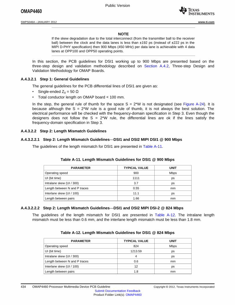
Public Version
OMAP4460
SWPS046A –JANUARY 2012 www.ti.com
NOTEIf the skew degradation due to the total interconnect (from the transmitter ball to the receiverball) between the clock and the data lanes is less than ±192 ps (instead of ±222 ps in theMIPI D-PHY specification) then 900 Mbps (450 MHz) per data lane is achievable with 4 datalanes at OPP100 and OPP50 operating points.
In this section, the PCB guidelines for DSI1 working up to 900 Mbps are presented based on thethree-step design and validation methodology described on Section A.4.2, Three-step Design andValidation Methodology for OMAP Boards.
A.4.3.2.1 Step 1: General Guidelines
The general guidelines for the PCB differential lines of DSI1 are given as:• Single-ended Z0 = 50 Ω• Total conductor length on OMAP board < 100 mm.
In the step, the general rule of thumb for the space S = 2*W is not designated (see Figure A-24). It isbecause although the S = 2*W rule is a good rule of thumb, it is not always the best solution. Theelectrical performance will be checked with the frequency-domain specification in Step 3. Even though thedesigners does not follow the S = 2*W rule, the differential lines are ok if the lines satisfy thefrequency-domain specification in Step 3.
A.4.3.2.2 Step 2: Length Mismatch Guidelines
A.4.3.2.2.1 Step 2: Length Mismatch Guidelines—DSI1 and DSI2 MIPI DSI1 @ 900 Mbps
The guidelines of the length mismatch for DSI1 are presented in Table A-11.
Table A-11. Length Mismatch Guidelines for DSI1 @ 900 Mbps
PARAMETER TYPICAL VALUE UNIT
Operating speed 900 Mbps
UI (bit time) 1111 ps
Intralane skew (UI / 300) 3.7 ps
Length between N and P traces 0.55 mm
Interlane skew (UI / 100) 11.1 ps
Length between pairs 1.66 mm
A.4.3.2.2.2 Step 2: Length Mismatch Guidelines—DSI1 and DSI2 MIPI DSI-2 @ 824 Mbps
The guidelines of the length mismatch for DSI1 are presented in Table A-12. The intralane lengthmismatch must be less than 0.6 mm, and the interlane length mismatch must be less than 1.8 mm.
Table A-12. Length Mismatch Guidelines for DSI1 @ 824 Mbps
PARAMETER TYPICAL VALUE UNIT
Operating speed 824 Mbps
UI (bit time) 1213.59 ps
Intralane skew (UI / 300) 4 ps
Length between N and P traces 0.6 mm
Interlane skew (UI / 100) 12 ps
Length between pairs 1.8 mm
434 OMAP4460 Processor Multimedia Device PCB Guideline Copyright © 2012, Texas Instruments Incorporated
Submit Documentation FeedbackProduct Folder Link(s): OMAP4460

Public Version
OMAP4460
www.ti.com SWPS046A –JANUARY 2012
A.4.3.2.3 Step 3: Frequency-domain Specification Guidelines
The frequency-domain specification is given in Section A.4.2.4, Step 3: Frequency-domain SpecificationGuidelines for OMAP Boards.
A.4.4 USBA0 PHY Interface in OMAP4
The USBA0 interface DP and DM signals are the positive and negative signals from the USB transceivercontained within the OMAP4460. These signals (DP or D+ (usba0_otg_dp) and DM or D–(usba0_otg_dm)) are connected to the OMAP4460 on balls B5 and B4, respectively.
Section A.4.4.1 describes the USBA0 DP and DM PCB guidelines recommended for the OMAP4460device.
A.4.4.1 USBA0 PHY PCB Guideline
The length of DP / DM traces measured between OMAP4 and the common mode choke must follow therequirements detailed in Table A-13 to ensure that the reflections always hit the eye diagram at anoptimum point in the unit interval.
NOTEDistance between the common mode choke filter (ACM2012H in Figure A-33) and IEC ESDprotection (TPD4S012 in Figure A-33) device must be as short as possible: < 30 ps
Similarly, the distance between IEC ESD protection device (TPD4S012DRY in Figure A-33)and the USB connector (Mini A-B receptacle in Figure A-33) must be as short as possible: <30 ps
USB standard connector must be used (micro-AB or mini-AB)
USB grounds must be shorted to the board ground plane with minimum routing (only VIAmust be used to connect to ground plane to avoid loop creation and so to reduceelectromagnetic interference (EMI) effect.
Table A-13. USB Optimized Trace Length
PARAMETER MIN TYP MAX UNIT
DP and DM differential impedance 90 100 ΩDP and DM individual impedance 45 49 ΩTrace length delay for 1 mm 6.66 ps
Recommended intralane mismatch between DP Distance 1 mmand DM Skew 6.66 ps
HS operating speed 480 Mbps
Unit interval (bit time) 2080 ps
Recommended board delay for optimum eye aperture between OMAP and CMF-ESD(1) 510 530 680 ps
Recommended distance between OMAP and CMF-ESD(2) 76.58 79.58 102.10 mm
(1) The board delay is the delay between DP and DM OMAP4 ball levels (usba0_otg_dp and usba0_otg_dm) and the common mode chokefilter (CMF, ACM2012H).For more information see Figure A-33, USB Implementation Proposal with TWL6030 PMIC.
(2) The board distance between the DP and DM OMAP ball level (usba0_otg_dp and usba0_otg_dm) and the common mode choke filter(CMF, ACM2012H) is calculated based on the trace length delay for 1 mm (6.66 ps).
If the above recommended requirement are not possible on customer board, the following requirementsare also possible between the OMAP and the common mode choke. These values have been computedto minimize the bad effect of the reflection on the eye diagram.
Copyright © 2012, Texas Instruments Incorporated OMAP4460 Processor Multimedia Device PCB Guideline 435Submit Documentation Feedback
Product Folder Link(s): OMAP4460

SWPS040-194
USB–OTG
TWL6030
OMAP
USB1 OTG
usba0_otg_dpIODP
DN
CH_EN
usba0_otg_ceO
BATTERY
Power
VBATO
vdda_usba0otg_3p3vP
vssa_usba0otg_3p3vP
usba0_otg_dmIO
USB
IDI
VBUS_B[3:1]P
VUSB PO
CHRG_DET_N_PROG I
CHRG_SW_B[3:1] PO VBAT
vdda_usba0otg_1p8vP
vssa_usba0otgP
LDO
VCXIO P VCXIO
VUSB_3P3TPD4S012
CHRG_BOOT PO
CHRG_CSIN PI
CHRG_CSOUT PI
CHRG_AUXPWR PI
CHRG_PMID_B[3:1]P
CHRG_VREFP
ACM2012H
CFB_USB120 Ø
100 MHz
0.1 µF
CCON_USB
4.7 µF
CEMI_USB
Min
i A-B
rece
pta
cle
CVBUS_USB
CPMID_USB
CVREF_USB
LSW_USB RSNS_USB
CBOOT_USB
CCSIN_USB
CAUXPWR_USB
Public Version
OMAP4460
SWPS046A –JANUARY 2012 www.ti.com
Table A-14. USB Trace Length With N Multiple
PARAMETER MIN TYP MAX UNIT
Unit interval (480 Mbps) 2080 ps
Recommended board characteristics for optimum N = 0 510 530 680 pseye aperture(1)(2)(3) (Recommended Value)
N = 1 1550 1570 1720 ps
N = 2 2590 2610 2760 ps
N = 3 3630 3650 3800 ps
(1) The board delay is the delay between DP and DM OMAP ball levels (usba0_otg_dp and usba0_otg_dm) and the common mode chokefilter (CMF, ACM2012H). For more information see Figure A-33, USB Implementation Proposal with TWL6030 PMIC.
(2) The possible board delay value is calculated as follows:N * ½ * UI + Optimum Board delay (530 ps), with N = 0, 1, 2, or 3.
(3) The board distance between the DP and DM OMAP ball level (usba0_otg_dp and usba0_otg_dm) and the common mode choke filter(CMF, ACM2012H) is calculated based on the trace length delay for 1 mm (6.66 ps).
NOTERemember that the distance between the common mode choke filter (ACM2012H inFigure A-33) and IEC ESD protection (TPD4S012 in Figure A-33) device must be as short aspossible (< 30 ps).
Similarly, for the distance between IEC ESD protection device (TPD4S012DRY inFigure A-33) and the USB connector (Mini A-B receptacle in Figure A-33) must be as shortas possible (< 30 ps).
A.4.4.2 USBA0 PHY Implementation Example
Figure A-33 proposes an example of USBA0 PHY implementation with a TWL6030 PMIC and aTPD4S012 component.
Figure A-33. USB Implementation Proposal with TWL6030 PMIC
436 OMAP4460 Processor Multimedia Device PCB Guideline Copyright © 2012, Texas Instruments Incorporated
Submit Documentation FeedbackProduct Folder Link(s): OMAP4460
Public Version
OMAP4460
www.ti.com SWPS046A –JANUARY 2012
A.4.4.3 ESD Implementation—USBA0 PHY
NOTEFor more information on system ESD, see Section A.2.4, System ESD Generic Guideline.
• ESD: USB standard connector has 4 pins: DP and DM attached to OMAP4460 and ID and VBUS pinsattached to the TLW6030 PMIC IC device.– For DP and DM pins:
• ESD protection device must be preferably an array with a low capacitance (≤ 1.0 pF typical) anda low turn-on resistance (RDYN ≤ 1.2 Ω) while VBUS pin is designed to tolerate 20 V.
• Common mode choke filter (CMF) must be placed between the ESD protection and theOMAP4460 to minimize electromagnetic interference (EMI).
• If CMF is implemented, no isolation resistor is required and system ESD is greatly strengthened.• DC series resistance of the CMF needs to be 1 Ω maximum. Common mode bandwidth (Scc21)
must not exceed 50 MHz.– For VBUS and ID pins:
• For the VBUS pin, a broadband decoupling capacitor reduces noise in the VBUS power line. Inaddition, a large decoupling capacitor will absorb the ESD pulse energy.
• For the ID pin, a chip ferrite bead placed between the ESD protection and the PMIC isrecommended.
NOTESystem level ESD results (following IEC 61000-4-2 standard) are dependent on thecomponents being connected to the product.
Part numbers that are different than the reference board specification described inTable A-15 are not assured to meet system level ESD requirements.
Table A-15. USB Component References
INTERFACE DEVICE SUPPLIER PART NUMBER
USBPHY TVS TI TPD4S012DRY
CMF TDK ACM2012H-900-2P
CFB Murata BLM15PD121SN1
C Murata [1 µF /25V/0603] GRM188R71E105KA12D
EMICAP Murata [0.1 µF /16V ] NFM18PC104R1C3
A.4.5 HDMI Interface in OMAP4
NOTEFor more information on HDMI, please contact your TI representative.
NOTEFor more information on system ESD, see Section A.2.4, System ESD Generic Guideline.
A.5 Clock Guidelines
NOTEFor more information on system clocks, see Section 4, Clock Specifications.
Copyright © 2012, Texas Instruments Incorporated OMAP4460 Processor Multimedia Device PCB Guideline 437Submit Documentation Feedback
Product Folder Link(s): OMAP4460

Cry
sta
l
Cap
X1Via to GND
IC
Cap
Local ground plane
X2
SWPS040-196
Public Version
OMAP4460
SWPS046A –JANUARY 2012 www.ti.com
A.5.1 32-kHz Oscillator Routing
When designing the printed-circuit board:• Keep the crystal as close as possible to the crystal pins X1 and X2.• Keep the trace lengths short and small to reduce capacitor loading and prevent unwanted noise
pickup.• Place a guard ring around the crystal and tie the ring to ground to help isolate the crystal from
unwanted noise pickup.• Keep all signals out from beneath the crystal and the X1 and X2 pins to prevent noise coupling.• Finally, an additional local ground plane on an adjacent PCB layer can be added under the crystal to
shield it from unwanted pickup from traces on other layers of the board. This plane must be isolatedfrom the regular PCB ground plane and tied to the GND pin of the RTC. The plane mustn't be anylarger than the perimeter of the guard ring. Make sure that this ground plane doesn't contribute tosignificant capacitance (a few pF) between the signal line and ground on the connections that run fromX1 and X2 to the crystal.
Figure A-34. Slow Clock PCB Requirements
A.5.2 Oscillator Ground Connection
Although the impedance of a ground plane is low it is, of course, not zero. Therefore, any noise current inthe ground plane causes a voltage drop in the ground. If the two capacitors of the oscillator are connecteddirectly to the ground plane, the voltage drop in the red portion of the ground in Figure A-35 will beoverlaid to the oscillator signals. If the noise related voltage drop is big enough, the oscillator may bedisturbed.
438 OMAP4460 Processor Multimedia Device PCB Guideline Copyright © 2012, Texas Instruments Incorporated
Submit Documentation FeedbackProduct Folder Link(s): OMAP4460
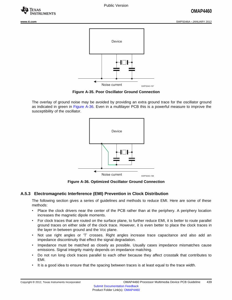
Device
Noise currentSWPS040-197
Device
Noise currentSWPS040-198
Public Version
OMAP4460
www.ti.com SWPS046A –JANUARY 2012
Figure A-35. Poor Oscillator Ground Connection
The overlay of ground noise may be avoided by providing an extra ground trace for the oscillator groundas indicated in green in Figure A-36. Even in a multilayer PCB this is a powerful measure to improve thesusceptibility of the oscillator.
Figure A-36. Optimized Oscillator Ground Connection
A.5.3 Electromagnetic Interference (EMI) Prevention in Clock Distribution
The following section gives a series of guidelines and methods to reduce EMI. Here are some of thesemethods:• Place the clock drivers near the center of the PCB rather than at the periphery. A periphery location
increases the magnetic dipole moments.• For clock traces that are routed on the surface plane, to further reduce EMI, it is better to route parallel
ground traces on either side of the clock trace. However, it is even better to place the clock traces inthe layer in between ground and the Vcc plane.
• Not use right angles or ‘T’ crosses. Right angles increase trace capacitance and also add animpedance discontinuity that effect the signal degradation.
• Impedance must be matched as closely as possible. Usually cases impedance mismatches causeemissions. Signal integrity mainly depends on impedance matching.
• Do not run long clock traces parallel to each other because they affect crosstalk that contributes toEMI.
• It is a good idea to ensure that the spacing between traces is at least equal to the trace width.
Copyright © 2012, Texas Instruments Incorporated OMAP4460 Processor Multimedia Device PCB Guideline 439Submit Documentation Feedback
Product Folder Link(s): OMAP4460
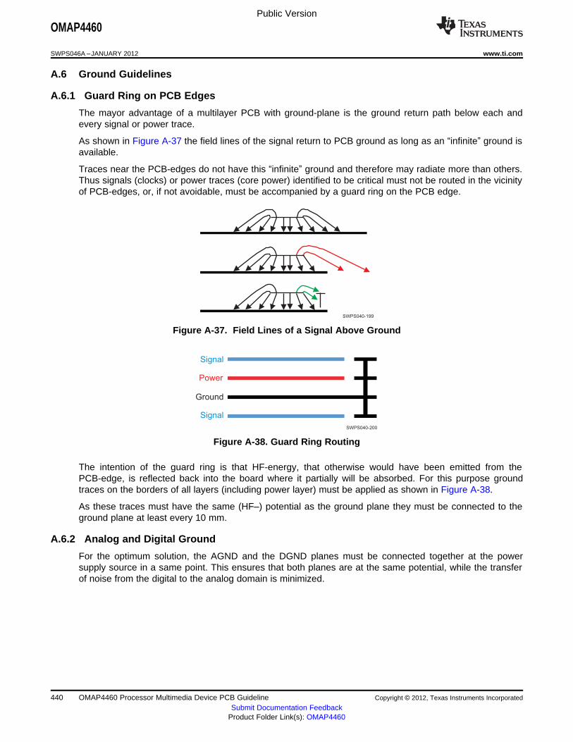
SWPS040-199
Signal
Power
Ground
Signal
SWPS040-200
Public Version
OMAP4460
SWPS046A –JANUARY 2012 www.ti.com
A.6 Ground Guidelines
A.6.1 Guard Ring on PCB Edges
The mayor advantage of a multilayer PCB with ground-plane is the ground return path below each andevery signal or power trace.
As shown in Figure A-37 the field lines of the signal return to PCB ground as long as an “infinite” ground isavailable.
Traces near the PCB-edges do not have this “infinite” ground and therefore may radiate more than others.Thus signals (clocks) or power traces (core power) identified to be critical must not be routed in the vicinityof PCB-edges, or, if not avoidable, must be accompanied by a guard ring on the PCB edge.
Figure A-37. Field Lines of a Signal Above Ground
Figure A-38. Guard Ring Routing
The intention of the guard ring is that HF-energy, that otherwise would have been emitted from thePCB-edge, is reflected back into the board where it partially will be absorbed. For this purpose groundtraces on the borders of all layers (including power layer) must be applied as shown in Figure A-38.
As these traces must have the same (HF–) potential as the ground plane they must be connected to theground plane at least every 10 mm.
A.6.2 Analog and Digital Ground
For the optimum solution, the AGND and the DGND planes must be connected together at the powersupply source in a same point. This ensures that both planes are at the same potential, while the transferof noise from the digital to the analog domain is minimized.
440 OMAP4460 Processor Multimedia Device PCB Guideline Copyright © 2012, Texas Instruments Incorporated
Submit Documentation FeedbackProduct Folder Link(s): OMAP4460
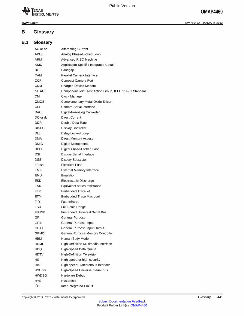
Public Version
OMAP4460
www.ti.com SWPS046A –JANUARY 2012
B Glossary
B.1 GlossaryAC or ac Alternating Current
APLL Analog Phase-Locked Loop
ARM Advanced RISC Machine
ASIC Application-Specific Integrated Circuit
BG Bandgap
CAM Parallel Camera Interface
CCP Compact Camera Port
CDM Charged Device Modem
cJTAG Component Joint Test Action Group, IEEE 1149.1 Standard
CM Clock Manager
CMOS Complementary Metal Oxide Silicon
CSI Camera Serial Interface
DAC Digital-to-Analog Converter
DC or dc Direct Current
DDR Double Data Rate
DISPC Display Controller
DLL Delay-Locked Loop
DMA Direct Memory Access
DMIC Digital Microphone
DPLL Digital Phase-Locked Loop
DSI Display Serial Interface
DSS Display Subsystem
eFuse Electrical Fuse
EMIF External Memory Interface
EMU Emulation
ESD Electrostatic Discharge
ESR Equivalent series resistance
ETK Embedded Trace kit
ETM Embedded Trace Macrocell
FIR Fast Infrared
FSR Full-Scale Range
FSUSB Full-Speed Universal Serial Bus
GP General-Purpose
GPIN General-Purpose Input
GPIO General-Purpose Input Output
GPMC General-Purpose Memory Controller
HBM Human Body Model
HDMI High-Definition Multimedia Interface
HDQ High-Speed Data Queue
HDTV High-Definition Television
HS High speed or high security
HIS High-speed Synchronous Interface
HSUSB High-Speed Universal Serial Bus
HWDBG Hardware Debug
HYS Hysteresis
I2C Inter-Integrated Circuit
Copyright © 2012, Texas Instruments Incorporated Glossary 441Submit Documentation Feedback
Product Folder Link(s): OMAP4460

Public Version
OMAP4460
SWPS046A –JANUARY 2012 www.ti.com
I2S Inter IC Sound
IC Integrated Circuit
ICE In-Circuit Emulator
IEEE Institute of Electrical and Electronics Engineers
IO Input Output
IR Infrared
IrDA Infrared Data Association
ISP Image Sensing Product
ITU International Telecommunications Union
IVA Image and Video Accelerator
JEDEC Joint Electron Device Engineering Council
JPEG Joint Photographic Experts Group (Image format)
JTAG Joint Test Action Group, IEEE 1149.1 standard
LCD Liquid-Crystal Display
LDO Low Dropout
LJF Left-Justified Format
LP Low Power
LVCMOS Low-Voltage CMOS
LVDS Low-Voltage Differential Signaling
McBSP Multichannel Buffered Serial Port
McSPI Multichannel Serial Port Interface
MIPI® Mobile Industry Processor Interface (MIPI® is a registered trademark of Mobile Industry Processor (MIPI)Alliance.)
MIR Medium Infrared
MMC MultiMedia Card
MPU Microprocessor Unit
MS-PRO Memory Stick PRO
NA Not Applicable
NAND Not AND (Boolean Logic)
NOR Not OR (Boolean Logic)
OMAP Open Multimedia Applications Platform
PBGA Plastic Ball Grid Array
PCB Printed Circuit Board
PCM Pulse Code Modulation
PDM Pulse Density Modulation
PD Pull Down
PHY Physical Layer Controller
PLL Phase-Locked Loop
PMIC Power Management Integrated Circuit
POP Package On Package
PU Pull Up
QXGA Quad eXtended Graphics Array
RAW Raw (Image format)
RFBI Remote Frame Buffer Interface
RGB Red Green Blue (Image format)
RMS Root Mean Square
RX Receiver / Receive
SAP TBD
SCL Serial Clock: programmable serial clock used in the I2C interface (can be called also SCLK).
SDA Serial Data: serial data bus in the I2C interface.
442 Glossary Copyright © 2012, Texas Instruments Incorporated
Submit Documentation FeedbackProduct Folder Link(s): OMAP4460
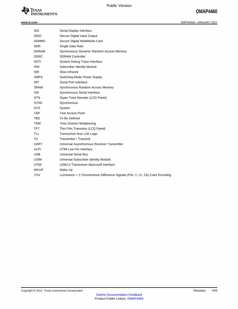
Public Version
OMAP4460
www.ti.com SWPS046A –JANUARY 2012
SDI Serial Display Interface
SDIO Secure Digital Input Output
SDMMC Secure Digital MultiMedia Card
SDR Single Data Rate
SDRAM Synchronous Dynamic Random Access Memory
SDRC SDRAM Controller
SDTI System Debug Trace Interface
SIM Subscriber Identity Module
SIR Slow Infrared
SMPS Switching-Mode Power Supply
SPI Serial Port Interface
SRAM Synchronous Random Access Memory
SSI Synchronous Serial Interface
STN Super Twist Nematic (LCD Panel)
SYNC Synchronous
SYS System
TAP Test Access Point
TBD To Be Defined
TDM Time Division Multiplexing
TFT Thin Film Transistor (LCD Panel)
TLL Transceiver-less Link Logic
TX Transmitter / Transmit
UART Universal Asynchronous Receiver Transmitter
ULPI UTMI Low Pin Interface
USB Universal Serial Bus
USIM Universal Subscriber Identity Module
UTMI USB2.0 Transceiver Macrocell Interface
WKUP Wake-Up
YUV Luminance + 2 Chrominance Difference Signals (PAL Y, Cr, Cb) Color Encoding
Copyright © 2012, Texas Instruments Incorporated Glossary 443Submit Documentation Feedback
Product Folder Link(s): OMAP4460

IMPORTANT NOTICE
Texas Instruments Incorporated and its subsidiaries (TI) reserve the right to make corrections, modifications, enhancements, improvements,and other changes to its products and services at any time and to discontinue any product or service without notice. Customers shouldobtain the latest relevant information before placing orders and should verify that such information is current and complete. All products aresold subject to TI’s terms and conditions of sale supplied at the time of order acknowledgment.
TI warrants performance of its hardware products to the specifications applicable at the time of sale in accordance with TI’s standardwarranty. Testing and other quality control techniques are used to the extent TI deems necessary to support this warranty. Except wheremandated by government requirements, testing of all parameters of each product is not necessarily performed.
TI assumes no liability for applications assistance or customer product design. Customers are responsible for their products andapplications using TI components. To minimize the risks associated with customer products and applications, customers should provideadequate design and operating safeguards.
TI does not warrant or represent that any license, either express or implied, is granted under any TI patent right, copyright, mask work right,or other TI intellectual property right relating to any combination, machine, or process in which TI products or services are used. Informationpublished by TI regarding third-party products or services does not constitute a license from TI to use such products or services or awarranty or endorsement thereof. Use of such information may require a license from a third party under the patents or other intellectualproperty of the third party, or a license from TI under the patents or other intellectual property of TI.
Reproduction of TI information in TI data books or data sheets is permissible only if reproduction is without alteration and is accompaniedby all associated warranties, conditions, limitations, and notices. Reproduction of this information with alteration is an unfair and deceptivebusiness practice. TI is not responsible or liable for such altered documentation. Information of third parties may be subject to additionalrestrictions.
Resale of TI products or services with statements different from or beyond the parameters stated by TI for that product or service voids allexpress and any implied warranties for the associated TI product or service and is an unfair and deceptive business practice. TI is notresponsible or liable for any such statements.
TI products are not authorized for use in safety-critical applications (such as life support) where a failure of the TI product would reasonablybe expected to cause severe personal injury or death, unless officers of the parties have executed an agreement specifically governingsuch use. Buyers represent that they have all necessary expertise in the safety and regulatory ramifications of their applications, andacknowledge and agree that they are solely responsible for all legal, regulatory and safety-related requirements concerning their productsand any use of TI products in such safety-critical applications, notwithstanding any applications-related information or support that may beprovided by TI. Further, Buyers must fully indemnify TI and its representatives against any damages arising out of the use of TI products insuch safety-critical applications.
TI products are neither designed nor intended for use in military/aerospace applications or environments unless the TI products arespecifically designated by TI as military-grade or "enhanced plastic." Only products designated by TI as military-grade meet militaryspecifications. Buyers acknowledge and agree that any such use of TI products which TI has not designated as military-grade is solely atthe Buyer's risk, and that they are solely responsible for compliance with all legal and regulatory requirements in connection with such use.
TI products are neither designed nor intended for use in automotive applications or environments unless the specific TI products aredesignated by TI as compliant with ISO/TS 16949 requirements. Buyers acknowledge and agree that, if they use any non-designatedproducts in automotive applications, TI will not be responsible for any failure to meet such requirements.
Following are URLs where you can obtain information on other Texas Instruments products and application solutions:
Products Applications
Audio www.ti.com/audio Automotive and Transportation www.ti.com/automotive
Amplifiers amplifier.ti.com Communications and Telecom www.ti.com/communications
Data Converters dataconverter.ti.com Computers and Peripherals www.ti.com/computers
DLP® Products www.dlp.com Consumer Electronics www.ti.com/consumer-apps
DSP dsp.ti.com Energy and Lighting www.ti.com/energy
Clocks and Timers www.ti.com/clocks Industrial www.ti.com/industrial
Interface interface.ti.com Medical www.ti.com/medical
Logic logic.ti.com Security www.ti.com/security
Power Mgmt power.ti.com Space, Avionics and Defense www.ti.com/space-avionics-defense
Microcontrollers microcontroller.ti.com Video and Imaging www.ti.com/video
RFID www.ti-rfid.com
OMAP Mobile Processors www.ti.com/omap
Wireless Connectivity www.ti.com/wirelessconnectivity
TI E2E Community Home Page e2e.ti.com
Mailing Address: Texas Instruments, Post Office Box 655303, Dallas, Texas 75265Copyright © 2012, Texas Instruments Incorporated