oled materials q&a session
TRANSCRIPT
Transcript from NanoMarkets Q&A on
OLED Materials Markets
September 2012
Page | 2
NanoMarkets Q&A Session on OLED Materials Markets
NanoMarkets Associate Editor Valerie Coffey interviewed NanoMarkets Senior Analyst, Dr. Jill Simspon and the firm’s Principal Analyst and co-founder, Lawrence Gasman to discuss findings from the firm's recent report, “OLED Materials Markets.” Participants heard the firm's latest perspectives on the evolution of the OLED materials market and how and where NanoMarkets sees the industry unfolding over the coming years. The following is an edited transcript from the call.
Valerie Coffey: Jill, regarding your new report on the OLED materials market, I’d like to ask you: What were your key findings from your research efforts, and how have things changed since the last report on the subject?
Dr. Jill Simpson: Thanks, Valerie. Key findings: probably the biggest key finding – and this should come as no surprise to anyone – is that active-matrix OLED displays are really on the market now in a big way in mobile display products, specifically from Samsung. Samsung’s Galaxy phones actually outsold iPhones a couple of quarters. This will probably change this month when the new iPhone 5 comes out, but it’s still significant because it means that significant sales are flowing into the materials sector now, and that’s definitively new for this report.
Also, you can note that UDC, which is a key materials supplier, had its first profitable quarter last year – the fourth quarter. They also made money again in the second quarter of 2012. This is just one example, but it indicates a clear direction, I think, in the market.
The second key finding is the appearance – or the near appearance, I guess – of OLED TVs. These haven’t become commercially available as quickly as expected, and no doubt they’re still expensive, but the prospects are promising. This is important from this perspective of materials because of the much bigger display size than in mobile devices. They have, simply, a bigger OLED area to coat with materials.
Of course we’ve seen OLED TVs before. Sony had one a few years back, but the current efforts from LG and Samsung are just a little bit more serious and stepped up with respect to marketing activity, size, etc. Sony is even back into the TV market now, having recently partnered with Panasonic. Those two firms are targeting 2013 for their OLED TV launch. Taiwan’s AUO is also targeting 2013 for an OLED TV, so we’ll see. If all of these goals are met, there will be a big change in the size of the OLED materials market.
Finally, I think we have to recognize that OLED lighting is still struggling to get off the ground. We’ll talk more about that later, I think, but it’s important to note that it has made some progress. You can buy products on a wider scale; kits are more widely available now. It’s not just luxury luminaires anymore, even if we have pushed the market takeoff out a couple of years to 2015 or 2016. Here again, OLED lighting will be important from a materials perspective because of the bigger panel areas; bigger OLEDs will quickly increase the size of the OLED materials market.
Page | 3
The final thing that’s really changed, at least since the last time that NanoMarkets did a report on OLED materials, is that the materials sector has moved beyond an IP-building, R&D-only phase. Obviously those things continue – building up of IP is still important and still goes on, but there’s an equal amount of effort now, being put into things that happen when you start actually having sales – things like scale-up, quality control, logistics, business development and marketing.
VC: Can you give us some estimates on how you’re valuing the OLED materials market this year and how you see it growing in the next few years? Have your estimates changed since your last report?
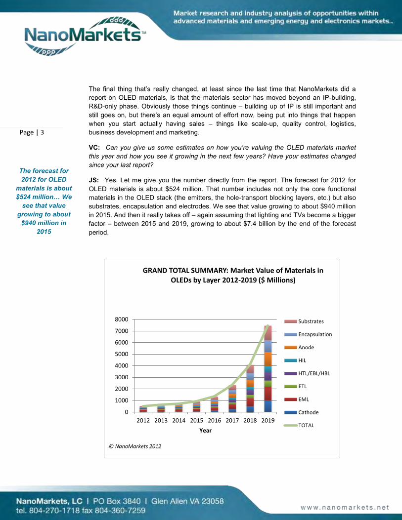
JS: Yes. Let me give you the number directly from the report. The forecast for 2012 for OLED materials is about $524 million. That number includes not only the core functional materials in the OLED stack (the emitters, the hole-transport blocking layers, etc.) but also substrates, encapsulation and electrodes. We see that value growing to about $940 million in 2015. And then it really takes off – again assuming that lighting and TVs become a bigger factor – between 2015 and 2019, growing to about $7.4 billion by the end of the forecast period.
0
1000
2000
3000
4000
5000
6000
7000
8000
2012 2013 2014 2015 2016 2017 2018 2019
Year
GRAND TOTAL SUMMARY: Market Value of Materials in OLEDs by Layer 2012-2019 ($ Millions)
Substrates
Encapsulation
Anode
HIL
HTL/EBL/HBL
ETL
EML
Cathode
TOTAL
© NanoMarkets 2012
The forecast for 2012 for OLED
materials is about $524 million… We
see that value growing to about
$940 million in 2015
Page | 4
Of that total, the value of the core materials – those emitters, hosts, transport, blocking, injection materials, etc., is valued at about $370 million this year and grows to almost $3 billion by the end of the forecast period.
If you look at market share, the core materials values correspond to 70 percent today and 40 percent of the total OLED materials market by the end of the forecast. The percentage goes down because prices of core OLED materials have got further down to go than the electrodes or substrates, but also because utilization is improved.
VC: How did NanoMarkets determine the average layer costs that would correspond to the market values for each material type?
JS: First, all of the market value forecasts that we put together for this report are based on OLED panel shipment forecasts, which are done for each OLED type, whether it’s phones, tablets, TVs, lighting panels, etc. Each of those OLED panel types is given an average display size or average panel size so that we can convert the shipment numbers to total area. We then apply an estimate for yield, which could be different – it is different in OLED lighting versus displays, for example – to get a total OLED area produced. Then, that total OLED area produced forms the basis of the materials forecast.
On the materials side, we build the forecast from the bottom up. For each material we start with assumptions about utilization rates, film thickness, film density, etc., to calculate a total amount of material required to coat the produced OLED area. We then use price estimates, which are estimates of average commercial prices for each material type obtained by talking to both suppliers of materials as well as end users. You can look at catalogue prices in some cases, although of course those don’t usually correspond very closely with what real commercial prices are.
For this year’s report we spent a lot of time refining all of these estimates from the utilization rates to film thickness and to prices, etc., so we think they’re quite reliable. Then to get the market value, we multiply the price by the total quantity used.
In the report, we also present the data in terms of average layer cost so that the reader can compare the costliness of each layer in the OLED. Those values are determined from sales, too. (As such, they’re not derived from different numbers; they’re just presented as a different way of looking at the same data.)
VC: Where are the major OLED materials technology gaps for both lighting and displays that present opportunities for suppliers to come up with better solutions and grab more market share?
JS: Overall – and this is kind of painting a broad brush – but clearly needed by the OLED industry are materials for the functional stack (the emitters, hosts, transport blocking materials, etc.) that enable both higher efficiency and longer lifetime. These are always the goals, and gaps remain in those areas. For example, you need emitters that provide better efficiency and longer lifetimes at the right color points to achieve proper color gamut in displays or the right CRI and color temperature in lighting panels.
Page | 5
If you look at the needs more specifically, in displays what’s missing are dark blue with high efficiency and a longer lifetime. The need for longer lifetime probably means a transition to all-phosphorescent technology. Current blue materials that are on the market work okay for small, mobile displays. They are being used today in the Galaxy phones on the market. But it’s not clear that today’s emitter set is going to work well for larger displays, and more specifically for larger displays that are expected to have longer lifetimes, like televisions. Clearly, a TV should have a longer lifetime than a cell phone. Just how long that lifetime is expected to be is not exactly clear, but it’s certainly longer than in phones. If you’re going to pay thousands and thousands of dollars for that OLED TV, you’re going to expect it to last quite a while.
On the OLED lighting side, the gap is in light blue emitters with high efficiency and longer lifetimes. Here the efficiency piece is even more important because for OLED lighting to take off – I think Lawrence could talk about this as well – it needs to get into some sort of general illumination market like office lighting. To do that, it’s going to have to meet efficiency and lifetime targets.
I think that the DOE’s targets for lifetime and efficiency are 100 lumens per watt and 50,000-plus hours. Today’s materials aren’t quite there. They’re getting there, but they’re not quite there and they have to be, again, because the whole point of alternative lighting, whether OLED or LED or something else, is that it provides higher efficiency than conventional lighting. So, efficiency is critical and materials suppliers have an opportunity to provide products to close that gap.
VC: Many people in the industry, including NanoMarkets, are expecting OLED lighting to be a major contributor to overall revenue. Lawrence, as an expert on OLED markets, can you speak to whether OLED lighting really can compete with LED-based lighting?
LG: I guess the quick answer is “yes.” In some sense, it doesn’t have to. The thing about the display industry is that it seems to be structured in a way that one technology becomes dominant. CRTs have almost gone away now and they’ve been killed off by LCDs. Perhaps, – just perhaps – OLEDs will eventually kill off LCDs, although that could take a human generation. The pattern seems to be that one technology is dominant with a few others buzzing around trying to compete but not doing all that well. Plasma would be a case history you could bring to bear.
Lighting is different. If you want proof that two completely different technologies can coexist, look at fluorescent and incandescent bulbs, which have existed for a couple of human generations now. They certainly compete with each other. They’re economic substitutes at some level, but they seem to coexist.
With OLED lighting, there’s no historical reason that it has to compete with LEDs in a broad sense to do well in the marketplace. I think even the most optimistic forecasters of OLED lighting – I can tell you what we think: that in eight to ten years OLED will be maybe 3 percent of the general illumination market in terms of units shipped, which is not exactly a
Page | 6
huge success story. It just turns out that the revenues are enough to make the suppliers successful.
The other thing about OLED lighting not having to compete with LEDs is they are fundamentally different kind of lights. OLEDs are lighted panels, by definition, that can be integrated into walls and windows (and who knows what else) and create effects that are completely different in terms of functionality and aesthetics than an LED. So, I’m fairly confident that if the numbers are right, LEDs and OLEDs can coexist.
I think the numbers will get right fairly soon. Jill threw out a few numbers. I think, on the efficiency level, industry says that you need to be at 100 to 110 lumens per watt. We’re getting up there. There’s been a lot of success in that field.
When we started covering OLED lighting, not that many years ago, commercial OLEDs were doing about 15 to 20 lumens per watt. At the Light+Building conference and trade show in Germany that’s become a center of OLED lighting displays, what they were showing this year were 40 to 60 lumens-per-watt panels. One hundred to 110 has been achieved in the lab, so I’m pretty sure that within a few years we’ll be there. The question is cost and manufacturing, which speaks to the materials, and I think we’ll be talking more about that as we go on.
VC: Significant efforts are being made to replace vapor deposited functional OLED materials with solution-based ones: LEPs, HILs, ETLs, etc. Jill, what are the market prospects for solution processable materials in OLEDs?
JS: Actually, I think they’re quite good. This is because clearly, at least to me, the most likely path toward actually achieving those larger areas at lower cost involves a transition to solution processing, for the fabrication of as many of the OLED layers as possible.
If you look, however, at solution processing as a group, you can separate it into both polymers and small molecules, and that’s where it gets a little more interesting and different. Sumitomo is just about the only firm left that still is touting polymers in a big way. The rest of the industry, led by DuPont Displays with its solution materials and its partners, as well as UDC, Merck, BASF, etc., seem to have made a bet on small molecules for solution processing. This isn’t to say that there aren’t problems to be solved still in solution processing in order for it to meet expectations, not the least of which is the fact that the performance in a solution material still needs to be generally improved. In other words, matching the performance available or achievable in vapor-based with solution versions still requires work, and that’s an opportunity for materials suppliers to create a competitive advantage around their particular materials.
Also needed are better methods for large-area patterning. Certainly, aerosol jet is one method that has shown some promise, as is nozzle-jet printing, which was developed jointly by Dai Nippon Screen and DuPont Displays. One might say it’s perhaps the most promising of the methods out there since these firms recently licensed their technology to Samsung.
“Matching the performance available or
achievable in vapor-based with solution versions
still requires work, and that’s
an opportunity for materials
suppliers to create a
competitive advantage around
their particular materials.”

Page | 7
Yields are also still an issue in larger area patterning. Still, even given the problems, solution processing seems like it could be the key to getting costs down, especially for something like OLED lighting, which is probably going to rely on the ability to make larger area panels at lower costs – again, as long as performance isn’t sacrificed.
Also, at least one of the OLED TV makers, LG, has already publicly stated the intention to transition at some point to solution processing. Samsung is also looking at solution processing, having licensed technology from Dai Nippon Screens and DuPont Displays. So, Samsung is looking at solution as an enabler for its future.
If you look at this from a numbers perspective, clearly the market value of OLED materials in 2012 is mostly based on vapor deposition, and for the next several years will continue to be mostly based on vapor. But, by the middle of the decade, by 2015, we are looking at a mix of more like 75 percent vapor to 25 percent solution. That could be a little bit optimistic given the delay in getting the first-generation big OLED TVs out. But, by the end of the forecast we have that ratio at more like 60-40.
If you look at polymers, even though we have a total OLED materials market for the core functional materials of about $3 billion by 2019, we’re pretty pessimistic about the prospects for polymers, which we put at somewhere under $150 million through the whole forecast period. Polymer OLEDs have been in the development phase forever, it seems now – at least a decade – and we’ve become pretty skeptical that they will ever emerge from that phase. It’s a possibility that that approach could be abandoned altogether.
VC: That is so interesting. Now, can solution-based or printed other materials, like electrodes, encapsulation layers, etc., achieve the performance necessary to enable truly low-cost manufacturing?
JS: That’s an interesting question and one I think that doesn’t really have a great answer. Today not many good solution-based options exist for “other” materials, for electrodes, certainly not for cathodes.
Also not many solution-based technologies exist for encapsulation. However, if you think about encapsulation being accomplished using a finished barrier film of some kind, which is somehow glued or laminated to a device, then that’s certainly compatible with solution fabrication of OLEDs and potentially inexpensive, assuming those films themselves are not prohibitively expensive.
Also, we see some indication that there is a way to get at least partly there with solution processing for anodes in OLEDs, specifically for transparent electrodes. I’ll let Lawrence talk about that because he’s the expert, having just recently done a report for NanoMarkets on transparent conductors.
LG: First of all, this whole thing about solution processing and printing – just seven years back or so there was a huge amount of enthusiasm about printed electronics. That enthusiasm does not seem to have been justified. I think part of it is matters of fundamental
Page | 8
chemistry. If you’re trying to process something at very low temperatures, it’s harder to get high performance than if you have the ability to heat things up a bit.
The other problem – and I say this as someone who began his business career in the printing industry – is that printing inks are quite hard to make, even if you’re just talking about graphics inks. Electronic inks are even harder because we don’t understand them as well.
With regard to the transparent conductors: at this point, outside of R&D facilities, I’d say just about 100 percent of the transparent conductors used in OLEDs are ITO and deposited using vapor deposition. ITO ink have existed for a long time, but nobody seems to have actually been able – it’s a good example of what both Jill and I were talking about – to create an ITO ink that somebody would want to use outside of R&D.
What’s interesting is that two of the transparent-conductor materials that seem to have some very good prospects – I talked about this at a teleconference that NanoMarkets held last week – are silver-based inks and carbon-nanotube-based inks. Those are mostly being delivered as a printable technology, so if they can find their way into OLEDs – and they might because there’s a long list of reasons why OLEDs would like to do without ITO – that would be an example of a success. These materials are available now in small quantities. Their penetration in OLEDs is still small, but there’s a real-world example for commercial applications. But, we’ve got a long way to go. At the moment the penetration of solution processing for transparent electrodes in OLEDs is exactly zero, I think. So, this is a possibility and it has some potential and may be an opportunity.
Regarding encapsulation, I think Jill said most of this, but that’s got even further to go because it’s not only is the manufacturing process in question, but exactly what kinds of encapsulation OLEDs are going to need and can afford in the future is very much open to speculation. We have a couple of reports coming out on encapsulation late this month, which may be of interest in that regard.
VC: Can you go into the various encapsulation strategies and what are their strengths and weaknesses?
JS: I can do that. First, there was a question earlier about technology gaps that Lawrence just alluded to. Encapsulation still is one of the technology gaps in OLEDs in general. This is probably especially true if we’re looking at moving toward longer lifetime products, TVs, lighting, etc. As he mentioned, we will be releasing two new reports on encapsulation in the next month for both photovoltaics and for OLEDs, so check back for more information.
That said, OLED encapsulation is clearly the most difficult kind of encapsulation because the requirements are at least one – and probably two – orders of magnitude stricter in an OLED than in most other applications. So, this has been a really important area for development and investment and there are several technologies.
The first and most obvious technology for encapsulation is glass. It’s the standard used now. Glass is great because it has excellent barrier properties. It’s transparent. It works
“OLED encapsulation is clearly the most difficult kind of encapsulation because the
requirements are at least one – and
probably two – orders of
magnitude stricter in an OLED than in
most other applications.”
Page | 9
very well for today’s small OLEDs, and clearly an existing glass industry can supply glass with the right properties. There’s a giant display glass industry.
That said, the disadvantages of glass are that it’s expensive, in theory. It’s heavier than others, and when thinner, cheaper materials are desired, people start to think about alternatives. Of course in the long run, if the idea of flexible, or even if just roll-to-roll manufacturing is ever achieved, rigid glass will not work.
The glass industry’s answer is flexible glass. All of the major glass companies are commercializing some version of flexible glass. At the SID show in Boston earlier this year, at least three or four rolls of flexible glass were on the exhibit hall floor. So, it’s out there, too.
The problem with flexible glass is that it’s still pretty expensive, although the argument from the glass industry in favor of flexible glass is that the cost of glass is tied to its weight, so the very lightweight, flexible glass may not be as expensive as you might think. Getting a handle on the real price of the stuff is not that easy. That said, it has a lot going for it. It has the excellent barrier performance that glass does. It has transparency. Drawbacks are availability and price.
Most of the other barrier technologies out there are based on some kind of dyad of alternating layers of polymer and inorganic layer. The goal, no matter who has been working on this, has been to reduce the number of layers required to get a particular barrier performance. Today a few firms are touting availability of two-layer and even single-layer barrier technologies. UDC says it has a single-layer barrier technology. There’s also the Singapore-based firm, Tera-Barrier Films, that has a dyad-type product which is two layers, I think. 3M also has a product on the market. In fact, 3M has something that looks closest to a real product that you can buy, in roll form.
The advantages of a barrier film based on a dyad are that it should be, in theory, lighter and thinner than a cover glass. The disadvantage – outside of performance today, which still lags compared to glass – is cost. Of course the argument for dyad encapsulation is that cost should be lower in the long run for these kinds of encapsulation strategies than it will be for glass. That’s a possibility.
You can also separate the thin film or dyad-type encapsulation into two categories: one where you have the barrier films that you purchase and glue or laminate to a device, as in the 3M product. But you could also directly apply the encapsulation film to an OLED device.
LG: You were talking about the price of flexible glass. We did a report on flexible glass and we think that it has an excellent chance of being a major force to be reckoned with in the OLED space, but it’s ridiculously expensive now and it’s produced in relatively small quantities, so it’s really one of those Catch 22s that somehow the display industry seems to get around, which is: it’s too expensive to use right now even though we want to use it, and it won’t reduce in price until people start to use it.
Page | 10
I think you’ll see some pioneers out there that recognize that glass has got a lot going for it over plastics, and people are looking at OLED displays as the fabric for the flexible displays. We do have a report on flexible glass out now, in addition to the reports on OLED materials that we’re talking about today. This is a scenario we’ve covered quite a lot so I thought I’d add some gloss to the question.
VC: Jump in any time.
JS: OLEDs are probably a really good fit for a flexible glass because they probably can support the cost, at least a little more easily than maybe some other applications, for a while, anyway – at least in some instances.
Getting back to film-type encapsulation, you have the separate films like the 3M products. The advantage of something like that is that it should be cheaper and easier to use from the perspective of a display maker. Also, if there’s a bad area in the film, or an area with imperfections, you can in theory – if you know where that is – be able to remove that from the film and thereby not destroy underlying OLED devices, which are expensive.
Also, if you approach film encapsulation from a separate film perspective you have a little bit more freedom in processing of those films with respect to temperature, for example. The weakness, however, is performance of the films on the market today. You could go to direct encapsulation where you directly deposit your thin film dyad on the devices. That’s a little bit riskier; you have to have very pristine, pinhole-free films. Those are difficult to achieve, but that’s definitely an approach that many display makers are looking at.
One thing that’s interesting is ALD as a possibility for encapsulation. Several ALD equipment makers are looking at OLEDs as a target market. The idea with ALD, compared to CVD or PVD methods, is that it’s better at getting to those really pristine layers, and it also can be done at lower processing temperatures than PVD or CVD can.
The problem with ALD historically has been device-area capability, but this is being improved, so that’s why manufacturers are thinking about using an ALD process for encapsulation.
LG: As a speaker at the Society of Vacuum Coaters Technology Conference earlier this year, I had the opportunity to walk around their exhibition. I was actually surprised, I confess, about how far ALD had come. I tended to think of it as an R&D technology or a very specialized technology in semiconductors, but a bunch of companies were first of all offering the potential for R2R, ALD, sub-high throughput (ALD). A lot of them were focused on the OLED opportunity.
Again, I think that the percentage of OLEDs that use ALD at the moment is close to zero, but at least the ALD manufacturers see OLED as having some potential. When you’re talking about flexible displays and when you’re talking about how OLEDs have so much vulnerability, it seems like ALD is a very interesting area to explore as an opportunity with revenue potential for the equipment manufacturers but also as an enabling technology for
“ALD is a very interesting area to
explore as an opportunity with revenue potential for the equipment manufacturers but also as an enabling
technology for OLED companies that are ambitious
enough to start pursuing flexible,
curvy or even stretchable –
someday – OLED technologies.”
Page | 11
OLED companies that are ambitious enough to start pursuing flexible, curvy or even stretchable – someday – OLED technologies.
In our encapsulation reports coming out in a few weeks, we’ll look at what ALD really means. It’s obviously a rising star in encapsulation. We talked a little bit about encapsulation in the materials report – a lot more granularity in terms of forecasts and actually newer information will be in the encapsulation reports. I just wanted to jump in with my experience of wandering around that particular show.
JS: One final encapsulation technology is metal. It has been used for many years quite well in some OLEDs. It’s been largely displaced in displays because of a move to top-emitting structures, which then necessitated cover glass. But certainly something like OLED lighting could transition back to a bottom-emitting structure – or maybe it already is using that – and metal could become a factor again.
The advantage of metal is that it also has really good barrier performance. Disadvantages are lack of transparency, perhaps, and with respect to weight it’s probably in between glass and plastic.
VC: Thank you. Jill, can you tease us with a few companies in the report that you see as important players in the market, and if any of them have declined in overall importance since the last report?
JS: Clearly the most important players, the ones to watch in OLEDs, are the manufacturers of OLEDs themselves. On the display side, obviously that means Samsung because it’s making 90-plus percent of the active matrix OLEDs on the market today. Also, LG, Sony, etc., are all important. On the lighting side, the big lighting manufacturers, like Philips, Osram, Lumiotec, Konica, Minolta are the key firms. These manufacturers are actually making OLED lighting panels.
Samsung, though, is still the most influential because it manufactures so many of the devices out there. It has announced plans to sell more than a billion OLED displays within the next five years. It has a big plant coming online – I think it was supposed to be this quarter.
That said, Apple is also a key firm to watch that could have a major influence on the OLED materials market. There have been rumors that Apple will shift to OLEDs at some point for some products and when that happens, it will really change the market. It hasn’t done so yet, presumably because of a lack of a supply of OLEDs, and perhaps because Samsung has been either unwilling or unable to manufacture enough. That could change at any time. There’s additional capacity being added; there are other manufacturers that Apple can look to.
Samsung might also decide that revenue from sales of display panels to Apple would outweigh any negatives associated with supplying its main competitor with components. Perhaps the recent judgment against Samsung will make it a little bit more unwilling to work with them for a little bit longer, though.
Page | 12
In terms of declining importance, you have to look, on the lighting side, at GE, which at one time was really active in developing roll-to-roll OLED lighting processes and applications, but it has really been quite silent. I’m pretty sure that GE’s development project still exists, but at a much lower activity level than in the past.
Also, Sumitomo, as I pointed out before is really the only firm out there still touting polymers in a big way. Like I said, that approach could be altogether abandoned at some point.
VC: Interesting.
LG: The other thing I’d mention is the Japanese companies. One of the things we didn’t talk about and nobody talks about much is that OLED displays have been around for a very long time, but in the form of very low-performance passive-matrix displays, and somebody had to supply the materials for that. A select group of Japanese companies has been largely supplying what are now almost obsolete materials. I’m probably exaggerating a little bit.
If we’re looking for companies in potential decline, they would be it. Jill can give more gloss on who they are, but certainly there’s been a shift. UDC has been around a long time, and it’s a company one always thinks of when one thinks about OLED materials. Shift back five or six years and you’d list a bunch of other companies almost automatically – less automatically now, I think.
VC: There are a few key firms like UDC that dominate the OLED materials business now. How does NanoMarkets see revenues derived from licensing and materials supply changing as the market matures? Will other players break through and erode current revenue streams or will they be subsumed by the dominant players?
JS: At least with respect to emitter technology, I think UDC will continue to dominate. But, keep in mind that although we talk about them a lot, it’s because they’re a public company, their income statements are more easily available, and you can link the information directly to what’s going on in the market. But, they still only hold about 50 percent, or maybe even less, of the value of the emitter market since only red and some green materials of theirs are being used. So, it’s really not the only player; it’s just definitely the most visible player.
Also, it’s important to keep in mind that most of UDC’s sales today rely on a single major customer – Samsung – and that’s never a particularly comfortable position for a materials supplier to be in. That said, UDC still has some things going for it. Use of green phosphorescent UDC material is growing, and it’s likely that UDC has as good a chance as anyone – and perhaps better than most – to start selling phosphorescent blue materials if and when they’re developed.
Keep in mind that the whole industry is moving toward all-phosphorescent technology for efficiency, which is especially important in lighting. And when you talk about phosphorescent technology, it automatically brings UDC and its IP position into play. They already have a really extensive network of licensees around for their phosphorescent
Page | 13
technology, and are particularly dominant in Asia where so must of the activity is going on. Samsung is obviously a key licensee, but UDC has a presence elsewhere, as well.
It also has partnerships on the materials side that keep it involved in everything. The IP situation is a little bit uncertain, I suppose. A couple of patents were partially invalidated in Japan earlier in this year, but really only some very broad claims were invalidated. If you dig more deeply you discover that most of the fundamental iridium core IP for phosphorescent OLEDs is upheld. It’s a similar story in the EU and also in Korea, I believe.
Nevertheless, that does open the door a bit for competition. As the market grows, and it’s clearly growing, UDC can definitely expect more attacks on its IP, naturally. Everybody wants to get into this if possible – not to mention the fact that some countries in some regions may simply just devise workarounds or ignore IP altogether. That’s always a possibility.
VC: We’re running a little long. I have another couple of questions I wanted to ask but we might skip them. You can add anything to this if you want. I was going to direct this one to Lawrence and ask him: Heading into the future, how fast will mainstream display makers transition to OLEDs?
LG: I think it will be very slowly. All the evidence from display transitions in the television business is that it happens very slowly. I remember reading, I think in The Economist, that some particular year was the first year that flat-panel televisions actually outsold non-flat-panel televisions. You’d think from all the fuss that that was a very long time ago. I don’t remember exactly when, but it was probably five or six years ago. It just takes a long time in the television industry.
As Jill said, television is particularly important in the context of materials because televisions use a lot of materials, essentially. And I think that will be a very slow transition.
In the mobile display area, the transition will happen much faster. Part of it’s just the mathematics of it because the longevity of a mobile display is just a few years and while we don’t know, really, what the expectations are for TVs anymore, they’re clearly longer than that. Especially, as Jill said, if you’re buying a $10,000 TV you want it to last more than three years – at least I certainly would.
I think mobile displays will transition much faster, but maybe not super fast for two reasons. One of them really has to do with capacity. If you want to buy large numbers of small mobile OLED displays right now you pretty much have to go to Samsung. It’s the only firm producing them in large numbers. So, if you’re Apple you have to do some kind of deal with Samsung. We already talked about this. It’s not that easy after the recent patent infringement dispute.
That will change, though. New plants will open up. New plants are going to open up for sure in China in the next few years, but there’s a constraint on that, too. The other thing that will constrain the change from LCDs to OLEDs is the fact that LCDs are very good at keeping up.
Page | 14
At the SID show, I saw two mobile phones next to each other – both very high-quality displays. One of them was OLED and one of them was some kind of fancy LCD. I asked the representative there, “You know, does this mean that OLEDs are not going to succeed?” He pointed out what was obvious, really – and the impact sort of grew on me – that to get to that quality in an LCD you had to add all sorts of films and filters and who knows what else. That added cost, so the point about OLEDs wasn’t just quality, it was a price per quality unit. I think LCD will try to keep up for quite a while, and it will be successful to some degree before it basically gets out-maneuvered in terms of price.
I think all these things are going to take a while. Of course, we don’t yet know for certain that OLEDs are going to take over. Like the issue of encapsulation; it’s still a big question mark. If you can’t get the encapsulation for OLEDs right and cost effective and you end up with large displays that don’t last very long, then I think the scenarios that we and most other analysts are exploring for OLEDs begin to look a little ropey and unrealistic.
The assumption we’re making is it will continue to grow. It’s got a long way to grow, because the penetration in the display marketplace and certainly the in the lighting marketplace are small. I know you can go out and buy Galaxy phones anytime you want now, but if you look at them as a proportion of the numbers of cell phones sold, with about 1.4 billion cell phones sold every year, the percentage of those that are OLEDs is – Jill would know – pretty darn small.
VC: Thank you. Jill, do you have anything to add to that?
JS: We talked a bit before about key firms to watch, or influential firms. In the interest of time, I glossed over a couple of them. In the report we talk pretty extensively about some of the others that I didn’t mention like Novaled and Mitsubishi and Idemitsu Kosan and some others that are also really influential in this market.
LG: I think some of those companies that you mentioned, especially in OLED actually have been around for years and they’re now beginning to see the light of day. Good news for them – but, also showing the new direction that OLEDs are taking – it’s a bad pun here somewhere – and the visibility that OLEDs are getting. UDC and Pioneer put out the first commercial OLED display that went into a car radio. I don’t remember how long ago that was, but it was a very long time ago. It was too small to get an impression of the new technology at that point.
JS: Around a decade ago, I would think.
LG: Yes, that’s what I thought.
VC: Thank you both. That’s all we have time for, so I’m going to conclude and pass it back to Robert for closing comments. Thank you for this opportunity.
“ If you can’t get the encapsulation for OLEDs right
and cost effective and you end up
with large displays that don’t last very long, then I think the scenarios that we and most other
analysts are exploring for
OLEDs begin to look a little ropey and unrealistic.”
Page | 15
Related NanoMarkets Reports:
Transparent Conductor Markets 2012
OLED Lighting: Companies, Products and Strategies – 2012
NanoMarkets OLED Lighting Market Forecast – Q2 2012
OLED Lighting Materials Markets 2012
Markets for OLED Encapsulation Materials -2011
Markets for OLED Materials - 2011
Visit us at www.nanomarkets.net for a full listing of the firm’s services and reports.