october 2018 advanced patterning technologies
TRANSCRIPT

D u P o n t E l e c t r o n i c s & I m a g i n g
October 2018
AdvancedPatterningTechnologies
George Lu, China Business DirectorLitho Technologies, DuPont Electronics & Imaging

D u P o n t E l e c t r o n i c s & I m a g i n g
Outline
• FinFET Implant
• Multiple Patterning
• 3D NAND
• EUVL
• DowDuPontTM Merger Update

D u P o n t E l e c t r o n i c s & I m a g i n g
Innovative Solutions for Industry Challenges
LELE orLELELELELE orLELELE
SADP orSAQP
SADP orSAQP
EUVLithography
EUVLithography
FinFETImplantFinFETImplant
KrF/ArF BARC or ULKrF/ArF BARC or UL
KrF/ArF ResistKrF/ArF Resist
Gap filling & planarizationWet etch compatibilitySmall CD <80nm
Gap filling & planarizationWet etch compatibilitySmall CD <80nm
PW, LWR, Sensitivity,DefectivityPW, LWR, Sensitivity,Defectivity
LWR, PW, Defectivity, CostreductionLWR, PW, Defectivity, Costreduction
EUV InterlayerEUV Interlayer
193i Resist193i Resist
NTD BARC/HT-SOCNTD BARC/HT-SOC
TC/CTOTC/CTO
EUV Trimming OCEUV Trimming OC
Our SolutionsChallenges
3D NAND3D NANDStaircase Patterning,channel hole CDUStaircase Patterning,channel hole CDU
Thick DUV ResistThick DUV Resist
PTD/NTD BARCPTD/NTD BARC
193i Resist193i Resist
Lithography

D u P o n t E l e c t r o n i c s & I m a g i n g
Material Solutions
FinFET Implant

D u P o n t E l e c t r o n i c s & I m a g i n g
Improving Gap Fill/Planarization & Wet Etch Resistance
Low Tg polymer New X-linker
Flexible chain to reduce Tg Small Mw for gap fill and
planarization
No by-product less shrinkage Lower CA & better
adhesion on metal sub.
High decomposition temp. slow X-linking Maximize thermal mobility
during curing
SampleFilm
shrinkContactAngle
X-linkingtemp
GF@10nmgap, TiN
Wet etch resistance (peel off time)
NH4OH:H2O2:H2
O = 1:1:2, 50 ˚C, TiN
H3PO4 :H2O2=1:1, 60˚C, TiN
HCl:H2O2=1:160˚C, TiN
B101LB 240A 70º 100C Void 30sec 1.5min -
AR™ 274 52A 65º 170C No void 65sec 6min >10min
New TAG
Tg: 25C
Flexible chain
0%
20%
40%
60%
80%
100%
80 100 120 140 160 180 200 220
Rem
ain
ed
TH
K(%
)
Temperature (℃)
14-B010VA 14-B010LB
+ +
X-linker
Stronginteractionwith TiN

D u P o n t E l e c t r o n i c s & I m a g i n g
AR™ 274 BARC: <10nm Gap Fill & Resistance to SC-1
Excellent gap fill w/o void for <10nm gap on TiN substrate Good wet etch resistance : SC-1, H3PO4 /H2O2, HCl/H2O2
Good planarization Optimal optical property (n/k) compatible with KrF and ArF lithography
Curingtemp.
n/kEtch rate
to UV™ 1610Reflectivity(1200A on Si)
Gap fill PlanarizationCompatibility
with RRCthinner
205C~215C1.72/0.18 @248nm1.77/0.17 @193nm
x 1.7 (H2/N2) <3.0%No void
<10nm gapSmall I-D THK
biasGood w/OK73
Litho performance Gap fill @10nm trenchWet etch resistance
100nmTrench / 240nm Pitch
UV™1660, ASML/850, 0.80NA,0.70/0.35s, Annular, Binary
TiN on oxide /Depth=100nm/Gap CD=10nm
NH4OH:H2O2:H2O= 1:1:2, 50˚C
65sec
H3PO4 :H2O2
= 1:1, 60˚C6min
HCl:H2O2
=1:1, 60˚C>10min
Adhesion on TiN wet etch

D u P o n t E l e c t r o n i c s & I m a g i n g
AR™ 277 BARC: Further Improvement in Gap Fill (<7nm)& Wet Etch Resistance
Curingtemp.
n/kEtch rate
to UV™ 1610Reflectivity(1200A on Si)
Gap fill PlanarizationCompatibility
with RRCthinner
205C~215C1.69/0.00 @248nm1.71/0.40 @193nm
x 1.3 (H2/N2) <3.0%
No voidat <7nm
gap
Small I-D THKbias
Good w/OK73
Etch Rate Litho Performance
100nmTrench/ 210nm Pitch
Nikon 610C, 1.35NA, Annular, 0.835/0.589s
110nm Line/ 700nm Pitch
80nm Trench/ 700nm Pitch
Gap fill
TiN on oxideDepth=100nmGap CD=10nm
No void
Excellent gap fill w/o void for <7nm gap on TiN substrate Excellent wet etch resistance : SC-1. H3PO4 /H2O2, HCl/H2O2
Good planarization Optimal optical property (n/k) compatible ArF lithography
NH4OH:H2O2:H2O= 1:1:2, 50˚C
190sec
H3PO4 :H2O2
= 1:1, 60˚C>10min
HCl:H2O2
=1:1, 60˚C>10min
Adhesion on TiN wet etch

D u P o n t E l e c t r o n i c s & I m a g i n g
Reducing Etch Bias by Developing Fast Etching BARCs
Slow etch rate: Large etch bias Need narrower ADI CD to hit ACI
CD target
Fast etch rate: Small etch bias Able to relax ADI CD
Thick BARC to coverhigh topography
Post-Development Post-BARC Open
High Ohnishi parameter for fast etch rate Fast etch rate reduces etch bias
AR™ 284BARC
D u P o n t E l e c t r o n i c s & I m a g i n g
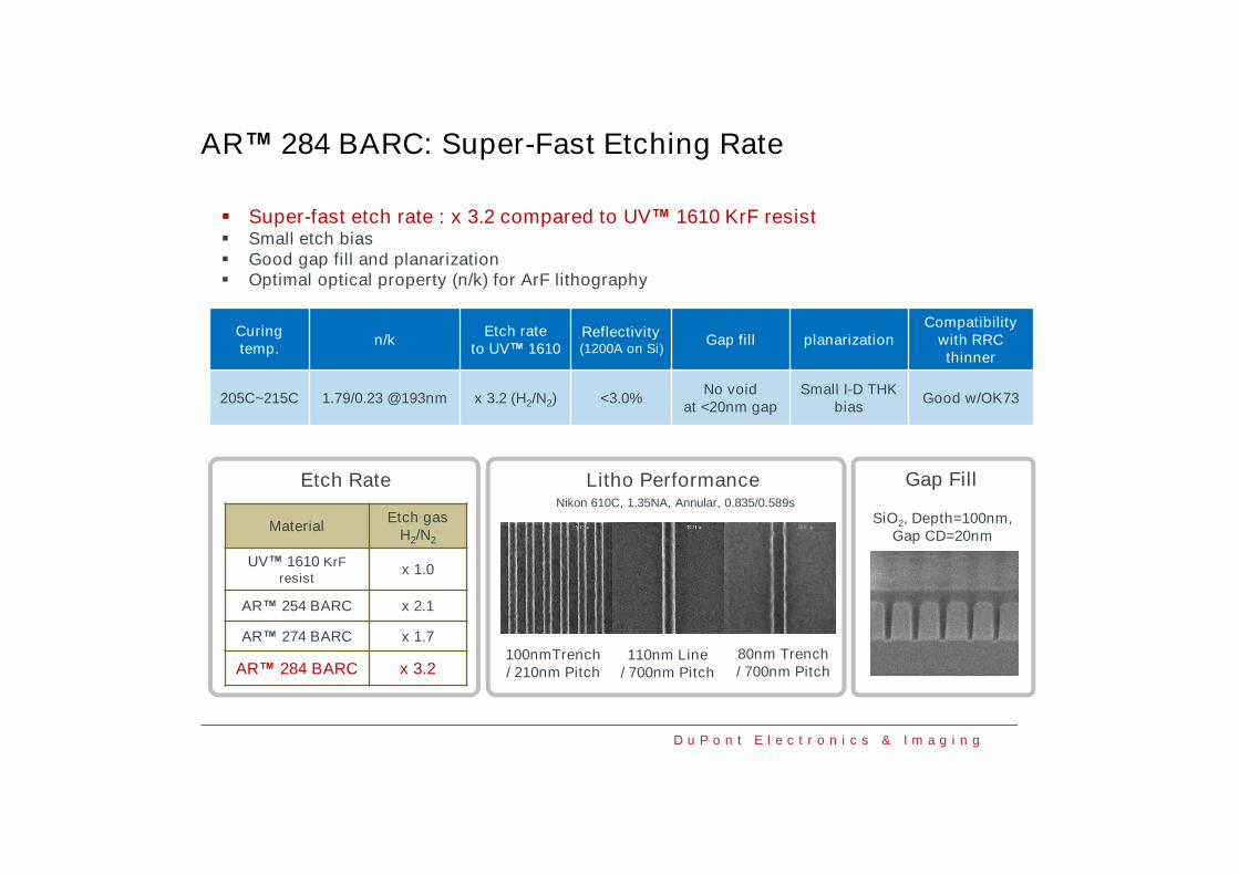
AR™ 284 BARC: Super-Fast Etching Rate
Super-fast etch rate : x 3.2 compared to UV™ 1610 KrF resist Small etch bias Good gap fill and planarization Optimal optical property (n/k) for ArF lithography
Curingtemp.
n/kEtch rate
to UV™ 1610Reflectivity(1200A on Si)
Gap fill planarizationCompatibility
with RRCthinner
205C~215C 1.79/0.23 @193nm x 3.2 (H2/N2) <3.0%No void
at <20nm gapSmall I-D THK
biasGood w/OK73
Litho Performance
MaterialEtch gas
H2/N2
UV™ 1610 KrFresist
x 1.0
AR™ 254 BARC x 2.1
AR™ 274 BARC x 1.7
AR™ 284 BARC x 3.2
Etch Rate
100nmTrench/ 210nm Pitch
Nikon 610C, 1.35NA, Annular, 0.835/0.589s
110nm Line/ 700nm Pitch
80nm Trench/ 700nm Pitch
Gap Fill
SiO2, Depth=100nm,Gap CD=20nm

D u P o n t E l e c t r o n i c s & I m a g i n g
ArF TL (on SiARC)
KrF BL (on BARC)
248nm/193nm Implant Resists for FinFET
• 193nm implant being extensively adopted from 7nm and below• Resolution (small pitch and iso space), LWR and 2D features• Tool availability (248 or 193nm scanner)• Cost (scanner and materials)
Transistor Nanowire?3D Fin FET
D0x/L3Node D1z/L5D1y/L7D1x/L10D20/L14D25/L20D30/L28
2D Planar FET
KrF KrF SL (w/o BARC)
ArF BL (on BARC)ArF SL (w/o BARC)

D u P o n t E l e c t r o n i c s & I m a g i n g
10nm 7nm
DowDuPont’s KrF Implant Resist Portfolio
Wide process window
Low CD Swing Good scum performance on
poly topography
FT=180-400nm
• Good performance on AR™254
• Improved resolution/DOF/profile at 100nm trench
• Improved scum performanceand line distortion on FinFETtopography.
KrF
SL
Rw
/oB
AR
C
16/14nm20nm28nm45nm65nm
Featuresize 180-200nm 140-180nm 100-140nm
UV™ 1610UV™ 1610UV™ 1630
UV™ 1660
UV™ 168G
KrF
Bil
aye
rw
/B
AR
CK
rFS
LR
Ne
ga
tive
General 248nmNegative tone Resist
UVN™ 2300 UVN™ 2310 / 2320 UVN™ 2330 FT=300-1000nm
• FT=200-6000nm
• High resolution and wide PW

D u P o n t E l e c t r o n i c s & I m a g i n g
UV™ 1610
SB/PEB=100C/120C
Mask CD = 120nm
UV™ 1660
SB/PEB=100C/120C
Mask CD = 120nm
UV™ 1610 Resist designed for no BARC UV™ 1660 Resist designed with BARC
UV™ 1660 KrF Resist: Wider DOF & Better Profile on BARC
100nm dense trench (240nmP) on BARC (AR™254) / 0.80NA, 0.70/0.35s Ann.
Process ConditionSubstrate: AR™254 BARC (120nm, 205C/60s)Thickness: 280nmSB: 100ºC,Exposure: NA=0.80, Sigma=0.70/0.35 Ann.PEB: 120ºC,Develop: MF CD-26, 60s, LD-Nozzle

D u P o n t E l e c t r o n i c s & I m a g i n g
Resist Footing over Topography
Positive-tone resist: Footing/residueusually caused by low light intensity atthe bottom and shadowing effect
Negative-tone resist: No footing/residue
Footing /Residue issue
No visible footing
Oxide Oxide
Resist
248nm Negative resist
Resist
Heavy footing
248nm Positive resist

D u P o n t E l e c t r o n i c s & I m a g i n g
+0.55
UVN™ 2320
40.8 mJ/cm2
+0.45 +0.35 +0.25 +0.15 +0.05 -0.05 -0.15 -0.25 -0.35
Focus offset, μm
148.9 176.1 187.0 190.5 200.2 196.5 194.6 148.4 135.2 -----
Opened, CD within 200nm ± 10% (180~220nm) Opened
UVN™ 233035.0 mJ/cm2
183.8 192.2 199.4 202.4 200.9 201.9 198.4 199.2 171.9 134.4
UVN™ 2330 Resist: Wider Process Window
Substrate: 200mm Si
Prime: : HMDS Vapor, 120ºC, 35sec.
SB : 100°C/60sec
Thickness: 318 nm
Exposure: ASML/850, 0.68NA, 0.65PC, Binary MASK, Dark field
PEB : 120°C/60sec
Develop : MF™ CD-26 Developer, 23°C, SP60sec
200nm 1:1 Dense Trench on bare Si
D u P o n t E l e c t r o n i c s & I m a g i n g
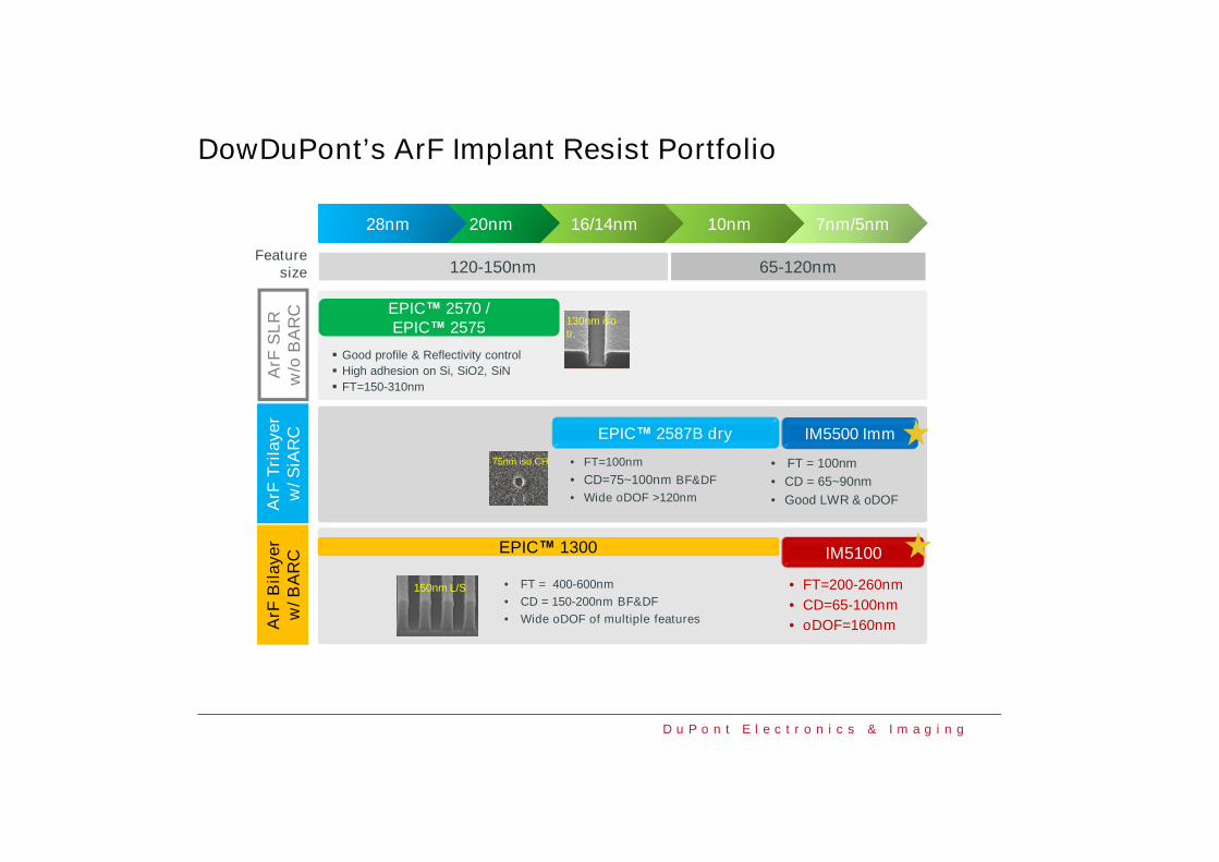
7nm/5nm
DowDuPont’s ArF Implant Resist Portfolio
10nm
Good profile & Reflectivity control
High adhesion on Si, SiO2, SiN
FT=150-310nm
• FT=200-260nm
• CD=65-100nm
• oDOF=160nm
ArF
SL
Rw
/oB
AR
C
16/14nm20nm28nm
Featuresize 120-150nm 65-120nm
EPIC™ 2570 /EPIC™ 2575
IM5100
ArF
Bil
aye
rw
/B
AR
CA
rFT
rila
ye
rw
/S
iAR
C
130nm isotr.
EPIC™ 1300
• FT = 400-600nm
• CD = 150-200nm BF&DF
• Wide oDOF of multiple features
150nm L/S
• FT=100nm
• CD=75~100nm BF&DF
• Wide oDOF >120nm
EPIC™ 2587B dry IM5500 Imm
• FT = 100nm
• CD = 65~90nm
• Good LWR & oDOF
75nm iso CH

D u P o n t E l e c t r o n i c s & I m a g i n g
IM5100 Resist: Good LWR and DoF on BARC
Pattern Top & Down View Parameter IM5100
100nm/210pDense Trench
(Mask CD :100nm/210P)
Eop 32mJ
DoF margin (nm) > 200
E-slope (nm/mJ/cm2) 3.25
LWR (nm) 4.0
90nm/700pIsolated Line(Mask CD :
110nm/700P)
DoF margin (nm) 180
E-slope (nm/mJ/cm2) 3.85
LWR (nm) 3.1
65nm/700pIsolated Trench
(Mask CD :85nm/700P)
DoF margin (nm) 160
E-slope (nm/mJ/cm2) 2.88
LWR (nm) 4.5
BARC Single oBARC on Si wafer
Resist thickness 2600 Å
Exposure NIKON S610C 0.93NA, Annular Sigma: 0.8/0.51 XY pol.
Mask Binary
SB/PEB 110C/60s, 100C/60s

D u P o n t E l e c t r o n i c s & I m a g i n g
IM5500 Resist: Excellent DOF on SiARC
Resist IM5500
Eop18.7mJ / 18.0%
@75nm/180nmP
DOF75nm/180nmP
>180nm
DOF75nm iso Space
>150nm
DOF90nm iso Line
>150nm
DoF90nm Iso Hole
120nm
DoF90nm Iso Post
120nm
oDoFIso Holes/post
115nm
DoF calculated with ProData at 5% EL
StackAR™104 oBARC, 400Å, 175°C/60sXS-110532CA SiARC, 220Å, 240°C/60s
Resist FT 1000Å
Soft-bake 85°C/60s
Exposure ASML/1900i
Illumination 1.35NA , Annular, 0.80o/0.40i
Mask
85nm/180p Space sized to ~75nm1:8 Iso-Space sized to ~75nm1:8 Iso-Line sized to ~90nm
1000p Iso-CH sized to ~90nm1000p Iso-Post sized to ~90nm
PEB 95°C/60s
Development GP-12s
IM5500

D u P o n t E l e c t r o n i c s & I m a g i n g
Summary: Our Implant Solutions for FinFET
248nm Resist• UV™ 1610• UV™ 1630• UVN™ 2330
193nm Resist• EPIC™ 2570
248nm Resist• UV™ 1660• UV™ 217G
193nm Resist• EPIC™ 2587B• IM5500
Underlayer• AR™ 274 (GF>5nm)• AR™ 277 (GF>3nm)• AR™ 284 (FE)• AR™ 201 (GF<5nm)
248nm Resist• UV™ 1660
193nm Resist• IM5100
BARC• AR™ 254 (GF>10nm)• AR™ 274 (GF>5nm)• AR™ 277 (GF>3nm)• AR™ 284 (FE)• AR™ 201 (GF>5nm)• AR™ 210 (UT)• AR™ 602 (DBARC)
Singlelayer
Bilayer Trilayer

D u P o n t E l e c t r o n i c s & I m a g i n g
Material Solutions
Multiple Patterning

D u P o n t E l e c t r o n i c s & I m a g i n g
Continuously Improving LWR for Spacer Multiple Patterning
Low diffusion PAGs Optimization of monomer ratio
New LG withsmall size & low Ea
PDQ(Photo Decomposable Quencher)
Low log P polymer
Higher PAG loadingwith low PEB temp.
LWR2.5 1.5 <1.3
Current status

D u P o n t E l e c t r o n i c s & I m a g i n g
Various Resist Factors Affecting LWR
Exposure
PEB
Development
Polymer aggregationPAG distribution
Deprotection efficiencyLeaving group sizeAcid diffusionQuenching efficiency
Dissolution rateLog P

D u P o n t E l e c t r o n i c s & I m a g i n g
Small Polymer Leaving Group Improves LWR
Small size leaving group:
Smaller free volume afterdeprotection better LWR Exposure
areaFree volume
Bulky sizedLeaving group
Small sizedLeaving group
Before exposure Exposure Development
Small LGBulky LG
45nm/90p L/S, 1.30NA Dipole-35Y(0.97/0.78s)
LWR: 2.6nm(IFU 0.8nm)
LWR: 3.8nm(IFU 1.4nm)

D u P o n t E l e c t r o n i c s & I m a g i n g
PDQ Improves LWR with Better Acid Contrast
Photo Decomposable Quencher enhances acid contrast Improves resolution, LWR an MEEF
LWR=2.81nm
LWR=2.55nm
Conventionalquencher
PDQ
Photo Decomposable Quencher

D u P o n t E l e c t r o n i c s & I m a g i n g
L/S ArF Photoresist Offerings
Node D1z/L5D1y/L7D1x/L10D20/L14D25/L20D30/L28
EPIC™ 1300EPIC™ 1300
IM™5033IM™5033
IM™5035 IM™0208IM™5035 IM™0208
Imm
ers
ion
Dry
EPIC™ 3013/4013EPIC™ 3013/4013
EPIC™ 2099/3099EPIC™ 2099/3099
EPIC™ 2150EPIC™ 2150
w/T
CT
C-f
ree
SADP
Dense LS LWR<1.6nm, FT=80-100nm, CD=40-45nm
Super dense LS (1:0.9 – 1:1) & high resolution at 2D Patterns LWR<2.8nm, FT=80-110nm, CD=37-65nm
37nm/74nmP
43nmL/92nmP (1:1.2)
Good LWR (<3.2nm) Good DOF and PCM
Good LWR
FT=170nm BF &DF Wide DOF (480nm)
90nm/180nmPEPIC™ 2155EPIC™ 2155
FT=200-260nm BF &DF Wide DOF
• FT = 400-600nm, CD = 150-2000nm BF&DF
• Wide oDOF of multiple features
FT=90-120nm, CD=40-45
FT=90-120nm, CD=45-50

D u P o n t E l e c t r o n i c s & I m a g i n g
EPIC™ IM5033 Immersion Resist for SADP
Resist EPIC™ IM5033
Best image
ADI 41nm@ 39/78p, DF
Dense Esize [mJ] 25.1
Dense EL% @ 10% 30.8
Dense EL[nm/mJ] @10%
1.16
BDM [nm] 50.5
PCM [nm] 35.9
Dense FL [nm] @ Es 300
3σ LWR [nm] 2.8
3σ of 20pts CD 0.7
Dow OBARC – dual layered Binary mask ASML 1900i, Dipole 35Y
X-pol, 1.35NA, 0.98/0.86 41nm LS @ 39/78p
LWR 3.3nm(54nm CD)
37nm/74nmP
LWR 3.0nm
Application: Mandrel, Poly & Metal layers
65nm 1to1on 110nm Film
ADI 41nm@ 39/78p, DF
D u P o n t E l e c t r o n i c s & I m a g i n g
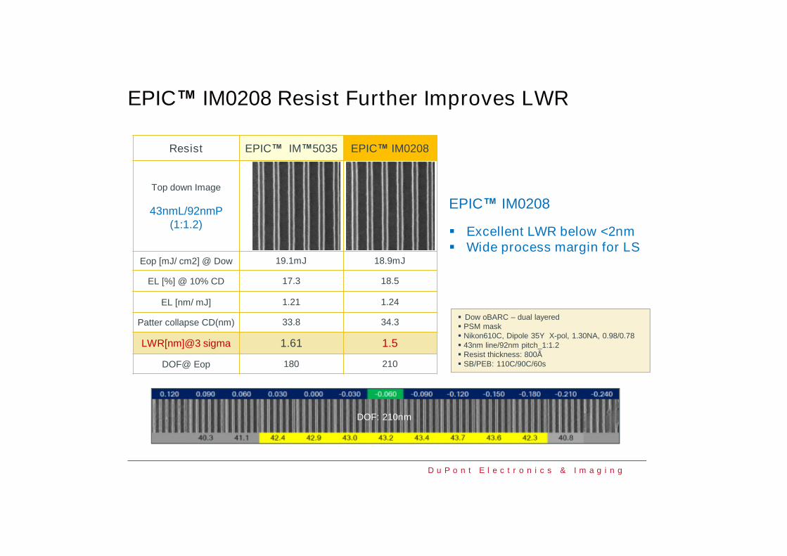
EPIC™ IM0208 Resist Further Improves LWR
Resist EPIC™ IM™5035 EPIC™ IM0208
Top down Image
43nmL/92nmP(1:1.2)
Eop [mJ/ cm2] @ Dow 19.1mJ 18.9mJ
EL [%] @ 10% CD 17.3 18.5
EL [nm/ mJ] 1.21 1.24
Patter collapse CD(nm) 33.8 34.3
LWR[nm]@3 sigma 1.61 1.5
DOF@ Eop 180 210
EPIC™ IM0208
Excellent LWR below <2nm Wide process margin for LS
Dow oBARC – dual layered PSM mask Nikon610C, Dipole 35Y X-pol, 1.30NA, 0.98/0.78 43nm line/92nm pitch_1:1.2 Resist thickness: 800Å SB/PEB: 110C/90C/60s
DOF: 210nm

D u P o n t E l e c t r o n i c s & I m a g i n g
CTO™ Resist Line Trimming Materials
*C. Liu et al., Chemical Trimming Overcoat: An Enhancing Composition and Process for 193nmLithography, Proc. SPIE 2016 paper 9779-67
®
Larger Features
CTO
HeatH+ H+
Develop
Smaller Features

D u P o n t E l e c t r o n i c s & I m a g i n g
Acid Diffusion Controls the Amount of Trimming
Temperature dependenceFickian Diffusion mechanism
DtL 2=
Acid size dependence:

D u P o n t E l e c t r o n i c s & I m a g i n g
47x161
CTO™ Overcoat Offers Excellent Process Window & LWR
Focus (μm)
-0.08
-0.06
-0.04
-0.02
0.00
0.02
0.04
0.06
0.08
70x198 47x167• CTO™ overcoat offers better
process window and patternprofile than over-exposureprocess
• CTO™ overcoat improves LWR
CTO™
LWR
Overdoseno CTO

D u P o n t E l e c t r o n i c s & I m a g i n g
Simplify SADP Process through Spacer over HT-SOC
After Litho SiARC/SOCEtch
HM TemplateEtch
HM TemplateTrimming
Space Depo &Etch
Core Strip SubstrateTransfer Etch
Resist
SiARC
SOC
CVD-HM
Resist
SiARC
SOCskip
SADP over CVD HM
SADP over HT-SOC

D u P o n t E l e c t r o n i c s & I m a g i n g
Improved Performance with New HT-SOC Platform
100nm
250nm
400nm P.SiO2
Si
20nm
84nm P.
TemplateRef.
Gen 1100nm FT
(400oC/60s/Air)
x200k
NewPlatform
100nm FT(170oC/60s/Air +450oC/10m/N2)
∆20nm ∆31nm
~∆1nm ∆23nm
ImprovedPlanarization
New HTSOC
Platform
Excellent PlanarizationAdvantageous Gap FillGood Etch ResistanceSuperior Thermal Properties

D u P o n t E l e c t r o n i c s & I m a g i n g
Material Solutions
3D NAND

D u P o n t E l e c t r o n i c s & I m a g i n g
Thick DUV Resist for 3D NAND
• Every challenging is from high aspect ratio• Most challenging layers:
• Staircase• Channel hole• Staircase contact
Staircase
• Keep 4-6 litho steps for all generations by increasing thickness• Need thick thickness: 12um for 128L• Requires CDU, vertical profile, good thick film properties
Channel hole
• Dense contact at 1500~2000A thickness• PTD or NTD ArF resist• Requires good CD uniformity
Staircasecontact
• Semi-dense and isolated CH at 1300~1600A• PTD or NTD ArF resist• Requires overlap DoF
Metal line• Dense L/S and 2D pattern at 900-1100A• PTD or NTD ArF resist• Requires LWR and overlap DoF for 2D-patterns

D u P o n t E l e c t r o n i c s & I m a g i n g
Requirements for Thick KrF Resist
• No Crack or void• No delamination• Low viscosity• Good coating uniformity
Patterningproperties
• Good CD or slope CD uniformity• Vertical profile: no tailing• Fast photospeed
Thick Filmproperties
Required Performances
Thickness target : 12~15um for 128L and beyond
CDU
Vertical profile
voiddelamination
crack

D u P o n t E l e c t r o n i c s & I m a g i n g
Sample17-K016BB
(=17-K024AA)UV™ 1440
Film thickness 12um 12um
SB/PEB 130C/110C 130C/110C
Esize @3.0μm L/S 98.6mJ 48.0mJ
Top view at bulk pattern corner& Vertical profile
In Wafer CDU, 3σ @3.0μm L/S 49.4nm 38.8nm
CD plot
Viscosity (FT=12μm@1000rpm) --- 300cP
UV™ 1440 Resist: Improved CDU and Profile
Exposure : ASML/850, 0.60NA-0.75s, Conv. , Binary mask
Development : MF™ CD-26, 23°C, 60sec, LD Nozzle
LD Nozzle Scan Direction LD Nozzle Scan Direction

D u P o n t E l e c t r o n i c s & I m a g i n g
Our ArF iBARC Portfolio
32nm
• Thickness : 30 nm• Excellent stack coverage
• Super fast etch rate• Wide process margin
• Low defectivity
AR™ 124 (1.96/0.26)AR™ 124 (1.96/0.26)
High n & low k1st Gen
AR™ 148 (1.96/0.27)AR™ 148 (1.96/0.27)
AR™ 107 (1.85/0.29)AR™ 107 (1.85/0.29)
AR™ 137 (1.96/0.28)AR™ 137 (1.96/0.28)
AR™ 190 (1.96/0.28)AR™ 190 (1.96/0.28)
• High conformality• Good coating over alignment
Device node
• Thin film : 25 nm• Good PR compatibility
28 20 14 10 7
Mid n valuefor thin film
• High k(0.33) value• Wide Process margin on metal layer
AR™ 188 (1.77/0.33)AR™ 188 (1.77/0.33)
High n & low k2nd Gen : High quality& NTD compatibility AR™ 192 (1.96/0.27)AR™ 192 (1.96/0.27)• NTD flexibility

D u P o n t E l e c t r o n i c s & I m a g i n g
High X-linking Density by Polymer Chain Length Control
High film density to reduce intermixing or diffusion with resist or substrate Film Tg & CTE as measurable index
Low CTE by short chain length
AR™192
AR™192

D u P o n t E l e c t r o n i c s & I m a g i n g
Illumination: 1.30NA, Dipole 35X (0.98/0.78s), XY-pol.PR : 15-W003, SB:110C/60sec, PEB:85C/60secBARC : 205C/60sec, Sub. : AR™46, 205C/60sec
EL margin 43/82p@43nm iL/S
DoF margin
Wider Process Margin by High X-linking Density
Eop
DoF : 380 nm
High X-linking degree improves pattern collapse and DoF margin
DoF : 420 nm
DoF : 380 nm
Improved pattern collapse margin
BARC-A
BARC-B
AR™192
BARC-A
BARC-B
AR™192
D u P o n t E l e c t r o n i c s & I m a g i n g
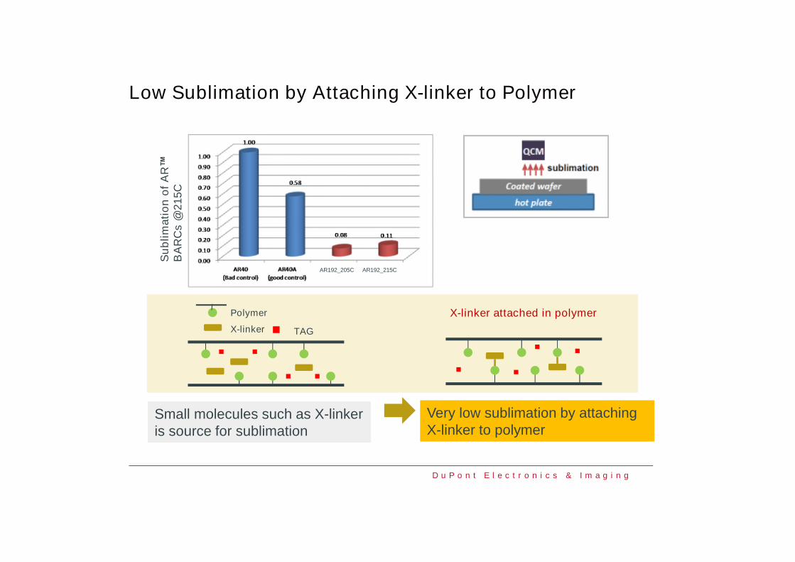
Low Sublimation by Attaching X-linker to Polymer
Very low sublimation by attachingX-linker to polymer
Small molecules such as X-linkeris source for sublimation
X-linker TAG
Polymer X-linker attached in polymer
Su
bli
ma
tio
no
fA
R™
BA
RC
s@
21
5C
AR192_205C AR192_215C

D u P o n t E l e c t r o n i c s & I m a g i n g
Hydrophilic Surface to Match NTD Process
Control of BARC surface energy
• Surface energy matching with exposed resist chemistry Better adhesion
• Hydrophilic surface of BARC Less interaction with hydrophobic developer
RP R
HydrophobicWater CA ~75 °
HydrophilicWater CA 60 – 65°
deprotection
Unexposed Exposed
BARC
PRdeveloperdeveloper
exposure
Hydrophilic surface:Less interaction withnBA
Hydrophilic BARC: better adhesion with exposed resist
ArF Resist Chemistry change after exposure & PEB
• Solvent soluble• High water contact angle
• Solvent insoluble• Low water contact angle
protectedUn-
protected

D u P o n t E l e c t r o n i c s & I m a g i n g
Sample C.A.(˚)
BARC A 68
AR™ 192 BARC 62
Wider EL and DoF with improved collapse margin
Improved NTD Collapse Margin with Low Contact Angle

D u P o n t E l e c t r o n i c s & I m a g i n g
Material Solutions
EUV Lithography

D u P o n t E l e c t r o n i c s & I m a g i n g
EUV Lithography Challenges
Spin on Si-HM
SOC
Sub
CVD HM
SOC
Sub
Better etch selectivity Better post-etch LWR &
CDU
Quad layer
Tri-layer
Insufficient etch selectivityas Si-HM getting htinner
DowDuPont is a leader in EUV IL materials

D u P o n t E l e c t r o n i c s & I m a g i n g
Merger and Split
DowDuPont™

D u P o n t E l e c t r o n i c s & I m a g i n g
Bringing Together Two Complementary Portfolios
With Intention to Create Three Industry-Leading Companies
45
Specialty Products
>300 year combined history of science & innovation creates formidable industry leaders equipped to grow
Materials Science Agriculture

D u P o n t E l e c t r o n i c s & I m a g i n g
Specialty ProductsBroad portfolio of market-leading offerings, proprietary anddifferentiated technologies and a robust pipeline
Electronics &Imaging
Transportation &Advanced Polymers
Safety &Construction
Nutrition &Biosciences
World’s largest supplier with thebroadest set of materials andtechnologies to solve complexproblems for the semiconductor,circuit board, photovoltaic, displayand printing industries.
Product Examples
Kapton®, Cyrel®, Tedlar®,IKONIC™, VISIONPAD™, AR™,EPIC™, SOLDERON™
Industry leader providing high-performance engineering resins,adhesives, lubricants and parts toengineers and designers in thetransportation, electronics andmedical markets.
Product Examples
Zytel®, Hytrel®, Kalrez®,Molykote®, Betaseal®, Vespel®
Global leader in branded productsincluding fibers & foams, aramidpapers, non-wovens, solidsurfaces, membranes andprotective garments serving theworker safety, construction, oil &gas, energy, & transportationmarkets.
Product Examples
Tyvek®, Kevlar®, Nomex®,Corian®, Styrofoam®, Great Stuff®
Industry leader in bio-basedingredients and a biosciencespioneer serving the food, nutrition,pharma, home and personal care,biofuels and animal nutritionmarkets with healthier and moresustainable offerings.
Product Examples
Danisco®, Howaru®, Methocel™,Avicel®, Sorona®, Bio-PDO™,MECS®, BELCO®, STRATCO®,SILVADUR™, KATHON™

D u P o n t E l e c t r o n i c s & I m a g i n g
Semiconductor
Technologies
CMP pads and slurries
Photolithography materials
Advanced packaging materials
Silicon-based CVD & ALD precursors
Silicones for semiconductor packaging
Circuit & IndustrialTechnologies
Metallization materials
Imaging materials
Surface finishes
Photovoltaic and
Advanced Materials
Advanced Printing
Display Technologies OLED materials
Cadmium-free quantum dot materials
Display process chemicals
Silicones for LED packaging
Silicones for display assembly
Removers and cleaners
Polyimide films and laminates
Dry film photoresists
PV metallization pastes
Thick film pastes
Polyvinyl fluoromaterials
Flexographic plates and materials
Digital inks
OLED materials
Display enhancements
PV encapsulants
Sealants for panel assemblyTrichlorosilane for polysilicon wafers
Electronics & Imaging Business Overview

D u P o n t E l e c t r o n i c s & I m a g i n g
Closing Comments• Lithography materials are required for advanced patterning to
enable or improve:
• Scaling
• Pattern fidelity
• Process window
• CD control
• Gap fill/planarization
• Etch resistance
• Defectivity
• DuPont provides a total material solution to address anylithography challenge.

Thank You
©2018 DowDuPont, The Dow Chemical Company, DuPont. All rights reserved.®™ Trademark of DowDuPont, The Dow Chemical Company, E.I. du Pont de Nemours and Company, or their affiliates.

D u P o n t E l e c t r o n i c s & I m a g i n g
SEC Disclosure Rules• Some of our comments include statements about our expectations for the future. Those
expectations involve risks and uncertainties. DowDuPont cannot guarantee the accuracyof any forecasts or estimates, and we do not plan to update any forward-lookingstatements if our expectations change. If you would like more information on the risksinvolved in forward-looking statements, please see our annual report and our SEC filings.
• In addition, some of our comments reference non-GAAP financial measures. Whereavailable, a reconciliation to the most directly comparable GAAP financial measures andother associated disclosures are provided on the internet at http://www.dow-dupont.com/investors/dowdupont-filings-and-reports/default.aspx.
50