october 11-15, 2011 kintex, seoul, korea - imid · october 11-15, 2011 kintex, seoul, korea the...
TRANSCRIPT

October 11-15, 2011KINTEX, Seoul, Korea
The 11th International Meeting on Information Display
Organized by • The Korean Information Display Society (KIDS) • Korea Display Industry Association (KDIA)
• DisplaySearch (DS)
• The Society for Information Display (SID)
www.imid.or.kr FINAL PROGRAM
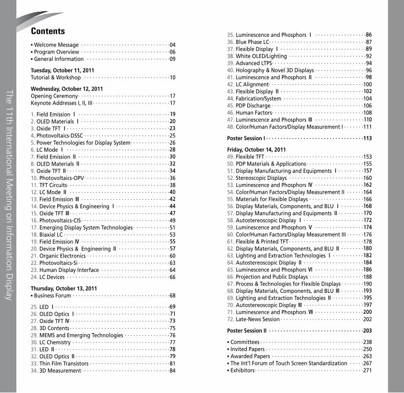
Welcome Message · · · · · · · · · · · · · · · · · · · · · · · · · · · · · · ·04 Program Overview · · · · · · · · · · · · · · · · · · · · · · · · · · · · · · ·06 General Information · · · · · · · · · · · · · · · · · · · · · · · · · · · · ·09
Tuesday, October 11, 2011Tutorial & Workshop · · · · · · · · · · · · · · · · · · · · · · · · · · · · · ·10
Wednesday, October 12, 2011Opening Ceremony · · · · · · · · · · · · · · · · · · · · · · · · · · · · · · · ·17Keynote Addresses I, II, III · · · · · · · · · · · · · · · · · · · · · · · · · · ·17
1. Field Emission Ⅰ · · · · · · · · · · · · · · · · · · · · · · · · · · · · · · · ·192. OLED Materials Ⅰ · · · · · · · · · · · · · · · · · · · · · · · · · · · · · · ·203. Oxide TFT Ⅰ · · · · · · · · · · · · · · · · · · · · · · · · · · · · · · · · · · · ·234. Photovoltaics-DSSC · · · · · · · · · · · · · · · · · · · · · · · · · · · · · ·255. Power Technologies for Display System · · · · · · · · · · · · · ·266. LC Mode Ⅰ · · · · · · · · · · · · · · · · · · · · · · · · · · · · · · · · · · · ·287. Field Emission Ⅱ · · · · · · · · · · · · · · · · · · · · · · · · · · · · · · · ·308. OLED Materials Ⅱ · · · · · · · · · · · · · · · · · · · · · · · · · · · · · · ·329. Oxide TFT Ⅱ · · · · · · · · · · · · · · · · · · · · · · · · · · · · · · · · · · · ·3410. Photovoltaics-OPV · · · · · · · · · · · · · · · · · · · · · · · · · · · · · ·3611. TFT Circuits · · · · · · · · · · · · · · · · · · · · · · · · · · · · · · · · · · · ·3812. LC Mode Ⅱ · · · · · · · · · · · · · · · · · · · · · · · · · · · · · · · · · · ·4013. Field Emission Ⅲ · · · · · · · · · · · · · · · · · · · · · · · · · · · · · · ·4214. Device Physics & Engineering Ⅰ · · · · · · · · · · · · · · · · · · ·4415. Oxide TFT Ⅲ · · · · · · · · · · · · · · · · · · · · · · · · · · · · · · · · · · ·4716. Photovoltaics-CIS · · · · · · · · · · · · · · · · · · · · · · · · · · · · · · ·4917. Emerging Display System Technologies · · · · · · · · · · · · ·5118. Biaxial LC · · · · · · · · · · · · · · · · · · · · · · · · · · · · · · · · · · · · ·5319. Field Emission Ⅳ · · · · · · · · · · · · · · · · · · · · · · · · · · · · · · ·5520. Device Physics & Engineering Ⅱ · · · · · · · · · · · · · · · · · ·5721. Organic Electronics · · · · · · · · · · · · · · · · · · · · · · · · · · · · ·6022. Photovoltaics-Si · · · · · · · · · · · · · · · · · · · · · · · · · · · · · · · ·6323. Human Display Interface · · · · · · · · · · · · · · · · · · · · · · · ·6424. LC Devices · · · · · · · · · · · · · · · · · · · · · · · · · · · · · · · · · · · ·66
Thursday, October 13, 2011 Business Forum · · · · · · · · · · · · · · · · · · · · · · · · · · · · · · · · · ·68
25. LED Ⅰ · · · · · · · · · · · · · · · · · · · · · · · · · · · · · · · · · · · · · · · ·6926. OLED Optics Ⅰ · · · · · · · · · · · · · · · · · · · · · · · · · · · · · · · · ·7127. Oxide TFT Ⅳ · · · · · · · · · · · · · · · · · · · · · · · · · · · · · · · · · · ·7328. 3D Contents · · · · · · · · · · · · · · · · · · · · · · · · · · · · · · · · · · ·7529. MEMS and Emerging Technologies · · · · · · · · · · · · · · · ·7630. LC Chemistry · · · · · · · · · · · · · · · · · · · · · · · · · · · · · · · · · ·7731. LED Ⅱ · · · · · · · · · · · · · · · · · · · · · · · · · · · · · · · · · · · · · · · ·7832. OLED Optics Ⅱ · · · · · · · · · · · · · · · · · · · · · · · · · · · · · · · · ·7933. Thin Film Transistors · · · · · · · · · · · · · · · · · · · · · · · · · · · ·8134. 3D Measurement · · · · · · · · · · · · · · · · · · · · · · · · · · · · · · ·84
35. Luminescence and Phosphors Ⅰ · · · · · · · · · · · · · · · · · ·8636. Blue Phase LC · · · · · · · · · · · · · · · · · · · · · · · · · · · · · · · · · ·8737. Flexible Display Ⅰ · · · · · · · · · · · · · · · · · · · · · · · · · · · · · ·8938. White OLED/Lighting · · · · · · · · · · · · · · · · · · · · · · · · · · ·9239. Advanced LTPS · · · · · · · · · · · · · · · · · · · · · · · · · · · · · · · · ·9440. Holography & Novel 3D Displays · · · · · · · · · · · · · · · · · ·9641. Luminescence and Phosphors Ⅱ · · · · · · · · · · · · · · · · · ·9842. LC Alignment · · · · · · · · · · · · · · · · · · · · · · · · · · · · · · · · ·10043. Flexible Display Ⅱ · · · · · · · · · · · · · · · · · · · · · · · · · · · · ·10244. Fabrication/System · · · · · · · · · · · · · · · · · · · · · · · · · · · ·10445. PDP Discharge · · · · · · · · · · · · · · · · · · · · · · · · · · · · · · · ·10646. Human Factors · · · · · · · · · · · · · · · · · · · · · · · · · · · · · · · ·10847. Luminescence and Phosphors Ⅲ · · · · · · · · · · · · · · · · ·11048. Color/Human Factors/Display Measurement I · · · · · · ·111
Poster Session I · · · · · · · · · · · · · · · · · · · · · · · · · · · · · · · · · ·113
Friday, October 14, 201149. Flexible TFT · · · · · · · · · · · · · · · · · · · · · · · · · · · · · · · · · ·15350. PDP Materials & Applications · · · · · · · · · · · · · · · · · · · ·15551. Display Manufacturing and Equipments Ⅰ · · · · · · · · ·15752. Stereoscopic Displays · · · · · · · · · · · · · · · · · · · · · · · · · ·16053. Luminescence and Phosphors Ⅳ · · · · · · · · · · · · · · · · ·16254. Color/Human Factors/Display Measurement II · · · · · ·16455. Materials for Flexible Displays · · · · · · · · · · · · · · · · · · ·16656. Display Materials, Components, and BLU Ⅰ · · · · · · · ·16857. Display Manufacturing and Equipments Ⅱ · · · · · · · · ·17058. Autostereoscopic Display Ⅰ · · · · · · · · · · · · · · · · · · · · ·17259. Luminescence and Phosphors Ⅴ · · · · · · · · · · · · · · · · ·17460. Color/Human Factors/Display Measurement III · · · · · ·17661. Flexible & Printed TFT · · · · · · · · · · · · · · · · · · · · · · · · · ·17862. Display Materials, Components, and BLU Ⅱ · · · · · · · ·18063. Lighting and Extraction Technologies Ⅰ · · · · · · · · · · ·18264. Autostereoscopic Display Ⅱ · · · · · · · · · · · · · · · · · · · · ·18465. Luminescence and Phosphors Ⅵ · · · · · · · · · · · · · · · · ·18666. Projection and Public Displays · · · · · · · · · · · · · · · · · · ·18867. Process & Technologies for Flexible Displays · · · · · · · ·19068. Display Materials, Components, and BLU Ⅲ · · · · · · · ·19369. Lighting and Extraction Technologies Ⅱ · · · · · · · · · · ·19570. Autostereoscopic Display Ⅲ · · · · · · · · · · · · · · · · · · · · ·19771. Luminescence and Phosphors Ⅶ · · · · · · · · · · · · · · · · ·20072. Late-News Session · · · · · · · · · · · · · · · · · · · · · · · · · · · · ·202
Poster Session II · · · · · · · · · · · · · · · · · · · · · · · · · · · · · · · · ·203
Committees · · · · · · · · · · · · · · · · · · · · · · · · · · · · · · · · · · · ·238 Invited Papers · · · · · · · · · · · · · · · · · · · · · · · · · · · · · · · · · ·250 Awarded Papers · · · · · · · · · · · · · · · · · · · · · · · · · · · · · · · ·263 The Int’l Forum of Touch Screen Standardization · · · · ·267 Exhibitors · · · · · · · · · · · · · · · · · · · · · · · · · · · · · · · · · · · · · ·271
Contents
The 11th International Meeting on Inform
ation Display
The 11th International Meeting on Information Display4 October 11-15, 2011 5
Welcome to the 11th International Meeting on Information Display IMID 2011!
On behalf of the Organizing Committee of the IMID 2011, it is our great pleasure to welcome keynote and invited speakers, participants, and guests to the conference. We would also like to express our deepest gratitude to all paper presenters to this year’s IMID held at KINTEX in Seoul, Korea, during October 11 to 15, 2011.
IMID conference has substantially grown since established 11 years ago and it has also been serving as a premiere gathering ground for the world’s most talented representatives within the information display industries, universities, and research laboratories. In each year, over 2,000 delegates participate in this event with over 400 distinguished papers presented. The growth of IMID indeed contributed to development of the display industry in Korea. The presence of so many prominent industry forces allows the conference not only to feature tangible examples generated from the industry’s leading edge but also to enhance great academic insights through them.
In the industry currently undergoing the rapid progress, there are many compelling topics that require incisive discussions and commentaries. Against the backdrop, in this year’s IMID conference, three renowned experts will share their knowledge in the Keynote Speeches; Dr. Seungkwon Ahn, President & CTO of LG Electronics, Inc., Korea on “Value Innovation with 3D Technology (Futuristic 3D Technology)”, Dr. David Morton, Program Manager of the Army Research Laboratory in USA on “Flexible Display Development”, and Dr. Johan Feenstra, CEO of Samsung LCD Netherlands, R&D Center BV in the Netherlands on “Merging eReaders and Tablets with Liquavista Technology”.
The IMID 2011 contains 447 papers selected from 17 countries and this number includes 112 invited papers based on the general topic of displays within the related fields. The fabulous findings will be presented throughout 72 sessions prepared and the two poster sessions.
On the top of the outstanding technical program, the IMID 2011 will feature a wide variety of workshops and tutorials which provide attendees a chance to share information on extensive arrays of topics. This year’s tutorial and workshops will be held under the topics of 3D Display, Oxide TFT, OLED Lighting and AMOLED for TV.
In addition, the Business Forum co-organized by DisplaySearch, will enable participants to analyze display market issues and, simultaneously, explore potential value creation opportunities. Moreover, exhibitions held during the IMID 2011 are co-organized by Korea Display Industry Association and include prominent companies such as Merck, LG Display Co., Ltd., Samsung Electronics Co., Ltd. It is anticipated to attract an impressive number of participants as the exhibitors gathered to display their cutting-edge products, materials, and equipments to introduce and promote.
As mentioned earlier, the IMID 2011 will be held in Seoul, the most fascinating and dynamic venue in Korea. The venue embraces numerous historical monuments and culture relics as well as modernized shopping centers. It will, therefore, provide participants a chance to experience the vivid Korean culture as well as the life style.
For such a successful conference, all members of the Organizing Committee of the IMID 2011 have exerted every effort, and the conference sponsors have also generated invaluable contributions toward the conference. We, once again, express our deepest gratitude for your excellent endorsement and contributions.
We truly hope you enjoy the most of both technical and social programs prepared for you and look forward to welcoming you to Korea!
Thank you.
Sincerely yours,
Welcome Message
Ki-Woong WhangGeneral Co-Chair
Director of SID Korea ChapterSeoul Nat’l Univ.
Oh-Kyong Kwon General Chair
President of KIDSHanyang Univ.

The 11th International Meeting on Information Display6 October 11-15, 2011 7
Program OverviewProgram Overview
Tutorial & Workshop Tuesday, October 11, 2011, 10:00 ~ 17:40, Room 305 & 306
TutorialⅠ: OLED Lighting (Room 306)10:00 ~ 10:50 Material and Devices Technologies for OLED Lighting Jang Hyuk Kwon (Kyung Hee Univ., Korea)
10:50 ~ 11:40 Enhancement of Out-Coupling Efficiency in OLEDs Min Cheol Oh (Pusan Nat’l Univ., Korea)
11:40 ~ 12:30 International Standardization of OLED Lighting in IEC Doo-Hee Cho (ETRI, Korea)
Tutorial Ⅱ: 3D Display I (Room 305)14:40 ~ 14:50 Holographic 3D Projection Imaging Hwi Kim (Korea Univ., Korea)
14:50 ~ 15:40 3-D Standardization Nam Kim (Chungbuk Nat’l Univ., Korea)
Workshop I : Oxide TFT I (Room 305)10:00 ~ 10:50 Oxide TFT Technology Sang-Hee Ko Park (ETRI, Korea)
10:50 ~ 11:40 Stability of Oxide TFTs Jae Kyeong Jeong (Inha Univ., Korea)
11:40 ~ 12:30 Issues on Oxide Semiconductor TFT Je-Hun Lee (Samsung Electonics Co., Ltd., Korea)
Workshop Ⅱ: 3D Display Ⅱ (Room 305)16:00 ~ 16:50 Full-Color 3D Display System Based on Electronic
Holography Kunihiro Sato (Hyogo Univ., Japan)
16:50 ~ 17:40 3D Disply using Electronic Holography and 3D Data Acquisition Using Ray-Based Image Sensors
Kenji Yamamoto (NICT, Japan)
Workshop Ⅲ: AMOLED for TV Ⅰ(Room 306)14:00 ~ 14:50 The Principle and R&D Trend of OLEDs: Materials and
Device Ruiqing (Ray) Ma (Universal Display Corp., USA)
14:50 ~ 15:40 OLED Patterning Technology Chang Wook Han (LG Display Co., Ltd., Korea)
Workshop Ⅳ: AMOLED for TV Ⅱ (Room 306)16:00 ~ 16:50 AMOLED Pixel Driving Techniques Hyoungsik Nam (Kyung Hee Univ., Korea)
16:50 ~ 17:40 [Tutorial] 3D AMOLED Hee-Jin Choi (Sejong Univ., Korea)
Opening Ceremony Wednesday, October 12, 2011, 08:40 ~ 09:00, Event Hall 6C, 1F
Keynote Addresses Wednesday, October 12, 2011, 09:00 ~ 10:30, Event Hall 6C, 1F
Business Forum Thursday, October 13, 2011, 09:00 ~ 18:00, Room 401 + 402
IMID Business Forum 2011 will take place on October 13, 2011 in the KINTEX, Korea, co-organized by DisplaySearch Korea and KIDS (The Korea Information Display Society). Attendees will gain accurate market analysis including future plans from leading flat panel companies’ insight in the worldwide FDP market with the latest DisplaySearch industry forecasts and numerous networking opportunities.
Keynote IValue Innovation with 3D Technology (Futuristic 3D Technology)
Dr. Seungkwon AhnPresident & CTO, LG Electronics Inc., Korea
Keynote IIFlexible Display Development
Dr. David MortonProgram manager, The Army Research Laboratory, USA]
Keynote IIIMerging eReaders and Tablets with Liquavista technology
Dr. Johan FeenstraCEO, Samsung LCD Netherlands R&D Center BV., The Netherlands
The 11th International Meeting on Information Display8
Program Overview
October 11-15, 2011 9
General Information
Exhibition Wednesday ~ Friday, October 12 ~ 13, 2011, KINTEX 1 Hall
The IMID 2011 opens along with the Korea Electronic Show (KES). The Show features exhibitions and seminars on semiconductors, consumer electronics, and telecommunications. This new format will provide IMID 2011 participants with greater opportunities to experience and discuss state-of-the-art information display technologies. Please take this opportunity to enjoy informative discussion with exhibitors.
Banquet Thursday, October 13, 2011, 19:00 ~ 21:00
• Location: Grand Ballroom, Grand Hilton Seoul• Fee: USD 60• The Free Shuttle bus will be operated from KINTEX to Grand Hilton Seoul
Awards • Award of Minister of Education, Science and Technology• Merck Grand Awards• Merck Young Scientist Awards• KIDS Awards (Sponsored by LG Display)*• KIDS Awards (Sponsored by Samsung Electronics)*
The Awardees have been selected from papers submitted to IMID 2011 based upon their originality and the technical significance to information display industry. The Awards will be presented at the Banquet on Thursday, October 13, 2011, at the Grand Hilton Seoul.* These awards were given at the “Day of Display” on October 4, 2011.
Presentation Time for Speakers - Keynote: 30 min.- Tutorial & Workshop: 50 min.- Invited: 20 minutes for presentation and 5 minutes for Q&A- Oral: 15 minutes for presentation and 5 minutes for Q&APreview Room
Preview Room For speakers a slide preview room will be available at the Room 307A, 3F.
Registration Desk Hours The IMID 2011 Registration Desk will be located at the 2F, KINTEX Ⅱ. You can register on-site during the hours listed below.
• Tuesday, October 11, 2011 ··············································· 09:00 ~ 18:00• Wednesday, October 12, 2011 ········································· 07:30 ~ 18:00• Thursday, October 13, 2011 ············································· 08:00 ~ 18:00• Friday, October 14, 2011 ·················································· 08:00 ~ 18:00
Clock Room A clockroom including a luggage storage area is located next to 307A.
Internet Lounge The Internet Lounge, sponsored by LG Electronics Inc. is located at the front of the Room 301 & 302. You can bring your own lab-top computer for Internet connection or use the computers in the Internet Lounge with high-speed access.
Conference Language The official language of the conference is English.
The 11th International Meeting on Information Display10 October 11-15, 2011 11
Tutorial & WorkshopTutorial & Workshop
Tutorial I Chair: Dr. Hye Yong Chu (ETRI, Korea)
OLED Lighting
[T1-1] 10:00Material and Devices Technologies for OLED LightingJang Hyuk Kwon (Kyung Hee Univ., Korea)
OLED lighting has made strong advances over the past few years. It is anticipated delivering strong impact on energy and the environment fields. However, OLED lighting still faces many technical and non-technical challenges before it can become a successful commercial product. This tutorial will address the basic principles, current technical status, and challenged technologies based on material and device viewpoints.
[T1-2] 10:50Enhancement of Out-Coupling Efficiency in OLEDsMin Cheol Oh (Pusan Nat'l Univ., Korea)
Extraction of the captured light inside the OLED device is an important issue to improve the power efficiency and increase the life time. In ordinary OLED structure, only 20% of the created light from the exiton is coupled out of the device to become useful. In terms of the modification of the OLED device structure, various approaches have been reported to improve the efficiency of outcoupling. This tutorial presentation will cover the reason of internal light capturing, the recent progress of the outcoupling enhancement research, and the method how to design the optical structure in OLEDs.
Tuesday, October 11, 2011 / 10:00 ~ 17:40 Room 305 & 306Tuesday, October 11, 2011 / 10:00 ~ 17:40 Room 305 & 306
[T1-3] 11:40International Standardization of OLED Lighting in IECDoo-Hee Cho (ETRI, Korea)
A technical standard is an established norm or requirement about technical systems. The international standard for OLED lighting is required for its speciality in electrical and photonic characteristics d International Electrotechnical Commission (IEC) is the leading global organization that publishes International Standards, founded in 1906. The international standard for lighting technology is dealt in IEC TC34. The standard draft for safety requirements of OLED lighting panel is now being prepared and performance requirements of it will be discussed in the near future in IEC TC34 PRESCO OLED PT.
Tutorial II Chair: Dr. Sung Kyu Kim (KIST, Korea)
3D Display Ⅰ
[T2-1] 14:00Holographic 3D Projection ImagingHwi Kim (Korea Univ., Korea)
Holographic 3D display technology attracts strong research interest recently. Holographic 3D display is considered as the ultimate realization of 3D displays which can reconstruct the almost same light fields as the natural image light fields of real or virtual 3D objects. In this tutorial, the key elements of holographic 3D display technology are broadly reviewed. Recent progresses, theoretical models, and practical implementation of holographic 3D displays are included. Scalar wave optic model of observation of 3D objects is presented with simulation results. Projection-type holographic 3D display and hybrid-type holographic display are analyzed comparatively. In particular, technologies of light field modulation are introduced and the possible way to realize challenging complex light field modulation is discussed.
The 11th International Meeting on Information Display12
Tutorial & Workshop
October 11-15, 2011 13
Tutorial & Workshop
Room 305 & 306Room 305 & 306 Tuesday, October 11, 2011 / 10:00 ~ 17:40Tuesday, October 11, 2011 / 10:00 ~ 17:40
[W1-2] 10:50Stability of Oxide TFTsJae Kyeong Jeong (Inha Univ., Korea)
In this workshop, the device reliability including gate bias, thermal, and light-induced instability in the oxide TFTs will be addressed, which is one of the most critical issue for the oxide TFTs to be adopted for the advanced flat panel display. In particular, the plausible degradation mechanisms of the oxide TFTs under the bias and light illumination stress will be reviewed, which includes the oxygen vacancy model, hole trapping model and ambient-related dynamical reaction. Finally, the strategies for improving the stability of oxide TFTs will be suggested based on the proposed mechanism framework.
[W1-3] 11:40Issues on Oxide Semiconductor TFTJe-Hun Lee (Samsung Electonics Co., Ltd., Korea)
Amorphous oxide semiconductor (AOS) exhibited the characteristics of low fabrication costs by using pre-established a-Si:H TFT production line with minor modification, low off-current, and high mobility (>10 V-1s-1). Through these properties, the AOS TFTs showed the advantage to apply in the low power LCD Displays, high resolution 3D LCD TV, AMOLED TV displays, and flexible displays. Achieving high speed TFT with low off current is main issues to develop AOS. However, one of critical factors of IGZO TFTs in applications and mass production is the reliability and uniformity—the stability and uniformity of threshold voltage (Vth). Moreover, main parameters affecting threshold voltage of AOS TFTs are reviewed according to fabricatio process and oxide semiconducting material itself.
[T2-2] 14:503-D StandardizationNam Kim (Chungbuk Nat'l Univ., Korea)
Recently, 3-D(three-dimensional) display is a hot issue in the flat panel, game, cinema and medical industries. Stereoscopic and auto-stereoscopic display are now commercially released by many companies. Owing to the different 3-D methods, they cause many diverse performances and specifications which make an effect to human perception directly. So we need the standardizations to evaluate the 3-D display products. This tutorial introduces the recent progress of 3-D standardization of stereoscopic and auto-stereoscopic display, especially optical measurement methods for 3-D display. Current issues of the international standardization activities on stereoscopic, auto-stereoscopic and human factor will be presented. Also the activities including 3-D video, 3-D movie and 3-D broadcasting will be discussed.
Workshop I Chair: Prof. Byung Seong Bae (Hoseo Univ., Korea)
Oxide TFT Ⅰ
[W1-1] 10:00Oxide TFT TechnologySang-Hee Ko Park (ETRI, Korea)
Oxide TFTs have been intensively developed for the application of the backplane for large size TFT-LCD and AMOLED, flexible display, and transparent displaydue to their properly combined performances of high mobility and stability, large area uniformity, simple process, and transparency. Here, we reviewrecent development of oxide TFT and issues to be considered to get high performance. We also introduce the promise of oxide TFT for the application to the high resolution mobile display.
The 11th International Meeting on Information Display14
Tutorial & Workshop
Tuesday, October 11, 2011 / 10:00 ~ 17:40
October 11-15, 2011 15
Tutorial & Workshop
Tuesday, October 11, 2011 / 10:00 ~ 17:40Room 305 & 306 Room 305 & 306
Workshop III Chair: Prof. Min Chul Suh (Kyung Hee Univ., Korea)
AMOLED for TV I
[W3-1] 14:00The Principle and R&D Trend of OLEDs: Materials and DeviceRuiqing (Ray) Ma (Universal Display Corp., USA)
This workshop will begin with a brief history of OLEDs and the fundamental physics of standard device operation. This will be followed by more detailed discussion of device architecture and materials development with a strong focus on high-efficiency phosphorescent devices. Finally the R&D trend of OLEDs which includes AMOLED TV, flexible AMOLED displays, and OLED lighting will be discussed.
[W3-2] 14:50OLED Patterning TechnologyChang Wook Han (LG Display Co., Ltd., Korea)
OLED Patterning technology is crucial for the fabrication of AMOLED displays. This tutorial includes the conventional fine metal mask technology and other patterning technologies, including the white OLED with color filters, the laser patterning process, and the solution process. Patterning technology with high scalability, such as the white OLED with color filters and the solution process, is required in large-sized applications. High resolution patterning technology, such as the laser patterning process, is required in mobile and smartbook applications.
Workshop II Chair: Prof. Byoungho Lee (Seoul Nat’l Univ., Korea)
3D Display Ⅱ
[W2-1] 16:00Full-Color 3D Display System Based on Electronic HolographyKunihiro Sato (Hyogo Univ., Japan)
A 3D display with a multi-channel liquid-crystal display (LCD) panel is developed for enlarging the visual field or the viewing zone. One-shot digital holography is also developed for recording moving color 3D images. Reconstructed full-color images had a large color gamut and exhibited fine color expression. The viewing-zone angle or the visual-field angle has been enlarged up to about 18 degrees by adopting a 6-channel LCD panel. One-shot digital holography has been developed for instantaneous recording of a moving 3D image. It is possible to realize real-time recording and display of moving 3-D images if RGB pulse lasers are adopted.
[W2-2] 16:503D Disply Using Electronic Holography and 3D Data Acquisition Using Ray-Based Image SensorsKenji Yamamoto (NICT, Japan)
This paper introduces two 3D visual systems using ray-based image sensors and electronic holography display toward ultra-realistic communication. The first system uses integral photography for the capture of ray information at slightly separated locations. The second system uses camera array that includes 25 cameras to capture ray information at further locations than integral photography.Both systems use electronic holography as an ideal 3D display. Since spatial light modulators are currently inadequate specifications for electronic holography, the setup to remove disturbing light is necessary, which we implemented in both systems.Finally, I will glance at the topic of the new system using 300 cameras.
The 11th International Meeting on Information Display16
Tutorial & Workshop
Tuesday, October 11, 2011 / 10:00 ~ 17:40
October 11-15, 2011 17
Hall 6CRoom 305 & 306
Workshop IV Chair: Prof. Min Chul Suh (Kyung Hee Univ., Korea)
AMOLED TV II
[W4-1] 16:00AMOLED Pixel Driving TechniquesHyoungsik Nam (Kyung Hee Univ., Korea)
The market share of AMOLED has been significantly on the increase in the arena of small display applications including mobile phones, which is highly likely expected to expand its domain into TV applications down the road on the back of wide color gamut, slim & light design, high contrast ratio, fast response time, and the like. However, AMOLED TVs must cope with several issues for mass-production. We will take a look at those issues and address compensation techniques against them.
[W4-2] 16:503D AMOLEDHee-Jin Choi (Sejong Univ., Korea)
The progressives on the flat panel display (FPD) technology have made it possible to realize practical 3D displays using special glasses. Although the existing stereoscopic products adopts the binocular disparity as a common principle, the methods for realization depend on the kinds of FPD devices. In this session, the structures and principles of stereoscopic display including 3D AMOLED is introduced and compared with other stereoscopic displays.
Tuesday, October 12, 2011 / 08:40 ~ 09:00
Opening Ceremony
Chair: Tae-Hoon Yoon (Executive Committee Chair, Pusan Nat’l Univ., Korea)
- Opening Address: Oh-Kyong Kwon (General Chair, President of KIDS, Hanyang Univ., Korea) - Congratulatory Remark 1: Munisamy Anandan (President of SID, USA)
[Keynote I] 09:00
Value Innovation with 3D Technology (Futuristic 3D Technology)
Seungkwon Ahn (President & CTO, LG Electronics Inc., Korea)
In this keynote speech, the subjects of ‘Introduction of Next 3D Display Technology’ and ‘Value Proposition with 3D Technology’ will be dealt with to share the latest research outputs regarding the above. Details of ‘Introduction of next 3D Display Technology’ covering Glassless 3D, Auto Stereoscopic Display, Ultra Definition, Hologram Type, Real 3D and Large OLED TV, as well as ‘Value Proposition with 3D Technology’ including 3D TV, Mobile 3D and 3D projector will also be conveyed within the presentation.
Keynote Addresses
Wednesday, October 12, 2011 / 09:00 ~ 10:30 Hall 6C
Chair: Byoungho Lee (Program Committee Chair, Seoul Nat’l Univ., Korea)

The 11th International Meeting on Information Display18
Hall 6C
October 11-15, 2011 19
Room 301Wednesday, October 12, 2011 / 10:50 ~ 11:40
1. Field Emission Ⅰ
Wednesday, October 12, 2011 / 09:00 ~ 10:30
Keynote Addresses
[Keynote II] 09:30
Flexible Display Development
David Morton (Program manager, The Army Research Laboratory, USA)
Flexible Displays have been under development for number of years. The current technology demonstrators from a number of sources illustrate the promise of the technology and potential new applications. The development work ranges from individual researchers through development institutions and small companies to very large manufacturers. This talk will discuss the applications for the technology that includes portable rugged devices currently being demonstrated to futuristic applications as the technologies matures. The talk will include the state of manufacturing of flexible displays specifically fabrications of flexible active matrix backplanes.The talk will conclude with several of the key challenges for implementation of the technology into mainstream applications.
[Keynote III] 10:00
Merging eReaders and Tablets with Liquavista Technology
Johan Feenstra (CEO, Samsung LCD Netherlands R&D Center BV., The Netherlands)
In this presentation we will review current status of the markets for eReaders and for tablets. More specifically, the technologies used in these market areas will be discussed, with a focus on Liquavista technology. These electrowetting displays bring the best of both worlds together, combining low power and readability with video and color capability.
Chairs: Cheol Jin Lee (Korea Univ., Korea) Hidenori Mimura (Shizuoka Univ., Japan)
[1-1] 10:50 ~ 11:15
[Invited] Carbon Nanotube Cathode with Laser and High Electric Field Treatments for Field Emission Display
Mikio Takai, Tomoya Manabe, Tomoaki Takikawa, Hiroshi Oki, Satoshi Abo, and Fujio Wakaya (Osaka Univ., Japan)
Carbon nanotube (CNT) cathodes with high emission current and long lifetime have been realized using laser surface treatments and pulsed high electric field aging, resulting in the field emission lifetimes exceeded 100 hours in dc operation at 1 /, corresponding to 100,000 hours at a duty ratio of 1/1000.
[1-2] 11:15 ~ 11:40
[Invited] Field Emission Display with Printable Planar Triode
Wei Lei, Xiaobing Zhang, and Baoping Wang (Southeast Univ., China)
The principle of field-emission display is almost the same as the traditional cathode ray tube, so it should display the image with the same quality as CRT. However, the triode structure and uniformity of field-emission is two key issues regarding the field-emission display. In this paper, a planar triode is discussed deeply. The structure of this planar triode is quite simple, and it can be fabricated cheaply with screenprinting method. A prototype has been made to verify the concept of the printable field-emission triode.

The 11th International Meeting on Information Display20 October 11-15, 2011 21
Chair: Byung Doo Chin (Dankook Univ., Korea)
[2-1] 10:50 ~ 11:15
[Invited] New Blue Emitters and Hole Injection Materials Based on Organic Molecules for OLEDs
Beomjin Kim, Youngil Park, and Jongwook Park (The Catholic Univ. of Korea, Korea)
The molecular design and synthesis as well as the device performance of three categorized novel organic molecules for highly efficient blue emission and hole injection in OLEDs will be discussed. The first one is about the bulky side group effect. One of the synthesized blue emitting materials exhibited excellent color coordinates of (0.156, 0.088) and a luminance efficiency of 3.64 /A. The second one is a quite new core structure containing an indenopyrazine moiety which includes an imine group in the core structure. Furthermore, novel HIL compounds based on phenoxazine moiety as well as white OLED device fabricated by using new blue materials in spin-coating will be discussed.
[2-2] 11:15 ~ 11:40
[Invited] Novel Materials for New Design OLED
K. M. Fung, S. Y. Ching, and K. W. Cheah (Hong Kong Baptist Univ., Hong Kong)
The performance OLED can be enhanced by judicious design using novel materials. Thus the development of new materials is essential in continuing the design of better OLED. In this presentation, the principles characteristics of several new/critical materials; the doping of Cs2CO3 in electron injection material is one of the commonly adopted methods We investigated its chemical status when it is doped into electron transport materials. We also investigated doped metals as transparent electrode, characterizing their electrical and optical properties.
[2-3] 11:40 ~ 12:00
Solution Processed Multilayer Emitting Structure in Organic Light-Emitting Diodes Using an Alcohol Soluble Phosphorescent Emitting Layer
Kyoung Soo Yoo and Jun Yeob Lee (Dankook Univ., Korea)
Solution processed multilayer emitting structure blue phosphorescent organic light-emitting diodes (OLEDs) was developed using an alcohol soluble phosphine oxide type host material. 2-7-Bis(diphenylphosphoryl)-9,9’- spirobi(fluorene)(SPPO13) and iridium(III) bis(2-(4,6- difluorophenyl)-pyridinato-N,C2)picolonato(FIrpic) were used as alcohol soluble host and dopant material. Double emitting layer structure OLEDs and single emitting layer structure OLEDs with exciton blocking layer were fabricated and the device performances were investigated using alcohol soluble emitting material. The solution processed blue PHOLEDs showed a maximum quantum efficiency of 14.1% and high quantum efficiency of 11.0% at 1000 /.
[2-4] 12:00 ~ 12:20
ITO-Free Electrodes for OLED Devices Using Metal Nanowires and Hole-Injecting Polymer
Florian Pschenitzka (Cambrios Technologies Corp., USA), Mathew Mathai, Richard Tuttle, Eli Scott, and Robert Mitchell (Plextronics, Inc., USA)
We developed a solution-processable transparent conducting hole-injection anode for OLED applications.The electrode consists of two layers deposited by spincoating in separate processing steps. The first layer was deposited from aqueous dispersion of silver nanowires (Cambrios’ ClearOhm™ material) to form a transparentconductive network. A second layer was deposited to form a layer of layer of Sulfonated poly(thiophene-3-[2-(2- methoxyethoxy)ethoxy]-2,5-diyl) (Plextronic’s Plexcore® OC ink) with good hole-injecting properties.Both inks, silver nanowires as well as polythiophene, were optimized to achieve the required film planarity for OLED applications.OLED devices show similar efficiencies and lifetime characteristics compared to devices made with conventional ITO anode.
2. OLED Materials Ⅰ
Room 302Wednesday, October 12, 2011 / 10:50 ~ 12:40Room 302
2. OLED Materials Ⅰ
Wednesday, October 12, 2011 / 10:50 ~ 12:40

The 11th International Meeting on Information Display22 October 11-15, 2011 23
[2-5] 12:20 ~ 12:40
Using a High Glass Transition Temperature Hole Transport Material to Enhanced Thermal Stability and Efficiency of Organic Light-Emitting Diode
Kuang-Chih Lai, Lin-Ann Hong, Chang-Jun Lai (Nat’l Formosa Univ., Taiwan), Pei-Hsun Yeh (Raystar Optronics Inc., Taiwan), Shun-Hsi Wang, Fuh-Shyang Juang, and Yu-Sheng Tsai (Nat’l Formosa Univ., Taiwan)
Hole transport materials (HTG-1 and HTG-2) with high glass transition temperature (Tg) have been used to replace NPB to improve the thermal stability of organic light-emitting diodes (OLED). The method for detecting the degradation of organic film material, Tg of HTG-1 is 175~180 , in comparison with 155~160 for HTG-2. Using HTG-1 as a hole transport layer (HTL) and optimizing device structure, the luminance efficiency was 15 /A at 100 /. Furthermore, via the comparison of decay-ratio of luminance efficiency before and after a heating process, it has demonstrated that employing a high Tg organic material as HTL to improve the thermal stability of OLED can be achieved.
Chairs: Hyun Jae Kim (Yonsei Univ., Korea) Jae Kyeong Jeong (Inha Univ., Korea)
[3-1] 10:50 ~ 11:05
[Invited] Self-Aligned Top-Gate Oxide TFT Technology
Narihiro Morosawa, Yoshiyuki Oshima, Mitsuo Morooka, Toshiaki Arai, and Tetsuya Sasaoka (Sony Corp., Japan)
We developed a novel self-aligned top-gate oxide TFT for AM-OLED displays. Our developed Al reaction method to obtain source/drain regions is effective to fabricate a short channel and highly reliable TFT. A 9.9-inch diagonal qHD AM-OLED display was demonstrated to provide applicable solution for a large-sized and ultra-high definition OLED mass production.
[3-2] 11:05 ~ 11:30
[Invited] Highly Stable Oxide Semiconductor TFT Devices for Display Applications
Joon Seok Park, Tae Sang Kim, Kyoung Seok Son, Hyun-Suk Kim, Jong-Baek Seon, Myungkwan Ryu, and Sang Yoon Lee (Samsung Advanced Inst. of Tech., Korea)
The development of Hf-In-Zn-O thin-film transistor devices is presented. For the integration of such devices in next generation flat panel displays, it is necessary to achieve sufficient electrical performance and stability in terms of field effect mobility, and threshold voltage shifts upon negative bias illumination stress (NBIS). The enhancement of the TFT characteristics is achieved by the proper selection of gate insulators, semiconductor process and composition, and the adoption of relatively dense passivation layers.
Room 303Wednesday, October 12, 2011 / 10:50 ~ 12:10
3. Oxide TFT Ⅰ
Room 302Wednesday, October 12, 2011 / 10:50 ~ 12:40
2. OLED Materials Ⅰ
The 11th International Meeting on Information Display24 October 11-15, 2011 25
Room 306Wednesday, October. 12, 2011 / 10:50 ~ 12:10
4. Photovoltaics-DSSC
Room 303Wednesday, October 12, 2011 / 10:50 ~ 12:10
3. Oxide TFT Ⅰ
[3-3] 11:30 ~ 11:50
Highly Stable Amorphous Indium Gallium Zinc Oxide Thin-Film Transistors
Hoon Yim, Dae-Hwan Kim, SeungChan Choi, Byung Gook Choi, Sul Lee, Jong-Uk Bae, Chang-Dong Kim, Myungchul Jun, and Yong Kee Hwang (LG Display Co., Ltd., Korea)
Amorphous InGaZnO4 (a-IGZO) thin film transistors (TFTs) are promising devices in backplane technology.Since a-IGZO TFTs are very sensitive to the fabrication processes, they need a stable process. Herein we improved the stability of a-IGZO. The stability characteristic of a- IGZO TFT was improved with N2O plasma. Vth shift was 1.2V for 10,000s under NBTS with illumination.
[3-4] 11:50 ~ 12:10
High Mobility Ultrathin a-IGZO TFTs
Mallory Mativenga, Dong Han Kang, and Jin Jang (Kyung Hee Univ., Korea)
We have fabricated high-performance thin-film transistors (TFTs) incorporating 5 nm-thick amorphous-indium-gallium-zinc-oxide (a-IGZO) channel layers. The TFTs employ the bottom-gate inverted staggered structure with SiO2 gate-insulators and back-channel passivation. The field-effect mobility and gate-voltage swing are ~100 /V s and ~0.25 V/decade, respectively. Depending on the channel length, a depletion mode of operation is achieved with turn-on voltage ranging from ~-9 to -2 V. Threshold-voltage shifts under gate-bias stress of 20 V are <1 V after 104 s. Good stability and performance are attributed to a reduced number of defects in the ultrathin a-IGZO layer.
Chair: MunPyo Hong (Korea Univ., Korea)
[4-1] 10:50 ~ 11:15
[Invited] Solar Energy Conversion by Dye Sensitized Mesoscopic Systems
Md. K. Nazeeruddin (Swiss Federal Inst. of Tech., Switzerland)
Dye-sensitized solar cells (DSSC) consist of sensitizer derivatized mesoporous TiO2 film, and counter electrode, sand-witched with a hole transporting material or redox electrolyte. The immobilized sensitizer absorbs a photon to produce an excited state, which transfers efficiently its electron into the TiO2 conduction band. The oxidized dye is subsequently reduced by electron donation from the iodide/triiodide redox system. The injected electron flows through the semiconductor network to arrive at the back contact and then through the external load to the counter electrode. At the counter electrode, reduction of redox system completes the circuit. [1,2] In these cells nanocrystalline TiO2 film, the sensitizer and the redox couple are the key components for high power conversion efficiency. [3] This talk presents the state-of-the art of dye-sensitized solar cells and strategies for enhancing power conversion efficiencies above 13%.
[4-2] 11:15 ~ 11:35
RF Power Dependent Structural, Electrical and Optical Properties of ZnO:Al Thin Films Grown at Room Temperature
Bhaskar Chandra Mohanty, Byeong Kon Kim, Deuk Ho Yeon, Ik Jin Choi, Yeon Hwa Jo, Seung Min Lee, and Yong Soo Cho (Yonsei Univ., Korea)
Structural and optical properties of ZnO:Al thin films grown at room temperature by RF magnetron sputtering under various target powers have been investigated. A structural degradation characterized by large reduction of the (002) peak intensity and increased polycrystallinity, and progressive change from a columnar to a non-columnar and faceted microstructure with an increase in RF power have been observed. The resistivity decreased from 1.2 Ω at 50 W to 7.4 × 10⁻⁴ Ω at 200 W. Concurrently, the refractive index of the films decreased continuously owing to the increasing carrier concentration and decreasing packing density of the films.
Room 304

The 11th International Meeting on Information Display26 October 11-15, 2011 27
Chairs: Achintya Bhowmik (Intel Corp., USA) Jaehee You (Hongik Univ., Korea)
[5-1] 10:50 ~ 11:10
High Power-Efficient LED Backlight Driving System Independent of Forward Voltage Variation of LED for Large-Sized LCD Using Channel Reordering Method
Jae-Hun Ye, Ki-Soo Nam, Hyun-A Ahn, Young-Ho Jung, and Oh-Kyong Kwon (Hanyang Univ., Korea)
A new light emitting diode (LED) backlight driving system which controls the multi-channel LED backlight for large-sized liquid crystal display (LCD) is proposed. To maintain high power efficiency of LED backlight module in spite of forward voltage variation of LEDs in a channel (ΔVf.ch), the proposed system adopts channel reordering method. The proposed system is simulated by using 0.35µm Bipolar CMOS DMOS (BCD) process technology. Simulation results show that power efficiency is 90.66% in spite of 2.2V difference in ΔVf.ch between worst case channel and best case channel on 30% pulse width modulation (PWM) duty ratio.
[5-2] 11:10 ~ 11:30
Adaptive 1D Dimming Technique Compensating for Non-Uniform Side-Lit Backlight Profile
Seung-Ryul Kim, Kwang-Joon Kim, Jongbin Kim, Jong-Man Kim, and Seung-Woo Lee (Kyung Hee Univ., Korea)
This paper proposes an efficient1D dimming methodto preserve and enhance the image quality forlow power LCD operation. This work proposes a simple expression to emulate the backlight profile based on the measurement results. We demonstrate our technology on the modified 12.1”LCD panel with 8 LED blocks by adopting a spatial low-pass filter on theeach backlight level.
Room 305Wednesday, October 12, 2011 / 10:50 ~ 12:10
5. Power Technologies for Display System
[5-3] 11:30 ~ 11:50
Current Control in Active Matrix Organic Light Emitting Diode Displays with Current Feedback
Patrick Schalberger, Marcus Herrmann, and Norbert Fruehauf (The Univ. of Stuttgart, Germany)
In this paper, some aspects of current feedback in AMOLED displays are discussed. Different controller types are compared with respect to their time domain behavior and a new nonlinear integrating controller is proposed.
[5-4] 11:50 ~ 12:10
Intelligent Power Simulation Method Using Capacitor Charge/Discharge Phenomenon in High Resolution and Small Size TFT-LCD
Myung-Jong Park, Hak-Su Kim, Sang-Duk Jung, Sung-Ho Kim, and Byeong-Koo Kim (LG Display Co., Ltd., Korea)
The TFT-LCD has driven by voltage between pixel and vcom electrode. Pixel electrode voltage was generated by voltage change of data and gate line. TFT pixel has many parasitic capacitors as overlap of gate and SD line.Therefore, we can calculate the power consumption of LCD according to capacitor charge and discharge by changing of gate and data line voltage.The capacitor of one pixel is departmentalize and defined.We are considered swing frequency and voltage level of each capacitor. To make higher accuracy, the power consumption is divided by three parts, for gate, data and vcom, and each part is subdivided according to thebehavior state.The calculated power consumption has high accuracy less than about ±10% error rate as compare the simulation results with experimental data of 4.5”HD panel.
5. Power Technologies for Display System
Room 305Wednesday, October 12, 2011 / 10:50 ~ 12:10
The 11th International Meeting on Information Display28 October 11-15, 2011 29
Room 306Wednesday, October 12, 2011 / 10:50 ~ 12:15Wednesday, October 12, 2011 / 10:50 ~ 12:15
Chair: Seung Hee Lee (Chonbuk Nat’l Univ., Korea)
[6-1] 10:50 ~ 11:15
[Invited] Printable and Robust Liguid Crystal Modes for Flexible Displays
Soon-Bum Kwon (Hoseo Univ., Korea), Ji-Hoon Lee (Pusan Nat’l Univ., Korea), Burm-Young Lee (NDIS Corp., Korea), Zhe Hong, and Yan Jin (Hoseo Univ., Korea)
We report on two kinds of encapsulated LC modes, nematic and cholesteric LC capsule modes, applicable to high performance of robust flexible displays made by simple processes including printing process for LC layer formation. Nematic LC capsule mode enables us to achieve flexible displays with low driving voltage and high contrast in reflective mode as well as in transmissive mode. Cholesteric LC capsule mode can be applied to full color flexible reflective bistable displays with vivid colors. In this paper we describe the device structure, fabrication process and display performance of the flexible LCDs using two those modes.
[6-2] 11:15 ~ 11:35
Optical Characteristic Optimization of Transmissive Electrically Controlled Birefringence Mode LCD
Falu Yang, Junhwan Lim, Junrui Zhang, Yun Qiu, and Haigang Qing (Chengdu BOE Optoelectronics Tech. Co., Ltd., China)
Currently, display with high visual performance and low cost are main trend in smart mobile market, Normally white ECB mode LCD is an appropriate choice for it. To obtain the best optical characteristic of ECB LCD, we optimized several design factors such as compensation film in polarizer, nd of liquid crystal cell, alignment pre-tilt angle. Through these experiment results, when ECB panel with compensation film in polarizer, low nd (0.277) of liquid crystal cell, and higher pre-tilt angle of alignment material, we can obtain best optical performance. This optimized new design concept for normally white ECB mode LCD will bring many advantages in smart mobile field.
Room 306
6. LC Mode Ⅰ[6-3] 11:35 ~ 11:55
Comparison of In-Plane Switching Pixel Structures for High-resolution Display
Sang-Ho Kim, Chang-Jae Jang, Kwan Kim, Sang-Gul Lee, and Yong-Min Ha (LG Display Co., Ltd., Korea)
A 4.5-inch HD (720×RGB×1280, 326ppi) LTPS TFT-LCD has been fabricated using IPS pixel structure. To improve the color shift at oblique angle, and to optimize the pixel transmittance, we’ve successfully evaluated the performance of 2-pixel dual domain structure including conventional ones. We believe that this new pixel structure can be a good choice for high-resolution display in terms of transmittance, viewing-angle picture quality and power consumption.
[6-4] 11:55 ~ 12:15
Switching Characteristics of Cholesteric Liquid Crystal with Long-Pitch
Byung Wok Park, Ki-Han Kim, Zheng-Guo Shen, and Tae-Hoon Yoon (Pusan Nat’l Univ., Korea)
We propose a cholesteric liquid crystal (ChLC) device that reflects infrared light in the planar state by long-pitch structure. The proposed device can be operated in both the dynamic mode and the memory mode. Fast response in the dynamic mode can be obtained by switching between thehomeotropic state and the focal conic state.
6. LC Mode Ⅰ

The 11th International Meeting on Information Display30 October 11-15, 2011 31
Room 301Wednesday, October 12, 2011 / 13:30 ~ 14:40
Chairs: Kyu Chang Park (Kyung Hee Univ., Korea) Yasuhito Gotoh (Kyoto Univ., Japan)
[7-1] 13:30 ~ 13:55
[Invited] Field Emitter Technologies for Ultra Fine Imaging Devices
Hidenori Mimura, Yoichiro Neo, Toru Aoki (Shizuoka Univ., Japan), Tomoya Yoshida, and Masayoshi Nagao (AIST, Japan)
We have been investigating principle technology of an ultra fine field emission display (FED) and an ultra fine CdTe Xray image sensor for creating nanovision devices. For the ultra fine FED, we have developed a volcano-structured double-gated field emitter arras capable of focusing anelectron beam without serous reduction in emission current.For the ultra fine X-ray image sensor, we have proposed and demonstrated a novel CdTe X-ray sensor consisting of a CdTe diode and a field emitter array.
[7-2] 13:55 ~ 14:20
[Invited] Recent Development of Materials for FED Application
Zhuo Sun, Huili Li, Tao Feng, Zhejuan Zhang, Likun Pan, Yiwei Chen, Xianqin Piao, Xiaohong Chen, Xiaojun Wang, and Ting Lu (East China Normal Univ., China)
With development of the advanced nanostructure materials including carbon nanotubes (CNTs), graphene, silver nanowire(AgNWs), phosphors, to make high performance with low cost of field emission display (FED) devices become possible. The excellent electron emission properties and good electrical conductivity of CNTs and graphene films make them as the optimized FE cathode. High conductive AgNWs film can be used as either transparent conductive film for anode electrode, or as a cathode electrode by screen process at low temperature (below 300). Low voltage phosphor such as ZnAl2O4:Mn2+ is introduced for diode structure FED application, and RGB based FED module working below 300V is demonstrated.
7. Field Emission Ⅱ
Room 301Wednesday, October 12, 2011 / 13:30 ~ 14:40
7. Field Emission Ⅱ
[7-3] 14:20 ~ 14:40
Field Emission Properties of Carbon Nanotube Point Emitters
Dong Hoon Shin, Yenan Song, Yuning Sun, Ji Hong Shin, Guohai Chen, and Cheol Jin Lee (Korea Univ., Korea)
We fabricated CNT based point emitters by various methods using carbon nanotubes (CNTs). The CNT point emitter showed the high emission current and good emission stability. We suggest that tip sonication treatment is a very promising way to enhance the performance of CNT field emitters. We suggest that CNT point emitters can provide high performance field emitters for x-ray sources and e-beam sources.

The 11th International Meeting on Information Display32 October 11-15, 2011 33
Chairs: Jongwook Park (The Catholic Univ. of Korea, Korea) Do-Hoon Hwang (Pusan Nat’l Univ., Korea)
[8-1] 13:30 ~ 13:55
[Invited] Fluorescent OLEDs with High External Quantum Efficiency beyond Conventional Upper Limit
Yong-Jin Pu, Go Nakata, Jian-Yong Hu, Yusuke Yamashita, Kenta Kobayashi, Daisuke Yokoyama, Hisahiro Sasabe, and Junji Kido (Yamagata Univ., Japan)
Charge balance is an important prerequisite to get a high EQE in OLEDs. When we use NPD and Alq3 with a green dopant, EQE was around 3%, but when we optimized HTL and ETL materials, EQE dramatically increased over 7%.We achieved 7.5% and 8.2% EQE at 100 / in a green and blue fluorescent OLED, respectively, only by optimizing charge balance.
[8-2] 13:55 ~ 14:15
Enhanced Electroluminescence by Incorporating a Thermally Activated Delayed Fluorescence Material into Emitting Layer
Tetsuya Nakagawa (Kyushu Univ., Japan), Sung-Yu Ku, Ken-Tsung Wong (Nat’l Taiwan Univ., Taiwan), and Chihaya Adachi (Kyushu Univ., Japan)
An organic light emitting diode based on thermally activated delayed fluorescence (TADF) is produced using a spirobifluorene derivative having the donor-acceptor moieties as an emitter. The bipolar spirobifluorene (Spiro-CN) based device displayed a maximum luminance of 12,000 / at 15 V. Because of the significant contribution of TADF, the maximum external quantum efficiency, the maximum luminous efficiency and the maximum power efficiency of the bipolar spirobifluorene based device were found to be 4.4%, 13.5 /A and 13.0 /W, respectively.
Room 302Wednesday, October 12, 2011 / 13:30 ~ 15:00
8. OLED Materials Ⅱ
Room 302Wednesday, October 12, 2011 / 13:30 ~ 15:00
8. OLED Materials Ⅱ[8-3] 14:15 ~ 14:35
Simple Structure and High Efficiency Blue Phosphorescent OLEDs
Young Hoon Son, Jung Soo Park, Woo Sik Jeon, Dae Chul Lim, Yoo Jin Doh, and Jang Hyuk Kwon (Kyung Hee Univ., Korea)
We report high-efficiency phosphorescent blue OLEDs with an organic three stacked structure. Using a high-triplet-energy-hole transporting material of TAPC and a high-triplet-energy-electron transporting material of TmPyPB, the organic three stacked structure has been realized withthree new narrow band-gap blue host materials. These host materials have bipolar characteristics and high triplet energy of >2.8 eV. Very low onset voltages of 2.8~3.0V and driving voltages of 4.2~4.6V to obtain a brightness of 1000 /are achieved in this three stacked device configuration. Maximum external quantum efficiency above 20% is reported.
[8-4] 14:35 ~ 15:00
[Invited] Phosphorescent OLEDs: Enabling Energy Efficient Displays and Lighting
Ruiqing Ma, Peter A. Levermore, Alexey Dyatkin, Zeinab Elshenawy, Vadim Adamovich, Huiqing Pang, Raymond C. Kwong, Michael S. Weaver, Mike Hack, and Julie J. Brown (Universal Display Corp., USA)
In this paper wepresent data for stable and highly efficient red, yellow, green and light blue phosphorescent OLEDs. Wedescribe how these energy efficientmaterial systems can be used to save power and reduce heat generation in mobile productdisplays and TVs. We also describe how an all-phosphorescent material system has been used to demonstrate 15 x 15 OLED light panels with lifetime to LT70 up to 30,000 hrs and efficacy up to 62 /W at 1,000 / with extremely low operating temperature.
The 11th International Meeting on Information Display34 October 11-15, 2011 35
Chairs: Narihiro Morosawa (Sony Corp., Japan) Sang-Hee Ko Park (ETRI, Korea)
[9-1] 13:30 ~ 13:55
[Invited] Cu-Mn Alloy Electrodes on In-Ga-Zn-O Semiconductors for Back-Channel-Etched Thin Film Transistors
Junichi Koike and Pil Sang Yun (Tohoku Univ., Japan)
Cu-Mn alloy was deposited on amorphous In-Ga-Zn-O semiconductors. A reaction layer was formed in an interface region and acted as a heavily doped n+ layer. Back-channel-etched TFT structure were successfully fabricated by selective wet etching of the electrode and the channel layers, and exhibited excellent ohmic and TFT properties.
[9-2] 13:55 ~ 14:20
[Invited] Oxide TFTs for Transparent AMOLED
Chi-Sun Hwang, Sang-Hee Ko Park, Min Ki Ryu, Himchan Oh, Woo-Seok Cheong, Sung Mook Chung, Shinhyuk Yang, Doo-Hee Cho, OhSang Kwon, Eunsook Park, Jae Eun Pi, In Yong Eom, and Kyeong-Ik Cho (ETRI, Korea)
Highly transparent(~60%)3.5inch qVGA transparent AMOLED driven by oxide TFTs is developed. The performance and stability of oxide TFTs is enhanced by optimization of active layer and engineering of interfaces in TFTs. Transparent AMOLED driven by oxide TFTs could be used as “smart windows”with functionaltransparent electronic circuitswhich are also composed of transparentoxide TFTs.
Room 303Wednesday, October 12, 2011 / 13:30 ~ 15:00
9. Oxide TFT Ⅱ
Room 303Wednesday, October 12, 2011 / 13:30 ~ 15:00
9. Oxide TFT Ⅱ[9-3] 14:20 ~ 14:40
Double-Layered Ti/Si Barrier Metal for Oxide Semiconductor TFTs Facilitates 4-Mask Process
Aya Hino, Takeaki Maeda, Shinya Morita, and Toshihiro Kugimiya (Kobe Steel Ltd., Japan)
We demonstrate new barrier metal structure consisting of Ti/Si for source/drain Cu interconnections in oxide semiconductor TFTs. TEM and SIMS analyses reveal that the double-layered Ti/Si suppresses the reaction and interdiffusion at the interface after 300 annealing. The underlying Si layer is very useful for the etch stopper during wet etching for Cu/Ti layers. The oxide TFTs with the double-layered Ti/Si show good TFT characteristics. It is concluded that the present structure facilitates 4-mask process in the oxide TFTmanufacturing line.
[9-4] 14:40 ~ 15:00
Improvement in the Negative Bias Stability of Solution-Processed Zinc Tin Oxide TFTs by Optimizing the Prebake Temperature
Se Yeob Park, Hong Yoon Jung, Kwang Hwan Ji, Ji-In Kim, and Jae Kyeong Jeong (Inha Univ., Korea)
We investigated the effect of prebaking temperature on the negative bias stress instability of solution-processed zinc tin oxide thin film transistor. Although the ZTO TFT with a channel prebaked at 100 for 5 min exhibited the negative threshold voltage (ΔVth) of 0.89 V under the negative bias stress (NBS) condition, the 200-prebaked ZTO TFTs had the superior reliability (ΔVth≈ -0.34 V) under the identical NBS condition. It can be inferred that the prebaking at the higher temperature enhances the interdiffusion of ZnO and SnO2, leading to the smooth interface between the gate dielectric and the ZTO channel.

The 11th International Meeting on Information Display36 October 11-15, 2011 37
Chair: Md. K. Nazeeruddin (Swiss Federal Inst. of Tech., Switzerland)
[10-1] 13:30 ~ 13:55
[Invited] Semitransparent Organic Solar Cells
Xizu Wang, Ging Meng Ng, Jian Wei Ho (Inst. of Materials Research and Engineering, Singapore), Tam Hoi Lam, and Furong Zhu (Hong Kong Baptist Univ., Hong Kong)
Zinc phthalocyanine (ZnPc): fullerene (C60)-based organic solar cell with a transparent cathode of Ag/LiF/indium tin oxide (ITO) is demonstrated. The ITO top electrode was formed at room temperature. The performance of the semitransparent organic photovoltaic cells is optimized over the two competing parameter of power conversion efficiency (PCE) and optical transparency. Semitransparent bulkheterojunction ZnPc:C60 photovoltaic cells with an average transmission of more than 40% in the visible light region and a PCE of ~3.0% measured under simulated AM1.5G illumination of 100 mW/ were obtained.
[10-2] 13:55 ~ 14:15
Polymeric and Molecular Materials for Organic Bulk-Heterojunction Solar Cells
He Yan, Martin Drees, Zhihua Chen, and Antonio Facchetti (Polyera Corp., USA)
In this paper, we present molecular and polymeric materials suitable for organic bulk-hetero-junction solar cell fabrications. This first semiconductor is a high-mobility electron-transporting polymer, [P(NDI2OD-T2)], which exhibits excellent n-channel field-effect transistor mobility up to 0.8 /Vs and LUMO energy of ~-4.0 eV; therefore, it could provide a promising alternative to the commonly used fullerene-based acceptors in bulk-heterojunction solar cells. In the second part of this paper, we will present new low-bandgap molecular and polymeric donors enabling polymer bulk-heterojunction solar cells with >8% efficiencies.
Room 304Wednesday, October 12, 2011 / 13:30 ~ 14:35
10. Photovoltaics-OPV
Room 304Wednesday, October 12, 2011 / 13:30 ~ 14:35
10. Photovoltaics-OPV[10-3] 14:15 ~ 14:35
Small Molecular Bulk Heterojunction Solar Cells Using Alternative Thermal Deposition
Ji Whan Kim, Hyo Jung Kim, Tae-Min Kim (Seoul Nat’l Univ., Korea), Hyun Hwi Lee (Pohang Accelerator Lab., Korea), and Jang-Joo Kim (Seoul Nat’l Univ., Korea)
We propose a new method to form small molecule based bulk heterojunctions (BHJs) through alternative thermal deposition (ATD), which is a simple modification of conventional thermal evaporation. The formation of BHJs in copper(II) phthalocyanine (CuPc) and fullerene (C60) isconfirmed by grazing incidence small angle x-ray scattering (GISAXS) and UV-VIS absorption. The performance of organic solar cells (OSCs) using ATD was improved compared to co-deposited devices. Incorporation of a copper iodide (CuI) layer on ITO has improved the performance even more.

The 11th International Meeting on Information Display38 October 11-15, 2011 39
Chair: Reiji Hattori (ASTEC, Japan)
[11-1] 13:30 ~ 13:50
A Novel Amorphous Silicon TFT Gate Driver Circuit with Optimized Design for Integrated Display Panel Manufacturing
Po-Jui Lin, I-Hsiu Lo, Yiming Li, and Cheng-Han Shen (Nat’l Chiao Tung Univ., Taiwan)
In this work, we study an amorphous silicon TFT gate drive circuit for a large-size display panel and optimize its dynamic characteristics using a simulation-based evolutionary methodology. Simulation results first reveal the interesting specification of the optimized circuit. For exploring the performance fluctuation resulting from process variation, the sensitivity analysis is t h u s introduced. Finally, the optimized circuit is fabricated and the measurement results not only meet the target but also show a high practicability of the achieved design.
[11-2] 13:50 ~ 14:10
N-Channel TFT Logic Gates with Full Output Voltage Swing
Tao Ren, HongKyun Leem, Jisun Kim, YounKyung Kim, JoonDong Kim, HwanSool Oh (Konkuk Univ., Korea), JaeEun Pi, Shinhyuk Yang, Min Ki Ryu, Sang-Hee Ko Park, Byounggon Yu (ETRI, Korea), KeeChan Park (Konkuk Univ., Korea)
N-channel TFT-based NAND and NOR gates with full output voltage swing are reported. The circuits use asymmetric feed-through of input signal transition and bootstrapping effect. The output pull-up TFT is strongly turned on by bootstrapping and completely turned off by input signal. Therefore the output voltage swing is same with the input signal. The operations of the logic gate circuits are confirmed by experimental results.
Room 305Wednesday, October 12, 2011 / 13:30 ~ 14:50
11. TFT Circuits
Room 305Wednesday, October 12, 2011 / 13:30 ~ 14:50
11. TFT Circuits[11-3] 14:10 ~ 14:30
Design for Less Stress in the Pull-Down Transistors for On-Panel TFT Gate Drivers
Nan Xiong Huang, Miin Shyue Shiau, Po Hung Chen, Hong-Chong Wu, Heng-Shou Hsu, and Don Gey Liu (Feng Chia Univ., Taiwan)
In this paper, we propose a novel gate driver by low-stress driven technique. In order to increase the lifetime of gate driver, we usually add the number of pull-down transistors. But it would increase the area and complexity of the gate driver circuit. Using the low-stress driven technique and dual pull-down structure could have the same lifetime of circuit. But, the novel gate driver could significantly reduce the circuit area.
[11-4] 14:30 ~ 14:50
Low Power Consumption Shift Register Using Depletion Mode Amorphous In-Ga-Zn-O TFTs
Seung-Jin Yoo, Jin-Seong Kang, and Oh-Kyong Kwon (Hanyang Univ., Korea)
A new shift register using amorphous In-Ga-Zn-O (a-IGZO) thin-film transistors (TFTs) with negative threshold voltage (VT) is presented. To achieve low power consumption, a DC signal is applied to the drain of pull-up TFTs in the output stage rather than a clock signal in the proposed shift register. The proposed circuit is simulated on 5-inch (XGA) panel condition and achieved that the power consumption of 10 stage shift register is 84.7 at the operating frequency of 46 KHz, and the circuit is successfully operated when VT of a-IGZO TFTs is -5 V.
The 11th International Meeting on Information Display40 October 11-15, 2011 41
Chairs: Yoonseuk Choi (Hanbat Nat’l Univ., Korea) Andy Y.-G. Fuh (Nat’l Cheng Kung Univ., Taiwan)
[12-1] 13:30 ~ 13:55
[Invited] Polarizer Free Reverse-Mode Liquid Crystal Gels with Super Twisted Orientation
Rumiko Yamaguchi, Koichiro Goto (Akita Univ., Japan), and Oleg Yaroshchuk (NASU, Ukraine)
Reverse-mode films of anisotropic gels with 270° super twisted molecular orientation have been prepared based on nematic liquid crystal MLC-6080 and a small amount of reactive mesogen RM-256. The samples with a contrast ratio of about 8 and a driving voltage less than 8 V have been obtained. The driving voltage was reduced to 4 V by lowering power of UV irradiation used to polymerize the reactive mesogen.
[12-2] 13:55 ~ 14:20
[Invited] Development of Push-Pull VA Mode with Simple Process and Low Material Cost
Chao Ping Chen, Yanbing Qiao, Lili Liu, Chia-Te Liao, Yu-Wen Chiu, Te-Chen Chung, and Tean-Sen Jen (Infovision Optoelectronics Co. Ltd., China)
Over past few years, with the motivation of developing a high-performance and low-cost wide viewing angle technology, we had made great effort in improving our proprietary vertical alignment mode, code-named as CVA. The latest CVA-III, with its novel push-pull electrode structure, not just simplifies the fabrication process but saves the material cost, while preserving a superior performance.
Room 306Wednesday, October 12, 2011 / 13:30 ~ 15:00
12. LC Mode Ⅱ[12-3] 14:20 ~ 14:40
Domain-Divided Twisted Nematic Liquid Crystal Mode Using Homeotropic Reactive Mesogen Mixture
Tae-Min Kim, You-Jin Lee, Yeon-Kyu Moon, Soo In Jo, Chang-Jae Yu, and Jae-Hoon Kim (Hanyang Univ., Korea)
We proposed the domain-divided twisted nematic liquid crystal (DDTN-LC) mode induced by four splayed TN structures in each sub-pixel. The four splayed TNs were simply obtained by the perpendicular assemble of the rubbed substrates with different pre-tilt angles. For the control of pre-tilt angles, reactive mesogen mixture was used to control the pre-tilt angles.
[12-4] 14:40 ~ 15:00
Color Dual-Frequency Cholesteric Displays with Direct Switching between the Planar and Focal Conic States
Wei Lee and Feng-Ching Lin (Chung Yuan Christian Univ., Taiwan)
We report on our design of a fast-response reflective display based on three dual-frequency cholesteric liquid crystals to individually yield R, G and B colors. Direct switching from the focal conic to the planar state isdemonstrated. Based on the ability of reversibly direct switching between these two stable states, drive schemes are thus conceived for the fast-response color display.
Room 306Wednesday, October 12, 2011 / 13:30 ~ 15:00
12. LC Mode Ⅱ
The 11th International Meeting on Information Display42 October 11-15, 2011 43
Chairs: Mikio Takai (Osaka Univ., Japan) Young-Rae Cho (Pusan Nat’l Univ., Korea)
[13-1] 15:10 ~ 15:35
[Invited] Hafnium Nitride Thin Film Cold Cathode for Field Emitter Arrays
Yasuhito Gotoh and Hiroshi Tsuji (Kyoto Univ., Japan)
Hafnium nitride thin films were prepared by rf magnetron sputtering in order to investigate their properties as a cold cathode material. Work function, electrical resistivity, and oxidation resistance at elevated temperatures were investigated and the properties were compared with those of the other transition metal nitrides. As a result, hafnium nitride films showed the relatively low work function, the lowest electrical resistivity, and the best performance against oxidation. A field emitter array with hafnium nitride cathode yielded a current of more than 1.5 . The current could be maintained for over 100 h.
[13-2] 15:35 ~ 16:00
[Invited] Application of One-Dimensional Nanomaterial Field Emitter in Field Emission Display
Jun Chen, Shaozhi Deng, Ningsheng Xu, Jie Luo, Liyuan Liu, Guofu Zhang, Yanlin Ke, Baohong Li, Yuxiang Chen, Kai Huang, Jian Chen, and Gengxing Liu (Sun Yat-Sen Univ., China)
One dimensional nanomaterials possess excellent field emission properties and have great potential applications in field emission display. In this talk we will introduce our recent progresses on field emission display using one-dimensional nanomaterial field emitters. Two different approaches have been employed to integrate one-dimensional nanomaterial field emitters into FED device. One uses a double-gate driving scheme, in whichseparated gate structure is used and thus nanomaterials prepared under high temperature could be employed. In another approach, the nanowire field emitters were directly integrated with gated structure. The device structure, fabrication process and performance of FED prototypes using these structures will be given.
Room 301Wednesday, October 12, 2011 / 15:10 ~ 16:20
13. Field Emission Ⅲ
[13-3] 16:00 ~ 16:20
Fabrication of High Efficient Field Emission Lamp with Carbon Nanotube Emitters
Hee Chul Woo, Su Woong Lee, Eun Hye Lee, An Na Ha, Woo Mi Bae, Young Ju Eom, Jin Jang, and Kyu Chang Park (Kyung Hee Univ., Korea)
We fabricated a carbon nanotube(CNT)-based triode field emission lamp with high brightness and efficiency. This triode structure is composed of a bridge gate, a bridge anode and a cathode. As a cathode, robust CNT emitters were formed by resist assisted patterning (RAP) method. Through this triode structure the anode voltage was applied over 30 without arcing. The measured anode current and the cathode current were comparable and leakage current to the gate electrode was ignorable. This enables us to achieve high efficiency in lamp application. Triode structure for field emission lamp was first investigated by simulation. Improved field emission characteristic of our CNT emitters and optimized triode structure can provide high efficient field emission lamp.
13. Field Emission Ⅲ
Wednesday, October 12, 2011 / 15:10 ~ 16:20 Room 301

The 11th International Meeting on Information Display44 October 11-15, 2011 45
Chairs: Jang Hyuk Kwon (Kyung Hee Univ., Korea) Yongsup Park (Kyung Hee Univ., Korea)
[14-1] 15:10 ~ 15:35
[Invited] Considerations in Designing Efficient Organic Light Emitting Diodes at High Brightness
Z. B. Wang, M. G. Helander, J. Qiu, and Z. H. Lu (Univ. of Toronto, Canada)
Single hole transport layer (HTL) with very large highest occupied molecular orbital (HOMO) is used to replace the traditional “step-wise” device design in organic light emitting diodes (OLEDs), which suppresses the exciton quenching caused by the accumulated cations. As a result, the device performance, especially at high luminance, is significantly enhanced. Chlorinated indium tin oxide (Cl-ITO) with very high work function (>6.1 eV) has been shown to enable the direct hole injection into the high HOMO HTL, which further simplify the device structure as additional layers of high work function transition metal oxides are not needed to assist in hole injection.
[14-2] 15:35 ~ 16:00
[Invited] Applications and Physics of Transition Metal Oxides for Organic Light-Emitting Devices
Wolfgang Kowalsk, Sami Hamwi, Katrin Schultheiß, Daniela Donhauser, and Michael Kröger (Technische Universität Braunschweig, Germany)
Transition metal oxides can be used as anode buffer layer or p-dopant in organic light emitting diodesandsignificantly enhance the device performance by lowering the driving voltage. We find very deep-lying energy levels –the work function can reach values of 6.8 eV-in transition metal oxide thin films and show, that in the metal oxide itself, charge transport is dominated by electrons (n-type).When the metal oxides are used as anode buffer on the layer, hole injection is enhanced by loweringthe injection barrier by 0.4 eV compared to an indium tin oxide anode.The very deep lying unoccupied states facilitate charge separation at the interface between transition metal oxide and hole-transporting layer. This effect accounts for the possibility of stacking highly efficient organic light emitting diodes. Another effect related to the deep unoccupied states in MoO3 is the possibility of p-doping of organic wide band gap materials such as CBP or a-NPD.
Room 302Wednesday, October 12, 2011 / 15:10 ~ 17:05
14. Device Physics & Engineering Ⅰ
[14-3] 16:00 ~ 16:20
Driving Voltage Reduction by Multiple Charge Generation and Recombination in Organic Light-Emitting Diode
Woo Sik Jeon, Jung Soo Park, Dae Chul Lim, Young Hoon Son, Yoo Jin Doh, Gyeong Woo Kim, Jeong Kyu Kim, Min Chul Suh, and Jang Hyuk Kwon (Kyung Hee Univ., Korea)
We report a unique multiple p-n junction structure to provide very low voltage organic light-emitting devices. The hole current conduction was improved by increasing p-n junctions made with intrinsic p-type hole transport layer and n-type electron transport layer. Voltage reduction from 5.2 to 4.3 V at 1000 / was achieved by double p-n junction structure in fluorescent blue devices. Such voltage reduction may be attributed to the carrier recombination at p-n interfaces through coulombic interaction. Our suggested multiple p-n junction structure can be very useful for many practical organic semiconductor device applications.
[14-4] 16:20 ~ 16:40
Analysis of Charge Generation Layers Using Capacitance-Voltage Measurements for Tandem Organic Light Emitting Diodes
Sunghun Lee, Jeong-Hwan Lee, and Jang-Joo Kim (Seoul Nat’l Univ., Korea)
We introduce capacitance-voltage (C-V) measurements to analyze charge generation layer (CGL) units for tandem organic light emitting diodes. Current density-voltage and C-V characteristics of CGL units showed that the excess voltage required for charge carrier generation depends on the vacuum level shift, electron mobility, and free carrier density of electron transporting layers (ETL), rather than the lowest unoccupied molecular orbital energy level of ETL.
Room 302Wednesday, October 12, 2011 / 15:10 ~ 17:05
14. Device Physics & Engineering Ⅰ

The 11th International Meeting on Information Display46 October 11-15, 2011 47
Room 302Wednesday, October 12, 2011 / 15:10 ~ 17:05
14. Device Physic & Engineering Ⅰ
[14-5] 16:40 ~ 17:05
[Invited] Low Power, Red, Green and Blue Carbon Nanotube Enabled Vertical Organic Light Emitting Transistors for Active Matrix OLED Displays
Mitchell A. McCarthy, Bo Liu, Evan P. Donoghue (Univ. of Florida, USA), Ivan Kravchenko (Oak Ridge Nat’l Lab., USA), Do Young Kim, Franky So, and Andrew G. Rinzler (Univ. of Florida, USA)
Organic semiconductors are potential alternatives to polycrystalline siliconas the semiconductorusedin the backplane of active matrix organic light emitting diode displays. Demonstrated here is a light-emitting transistorwith an organic channel,operatingwith low power dissipationat low voltage, and high aperture ratio, in three colors: red, green and blue. The single-wall carbon nanotube networksource electrodeis responsible for thehigh level of performancedemonstrated.Amajor benefit enabled by this architecture is theintegration of the drive transistor, storage capacitor and light emitter into asingledevice. Performance comparableto commercialized polycrystalline-siliconTFT driven OLEDsis demonstrated.
Chairs: Jin-Seong Park (Dankook Univ., Korea) Junichi Koike (Tohoku Univ., Japan)
[15-1] 15:10 ~ 15:35
[Invited] Density of Trap States of Measured by Photo-Excited Charge-Collection Spectroscopy into Oxide Thin-Film Transistors
Seongil Im, Youn-Gyoung Chang (Yonsei Univ., Korea), Tae Woong Moon (LG Display Co., Ltd., Korea), Kimoon Lee (Tokyo Inst. of Tech., Japan), and Jae Hoon Kim (Yonsei Univ., Korea)
We report on photo-excited trap-charge-collection spectroscopy (PECCS), contrived to measure the density of deep-level traps near channel/dielectric interface in a working transistor. Here, we directly characterized the density-of-state (DOS) of ZnO based thin-film transistors (TFTs) with polymer-oxide double dielectrics after evaluating their gate stabilities and amorphous-InGaZnO (a-IGZO) TFTs which has different stability characteristics. From this work we can find the similarities of the DOS profiles between ZnO- and a-IGZO TFTs.
[15-2] 15:35 ~ 15:55 [Awards Paper- Merck Grand Awards]
Drain Bias Induced Instability Characteristics in Oxide Thin Film Transistors
Shinhyuk Yang, Jun Yong Bak (ETRI, Korea), Sung-Min Yoon (Kyung Hee Univ., Korea), Min Ki Ryu, Himchan Oh, Chi-Sun Hwang, Sang-Hee Ko Park (ETRI, Korea), and Jin Jang (Kyung Hee Univ., Korea)
We fabricated IGZO TFTs with staggered structure on a glass substrate. The device exhibited saturation mobility of 16.45 /Vs, threshold voltage of 0.72 V. We applied gate, drain, and gate/drain bias stress to the device to study about the instability phenomena in the oxide TFTs.Although the device showed highly stable characteristics (<0.1 V) under the positive and negative gate bias stress conditions for 10ks, IGZO TFTs showed drain field induced degradation phenomenon in the transfer curves.We believe that the migration effects in the IGZO active layer is the main reason in the drain field induced instability characteristics.
Room 303Wednesday, October 12, 2011 / 15:10 ~ 16:35
15. Oxide TFT Ⅲ

The 11th International Meeting on Information Display48 October 11-15, 2011 49
Room 303Wednesday, October 12, 2011 / 15:10 ~ 16:35
15. Oxide TFT Ⅲ
[15-3] 15:55 ~ 16:15
Electrode Bottom Titanium Oxide Induced Amorphous Indium–Gallium–Zinc Oxide Thin-Film Transistors Instability
Lung-Pao Hsin, Tsung-Hsiang Shih, Shou-Wei Fang, Guan-Yu Lin, Jen-Yu Lee, Yu-Hung Chen, Hsin-Hung Li, Chin-Wei Yang, Chien-Tao Chen , Hsiung-Hsing Lu, Kai-Chung Cheng, Chih-Yuan Lin, Chia-Yu Chen, Chun-Ming Yang, He-Ting Tsai, and Yu-Hsin Lin (AU Optics Corp., Taiwan)
AUO has been demonstrated the 32”, 37” & 65” large scaled amorphous indium-gallium-zinc-oxide based activematrix liquid-crystal displays, which all using bottom titanium electrodes. In this study, instability can be found if electrode bottom titanium oxidation layer is formed. The layer is observed after a post anneal on an oxygen-rich etching stop layer, which maybe acts as oxygen supplier for oxidation. The sample (w/o titanium oxide) initial threshold voltage shift is lower than +/-0.1V during ~2 weeks repeating measurement. The transfer characteristic shows a superior behavior than amorphous silicon device.We also double confirm the good stability can be explained by Stretched-Exponential model.
[15-4] 16:15 ~ 16:35 [Awards Paper- KIDS Awards (Silver, Sponsored by Samsung Electronics)]
Zirconium-Zinc-Tin Oxide Thin-Film Transistors Using a Solution Process
You Seung Rim, Dong Lim Kim, Woong Hee Jeong, Hyun Soo Lim, and Hyun Jae Kim (Yonsei Univ., Korea)
We studied solution-processed Zr addition on ZTO(ZZTO) thin-film transistors. Zr can be more easily oxidized than Sn or Zn. Thus, off-current, Vth, and S.S of the TFT can be controlled. To obtain the optimized-ZZTO TFT, an annealing temperature of above 450 and a moleratio of 0.2M ZZTO are needed.
Chair: Qingbo Meng (Chinese Academy of Sciences, China)
[16-1] 15:10 ~ 15:35
[Invited] Nanocrystalline-TiO2 Electrodes for Dye-Sensitized, Compound (CuInS2) and Extremely-Thin-Absorber (Sb2S3) Solar Cells
Seigo Ito (Univ. of Hyogo, Japan)
For investigation of cost-effective solar cells, we have used nanocrystalline-TiO2 electrodes for dye-sensitized solar cells and solid-state compound solar cells using CuInS2 and Sb2S3. Dye-sensitized solar cells have passed the thermal-durability test at 120 for the outdoor application. CuInS2 solar cells with nano crystalline-TiO2 electrodes performed 24% conversionefficiency under diffuse light condition. Extremely-thin-absorber (Sb2S3) solar cells showed 4.1% conversion efficiency.
[16-2] 15:35 ~ 16:00
[Invited] Non-Vacuum Process of Cu-In-Ga-Se/S Thin Film Photovoltaic Cells
Ji-Hyun Cha, Juyeon Chang, Yeji Lee (Sungkyunkwan Univ., Korea), Jong Hyeon Lee (The Catholic Univ. of Korea, Korea), and Duk-Young Jung (Sungkyunkwan Univ., Korea)
Nanoparticles of Cu(In,Ga)Se2 and Cu(In,Ga)S2 (CIGS), were synthesized by ultrasound irradiation under ambient pressure below 100 and characterized by powder X-ray diffraction, scanning electron microscopy, optical absorption spectroscopy and energy-dispersive X-ray analyses. The samples have single phase chalcopyrite structure and the particle sizes less than 50. The nano-ink of the single phase CIGS nanoparticles were applied for spin-casting to produce CIGS thin films photovoltaic cells. The surface morphology of the prepared CIGS thin films was also influenced by applying ligands to the solutions during the electrochemical deposition.
Room 304Wednesday, October 12, 2011 / 15:10 ~ 16:20
16. Photovoltaics-CIS
The 11th International Meeting on Information Display50 October 11-15, 2011 51
Wednesday, October 12, 2011 / 15:10 ~ 16:20 Room 304
16. Photovoltaics-CIS[16-3] 16:00 ~ 16:20
Effect of Baking Conditions of Solution-Processed NiO Thin Films on Bulk Heterojunction Organic Solar Cells
Joohye Jung, Sang Hoon Oh, Dong Lim Kim, and Hyun Jae Kim (Yonsei Univ., Korea)
One of the main causes for degradation of organic solar cells is the corrosion of the indium tin oxide (ITO) anode induced by poly (3,4-ethylendioxythiophene):poly (styrenesulfonate) (PEDOT:PSS) hole transporting layer.This problem can be solved by the introduction of an inorganic hole transporting layer, nickel oxide (NiO), between ITO and the active layer. In this paper, we studied baking conditions of solution process of NiO and its effect on device performance.
Chairs: Seung-Woo Lee (Kyung Hee Univ., Korea) Don-Gey Liu (Feng Chia Univ., Taiwan)
[17-1] 15:10 ~ 15:35
[Invited] World’s First 70” UD 240Hz LCD TV for 3D Application
Bong Hyun You (Seoul Nat’l Univ., Korea), Jae Sung Bae, Dong Won Park, and Sung Tae Shin (Samsung Electronics Co., Ltd., Korea)
The world’s 1st UD (3840x2160) resolution, 70” product with 240Hz system has been developed for LCD TV 3D applications. To overcome the charging time limitation that comes from the number of scan-line of UD resolution, an oxide TFT process as well as half-gate two-data line design (hG-2D) for super-PVA structure is employed. A cost effective single bank driving architecture is realized by adopting a vertical quarter partitioned (VQP) and overlap data exchange (ODX) driving scheme with 3D functionality. Viewing angle of 180 degrees, dynamic contrast ratio of 100,000:1, and brightness of 500 nits have been achieved while maintaining all other advantages of the super-PVA structure.
[17-2] 15:35 ~ 16:00
[Invited] Switchable and Tunable Liquid Crystal Lens for Autostereoscopic 3D Displays
Brian Li, Yinwei Chen, and Xiaoda Gong (SuperD Co., Ltd., China)
Spatial-multiplexed stereoscopic displays can provide audience 3D image without glasses. This paper describes an autostereoscopic display can give the audience alternative viewing distance using Multi-Electrode driving liquid crystal lens. Optimum viewing distance is able to be set from 45 to 80 by tunable lens pitch under applied electric field.
Room 305Wednesday, October 12, 2011 / 15:10 ~ 16:50
17. Emerging Display System Technologies
The 11th International Meeting on Information Display52 October 11-15, 2011 53
Room 305Wednesday, October 12, 2011 / 15:10 ~ 16:50
[17-3] 16:00 ~ 16:25
[Invited] Zero-Zero-Birefringence Polymers and Their Applications to LCD
Akihiro Tagaya and Yasuhiro Koike (Keio Univ., Japan)
A zero-zero-birefringence polymer that exhibitsno orientational birefringence and no photoelastic birefringence has been synthesized. It exhibited no birefringence even in injection molded plates, which leadsto realization ofa polarized laser backlight. Thedesign method and promisingapplicationof thezero-zero-birefringence polymer are described.
[17-4] 16:25 ~ 16:50
[Invited] Organic Microdisplays for Head-Mounted Display Applications
Karsten Fehse, Christian Schmidt, Rigo Herold, Bernd Richter, and Uwe Vogel (Fraunhofer IPMS, Germany)
We report on the further development of a bi-directional organic microdisplay. By using special designed optics and RGBW or monochrome OLEDs this display can be easily integrated into head-mounted displays. The use of electrically doped charge transport layers enables the top emitting organic light emitting diodes (OLEDs) to achieve high lifetimes and efficiencies.
17. Emerging Display System Technologies
Chairs: Chang-Jae Yu (Hanyang Univ., Korea) Rumiko Yamaguchi (Akita Univ., Japan)
[18-1] 15:10 ~ 15:35
[Invited] Biaxial Nature of Laterally-Connected Nematic Liquid Crystal
Isa Nishiyama (DIC Corp., Japan), Yuka Tabe (Waseda Univ., Japan), Jun Yamamoto, Yoichi Takanishi, Yoko Ishii (Kyoto Univ., Japan), and Hiroshi Yokoyama (Kent State Univ., USA)
Liquid-crystalline textures of a newly designed laterally-connected compound, observed for free-standing film samples, have been investigated in detail. Anomalous textural changes suggest the emergence of biaxiality in the nematic phase. “Pre-organization” is highlighted to be important and is introduced as a powerful tool for the molecular design establishing a desired molecular assembly in the liquid crystal organization.
[18-2] 15:35 ~ 16:00
[Invited] Microlens Array Based on Electronic Pattering Method Using Electrohydrodynamic Instability
You-Jin Lee, Young Wook Kim, Chang-Jae Yu, and Jae-Hoon Kim (Hanyang Univ., Korea)
We fabricated microlens arrays (MLA) using the electrohydrodynamic instability of the optically anisotropic liquid crystal polymer layer. The instability of the liquid crystal polymer layer with the electric filed could make the anisotropic flow on the patterned electrode, as a result, profile of the lens could be made on the transfer substrate.The optical property of the microlens array could be controlled by the surface property of the transfer substrate.
Room 306Wednesday, October 12, 2011 / 15:10 ~ 16:20
18. Biaxial LC

The 11th International Meeting on Information Display54 October 11-15, 2011 55
Room 306Wednesday, October 12, 2011 / 15:10 ~ 16:20
18. Biaxial LC[18-3] 16:00 ~ 16:20
Optically Isotropic Liquid Crystal Mixture Showing High Contrast Ratio and Fast Response Time
Suck Jae Shin, Nam Ho Cho, Young Jin Lim, Prasenjit Nayek, Seung Hee Lee (Chonbuk Nat’l Univ., Korea), Seung Ho Hong, Hyuck Jin Lee, and Sung-Tae Shin (Samsung Electronics Co., Ltd., Korea)
We offer a polymer dispersed liquid crystal mode comprising submicro-structured nematic liquid crystal polymer composites as an ultrafast response time over a wide temperature range. The composite, exhibits a nematic optically isotropic state at field off state and optically birefringence at field-on state. Optical isotropy at field-off state was achieved with liquid crystal molecules randomly oriented at polymer droplets formed. Optical birefringence in the field-on state was induced by the reorientation of liquid crystals in the droplets. Electro-optic Kerr effect is observed at
room temperature and also rapid rising and falling response times were achieved.
Chair: Kyu Chang Park (Kyung Hee Univ., Korea)
[19-1] 16:50 ~ 17:15
[Invited] Field Emitter Array Technologies Developed in AIST
Masayoshi Nagao and Tomoya Yoshida (AIST, Japan)
Field emitter array technologies developed in AIST for display and image sensor application are overviewed. Ultrahigh luminance FED is developed by combining TFT technology and FEA technology. More than 9000 / is achieved in the matrix driven display. An FEA with a built-in multi-stacked lens electrode is also developed for high definition display for the first time. Finally, new fabrication of FEA using thin film bending technique is introduced.
[19-2] 17:15 ~ 17:40
[Invited] Defect-Related Photoluminescence in Silica, Magnesia, and Alumina
Takashi Uchino (Kobe Univ., Japan)
Silica, magnesia, and alumina are are prerequisite materials in the field of ceramic science and technology but are not regarded as functional materials in their pure forms. In our recent publications, however, we have demonstrated that these refractive oxides can exhibit efficient ultraviolet/visible emissions by carefully controlling their microscopic structure and stoichiometry without adding any activator metals. Some intriguing properties, such as white light emission, random lasing, photoinduced reversible interconversion of color centers, have been achieved. The present approach will open up new routes and new strategic issues to produce highly functionalized materials consisting solely of third period elements.
Room 301Wednesday, October 12, 2011 / 16:50 ~ 18:00
19. Field Emission Ⅳ

The 11th International Meeting on Information Display56 October 11-15, 2011 57
Room 301Wednesday, October 12, 2011 / 16:50 ~ 18:00
19. Field Emission Ⅳ[19-3] 17:40 ~ 18:00
The Development of Outstanding CNT Emitter by Simple Ball-Milling Method
Jae-Woo Kim (Univ. of Science & Tech., Korea), Jin-Woo Jeong, Jun-Tae Kang, Sungyoul Choi (ETRI, Korea), and Yoon-Ho Song (Univ. of Science & Tech., Korea)
The CNT (Carbon Nano Tube) emitter was fabricated by very simple ball-milling method. The emitter was formed from the CNT paste mixture consists of selected nanometal fillers, ethyl cellulose binder and terpineol solvent.The developed CNT emitter shows good surface morphology and operates stably with high-current density.And it shows high-temperature endurability over 900 in the vacuum ambient.
Chairs: Jeong-Ik Lee (ETRI, Korea) Andreas Haldi (NOVALED AG, Germany)
[20-1] 16:50 ~ 17:15
[Invited] Advancements in PIN-OLED Stack Design for AM-OLED Displays Highlighting Inverted OLEDs for Easy N-Channel Backplane Integration
Andreas Haldi, Qiang Huang, Oliver Langguth, Tobias Canzler, and Jan Birnstock (Novaled AG, Germany)
For amorphous silicon backplanes in AMOLED displays, the integration of inverted OLEDs is easier than the integration of non-inverted OLEDs. Novaled´s doping and injection materials are well suited for inverted OLEDs without any significant loss in performance. This paper presents the newest results for inverted PIN OLEDs with monochrome blue or with white emission.
[20-2] 17:15 ~ 17:40
[Invited] Enhanced Charge Injection Caused by Molecular Orientation at Organic/Organic Interface
Toshinori Matsushima and Hideyuki Murata (Japan Advanced Inst. of Science and Tech., Japan)
Current densities of hole-only devices based on alpha-sexithiophene (α-6T) and N-N’-diphenyl-N-N´-bis(1-naphthyl-1,1´-biphenyl-4,4´-diamine (α-NPD) increase 42 times at 1 V by rubbing 6T with a Nylon cloth. Results of absorption spectroscopy with normal and oblique light incidence reveal that the rubbing induces a change from standing to lying orientations of α-6T in a film surface region. The increased current densities are attributed to enhanced α-6T-to-α-NPD hole injection due to the lying orientation. An enhanced injection of this sort has never been reported in small molecule-based devices.
Room 302Wednesday, October 12, 2011 / 16:50 ~ 18:45
20. Device Physics & Engineering Ⅱ

The 11th International Meeting on Information Display58 October 11-15, 2011 59
Room 302Wednesday, October 12, 2011 / 16:50 ~ 18:45
20. Device Physics & Engineering Ⅱ[20-3] 17:40 ~ 18:05
[Invited] Molecular Orientation in Organic Light-Emitting Diodes
Daisuke Yokoyama (Yamagata Univ., Japan)
Since the beginning of the research in organic lightemitting diodes (OLEDs), molecular orientation in amorphous organic films has been disregarded for a long time, and its effects on device characteristics have not sufficiently been discussed at the microscopic level. Only recently, the horizontal molecular orientation in OLEDs have been investigated and reported. In this presentation, the results ever reported are reviewed, and the general behavior of the molecular orientation in amorphous organic films and its effects on device characteristics are discussed. It is demonstrated that the molecular orientation is of vital importance to understand and improve the characteristics of OLEDs.
[20-4] 18:05 ~ 18:25
A High Performance Inverted Bottom Emission OLED with Low Energy Barrier for Electron Injection between the Doped and Undoped Homojunctions
Jeong-Hwan Lee (Seoul Nat’l Univ., Korea), Po-Sheng Wang (Nat’l Taiwan Univ., Taiwan), Hyung-Dol Park (Seoul Nat’l Univ., Korea), Chih-I Wu (Nat’l Taiwan Univ., Taiwan), and Jang-Joo Kim (Seoul Nat’l Univ., Korea)
A high performance inverted organic light emitting diode with a maximum external quantum efficiency of 20% and a maximum power efficiency of 80 /W was realized by properly selecting an electron transporting material to have no energy barrier for electron injection between the n-doped electron transporting layer (n-ETL) and the ETL. Based on the energy levels and the current density-voltage characteristics of electron only devices, we demonstrate that the interface between an n-ETL and an ETL even in homojuntions is as important as the interface between the cathode and the n-ETL for efficient electron injection into an emitting layer.
Room 302Wednesday, October 12, 2011 / 16:50 ~ 18:45
20. Device Physics & Engineering Ⅱ[20-5] 18:25 ~18:45 [Awards Paper- KIDS Awards (Gold, Sponsored by LG Display)]
Universal Low Optimum Doping Concentration in PHOLEDs by Managing Charge Transport Materials
Chang Woo Seo and Jun Yeob Lee (Dankook Univ., Korea)
The optimum doping concentration of phosphorescent organic light emitting diodes(PHOLEDs) was investigated by changing hole transport layer(HTL) materials and electron transport layer(ETL) materials. Various host materials and dopant materials were used and the doping concentration of the emitting layer was changed from 3% to 10%. It was found that the optimum doping concentration of PHOLEDs can be controlled to 3% irrespective of the host material by managing the HTL and ETL materials. In addition, the quantum efficiency was improved in the device structure with low optimum doping concentration because of suppressed triplet exciton quenching effect by the dopant material. This work proved that the doping concentration of PHOLEDs can be optimized below 5% in the PHOLEDs irrespective of the host material.

The 11th International Meeting on Information Display60 October 11-15, 2011 61
Chairs: Yukiharu Uraoka (Nara Inst. of Science and Tech., Japan) MunPyo Hong (Korea Univ., Korea)
[21-1] 16:50 ~ 17:15
[Invited] High Speed Printed Polymer CMOS Inverters and Ring Oscillators
Yong-Young Noh (Hanbat Nat’l Univ., Korea)
Here we demonstrate high performance all-printed pchannel and n-channel top-gate/bottom-contact polymer field-effect transistors (FETs), and applications to elementary organic complementary inverter and ring oscillator circuits.We have obtained high field-effect mobility more than 0.3/Vs for both of p-channel and n-channel FETs with polyera P2100 and N2200 polymer, and the CMOS polymer ring oscillator showed very high operating frequency of 50KHz.
[21-2] 17:15 ~ 17:40
[Invited] Solution-Processable Organic Single Crystals for High performance Field-Effect Transistors
Kazuhito Tsukagoshi, Chuan Liu, Yun Li, Akichika Kumatani, Peter Darmawan, and Takeo Minari (Nat’l Inst. for Materials Science, Japan)
We report organic single crystals transistor formed by solution process. A self-organized phase separations to form an amorphous semiconductor film on insulator-polymer by spin-coating the mixture of the semiconductor molecule and insulator-polymer realized the band-like transport with high mobility up to 9.1 /Vs after annealing in solvent vapor. We also patterned mixture of organic semiconductor molecule and insulator polyer by controlling the substrate surface. This process allowed us to form the high-mobility channel and highly stable gate-insulator for organic transistors.
Room 303Wednesday, October 12, 2011 / 16:50 ~ 18:45
21. Organic Electronics[21-3] 17:40 ~ 18:05
[Invited] Developments of Stable, High Performance Organic Transistor Technology for Flexible Display Applications
Simon Ogier, Yong Uk Lee, Michael Cooke, Keri McCall, Marco Palumbo, Sam Chan, David Bird, Louise Evans, Simon Rutter, Tim Pease (The Centre for Process Innovation Limited, UK)
This paper presents developments in organic material formulation and process technology to realize solution processed transistor backplanes that are environmentally stable and show excellent bias stress stability without the need for encapsulation. Charge mobilities of air stable solution processed OTFTs are typically 3/Vs for channel lengths of <10.
[21-4] 18:05 ~ 18:25
Effect of Post-Annealing for Performance Enhancement on Solution Processed Organic Field Effect Transistors
Chang Bum Park, Jung Eun Lee, Hung Il Na, Jong-Uk Bae, Chang-Dong Kim, Myungchul Jun, and Yong Kee Hwang (LG Display Co., Ltd., Korea)
Post-annealing effects are discussed on soluble anthradithiophene based organic field effect transistors (FETs) with respect to the performance enhancement, the crystalline polymorph, and the film morphology. After the post-annealing of organic semiconductor (OSC) close to a solid-isotropic (KI) transition temperature at 140, the solution processed device exhibits the noticeable performance improvement up to carrier mobility of 0.5 /Vs, subthreshold swing of 1.1V/decade, and Ion/Ioff current ratio <9.6×10⁶ with the highly ordered molecule’s structure in the film. It is also found that the polymorphy of crystalline grains is significantly deteriorated after the post-annealing over a K-I temperature,which indicates that the decomposition of OSC would be occurred during the post-annealing treatment at the interfacial region resulting in the low electrical performance of the device.
21. Organic Electronics
Wednesday, October 12, 2011 / 16:50 ~ 18:45 Room 303
The 11th International Meeting on Information Display62 October 11-15, 2011 63
Room 303Wednesday, October 12, 2011 / 16:50 ~ 18:45
21. Organic Electronics[21-5] 18:25 ~ 18:45
Charge Carrier Velocity Distributions in Polymer Thin-Film Transistor
Tae-Jun Ha (The Univ. of Texas at Austin, USA), Prashant Sonar (Inst. of Materials Research and Engineering, Singapore), and Ananth Dodabalapur (The Univ. of Texas at Austin, USA)
Charge carrier velocity distributions in high mobility organic thin-film transistors (OTFTs) are reported. Charge carrier transport in polymer TFTs can be understood by employing temperature and architecture-dependent time-domain measurements. Such transient transport measurements provide additional information unavailable using steady-state transport measurements. We believe that this work represents the first truly dynamic characterization of charge transport in organic/polymer based on dual-gate transistors.
Chair: Yong Soo Cho (Yonsei Univ., Korea)
[22-1] 16:50 ~ 17:10 [Awards Paper- Merck Young Scientists Awards]
Effect of the Active Layer Thickness on the Short-Circuit Current Analyzed by the Generalized Transfer Matrix Method
Sungyeop Jung (Kyung Hee Univ., Korea), Yeon-Il Lee, Jun-Ho Youn, Hie-Tae Moon (KAIST, Korea), Jin Jang, and Jungho Kim (Kyung Hee Univ., Korea)
We present a new optical modeling method for organic solar cells based on the generalized transfer matrix method. The optical interaction of an incoherent glass substrate with coherent layers is analyzed with simple matrix forms. The effect of the active layer thickness on the spatial distribution of the electric field intensity, time-averaged Poynting vector, power dissipation and absorptivity are calculated. By incorporating spectral absorptivity with solar irradiance, the short-circuit current is obtained to show the effect of the active layer thickness on performance of the organic solar cell.
[22-2] 17:10 ~ 17:30
Development of Light-Soaking Free Nano-Crystal Silicon Thin Film by Neutral Beam Assisted CVD Process at Room Temperature
Jin Nyoung Jang, Dong Hyeok Lee, Hyun Wook So (Korea Univ., Korea), Suk Jae Yoo, Bonju Lee (Nat’l Fusion Research Inst., Korea), and MunPyo Hong (Korea Univ., Korea)
Neutral beam assisted chemical vapor deposition (NBa-CVD) process has been developed as a nove,l room temperature deposition process for the light-soaking free nano-crystalline silicon (nc-Si) thin films including intrinsic and n-type doped thin film. During formation of nc-Si thin films by the NBa-CVD process with silicon reflector at room temperature, the energetic particles enhance doping efficiency and crystalline phase in nc-Sithin films without additional heating at substrate. The effects of incident NB energy controlled by the reflector bias have been confirmed by Raman spectra analysis.Additionally, TEM images show uniform nc-Si grains which imbedded amorphous phase without incubation layer. The nc-Si films by the NBa-CVD are hardly degenerated by light soaking; the degradations of photoconductivity
Room 304Wednesday, October 12, 2011 / 16:50 ~ 17:30
22. Photovoltaics-Si

The 11th International Meeting on Information Display64 October 11-15, 2011 65
Chairs: Yiming Li (Nat’l Chiao Tung Univ., Taiwan) Changsik You (Hanyang Univ., Korea)
[23-1] 16:50 ~ 17:15
[Invited] Different Kinds of Touch Panel with the Signal Detecting Method for the Present and Future Technology and Development
Po-Chuan Pan, Ching-Chuan Chou, Chi-Hwa Cheng, and Horng-Show Koo (Minghsin Univ. of Science and Tech., Taiwan)
This paper discusses the signal detection method on in-cell and out-cell type touch panel. To increase the signal detection capability, active/passive pixel sensor has considered to implement on in-cell type touch panel.Multi-dot touch technology will be a basic function for out-cell type touch panel. According to the operating and characteristics of signal detecting method, designer can select the appropriate signal detecting method andimplement on suitable end product.
[23-2] 17:15 ~ 17:35
Single-Layered Surface/Projected Hybrid Capacitive Touch Panel
Kyuwon Kyoung, Katsunori Yuge, and Reiji Hattori (Kyushu Univ., Japan)
Thenovelcapacitivetypetouch panel composedof single layeredandstripe-shaped one-dimensional electrodearray, which detects the touch position based on the hybrid principleof surface and projected capacitive touch panels,has beenproposed. Thecapacitive sensing circuit fordetecting finger touchwasdesigned andverified by SPICE simulationand an evaluationcircuitboard.
Room 305Wednesday, October 12, 2011 / 16:50 ~ 18:40
23. Human Display Interface[23-3] 17:35 ~ 18:00
[Invited] Developments in Human-Computer Interface and Interactive Display Technologies
Achintya K. Bhowmik (Intel Corp., USA)
How we interface and interact with the computing devices is going through revolutionary changes, with natural user inputs based on touch, gesture and voice augmenting the use of keyboard and mouse. While new touch-screen technologies have already become prevalent in the recent years, 3D imaging techniques are ushering in a new era of 3D interactions just as 3D displays continue to make improvements. This paper reviews key technologies and developmentsin this exciting and emerging field, and peeks into opportunities for the display subsystem to evolve and play a prominent role beyond its primary function of displaying visual information.
[23-4] 18:00 ~ 18:20
Aspects of a Head Mounted Eyetracker Based on a Bidirectional OLED Microdisplay
Judith Baumgarten (Fraunhofer IPMS, Germany), Tobias Schuchert (Fraunhofer IOSB, Germany), Philipp Wartenberg, and Bernd Richter (Fraunhofer IPMS, Germany)
This paper presents the central components of a head mounted eyetracker: a bidirectional microdisplay, a See-Through optic and an eyetracking algorithm.
[23-5] 18:20 ~ 18:40
Single Layer Electrode Capacitive Touch Screen
B. G. Rho, S. H. Baek (Sesim Photonics Tech. Co., Korea), H. K. Kim, S. K. Kang (Image Lab. Co., Korea), and B. S. Bae (Hoseo Univ., Korea)
Self-capacitive touch screenwith single electrode layer was developed.Bias voltages were applied to horizontal transparent electrodes. The voltages on the transparent electrode increase from one end to the other end of the electrode. We measured the induced charge bytouch of finger. We obtained theposition information by doublemeasurement method. The proposed touch screen provides goodposition accuracy, hightransparencyand large size touch solutionwhich enable to use the proposed touch screen on smart TV.
23. Human Display Interface
Room 305Wednesday, October 12, 2011 / 16:50 ~ 18:40
The 11th International Meeting on Information Display66 October 11-15, 2011 67
Chairs: Sin Woong Kang (Chonbuk Univ., Korea) Hak-Rin Kim (Kyungbuk Nat`l Univ., Korea)
[24-1] 16:50 ~ 17:15
[Invited] Photonic Devices Based on Azo Dye-Doped Liquid Crystals
Ko-Ting Cheng (Nat’l Cheng Kung Univ., Taiwan), Tsung-Hsien Lin (Nat’l Sun Yat-Sen Univ., Taiwan), and Andy Ying-Guey Fuh (Nat’l Cheng Kung Univ., Taiwan)
This paper presents the photonic devices based on azo dye-doped liquid crystals (LCs). The azo dye molecules doped in a cell undergo trans–cis isomerization after they are excited by suitable light, inducing the change of LC parameters, and/or the alignment. These allow us to fabricate various LC devices.
[24-2] 17:15 ~ 17:40
[Invited] Biaxiality and Polarity of Self-assembled Liquid Crystal-tripod Complex
Ji-Hoon Lee and Tae-Hoon Yoon (Pusan Nat’l Univ., Korea)
Biaxiality and polarity of a self-assembled liquid crystal tripod complex was examined. The complex showed biaxial nature when two branches are connected, while it showed uniaxial polar property when three branches are bonded. Field-induced biaxial-uniaxial transition and apolar-polar transition behavior was investigated with varying relative concentration of the constituent molecules.
Room 306Wednesday, October 12, 2011 / 16:50 ~ 18:20
24. LC Devices[24-3] 17:40 ~ 18:00
Transmittive-to-Reflective Electro-Optical Switching System Based on Polymer Diffractive Waveplates and Photonic Bandgaps
Nelson V. Tabiryan, Sarik R. Nersisyan (Beam Engineering for Advanced Measurements Co., USA), Timothy J. White, Timothy J. Bunning (Wright-Patterson Air Force Base, USA), Diane M. Steeves, and Brian R. Kimball (Natick, USA)
Diffractive waveplates (polarization gratings) and photonic bandgap films (cholesteric liquid crystals) are combined to obtain an ultimate electro-optical system characterized by polarization-independent switching between fully transmittive and reflective states controlled by low-voltage phase retarders. The system can be integrated into a 1-2 mm-thin package, allows versatile fabrication methods, and low-voltage controlopportunities.
[24-4] 18:00 ~ 18:20 [Awards Paper- Merck Grand Awards]
Direct Switching between Planar and Focal Conic States of a Bistable Dual Frequency Cholesteric Liquid Crystal Light Shutter
Pankaj Kumar, Suck Jae Shin, Myong-Hoon Lee, Seung Hee Lee, and Shin-Woong Kang (Chonbuk Nat’l Univ., Korea)
Based on the sign inversion of dielectric anisotropy of dual frequency liquid crystal (DFLC), a direct switching between transparent (or reflecting) planar (P) and an opaque (or transparent) focal conic (FC) states of the polymer free bistable cholesteric light shutter is demonstrated by applyingsquare wave field at low (1KHz) and high (50KHz) frequency, The direct switching not only support more uniform P state but also significantly reduces switching voltage by eliminating the high field homeotropic state as required in the conventional PSCT. As a result, the DFLC light shutter exhibits superb electro-optic performance and sustains bistable bright and dark states in electric field off state.
Room 306Wednesday, October 12, 2011 / 16:50 ~ 18:20
24. LC Devices

The 11th International Meeting on Information Display68 October 11-15, 2011 69
DisplaySearch Business Forum in IMID 2011 Program
Thursday, October 13, 2011
Min. Start End Topic Speaker / Company
50 8:00 AM 8:50 AM Registration
10 8:50 AM 9:00 AM Greeting & Introduction HS Ahn, President DisplaySearch Korea
Keynote
30 9:00 AM 9:30 AMFPD .. Mature But With New
InnovationDavid Hsieh, Vice PresidentDisplaySearch
30 9:30 AM 10:00 AMMobile Market and Future
Technology
Sunghoe Yoon , VP of Mobile Development Department, LG Display
25 10:00 AM 10:25 AMImpact of the Recent US
Economic Crisis on Global Display Industry
Paul Semenza, Senior Vice PresidentDisplaySearch
30 10:25 AM 10:55 AMWorldwide FPD long term forecasting - " Where FPD
industry goes?"
Yoshio Tamura, Senior Vice PresidentDisplaySearch
10 10:55 AM 11:05 AM BreakNew waves for IT applications
30 11:05 AM 11:35 AMMonitor/Tablet PC Market analysis "New waves for IT application"
Chris Connery, Vice PresidentDisplaySearch
30 11:35 AM 12:05 PM Smart Device Industry Trend Hee Cheol Kim, Vice PresidentROA Consulting
30 12:05 PM 12:35 PMPublic Display Market analysis
"Niche market to volume zone"Chris Connery, Vice PresidentDisplaySearch
60 12:35 PM 1:35 PM LunchDeep inside TV Market
30 1:35 PM 2:05 PM LCD Value Chain & OEM AnalysisDeborah Yang, Research DirectorDisplaySearch
30 2:05 PM 2:35 PMKey word for Global TV Market
"TV Replacement" Ken Park, Seinor Analyst DisplaySearch
30 2:35 PM 3:05 PMTV Contents, WiFi, 3D Channel,
Smart TV Market Update Mike Paxton, Prinsiple AnalystIn-Stat
10 3:05 PM 3:15 PM `Emerging Technology
30 3:15 PM 3:45 PMTouch Market Analysis for Mobile
ComputingCalvin Hsieh, Senior Analyst DisplaySearch
30 3:45 PM 4:15 PMTransparent Display Market Development Analysis and
Outlook
Jongseo Lee, Senior Analyst Samsung Electronics
25 4:15 PM 4:40 PMThe Next Generation of “Green” Multi-Sensor Electronic Products
Jerry Koontz, Director of MarketingTAOS, Inc.
10 4:40 PM 4:50 PM BreakChallenges and dynamics of AMOLED
30 4:50 PM 5:20 PMAMOLED Market
and Industry TrendsYS Chung, Research DirectorDisplaySearch
30 5:20 PM 5:50 PMFPD Manufacturing and
Technology including AMOLED JH Choi, Senior Analyst DisplaySearch
*Program is subject to change without notification.
Chairs: Ja-Soon Jang (Yeungnam Univ., Korea) Young Mun Yu (Pukyong Nat’l Univ., Korea)
[25-1] 09:00 ~ 09:25
[Invited] Microdisplays Based on Pixelated AlInGaN Micro-LED Arrays
Tim Holt and Martin D Dawson (Univ. of Strathclyde, UK)
We review the design, fabrication, operation and performance of micro-pixelatedAlInGaN light-emitting diode arrays and illustrate their developmentas a micro-display as well as statingother application areas for these innovative devices.Arrays up to 96x128 elements have been fabricated, with a typical pixel diameter of 20 microns on a 30 micron pitch with outputs in the blue (470), green (510), and UV (370)wavelengths.These devices have been combined with a computerdrivenprogrammable driver interface operating in constantcurrentmode, and representative micro-display outputs are presented.
[25-2] 09:25 ~ 09:45
Enhanced Light Emission in Blue Light-emitting Diodes by Silica Nanosphere
Chang-Hee Hong (Chonbuk Nat’l Univ., Korea)
We demonstrate enhanced light emission in blue light-emitting diodes by multiple Mie scattering from embedded silica nanosphere stacking layers (SNSL). The honeycomb cone structure is introduced to confine the SNs asmuch as possible. In case of SNSL embedded in LED, the ratio of light intensity at vertical direction to side direction is 2.5 times higher than conventional LED. The light output power was also improved by 2.7 times, where multiple Mie scattering from SNs and refraction at the interface between the GaN and SNs play an essential role in enhancing light escaping probability.
Room 301Thursday, October 13, 2011 / 09:00 ~ 10:10
25. LED Ⅰ
The 11th International Meeting on Information Display70 October 11-15, 2011 71
Room 301Thursday, October 13, 2011 / 09:00 ~ 10:10
25. LED Ⅰ[25-3] 09:45 ~ 10:10
[Invited] Light-Extraction Issues in GaN-Based Vertical LEDs
Jae In Sim, Dong Ju Kim, Su Jin Kim (Korea Univ., Korea), Sejong Oh, Michael Yoo (Verticle Corp., Korea), and Tae Geun Kim (Korea Univ., Korea)
In this work, some of the issues affecting the light-extraction efficiency of VLEDs, including optimizations of p-type and n-type Ohmic contacts and the n-type GaN surface patterns formed using nanosphere lithography (NSL), are introduced and discussed.
Chairs: Changsoon Kim (Seoul Nat’l Univ., Korea) Björn Lüssem (Technische Universität Dresden, Germany)
[26-1] 09:00 ~ 09:25
[Invited] Improving the Efficiency of Organic Light Emitting Diodes by Optical Simulations
Björn Lüssem, Mauro Furno, Sebastian Reineke, Simone Hofmann, Patricia Freitag, Michael Thomschke, Rico Meerheim, Thomas Rosenow, and Karl Leo (Technische Universität Dresden, Germany)
The optimization of OLEDs based on a detailed understanding of their optical micro-cavity is discussed. Using optical simulations the different loss modes in organic light emitting diodes are quantified. It is shown that bottom emitting OLEDs can reach extremely high quantum efficiencies for both, monochrome and white emission. Furthermore, the details of the weakening of the strong cavity of top-emission OLEDs by the introduction of a capping layer on top of the semi-transparent cathode are examined. It is shown that a broad white emission with good color coordinates can be obtained by carefully optimizing the OLED stack.
[26-2] 09:25 ~ 09:50
[Invited] Light Extraction Films for OLED Displays
Sergey Lamansky, Jonathan Anim-Addo, Ghidewon Arefe, Keith Behrman, Encai Hao, Vivian Jones, Ha T. Le, Steven McMan, James Nelson, Terry L. Smith, Jun-Ying Zhang, and William Tolbert (3M Company, USA)
Roll-to-roll fabricated nanostructured light extraction films can produce up to 2X on-axis and integrated optical gains. We have optimized the film structures to minimize luminance variation and color shift with angle. Additionally, the films have to be optimized to produce minimal effect on circular polarization based ambient contrast. Applicability of such films to bottom-emission and top-emission OLED display architectures will be discussed.
Room 302Thursday, October 13, 2011 / 09:00 ~ 10:30
26. OLED Optics Ⅰ
The 11th International Meeting on Information Display72 October 11-15, 2011 73
[26-3] 09:50 ~ 10:10
Surface Plasmon Enhanced Emission from Organic Light Emitting Layers on a Two-Dimensional Corrugated Metal Film
Chung Sock Choi, Sung-Min Lee, Myung Sub Lim, Kyung Cheol Choi, and O Ok Park (KAIST, Korea)
To improve the light extraction efficiency of organic light emitting diodes (OLEDs), we suggest an emission enhancement method of an organic light emitting layer on metal film by introducing a two-dimensional corrugated structure. Corrugated Ag film was fabricated using self-assembled polystyrene nanospheres. We were able to obtain a photoluminescence (PL) intensity of the tris-(8-hydroxyquinolinato) aluminum (Alq3) layer on the corrugated Ag film that was approximately two-times higher than that of the Alq3 layer on the planar Ag film. The increased PL intensity was due to the surface plasmon (SP) resonance induced by the corrugated Ag film.
[26-4] 10:10 ~ 10:30
Surface Plasmon Enhanced Fluorescent Blue Emission Using Aluminum Clusters in Organic Light Emitting Device Structures
Myung Sub Lim, Chung Sock Choi, Kiyoul Yang, and Kyung Cheol Choi (KAIST, Korea)
The surface plasmon (SP) enhanced fluorescent blue emission using an Al cluster in the cathode structure of an organic light emitting device (OLED) structure is reported in this paper. To induce the surface plasmon resonance, Al clusters were thermally deposited on an aluminum film with a 0.5nm LiF spacer. The absorption and photoluminescence (PL) intensity were measured and an enhancement of approximately 15% of the integrated PL intensity was achieved. The enhancement in the integrated PL intensity was caused by the SP resonance in the Al cluster.
Thursday, October 13, 2011 / 09:00 ~ 10:30 Room 302
26. OLED Optics ⅠChairs: Yeon Gon Mo (Samsung Mobile Display Co., Ltd., Korea) Sang-Hee Ko Park (ETRI, Korea)
[27-1] 09:00 ~ 09:25
[Invited] Low Temperature Produced Metal Oxide Semiconductors and Dielectrics for Thin Film Transistors
William Milne, F. M. Li, M. Mann, R. Waddingham, A. Kiani, S. M-L. Pfaendler, and A. J. Flewitt (Univ. of Cambridge, UK)
Metal oxide materials have emerged as a major competitor for thin-film transistors (TFTs) driven by reports of high mobility metal oxide semiconductors. However, metal oxides present many engineering challenges, and in particular the interface between the channel semiconductor and the gate dielectric has a significant effect upon TFT characteristics.In this work, a novel high target utilisation sputtering system has been used to deposit a range of metal oxides without substrate heating. The device characteristics that result are presented for TFTs with a selection of semiconductor and dielectric combinations.
[27-2] 09:25 ~ 09:50
[Invited] High Performance of Buried Oxide Thin Film Transistor
Sang Yeol Lee (KIST, Korea)
The low-resistance buried-layer in an amorphous zincoxide based channel layer for thin film transistors (TFTs) shows excellent electrical properties and prolonged biasstability without any special treatment. Previous reportshave shown a trade-off relationship between the performance and the stability. The buried-layer channel structure that approached highly stable as well as high performance TFT devices. The mechanism underlying is found to be the localization effect of a current path due to a low-resistance buried-layer, which also effectively prevent the oxide channel layer and/or back channel trapinduced bias temperature instability.
Room 303Thursday, October 13, 2011 / 09:00 ~ 10:30
27. Oxide TFT Ⅳ

The 11th International Meeting on Information Display74 October 11-15, 2011 75
[27-3] 09:50 ~ 10:10
Effect of Indium Content on Amorphous Indium Tin Zinc Oxide Thin-Film Transistors
Se Hee Park, Dae-Hwan Kim, Sul Lee, Hoon Yim, Jong-Uk Bae, Chang-Dong Kim, Myungchul Jun, and Yong Kee Hwang (LG Display Co., Ltd., Korea)
The effects of Indium content on amorphous Indium Tin Zinc Oxide (a-ITZO) thin-film transistors (TFTs) have been investigated. As indium content in ITZO active layer increased from 8% to 33%, the field effect mobility of TFTs was enhanced from 12.6 /Vs to 34 /Vs and the threshold voltage shifted from -1.4V to -6.4V under bias temperature stress with illumination. The stability of TFTs deteriorated severely under negative bias temperature stress with illumination.
[27-4] 10:10 ~ 10:30
The Role of the Adsorbed Water on the Transfer Characteristics of Soluble Processed Zinc Tin Oxide Thin Film Transistors
Doohyun Kim, Soobok Yoon (Korea Univ., Korea), YeonTaek Jeong, YoungMin Kim, BoSung Kim (Samsung Electronics Co., Ltd., Korea), and MunPyo Hong (Korea Univ., Korea)
We investigated the electrical performance parameters of soluble zinc tin oxide thin film transistors (ZTO TFTs) when their channel layer is exposed to ambient air, oxygen and moisture at room temperature. During exposure to ambient atmosphere, deterioration of the threshold voltage (Vth) was observed. The threshold voltage (Vth) shift was well explained by adsorbed/desorbed ambient gas molecules such as O2 and H2O. In this research, we observed that the adsorption of H2O on the back-channel surface can act as electron trap or/and donor, depending on the amount of H2O. Also, the instability of electrical properties caused by the ambient atmosphere can be easily reversed through vacuum seasoning. Therefore, to achieve highly stable soluble ZTO TFTs, we suggest that adsorbed chemical gas molecules have to be eliminated from the back-channel prior to forming the passivation layer.
Room 303Thursday, October 13, 2011 / 09:00 ~ 10:30
27. Oxide TFT ⅣChairs: Hyung-Chul O. Li (Kwangwoon Univ., Korea) Taegeun Kim (Sejong Univ., Korea)
[28-1] 09:00 ~ 09:20
Mixed Resolution MVD Format for Free Viewpoint Video
Seok Lee, Seungsin Lee, Hocheon Wey, Jaejoon Lee, and Dusik Park (Samsung Electronics Co., Ltd., Korea)
A 3D video format which consists of full resolution stereo view and reduced resolution of side views is proposed. The proposed 3D video format can generate high quality virtual views from small amount of input data while preserving the backward/forward compatibility for legacy mono and stereo video systems. This format was tested qualitatively and quantitatively in terms of compression efficiency, rendering capability and compatibility. Especially we compared quality of synthesized view when virtual views are made from two views of full resolution, and made from one view of full resolution and one view of reduced resolution.
[28-2] 09:20 ~ 09:40
Generation of Complete Depth Map from Multiple Digital Microscopic Hologram Images Based on View Compensation
Ho-Dong Lee (KIST, Korea), Dong W. Kim (Inha Technical College, Korea), Jung-Young Son (Daegu Univ., Korea), and Min-Chul Park (KIST, Korea)
Digital holography is a 3-D imaging technology that provides phase information. It has been used for microscopy in many applications as 3-D surface recognition, biophotonics and so on. However, there is a problem that if a phase difference of neighboring pixel is over 1/2 of laser wavelength, those phase difference cannot be computed with the conventional phase unwrapping algorithm. But if several holograms are taken for the same object at different views the trade-off information can be reconstructed by topographic compensation. This paper suggests a method of integrating microscopic holograms using view compensation.
Room 304Thursday, October 13, 2011 / 09:00 ~ 09:40
28. 3D Contents

The 11th International Meeting on Information Display76 October 11-15, 2011 77
Room 306Thursday, October 13, 2011 / 09:00 ~ 09:50
30. LC Chemistry
Chairs: Jun-Bo Yoon (KAIST, Korea) Jae-Hyoung Park (Dankook Univ., Korea)
[29-1] 09:00 ~ 09:25
[Invited] Low Power Transflective Mems Displays Support Increased Usage of Mobile Multimedia Applications
J. Lodewyk Steyn, Timothy Brosnihan, John Fijol, Jignesh Gandhi, Nesbitt Hagood IV, Mark Halfman, Steve Lewis, Richard Payne, and Joyce H. Wu (Pixtronix Inc., USA)
Pixtronix has developed a new MEMS-based display, which delivers the lowest power consumption at the best image quality for mobile multimedia devices such as smartphones, tablets and notebook PCs - supporting applications ranging from full speed, full color video, to web browsing, to e-mail and e-books in a single display. The Pixtronix MEMS display technology enables displays that can be built in existing LCD manufacturing infrastructure, but eliminate the liquid crystals, color filters and polarizers found in LCD displays, resulting in a 75% power consumption reduction versus LCD. This power efficiency can support the longer on usage that is common to today’s mobile multimedia devices.
[29-2] 09:25 ~ 09:45
A Novel Type of Display Based on Integrated Optical Components
Hyung-seok Pang, Guen-Sik Lee, Hee-Jin Im, Kyoung-Moon Lim, and Yong-Kee Hwang (LG Display Co., Ltd., Korea)
In this paper, a novel concept of flat panel display (FPD) based on integrated optics technology is introduced and proposed. Due to the nature of integrated optical devices having planar optical components inscribed on a planar structure, the entire display system has the potentialof simple and efficient structure. This proposed concept of display works based on integrated optical components and illuminates light by photoluminescence utilizing source light delivered to pixel devices via optical waveguides. Main components of the display are pixel devices, optical switches, and light couplers. In this research, the feasibility of each elemental component was tested using optical simulation and the potential of display concept was estimated.
Chair: Isa Nishiyama (DIC Corp., Japan)
[30-1] 09:00 ~ 09:25
[Invited] Syntheses and Characterizations of TTF-Based Liquid Crystals and Their Applications as Organic Semiconductors
Lei Wang (Chonbuk Nat’l Univ., Korea), Hyunduck Cho (Seoul Nat’l Univ., Korea), Soo-Hyoung Lee (Chonbuk Nat’l Univ., Korea), Changhee Lee (Seoul Nat’l Univ., Korea), Kwang-Un Jeong, and Myong-Hoon Lee (Chonbuk Nat’l Univ., Korea)
A series of new lamella-columnar liquid crystal compounds were designed and synthesized based on tetrathiafulvalene core structure. The structure and liquid crystalline phase behavior of the synthesized compounds were characterized. Thin film transistor prepared from the resulting organic semiconductor was evaluated with respect to their liquid crystalline phase behavior.
[30-2] 09:25 ~ 09:50
[Invited] Photomobile Polymer Materials: from Nano to Macro
Tomiki Ikeda (Chuo Univ., Japan)
Crosslinked photochromic liquid-crystalline (LC) polymers function as energy transducers of light to mechanical energy. A large deformation can be generated in the crosslinked LC polymers such as reversible contraction and expansion, and even bending, by incorporating photochromic molecules such as an azobenzene with the aid of photochemical reactions of these chromophores.1-5 Furthermore, laminated films of these crosslinked photochromic LC polymers and polymer substrates show various 3 dimensional movements upon exposure to light. We have successfully developed new photomechanical devices including a first light-driven plastic motor.6,7
Room 305Thursday, October 13, 2011 / 09:00 ~ 09:45
29. MEMS and Emerging Technologies

The 11th International Meeting on Information Display78 October 11-15, 2011 79
Chairs: Chnag-Hee Hong (Chonbuk Nat’l Univ., Korea) Tae Geun Kim (Korea Univ., Korea)
[31-1] 10:40 ~ 11:00
Acceleration Life-Time Analysis Related with Junction Temperature of GaN Based Light Emitting Diodes
Jin-Chul Kim, Min-Jung Park, Seon-Ho Jang, Sei-Min Kim, Hyun-Ki Lee, and Ja-Soon Jang (Yeungnam Univ., Korea)
We have investigated acceleration life-time analysis related thermal resistance and junction temperature of GaN-based Light emitting diodes (LEDs) package. Three samples were used for the experiment, and soldered onto Metal Core Printed Circuit Board (MCPCB). The junction temperature was calculated using thermal resistance, and used for acceleration life-time test. The life-time is decrease with increasing junction temperature. Life-time of each samples are 152min, 70min and 11min, respectively.From the measurement data, the thermal resistance is extrinsic to electrical characteristics, and the life-time of LED package mostly depends on the thermal resistance and junction temperature.
[31-2] 11:00 ~ 11:20
LED Lighting for Indoor Navigation Using Visible Light Communication
Youjin Kim, Insu Kim, Tae-gyu Kang, Dae Ho Kim, Sang-Kyu Lim, Il-Soon Jang, Seong-hee Park, and Jin Doo Jeong (ETRI, Korea)
This paper presents the simulation result of comparing two transmission methods which areto send VLC messages to lighting fixtures based on DMX over IP and evaluates the successful receipt rate for VLC Message Broadcast System (VMBS) which has the features of transmitting not only the LED-ID(positioning-ID) but also broadcast messages. The simulation result shows that the Multicast & Multiplexing method for LED-ID messages decrease the delay of 5.3%. The evaluation result of VMBS shows that the successful receipt rate for VLC receiver is 100% when VLC receiver is located within the beam angle of VLC-LED lighting.
31. LED Ⅱ
Room 301Thursday, October 13, 2011 / 10:40 ~ 11:20 Room 302Thursday, October 13, 2011 / 10:40 ~ 12:10
Chairs: Sergey Lamansky (3M Company , USA) Jeong Yong Lee (KAIST, Korea)
[32-1] 10:40 ~ 11:05
[Invited] Strong Microcavity Effects in Organic Light-emitting Diodes
Jonghee Lee, Simone Hofmann, Michael Thomschke, Mauro Furno, Yong Hyun Kim, Björn Lüssem, and Karl Leo (Technische Universität Dresden, Germany)
We report on highly enhanced light outcoupling of bi-directional red phosphorescent organic light-emitting diodes (BiOLEDs) by strong micro-cavity effects. The insertion of an additional metal layers between the indium tin oxide (ITO) anode and the hole transporting layer (HTL) and the thickness control of counter metal electrode resulted in dramatic changes in electroluminescence spectra and angular distribution. We find that the external quantum efficiency (EQE) for both bottom and top emitting side can be improved and furthermore the overall EQE can reach up to 24.2 %.
[32-2] 11:05 ~ 11:25
Multilayered Graphene Anode for Organic Light Emitting Diodes with Enhanced Optical Cavity
Joohyun Hwang, Hong Kyw Choi, Sung-Yool Choi, Jin-Wook Shin, Jaehyun Moon, Chul Woong Joo, Jun-Han Han, Doo-Hee Cho, Jin Woo Huh, Jeong-Ik Lee, and Hye Yong Chu (ETRI, Korea)
In this report, we have fabricated phosphorescent organic light emitting devices (PhOLEDs) employing chemical vapor deposited multilayered graphene films as the anode.The thick hole-injection layer was employed to prevent electrical short and also obtain maximum optical output through the optimized optical cavity with graphene anode. From a blue PhOLED with the graphene anode, we have obtained 15.0% of the external quantum efficiency (EQE) at 1,000/, the highest value reported among OLEDs using graphene anodes, which is closer to the EQE 16.5% of the device with ITO anode.
32. OLED Optics Ⅱ
The 11th International Meeting on Information Display80 October 11-15, 2011 81
[32-3] 11:25 ~ 11:45
Top Emission Organic Light Emitting Diodes for Bright Environment
Sei-Yong Kim, Jeong-Hwan Lee, Hyung-Dol Park, Jae-Hyun Lee, and Jang-Joo Kim (Seoul Nat’l Univ., Korea)
We demonstrate a polarizer free high contrast ratio (CR) top emitting organic light emitting diode (TOLED) using a periodic metal/dielectric anti-reflection (AR) cathode structure. The AR-TOLED showed a sufficiently lowluminous reflectance (6%), very high efficiency (86% of the TOLED without the AR structure), 1.75 times higher than the TOLED employing a circular polarizer.
[32-4] 11:45 ~ 12:10
[Invited] Outcoupling Efficiency in ITO and Graphene Based Organic Light Emitting Diodes
Jang-Joo Kim and Sei-Yong Kim (Seoul Nat’l Univ., Korea)
Based on the classical electromagnetic theory, we will demonstrate that outcoupling efficiency of a bottom emission organic light emitting diode (OLED) can reach 30% in contrast to common belief of 20% if the structure of the OLED, position of emission zone and thickness of ITO are optimized. Replacing ITO by graphene for the transparent conducting electrode does not increase the outcoupling efficiency.
Room 302Thursday, October 13, 2011 / 10:40 ~ 12:10
32. OLED Optics ⅡChairs: Takashi Noguchi (Univ. of the Ryukyus, Japan) Woo Jae Lee (Samsung Electronics Co., Ltd., Korea)
[33-1] 10:40 ~ 11:05
[Invited] Downscaling Issues and Drain Filed Relief Architectures in Polysilicon TFTs
G. Fortunato, M. Cuscunà, L. Maiolo, L. Mariucci, M. Rapisarda, A. Pecora, A. Valletta (IMM-CNR, Italy), and S. D. Brotherton (TFT Consultant, UK)
To further improve polysilicon TFTs performance downscaling of channel length from the typical current values of 3-6 to 1, or less is being pursued. However, short channel effects and hot-carrier induced instability in scaled down conventional self-aligned polysilicon TFTs can substantially degrade the device characteristics. To reduce these effects and allow proper operation of the circuits, drain field relief architectures have to be introduced. In this work we show that a fully self-aligned gate overlapped lightly doped drain (LDD) structure, with submicron LDD regions, can provide an excellent solution, allowing effective short channel effect control and improved electrical stability.
[33-2] 11:05 ~ 11:30
[Invited] Wireless-Communication to the Display Panel and TFTs on Heat-Resistant Transparent Film
Mutsuko Hatano (Tokyo Inst. of Tech., Japan) , Takashi Hattori, Futoshi Furuta (Hitachi Ltd., Japan), and Makoto Ohkura (Hitachi Displays Ltd., Japan)
We have developedthe wireless-communication and new functions of flexible panel. A QQVGA eight-color image was successfully displayed without attaching any signal or power cables to the panel. The maximum data rate of 2.4Mbps × 3ch (RGB) and was achievedand stable DC power of 2.4 mW on the panel from the AC-power signalwas obtained. Moreover, amethod for fabricating thin-film transistors (TFTs) on flexible substrates using a spin-coated heat-resistant transparent polyimide analog polymer, polybenzoxazole, was developed.
Room 303Thursday, October 13, 2011 / 10:40 ~ 12:30
33. Thin Film Transistors

The 11th International Meeting on Information Display82 October 11-15, 2011 83
[33-3] 11:30 ~ 11:50
Polycrystalline Silicon Thin-Film Transistors Using Green Laser Crystallization for AMOLEDs
Ki-tae Kim, Mi Hee Shin, Saurabh Saxena, Sung Ki Kim, Jong-Uk Bae, Chang Dong Kim, and Myung-Chul Jun (LG Display Co., Ltd., Korea)
We studied the crystallization of a-Si using a solidstate green laser and TFTs electrical performances as a function of laser energy density which varied from 700 mJ/ to 1100 mJ/. As the energy density increased, lateral grain growth was observed same as Sequential lateral solidification (SLS) from the small grains such as the partial melting region of excimer laser annealing (ELA). Green laser crystallization (GLC) processed p-channel poly-Si TFT exhibited maximum filed-effect mobility of 158 /Vs, threshold voltage of -2.2 V and gate voltage swing of 0.19 V/dec.
[33-4] 11:50 ~ 12:10
Threshold Voltage Dependence on the Temperature of a-Si:H TFTs and Its Implication on Integrated Gate Driver Circuit
Cheng-Han Shen, I-Hsiu Lo, Po-Jui Lin, and Yiming Li (Nat’l Chiao Tung Univ., Taiwan)
In this work, the RPI model parameters of h ydrogenated amorphous silicon (a-Si:H) TFT with temperature effect are explored and formulated with measured I-V data. The result can be used together with the existing model and can describe the temperature dependent characteristics well. A 14 a-Si:H TFTs integrated gate (ASG) driver circuit is thus simulated and tested using the achieved model card. The simulation predicts the temperature effect on the dynamic properties of ASG circuit.
Room 303Thursday, October 13, 2011 / 10:40 ~ 12:30
33. Thin Film Transistors
Room 303Thursday, October 13, 2011 / 10:40 ~ 12:30
33. Thin Film Transistors[33-5] 12:10 ~ 12:30
Accurate Simulation of Off-Current in Amorphous Silicon Thin-Film Transistors
Jaeho Lee, Seunghyun Jang, Jaehong Lee (Seoul Nat’l Univ., Korea), Keum-Dong Jung, Mun-Soo Park, Moon-Hyun Yoo (Samsung Electronics Co., Ltd., Korea), and Hyungcheol Shin (Seoul Nat’l Univ., Korea)
Off-current was predicted by simulation of amorphous silicon thin-film transistors (a-Si TFTs) including trapassisted tunneling (TAT) and band-to-band tunneling (BBT). IDS-VGS simulation was matched to measured databy tuning the density of state (DOS) of tail- and deepstate.Then IDS-VDS simulation was performed to consider tunneling effects at high field. By analyzing DOS and tunneling effects, off-current was estimated at different gate and drain voltages.

The 11th International Meeting on Information Display84 October 11-15, 2011 85
Chairs: Vladimir Saveljev (KIST, Korea) Sung Kyu Kim (KIST, Korea)
[34-1] 10:40 ~ 11:05
[Invited] Comparison of 2D and 3D Vision Gaze with Simultaneous Measurements of Accommodation and Convergence among Young and Middle-Aged Subjects
Masaru Miyao, Tomoki Shiomi, Hiroki Hori, Akira Hasegawa (Nagoya Univ., Japan), Hiroki Takada (Univ. of Fukui, Japan), and Satoshi Hasegawa (Nagoya Bunri Univ., Japan)
The aim was to compare fixation distances between accommodation and convergence in young and middle-aged subjects while they viewed 2D and 3D video clips. Measurements were made using an original machine, and 2D and 3D video clips were presented using a liquid crystal shutter system. As results, subjects’ accommodation and convergence were found to change the diopter value periodically when viewing 3D images. When subjects are young, accommodative power while viewing 3D images is similar to the distance of convergence, while subjects are middle-aged, their accommodation is weak.
[34-2] 11:05 ~ 11:25
Crosstalk Homogeneity of Passive Glass 3D Displays
Pierre Boher, Thierry Leroux, Thibault Bignon (ELDIM, France), and Pierre Blanc (Laboratoires d’Essais de la FNAC, France)
One commercial passive glass 3D TV is characterized using imaging video-luminance-meter across one of the glass filters. Crosstalk homogeneity on the entire surface of the display is deduced. Results are correlated to thoseobtained locally using Fourier optics viewing angle instrument. We demonstrate in particular that the local crosstalk imperfections are linked to an imperfect alignment of the quarter wave plate film with regards to the pixel structure.
Room 304Thursday, October 13, 2011 / 10:40 ~ 12:05
34. 3D Measurement[34-3] 11:25 ~ 11:45
First Measurement of Crosstalk Homogeneity on Auto-stereoscopic 3D Display
Pierre Boher, Thierry Leroux, and Thibault Bignon (ELDIM, France)
One commercial auto-stereoscopic 3D display is characterized using imaging video-luminance-meter. The system is positioned at the working distance and laterally shifted. Crosstalk homogeneity on the entire surface of the display is deduced. Results are correlated to those obtained locally using high angular resolution Fourier optics viewing angle instrument. We show that the crosstalk is optimized on most of the surface of the display.Local imperfections like scratches and mark increase drastically the crosstalk. The viewing freedom can be also estimated.
[34-4] 11:45 ~ 12:05
Instantaneous Measurement of Luminance Variation of Frame-Sequential Stereoscopic Display
Shau-Wei Hsu, Yueh-Yi Lai, Bao-Jen Pong, and Tsung-Ying Chung (ITRI, Taiwan)
Time-dependent luminances behind the shutter glass of a frame-sequential stereoscopic display were measured using two calibrated and fast response V(λ) detectors with preamplifier. The results show that the main properties such as response time, cross talk, synchronization, and average luminance can be simultaneously obtained by this measuring method.
Room 304Thursday, October 13, 2011 / 10:40 ~ 12:05
34. 3D Measurement

The 11th International Meeting on Information Display86 October 11-15, 2011 87
Chair: Hee Sun Yang (Hongik Univ., Korea)
[35-1] 10:40 ~ 11:05
[Invited] New Phosphate Phosphors for Lighting Application
Kenji Toda (Niigata Univ., Japan)
The Eu2+-activated Sr2Mg3P4O15 (Sr2Mg3P4O15:Eu2+) phosphor was prepared using a conventional solid-state reaction. The phosphor can be excited efficiently by nearultraviolet (n-UV) light irradiation, showing bright blue emission spectra with a maximum peak of 447. The temperature dependence of luminescence intensity for (Sr0.94Eu0.06)2Mg3P4O15 is better than that of commercial (Y,Gd)3Al5O12:Ce3+(YAG). Sr2Mg3P4O15:Eu2+ is promising candidate for application as a blue phosphor for a white LED under excitation of n-UV light.
[35-2] 11:05 ~ 11:30
[Invited] High Efficiency Phosphor LEDs for Full Spectrum Solid State Lighting Technologies
Partha Dutta, Aloka Khanna, and Adam Gennett (Rensselaer Polytechnic Inst., USA)
Phosphor based Light Emitting Diodes (LEDs) are becoming the key enablers and choice for designing light sources covering the entire visible wavelength spectrum in the 500-700 range. This requires reliable and high efficiency phosphor materials that could be efficiently excited using the high efficiency GaInN based blue LEDs in the 400-470 range. The paper presents a method for phosphor synthesis based on traditional melt crystal growth process, resulting in high efficiency and optically clear phosphors. Results of compositionally graded thiogallate (SrCa)(GaIn)2S4:Eu2+, and mixed tungstate-molybdate CaWMoO4:Eu3+ crystals will be presented.
Room 304Thursday, October 13, 2011 / 10:40 ~ 11:30
35. Luminescence and Phosphors Ⅰ
Chairs: Suk-Won Choi (Kyung Hee Univ., Korea) Tomiki Ikeda (Chuo Univ., Japan)
[36-1] 10:40 ~ 11:05
[Invited] A Transflective Blue-Phase Liquid Crystal Display with Single Cell Gap
Qiong-Hua Wang, Feng Zhou, Jian-Peng Cui, and Di Wu (Sichuan Univ., China)
A transflective polymer-stabilized blue-phase liquid crystal display (TR-BPLCD) with single cell gap is proposed. In order to balance the optical phase retardation between transmissive (T) and reflective (R) regions, in-plane protrusion electrodes are formed in both T and R regions on the bottom substrate, and only in the T region on the top substrate. The device exhibits well matched voltage dependent transmittance and reflectance curves, and a low operating voltage.
[36-2] 11:05 ~ 11:25
A Low Voltage and Hysteresis-Free Blue-Phase LCD
Hui-Chuan Cheng, Jin Yan, Takahiro Ishinabe (Univ. of Central Florida, USA), Young-Ran Chuang, Ching-Huan Lin (AU Optronics, Taiwan), and Shin-Tson Wu (Univ. of Central Florida, USA)
A low-voltage, high-transmittance, submillisecond-response and hysteresis-free polymer-stabilized blue-phase liquid crystal (BPLC) display with vertical field switching (VFS) and oblique incident light is demonstrated experimentally. Unlike the in-plane switching (IPS) in which the electric field is primarily in lateral direction and not uniform spatially, the VFS mode has uniform longitudinal field. As a result, the operation voltage is reduced significantly which plays a crucial role to eliminate hysteresis. This VFS mode will undoubtedly accelerate the emergence of BPLC as next-generation display.
Room 306Thursday, October 13, 2011 / 10:40 ~ 12:05
36. Blue Phase LC

The 11th International Meeting on Information Display88 October 11-15, 2011 89
Room 301
[36-3] 11:25 ~ 11:45
Study on the Light Leakage of Blue Phase LC Cell with Protruded Electrodes
Sukin Yoon, Gyu Hyung Yang, Prasenjit Nayek, Heon Jeong, Seung Hee Lee (Chonbuk Nat’l Univ., Korea), Seung Ho Hong, Hyeok Jin Lee, and Sung-Tae Shin (Samsung Electronics Co., Ltd., Korea)
In this paper, the mechanism of light leakage in the cell which has been researched for reducing operating voltage of blue phase LCD was investigated using geometric ray optics. According to our research, the light leakage in the cell with protruded electrodes was explained by the light refraction at the interface of the protrude electrodes which is not parallel to the substrate and the mismatching of refractive indices of protrusion and BPLC. Therefore, the light leakage of the cell can be suppressed by the matching of the refractive indices of the protrusion and BPLC.
[36-4] 11:45 ~ 12:05
Polymer-Stabilized Blue Phase Liquid Crystal Displays Employing a Vertical Electric Field with Prism Sheets
Yong-Hun Kim (Kyungpook Nat’l Univ., Korea), Sung-Taek Hur (Kyung Hee Univ., Korea), Kyung-Woo Park, Do Hyuk Park, Ji-Sub Park (Kyungpook Nat’l Univ., Korea), Suk-Won Choi (Kyung Hee Univ., Korea), and Hak-Rin Kim (Kyungpook Nat’l Univ., Korea)
We demonstrate a polymer-stabilized blue-phase liquid crystal device (PS-BPLC), which can be driven by a vertical electric field by transforming normal incident beams into oblique ones. By attaching prism sheets to the cell, the high operating voltage and low transmittance issues on PS-BPLC using conventional in-plane field switching modes can be solved simply. The normal brightness as well as the driving voltage can be effectively enhanced by using two prism sheets on top and bottom substrates.
Room 306Thursday, October 13, 2011 / 10:40 ~ 12:05
36. Blue Phase LCChair: Chung Kun Song (Dong-A Univ., Korea)
[37-1] 13:30 ~ 13:55
[Invited] Organic Transistors Optimized for Channel Materials and Interfaces
Yu Xia, Damien Boudinet, He Yan, Zhihua Chen, Yan Zheng, Jordan Quinn, and Antonio Facchetti (Polyera Corp., USA)
In this paper we report for the first time on the TFT performance of new organic n-channel semiconductors exhibiting very large carrier mobilities (2-3 /Vs for injket-printed TFTs, >10 /Vs for single crystals), exceptional bias tress and thermal stress stability. Furthermore, we demonstrate for the first time that top-gate TFT performance on glass can be controlled by the chemistry of the glass substrate.
[37-2] 13:55 ~ 14:20
[Invited] Lamination Process and Organic Transparent Electrodes for New Organic Light-Emitting Diode Applications
Wataru Mizutani, Kiyomi Tsukagoshi (AIST, Japan), Kazumi Aoba, Hideki Sakai, Takashi Ohmori, Hayato Hyakutake (Denshi Kako, Co.,Ltd., Japan), and Heeyeop Chae (Sungkyunkwan Univ., Korea)
Lamination of polymer films and organic transparent elec-trodeswere studiedfor organic light emitting diodes (OLEDs). Three pre-fabricated components werelaminat-ed together to form polymer multilayer structures. A novel application using local doping of Ir complex moleculessandwiched in the device by the laminationwas demon-strated. In orderto producelow cost devices, asimple pat-terning method fororganic transparent electrodewas de-velopedand applied to OLED.
Thursday, October 13, 2011 / 13:30 ~ 15:05
37. Flexible Display Ⅰ
The 11th International Meeting on Information Display90 October 11-15, 2011 91
[37-3] 14:20 ~ 14:40
Transport of Particles and Micelles in Electrophoretic Displays
Yoocharn Jeon, Patricia Beck, Zhang-Lin Zhou, and Richard Henze (Hewlett-Packard Company, USA)
Charge motion in an electrophoretic display was modeled for multiple charged species with different mobilities. As charges move, the lowered electric field by local depletion of charges near electrodes makes the charges in the middle move more slowly. It takes more time to collect all the charges with a given voltage for higher initial charge concentrations. Because the charge distribution is controlled by the field distribution, charges of both polarities have similar distributions in the middle of the cell and the charge collection time is mainly governed by the slower species.
Room 301Thursday, October 13, 2011 / 13:30 ~ 15:05
37. Flexible Display Ⅰ[37-4] 14:40 ~ 15:05
[Invited] Ink-Jet Printing of Active and Passive Layers for Flexible Organic Electronic Devices
A. Wedel, B. Fischer, S. Kreissl, A. Lange, and C. Boeffel (Fraunhofer-Inst. for Applied Polymer Research, Germany)
The application of organic light emitting diodes (OLEDs) as displays, lighting and signage elevates them as important topic in the rapidly developing field of flat panel display technologies and lighting. OLEDs have many advantages over LCD display technology that include: Low voltage and power consumption, OLED technology only needs 2 to 10 volts. Ink-jet printing allows to print OLED materials on different substrates and sizes. To use an OLED with security features ink-jet printing was introduced to apply geometrically structurized layers of passive (PEDOT:PSS) and active (OLED emitting) materials. With ink-jet printing you can print very easily any type of a picture or geometric figure. This picture or figure is the security feature of the OLED device. The ink-jet printed picture or figure will be deposited with the same active and passive material as the security features. Because of thickness effects of the electroluminescence intensity the brightness is a function of the ratio of thickness of ink-jet printed and non-deposited area. Optimization procedures have been applied on different steps of the device preparation, e.g. the deposition conditions of the different layers constituting the devices and the configuration of the electrodes. The ink-jet parameters were adjusted to control the thickness (40 - 80 nm) of the different layers because the thickness has a great influence on the electrical properties and efficiency of the OLED with the security feature. The lifetime tests on the encapsulated devices have been performed in ambient atmosphere. We show also how an ink-jet ink can be tailored to show similar properties to that of a spin coating solution for the organic photovoltaic (OPV) application. Previous literature regarding inkjet solvent systems focuses on making the solvent system unique to inkjet printing. In this article, we demonstrate a solvent system that is similar to a chlorobenzene system used for spin coating but also fulfils the required high boiling point needed for ink-jet printing. Along with the high boiling point, this system offers good P3HT and PCBM solubility. This system was also be used with an ink-jet printed hole transport layer (PEDOT:PSS) to generate a fully printed solar cell with an efficiency of up to 2 %.
Room 301Thursday, October 13, 2011 / 13:30 ~ 15:05
37. Flexible Display Ⅰ

The 11th International Meeting on Information Display92 October 11-15, 2011 93
Room 302Thursday, October 13, 2011 / 13:30 ~ 15:00
38. White OLED/LightingChairs: Jwo-Huei Jou (Nat’l Tsing-Hua Univ., Taiwan) Min Chul Suh (Kyung Hee Univ., Korea)
[38-1] 13:30 ~ 13:55
[Invited] White OLEDs for Next Generation Solid State Lighting
Takuya Komoda, Nobuhiro Ide, Hiroya Tsuji, Kazuyuki Yamae, Yuko Matsuhisa, and Varutt Kittichungchit (Panasonic Electric Works Co., Ltd., Japan)
High color rendering index (CRI), high efficacy (about 40 /W) two-unit fluorescent / phosphorescent OLEDs were investigated. White OLED lighting panels of 8 x 8 showed the stable emission at 3,000 /. With a light outcoupling substrate, higher efficacy of 56 /W and half decay lifetime of over 150,000 h was realized at 1,000 /. All phosphorescent white OLEDs on the light outcoupling substrate showed higher efficacy of about 70 /W and a half decay lifetime of over 30,000 h at 1,000 /. With a further voltage reduction and a high index spherical extractor, 128 /W was achieved.
[38-2] 13:55 ~ 14:20
[Invited] OLED-Based Safe Lighting Source for Display and Lighting at Night
Jwo-Huei Jou, Shih-Ming Shen (Nat’l Tsing Hua Univ., Taiwan), Szu-Hao Chen, Chien-Chih Chen, and Ching-Chiun Wang (ITRI, Taiwan)
Medical studies reveal intensive emission with high color-temperature (CT) to impose drastic effect on suppressing melatonin (MLT) secretion. Frequent exposure to bright white light at night has been identified as onecrucial carcinogen to several cancers. Physicians have long been calling for the development of MLT suppression free illumination to safeguard human health. We will hence first review in this report the CTs of current light sources and their effects on MLT secretion, and present the fabrication of very-low CT organic light-emitting diodes with high efficacy.
[38-3] 14:20 ~ 14:40
Highly Efficient Transparent White Organic Light Emitting Diodes for Lightings
Jin Woo Huh, Jaehyun Moon, Joo Won Lee, Jun-Han Han, Doo-Hee Cho, Jin-Wook Shin, Joohyun Hwang, Chul Woong Joo, Jeong-Ik Lee, and Hye Yong Chu (ETRI, Korea)
We report on fabrication of transparent white organic light emitting diodes (OLEDs) for lighting application. N-doped electron transporting layer (ETL)/Ag layer as transparent cathode and TAPC as capping layer (CL) were applied for improving the transmittance. We have obtained transmittance of over 65 % at 550 nm with this structure. The transparent white OLED showed the luminous efficacy of 31 /W at the total luminance of 1000 nit. We have also demonstrated a transparent lighting using the transparent lighting panels.
[38-4] 14:40 ~ 15:00
Efficiency Enhancement of Green Phosphorescent Organic Light-Emitting Diodes by Energy Transfer from Exciplex to Dopants
Young-Seo Park and Jang-Joo Kim (Seoul Nat’l Univ., Korea)
We report efficient organic light emitting diodes by utilizing the energy transfer from exciplexes to phosphorescent dopants. The energy transfer process was carefully analyzed based on the Forster energy transfer mechanism.
Room 302Thursday, October 13, 2011 / 13:30 ~ 15:00
38. White OLED/Lighting
The 11th International Meeting on Information Display94 October 11-15, 2011 95
Room 303Thursday, October 13, 2011 / 13:30 ~ 15:00
39. Advanced LTPSChairs: Guglielmo Fortunato (IMM-CNR Sez. Roma, Italy) Byung Seong Bae (Hoseo Univ., Korea)
[39-1] 13:30 ~ 13:55
[Invited] Next Generation Display Fabricated by Bio Nano Process
Yukiharu Uraoka, Yosuke Tojo, Kosuke Ohara, Yasuaki Ishikawa, and Ichiro Yamashita (Nara Inst. of Science and Tech., Japan)
Thin film transistors and memory was fabricated using bio nano process. Low temperature crystallization of a-Si using Ni nano particle in supramolecular protein was performed. Location control of crystal grains were successfully confirmed. Floating gate memory was fabricated using Co bio nano dots embedded in the gate insulator.
[39-2] 13:55 ~ 14:20
[Invited] Effective Annealing of Si Films as a New LTPS
Takashi Noguchi, Jean D. Mugiraneza, Toshiharu Suzuki, Katsuya Shirai, Tatsuya Okada (Univ. of the Ryukyus, Japan), Hideki Matsushima, Takao Hashimoto, Yoshiaki Ogino, Eiji Sahoto (Hitachi Computer Peripherals Co. Ltd., Japan)
Pulsed excimer laser annealingis currently used extensively as a low temperature poly-Si (LTPS) by its high absorption in ultra-violet (UV) region for thin Si films of 50 thickness on glass. Uniform heating of thin Si film by efficient absorption can be performed by adopting a laser beam in blue region, which enables to control arbitral grain structure from micro-to anisotropic huge grainswith keeping the surfaces mooth. Blue laser crystallizesnot only thinner Si films but also rather thicker films. The blue laser diode laser annealing(BLDA)is promising as a new LTPS process for advanced TFT systemon plastic as well as on glass substrates.
[39-3] 14:20 ~ 14:40
Poly-Si Thin Films Fabrication by Crystallization Using Silane Coupling Treatment
Yosuke Tojo, Atsushi Miura, Yasuaki Ishikawa, Ichiro Yamashita, and Yukiharu Uraoka (Nara Inst. of Science and Tech., Japan)
We studied the crystallization method which improved a conventional metal induced crystallization utilizing silane coupling treatment. In this study, we performed the adsorption of nickel as a metal catalyst of the crystallization on amorphous silicon thin films by N-(2-aminoethyl)-3-aminopropyltrimethoxysilane, and it was confirmed that carbon and nitrogen as elements of the self-assembled monolayer were removed by UV-ozone treatment at 110 for 60 min.Crystal growth was performed at 550 in Nitrogenambient. Polycrystalline silicon films with the average grain size of 17 and the mobility of 98 /Vs were obtained at Ni treated time at 20 min.
[39-4] 14:40 ~ 15:00
Crystallinity of Polycrystalline Silicon Formed by Underwater Laser Annealing
Emi Machida, Masahiro Horita, Yasuaki Ishikawa, Yukiharu Uraoka (Nara Inst. of Science and Tech., Japan), and Hiroshi Ikenoue (Kochi Nat’l College of Tech., Japan)
Crystallization of a-Si thin films was performed by underwater laser annealing (WLA), and the crystallinity and the film stress in the poly-Si film are evaluated by Raman Spectroscopy. The crystallized Si films by WLA have good crystallinity, and show large tensile stress as compared with laser annealing in air. WLA promotes uniform grain growth, and induces the film stress during crystallization.
Room 303Thursday, October 13, 2011 / 13:30 ~ 15:00
39. Advanced LTPS

The 11th International Meeting on Information Display96 October 11-15, 2011 97
Room 304Thursday, October 13, 2011 / 13:30 ~ 14:55
40. Holography & Novel 3D DisplaysChairs: Ho-Dong Lee (KIST, Korea) Hoonjong Kang (KETI, Korea)
[40-1] 13:30 ~ 13:55
[Invited] See-Through Display via Polymer Grating Fabricated on Single Substrate
H. T. Dai and X. W. Sun (Tianjin Univ., China)
A near-to-eye see-through optical configuration is proposed based on dual transmitted grating fabricated by interference in polymer coated onsingle substrate, which provides compact, light, and low cost solution for see-through display. The transmitted gratings attached at both the edge and center of the glass substrate acted as in-coupling and out-coupling elements respectively. A prototype with thick glass substrate for see-through configuration was demonstrated, which could couple the incident character successfully into substrate and then coupled the imageoutward by the other grating.
[40-2] 13:55 ~ 14:15
Projection-Type Depth-Fused Three-Dimensional Display Using a Polarization Distribution
Soon-gi Park, Jisoo Hong (Seoul Nat’l Univ., Korea), Sung-Wook Min (Kyung Hee Univ., Korea), and Byoungho Lee (Seoul Nat’l Univ., Korea)
We propose a projection-type three-dimensional (3D) display using a polarization distribution method. 3D image is observed by depth-fused display (DFD) effect from the two overlapped screens made of scattering polarizers. The polarization switch is combined with the projection-type display resulting in simpler structure of system compared to the previous system. In addition, both front and rear projection methods are possible with the proposed system. The feasibility of the proposal is demonstrated by experiment.
[40-3] 14:15 ~ 14:35
Recording of a Complex Hologram of a Reflective Object Using Optical Scanning Holography
You Seok Kim and Taegeun Kim (Sejong Univ., Korea)
First, we record a complex hologram of a reflective object using optical scanning holography (OSH). Then, the recorded hologram is reconstructed numerically. The reconstructed image shows that the complex hologram recorded using OSH is free of speckle noise as well as twin image and back ground noise as expected in theory.
[40-4] 14:35 ~ 14:55
The Improvement of Holographic Reconstruction Images Using a Polarizer
Guen-Sik Lee, Hee-Jin Im, Hyung-seok Bang, Kyoung-Moon Lim, and Yong-Kee Hwang (LG Display Co., Ltd., Korea)
In General, reconstructed holographic images are not easily distinguishable due to the problem of overlapping between strong 0th order diffraction beam and relatively weaker other higher order diffraction light. In this paper, we proposed an idea that the reconstructed holographic image is substantially improved to be clear and distinguishable, i.e., suppressing the 0th order diffraction component using a Polarizer. The proposed method isalso demonstrated with a series of experiments.
Room 304Thursday, October 13, 2011 / 13:30 ~ 14:55
40. Holography & Novel 3D Displays
The 11th International Meeting on Information Display98 October 11-15, 2011 99
Chair: Kenji Toda (Niigata Univ., Japan)
[41-1] 13:30 ~ 13:55
[Invited] (Oxy) Nitride Phosphors Synthesized by Spark Plasma Sintering
Seong-Hyeon Hong, Sung-Woo Choi, Eun-Hee Kang, and Yi-Seul Kim (Seoul Nat’l Univ., Korea)
Rare earth-doped (oxy)nitride materials have drawn much attention as phosphors for white LEDs (Light Emitting Diodes). These host materials can be combined with near UV (Ultraviolet) and blue light irradiation for white LEDs as a green (β-SiAlON:Eu2+), yellow (Ca-α-SiAlON:Eu2+), and red phosphors (M2Si5N8:Eu2+ (M=Ca, Sr), CaAlSiN3:Eu2+). (oxy)nitride phosphors have the excellent luminescent property such as efficient emissions and the superior chemical/thermal stability to its oxide or sulfide counterparts. In this work, we synthesized successfully these (oxy)nitride phosphors by spark plasma sintering.
[41-2] 13:55 ~ 14:20
[Invited] Synthesis of Phosphor Materials Using Ordinary Pressure Ammonia
Tadashi Ishigaki, Shinnosuke Kamei, Kazuyoshi Uematsu, Kenji Toda, and Mineo Sato (Niigata Univ., Japan)
Phosphor materials emit various colors of lights after absorption of excitation energy such as X-ray, ultraviolet light and visible light. Phosphors are important materials for displays and lighting. The roles of lamps and displays for use as light source and color signboards have become increasingly important in daily life. In this study, we synthesized oxynitride and nitride under ordinary pressure ammonia flowing. These synthesis techniques were not used high-pressure N2.
Thursday, October 13, 2011 / 13:30 ~ 14:45
41. Luminescence and Phosphors Ⅱ
Room 305
[41-3] 14:20 ~ 14:45
[Invited] A Novel Low Temperature Process for Synthesizing Nitride Phosphors
Tomoaki Watanabe, Kazumichi Nonaka (Meiji Univ., Japan), Jinwang Li, and Masahiro Yoshimura (Tokyo Inst. of Tech., Japan)
Europium-doped SrAlSiN3 crystallized powders were synthesizedin supercritical ammonia with NaNH2 at low temperatures (500). The reaction temperature and time dependency for product formation were investigated. Upon irradiation of blue light (460), the product emitted red light.
Room 305Thursday, October 13, 2011 / 13:30 ~ 14:45
41. Luminescence and Phosphors Ⅱ
The 11th International Meeting on Information Display100 October 11-15, 2011 101
Chairs: Jin Seog Gwag (Yeungnam Univ., Korea) Qiong-Hua Wang (Sichuan Univ., China)
[42-1] 13:30 ~ 13:55
[Invited] Investigation of Interaction between Liquid Crystals and Polyimide Alignment Film
Yukio Hirano (Chisso Petrochemical Corp., Japan)
Research into the image sticking problem is essential to improve LCD quality. Image sticking is dominated by the interface region between liquid crystals and alignment films. Because we are the only supplier of both liquid crystals and alignment films, we have investigated the region continuously. However, it is very difficult to predict the phenomena dominated at the interface and for example to directly measure the LC alignment state at the interface. In this paper we introduce some aspects of the correlation between the state of the interface region and image sticking.
[42-2] 13:55 ~ 14:20
[Invited] Nanoscale Imaging of Anisotropic Material by Optical Nanotomography
Yoonseuk Choi (Hanbat Nat’l Univ., Korea) and Charles Rosenblatt (Case Western Reserve Univ., USA)
We have utilized ‘optical nanotomography’ to visualize the molecular structure near the surface. By immersing thin tapered fiber tip into the optically anisotropic material such as liquid crystals, we could successfully find the director profile with resolution better than few tens of nanometers. As the quantitative analysis, we showed how this approach may be used to visualize the extrapolation length of liquid crystals. Measured extrapolation length showed good agreement with conventional value. This technique may be applied to analyze the ordering of other anisotropic systems such as organic conducting layer, lyotropic liquid crystals, and DNA.
Room 306Thursday, October 13, 2011 / 13:30 ~ 15:00
42. LC Alignment
Room 306
[42-3] 14:20 ~ 14:40
Thermally-Switched Liquid Crystal Alignment Based on Rubbed PVK Films
Ko-Ting Cheng, Yuan-Di Chen, Cheng-Kai Liu, and Andy Ying-Guey Fuh (Nat’l Cheng Kung Univ., Taiwan)
This paper demonstrates the thermally-switched liquid crystal (LC) alignments based on a rubbed poly(N-vinyl carbazole) (PVK) film, and their application for polarization rotators. The alignment anchoring to LCs with their director axis perpendicular to the direction of rubbing can be induced by mechanically rubbed PVK layer, and switched toward the rubbing direction by thermal treatment. The angle of re-orientation of the director axis increases with the temperature in a specific range of temperatures. In this study, the optical properties of concentric polarization rotator, fabricated using a rubbed PVK film with thermal treatment, are examined.
[42-4] 14:40 ~ 15:00 [Awards Paper- KIDS Awards (Gold, Sponsored by Samsung Electronics)]
Pretilt Angle Control from Homogeneous to Homeotropic Using Photocurable Monomer
Jeong-Hun Lee (Soongsil Univ., Korea), Hyo Kang (Samsung Advanced Inst. of Tech., Korea), Jin Seol Park, and Daeseung Kang (Soongsil Univ., Korea)
We study pretilt angle control from homogeneous to homeotropic using phase separation techniques of photocurable monomer by UV irradiation. Pretilt angle was controlled by changing the weight ratio of LC/photocurable monomer in homogeneous PI coated LC cell. Homogeneous alignment was observed in LC/photocurable monomer mixture of weight ratio of 99.9:0.1 after UV irradiation for 20 minutes. Tilted alignment was observed in weight ratio of 99.8:0.2. Finally homeotropic alignment was observed in weight ratio of over 99.7:0.3.
Thursday, October 13, 2011 / 13:30 ~ 15:00
42. LC Alignment

The 11th International Meeting on Information Display102 October 11-15, 2011 103
Chairs: Armin Wedel (Fraunhofer-Inst. for Applied Polymer Research, Germany) Jae Bon Koo (ETRI, Korea)
[43-1] 15:10 ~ 15:35
[Invited] Energy Level Engineering at Flexible Organic/Electrode and Organic/Organic Interfaces
Norbert Koch (Humboldt-Universität zu Berlin, Germany)
The energy level alignment at interfaces between π- conjugated organic semiconductors and electrodes is of importance to facilitate the fabrication of efficient organic opto-electronic devices. The mechanisms that govern the energy level alignment will be discussed. Methods to tune the alignment of the frontier organic semiconductor levels over more than 2 eV with respect to the Fermi-level of electrodes will be introduced.
[43-2] 15:35 ~ 15:55
Flexible OLED Devices by Using Flexible Universal Plane Technology
Glory Chen, Shu-Tang Yeh, Ping-I Shih, Jian-Lin Wu, Kung-Yu Cheng, Liang-You Jiang, and Cheng-Chung Lee (ITRI, Taiwan)
Flexible Universal Plane (FlexUP) technology applied on flexible OLED devices manufacturing approach as well. The flexible OLED devices were fabricated by glass base OLED production equipment. Different flexible OLED encapsulation structures and burn in process show different de-bonding and flexibility performance results.
Room 301
43. Flexible Display Ⅱ
Thursday, October 13, 2011 / 15:10 ~ 16:45
[43-3] 15:55 ~ 16:20
[Invited] Direct Writing Techniques for the Fabrication of Complementary Organic Field-Effect Transistors
Mario Caironi, Sadir Bucella, Krishna Chaitanya Vishunubhatla (Istituto Italiano di Tecnologia, Italy), Enrico Gili, and Henning Sirringhaus (Cavendish Lab., UK)
Digital, direct-write techniques are interesting for the efficient, mask-free and robust fabrication of organic field-effect transistors and logic integrated circuits. Inkjet printing and laser machining offer fast prototyping, high design flexibility and limited amount of waste materials. Here we show how these approaches can be successfully adopted for the realization of integrated complementary, CMOS-like inverter based on solution processible organic semiconductors.
[43-4] 16:20 ~ 16:45
[Invited] Flexible Universal Plane Technology for Active-Matrix Displays
Yu-Yang Chang, Jia-Chong Ho, Glory Chen, Liang-You Jiang, Jing-Yi Yan, Chun-Wei Su, Chyi-Ming Leu, and Cheng-Chung Lee (ITRI, Taiwan)
Flexible universal plane (FlexUP) is a ITRI’s solution for quality flexible active-matrix (AM) displays and other nondisplay technologies. Through the FlexUP technology, organic light emitting diode (OLED) can readily be integrated with flexible TFT backplane to fabricate flexible AMOLED by using the existing TFT facility.
Room 301Thursday, October 13, 2011 / 15:10 ~ 16:45
43. Flexible Display Ⅱ
The 11th International Meeting on Information Display104 October 11-15, 2011 105
Chairs: SeongDeok Ahn (ETRI, Korea) Tariq Ali (e-Magin, USA)
[44-1] 15:10 ~ 15:35
[Invited] OLEDs for Custom Specific Lighting and Signage Applications
M. Toerker, J. Hesse, A. Philipp, M. Jahnel, O. Hild, and Ch. May (Fraunhofer-IPMS, Germany)
A highly flexible process for OLED preparation based on a screen printing process for substrate preparation is demonstrated. The link of substrate design and the choice of OLED stack is discussed based on specific examples for lighting and signage.
[44-2] 15:35 ~ 15:55
Carrier Gas Enhanced Organic Vapor Phase Deposition (OVPD®) for OLED
Michael Long, Markus Gersdorff, Dietmar Keiper, Martin Kunat, Baskar Gopi, Claudia Cremer, Birgit Beccard, Markus Schwambera, Juergen Kreis, and Michael Heuken (AIXTRON SE, Germany)
The success of future large area OLED applications depends on consistent, high-quality products at reasonable costs. Thus, scaling towards mass production has to overcome limitations of organic film deposition not relevant for R&D or pilot production. For example, high material utilization efficiency, film uniformity over large areas and the generation of sufficient amounts of organic vapor for high tact rate without organic material degradation at enhanced evaporation temperatures. Here, the OVPD technology combined with the close coupled showerhead® (CCS) enables scaling with high film uniformity (<2%) and new short thermal exposure sources (STExS) delivering the required amounts of organic vapor.
Room 302
44. Fabrication/System
Thursday, October 13, 2011 / 15:10 ~ 16:40
[44-3] 15:55 ~ 16:15
ITO-Free Phosphorescent OLED with Electrodes Patterned by the Fine Line Inkjet for Thin Metal Lines
Jae Kyun Park, Dai Geon Yoon, Gyoung Seok Hwang, and Byung Doo Chin (Dankook Univ., Korea)
Transparent electrode with fine line grids was fabricated by using an ink-jet printing process. About 90% of transparency was obtained for metal grid/ poly(3,4- ethylenedioxythiophene):poly(styrenesulfonate) [PEDOT: PSS] anodes. On top of this layer, vacuum-deposited electro phosphorescent organic light emitting diode (OLED) was prepared, yielding a current efficiency of 19.3 cd/A for green device, while the general performance ofreference device on ITO are 20-23 cd/A. The fabrication of such ITO-free anode can be useful for a development of flexible OLEDs.
[44-4] 16:15 ~ 16:40
[Invited] Advances in Monochrome and Full Color SMOLED-On-Silicon Micro-Displays
Tariq A. Ali, Ilyas I. Khayrullin, and Amalkumar P. Ghosh (eMagin Corp., USA)
Efficient top-emitting phosphorescent green, yellow and white OLED micro-displays were developed using a highly reflective anode patterned over active matrix single crystal silicon. Single and dual emission layer devices were fabricated using high Tg materials with efficiencies of >93 cd/A in green, >67 cd/A in yellow, and >22 cd/A in white OLED. These continuing developments allow eMagin’s high resolution OLED-on-silicon microdisplays [1] to be used in a broad spectrum of near-to--eye applications such as night vision, simulation and training, situational awareness, augmented reality, medical imaging, and mobile video entertainment and gaming.
Room 302Thursday, October 13, 2011 / 15:10 ~ 16:40
44. Fabrication/System
The 11th International Meeting on Information Display106 October 11-15, 2011 107
Room 303Thursday, October 13, 2011 / 15:10 ~ 16:45
45. PDP DischargeChairs: Sang-Koo Kwon (LG Electronics Inc., Korea) Q. Yan (Shichuan COC Display Device, China)
[45-1] 15:10 ~ 15:35
[Invited] PDP Efficiency
Vladimir Nagorny (Plasma Dynamics, USA)
Display efficiency is the only parameter that plasma displays struggle to improve, and which hurt them the most on the marketplace. Here we discuss a possible structure of a PDP cell that shows about 2-3 times better efficiency in simulations than a common display structure.
[45-2] 15:35 ~ 16:00
[Invited] Improvement of Luminous Efficiency Using New Structure in AC-PDPs
Shunsuke Kawai, Koichi Mizuno, Shinichiro Hori, Tomohiro Murakoso, Eichiro Otani, Kimio Amemiya, and Ryuichi Murai (Panasonic Plasma Display Co., Ltd., Japan)
A new discharge cell structure that has many patterned, reed-shaped ITOs was developed. Use of this structure increases PDP discharge efficiency by 9% and decreases displacement power by 10%. This effect is the same as that of using a lower electric permittivity material for lower electric capacity
[45-3] 16:00 ~ 16:25
[Invited] Characteristics of High Efficacy PDP with MgO-CaO Cathode Layer
Ki-Woong Whang, Tae-Ho Lee, Hee-Woon Cheong, Min-Soo Yoon, and Sang-Ho Park (Seoul Nat’l Univ., Korea)
We have studied the application of high gamma alkaline earth metal oxide materials with one step deposition process in order to simplify the deposition process. Among the many possible combinations, the mixture of MgO and CaO works as a high gamma cathode layer despite its anticipated contaminations coming from the air exposure. Through the optimization process for the mixture ratio of MgO and CaO, we have confirmed that the MgO-CaO cathode layer showed the improvement in luminous efficacy and reduction in the driving voltage.
[45-4] 16:25 ~ 16:45
Comparative Study on the Characteristics of Opposite and Surface Discharge Modes in the Plasma Display with Large Cell Size
Jun Heo, Yun-Gi Kim, Dong-Hyun Kim, Hae June Lee, and Ho-Jun Lee (Pusan Nat’l Univ., Korea)
A new facing discharge structure is proposed in order to improve electro-optical characteristics of plasma display having large cell size. The diagonal discharge of the proposed structure contributes to improve luminous efficacy by extending the discharge path and enlarging discharge volume. The proposed cell structure shows several fold higher luminous efficacy than that of the surface discharge mode with medium gap length.
Room 303Thursday, October 13, 2011 / 15:10 ~ 16:45
45. PDP Discharge

The 11th International Meeting on Information Display108 October 11-15, 2011 109
Room 304Thursday, October 13, 2011 / 15:10 ~ 16:40
46. Human FactorsChairs: Heejin Choi (Sejong Univ., Korea) Xiaowei Sun (Nanyang Technological Univ., Singapore)
[46-1] 15:10 ~ 15:35
[Invited] The Effect of Display Luminance, Crosstalk and 3D Display Type on Visual Fatigue and Perceived Display Quality
Hyung-Chul O. Li and Jong-Jin Park (Kwangwoon Univ., Korea)
The present research examined the effects of display luminance, crosstalk and 3D display type on 3D visual fatigue and perceived display qualities in 7 aspects: color quality, negative body symptoms, eye fatigues, depth discriminability, flickering/double image, focusing difficulty, inconvenience of 3D glasses. As display luminance decreased, both color quality and depth discriminability decreased. Crosstalk, in general, seriously affected all the 7 aspects. SG type display, rather than PR type display, induced more double image/flickering as well as some negative body symptoms. More detail will be discussed in the following.
[46-2] 15:35 ~ 16:00
[Invited] The 3-D Vision Training Apparatus in the Form of Diffractive Raster Spectacles
Irina G. Palchikova (Technological Design Inst. of Scientific Instrument Engineering, Russia)
The amplitude DOE in the form of a pattern of holes in an opaque mask are proposed for purposes of correcting failing vision and counteracting computer vision syndrome. The properties of optical image, created by DRG are of such quality that DRG can be used as trainer of stereovision.
Room 304Thursday, October 13, 2011 / 15:10 ~ 16:40
[46-3] 16:00 ~ 16:20
The Influence of Heart Rate Variability during Watching 2D/3D Content in Stereoscopic Display
Ming-Da Ke, Chien-Yue Chen (Nat’l Yunlin Univ. of Science and Tech., Taiwan), Yueh-Yi Lai, and Tsung-Ying Chung (ITRI, Taiwan)
Heart rate variability (HRV) is a useful index to present the physiological responses of the observer. In this paper, HRV is used to evaluate the level of uncomfortable when we watching 3D content using shutter glasses type 3D display. According to the experimental results, although watching 3D content is more uncomfortable than 2D content, the visual acuity is no significant difference when watching 3D content.
[46-4] 16:20 ~ 16:40
Accommodation Response Measurement in Integral Floating Display
Byoung-Sub Song, Young Min Kim, Junghun Jung, and Sung-Wook Min (Kyung Hee Univ., Korea)
Contradiction between accommodation response and convergence distance is one of main factors of the visual fatigue induced by three-dimensional (3D) display. Therefore many researches have done for developing the 3D display system without the contradiction. In this paper, we analyze whether there is the contradiction on integral floating display by measuring the accommodation response in viewing a floated image.
46. Human Factors
The 11th International Meeting on Information Display110 October 11-15, 2011 111
Room 305Thursday, October 13, 2011 / 15:10 ~ 16:00
47. Luminescence and Phosphors ⅢChair: Seong-Hyeon Hong (Seoul Nat`l Univ., Korea)
[47-1] 15:10 ~ 15:35
[Invited] β-SiAlON:Pr3+: a Thermal Stable Red Oxynitride Phosphor
Ru-Shi Liu and Tzu-Chen Liu (Nat’l Taiwan Univ., Taiwan)
Trivalent Pr3+-doped red phosphorβ–SiAlON wassynthesized by gas pressure sintering (GPS) method. Red luminescence in the range 600–650 was detected upon excitation with 460 blue light. The intensity of the temperature dependent luminescence behavior (10–573K) at 613, corresponding to the 1D2→ 3H4 transition, increases with temperature, and that at 624 from the 3P0→ 3H6 transition decreases. An explanatory three parabola scheme was proposed. Thermal stable Pr3+ doped nitride phosphor can be used in pc-LEDs, which can be excited by blue InGaN LEDs.
[47-2] 15:35 ~ 16:00
[Invited] New Efficient Solid-Solution Phosphors: Correlation between Crystal Structure and Optical Properties for Solid-State Lighting
Won Bin Im and Kyoung Hwa Lee (Chonnam Nat’l Univ., Korea)
Efficient phosphor compositions have been developed using solid solutions between two end member host compounds, Sr3AlO4F and Sr3SiO5, for solid state lighting applications. The compounds display high tunability with the extent of solid solution x in the emission range from 473 to 537. Here we describe correlations between the structural and opticalproperties of the phosphor family using X-ray diffraction, synchrotron X-ray total scattering, solid-state 19F NMR, and photoluminescence measurements. Prototype light emitting diodes using a phosphor-capped layer have been fabricated using the composition developed in this study.
Chairs: Chang-Su Kim (Korea Univ., Korea) Don Gyou Lee (LG Display Co., Ltd., Korea)
[48-1] 15:10 ~ 15:35
[Invited] Human Factors of Stereoscopic 3D TV under Various Ambient Illuminations
Pei-Li Sun, Tai-Hsiang Tseng, Ting-Yuan Chang (Nat’l Taiwan Univ. of Science and Tech., Taiwan), and Ronnier Luo (Univ. of Leeds, UK)
The image quality and visual comfort were visually assessed using a patterned retarder (PR) and a shutter glasses (SG) 3D TVs. The results show that the PR type outperforms the SG type, and the latter suffers from flicker and ghosting problems especially when the ambient light is strong.
[48-2] 15:35 ~ 15:55
Visual-Perceptual 3D Crosstalk in Color Images
Jang-Kun Song and Dong-Hoon Kang (Sungkyunkwan Univ., Korea)
New 3D crosstalk metric using color difference is suggested. While the existing metrics can neither provide the perceptual strength of crosstalk nor evaluate the 3D crosstalk of colored images, the results by the new metric accord well with the perceptual strength of 3D crosstalk in both of achromatic and color images. We found that the color crosstalk is stronger than achromatic crosstalk. It is also found by computer simulation that the strongest crosstalk appears when the intended image is black, and the counterpart image is green or violet. The new metric is highly useful in developing image processing and display technologies.
Room 306Thursday, October 13, 2011 / 15:10 ~ 16:15
48. Color/Human Factors/ Display Measurement I
The 11th International Meeting on Information Display112 October 11-15, 2011 113
[48-3] 15:55 ~ 16:15
Brightness Compensation for Anaglyph Images
Dae-Chul Kim, Tae-Hyoung Lee, and Yeong-Ho Ha (Kyungpook Nat’l Univ., Korea)
One way of generating three-dimensional images is to use anaglyphs, which require filter glasses to be seen correctly. This study presents a method that reduces the brightness difference between the left and right components of an anaglyph, thereby reducing retinal rivalry, one of the main causes of eye fatigue. The retinal rivalry is minimized based on considering the filter characteristics and mean brightness value of the original image. Meanwhile, to minimize the color distortion when correcting the image brightness, a hue-preserving chroma compensation method is also employed, followed by clipping to bring all the colors into the reference gamut.
Room 306
48. Color/Human Factors/Display Measurement I
Thursday, October 13, 2011 / 15:10 ~ 16:15
[P1-1]
Amorphous Oxide Thin-Film Transistors Based on Anodic Alumina Gate Dielectric
Linfeng Lan (South China Univ. of Tech., China), Miao Xu (New Vision Opto-Electronic Tech. Co., Ltd., China), Lei Wang, Min Li, Hua Xu, Dongxiang Luo (South China Univ. of Tech., China), Jianhua Zou, Hong Tao (New Vision Opto-Electronic Tech. Co., Ltd., China), and Junbiao Peng (South China Univ. of Tech., China)
Al2O3 prepared by anodization was employed for the gate dielectrics of TFTs based on In-Zn-O active layers. The field-effect mobility, on/off current ratio, turn-on voltage, and sub-threshold swing are 14.6 /Vs, 108, -2V, and 0.28 V/decade, respectively.
[P1-2]
Transparent Thin Film Transistor Based on TiOx Channel Layer Deposited by Radio Frequency Sputter Method
Kyung-Chul Ok (Dankook Univ., Korea), Byung Du Ahn, Je-Hun Lee (Samsung Electronics Co., Ltd., Korea), Kwun Bum Chung, and Jin-Seong Park (Dankook Univ., Korea)
N-type thin-film transistors (TFTs) based on TiOx channels were fabricated on p+-Si/SiO2 substrate by radio frequency (rf) sputter method. Above 450 post annealing in air, the amorphous TiOx films were changed to anatase TiOx phase. As the annealing temperature increased, the hall mobility increased drastically from 10/V.s to 300/V.s. The post-annealed TiOx thin film transistors exhibited 0.1/V.s of mobility (usat), 1.78V of threshold voltage (Vth), over 105 of on/off ratio, and 1V/decade of subthreshold swing (SS). Like other oxide semiconductor TFTs, the shift of Vth was only occurred under gate bias stress without any significant changes of usat and SS.
Room 403+404Thursday, October 13, 2011 / 16:30 ~ 18:00
P1. Poster Session Ⅰ

The 11th International Meeting on Information Display114 October 11-15, 2011 115
Room 403+404Thursday, October 13, 2011 / 16:30 ~ 18:00
P1. Poster Session Ⅰ[P1-3]
Effect of Annealing Temperature on Solution Processed Zinc-Tin-Oxide Thin-Films Transistor
Jun Seok Lee, Young-Jin Kwack, and Woon-Seop Choi (Hoseo Univ., Korea)
The effect of annealing temperature of solution processed zinc-tin-oxide thin-film transistor was investigated. Active channel thickness was controlled to optimized thin-film transistor properties. The characterization of ZTO TFT was improved with the annealing temperatures. Below 300, no transfer property was obtained, however, above 400, good TFT property was obtained. Solution process ZTO TFT shows high mobility of 5.34 /V s, on-off ratio over 106, threshold voltage of 1.5 V, and subthreshold swing of 0.8. The hysteresis behavior was also characterized.
[P1-4]
Chemical Bath Deposition of CdS Active Layer for Fabrication of Low Temperature-Processed Thin-Film-Transistors
Ji-Hye Kwon, Joo-Seob Ahn, and Heesun Yang (Hongik Univ., Korea)
Thin-film-transistors (TFTs) were fabricated with a low-temperature chemical bath deposited CdS as an active layer. The TFTs with as-grown CdS active layer exhibited a field effect mobility of 0.098 /V·s, a threshold voltage of 2.9 V and an on/off ratio of ~105. The device performance was improved after thermal treatment of grown CdS layer. The field effect mobility and the on/off current ratio of the annealed devices increased to 3 /V·s and ~107, respectively.
[P1-5]
Development of Oxide TFTs Array Using Solution Process for the Image Detecting Panel
Min Suk Oh, Sang Jun Oh, Young Min La, and Yong-Hoon Kim (KETI, Korea)
We report on the oxide thin film transistors (TFTs) array for the image detecting panel. The 512 × 512 array with the pixel size of 70 um × 70 um using the solution-processed zinc tin oxide (ZTO) TFTs was fabricated. The average saturation field effect mobility and on/off ratio were about 3 /Vs and 108. After the fabrication of array, we measured the reading speed and the noise level.
[P1-6]
Manufacturing Process of 4 Mask a-Si TFT Panel by One Step Dry Etching on Mo/Al(Nd)/Mo Data Line for a-Si Remain Minimization
Seong Yeol Yoo, Young Suk Song, Zhan Feng Cao, Hee Cheol Kim, Qi Yao, Guan Bao Hui, Jian Yi Xue, Jai Il Ryu, and Jeong Yeol Lee (BOE Tech. Group Co., Ltd., China)
In a-Si TFT LCD display business fields, Aluminum based 4mask process is very common. In this process, remained active width, so called active wing, came from 2nd metal etch process gives bad influences to capacitance or line coupling, thus, it deteriorates panel design or process margin. In this paper, we will introduce how to minimize active wing during Al based 4 mask processes.
[P1-7][Awards Paper- Outstanding Poster Paper]
Stability of Solution-Processed LaInZnO Thin-film Transistors
Si Joon Kim, Doo Na Kim, Dong Lim Kim, Doo Hyun Yoon, and Hyun Jae Kim (Yonsei Univ., Korea)
The gate bias stress effects on solution-processed LaInZnO (LIZO) thin-film transistors (TFTs) according to La mole ratio were investigated. After 1000 s of negative gate bias stress, although the threshold voltage shifts dramatically, the variations in subthreshold swing are negligible. It means that carriers are temporarily trapped in the SiNx gate insulator or the LIZO channel or the channel/gate insulator interface at the existing traps.
[P1-8]
Degradation of Integrated Gate Driver Circuits Using a-IGZO TFT
Yong Ho Jang, Seung Chan Choi, Woo Seok Choi, Jae Yong You, Tae Woong Moon, Ji Ha Kim, Hyung Nyuck Cho, Chul Kwon Lee, Sung Bin Ryu, Kwon-Shik Park, Chang-Dong Kim, Myungchul Jun, and Yong Kee Hwang (LG Display Co., Ltd., Korea)
The degradation of offset-biased gate driver circuits using a-IGZO TFT integrated in 240Hz FHD LCD was investigated. The circuit was designed to have separate ground nodes so that different low level voltages can be applied as offset bias to prevent leakage. The clamping voltage, an indicator of circuit degradation, was measured for 2000 hours during operation at 60, giving the possibility of prolonged life time by using appropriate bias offset.
Room 403+404Thursday, October 13, 2011 / 16:30 ~ 18:00
P1. Poster Session Ⅰ

The 11th International Meeting on Information Display116 October 11-15, 2011 117
Room 403+404Thursday, October 13, 2011 / 16:30 ~ 18:00
P1. Poster Session Ⅰ[P1-10]
Composition and Oxygen Partial Pressure Effect on the Device Behaviors of Amorphous Al-In-Zn-O Transparent Thin-Film Transistors
Jun Yong Bak, Shin Hyuk Yang (Kyung Hee Univ., Korea), Sang-Hee Ko Park, Chi-Sun Hwang (ETRI, Korea), and Sung Min Yoon (Kyung Hee Univ., Korea)
We have fabricated the bottom-gate-bottom-contact AIZO TFTs using different In compositions and oxygen partial pressure conditions. The saturation mobility and turn-on voltage of each device are strongly dependent on the In amounts in the active layer. Although the saturation mobility of AIZO TFT decreased with the increase in the oxygen partial pressure, all devices showed similar turnon voltages.
[P1-11]
Ambipolar Pentacene-Based Thin-Film Transistors with Polymeric Buffer Layers
Liang-Yun Chiu, Wei-Yang Chou, and Horng-Long Cheng (Nat’l Cheng Kung Univ., Taiwan)
We studied the ambipolar characteristics of pentacenebased thin-film transistors by using several different insulating polymers as the buffer layers, including polymethylmetacrylate (PMMA), poly(vinylidene fluoride) (PVDF), and poly(vinyl alcohol) (PVA). By using the PMMA, the devices exhibit good ambipolar electrical characteristics. In contrast, when PVDF and PVA are used, the devices show unipolar hole electrical properties instead of ambipolar properties. Finally, the morphologies of the corresponding pentacene films on these polymer buffer layers were also studied.
[P1-12]
Investigation of Solution-Processed Nitrogen Doped In-Zn-O Thin-Film Transistor
Doo Hyun Yoon, Si Joon Kim, and Hyun Jae Kim (Yonsei Univ., Korea)
We investigated solution-processed nitrogen doped In-Zn-O (IZO) thin-film transistor (TFT). Ammonia hydroxide (NH4OH) was added in precursor solution and this added NH4OH was used for nitrogen supplier in IZO. Weidentified carrier suppressing ability of nitrogen by comparing IZO TFT to IZO:N TFT. The fabricated nitrogen doped (IZO:N) TFT shows the improved Vth of - 10.30 V, S.S of 2.17 V/decade, and Ion/Ioff of 2.56×10³ comparing to that of IZO. Nitrogen shows excellent carrier suppressing ability like to Ga and Zr when the composition ratio is fixed to 0.1 M of Zn.
[P1-13]
Study of the Threshold Voltage Shift on Poly 4-vinyl Phenols (PVPs) as Organic Gate Dielectric in All Solution-Processed Organic Thin-Film Transistors
DongWoo Kim, HyoungJin Kim, HyunWook So, and MunPyo Hong (Korea Univ., Korea)
The threshold voltage shift at the interface between an organic semiconductor (OSC), specifically a solution– processable OSC, and an organic gate insulator (OGI) was studied. Poly 4-vinly phenols (PVPs) were the material chosen as the organic gate dielectric, with a weakness in ambient air, for the solution-processed organic thin film transistors (OTFTs). The OTFTs which were treated using a vacuum seasoning process exhibit low threshold voltage shifts and highly stable performance, even after a severe lithograph process in ambient air.
Room 403+404Thursday, October 13, 2011 / 16:30 ~ 18:00
P1. Poster Session Ⅰ

The 11th International Meeting on Information Display118 October 11-15, 2011 119
Room 403+404Thursday, October 13, 2011 / 16:30 ~ 18:00
P1. Poster Session Ⅰ[P1-14]
Organic Thin Film Transistors with Sputtered Gate Electrodes for Electrophoretic Display
JungEun Lee, Hyungil Na, ChangBum Park, JongUk Bae, ChangDong Kim, Myungchul Jun, and YongKee Hwang (LG Display Co., Ltd., Korea)
We have developed a 6-inch VGA electrophoretic display driven by organic thin film transistors (OTFTs) with sputtered gate electorodes (Cr). Sputtering resistance layer (Protection layer) have been used for reducing the sputter plasma damage on organic gate insulator (OGI). We have usedanthracene derivative for solution-processed organic semiconductor (OSC), which shows the field effect mobility of ~ 0.1 /V·sec with on-off current ratio of ~105.
[P1-15]
P-Channel Thin-Film Transistors Using Copper Oxide Active Layers for Electronic and Optoelectronic Display
Kwang-Min Jo, Sang-Yun Sung, Se-Yun Kim, Joon-Hyung Lee, Jeong-Joo Kim, and Young-Woo Heo (Kyungpook Nat’l Univ., Korea)
We investigated use of copper oxides for use as an active layer of p-channel field-effect thin-film transistors (TFTs). Copper oxide thin films deposited at room temperature using rf magnetron sputtering and annealing treatment in air at 300. The bottom gate structured TFTs fabricated using copper oxides active layer operated in a p-type enhancement mode.
[P1-16]
Effect of Li2O Doping in Zinc-Tin-Oxide Thin Film Transistors
Hong Yoon Jung, Se Yeob Park, Ji-In Kim, Kwang Hwan Ji, and Jae Kyeong Jeong (Inha Univ., Korea)
Thin-film transistors (TFTs)with aLi-Zn-Sn-Omulti-component channel have been fabricated by using co-sputtering technique. It was found that role of Li2Oisto suppress the net electron carriers at high annealing temperatures. Thus, the Vth value of the oxide TFTs largely shifted from 1.76V to 9.60V as the content of Li2O was increased. Simultaneously, the field-effect mobility was diminished with increasing Li atoms. Although the device performance of LiZnSnO TFTs were adversely affected by doping of Li2O layer, the negative bias illumination-induced instability was found to be suppressed by the Li2O incorporation. The exact cause for this observation was discussed in details.
[P1-17]
Enhanced Performance of All-Solution-Processed N-Type Organic Thin Film Transistor by Employing Self-Assembled Monolayer
Jeongkyun Roh, Myeongjin Park, Chan-mo Kang, Hyunduck Cho, and Changhee Lee (Seoul Nat’l Univ., Korea)
We fabricated all-solution-processed n-type organic thin film transistors based on poly[N,N’-bis(2-octyldodecyl)- naphthalene-1,4,5,8-bis(dicarboximide)-2,6-diyl]-alt-5,5’- (2,2’-bithiophene). Inkjet-printed silver electrodes were chemically modified with self-assembled monolayer to enhance electron injection. The work function of printed electrode was properly tuned for n-type organic materials. As a result, high electron mobility, high on-to-off ratio, low threshold voltage, and low contact resistance were achieved.
Room 403+404Thursday, October 13, 2011 / 16:30 ~ 18:00
P1. Poster Session Ⅰ

The 11th International Meeting on Information Display120 October 11-15, 2011 121
Room 403+404Thursday, October 13, 2011 / 16:30 ~ 18:00
P1. Poster Session Ⅰ[P1-18]
Photo-Response Characteristics of Amorphous Indium Gallium Zinc Oxide Thin Film Transistor for Photodetector Applications
Seongpil Chang, Byeong-Kwon Ju (Korea Univ., Korea), and Fahrettin Yakuphanoglu (Fırat Univ., Turkey)
Amorphous indium gallium zinc oxide (a-IGZO) thin film transistor operate in the enhancement mode with saturation mobility of 6.99 /Vs, threshold voltage of 7.6 V, subthreshold slope of 1.58 V/dec and an on/off current ratio of 2.45×10⁸. The transistor was subsequently characterized in respect of visible light and UV illuminations in order to investigate its potential for possible use as a detector. The performance of the transistor is indicates a high-photosensitivity in the offstate with a ratio of photocurrent to dark current of 5.74×10².
[P1-19]
Optically Transparent Conducting Glues for Fabrication of OLEDs
Tsuyoshi Muto, Kunihisa Kato, Koichi Nagamoto, and Takeshi Kondo (Lintec Corp., Japan)
Polymer organic light emitting diode (OLED) have been fabricated by a vacuum-free laminating process using optically transparent conducting glues. The OLED device structure in this study is ITO/conducting glue/ polymer emissive layer/metal cathode. The glue layer act as a hole injection layer as well as adhesive layer which connects the ITO-polymer interface. A polymer OLED prepared with a 1.0 glue layer thickness produced a luminance of 8,400 cd m-2. The processes shown here is vacuum-free and suitable for large-scale fabrication of the OLEDs.
[P1-20]
Blue to White Color-Tunable OLEDs with Spin-Coated Small Molecule Host
Si-Yeon Seong, Min-Ji Jo, Yu-Seok Seo, and Dae-Gyu Moon (Soonchunhyang Univ., Korea)
We have developed color-tunable organic light-emitting devices with a spin-coated small molecule host layer doped with blue phosphorescent guest molecules. The color can be tuned from blue to white by the electrogenerated bimolecular excited states which are created within the bulk of the host layer.
[P1-21]
Enhanced Performance of QD/Polymer Based Hybrid LED by Förster Energy Transfer
Tae-Yang You, Byoung-Ho Kang, Sang-Won Lee (Kyungpook Nat’l Univ., Korea), Dae-Hyuk Kwon (Kyungil Univ., Korea), and Shin-Won Kang (Kyungpook Nati’l Univ., Korea)
We fabricated a hybrid LED which uses QDs embedded in polymer as an active layer. This active layer improves charge-balance because of the energy transport at each material based on förster energy transfer. Hybrid LED made up of QDs and polymer improved not only luminance but also external current efficiency according to the concentrations of dispersed QDs in emitting polymer solution. As a result, external current efficiency is 2.5 cd/A at maximum brightness of 9,088 cd/. The external current efficiency was enhanced by over 10 times and turn-on voltage was reduced compared to reference device without förster energy transfer.
[P1-22]
Improved Performances of Organic Light-Emitting Devices Doped with BDAT-P Using Co-Doping Method
Na Rae Park, Gweon Young Ryu, Dong Hwan Lim, Seok Jae Lee, Young Kwan Kim, and Dong Myung Shinr (Hongik Univ., Korea)
We demonstrated that the efficiency of green organic lightemitting diodes (OLEDs) was improved by co-doping with hole transport material, N′-bis-(1-naphyl)-N,N′-diphenyl- 1,1′-biphenyl-4,4′-diamine (NPB) and electron transport material, bis(2-methyl-8-quninolinato)-4-phenylphenolate aluminum (BAlq), into emitting layer. Co-doping with NPB and BAlq can improve charge balance which makes it possible to enhance device efficiency. The maximum luminous and quantum efficiency of BDAT-P doped device was measured to be 5.56 cd/A and 1.99 %, respectively. Device co-doped with NPB, BAlq and BDAT-P resulted in the most efficient device, in which maximum luminous and quantum efficiency were 8.36 cd/A and 3.19 %, respectively.
Room 403+404Thursday, October 13, 2011 / 16:30 ~ 18:00
P1. Poster Session Ⅰ

The 11th International Meeting on Information Display122 October 11-15, 2011 123
Room 403+404Thursday, October 13, 2011 / 16:30 ~ 18:00
P1. Poster Session Ⅰ[P1-23]
Deep Blue Light-Emitting Devices Using a Solution Processible Molecule Consisting of Fluorene and Pyrene Units
Ji-Hoon Kim (Pusan Nat’l Univ., Korea), Sunyoung Lee (Kumoh Nat’l Inst. of Tech., Korea), Jonghee Lee (ETRI, Korea), and Do-Hoon Hwang (Pusan Nat’l Univ., Korea)
A solution-processable deep-blue-light-emitting molecule consisting of pyrene and dialkylfluorene units, 1,6-bis(9,9′-dioctylfluoren-2-yl)pyrene (BDOFP), was synthesized and characterized. Organic light-emitting diodes (OLEDs) with a simple structure, ITO/PEDOT:PSS/emitter/ BmPyPB/LiF/Al, were fabricated. All the devices showed electroluminescence (EL) in the blue region of the spectrum; in particular, BDOFP:PVK (1:9) showed deep-blue-light emission with Commission Internationale de L’Eclairage (CIE) coordinates of (0.14, 0.07). The maximum brightness, external quantum efficiency, and current efficiency of this device were 500 cd/, 0.7%, and 0.44 cd/A, respectively.
[P1-24]
Selective Deposition Process Development with Electrospray for Organic Light-Emitting Diodes
Wontae Hwang, Minjun Cho (Sungkyunkwan Univ., Korea), Sunghwan Cho (Samsung Mobile Display Co., Ltd., Korea), and Heeyeop Chae (Sungkyunkwan Univ., Korea)
Using electrospray deposition technique we have demonstrated patterning of organic thin films for display applications. It could be possible to deposit thin films selectively because of electric potential difference and charged droplets, and its profile, uniformity were investigated in this work.
[P1-25]
Solution Electrospray Process Development for Small Molecule Organic Light Emitting Diode Fabrication
Minjun Jo, Wontae Hwang, and Heeyeop Chae (Sungkyunkwan Univ., Korea)
We have demonstrated solution-processed organic light emitting diode (OLED) with small molecule by electrospray deposition (ESD) process. Among parameters, we observed the property of OLED device, changing the distance between nozzle and substrate and flow rate and flow rate. We could make small molecule OLED device with ESD process.
[P1-26]
Fabrication of Micro-Lens Array (MLA) Pattern on OLED for Enhancement of Light Extraction
Jong Min Lee, Hyun Bin Lim, Hyung Jin Lee, and Lee Soon Park (Kyungpook Nat’l Univ., Korea)
In order to improve the light extraction efficiency of the OLEDs, the micro-lens array (MLA) pattern fabricated on the viewing side of OLEDs. The MLA sheets were also made by micro-imprinting method on top of the polyethylene terephthalate (PET) film utilizing UV curable resin. The effect of MLA pattern such as height, radius and gap among MLA patterns were examined from the viewpoint of improvement of light extraction from the OLED devices.
[P1-27]
Solution Processed Low Driving Voltage Blue Phosphorescent Organic Light-Emitting Using Small Molecule Host System
Yoo Jin Doh, Jung Soo Park, Woo Sik Jeon, Young Hoon Son, and Jang Hyuk Kwon (Kyung Hee Univ., Korea)
We report low-driving voltage and high efficiency blue phosphorescent OLEDs (PHOLEDs) with several small molecule host systems. A soluble small molecule host system consisted of hole transporting type 4,4’,4’’ tris(Ncarbazolyl) triphenylamine (TCTA) and bipolar carrier transporting type 2,6-bis(3-(carbazol-9-yl)phenyl)pyridine (26DCzPPy) exhibits high solubility with much smoother surface properties. As the results, a low driving voltage of 5.4 V at 1000 cd/ and maximum external quantum efficiency 14.6 % are demonstrated.
Room 403+404Thursday, October 13, 2011 / 16:30 ~ 18:00
P1. Poster Session Ⅰ

The 11th International Meeting on Information Display124 October 11-15, 2011 125
Room 403+404Thursday, October 13, 2011 / 16:30 ~ 18:00
P1. Poster Session Ⅰ[P1-28]
Top-Emitting Fluorescent Green Organic Light Emitting Devices with Low Voltage Driving Characteristics
Sang Hee Cho and Min Chul Suh (Kyung Hee Univ., Korea)
Two different types of hole transport layers are applied to the standard top-emitting green organic light emitting diodes (OLEDs) with relatively thick microcavity structure to reduce a power consumption. An 1,4,5,8,9,11-Hexaazatriphenylene-hexacarbonitrile (HAT-CN), a well-known electron accepting p-doping material, was doped into a basic hole transport material such as a N,N’-diphenyl-N,N’-bis-[4-(phenyl-m-tolylamino)-phenyl]-biphenyl-4,4’-diamine (DNTPD). We found that the OLEDs with lightly doped hole transport system shows similar device performance to that obtained from the device with HAT-CN interlayer as a charge generation layer (CGL). Very interestingly, the device with 5 nm of HAT-CN interlayer in between 167 nm of DNTPD layers shows very similar operating voltage behavior as well as current efficiency compared to that prepared with doped hole transport layer.
[P1-29]
Moisture Barrier Property of Multilayer Structures for Thin Film Encapsulation of Flexible OLED Lightings
Seung Woo Seo, Eun Jung, Lyong Sun Bu, Ho Kyun Chung, and Sung Min Cho (Sungkyunkwan Univ., Korea)
In this presentation, Atomic layer deposition (ALD)/molecular layer deposition (MLD) processes are applied as the organic-inorganic hybrid multilayer, which has excellent property for the moisture barrier for the thin film encapsulation technology of flexible OLEDs. In this research, PET film was used for the flexible substrate, and 7-OTS (a self assembled monolayer (SAM) molecule) as the organic layer and TIP (titanium isopropoxide) as inorganic layer. The deposition temperature and pressure were 150 and 300mtorr, respectively. The moisture barrier property was estimated by measuring water vapor transmission rate (WVTR) by Ca test.
[P1-30]
Fabrication of Flexible OLED Lighting on Transparent Metal-Grid Substrate
Eun Jun, Hak Soo Lee, Seung Woo Seo, Hyun Chul An, Hee Yeop Chae, and Sung Min Cho (Sungkyunkwan Univ., Korea)
We fabricated the flexible OLED using metal-grid substrate as electrode. The metal-grid deposited aluminum on plastic substrate was formed a pattern by photolithography and oxidation process. Its transmittance and resistivity are around 80% and 21Ω/ respectively. The flexible device’s per-formance using metal-grid substrate is 18,000cd/ at 15V driving voltage.
[P1-31]
Synthesis and Characterization of Ortho-Twisted Asymmetric Anthracene Derivatives for Blue Organic Light Emitting Diodes
Min-Gi Shin, Sul Ong Kim, Hyun Tae Park (Gyeongsang Nat’l Univ., Korea), Sung Jin Park, Han Sung Yu (Duksan Hi-Metal Co,. Ltd., Korea), Yun-Hi Kim, and Soon-Ki Kwon (Gyeongsang Nat’l Univ., Korea)
The anthracene derivatives were synthesized by Suzuki coupling reaction. The thermal, optical and electronic properties of MNAn and BIPAn were investigated by thermogravimetric analysis (TGA), differential scanning calorimetry (DSC), UV-vis absorption, photoluminescence spectroscopies, and cyclic voltammetry. The materials exhibit high thermal stability and high performance in EL devices.
Room 403+404Thursday, October 13, 2011 / 16:30 ~ 18:00
P1. Poster Session Ⅰ

The 11th International Meeting on Information Display126 October 11-15, 2011 127
Room 403+404Thursday, October 13, 2011 / 16:30 ~ 18:00
P1. Poster Session Ⅰ[P1-32]
High Efficient and High Color Pure Blue Light Emitting Materials: New Asymmetrically Highly Twisted Host and Guest Based on Anthracene
Il Kang, Ran Kim, Yun-Hi Kim, and Soon-Ki Kwon (Gyeongsang Nat’l Univ., Korea)
New asymmetrically highly twisted anthracene derivative serve as a matched host and guest material in a high efficiency blue OLEDs. 2-(2-Methylnaphtathalene-1-yl)-9,10-di(naphthalene-2-yl)anthracene and N-(4-(10-naphthalene-2-yl)anthracene-9-yl)phenyl-N-phenylnaphthalene-2-amine were prepared as host material and as guest material, respectively. Multilayer organic EL devices constructed using these foregoing twisted anthracene derivatives as the emitting layer gave quantum efficiencies of 5% and exhibited a blue emission with CIE chromaticity coordinates. (x = 0.15, y = 0.14).
[P1-33]
Green Phosphorescent OLEDs Using Iridium(III) Complexes with Trimethylsilyl Xylene Group
So-Hee Kang, Chul Young Kim, K. Thangaraju, Soon-Ki Kwon, and Yun-Hi Kim (Gyeongsang Nat’l Univ., Korea)
We designed and synthesized a new bulky trimethylsilyl xylene substituted iridium(III) complex with picolinic acid ancillary ligand, 5-(2,5-dimethyl-4-(trimethylsilyl)phenyl)-2-phenylpyridine [Ir(dmtppy)2pic], by Suzuki coupling reaction and were investigated by thermogravimetric analysis (TGA), differential scanning calorimetry (DSC), UV-vis absorption, photoluminescence spectroscopies, and cyclic voltammetry. The materials exhibit high thermal stability and high performance in EL devices.
[P1-34]
Function of Cs2CO3 in Electron Transport Layer of OLED
Ka Man Fung and Kok Wai Cheah (Hong Kong Baptist Univ., Hong Kong)
High performance OLED can be achieved by tuning the energy level in the transport layer. The doping of Cs2CO3 in electron injection material is one of the commonly adopted method. However there is ambiguity in its function once it is doped into the material. In this work, we study the role of Cs2CO3 and also its chemical status when it is doped into four electron transport materials. It is found that Cs2CO3 decomposed into its oxide and hydroxide form when doped. The finding clarifies the function of Cs2CO3 and also its role in enhancement of OLED emission efficiency.
[P1-35]
A Study on Single-Layered White Organic Light-Emitting Diodes Based on Co-Host System Using Solution Process
Beomjin Kim, Youngil Park, and Jongwook Park (The Catholic Univ. of Korea, Korea)
Two color white organic light-emitting diode (WOLED) that used a co-host system in a solution process method was prepared. A device configuration is ITO/PEDOT:PSS (40 nm)/emitting layer (50 nm)/TPBi (20 nm) / LiF (1 nm) / Al. The emitting layer consists of TATa + α-NPB or β-NPB + DPAVBi (blue dopant) + Rubrene (yellow dopant). The device using α-NPB or β-NPB showed white color of CIE (0.30, 0.40) and (0.29, 0.39), respectively. Device efficiency of α-NPB was 3.85 cd/A at 100mA/, which is about 15% higher than β-NPB’s.
Room 403+404Thursday, October 13, 2011 / 16:30 ~ 18:00
P1. Poster Session Ⅰ
The 11th International Meeting on Information Display128 October 11-15, 2011 129
Room 403+404Thursday, October 13, 2011 / 16:30 ~ 18:00
P1. Poster Session Ⅰ[P1-36]
Highly Efficient New Hole Injection Materials for OLEDs Based on Dimeric Phenothiazine and Phenoxazine Derivatives
Youngil Park, Beomjin Kim, and Jongwook Park (The Catholic Univ. of Korea, Korea)
New hole injection layer (HIL) materials for organic light-emitting diodes (OLEDs) based on phenothiazine and phenoxazine were synthesized. The synthesized materials were used as the HIL in OLED devices, yielding power efficiencies of 2.8 lm/W (1-PNA-BPBPOX) and 2.1 lm/W (2-TNATA). These results indicate that 1-PNA-BPBPOX yields a higher power efficiency, by a factor of 33%, than the 2-TNATA commercial HIL material. Also, 1-PNA-BPBPOX exhibited longer device life-time than 2-TNATA.
[P1-37]
Transparent Nanoclay/Polymer Gas Barrier Film and Contact Printing Encapsulation for Flexible OLEDs
Jin-Hwan Choi, Young-Wook Park, Tae-Hyun Park, Hyun-Ju Choi, Eun-Ho Song, Hakkoo Kim, Se-Joong Shin, Hyun-Jun Lee (Korea Univ., Korea), O-Young Jeong, Chang-Gyu Im (Cheil Industries Inc., Korea), and Byeong-Kwon Ju (Korea Univ., Korea)
Flexible and transparent polymeric gas barriermaterials have become remarkably importantin recentyears.This paper presents a highly transparent nanoclay/polymer thin film for moisture barrier applications and a contact printing methodfor flexible OLEDs encapsulations. Nanoclay with flexiblepolymer coatings wereused as ideal permeationblocks that can reducewater permeation rates according to the Ca degradation measurements. We encapsulated flexible OLEDs by contact printing method using poly-dimethylsiloxane stamp for prevention of chemical damage duringdirect encapsulation process. Combinedwithhigh flexibility, transparency, and barrier property, these strategies are good candidatesfor a variousflexible organic electronicsapplications.
[P1-38]
Amorphous Silicon Coated CNTs for Stable High Emission Current Devices
Young Ju Eom, Su Woong Lee, Eun Hye Lee, An Na Ha, Woo Mi Bae, Hee Chul Woo, Jin Jang, and Kyu Chang Park (Kyung Hee Univ., Korea)
We report on the stabilized high current emision of amorphous silicon coated carbon nanotubes (CNTs). Vertically aligned CNTs were surrounded by the amorphous silicon. The amorphous silicon coated CNTs endured a high current and stable in long time operation. The electron emission current strongly depends on the growth conditions. Especially, amorphous silicon layer on CNTs is most important parameters for stabilized electron emission. The electron emission properties of the silicon coated CNTs are discussed in this manuscript.
[P1-39]
Field Emission Properties of CNT Film on a Graphite Tip by Electrophoretic Deposition
Gui Sob Byun, Yang Doo Lee, Kyong Soo Lee, Jinnil Chol (Korea Univ., Korea), Sun-Woo Park (Univ. of Seoul, Korea), and Byeong Kwon Ju (Korea Univ., Korea)
We fabricated carbon nanotubes (CNTs) cathode on graphite tip through electrophoretic deposition (EPD) method using a CNT suspension with sodium dodecyl sulfate (SDS). CNT films were prepared on the graphite tip (CNTs-cathode) and the Ag-coated graphite tip (Ag-CNTs cathode) using EPD. The CNTs cathode with a high emission current and field enhanced factor was obtained.
Room 403+404Thursday, October 13, 2011 / 16:30 ~ 18:00
P1. Poster Session Ⅰ

The 11th International Meeting on Information Display130 October 11-15, 2011 131
Room 403+404Thursday, October 13, 2011 / 16:30 ~ 18:00
P1. Poster Session Ⅰ[P1-40]
Simulation of Edge Emission Effect for CNT Field Emitters Dependent on Diode Configuration
Yenan Song, Dong Hoon Shin, Yuning Sun, Ji Hong Shin, and Cheol Jin Lee (Korea Univ., Korea)
The simulation of edge emission effect of CNT field emitters was investigated according to the diode configuration. Two kinds of diode configurations were studied to understand edge emission. The real emission area was same about 0.19625 but a relative size of the anodeor the emitter was different. One has the much larger anode area than that of the emitter. The other has the smaller anode area than that of the emitter. The gap between the anode and the emitter was 0.1 mm for the each structure. Simulation results showed that field emission is clearly dependent on diode configuration. It was found that edge emission effect was removed by adjusting the diode configurations. We suggest that this result is useful for realizing uniform and stable field emitters.
[P1-41]
Opto-Electrical Characteristics of Hybrid Powder-LED with PVK HIL
Won Hee Lee, Wan Kyu Kim (Korea Polytechnic Univ., Korea), Sung Il Ahn (Silla Univ., Korea), and Seong Eui Lee (Korea Polytechnic Univ., Korea)
Organic/inorganichybrid Powder-LED was studied in this work using ZnS:Mn/CuS with a nano PN junction. Powder-LED device through forming process was stabilized.Luminious level of Powder-LED was increased more than 30% and the threshold voltage of it decreased 10V according to the forming process. Brightness of Powder-LED was increased withforming voltage decreasing. By insertion of PVKlayer,the luminousof Powder-LED was increased upto20%compared to the device without PVK. These results imply that hole injection at an inorganic Powder-LED can be improved by an organics HIL material.
[P1-42]
Investigation of GaInP Quantum Dots according to the Growth Thickness for the 700 nm Light Emitting Devices
Hwa Sub Oh, Sang Mook Kim, Kwang Cheol Lee, June Mo Park, Ho Sung Ryu (KOPTI, Korea), Hyung Joo Lee, Young Jin Kim, In Kyu Jang, Ji Hoon Park (AUK Inc., Korea), and Jong Hyeob Baek (KOPTI, Korea)
We investigate Ga0.33In0.67P quantum dot structures appropriate for special lighting applications in terms of structural and optical behaviors. The Ga0.33In0.67P materials formed from 2-dimentional to 3-dimensional dots as the growth time increases from 2 seconds to 16 seconds indicating a Stranski-Krastanow growth mode. The temperature dependent photoluminescence data shows that as the growth thickness increases, the spectrum of Ga0.33In0.67P layer is shifted to longer wavelength owing tothe quantum effect and divided into two peaks originating from two different kinds of quantum dot.
[P1-43]
Solution Processed Small Molecule Organic Bi-layer Light Emitting Diodes
DaeJin Shim (Sungkyunkwan Univ., Korea), Wataru Mizutani (AIST, Japan), and Heeyeop Chae (Sungkyunkwan Univ., Korea)
Single layer of device 1, 2-Dichloroethane is used to achieve good solubility and pin-hole free thin film by spin coating process. All small molecules were dissolve in 1, 2- Dichloroethane. OLED of 1, 2-Dichloroethane (DCE) showed maximum luminance values of 25,500cd/, 13.03cd/A. The bi-layer device structure with a-NPD was dissolve in Chloroform as hole transport layer/4,4‘-N, N-dicarbazolebiphenyl, fac-tris(2-phenylpyridine) iridium(Ir(ppy)3)), 2-(4- Biphenylyl)-5-phenyl-1,3,4-oxadiazole were dissolve in 1,2- Dichloroethane as active layer is achieved by spin-coating process without the dissolution problem between layers. The performance of the bi-layer device was 15,000cd/, 25cd/A, ~80mA/ of current density.
Room 403+404Thursday, October 13, 2011 / 16:30 ~ 18:00
P1. Poster Session Ⅰ

The 11th International Meeting on Information Display132 October 11-15, 2011 133
Room 403+404Thursday, October 13, 2011 / 16:30 ~ 18:00
P1. Poster Session Ⅰ[P1-44]
Formation of Aluminum Nitride Ceramic Film on Metal-Substrate Using Aerosol Deposition Method
Min-Sun Kim and Hyun Min Cho (KETI, Korea)
Aluminum nitride (AlN) thick films which were formation on the tungsten (W)-cupper (Cu) substrates by aerosol deposition method (ADM) were presented. AlN thick film was successfully deposited on W-Cu substrate, which had values of low thermal expansion coefficient and high thermal conductivity with dense micro-structure. According to microstructural and mechanical properties, AlN thick films were uniformly deposited with good adhesion force between AlN thick films and W-Cu substrates. Also electrical and thermal properties show AlN film which was deposited on W-Cu substrate were very prospective materials for thermal dissipation package materials.
[P1-45]
Effect of Packaging Materials and Process on the Performance of Light Emitting Diodes
Seong Kwon Kwak, Tae Wook Yoo, Eun Ji Lee, Bo-Sung Kim (Kyungpook Nat’l Univ. Korea), Dong Wook Lee (Phoenix pde Co. Ltd, Korea), Sang Mun Lee, and Lee Soon Park (Kyungpook Nat’l Univ., Korea)
In order to ensure long lifetime and stable light output of LEDs the thermal performance parameters need to be designed in the LED chip package and module level, which include such items as heat sink structure and materials, interface materials and substrates. In this work we used aluminium nitride(AlN) as submount of LED chips and made chip on board(COB) type LED module. The effect of different silver(Ag) epoxy bonding materials and bonding methods on the performance of LED module were examined.
[P1-46]
The Influence of Phosphor Sedimentation Factors on White Light-Emitting Diode with Different Structure Chip
Kwang-Cheol Lee, Deok Gi Kim (KOPTI, Korea), Soojin Lee (Protec Co., Ltd., Korea), and Jong Hyeob Baek (KOPTI, Korea)
The influence of principal phosphor sedimentation factors such as phosphor particle diameter and encapsulant viscosity on the performance of white light-emitting diode with different structure chip was investigated. The phosphor sedimentation phenomena occurred seriously as phosphor particle diameter increases and/or encapsulant viscosity lowers. Effect of phosphor sedimentation on the white light-emitting diode with the vertical structure chip whose one side only emits is larger than that of lateral structure chip. Also, difference in luminous efficacy by chip structures under the existence of phosphor sedimentation reached about 20 %.
[P1-47]
High Efficiency UV Nano-Pillars Light Emitting Diodes Using Ni Nano-Masks
Dae-Woo Jeon, Lee-Woon Jang, Myoung Kim, Ju-Won Jeon, Jae-Woo Park (Chonbuk Nat’l Univ. Korea), Seong-Ran Jeon, Seung-Jae Lee, Jin-Woo Ju, Jong Hyeob Baek (KOPTI, Korea), and In-Hwan Lee (Chonbuk Nat’l Univ., Korea)
In this study, we have fabricated 375-nm InGaN/AlGaN nanopillar light emitting diode (LED) on c-plane sapphire. A uniform and highly vertical nanopillar structure was fabricated using self-organized Ni/SiO2 nano-size mask by dry etching method. The depth and diameter of the UV nanopillar LED was 500 nm and 150 nm, respectively. After fabricated the UV nanopillar LED, the relaxation of residual strain of the UV nanopillar LED was performed by high temperature annealing. For reduction of the plasma etching damage in the side wall of UV nanopillar LED, we preceded (NH2)4S solution treatment for 10min. After the annealing and the (NH2)4S solution treatment, the optical property of the UV nanopillar LED was enhanced 7.5 times greatly compared to conventional UV LED.
Room 403+404Thursday, October 13, 2011 / 16:30 ~ 18:00
P1. Poster Session Ⅰ

The 11th International Meeting on Information Display134 October 11-15, 2011 135
Room 403+404Thursday, October 13, 2011 / 16:30 ~ 18:00
P1. Poster Session Ⅰ[P1-48]
Optimization of Epitaxial Structure for Nonpolar A-plane InGaN/GaN LEDs
Su Jin Kim, Dong Ho Kim, Jae In Sim, Dong Yoon Kim, Sung Hun Son, Hwan Jun Sung, Ki Seob Shin, and Tae Geun Kim (Korea Univ., Korea)
We report upon the simulation results of improved electrical/optical characteristics for nonpolar a-plane InGaN/GaN LED by employing the optimized multiple quantum-well (MQW) structure, in comparison with those of the reference nonpolar LED with single QW structure. In order to reduce the carrier overflow and energy-band offset in InGaN/GaN MQWs of nonpolar InGaN/GaN LED, we applied four-period 3.5 nm-thick In0.23Ga0.77N QWs and 6 nm-thick GaN QB schemes. Consequently, the calculated L-I-V and η for the nonpolar LED with the optimized MQWs exhibited lower Vf and higher Pout at high current density as compared to the reference SQW LED.
[P1-49]
The Effect of N-GaN Patterning on the Light Extraction of InGaN/GaN Vertical Light-Emitting Diodes
Ki Seob Shin, Jae In Sim, Ho Myoung An (Korea Univ., Korea), Sejong Oh, Woo Seok Lee, Michael Yoo (Verticle Corp., Korea), and Tae Geun Kim (Korea Univ., Korea)
We investigate the enhancement of light extraction in GaN-based vertical LEDs using n-GaN surface patterning by nanosphere lithography. A marked enhancement in light output power, by as much as 3.09, 3.2 times, was observed for 1.0 um and 1.5 um pillar patterns height at 350mA compared with the flat n-GaN. These enhancements are attributed to the multiple scattering of light from the sidewall of the hole-patterns and increased surface dimension which were approached light.
[P1-50]
Effect of SiNx Interlayer Inserted in A-Plane GaN on R-Plane Sapphire Grown by Metal-Orgarnic Chemical Vapor Deposition
Ji-Hoon Kim (Korea Univ., Korea), Kwang Hyeon Baik (KETI, Korea), Jung Ho Park (Korea Univ., Korea), and Sung-Min Hwang (KETI, Korea)
Nonpolar a-plane GaN films grown on r-plane sapphire by metal-organic vapor deposition using SiNx interlayers of varing position and thickness have been investigated. Both atomic force microscopy images and x-ray rocking curve data along the in-plane growth directions revealed better crystal quality and surface roughness when multi-SiNx layers were inserted in a-plane GaN films. These results indicate that multi-SiNx interlayers are function as a blocking of threading dislocations and alleviate the strain-related surface roughening.
[P1-51]
Enhancement of Deflective Effect in InGaN/GaN Light Emitting Diodes with Ellipsoidal Air Tunnel
Hyun Kyu Kim, Jae Hyoung Ryu, Hee Yun Kim, Ji Hye Kang, Nam Han, Young Jae Park, Beo Deul Ryu, Kang-Bok Ko, S. Chandramohan, Volodymyr-V. Lysak, Chang-Hee Hong (Chonbuk Nat’l Univ., Korea), Hyung Gu Kim (LG Electronics Inst. of Tech., Korea)
This paper reports on the deflective effect of ellipsoidal air tunnel arrays as an embedded deflector with low refractive indices in InGaN/GaN light emitting diodes (LEDs). Light extraction efficiency for different width-toheight ratio of air structure is analyzed by light tool simulation. When the air structure is ellipsoidal in shape, deflective effect becomes more effective. We fabricated a LED structure with EAT structures. The reflectance spectra, measured over the entire visible spectral range, showed reflective modulations by EAT structures. It is also found that the light output power of the EAT-LEDs was enhanced by 2.3 times over the conventional LEDs.
Room 403+404Thursday, October 13, 2011 / 16:30 ~ 18:00
P1. Poster Session Ⅰ
The 11th International Meeting on Information Display136 October 11-15, 2011 137
Room 403+404Thursday, October 13, 2011 / 16:30 ~ 18:00
P1. Poster Session Ⅰ[P1-52]
Growth and Characteristic of InGaN/GaN Light Emitting Diodes with Micro Polygon Column Shaped Transparent
Sung Min Kim and Chang-Hee Hong (Chonbuk Nat’l Univ., Korea)
We report on the fabrication of GaN-based light-emitting diodes (LEDs) with micro-polygon columns (MPC) obtained by selective area growth(SAG) using the technique of metal organic chemical vapor deposition (MOCVD). The light output power of the MPCⅠ, MPCⅡ, MPCⅢ was 53%, 39%, 36% higher than conventional LED.
[P1-53]
High Transmittance Fringe-Field Switching Liquid Crystal Display and Its Manufacturing Method
Young Suk Song, Seong Yeol Yoo, Guan Bao Hui, Feng Zhang, Seung Jin Choi, Han Jun Park, Xiao Ling Xu, Jian She Xue, Jai Il Ryu, and Jung Yeol Lee (BOE Tech. Group Co., Ltd., China)
In this paper, we found out the relationship between 2nd ITO pixel pitch and transmittance using calculation and actual experiment in FFS mode TFT-LCD. And also we adopted the way to improve 2nd ITO pixel CD uniformity though ITO fine patterning technology. Thus, we achieved higher transmittance FFS than conventional structure through design and process innovation.
[P1-54][Awards Paper- Outstanding Poster Paper]
Wide-Viewing Vertically-Aligned Liquid Crystal Displays with Surface Microstructure Formation Using Colloidal Particles
Seung Chul Park, Jun-Hee Na, and Sin-Doo Lee (Seoul Nat’l Univ., Korea)
We report on a simple and powerful method for fabricating surface microstructures for wide-viewing verticalyl-aligned liquid crystal displays (LCDs) on a basis of the colloidal particle. The surface microstructures are spontaneously formed on the substrate by simple particle dispersion and heating process, and they can change the morphology of substrate. This surface morphology of colloidal particles can generate the reorientation of LC. Therefore, our LC cell having the surface microstructures shows good wide-viewing and electro-optic properties.
[P1-55]
High Efficiency Fresnel Lens via Axially Symmetric Photoalignment Method
Yau-Han Huang, Shih-Wei Ko, Andy Ying-Guey Fuh (Nat’l Cheng Kung Univ., Taiwan), and Tsung-Hsien Lin (Nat’l Sun Yat-Sen Univ., Taiwan)
This investigation demonstrated the dye-doped liquid crystal (DDLC) is rewriteable and a method to fabricate a transparent highly efficient Fresnel lens combine radial with azimuthal alignment two axially symmetry on dye-doped liquid crystal (DDLC) using double-side photoalignment technique.
Room 403+404Thursday, October 13, 2011 / 16:30 ~ 18:00
P1. Poster Session Ⅰ
The 11th International Meeting on Information Display138 October 11-15, 2011 139
Room 403+404Thursday, October 13, 2011 / 16:30 ~ 18:00
P1. Poster Session Ⅰ[P1-56]
Improved Off-Axis Gamma Curve in Vertically Aligned Liquid Crystal Cell with Single Domain
Dong-Eon Lim, Wan Seok Kang, Byung-June Mun, Seung-Yeol Hur, and Gi-Dong Lee (Dong-A Univ., Korea)
We propose an improved gamma curve at horizontal line in single-domain vertical alignment (VA) liquid crystal (LC) cell. The proposed configuration consists of a negative C-plate, a λ/2 biaxial-plate and two A-plates. Optical optimization is performed by using the Stokes vector and the Polarization difference method. As a result, we confirmed that the proposed optical configuration showed better off-axis gamma curve property without sacrificing other optical properties compared with the conventional configuration.
[P1-57]
LCD Switchable between Reflective and Transmissive Modes Using an Active Absorber
Huilian Jin, Ki-Han Kim, and Tae-Hoon Yoon (Pusan Nat’l Univ., Korea)
We propose a liquid crystal display (LCD) switchable between reflective and transmissive modes using an active absorber. The active absorber is placedon top of a vertical-aligned (VA) nematicLC layer. The active absorber was operated only for the reflectivemode while the VA layer was operated only for the transmissive mode. Due to the active absorber layer instead of anabsorptivepolarizer, we obtain a high reflectance and overcome the parallax problem. We expect that the proposed device can be used for various outdoor applications.
[P1-58]
Novel Electrodes for Low Voltage and High Transmittance Blue-Phase Liquid Crystal Displays
Yu-Cheng Lai, Yuan-Chang Liao, Jyh-Wen Shiu, Chun-Ming Wu, Shih-Hsien Liu, Pao-Ju Hsieh (ITRI, Taiwan), Linghui Rao, Yan Li, and Kuan-Ming Chen (Univ. of Central Florida, USA)
A novel electrode configuration is proposed to lower the operation voltage and improve the transmittance of polymer-stabilized blue phase liquid crystal display. This device structure generates a strong horizontal field which is useful for reducing voltage. A test cell was fabricated to validate our simulation results.
[P1-59]
Study on Advanced Pixel Structure for Electro-Optic Characteristics in Polymer Stabilization (PS-VA) Mode
Se Hyun Lim, Sun Woo Park, Dae Hyun Kim, Seung Hee Lee (Chonbuk Nat’l Univ., Korea), Youn Hak Jeong, Hee Seop Kim, and Kyeong Hyeon Kim (Samsung Electronics Co., Ltd., Korea)
Polymer-Stabilization Vertical Alignment (PSVA) mode has many advantages such as wide viewing angle, high transmittance and fast response time. However, due to the main-bone electrode in the center area of the cell the transmittance is found to be low in the center compared to the other region. To avoid this effect, in this paper, we propose a new pixel structure with high transmittance and fast response time. In the proposed pixel structure the main-bone electrode is shifted to the edge from the center area of fish bone. As a result, we got high transmittance throughout the cell, as well as fast response time.
Room 403+404Thursday, October 13, 2011 / 16:30 ~ 18:00
P1. Poster Session Ⅰ

The 11th International Meeting on Information Display140 October 11-15, 2011 141
Room 403+404Thursday, October 13, 2011 / 16:30 ~ 18:00
P1. Poster Session Ⅰ[P1-60]
Carbon Nanotube-Dispersed Alignment Layer for Fast Response Time of Liquid Crystal Display
Chuhyun Cho, You-Jin Lee, Chang-Jae Yu, and Jae-Hoon Kim (Hanyang Univ., Korea)
We proposed a method to improve the response time of the liquid crystal display (LCD) using carbon nanotubes (CNTs)-dispersed alignment layer. The dispersed CNTs enhanced the response time due to their conducting property and steric force between the LC molecules and them. As a result, we obtained the fast response time characteristics over whole gray levels.
[P1-61]
Cost Effective Multi-Domain Vertical Alignment Liquid Crystal Display Using Ink-Jet Printed Protrusions
Sun Woo Park, Se Hyun Lim, Sang Hoon Oh, Dae Hyun Kim, Kwang Un Jeong, and Seung Hee Lee (Chonbuk Nat’l Univ., Korea)
A MVA(Multi-domain Vertical Alignment) device using a new method for forming protrusions is proposed. In the device, the photo-sensitive ink was printed with line shape forming protrusions on the ITO substrates. Then the cell was assembled with crossed-line shaped protrusions on top and bottom substrates. Owing to symmetrically positioned protrusions, the vertically aligned LCs form multi-domain in on state and with the help of surface polymer-stabilization technique, the response time is greatly improved. Consequently, the proposed device using protrusion by any printing method shows excellent performance such as wide-viewing-angle and fast response time without conventional photolithography process.
[P1-62]
Chiral Hybrid In-Plane Switching Liquid Crystal Mode with Stable Domain by the Stacked Alignment Layers
Young Eun Kang, Kwang-Soo Bae, You-Jin Lee, Jae-Hoon Kim, and Chang-Jae Yu (Hanyang Univ., Korea)
We propose an improved chiral hybrid in-plane switching (CH-IPS) liquid crystal mode with a stable domain for high brightness. The stable mono-domain in the CH-IPS mode was obtained by the alignment layer stacked with the planar and vertical alignment layers. The stable CH-IPS mode with high brightness was obtained by the improved azimuthal anchoring energy with the stacked alignment layer.
[P1-63]
Synthesis and Characterizations of Liquid Crystalline Epoxy Monomers
Jin Oh, Young Kuk Kim, Heon Seok Kang, Hyeon Jun Seong, and Myong-Hoon Lee (Chonbuk Nat’l Univ., Korea)
The influence of the curing position containing different reactive groups and the liquid crystalline phase of liquid crystalline epoxy resins (LCERs) was investigated. Three LCERs with different epoxy rings were synthesized for this purpose.
[P1-64]
Syntheses and Structural Analysis of Helical Porous Liquid Crystals Based on Hydrogen-Bonded Dipeptides
Jin Oh, Kwang-Un Jeong, Shin Woong Kang, and Myong-Hoon Lee (Chonbuk Nat’l Univ., Korea)
The synthesis and structural analysis of a liquid crystal is reported. Three dipeptide liquid crystals containing as nonpolar amino acids self-assemble into helical porous columns through hydrogen bonding.
Room 403+404Thursday, October 13, 2011 / 16:30 ~ 18:00
P1. Poster Session Ⅰ
The 11th International Meeting on Information Display142 October 11-15, 2011 143
Room 403+404Thursday, October 13, 2011 / 16:30 ~ 18:00
P1. Poster Session Ⅰ[P1-65]
Polarized FTIR Spectroscopic Analysis of Liquid Crystal Orientations
Mongryong Lee, Dong Jun Cho, and Kigook Song (Kyung Hee Univ., Korea)
We fabricated optical retardation films for a wide-view LCDs by photo-polymerization method.The orientation of LC molecules was investigated by polarized-FTIRspectroscopy along the polar and the azimuthal angle.
[P1-66]
Novel Axially Symmetric Optical Device and Applications Based on Axial Symmetric Photoalignment Method
Shih-Wei Ko, Yan-Yu Chen, Shu-Hao Huang, Andy Ying-Guey Fuh (Nat’l Cheng Kung Univ., Taiwan), and Tsung-Hsien Lin (Nat’l Sun Yat-Sen Univ, Taiwan)
The paper demonstrated the research of axially symmetric dye-doped liquid crystal film. Axially symmetric devices were widely used in symmetric optics, such as converting linear polarized light into axially, azimuthally or vortically light. The novel applications have been presented, such as polarization-independent liquid crystal lens and tunable donut beam.
[P1-67]
Reduced Ionic Screening Effect in Carbon Nanotube-Doped Nematic Liquid Crystals
Ji Hyun Park and Giusy Scalia (Seoul Nat’l Univ., Korea)
By mixing small amounts of single-wall carbon nanotubes (SWCNTs) into a standard nematic liquid crystal mixture, the relaxation after applying a DC voltage, resulting from screening of the applied field by ions in the liquid crystal, is greatly reduced. We consider two explanations for the phenomenon. The CNTs may act as ion scavengers, thereby reducing the concentration of ions free to move. Alternatively they may stabilize the field-induced director orientation via their own ability to align LCs. The effect is the most apparent at intermediate voltages, hence CNT doping may contribute to improved grey scale stability in displays.
[P1-68][Awards Paper- Outstanding Poster Paper]
Thermal Stability of Blue Phase I Doped with Bent-Core Molecules
Sung-Taek Hur and Suk-Won Choi (Kyung Hee Univ., Korea)
We investigatedthe relationshipbetween the elastic constants of host nematic liquid crystals (NLCs)and the thermal stability of their liquid crystalline blue phase I (BPI). By adding bent-core molecules to a conventional NLC, we could gradually change the values of the elastic constants of host NLCs. From our experimental results, it was confirmed that the thermal stability of BPI strongly depends on the values of the elastic constants of the host NLCs; the stability is greater when K33is lower than K11. These results correspond well with those theoretically predicted by numerical calculations.
[P1-69]
Dependence of the Switching Behavior in a Bistable TN Cell on the Rubbing Angle
Min-Gyeong Jo, Dong Han Song, Ji-Hoon Lee, and Tae-Hoon Yoon (Pusan Nat’l Univ., Korea)
We studied the switching behavior of a bistable TN cell that has two stable states of -90° and +90° twist. Switching between the two states can be made by applying a vertical or an in-plane field. We studied dependence of the switching behavior in a bistable TN cell on the rubbing angle.
[P1-70]
Pretilt Angle Control of Liquid Crystal Using Liquid Crystalline Polymer
Eun-Young Jeon, Ki-Han Kim, and Tae-Hoon Yoon (Pusan Nat’l Univ., Korea)
We propose a method to control the pretilt angle of liquid crystal (LC). Polyimide (PI) mixed with the liquid crystalline polymer (LCP) make it possible to control the pretilt angle of LC. By controlling the mixing ratio of LCP, pretilt angles between 10° and 90° can be realized. To realize a single cell-gap trasnflective LC cell, we controlled the UV exposure time region by region by which two different pretilt angles can be obtained within each pixel.
Room 403+404Thursday, October 13, 2011 / 16:30 ~ 18:00
P1. Poster Session Ⅰ

The 11th International Meeting on Information Display144 October 11-15, 2011 145
Room 403+404Thursday, October 13, 2011 / 16:30 ~ 18:00
P1. Poster Session Ⅰ[P1-71]
High Efficient Vertical Aligned Nematic Mode with Lens-Shape Surface Relief
Min Soo Park, Jonghoon Yi, Jin Hyuk Kwon, and Jin Seog Gwag (Yeungnam Univ., Korea)
We present a high efficient vertically aligned nematic liquid crystal mode with lens-shape surface relief. The aim of proposed VA mode is to obtain high transmittance with uniform optical image. This LC mode produces anazimuthally continuous nematic domain in a pixel. This LCs behavior can improve the electro-optical characteristics, compared with the conventional VA modes.
[P1-72]
Two-Mode Photo-Switchable LCD on the Base of Liquid Crystals with a Minute Amount of Carbon Nanotubes
Sergiy Tomylko, Igor Gvozdovskyy, Oleg Yaroshchuk (NAS of Ukraine, Ukraine), and Rumiko Yamaguchi (Akita Univ., Japan)
We report on a new type of LCDs photo-switchable between the reversible and memory modes. These LCDs are based on LCs with slight chirality doped with a minute amount of carbon nanotubes.
[P1-73]
Study of Liquid Crystal Bistable/Multi-Domain Alignment by Spontaneously-Formed Dual Groove Structures
Min-Kyu Park, Chang-sub Park, Kyung-Il Joo, Hee Yeon Noh, Shin-Won Kang, and Hak-Rin Kim (Kyungpook Nat’l Univ., Korea)
We demonstrate a surface multi-patterning method that is possible to control the surface anchoring energy of LC. In our method, the microscopic groove structure is spontaneously formed by the patterned macro-groove structure in polymer due to the anisotropic stress during preparation. Using the method, we can fabricate 2- domain TN mode and bistable LC mode.
[P1-74]
Effect of Graphene Layers on the Homeotropically Aligned Nematic Liquid Crystal
Jeong Seon Yu, Ji Eun Yun, and Jong-Hyun Kim (Chungnam Nat’l Univ., Korea)
The alignment of the nematic liquid crystal on the graphene layers with different thickness was observed. Graphene layer seems to induce the tilted liquid crystal alignment. The tilt angle from the substrate seems to be closely related with the thickness of the graphene layer. In the case of the azimuthal angle, there was not clear indication related with the symmetry of the graphene layer. We will show the detail of the experimental results in the presentation.
[P1-75]
Solution-Processed Copper Zinc Tin Sulfide Absorber for Thin-Film Solar Cells
Kyoohee Woo, Youngwoo Kim, and Jooho Moon (Yonsei Univ., Korea)
Copper zinc tin sulfide (Cu2ZnSn(S,Se)4, CZTS) has attracted significant attention as a next generation absorber material due to high natural abundance of all constituents, tunable direct band gap ranging from 1.0 to 1.5 eV, and large absorption coefficient. Here, we demonstrate the fabrication of high quality CZTS absorber layer with the 1.6~2.0 µm thickness and micrometer-scaled grains (1~2.5 ) by use of non-toxic solvent-based inks. Our approach for the fabrication of CZTS layer, reported here, will be the first step in realizing the low-cost CZTS solar cell with high efficiency by simple and safe solution-based process.
[P1-76]
Optimization of Short Circuit Current in Tandem Solar Cell Employing Microcavity Structure
Yang-Eun Lee, Sei-Yong Kim, Won-Ik Jeong, and Jang-Joo Kim (Seoul Nat’l Univ., Korea)
We analyzed microcavity tandem organic solar cells using SubPc and PbPc as the donor of the bottom and top sub cells, respectively. The short circuit current(Jsc) of the microcavity tandem cell can be higher than Jsc of the corresponding single cells through confining electric field inactive layers and modifying reflectance of semi-transparent cathode using adielectric capping layer on top of the top electrode.
Room 403+404Thursday, October 13, 2011 / 16:30 ~ 18:00
P1. Poster Session Ⅰ
The 11th International Meeting on Information Display146 October 11-15, 2011 147
Room 403+404Thursday, October 13, 2011 / 16:30 ~ 18:00
P1. Poster Session Ⅰ[P1-77]
Characteristic of Organic Solar Cells Using the Electron Transport Material as Water-Soluble Conjugated Polymer
Seong-Hwan Choi, Hee-Dae Kim, Chung-Gi Kim, Min-Sik Koo, Dong-Hun Lee, Jhin-Yeong Yoon, Taek Ahn, Tae-Woo Kwon, and Dong-Kyu Park (Kyungsung Univ., Korea)
We have synthesized water-soluble polymer, the polymer typically obtained by the Suzuki type of polymerization reaction and shows good solubility in methanol. Bulk heterojunction organic solar cells (BHJ-OSCs) fabricated by using water soluble conjugated polymer,6,6’-(2-methyl-7-(4-(4-methylstyryl)phenyl)-9H-fluorene-9,9-diyl) bis(N,N,N-trimethylhexan-1-aminium) bromide, and cation (Cs+) ions doping. The device structures were ITO/ PEDOT:PSS/ P3HT:PCBM/ Al, ITO/PEDOT:PSS/ P3HT:PCBM/ water soluble conjugated polymer/ Al, ITO/ PEDOT:PSS/ P3HT:PCBM/ water soluble conjugated polymer + Cs+/ Al. The device has short circuit current density (Jsc) of 9.62mA/ and power conversion efficiency (PCE) of 1.79% without water soluble polymer layer. However, Jsc and PCE turn to be 8.72mA/ and 1.66%, 9.57 mA/ and 2.08% when Cs+ doped in water soluble polymer layer, respectively.
[P1-78]
Efficient Semitransparent Bulk-Heterojunction Organic Photovoltaics Employing Transparent Ag/Ca/Ag Cathode Layer
Yong-Hoon Kim, Jun-Ki Park (KETI, Korea), Jeong-In Han (Dongguk Univ., Korea), and Sung Kyu Park (Chonbuk Nat’l Univ., Korea)
Semitransparent bulk-heterojunction organic photovoltaics with power conversion efficiency (PCE) of 1.63% was achieved by using poly(3-hexylthiophene) (P3HT)/phenyl-C61-butyric acid methyl ester (PCBM) active layer and Ag/Ca/Ag transparent cathode. Insertion of 1 nm-thick Ag interfacial layer between the active layer and Ca/Ag cathode dramatically improved the PCE from 0.83% to 1.63% as well as other photovoltaics properties. By analyzing dark current behaviors, it is believed that the improved performance is possibly due to improved contact property from the energy band alignment at the cathode/active layer interface by the Ag interfacial layer.
[P1-79]
Wavelength Dependent Photo-Degradation of Organic Planar Heterojunction Solar Cells
Tae-Min Kim, Won-Ik Jeong, and Jang-Joo Kim (Seoul Nat’l Univ., Korea)
We observed that the photo-induced degradation of copper phthalocyanine (CuPc)/fullerene (C60) based planar heterojunction solar cells strongly depends on the wavelength of incident light. . The degradation was not observed under 633 nm laser light. The short-circuit current (JSC) decreased under 442 and 325 nm laser lights. However, the fill factor decreased only under 325 nm laser light. These characteristics indicate that the photodegradation is related with C60 and the ITO/CuPc interface.
[P1-80]
Improved Efficiency of Spray Deposited Organic Photovoltaics Using the Modified PEDOT: PSS by Substrate-Heated Method
Yoon-Sik Seo, Jin-Ju Bae, Kyu-Jin Kim, Byoung-Ho Kang, Se-Hyuk Yeom, and Shin-Won Kang (Kyungpook Nat’l Univ., Korea)
We fabricated a organic solar cell by spray deposition of highly conductive PEDOT:PSS. Both PEDOT:PSS and active layer were spray deposited by the substrate heating method. In order to improve the conductivity of spray-deposited PEDOT:PSS, it was modified by adding the DMF or DMSO. Consequently, surface morphology of spray deposited modified PEDOT:PSS was changed and its conductivity was improved. All spray-deposited solar cell with modified PEDOT:PSS showed a power conversion efficiency of ~ 3%.
Room 403+404Thursday, October 13, 2011 / 16:30 ~ 18:00
P1. Poster Session Ⅰ

The 11th International Meeting on Information Display148 October 11-15, 2011 149
Room 403+404Thursday, October 13, 2011 / 16:30 ~ 18:00
P1. Poster Session Ⅰ[P1-81]
Solution-Processed CuAlO2 as an Anode Buffer Layer for Organic Solar Cells
Jeong Suk Yang, Sang Hoon Oh, You Seung Rim, Doo Hyun Yoon, and Hyun Jae Kim (Yonsei Univ., Korea)
We investigated the effects of solution-processed copper aluminum oxide (Cualo2) as an anode buffer layer(ABL)on the performance of organic solar cell (OSC)based on poly(3-hexylthiophene) (P3HT) and [6,6]phenyl-C61-butyric acid methyl ester (PCBM) blend. Characteristics of Cualo2 showed an appropriate band energylevel as ahole transporting layer and an electron blocking layer. OSC with Cualo2 buffer layer annealed in high nitrogen pressure achieved the highest power conversion efficiency of 0.39% compared with no buffer layer device. It had a potential to be used as an ABL.
[P1-82][Awards Paper- Outstanding Poster Paper]
Metal Oxide Nanoparticles as an Electron Extraction Layer for Inverted Polymer Solar Cells
Seunguk Noh, Jun Young Kim, Donggu Lee, and Changhee Lee (Seoul Nat’l Univ., Korea)
Inverted polymer solar cells have been fabricated by inserting metal oxide nanoparticles (ZnO and SnO2) between the indium tin oxide and the polymer active layer. Compared with the device without an electron extraction layer, the device performance with ZnO and SnO2 layers were much improved. Especially, the open circuit voltage and the power conversion efficiency of the device with ZnO layer were increased from 0.36 to 0.61 V and from 0.89 to 2.70 %, respectively, under an illumination of AM1.5G 100 mW/.
[P1-83]
Hole-Extraction Materials for High Open-Circuit Voltage in Planar Heterojunction Organic Solar Cells
Gyeong Woo Kim, Jeong-kyu Kim, Chandramouli Kulshreshtha, Woo Sik Jeon, Min Chul Suh, and Jang Hyuk Kwon (Kyung Hee Univ., Korea)
Enhanced power conversion efficiency (PCE) and open-circuit voltage (Voc) in organic solar cell is demonstrated by implementing a new interlayer with triindole type materials between the donor layer of chloro[subphthalocyaninato] boron(III) (SubPc) and ITO. These triindole type materials have excellent hole mobility (>10-3 /V.s) and good HOMO level of 5.2~5.3 eV. Their high hole mobilities and compatible HOMO levels give rise to easy hole extraction from donor and high built-in potential, thereby we could obtain increased short-circuit current (Jsc) as well as Voc. In addition, the insertion of interlayer results in 32% higher PCE than that of reference SubPc device. A maximum open-circuit voltage (Voc) of 1.13 V and a short circuit current density (Jsc) of 5.69 mA/ at 100 mW/cm2 simulated AM1.5G sunlight are observed.
[P1-84]
Transient Analysis of the Dynamic Stress Degradation in a-IGZO TFTs
Mami Fujii, Yasuaki Ishikawa, Masahiro Horita, and Yukiharu Uraoka (Nara Inst. of Science and Tech., Japan)
We found that S value in the IGZO TFTs degraded at the falling edge in the AC stress. We analyzed the degradation mechanism in this condition using device simulation method. These experimental and simulated results revealed that some electrons remained in the channel-edge and were exposed to high electric field when the voltage came to falling edge on the AC pulse stress. These electrons obtain high energy from the high electric field and form some defects at the interface between the channel and the insulator. We found that the main cause of the AC stress degradation was high energy electrons.
Room 403+404Thursday, October 13, 2011 / 16:30 ~ 18:00
P1. Poster Session Ⅰ

The 11th International Meeting on Information Display150 October 11-15, 2011 151
Room 403+404Thursday, October 13, 2011 / 16:30 ~ 18:00
P1. Poster Session Ⅰ[P1-85]
A Low Voltage Driven Flexible LCD with High Mechanical Stability
Zhe Hong, Yan Jin (Hoseo Univ., Korea), Hee-Suck Cho (NDIS Corp., Korea), Un-Sung Jung, and Soon-Bum Kwon (Hoseo Univ., Korea)
We developed new liquid crystal mode suitable for flexible LCD, which has high mechanical stability and low driving voltage. It has cylindrical LC capsules surrounded by polymer matrix. Using this mode, we fabricated 7” 65X65 flexible LCD driven by passive matrix addressing. We report on the structure, fabrication method and electro-optical properties of the flexible LCD.
[P1-86]
Development of High Transparent Active Matrix TBL
Hyo Sik Song, Dae Kyu Kim, Hong Youl Lim, Min Kyung Lee, Dae Hyun Kim, Sung bong Ha, Kyoung Ho Park, Joun Ho Lee, and Byeong Koo Kim (LG Display Co., Ltd., Korea)
A 4.3 inch WVGA TBL (Transparent Bistable LCD) was developed which had transparent characteristics on homeotropic and planar phase. We designed active matrix TBL for dynamic driving with the active matrix driving. Transparency of 4.3” proto type is about 50%. Because both dynamic driving and static diving mode have high transparency, the TBL can provide various transparent display applications.
[P1-87]
A New Driving Method for the Active Transparent Bistable Liquid Crystal Display
Min Kyung Lee , Hong Youl Lim, Hyo Sik Song, Dae Hyun Kim, Dae Kyu Kim, Sung Bong Ha, Kyoung Ho Park, Joun Ho Lee, and Byeong Koo Kim (LG Display Co., Ltd., Korea)
A new driving method for the active TBL(transparent bistable display) is proposed. The TBL which reflects invisible wavelength range features highly transparent characteristics. Applying a TFT switch and a new driving method, the active TBL realized moving images in the cholesteric liquid crystal mode.[1-4] The proposed waveform consists of two steps. One is ‘idle’, the other is ‘address’. The driving voltages are also optimized based on the waveform.
[P1-88]
Polarized Invisible 2D Code Display Overlaid on LCD Panel for Image Viewing
Yuuki Kodama and Kunio Sakamoto (Konan Univ., Japan)
An invisible code is one of the useful technologies for a computer interaction. The authors think we want to realize an interaction using the invisible code on an electrical media. In this paper, we propose a method to display invisible codes using LCD panels and to detect a polarized symbol image with a conventional CCD camera.
[P1-89]
Work Function Modulation of ITO Electrodes for High Efficiency of Solution-Based Single-Layer OLEDs
Tae Hyun Park, Young Wook Park, Jin Hwan Choi, Se Joong Shin, Hyun Jun Lee, Eun Ho Song, Hak Koo Kim (Korea Univ., Korea), Kyung Cheol Choi (KAIST, Korea), and Byeong-Kwon Ju (Korea Univ., Korea)
Efficient solution-based single-layerorganic light-emitting diodes (OLEDs) have been fabricated using work function modulation of indium-tin-oxide (ITO) electrodes. In solutionprocesses, multilayer OLEDs are limited because of the intermixing of the organic solvents. Thus post-treatments of ITO electrodeswere performed for single-layerOLEDs without hole injection layer (HIL). The device with chlorinatedITOshows higher performance than the device with PEDOT:PSS HIL. Therefore, chlorinated ITO allows the fabrication of single-layer OLEDs withhigh performance ina low cost solution process.
Room 403+404Thursday, October 13, 2011 / 16:30 ~ 18:00
P1. Poster Session Ⅰ
The 11th International Meeting on Information Display152 October 11-15, 2011 153
Room 403+404Thursday, October 13, 2011 / 16:30 ~ 18:00
P1. Poster Session Ⅰ[P1-90]
QD-LED with TiO2 Inorganic Electron Transport Layer
Sungnam Choi (KETI, Korea), Taeyoon Lee (Yonsei Univ., Korea), Jiwan Kim, and Chul Jong Han (KETI, Korea)
We report Quantum Dot light-emitting diode (QD-LED) with TiO2 electron transport layer (ETL). TiO2 ETL has a higher transmittance than conventional ETL or HTL and is resistive to most of organic solvents. These advantages make TiO2 as an ideal ETL for solvent processed QD-LED structure. We report the QD-LED fabrication with TiO2 ETL on ITO glass and various optical characteristics were measured.
[P1-91]
A New Optical Configuration for the AH-IPS LCD with Touch Screen Panel
Hyoun Sung Son, Ji Yun Jang, Jeong Hoon Ko, Hyun Suk Jin, Joun Ho Lee and Byeong Koo Kim (LG Display Co., Ltd., Korea)
We proposed the optical configuration which contains a touch screen panel (TSP) with circular polarization. The proposed configuration is composed of two quarter wave plates and LC layer. To verify the optical configuration, a computer simulation and an experiment were performed.This configuration can be a solution for the outdoor readability of the AH-IPS which have a TSP function. We proved 3.5 inch with nHD(640x360) resolution single domain AH-IPS, experimentally.
Room 301Friday, October 14, 2011 / 09:00 ~ 10:30
Chairs: Sungkyu Park (Chung-Ang Univ., Korea) Wataru Mizutani (AIST, Japan)
[49-1] 09:00 ~ 09:25
[Invited] Ink-Jet Printed Polymer Transistor Arrays for Flexible Reflective Display
Jiyoul Lee, Joo-Young Kim, Byung Wook Yoo, Do Hwan Kim, Bang-Lin Lee, Jeong-Il Park, Jong Won Chung, JiYoung Jung, Bon-Won Koo, Jung Woo Kim, Byunggun Song, Myung Hoon Jung, Jaeeun Jang, and Yong Wan Jin (Samsung Advanced Inst. of Tech., Korea)
We have fabricated a reflective type polymer dispersed liquid crystal (PDLC) display, where we use ink-jet printed organic thin-film transistor (OTFT) to drive the panel. For the printed OTFT arrays, we have synthesized ambient processable conjugated copolymers, which enable the high-performance TFTs. Morphological and structural studies reveal that the polymer is well packed, that is extremely beneficial for enhancing the performance in terms of charge mobility and subthreshold swing. We also have passivated the ink-jet printed OTFTs to improve environmental and electrical bias stress stability As the results, we could demonstrate a highly reliable reflective type PDLC color display on plastic substrate.
[49-2] 09:25 ~ 09:45
High-Performance Ambipolar Organic Field-Effect Transistors for Complementary Integrated Circuits
Kang-Jun Baeg (ETRI, Korea) and Yong-Young Noh (Hanbat Nat’l Univ., Korea)
Ambipolar π-conjugated polymers may provide inexpensive large-area manufacturing of complementary integrated circuits without requiring micro-patterning of the individual p- and n-channel semiconductors. Here we demonstrate a simple methodology to control charge injection and transport in ambipolar organic field-effect transistors (OFETs) via engineering of the electrical contacts. By controlling the electrode surface chemistry, excellent p-channel and n-channel OFET characteristics with the same semiconductor are demonstrated. Most importantly, in these OFETs the counterpart charge carrier currents are highly suppressed for depletion mode operation. Thus, high-performance, truly complementary inverters (high gain > 50 and high noise margin >75% of ideal value) and ring oscillators (frequency ~12 KHz) based on a solution-processed ambipolar polymer are demonstrated for the first time.
49. Flexible TFT

The 11th International Meeting on Information Display154 October 11-15, 2011 155
Room 301Friday, October 14, 2011 / 09:00 ~ 10:30
49. Flexible TFT[49-3] 09:45 ~ 10:05
High Performance OTFT Circuits on Plastic
Min Hee Choi, Byung Soon Kim, Sung Hoon Kim, Ho Joong Kwon, Hye Rim Hwang, and Jin Jang (Kyung Hee Univ., Korea)
We report the high performance, 6,13-bis(triisopropyl silylethynyl) pentacene (TIPS pentacene) organic thin-film transistors (OTFTs) circuit on plastic. The OTFT with polymer/TIPS pentacene exhibited the field-effect mobility (µfe) of >1 /Vs, threshold voltage (Vth) of < |1 V| and on and off ratio (Ion/Ioff) of >107.
[49-4] 10:05 ~ 10:30
[Invited] Development of High Resolution and Low-Temperature Printing Techniques for Flexible TFT Device Fabrication
Toshihide Kamata, Manabu Yoshida, Sei Uemura, and Takehito Kodzasa (AIST, Japan)
In order to develop a flexible TFT, its fabrication techniques to give high performance, high resolution, high uniformity, and high processability should be developed. In this talk, our newly developed advanced print techniques for fabrication of TFT devices on a flexible substrate will be introduced. Especially, we will mention about how to improve the TFT performance, and how to remove the process damages using low temperature and high resolution printing techniques for preparation of electrodes, dielectrics and active layers of TFT devices. We found that photon and mechanical energy was effective to improve the processability of these flexible device fabrication.
Room 302Friday, October 14, 2011 / 09:00 ~ 10:10
Chairs: Vladimir Nagorny (Plasma Dynamics, USA) Ho Jun Lee (Pusan Nat’l Univ., Korea)
[50-1] 09:00 ~ 09:25
[Invited] Developing CaxMg1-xO (CMO) Protecting Layer for High Luminous Efficacy PDP
Qun (Frank) Yan, Zhengxiang Lu, Fangli Xing, Xing Zhang, Cuizhen Tang, Liguo Chen, Xinqun Deng (Sichuan Shiji shuanghong Display Device Co. Ltd., China), Bin Li, and Dequan Peng (Sichuan Changhong Electric Co.,Ltd. China)
High quality CaxMg1-xO(CMO) film was developed using e-beam evaporator and plasma gun evaporator. Good crystallinity of CMO is a key to resist surface contamination. Oxygen flux and substrate temperature are critical to film quality. The 50 inch HD panel with good CMO films shows more than 20% increase of luminous efficacy and about 10 Volts voltage reduction in minimum sustain voltage.
[50-2] 09:25 ~ 09:50
[Invited] Exo-Electrons from MgO Nano-Crystals for AC PDPs
Keun-Ho Choi and Yong-Seog Kim (Hongik Univ., Korea)
The relationship between exo-electron current and statistical relationship was examined using AC PDP test panels with or without MgO nano-crystals sprayed on MgO layer. The results indicated that the statistical delay of MgO thin film is inversely proportional to exo-electron currents, but the relationship does not hold in the the presence of MgO nano-crystals.
50. PDP Materials & Applications
The 11th International Meeting on Information Display156 October 11-15, 2011 157
[50-3] 09:50 ~ 10:10
3D Technology for Multi-Vision Plasma Display
Seong Hak Moon, Dae Hun Kim, Myung Jae Jeon, Joong Min Ra, Jun Hak Lee, and Kwang Yeol Choi (LG Electronics Inc., Korea)
In this paper, new technology to implement multi vision 3D plasma display is introduced and 3×3 system is implemented successfully. Although the system is based on 3D active scheme, all the display units can be synchronized successfully and the total display size of the whole multi vision system can be expanded without limitation. Additionally, RF transmission is adopted between display and active shutter glasses to overcome the disadvantage of IR transmission.
Room 302Friday, October 14, 2011 / 09:00 ~ 10:10
50. PDP Materials & Applications
Room 303Friday, October 14, 2011 / 09:00 ~ 10:25
51. Display Manufacturing and Equipments ⅠChairs: Jong Hyun Hong (Korea Aerospace Univ., Korea) Horng-Show Koo (Minghsin Univ. of Science and Tech., Taiwan)
[51-1] 09:00 ~ 09:25
[Invited] Low-Cost Manufacturing Process for OLEDs: Solution Printing
Marie O’Regan, Reid Chesterfield, and Jonathan Ziebarth (DuPont Displays, Inc., Canada)
DuPont Displays solution coated AMOLED technology is poised for large format commercial adoption. Intra- and inter-pixel layer uniformity of solution processed AMOLED matches or exceeds that of commercial evaporated AMOLEDs and AMLCDs for short range uniformity.
[51-2] 09:25 ~ 09:45
New Structure and Driving Mechanism of Backlight Module in FSC LCDs
Qijia Li (Hunan Urban Construction College, China), Zhe Quan (Universit´e de Picardie Jules Verne Amiens, France), Xin Dong (Intel PRC Research and Development Center, China), and Huijun Li (Hunan Urban Construction College, China)
This paper presents, Diamond Backlight, a novel design that makes the field-sequential-color (FSC) technology can work in LCDs very well. By using this novel LED driver, LED array and structure of the backlight, the result is significant cost reduction and power saving, meanwhile, it also effectively eliminates the light leakage, heating and trailing. The results showed there has been a substantial increasing in contrast, resolution and color performance.
The 11th International Meeting on Information Display158 October 11-15, 2011 159
Room 303Room 303
51. Display Manufacturing and Equipments Ⅰ
Friday, October 14, 2011 / 09:00 ~ 10:25
51. Display Manufacturing and Equipments Ⅰ
Friday, October 14, 2011 / 09:00 ~ 10:25
the case of rubbed PI, the rubbing direction is the optic axis, and the magnitude of anisotropy is presented as Retardation. In this study, the existing transmission type PCSA ellipsometer has been modified to measure the ultra small optical anisotropy of PI on glass substrate accurately before and after rubbing, respectively. Fig.1 presents the retardation values before and after rubbing. It shows the influence of rubbing in terms of the optical anisotropy change as well as its variation versus sample position. Fig.2 illustrates the relation between rubbing depth and retardation as rubbing depth is varied. Based on the precision of 0.005 nm in retardation measurement, study is focused to investigate the influence of glass substrate on the rubbed PI surface layer and the effects of rubbing depth as well. This study will contribute significantly in precisely substracting the ultra small optical anisotropy originating only from the rubbed surface layer of PI.
[51-4] 10:05 ~ 10:25
A Novel Sublimable Mask Method for Patterning Organic Thin Films
Matthias E. Bahlke, Hiroshi A. Mendoza (Massachusetts Inst. of Tech., USA), Daniel T. Ashall (Bangor Univ., UK), and Marc A. Baldo (Massachusetts Inst. of Tech., USA)
Frozen carbon dioxide is used as a dry resist for lift-off patterning of thin films of organic semiconductors and metals. We demonstrate patterning of thermally evaporated organic thin films at densities of 325 pixels-per-inch.
[51-3] 09:45 ~ 10:05
Precise Measurement of Ultra Small Optical Anisotropy and Substrate Effect to LCD Alignment Layer Versus Rubbing Strength by Using Transmission Ellipsometry
SangUk Park, SangYoul Kim, HeeKyu Yoon, and KyoungHun Lyum (Ajou Univ., Korea)
As a representative flat panel display, Liquid Crystal Display(LCD) has been mass-produced in both a small-sized and a large-sized formats. The performance of LCD has been improved continuously towards better image quality, such as, higher contrast ratio, faster response and improved color gamut. Recently, not only does the development of new technology matter, but also does the evaluation of the performance of each process to reduce defect rate and to improve display quality become important. In this respect, the evaluation of the rubbing process is significant. The rubbing process creates a thin surface layer on a polymer such as Polymide(PI), which helps liquid crystal molecules to anchor-align to the rubbed direction. Since the injected liquid crystal molecules aligns to the rubbing direction, and the image quality of the assembled LCD panel depends on the precise control of rubbing process, specifically, control of the level and the direction of rubbing, a precise measurement and evaluation method of the rubbed surface layer is very demanding in LCD industry. As for the accurate measurement of ultra small anisotropy of surfaces including the rubbed layer, there are well-known probing methods such as AFM and STM. But these surface probing micrscopes(SPMs) take long time even to measure narrow areas, and samples can be easily damaged through them. On the contrary, optical method is contactless technology not influenced by a medium and hence enables relatively high-speed measurement. Currently, more attention has been paid on the optical method to measure the optical anisotropy of rubbed PI. However, even though much studies on this method have actively been conducted, since the optical anisotropy of the rubbed PI layer has been too small to yield meaningful results yet. Ellipsometry, one of optical methods, measures and analyzes the polarization status of light as a polarized light is reflected or transmitted by a sample. It is used to quickly and precisely measure the optical anisotropy of aligned layers and the glass substrate. The measured optical anisotropy is the azimuth angle of optic axis and the magnitude of anisotropy. In
The 11th International Meeting on Information Display160 October 11-15, 2011 161
Chairs: Irina Palchikova (Siberian Branch of the Russian Academy of Sciences, Russia) Hwi Kim (Korea Univ., Korea)
[52-1] 09:00 ~ 09:20
Super-Bright Technology and Applications in Shutter-Type Stereoscopic Display
Byoung-Jun Lee, Yun-Jae Kim, Namhee Goo, Boram Kim, Jong-Yoon Lee, and Seung-Hwan Moon (Samsung Electronics Co., Ltd., Korea)
We have developed a Full HD SB-3D (Super-Bright 3D) technology which involves LED boost and new shutter timing control. This innovative solution doubles the 3D luminance, increases ambient brightness by more than five times and reduces backlight power consumption. Moreover, making use of the first time ever four-lane eDP T-con we have increased VBI even further to 50% for HD resolution panels. This increases brightness even further by 20% and reduces 3D crosstalk 50% than those of Full HD SB-3D. This panel also has newly developed image enhancements. Additionally, it also provides Privacy mode, Dynamic shutter control and Multi-view applications which are only applicable in an active shutter-glasses type stereoscopic display.
[52-2] 09:20 ~ 09:40
Patterned Retarder with Wideband and Wide-View Circular Polarizer for Stereoscopic 3D Display
Byung-June Mun, Wan Seok Kang (Dong-A Univ., Korea), Joun-Ho Lee, Byeong-Koo Kim, Hyun Chul Choi (LG Display Co., Ltd., Korea), and Gi-Dong Lee (Dong-A Univ., Korea)
We proposed a novel patterned retarder for stereoscopic 3D display with the polarization glasses, which can show the wide-band property and wide-viewing angle to reduce the crosstalk in the horizontal direction. The proposed optical configuration consists of a biaxial half-wave (HW) plate, a patterned quarter-wave (QW) plate and a positive C-plate. We calculated the phase retardation of each plate and performed optical configuration on the Poincare sphere in the visible wavelength range. From the results, we confirmed that the proposed optical configuration reduced the crosstalk about 80% in horizontal direction compared with that of the conventional configuration.
Room 304Friday, October 14, 2011 / 09:00 ~ 10:20
52. Stereoscopic Displays[52-3] 09:40 ~ 10:00
Scanning Super Multi-View Display
Tatsuya Ueda and Yasuhiro Takaki (Tokyo Univ. of Agriculture and Tech., Japan)
Two types of scanning super multi-view (SMV) displays were developed: viewing-zone scanning type and screen scanning type. Each type consists of a high-speed spatial light modulator and a horizontal scanner. The viewing- zone scanning type provides higher resolution and less viewing points as compared to the screen scanning type. Two prototype SMV displays were constructed. The former type display provides three-dimensional (3D) images with a resolution of 1,024×768 and generates 133 viewing points with intervals of 3.3 mm. The latter type display provides 3D images with a resolution of 133×768 and generates 1,024 viewing points with intervals of 0.17 mm.
[52-4] 10:00 ~ 10:20
Analysis on the Distortion of 3D Image with Depth Axis Movement in Stereoscopic Liquid Crystal Displays
Heejin Choi, Hyunkyung Kwon (Sejong Univ., Korea), Jae-Hyun Jung, and Byoungho Lee (Seoul Nat’l Univ., Korea)
We propose a novel analysis on the distortion of 3D image which is caused by the motion blur of moving 3D images. The proposed analysis is based on the principle of binocular disparity in stereoscopic displays and motion blur in hold type displays such as liquid crystal displays.
Room 304Friday, October 14, 2011 / 09:00 ~ 10:20
52. Stereoscopic Displays
The 11th International Meeting on Information Display162 October 11-15, 2011 163
Chair: Duk Young Jeon (KAIST, Korea)
[53-1] 09:00 ~ 09:20
Hexagonal Prism-Like, Sheet-Like and Rod-Like Y2O3:Eu3+ Phosphor: Hydrothermal Synthesis, Characterization and Photoluminescence Study
Sudeshna Ray, Hideki Kato, and Masato Kakihana (Tohoku Univ., Japan)
A facile hydrothermal route has been demonstrated for the synthesis of Eu3+ doped Y2O3 with distinct and well controlled morphologies viz, hexagonal prism-like, sheet-like and rod-like. After characterization by XRD and SEM, a plausible growth mechanism has been discussed. One significant outcome of the photoluminescence study involved a detailed observation of the variations in the relative intensity of the stark components of 5D0–
7F2 transition of Eu3+ embedded in different shaped hosts. The observation was subsequently explained on the basis of change in the local symmetry of the dopant ion, due to the change in the host morphology.
[53-2] 09:20 ~ 09:40 [Awards Paper- Merck Grand Awards]
Synthesis of the High Luminescence Yellow (Sr,Ba)2SiO4:Eu2+ Phosphor Using a Novel Water Soluble Silicon Compound
Satoko Tezuka, Hideki Kato (Tohoku Univ., Japan), Yuji Takatuka (Sumitomo Metal Mining Co., Ltd., Japan), and Masato Kakihana (Tohoku Univ., Japan)
The high luminescence yellow (Sr,Ba)2SiO4:Eu2+ phosphor was synthesized by an aqueous solution method using a water soluble silicon compound in combination with BaCl2, which acts as a flux. The intensity of the emission peak of the obtained (Sr,Ba)2SiO4:Eu2+ was 1.6 times higher than one of the commercially available YAG:Ce3+ phosphor for blue-LED.
Room 305Friday, October 14, 2011 / 09:00 ~ 10:00
53. Luminescence and Phosphors Ⅳ
[53-3] 09:40 ~ 10:00
Heuristics-Based Combi-Chem of New Oxynitride Phopshors for Use in LEDs
Kee-Sun Sohn (Sunchon Nat’l Univ., Korea)
The combinatorial chemistry (combi-chem) of inorganic materials has attracted growing attention for last decade. However, the combi-chem has never reached commercially interesting materials, which should be hidden in a multi-compositional search space. We combined HTE-based combi-chem and heuristics optimization strategies such as non-dominated sorting genetic algorithm (NSGA) and particle swarm optimization (PSO). NSGA was used for preliminary screening and PSO was utilized for ensuing fine-tuning. In addition, a unique parameter designating the novelty of materials was introduced in the NSGA process to avoid futile re-discovery of well-known materials.
Room 305Friday, October 14, 2011 / 09:00 ~ 10:00
53. Luminescence and Phosphors Ⅳ

The 11th International Meeting on Information Display164 October 11-15, 2011 165
Chairs: Choon-Woo Kim (Inha Univ., Korea) Yung Kyung Park (Samsung Electronics Co., Ltd., Korea)
[54-1] 09:00 ~ 09:25
[Invited] Quantification of Display Non-Uniformity by Psychophysical Experiment
Byungseok Min (Samsung Electronics Co., Ltd., Korea)]
In the flat panel display industry, the display uniformity becomes more and more critical quality factor, as the size of display is rapidly increased up to about 100 inch. Accordingly, quantification of display non-uniformity based on human subject evaluation is necessary not only to evaluate display quality, but also to inspect any visible artifact in the display. In this study, we introduce the methodology to quantify the display non-uniformity by measuring Mura detection threshold by psychophysical experiments.
[54-2] 09:25 ~ 09:45
Naturalness and Preference of Familiar Object Colors on Wide Color Gamut Display Case such as Ultra-High Definition (UHD) Broadcasting
Bonseok Koo, Sooyeon Lee (Ulsan Nat’l Inst. of Science and Tech., Korea), Younjin Kim, Sehyeok Park, Jaehyun Kim (Samsung Electronics Co., Ltd., Korea), and Youngshin Kwak (Ulsan Nat’l Inst. of Science and Tech., Korea)
The naturalness and preference of images containing familiar objects i.e. memory colors, are studied using 4 types of image, apple, banana, grass and sky. Each image is manipulated to have various hue and chroma values and then displayed on the wide color gamut display. 21 observers evaluated the preference and naturalness of each image. It is found that the most natural and preferred colors are located near at the boundary of sRGB color gamut. It means that a large color gamut should be required for the next generation TV such as ultra-high definition (UHD).
Room 306Friday, October 14, 2011 / 09:00 ~ 10:25
54. Color/Human Factors/Display Measurement II
[54-3] 09:45 ~ 10:05
A Study for Exploring the Sensation of Presence and Perceived Detail of 4K Ultrahigh-Definition (UHD)
Seunga Kang Ha, Youn Jin Kim, Seung Ran Park, and Se Hyeok Park (Samsung Electronics Co., Ltd., Korea)
The study explores the perceptual merits of a 4K ultrahigh-definition (UHD) in flat panel display technologies. Two sets of psychophysical experiments were performed to measure the changes in the “sensation of presence” along the varying degrees of visual angle and the difference in the “perceived detail” of 4K UHD from Full HD resolutions. As a result, our data show the “sensation of presence” increases gradually as the visual angle increase, and levels off achieves the highest in the range of 65~73, then decreases afterward. Regarding the “perceived detail,” the viewers report consistent degradation in the perceived detail from the Full HD when it is compared with the 4K UHD resolutions in the entire range of visual angle. Even in the range of 65 through 94, the viewers perceive 20% degraded detailed quality in Full HD on MOS (Mean Opinion Score). Our findings suggest that the perceptual merits of 4K UHD display could be maximized at a visual angle range between 65 and 73. It can be of great importance and be a guideline for obtaining a better image quality of 4K UHD display system.
[54-4] 10:05 ~ 10:25
The Analysis of Emotion, Preference and Fatigueness for Three Color Appearance Attributes of LED Light Color
Chang-Hwan Baek, Hong-Suk Kim and Seung-Ok Park (Daejin Univ., Korea)
Fifty-two LED light colors are evaluated in terms of dynamic-static, hard-soft, warm-cool, preference and fatigueness and their relation to three color-appearance attributes (lightness, chroma and hue) are investigated. Computational models predicting the visual results are developed and their performance is compared with a previous study for object color emotion by Ou et al11-12.
Room 306Friday, October 14, 2011 / 09:00 ~ 10:25
54. Color/Human Factors/Display Measurement II

The 11th International Meeting on Information Display166 October 11-15, 2011 167
Chairs: Toshihide Kamata (AIST, Japan) Yongtaek Hong (Seoul Nat’l Univ., Korea)
[55-1] 10:40 ~ 11:05
[Invited] Organic Semiconductor Morphology and Mobility Modulated by Dielectric Surface Chemistry
Myung-Han Yoon, Su Jin Sung, Gi-Cheol Son (GIST, Korea), Antonio Facchetti, and Tobin J. Marks (Northwestern Univ., Korea)
We investigated the effect of dielectric surface chemistry on organic semiconductor morphology and transistor mobility in the bottom-gate configuration of organic thin-film transistors (TFTs). In the case of pentacene, a representative p-type organic semiconductor, its TFT mobility is less dependent on surface chemistry although its film morphology varies substantially on various dielectric surface modifications. In contrast, a,w-diperfluorohexylcarbonylquaterthiophene, an air-sensitive n-type semiconductor exhibits large mobility variations despite marginal morphological fluctuation in the same series of surface-modified substrates.
[55-2] 11:05 ~ 11:25
Inkjet Printing of Cu Electrodes by Drop-and-Synthesis Method
Kukjoo Kim, Cheol Jang, Eungtaek Kim (KAIST, Korea), Sung Il Ahn (Silla Univ., Korea), and Kyung Cheol Choi (KAIST, Korea)
A novel inkjet printing method termed Drop-and-Synthesis (DAS), a promising low-cost patterning process to replace conventional lithography, was applied to fabricate Cu patterns. Preliminary experiments including a ‘spot test’ were carried out and the results were analyzed to successfully provide target material as expected. Cu lines were stably printed using an inkjet printer and essential further research to settle potential problems are suggested.
Room 301Friday, October 14, 2011 / 10:40 ~ 12:05
55. Materials for Flexible Displays
[55-3] 11:25 ~ 11:45
Deposition of ZnO:Al Thin Films on Flexible PES Substrates under Pre-Stress
Hong Rak Choi, Bhaskar Chandra Mohanty, and Yong Soo Cho (Yonsei Univ., Korea)
Aluminum doped zinc oxide (ZnO:Al) thin films have been prepared on flexible polyethersulfone (PES) substrates, which are subjected to pre-deposition strains in the range of 0.5 to 4.87%. The effectiveness of pre-deposition strain in substrates on fracture behavior of the films has been investigated. Fracture behavior of the all films was studied by a post-deposition bending test system. The critical strain required to initiate cracks on the films increased with the pre-deposition strain applied to substrate. Saturated crack density decreased from ~0.18 -1 for films deposited on flat substrate to ~0.10 -1 for films on substrates with pre-deposition strain of 1.2%.
[55-4] 11:45 ~ 12:05
Liquid Crystal-Functionalized Textile Fiber Mats by Coaxial Electrospinning
Jieun Ko and Jan Lagerwall (Seoul Nat’l Univ., Korea)
We produce liquid crystal core-polymer sheath microfibers by means of coaxial electrospinning. The optical properties of the encapsulated liquid crystal are accessible through the polymer sheath, for instance iridescent selective reflection from short-pitch cholesteric cores. Since the properties of the fiber are dictated by the liquid crystal, the macroscopic fiber mat changes appearance when the liquid crystal structure is changed, for instance from colored to white if a cholesteric core is heated to the isotropic phase. This new liquid crystal configuration has application potential foremost in smart textiles.
Room 301Friday, October 14, 2011 / 10:40 ~ 12:05
55. Materials for Flexible Displays

The 11th International Meeting on Information Display168 October 11-15, 2011 169
Chairs: Stefano Tominetti (SAES Getters, Italy) L. Jay Guo (The Univ. of Michigan, USA)
[56-1] 10:40 ~ 11:00
Latest Advances on Liquid Optically Clear Adhesives for Display Applications
D. Lu, J. Wang, R. Zhang, C. Li, J. Yuan (Henkel Corp., China) , J. Sawanobori (Henkel Japan., Japan), J. Lin, A. Litke, M. Levandoski, P. Malanaph, and J. Serenson (Henkel Corp., USA)
Liquid optically clear adhesives (LOCAs) are used to bond various components in a display assembly such as cover lens, touch sensor, and LCD module, and also utilized to laminate the film substrates in a polarizer for TFT- LCD. This paper will provide a comprehensive overview on the latest LOCA technologies for touch panel and LCD assembly, including materials, application process, and performance. It will also cover the recent technology trend of FTF-LCD polarizer, and Henkel’s new LOCAs with ultra-low viscosity and excellent performance for next generation polarizer applications.
[56-2] 11:00 ~ 11:25
[Invited] Highly Stable Polymer-TFT Devices for Flexible Displays
Shizuo Tokito and Daisuke Kumaki (Yamagata Univ., Japan)
We have realized highly stable polymer-based thin-film transistor (TFT) consisting of a liquid-crystalline semiconducting polymer and a fluorinated-polymer insulator. The TFT devices were prepared by spin coating. The surfaces of the source and drain electrodes were treated with an aqueous solution of molybdenum oxide to decrease their contact resistance. The shift in threshold voltage after 105 seconds of continuous gate bias stress at -20V was only 0.2 V.
Room 302Friday, October 14, 2011 / 10:40 ~ 12:05
56. Display Materials, Components, and BLU Ⅰ
[56-3] 11:25 ~ 11:45
Binary Material Systems in Solution Processed Oxide Thin Film Transistors
Marlis Orte, Marko Marinković, Gesa Helms, and Veit Wagner (Jacobs Univ. Bremen, Germany)
Solution processed thin film transistors made from indium oxide semiconductor were investigated. In order to achieve higher TFT performance the influence of additional compounds (e.g. aluminum, silicon) which are said to reduce oxygen vacancies were investigated. In-Si-O shows very inhomogeneous film formation and a poor stability. The additive aluminum was proven to be suitable to form smooth homogenous layer. The mobility of the TFTs was higher than 12/Vs and almost no hysteresis was observed. Additionally a reduction of the Off-current depending on the aluminum concentration was observed.
[56-4] 11:45 ~ 12:05
Stacked Organic TFT Circuits Using Silicone-Resin as Dielectric Layers
Kazuhiro Kudo, Hiroshi Yamauchi, and Masatoshi Sakai (Chiba Univ., Japan)
We have demonstrated the inverter operation of stacked-structure CMOS devices using pentacene and ZnO as active layers. The stacked-structure CMOS has a common gate electrode and solution-processed silicone-resin layers as gate dielectrics. This device has several advantages, easy patterning of active material,compact device area per stage and short interconnection length compared with the planar configuration in a conventional CMOS circuit.
Room 302Friday, October 14, 2011 / 10:40 ~ 12:05
56. Display Materials, Components, and BLU Ⅰ

The 11th International Meeting on Information Display170 October 11-15, 2011 171
Chairs: Young Seok Choi (LG Display Co., Ltd., Korea) Heeyeop Chae (Sungkyunkwan Univ., Korea)
[57-1] 10:40 ~ 11:00
Reducing Waste in Engineered Thin Film Material Manufacture
Sheila Hamilton (Teknek Ltd., UK)
One of the key issues for the commercial viability of engineered thin film materials is the amount of waste generated by faulty product, often when a considerable amount of value has been added to the material before it is rejected. A major cause of these rejects is dust or other particlulate contamination so a key step in improving yields is to improve cleanliness throughout the manufacturing process. This presentation will feature the development of new elastomer technologies which have been formulated to address the specific issues of small particle removal from the various substrates used with differing thin film coating techniques.
[57-2] 11:00 ~ 11:20
A Study on the Prevention of the Filament Oxidation in Catalytic CVD System
Jung-Hoon Park, Kyoung-Min Lee, Ki-Su Keum, Sin-Young Kang, and Wan-Shick Hong (Univ. of Seoul, Korea)
Amethod to prevent filamentdegradationby oxidation was investigatedfor aCat-CVD processwhen oxidizing species were used as source gas. Electrical resistivity of the oxidizing filament increased with time and the power consumption of the filament also increased in the constant current operation mode, leading to the temperature rise and even failure of the filament. Suppression of oxidationwas observed when extra H2gas was introduced in the source gas. A process condition for a stable process wasestablished.
Room 303Friday, October 14, 2011 / 10:40 ~ 11:40
57. Display Manufacturing and Equipments Ⅱ
[57-3] 11:20 ~ 11:40
Study of Catalyst Wire Arrangement Method for Low Temperature Thin Films Fabrication on Flexible Substrate at Low Temperature (95 ~150 ) by Cat-CVD
Ki-Su Keum, Kyoung-Min Lee, Jung-Hoon Park, Sin-Young Kang, and Wan-Shick Hong (Univ. of Seoul, Korea)
We fabricated silicon, silicon nitride thin films by using the catalytic chemical vapor deposition (Cat-CVD for optimize the arrangement of the catalyst wire at the low temperature. Pressure and spacing had an effect on substrate temperature and uniformity also. Nevertheless, the most effective condition on substrate temperature and uniformity was filament arrangement method. Simulated thermal gradient by catalyst wire in reactor was compared with thickness uniformity of deposited thin films. We accomplished a low substrate temperature and uniformity control method simultaneously for deposition on plastic substrate.
Room 303Friday, October 14, 2011 / 10:40 ~ 11:40
57. Display Manufacturing and Equipments Ⅱ
The 11th International Meeting on Information Display172 October 11-15, 2011 173
Chairs: Yi-Pai B. Huang (Nat`l Chiao Tung Univ., Taiwan) Jae-Hyeung Park (Chungbuk Nat’l Univ., Korea)
[58-1] 10:40 ~ 11:05
[Invited] Three-Dimensional Imaging and Display by Integral Photography
Manuel Martínez-Corral, Héctor Navarro, Genaro Saavedra (Univ. of Valencia, Spain), and Bahram Javidi (Univ. of Connecticut, USA)
Integral imaging is a 3D display and visualization technique well suited to provide with 3D images of color scenes to au-diences of more than one person. One question that needs to be solved is to adapt the recorded elemental images to differ-ent display monitors. Our aim here is to report an algorithm for the calculation of the elemental images adapted to any potential 3D monitor, from cellular phones or tablets, to big-screen billboards.
[58-2] 11:05 ~ 11:25
Floating Curvature-Effect Large-Depth Integral Imaging System
Jonghyun Kim, Jae-Hyun Jung, Soon-gi Park, Jiwoon Yeom (Seoul Nat’l Univ., Korea), Joonku Hahn (Kyungpook Nat’l Univ., Korea), Sung-Wook Min (Kyung Hee Univ., Korea), and Byoungho Lee (Seoul Nat’l Univ., Korea)
We analyzed curvature-effect large-depth integral imaging (LDII) system with the same methodology of integral floating imaging. And we proposed floating curvatureeffect LDII system to enhance both the viewing window and three-dimensional image quality. We calculated viewing characteristics of this system and performed some experiments to verify this system.
Room 304Friday, October 14, 2011 / 10:40 ~ 12:05
58. Autostereoscopic Display Ⅰ
[58-3] 11:25 ~ 11:45
Glass-Free 3-D Display Design Using a Directional Light Guide Plate (LGP)
Kyu-Hwan Choi, Hong-Seok Lee, Hoon Song, Yoon-Sun Choi, and Jung-Mok Bae (Samsung Advanced Inst. of Tech., Korea)
This paper aims to design a glass-free 3-D display. This paper explains the glass-free 3-D display design, which adopts the directional LGP(Light Guide Plate) and the directional surface light source that enable optical design diversity and that are easier to manufacture than the display produced with the lenticular method or the parallax method.
[58-4] 11:45 ~ 12:05
Basic Characteristics of Spectral Trajectories of Moiré Waves in 3D Displays
Vladimir Saveljev and Sung-Kyu Kim (KIST, Korea)
To analyze moiré patterns, a novel technique is applied which is based on the representation of two-dimensional spectra in the complex plane. The basic characteristics of spectral trajectories of moiré waves in autostereoscopic 3D displays (potential singular states, symmetry, and number of elements) are described. The effect of 5 geometric parameters is analyzed. The results are confirmed in computer simulation and physical experiment.
Room 304Friday, October 14, 2011 / 10:40 ~ 12:05
58. Autostereoscopic Display Ⅰ
The 11th International Meeting on Information Display174 October 11-15, 2011 175
Chair: Ji Sik Kim (Kyungpook Nat`l Univ., Korea)
[59-1] 10:40 ~ 11:05
[Invited] Development of Mechanoluminescence Technology for Diagnosis
Chao-Nan Xu (AIST, Japan)
We have developed innovative elastic-luminescent (ESL) materials, each particle of which emits visible light repeatedly in response to stresses applied. When dispersedly coated on a structure, each particle acts as a sensitive mechanical sensor, while the 2-dimentional emission pattern of the whole assembly reflects well the dynamical stress distribution inside the structure. This provides a novel way of diagnosing the structural health, far more advantageous over the conventional point-bypoint measurement method by use of a strain gage. It is possible to detect invisible defects and micro-cracks in small parts of machinery as well as to monitor the safety of huge constructions like bridges from shakes, damages and destruction. In this way, the use of innovative elastic-luminescence technology is about to cut open a way to novel structural health diagnosis.
[59-2] 11:05 ~ 11:30
[Invited] Research and Development of Quantum Dots as a Wavelength Converter for White LEDs
Byoung-Hwa Kwon, Hyunki Kim, Youngsun Kim, and Duk Young Jeon (KAIST, Korea)
QD-based LEDs (QD-LEDs) have many excellent advantages such as highly luminescent quantum efficiency, tunable color, and a narrow emission spectrum. However, several barriers such as non-toxic materials, photostability, and encapsulation must still be overcome for being eventually commercialized worldwide. Here, we reviewed the research about the current status QD-LED and discussed important factors applied to wavelength converters for white LEDs.
Room 305Friday, October 14, 2011 / 10:40 ~ 11:50
59. Luminescence and Phosphors Ⅴ
[59-3] 11:30 ~ 11:50
InP/ZnSe/ZnS: A Novel Multishell System for InP Quantum Dots for Improved Luminescence Efficiency
Christian Ippen, Tonino Greco, and Armin Wedel (Fraunhofer Inst. for Applied Polymer Research, Germany)
InP QDs are considered as an alternative to CdSe QDs for application in QLEDs. The multishell coating with ZnSe/ZnS is shown to improve the QY of InP QDs more strongly than the conventional ZnS shell coating. The best QY value was 75%. Strucutural proof for this system is provided by XRD analysis.
Room 305Friday, October 14, 2011 / 10:40 ~ 11:50
59. Luminescence and Phosphors Ⅴ

The 11th International Meeting on Information Display176 October 11-15, 2011 177
Chairs: Byung Seok Min (Samsung Electronics Co., Ltd., Korea) Pei-Li Sun (Nat’l Taiwan Univ. of Science and Tech., Taiwan)
[60-1] 10:40 ~ 11:05
[Invited] Power-Constrained Image Processing Techniques for Emissive and Non-Emissive Displays
Chulwoo Lee, Chul Lee, and Chang-Su Kim (Korea Univ., Korea)
Power-constrained image processing techniques for emissive and non-emissive displays are proposed in this work. First, we develop a power consumption model and an image quality loss metric for each display. Then, we integrate those terms into histogram equalizing equation to formulate an objective function. By minimizing the objective function, the proposed algorithm achieves contrast enhancement and power saving simultaneously. Simulation results demonstrate that the proposed algorithm improves image quality under the low power conditions.
[60-2] 11:05 ~ 11:25
Perceptual Color Edge Detection Using Color Difference Models
Ari Kim, Hong-suk Kim, and Seung-ok Park (Daejin Univ., Korea)
The goal of this study is to test 5 color difference equations and propose the most effective model that can be used for the purpose of color edge detection. Six complex color images were used to testing color difference equations psychophysically. The equations include ΔRGB, ΔE*ab, ΔECMC, ΔE*00 and ΔECAM-UCS. Consequently, there was not significant performance variations observed. However, ΔE*00 and ΔECAM-UCS showed slightly higher mean opinion score (MOS) for all of preference, recognition and connectivity. We also analyzed the inter-comparison between them. As a result, only preference and connectivity show a strong correlation. (R=0.96)
Room 306Friday, October 14, 2011 / 10:40 ~ 11:45
60. Color/Human Factors/Display Measurement III
[60-3] 11:25 ~ 11:45
Detection of Location and Intensity of Block Noise on Enlarged Image Squences
Ga-Hee Kim, Yoon-Gyoo Lee, Han-Eol Kim, and Choon-Woo Kim (Inha Univ., Korea)
The size of mobile displays capable of displaying T-DMB(Terrestrial Digital Multimedia Broadcasting) are increasing. In order to improve the image quality on the large sized mobile displays, the reduction of perceived levels of block noise is desirable. This paper presents a method to detect and assess the levels of block noises on the enlarged sequences of T-DMB. It can be utilized for the content dependent reduction of the block noises for the large sized mobile displays.
Room 306Friday, October 14, 2011 / 10:40 ~ 11:45
60. Color/Human Factors/ Display Measurement III
The 11th International Meeting on Information Display178 October 11-15, 2011 179
Chairs: Myung-Han Yoon (GIST, Korea) Cheng-Chung Lee (ITRI, Taiwan)
[61-1] 13:30 ~ 13:50
Enhancement of Memory Characteristics of Bistable Chiral Splay Nematic Liquid Crystal
Kwang-Soo Bae, Chang-Jae Yu, and Jae-Hoon Kim (Hanyang Univ., Korea)
We report the enhanced memory characteristics in a surface-controlled bistable chiral splay nematic (BCSN) display. The reactive mesogen stacked on the alignment layer improves the azimuthal anchoring energy in BCSN cell. The strong anchoring energy gives rise to a large energy barrier between splay and π-twisted states. As a result, a memory retention time of the π-twisted state is significantly improved.
[61-2] 13:50 ~ 14:10
Organic Thin-Film Transistors with Self-Aligned and Inkjet Printed S/D Electrodes
Donghyun Kim, Jaewook Jeong (Seoul Nat’l Univ., Korea), Minsoo Kim, Sang-Ho Lee (KITECH, Korea), and Yongtaek Hong (Seoul Nat’l Univ., Korea)
In this paper, we fabricated organic thin film transistor (OTFT) with self-aligned source/drain electrodes by micro molding in capillary and inkjet printing methods. OTFT with 5 µm short channel length was demonstrated with hydrophobic separator region, which is typically difficult to obtain by using conventional inkjet printing method due to the limitation of the printing resolution. Unlike other types of self-aligned OTFT, our method can control the channel length accurately over the relatively wide range.
Room 301Friday, October 14, 2011 / 13:30 ~ 14:50
61. Flexible & Printed TFT[61-3] 14:10 ~ 14:30
Reflective Color Display with Ultra-High Transparency Plastic TFT Arrays
John Rudin, Stephen Kitson, Adrian Geisow, Ping Mei (Hewlett Packard Lab., USA), and Scott Ageno (Flexible Display Center, USA)
A reflective color display capable of operating in all ambient lighting conditions is highly desirable. Ultrahigh aperture (≫90%) TFT arrays, and thin plastic substrates enable a three layer stacked display without significant parallax and good color performance. In this paper, a-Si TFT arrays on PEN film with an aperture of 93% are demonstrated by assembling a stacked CYM display with high brightness, good color gamut, and moving image update rate.
[61-4] 14:30 ~ 14:50
Organic Nonvolatile Memory Transistors Using Graphene Oxide as Charge Storage Nodes
Yunhwan Park, Dipti Gupta, Changhee Lee, and Yongtaek Hong (Seoul Nat’l Univ., Korea)
This paper demonstrates non-volatile memory transistor using solution processable graphene oxide (GO) as charge storage nodes in theconfiguration, p++Si/SiO2/GO/Tunneling layer/Pentacene/Au. The tunneling layers are polymethylmethacrylate (PMMA) and polyvinylphenol (PVP). The devices show a large positive threshold voltage shift (~23V)frominitial value during programming at gatevoltage of +80V. The transfer curves can be restored approximately to itsinitial condition by applying an erasingvoltage of -80V and -30V for devices with PMMA and PVP, respectively. Since such a large shift is not observed without GO layer, we consider thatmemory effect is due to electron trapping in GO.
Room 301Friday, October 14, 2011 / 13:30 ~ 14:50
61. Flexible & Printed TFT

The 11th International Meeting on Information Display180 October 11-15, 2011 181
Chairs: Jang Yeon Kwon (Yonsei Univ., Korea) Shizuo Tokito (Yamagata Univ., Japan)
[62-1] 13:30 ~ 13:55
[Invited] Solution-Processable and Physicochemically Stable Gate Dielectrics for Organic Field-Effect Transistor Applications
Mi Jang and Hoichang Yang (Inha Univ., Korea)
Physicochemically stable polymer blend or polymer/inorganic gate-dielectrics are used for high performance organic fieldeffect transistors. On polystyrene-coupled SiO2 or AlOx dielectrics, various organic semiconductors can develop highly ordered crystalline structures that provide higher fieldeffect mobilities (µFETs) than other surface-modified systems, and negligible hysteresis in OFETs. In particular, the use of PS-coupled AlOx nanodielectrics enables a solutionprocessable triethylsilylethynyl anthradithiophene OFET to operate with µFET ~ 1.26 /Vs at a gate voltage below –1 V. In addition, a complementary metal-oxide semiconductor-like organic inverter with a high voltage gain of approximately 32 was successfully fabricated on a PS-coupled SiO2 dielectric.
[62-2] 13:55 ~ 14:15
Water Vapor Absorption Solutions for Organic Electronics Applications
Paolo Vacca, Antonio Bonucci, Stefano Zilio, Roberto Giannantonio, and Stefano Tominetti (SAES Getters S.p.A., Italy)
In Organic Electronics devices, degradation of the organic materials occurs according to very fast kinetic processes under the action of moisture and oxygen. The adoption of suitable getter materials can maintain particularly the moisture concentration at an extremely low value, assuring a constant efficiency for a long time. Here we report the development of a new class of dispensable dryers compatible with different organic devices configurations. Transparent dryer and solventless formulations showing very powerful performances and characteristics will be discussed in detail.
Room 302Friday, October 14, 2011 / 13:30 ~ 14:35
62. Display Materials, Components, and BLU Ⅱ
[62-3] 14:15 ~ 14:35 [Awards Paper- Merck Young Scientists Awards]
Color Tunable Surface Using Superparamagnetic Nanocomposite Material
Jiyun Kim, Howon Lee, and Sunghoon Kwon (Seoul Nat’l Univ., Korea)
We propose noble magnetically tunable color changing surface composed of magnetic nanocomposite micro-actuators. The self-assembling behaviorof superpara-magnetic nanoparticles enables both color generation and color changing. To achieve this, we fabricate micro-sized magnetic nanocomposite actuatorsby repetitivelyfixing the assembled state of the superparamagnetic nano-particles in a polymer matrix with a desired shape.Using this technology, we fabricate red, green and blue colored microactuators and observe their color change.This research offers very simple fabrication and operation method for color tunable surface.
Room 302Friday, October 14, 2011 / 13:30 ~ 14:35
62. Display Materials, Components, and BLU Ⅱ
The 11th International Meeting on Information Display182 October 11-15, 2011 183
Chairs: Byoungchoo Park (Kwangwoon Univ., Korea) Sung Min Cho (Sungkyunkwan Univ., Korea)
[63-1] 13:30 ~ 13:50
FDTD Simulation for LED Efficiency Considering Changes of Spontaneous Emission Rate
Young Jin Jung, Taeil Jung, Jigon Kim, Youngsik Oh, and Jaewon Lee (LG Display Co., Ltd., Korea)
It was shown that changes of spontaneous emission rate must be considered for the FDTD (Finite-Difference Time-Domain method) simulation to estimate LED (Light Emitting Diode) efficiency when the structure near the light source is modified. Simulation study for the photonic crystal LED structure was carried out taking into account of the change of spontaneous emission rate.
[63-2] 13:50 ~ 14:15
[Invited] Improvement of the Light Extraction Efficiency in the GaN Based LED by Motheye Structure
Motoaki Iwaya, Toshiyuki Kondo, Akihiro Ishihara (Meijo Univ., Japan), Tsukasa Kitano, Koichi Naniwae (ELSEED Corp., Japan), Tetsuya Takeuchi, Satoshi Kamiyama, and Isamu Akasaki (Meijo Univ., Japan)
To realize high-efficiency light emitting diodes (LEDs), it is essential to increase light extraction efficiency. The moth-eye structure, consisting of periodic cones with a s ubmicron-scale pitch on a surface/interface, is known to enhance the light extraction efficiency of light-emitting di odes. In this presentation, we would like to discuss the advantage of the moth-eye patterned sapphire substrate (MEPSS) comparing with the conventional micro-scale pe riodic patterned sapphire substrate (PSS) technology. We also discuss the light extraction efficiency in nitride base d LED using moth-eye technology. The output power of the LED with MEPSS is 30 % higher than that of the device with conventional PSS.
Room 303Friday, October 14, 2011 / 13:30 ~ 15:00
63. Lighting and Extraction Technologies Ⅰ
[63-3] 14:15 ~ 14:35 [Awards Paper- KIDS Awards (Silver, Sponsored by LG Display)]
Highly Efficient, Phosphorescent White Organic Light-Emitting Diodes (WOLEDs) Fabricated by Solution Processes
Mi-Ri Choi, Tae-Hee Han (POSTECH, Korea), Dae Hwan Oh, Yun-Hi Kim (Gyeongsang Nat’l Univ., Korea), Soon-Ki Kwon (Gyeongsang Nat’l Univ., Korea), and Tae-Woo Lee (POSTECH, Korea)
Solution processed white organic light-emitting diodes (WOLEDs) have attracted a great deal of attention due to their potential for the large-area, printable solid-state lighting. We achieved high-performance, solutionprocessable WOLEDs using a new electron-transporting host material, diphenylbis(3-(pyridine-2-yl)phenyl)silane (2PTPS). A emitting layer was composed of 2PTPS and hole-transporting host material doped by two complementary phosphors of sky blue and orange red (FIrpic and Bt2Ir(acac)). We achieved a high luminous efficiency of 28.0 cd/A which was attributed to wellmatched triplet energy levels and charge balance in the device.
[63-4] 14:35 ~ 15:00
Study on Safety and Performance Measurement for OLED Illumination
Kai-Hsiang Yen and Carl Wang (Underwriters Laboratories Inc., Taiwan)
OLED lighting has several unique features such as glarefree area light source, no UV radiation, shapeable or flexible, very thin, mercury-free etc. It is expected to grow very fast in the near future. Until now, the standardmethods and requirements for safety and performance measurement are not clear or under developing. This paper presents the importance of safety and performance for OLED lighting, and the development of the requirements for these methods. It will also address the various types of measurement methods for OLED lighting, and the challenges for mechanical stress, flame spread, efficiency, color rendering and lifetime.
Room 303Friday, October 14, 2011 / 13:30 ~ 15:00
63. Lighting and Extraction Technologies Ⅰ
The 11th International Meeting on Information Display184 October 11-15, 2011 185
Chairs: Manuel Martinez-Corral (Univ. of Valencia, Spain) Sung-Wook Min (Kyung Hee Univ., Korea)
[64-1] 13:30 ~ 13:55
[Invited] Virtual Touched 3D Optical Touch System
Yi-Pai Huang, Guo-Zhen Wang, Ming-Ching Ma, Shang-Yu Tung, Shu-Yi Huang (Nat’l Chiao Tung Univ., Taiwan), Hung-Wei Tseng, Chung-Hong Kuo, and Chun-Huai Li (AU Optronics Corp., Taiwan)
3D interactive display with embedded optical sensor was proposed. Based on optical sensor based system, we proposed four different methods to support differenct functions. T mark algorithm can obtain 5-axis information (x , y , z , θ, and φ) Color filter based algorithm can support mulit-user. Finally, Reflective touch system with sequential illuminator can be used for interacting with auto-stereoscopic images by bare finger. Finally, the proposed methods were verified on a 4- inch panel with embedded optical sensors.
[64-2] 13:55 ~ 14:15
2D/3D Switchable Autostereoscopic Display Using Conventional Lenticular Plate
Wu-Li Chen, Fu-Hao Chen, and Chao-Hsu Tsai (ITRI, Taiwan)
A novel 2D/3D switchable autostereoscopic display was proposed. Because a regular plastic lenticular plate is used in the display, it overcame the disadvantage of low brightness and low focusing power of switching parallax barrier and LC lenticular respectively. In this paper, the structure and principle of the autostereoscopic display were first introduced. The simulation results were then provided and discussed. Finally, the development of a 4” prototype was described.
Room 304Friday, October 14, 2011 / 13:30 ~ 14:55
64. Autostereoscopic Display Ⅱ
[64-3] 14:15 ~ 14:35
Combined Lenticular Lens for Autostereoscopic Three Dimensional Display
Ai-Hong Wang, Qiong-Hua Wang, Xiao-Fang Li, and Da-Hai Li (Sichuan Univ., China)
Thermal expansion of lenticular lens results in serious crosstalk and 3D images deterioration. To overcome this problem, a combined lenticular lens is proposed. The combined lenticular lens is composed of a single lenticular lens used in the traditional autostereoscopic 3D display, a transparent glue layer and a glass substrate. The thermal expansion effect is analyzed. A 42-inch autostereoscopic 3D display used the combined lenticular lens is developed. The experiment results verify that the proposed combined lenticular lens effectively avoids the crosstalk and 3D image deterioration happened in the traditional autostereoscopic 3D display.
[64-4] 14:35 ~ 14:55
Optimum Gap for Reducing Color Separation in Focal Mode Integral Imaging
Jiwoon Yeom, Youngmin Kim, Jae-Hyun Jung, and Byoungho Lee (Seoul Nat’l Univ., Korea)
In focal mode integral imaging, the color separation problem occurs because the display panel has finite size of sub-pixel structure. If we place the display panel closer to lens-array than focal length, color separation can be suppressed. However, if the value of gap is too small, the reconstructed image shows flipped image. In this paper, the optimum value for gap between lens-array and display panel is provided. And simulation results are presented to verify the analysis.
Room 304Friday, October 14, 2011 / 13:30 ~ 14:55
64. Autostereoscopic Display Ⅱ
The 11th International Meeting on Information Display186 October 11-15, 2011 187
Chair: Brent K. Wagner (Georgia Tech. Research Inst., USA)
[65-1] 13:30 ~ 13:55
[Invited] Computational Design of Eu2+-Doped Phosphors: Relationship between Crystal Structure, Electronic Structure and Emission Property
Hiroaki Onuma, Ryo Nagumo, Ryuji Miura, Ai Suzuki, Hideyuki Tsuboi, Nozomu Hatakeyama, Hiromitsu Takaba, and Akira Miyamoto (Tohoku Univ., Japan)
Control ways of emission wavelength of Eu2+-doped phosphors have been established using computational chemistry methods. To establish meaningful criteria, we focused on the relationship between crystal structure, electronic structure, and emission property. Here, we report the recent progress of our research relating emission wavelength control of Eu2+-doped phosphors based on quantitative structure-property relationship and quantum chemistry methods. This paper is divided into three parts: (1) electronic structure calculation, (2) host crystal selection to select emission color, (3) doping of different kind atom to host crystal for tuning emission color.
[65-2] 13:55 ~ 14:20
[Invited] Reducing Tb and Eu Usage in Phosphors
Tomoko Akai (AIST, Japan)
Recently, the development of technologies that could mitigate the demand for rare earths is rapidly emerging because of the short supply of these materials. This paper reviews the status of supply and demand for rare earths in phosphors, and presents an outline of R&D being conducted to reduce the usage of Tb and Eu that are commonly used as optically active ions in phosphors.
Room 305Friday, October 14, 2011 / 13:30 ~ 14:45
65. Luminescence and Phosphors Ⅵ
[65-3] 14:20 ~ 14:45
[Invited] Development of High Photoluminescence Nanostructured ZnO Thin Film Phosphor at Low Temperature
Chaoyang Li, Dapeng Wang, Toshiyuki Kawaharamura, Mamoru Furuta, and Akimitsu Hatta (Kochi Univ. of Tech., Japan)
ZnO nanostructures were fabricated on as-deposited ZnO thin films using a multi-step reducing annealing method at a low temperature. It was found that the morphologies of the ZnO nanostructures were influenced by radio frequency sputtering deposition conditions as well as by annealing conditions. A high photoluminescence from the nanostructured ZnO thin films was obtained, which was attributed to a higher concentration of oxygen vacancies presented on a larger area of the formed ZnO nanostructures. The low temperature multiple-step reducing annealing was considered as an efficient method to introduce the oxygen vacancies and the regrowth of ZnO nanostructures.
Room 305Friday, October 14, 2011 / 13:30 ~ 14:45
65. Luminescence and Phosphors Ⅵ

The 11th International Meeting on Information Display188 October 11-15, 2011 189
Chairs: Byeongdae Choi (DGIST, Korea) Jungwoo Kim (Samsung Advanced Inst. of Tech., Korea)
[66-1] 13:30 ~ 13:55
[Invited] High Performance Pico-Projection Module Integrated with RGB LED Array and SVGA LCoS Panel
Yong Tak Lee, Sung Jun Jang (GIST, Korea), and Byung Dae Choi (DGIST, Korea)
We demonstrated high performance pico-projection module integrated with virtual keyboard input module. By two PBSs and LCoSs, efficient dual image projection was possible to realize the integration of I/O projection modules. High-power RGB LED array and SVGA 0.28” LCoS chip were employed to manufacture prototype of pico-projection system.
[66-2] 13:55 ~ 14:15
Design and Fabrication of LCoS Microdisplay to Integrate into Dual Projection Pico-Projector Module
Gwang Jun Lee, Kee Jeong Yang , Jaewook Jeong, Byeong Dae Choi (DGIST, Korea), Young-Hwan Lee, and Hoon-ju Chung (Kumoh Nat’l Inst. of Tech., Korea)
A 0.28” LCoS microdisplay for pico-projectors was fabricated. The Si backplane of SVGA resolution was prepared with 0.18um low voltage (5V) CMOS process. Commercially available TN type liquid crystal was injected by conventional vacuum injection process. The driving voltage from 10 to 90% of the maximum brightness was ranged from 1.7V to 5.0V. R, G, B LED lights were successfully modulated by FSC method to show projection images with good quality.
Room 306Friday, October 14, 2011 / 13:30 ~ 15:00
66. Projection and Public Displays
[66-3] 14:15 ~ 14:40
[Invited] Thermal Analysis and Modeling of Light Emitting Diode Array Structures for Projection Applications
Jae Su Yu and Hee Kwan Lee (Kyung Hee Univ., Korea)
We investigated the thermal and optical characteristics of InGaN/GaN and AlGaInP/GaInP light emitting diodes (LEDs). For single devices, the junction temperature (Tj) was experimentally measured by the forward voltage method. Also, for single and array LED devices, the theoretical thermal simulations were performed using a three dimensional heat dissipation model.
[66-4] 14:40 ~ 15:00
Temporal Polarization Diversity for Speckle Reduction in Laser Pico Projector
Chan Young Yoon, Jae Wook Kwon, So Yeon Park, Jung Hwan Choi, Sang Keun Lee, and Seung Gyu Lee (LG Electronics Inc., Korea)
The laser pico projector is one of the feasible solutions for overcoming the limitations of the small display size of mobile devices. However, the speckle noise caused by the laser source is not only a fatal defect but also an issue to be resolved in the laser projector. In this study, speckle reduction ratios of 25.7% and 22.3% for green and red laser diodes have been achieved by temporal polarization diversity using liquid crystal (LC) in a laser pico projector consisting of a scanner and RGB laser diodes.
Room 306Friday, October 14, 2011 / 13:30 ~ 15:00
66. Projection and Public Displays
The 11th International Meeting on Information Display190 October 11-15, 2011 191
Chair: Yong-Young Noh (Hanbat Nat’l Univ., Korea)
[67-1] 15:10 ~ 15:35
[Invited] Inkjet Printing of ITO Transparent Electrodes
Dania Alsaid, Margaret Joyce, Erika Rebrosova, Marian Rebros, and Massood Atashbar (Western Michigan Univ., USA)
Indium-doped tin oxide (ITO) is the material of choice for most display and lighting applications. In this work, printability of ITO nanoparticles with a piezo inkjet printing was investigated. Ink formulation was adjusted in order to improve drop formation. The drop spacing, hence printing resolution, was examined to enhance the continuity and quality of the print. With sintering the ITO coatings at 500 ºC and under forming gas, sheet resistivities as low as 300 ohms/sq with high transparencies could be achieved. The results indicate that the ITO nanaparticles have the potential to be inkjetted and therefore used to produce directly patterned transparent electrodes, which could reduce the complexity, waste and cost of electronics manufacturing.
[67-2] 15:35 ~ 16:00
[Invited] High Resolution Electrohydrodynamic Inkjet Printing for Electronics
Jang-Ung Park (Ulsan Nat’l Inst. of Science and Tech., Korea)
Thermal or piezoelectric inkjet technique, one of the well-established non-contact solution printing methods, is attractive due to its compatibility with various materials and large-area substrates. Interests in its applications in electronics, where requirements on resolution can be demanding, have grown rapidly in recent years. This work describes the use of electrohydrodynamic inkjet printing methods in which ultrafine nozzles and optimized voltage sequences combine to enable sub-micron printing resolutions. Printing of various functional inks demonstrates some of the features of the methods. Simple transistors that use aligned arrays of single walled carbon nanotubes, illustrate its potential applications in flexible electronics.
Room 301Friday, October 14, 2011 / 15:10 ~ 17:00
67. Process & Technologies for Flexible Displays
[67-3] 16:00 ~ 16:20
Development of a Nanolaminated Single Gas Barrier Layer by Neutral Beam Assisted Sputtering Process
YunSung Jang, YouJong Lee, JunYoung Lee, and MunPyo Hong (Korea Univ., Korea)
In this study, we developed an Al2O3 nanolaminated single gas barrier layer using a Neutral Beam Assisted Sputtering (NBAS) process. The NBAS process can continuously change crystalline structures from an amorphous phase to a nanocrystal phase with various grain sizes and lead to the formation of a nanolaminated structure in a single inorganic thin film. As a result, the water vapor transmission rates (WVTR) of the nanolaminated Al2O3 thin films that were processed by NBAS have improved more than 40% compared with that of conventional Al2O3 layers made by the RF magnetron sputtering process under the same sputtering conditions.
[67-4] 16:20 ~ 16:40
Manufacturing of Active-Matrix Backplanes by Roll-to-Roll Process Using Self-Aligned Imprint Lithography (SAIL) on Plastic Substrates
Ohseung Kwon, Macia Almanza-Workman, Robert Garcia, Han-Jun Kim (Phicot, Inc, USA), Frank Jeffrey, Steve Braymen, Jason Hauschildt, Kelly Junge, Don Larson, Dan Stieler (Power Film, Inc, USA), James Brug, Richard Elder, Fernando Gomez-Pancorbo, Edward Holland, Warren Jackson, Mehrban Jam, Albert Jeans, Hao Luo, John Maltabes, Ping Mei, Craig Perlov, Mark Smith, Carl Taussig, Steven W. Trovinger, and Lihua Zhao (Hewlett-Packard Company, USA)
Phicot and HP are actively working on a novel process technology, Self-Aligned Imprint Lithography (SAIL), which is a key enabler for the full roll-to-roll (R2R) manufacturing of active-matrix backplane on plastic substrates. Imprint lithography produces a multi-level 3-dimensional mask that is then subsequently etched to pattern the underlying layers into the desired structures. Using this novel technology, we have developed 4-inch qqVGA (160x120) reflective display demonstrators, fabricated by full R2R processes.
Room 301Friday, October 14, 2011 / 15:10 ~ 17:00
67. Process & Technologies for Flexible Displays
The 11th International Meeting on Information Display192 October 11-15, 2011 193
Room 301Friday, October 14, 2011 / 15:10 ~ 17:00
67. Process & Technologies for Flexible Displays
[67-5] 16:40 ~ 17:00
3D Numerical Analysis for the Concentration Distribution of Charged Particles in Electrophoretic Display
Sangmin Shin, Soojin Park, Munsoo Park, and Moonhyun Yoo (Samsung Electronics Co., Ltd., Korea)
Distribution of charged particle in electrophoretic display is investigated by 3-dimensional numerical analysis. Charged particles in nano-scale are approximated as a point charge without loss of generality. Drift-diffusion effects can be considered through this approach and grey levels of pixel is described in terms of concentration.
Chair: Jae Kyeong Jeong (Inha Univ., Korea)
[68-1] 15:10 ~ 15:35
[Invited] High Efficiency Plasmonic Color Filters for Display Applications
Ting Xu, Alex F. Kaplan, Yi-Kuei Wu, and L. Jay Guo (The Univ. of Michigan, USA)
By selective conversion between the free-space waves and spatially confined modes in plasmonic nano-resonators, frequency-selective transmission and reflection spectra can be engineered and can be used as spectrum filters for display and imaging applications.
[68-2] 15:35 ~ 15:55
Novel Compensation Film for VA-LCD
Hirofumi Tooyama, Jun Takeda, Isao Fujiwara, Takumi Andou, Yoji Ito, and Keiji Mihayashi (Fujifilm Corp., Japan)
We have successfully developed a novel compensation film for VA-LCDs, controlling internal haze, wavelength dispersion, and optical anisotropy. VA-LCDs with our new film exhibited excellent performance. Our new film has contrast ratio and color-shift that is significantly better than our previous compensation film. We achieved this performance by choosing suitable polymers, new additives, and innovative production processes.
Room 302Friday, October 14, 2011 / 15:10 ~ 16:35
68. Display Materials, Components, and BLU Ⅲ
The 11th International Meeting on Information Display194 October 11-15, 2011 195
[68-3] 15:55 ~ 16:15
Novel Coating-Type Quarter Wave Retardation Film for Improving Viewing Angle Properties in 3D Liquid Crystal Displays
Jun Watanabe, Yuuta Takahashi, Makoto Ishiguro, Katsufumi Ohmuro, Yukito Saitoh, Yoichi Suga, and Keiji Mihayashi (Fujifilm Corp., Japan)
We have developed a novel quarter wave retardation film (QWF) that achieves favorable viewing angle properties of timesequential stereoscopic 3D liquid crystal displays (LCDs), such as high luminance, low crosstalk, low color change, and low headtilt- angle dependency. These display properties are strongly affected by the out-of plane retardation (Rth) of the QWF. We controlled the in-plane and out-of-plane retardation of a QWF independently by adjustment of its polymerized discotic materiallayer and cellulose triacetate film layer. 3D-LCDs with goodviewing angle properties were realized using this QWF.
[68-4] 16:15 ~ 16:35
Mechanism of Temperature Dependence of Pitch in High Helical Twisting Power Chiral Additives
John West, Lei Zhao, Donald Diehl, Philip Westerman (Kent State Univ., USA), Erica Montbach, and Asad Khan (Kent Displays Incorporated, USA)
Chiral additives induce twist in nematic and smectic liquid crystals. The magnitude of the induced twist can increase, decrease or remain relatively constant with changes in temperature. We experimentally verify that changes in the distributionbetween different conformers in a chiral additive isa major factor in determining the temperature dependence of their helical twisting power. We propose how this understanding can be used to adjust the structure of the chiral additive to control the temperature dependence of their helical twisting power.
Room 302Friday, October 14, 2011 / 15:10 ~ 16:35
68. Display Materials, Components, and BLU Ⅲ
Chairs: Jeong-Ik Lee (ETRI, Korea) Tae-Woo Lee (POSTECH, Korea)
[69-1] 15:10 ~ 15:35
[Invited] Enhanced Light Out-Coupling in OLEDs with Microlens Arrays
Jin-Peng Yang, Qin-Ye Bao, Yan-Qing Li, Shuit-Tong Lee, and Jian-Xin Tang (Soochow Univ., China)
Microlens arrays with high fill factor have been fabricated by using Digital micro-mirror device (DMD) lithography technology & roll-to-roll mold transfer process. An increase of 60% in light out-coupling efficiency with an optimized elliptical microlens array is achieved for organic light-emitting device (OLEDs) without affecting the electroluminescent property. The theoretical simulation indicates that the increased light extraction is attributed to the fill factor of microlenses on the substrate surface.
[69-2] 15:35 ~ 15:55
Highly Efficient Organic Light Emitting Diodes with Nano-Structured Substrate
Jin-Wook Shin, Doo-Hee Cho, Jaehyun Moon, Jun-Han Han, Seongwoo Choi (ETRI, Korea), Young Wook Park, Tae Hyun Park, Byeong-Kwon Ju (Korea Univ., Korea), Jin Woo Huh, Chul Woong Joo, Joohyun Hwang, Hye Yong Chu, and Jeong-Ik Lee (ETRI, Korea)
The light scattering layer was fabricated by dry etching process with nano-patterned metal masks. The planarization layer using a high refractive index material and an organic light emitting diode has been fabricated on the planarization layer. The device with the scattering layer showed 40 % enhanced external quantum efficiency compared with a control device without the light scattering layer.
Room 303Friday, October 14, 2011 / 15:10 ~ 16:35
69. Lighting and Extraction Technologies Ⅱ
The 11th International Meeting on Information Display196 October 11-15, 2011 197
[69-3] 15:55 ~ 16:15
Nano-Scale Corrugation for Light Extraction from Organic Light Emitting Diodes
Doo-Hee Cho, Jin-Wook Shin, Seongwoo Choi, Jaehyun Moon, Jun-Han Han, Jin Woo Huh, Chul Woong Joo, Joohyun Hwang, Hye Yong Chu, and Jeong-Ik Lee (ETRI, Korea)
We have obtained substantial light extraction enhancement by using an etched glass as a substrate. The surface of a glass substrate was modified into nano-structure by chemical etching. The haze of the etched glass was less than 1%. The luminous efficacy of the OLED device with the etched glass was increased by 47% in comparison with the control device on a flat glass. Nano-scale indented patterns on the glass substrate were effective way to improve the external luminous efficacy without decrease of transparency.
[69-4] 16:15 ~ 16:35
Surface Plasmon Enhanced Fluorescence Using Ag Nanoparticles on the Anode of OLEDs
Jin Yeong Kim, Kyung Cheol Choi (KAIST, Korea), Seong-Je Park, and Jun-Hyuk Choi (KIMM, Korea)
In this work, the surface plasmon enhanced fluorescencewith silver nanoparticleswas investigated.The silver nanoparticlesspin-coated on the anode of organic light emitting diodes (OLEDs)resulted in a 32% enhancement of the integrated photoluminescent intensity through successful coupling between the surface plasmon and the excitons in the emitting layer.
Room 303Friday, October 14, 2011 / 15:10 ~ 16:35
69. Lighting and Extraction Technologies Ⅱ
Room 304Friday, October 14, 2011 / 15:10 ~ 16:50
Chairs: Masaru Miyao (Nagoya Univ., Japan) Kyuhwan Choi (Samsung Advanced Inst. of Tech., Korea)
[70-1] 15:10 ~ 15:30
Point Spread Function Analysis of Super Multi-View Three-Dimensional Displays
Jae-Hyeung Park, Hyun-Eui Kim, Hee-Seung Kim, Kyeong-Min Jeong, Jin-A Byeon, Dong Biao Han, Nam Kim (Chungbuk Nat’l Univ., Korea), Heejin Choi (Sejong Univ., Korea), Jisoo Hong, and Byoungho Lee (Seoul Nat’l Univ., Korea)
Point spread function of optical model comprised of a super multi-view three-dimensional display and observer’s eye is analyzed for various depths and view numbers. The results show that accommodation-convergence mismatch can be resolved in super multi-view condition but only within limited depth range due to astigmatism.
[70-2] 15:30 ~ 15:50
Quality Improvement of Multi-View Display and One-Dimensional Integral Imaging in Ray Sampling Using Time-Multiplexing Method
Jae-Hyun Jung, Jonghyun Kim, Keehoon Hong, and Byoungho Lee (Seoul Nat’l Univ., Korea)
We propose the enhanced type of three-dimensional(3D) display based on multi-view display andone-dimensional (1D) integral imaging. The multi-view display and 1Dintegral imaginguse the same optical components except the method of ray sampling. The ray density of multi-view displayisnon-uniform and focused on each viewpoint, whereas the 1D integral imaging has uniform ray density. To enhance the quality of reconstructed 3Dimage, the principles of multi-view display and 1D integral imaging are analyzed by quality function and combined using time-multiplexing in display panelwith high refresh rate.
70. Autostereoscopic Display Ⅲ

The 11th International Meeting on Information Display198 October 11-15, 2011 199
[70-3] 15:50 ~ 16:10
Design of Viewing Zone at Time-Multiplexing Autostereoscopic 3D Display
Min Chang Kim, Yong Seok Hwang, and Eun Soo Kim (Kwangwoon Univ., Korea)
In this paper, torealizea non-glasses type 3D display as next step from the currentglasses-typed 3D display, itis suggestedthat a viewing zone is designed for the 3D display using DOE (Diffusing Optical Element).Viewing zoneof proposed methodis largerthan that of the currentparallaxbarrier methodor lenticularmethod. Through proposed method, it is shownto enable the expansionand adjustmentof the areaof viewing zoneaccordingto viewing distance.
[70-4] 16:10 ~ 16:30
Crosstalk Analysis for Parallax Barrier 3D Display Using Optical Simulation
Han-Pil Kim, Kyong-Han Nam, Hyunseok Cho, Minwook Song, Jongil Kim (Chung-Nam Display Center, Korea), Dae-Ho Song (LIGNex1. Co. Ltd., Korea), Seok-Joo Byun, Seok Young Byun, Jangkyo Lee (INSIDEOPTICS Co., Ltd., Korea), Kyuman Cho (Sogang Univ., Korea), and Dongwoo Sheen (Seoul Nat’l Univ., Korea)
3D displays can be classified as wearing glasses and non-wearing type. Especially, Parallax Barrier 3D Displaywhichis non-wearing type is newly spotlighted for its easy manufacturing and excellent private security. But, it has severe crosstalk problem according to rotational angle. So, in this paper we studied the new analysis method for crosstalk based on optical simulation.
Friday, October 14, 2011 / 15:10 ~ 16:50
70. Autostereoscopic Display Ⅲ
Room 304 Room 304Friday, October 14, 2011 / 15:10 ~ 16:50
[70-5] 16:30 ~ 16:50
Display-Based Light Field Model for Auto-Stereo Image Visualization
Eva Salvador-Balaguer, Carlos González, José M. Sotoca, and Filiberto Pla (Univ. Jaume I, Spain)
Autostereoscopic displays allow viewers to obtain a 3D perception of a scene. This kind of display emits different views of a scene in several directions. Therefore, each eye receives a different image depending on its location, creating a 3D perceptual feeling. In this work we present a display-based light field model for generating autostereoscopic contents. In particular, a planar light field structure has been used. The model is intended to be useful for synthetic and real content visualization.
70. Autostereoscopic Display Ⅲ

The 11th International Meeting on Information Display200 October 11-15, 2011 201
Chair: Partha Dutta (Rensselaer Polytechnic Inst., USA)
[71-1] 15:10 ~ 15:35
[Invited] Nanocomposite Scintillator Development and Potential Applications
Brent K. Wagner and Zhitao Kang (Georgia Inst. of Tech., USA)
Nanocomposite scintillators were developed by various approaches. Quantum dot polymer composites, fluoride nanophosphor epoxy composites and halide nanophosphor containing glass-ceramics were prepared and studied for scintillation applications. These materials show promise for nuclear detection and radiation imaging applications.
[71-2] 15:35 ~ 16:00
[Invited] Fabrication of Transparent Panels of Plasma Display Using Hydrothermally Synthesized Green, Red, Blue Nanophosphors
Woo-Seuk Song, Ki-Heon Lee, and Heesun Yang (Hongik Univ., Korea)
Three primary color nanophosphors of blue (B)- emitting Y(V,P)O4, green (G)-emitting LaPO4:Ce,Tb, and red (R)-emitting Y(V,P)O4:Eu were prepared via a facile hydrothermal route. The optimized nanophosphors were subsequently dispersed in a commercially available organic vehicle, and highly transparent nanophosphor layers were formed via a screen-printing method. The resulting nanophosphor layers exhibited strong R, G, B emissions with a higher visible transmittance than 71% at 550 nm. Ultimately, using the nanophosphor layer deposited on glass substrate, transparent plasma display panels (PDPs) were fabricated. Detailed transmittance and luminance characteristics of completed test panels are described.
Room 305Friday, October 14, 2011 / 15:10 ~ 16:20
71. Luminescence and Phosphors Ⅶ
[71-3] 16:00 ~ 16:20
Fast Decay Time of Eu3+-Doped Phosphor for 3D Display Devices by Plasmon Resonant Nanoparticles
Seong Min Lee and Kyung Cheol Choi (KAIST, Korea)
We demonstrated the fast response of Eu3+-doped phosphor for 3D display devices by plasmon resonant nanoparticles. The long decay time of this phosphor should be addressed for the high-speed switching required in 3D display devices. To generate localized plasmon resonance, we fabricated Ag nanoparticles near the phosphor layer. The decay time of the phosphor can be shortened by coupling the radiative transition of the phosphor with the localized surface plasmon owing to the use of Ag nanoparticles. These results can be applied to 3D display devices using a phosphor with a long decay time.
Room 305Friday, October 14, 2011 / 15:10 ~ 16:20
71. Luminescence and Phosphors Ⅶ
The 11th International Meeting on Information Display202 October 11-15, 2011 203
Chair: KeeChan Park (Konkuk Univ., Korea)
[72-1] 15:10 ~ 15:30
Implementation of 3D Multiview Contents Creation and GLSL Based Rendering for Automultiscopic Display System
Fathoni Arief Musyaffa, Yong-Moo Kwon, and Sung-Kyu Kim (KIST, Korea)
Various kinds of 3D display technologies have been available on the market. However, the content for these 3D display is limited. Numerous challenges must be solved to make these content available widely, including how to create the 3D content from real-world imaging, and combine them with computer generated 3D objects to be displayed on an automultiscopic display system. This paper will explain how these challenges currently solved on our system, a proposed method to create a 3D video content by combining multiview images and computer generated 3D object, and the rendering process in our 12-views display system.
[72-2] 15:30 ~ 15:50
A DC-DC Converter with Symmetric on/off Margin
HongKyun Leem, Jaeha Jeon, Taehee Jeon, Enhyuk Moon, YounKyung Kim, HwanSool Oh (Konkuk Univ., Korea), JaeEun Pi, Shinhyuk Yang, Min Ki Ryu, Sang-Hee Ko Park, Byounggon Yu (ETRI, Korea), and KeeChan Park (Konkuk Univ., Korea)
A DC-DC converter which operates over wide TFT VT range is reported. 3 V and 9 V DC supply voltages and clock signals are used to generate a DC voltage higher than 15 V. The two voltage levels in the DC-DC converter make VGS of the TFT 3 V or higher in on-state and -3 V or lower in off-state. Simulation results show that the DC-DC converter works successfully over the VT range of -2 V ~ 2 V because the TFTs are turned on/off effectively.
Room 306Friday, October 14, 2011 / 15:10 ~ 15:50
72. Late-News Session[P2-1]
Evaluation of Wearing Comfort of the 3D Glasses by EEG Measurement
Ji Hye Baek, Dal-Young Kim (Seoul Tech, Korea), Jae-Ho Kim, Do Young Kim, and Yun-Joo Kim (LG Electronics Inc., Korea)
A way to evaluate wearing comfort of mass-productive 3D glasses is required. We suggest that the intensity ratio of the relative α-wave per highβ-wavemeasured from wearer’s brain can be an index of wearing comfort. Its average of 40 subjects showed statistically significant and consistent difference in comparing two kinds of 3D glasses.
[P2-2]
Crosstalk Reduction of Film Pattered Retarder Stereoscopic Display Using Uniaxial Negative and Positive a Plates
Chunyan Pan, Hongqing Cui, Xianzhu Tang, Te-Chen Chung, and T. S. Jen (Infovision Optoelectronics Co., Ltd., China)
One novel broadband circular retarder design was proposed to keep from the crosstalk between the binocular parallax images by using a pair of positive uniaxial Aplate and negative uniaxial A-plate, Different from thenormally circular type film patterned retarder (FPR) 3D display. The simulation results shows that the new method successfully reduced the crosstalk for the left eye from 0.1 to less than 0.02, and from 0.1 to less than 0.02 for the right eye at the full polar angle θ=60°.
[P2-3]
High-Quality Multi-View Generation for 3D Displays
Kyu-young Hwang, Yang-ho Cho, Ho-young Lee, and Du-sik Park (Samsung Advanced Inst. of Tech., Korea)
In this paper, a multi-view synthesis method is proposed that considers not only high-quality but also consistency of view generation for multi-view 3D displays. The image quality of the foreground-background boundary was improved using the color-assisted smart blending method. In addition, by filling in the holes based on the reference-hole layer rather than independently filling in the holes of the individual synthesized images, the spatial consistent view generation is achieved. The experimental results showed that the proposed method can generate high-quality and view-consistent multi-view images.
Room 403+404Friday, October 14, 2011 / 16:30 ~ 18:00
P2. Poster Session Ⅱ

The 11th International Meeting on Information Display204 October 11-15, 2011 205
[P2-4] [Awards Paper- Outstanding Poster Paper]
Techniques to Enhance the Sense of Depth Using Visual Perception Characteristics
Ji Young Hong, Ho Young Lee, Du Sik Park, and Chang Yeong Kim (Samsung Advanced Inst. of Tech., Korea)
This study aimed to enhance the cubic effect by representing an image with a sense of depth using chromostereopsis, among the characteristics of human visual perception. An algorithm that enhances the cubic effect, based on the theory that the cubic effect of the chromostereoptic effect and the chromostereoptic reversal effect depends on the lightness of the background, classifies the layers of the image input into the foreground, middle, and background layers according to the depth of the image input.
[P2-5]
High Resolution Fourier Hologram Generation Using Hexagonal Lens Array Based on Integral Imaging
Ni Chen, Jiwoon Yeom (Seoul Nat’l Univ., Korea), Jae-Hyeung Park (Chungbuk Nat’l Univ., Korea), and Byoungho Lee (Seoul Nat’l Univ., Korea)
A resolution enhancement of hologram reconstruction based on integral imaging is proposed. It has already been proved that hexagonal sampling is 13.4% more efficient than rectangular sampling. By using a hexagonal lens array, the object is sampled with hexagonal structure, thus with the same sampling area, the resolution of the reconstructed object has high resolution compared with using conventional rectangle lens array.
Room 403+404
P2. Poster Session Ⅱ
Friday, October 14, 2011 / 16:30 ~ 18:00
[P2-6]
Multi-View Synthesis Based on Temporal Frame Integration and Background-Priority Inpainting
Yang-Ho Cho, Kyu-Young Hwang, Ho-Young Lee, and Du-Sik Park (Samsung Advanced Inst. of Tech., Korea)
The proposed method restores a large hole in the extrapolated view, thereby filling the hole areas by using temporal neighborhood frames and background-priority inpainting. First, the hole area in the current extrapolated view can be restored by referencing the background data of the previous and next frames. Then, the remaining hole regions are restored via background-priority inpainting which is based on the hole width and on whether the background region abutting the holes is a texture region. Experimental results show that the proposed method can potentially enhance the quality of the extrapolated view, as compared to conventional algorithms.
[P2-7]
A Novel LED Backlight System for 2D/3D Autostereoscopic Display
Tsai-Lin Tai, Hsin-Hsiang Lo, Tian-Yuan Chen, Kang-Cheng Fan, and Chun-Chuan Lin (ITRI, Taiwan)
In this work, a novel direct LED backlight system for 2D/3D autostereoscopic display using a new type of freeform lens to obtain high brightness in 3D mode and to eliminate the hot spots without a diffuser plate is proposed. A square light pattern forming from LED light passing through the freeform lens which has no hot spots and also has high brightness in 3D display mode. This new direct LED backlight system also has the advantages of high uniformity and a thickness less than 12 mm.
P2. Poster Session Ⅱ
Friday, October 14, 2011 / 16:30 ~ 18:00 Room 403+404

The 11th International Meeting on Information Display206 October 11-15, 2011 207
[P2-8]
Genetic Characteristics of Visual Fatigue Caused by Stereoscopic Image
Jung-Hoon Lee and Jang-Kun Song (Sungkyunkwan Univ., Korea)
Hereditary characteristics visual fatigue experienced during watching stereoscopic movies is investigated through subjective questionnaire method. We categorize the strengths of visual fatigue into four levels experienced by 3D movie audiences, and surveyed the visual fatigue levels of the blood relatives of the audiences. The visual fatigue of the audiencesis highly correlated with the visual fatigue levels of their blood relatives, implying that the visual fatigue caused by stereoscopic images is inherited genetically. It also suggests that individual’s 3D visual fatigue can be characterized in index form.
[P2-9]
Effect of Hour-Long Stereoscopic Film on Equilibrium Function
Masumi Takada (Aichi Medical Univ., Japan), Kiichi Murakami, Yoshiki Kunida, Takayuki Hirata (Fukui Univ., Japan), Yasuyuki Matsuura (Nagoya Univ., Japan), Satoshi Iwase (Aichi Medical Univ., Japan), Masaru Miyao (Nagoya Univ., Japan), and Hiroki Takada (Fukui Univ., Japan)
Viewing stereoscopic films may have adverse effects, including asthenopia and visually induced motion sick ness (VIMS). The phenomenon of VIMS is not fully understood yet. The aim of this study is to evaluate the effect of viewing a long stereoscopic film on the human body. We conducted stabilometric analysis for subjects in the Romberg posture, carried out flicker tests, and provided subjective questionnaires to detect fatigue and eye strain every 20 min. Symptoms of VIMS were detected during exposure to an hour-long stereoscopic film. Based on these results, guidelines will be devised to ensure safety in viewing stereoscopic movies.
Room 403+404
P2. Poster Session Ⅱ
Friday, October 14, 2011 / 16:30 ~ 18:00
[P2-10]
A New Flicker Evaluation Method for 3D Displays
Jin Yong Kim, Jang Ryang Kim, Won Rae Kim, and Hyuk Nyun Kim (LG Display Co., Ltd., Korea)
Recent growth in 3D display markets implicates widespread use of eye-glasses 3D TV products. In general, 3D images are likely to cause more physiological disturbances to a human body such as dizziness, migraine and so on than 2D images do. (1), (2) Out of all the factors arousing this uneasiness of living bodies, “Flicker” is said to be the principal factor. (3) This paper imposes “FER(Flicker Energy Ratio)” that is a new evaluation method to quantify the degree of the flicker on eye-glasses 3D Displays on the market.
[P2-11]
Manufacturing and Align of Lenticular Lens for 3D Display
Ji-Min Heo, Sang-Hyeon Oh, Sung-Min Chae, Han-Jae Yoo, and Mee-Suk Jung (Korea Polytechnic Univ., Korea)
In this paper, we experiment to 3D display to a viewer without wearing glasses use to 9-view slanted lenticular lens design and aligning. Furthermore an align image and 3D contents, was produced.
[P2-12]
Gate Signal Effect on Panel Uniformity and Image Sticking
Jianlei Zhu, Peilin Zhang, Jae Geon You, and Jungyeal Lee (BOE Tech. Group Co., Ltd., China)
To improve image sticking Mura, we have measured the effect of gate signal timing (VGH, VMLG, OE2, OE1 and GOE) on pixel voltage uniformity by flicker-min method on the 19” W TN panel. From this work, we found that the voltage of the VGH , VMLG and width of GOE had important effect on panel uniformity. The smaller value of the pixel Vcom uniformity, the better image sticking Mura is.
P2. Poster Session Ⅱ
Friday, October 14, 2011 / 16:30 ~ 18:00 Room 403+404

The 11th International Meeting on Information Display208 October 11-15, 2011 209
[P2-13]
Improvement of the Image Sticking in FFS-LCDs by Adopting Symmetric Voltage Tuning Method
Peilin Zhang, Xiaoling Xu, Jianlei Zhu, Jaegeon You, and Jungyeal Lee (BOE Tech. Group Co., Ltd., China)
In this paper, we proposed a new experiment method to reduce the internal DC of panel which is the primary cause for the occurring of image sticking. By adopting DC less method, the symmetric voltage-transmittance (V-T) curve could be measured. The image sticking of FFS - LCDs could be largely improved with 32” TV products.
[P2-14]
Analysis of TFT-LCD Compression Resistance Characteristics
Liu Junguo, Li Rui, Ren Jian, Yu Hongju, Qiu Haijun, Min Tae Yup, Ryu Bong Yeol, and Lee Seong Kyu (BOE Optoelectronics Tech. Co., Ltd., China)
In this paper, the mechanism of black mura which is a kind of TFT-LCD common defects in stress test is demonstrated. By optimizing system mechanical structure and parameters of post space in cell, the black mura defect is well resolved in experiment. For TFT-LCD compression resistance, this investigation means very important references for both LCD panel and system product design.
[P2-15]
Study on Improving Contrast Ratio in FFS LCDs
Xiaofeng Ma, Jiaoming Lu, Teruaki Suzuki, Jaegeon You, and Jungyeal Lee (BOE Tech. Group Co., Ltd., China)
In order to increase the contrast ratio in FFS LCDs, we have investigated LC scattering and rubbing process condition effects. Using liquid crystal materials (1) with high elastic constant K ~ 17 pN and (2) with low refractive index difference Δn ~0.09, together with reduced cell gap ~3.3um, high contrast ratio up to 2000: 1 has been achiev ed with our 32” FHD TV products. The “dual-rubbing” process with “vertical” filament rubbing cloths that is opti mized for our pixel structure also contributed the improve ment of the contrast ratio.
Room 403+404
P2. Poster Session Ⅱ
Friday, October 14, 2011 / 16:30 ~ 18:00
[P2-16]
3 Dimensional Micro Structures Patterning Technology with Grey Scale Photolithography and Application into Various Patterns
Kyoung-Han Nam, Han-Pil Kim, Young-Hoon Lee, Young-Don Yun, Jong-Il Kim, and Jae-Il Kim (Chungnam Techno Park, Korea)
Beyond Semiconductor, LCD, LED, and solar cell industrials, Photolithography technology application area is more expanded to the next generation displays industrials such as 3D and flexible display. But 3dimensional patterning seemed to be difficulty to generate with general photolithography technology such as thermal flow processing at semiconductor industrial. In this paper, we would like to introduce gray scale Photolithography and apply into various patterns with 3demensional structure.
[P2-17]
Programmable LCD Bias Increases the Flexibility of System Design and Reduces the System Cost
Nicolas Guibourg and Byoung Suk Kim (Texas Instruments GmbH, Germany)
This paper illustrates the benefits of a higher integration and merger of system ICs onto a scaler board as well as the use of I²C control. Beside the tendency to reducing the connections between devices and their parasitic effects, the user gains in board space, and is able to use one board only with single BOM (Bill Of Material) for his entire panel line, regardless of size or resolution.
[P2-18]
LCD Backlight Profile and Compensation Optimization Methodologies and Simulator
SangYeop Jeon, HeeDong Yoon, and JaeHee You (Hongik Univ., Korea)
LCD backlight profile and compensation optimization methodologies are discussed for various LED pitch, MAX luminosity and backlight profiles to obtain best image quality with less cost and power. To get higher image quality, well shaped individual LED backlight profile and smaller frequency and magnitude of superimposed backlight profile ripple are critical with scaling with respect to LED pitch, which increases image quality gain by backlight compensation, too. Backlight profile simulator is designed and the image quality evaluation results are described.
P2. Poster Session Ⅱ
Friday, October 14, 2011 / 16:30 ~ 18:00 Room 403+404
The 11th International Meeting on Information Display210 October 11-15, 2011 211
[P2-19]
Stable and Low-Voltage Pentacene Thin-Film Transistors with Ultra-Thin Fluoropolymer Gate Dielectric Layer and Controlled Threshold Voltage
Hanul Moon, Dongmo Im, and Seunghyup Yoo (KAIST, Korea)
Pentacene thin-film transistors operated under 2 V were fabricated with ultra-thin fluoropolymer gate dielectric and controlled gate work-function to adjust threshold voltage. Ultra-thin fluoropolymer layer of 25 nm withleakage current level about 10-9 A/ was fabricated by additional thermal cross-linking agent. Al/MoO3 was introduced as a gate electrode to deepen the effective work function of the gate electrode resulting in 1.25 V shifted transfer characteristics. The resultant devices showed the mobility of 0.2 /Vs and electrically stable operation attributed to fluoropolymer/pentacene interface at the channel.
[P2-20]
A Small CMOS Temperature Sensor with a Inaccuracy of ±0.6 from -20~80
Tai-Soon Park and Sang-Gyu Park (Hanyang Univ., Korea)
This paper presents a temperature sensor employing a very small sensor core, which occupies only 15um·10um. The start-up circuit in the temperature sensor, which consists of gate-source coupled NMOS transistor, operates at a sub pico ampere of quiescent current. The sensor output is represented in a ratio-metric form to reduce the error from a process variation. The error was measured to be ±0.6 after two-point calibrations. This temperature sensor core can be placed in the active pixel area of a OLED display panel which needs temperature compensation.
Room 403+404
P2. Poster Session Ⅱ
Friday, October 14, 2011 / 16:30 ~ 18:00
[P2-21] [Awards Paper- Outstanding Poster Paper]
Fabrication of Nano-Scale and Large-Area Single-Crystal Silicon Structures by the Printing Method
Jung Ho Park (Korea Univ., Korea), Jung-Hun Seo (Univ. of Wisconsin-Madison, USA), Tae-Yeon Oh, Seongpil Chang (Korea Univ., Korea), Zhenqiang Ma (Univ. of Wisconsin-Madison, USA), and Byeong-Kwon Ju (Korea Univ., Korea)
We report the method for fabrication of large-area single-crystal silicon nanostructures by laser interference lithography using silicon-on-insulator wafer. The PDMS-assisted printing technique enables large-area nanostructures to transfer onto the glass substrate without any adhesive layer.
[P2-22]
Automatic Measurement of Response Time and OD Writing by Programmable Over Driving Tuning System
Seung Won Jung, Jang Ryang Kim, and Hyuk Nyun Kim (LG Display Co., Ltd., Korea)
In most of displays including the recent TFT-LCDs, various technologies have been applied to improve moving picture quality. Among them, Over Driving (OD) is a very conventional method for a fast response time of various displays. Because there are several problems to get an optimized response time by manual, we have made an automatic measurement system of OD tuning that is based on the dichotomy algorithm process.
[P2-23]
Characterization of PEALD Prepared Zinc-Tin-Oxide Thin Films for Display Applications
Woon-Seop Choi and Young Jin Kwack (Hoseo Univ., Korea)
A zinc-tin-oxide thin film was prepared by using atomic layer deposition with diethyl zinc and tetrakis (ethylmethylamino) tin precursors. The ratios of zinc to tin were formulated and the average growth rate of the zinc-tin-oxide films was about 1.4 ~ 1.9 A/cycle. The average growth rate increased gradually with increasing zinc-to-tin ratio at a substrate temperature of 150. Thermal annealing increased the crystallinity and increased the amount of zinc in the composition. The possibility of display application will be discussed.
P2. Poster Session Ⅱ
Friday, October 14, 2011 / 16:30 ~ 18:00 Room 403+404

The 11th International Meeting on Information Display212 October 11-15, 2011 213
[P2-24]
The CAD System of the Thin Film Electroluminescent Display
Oksana Maksimova, Mikhail Samohvalov, and Denis Evsevichev (The Ulyanovsk State Technical Univ., Russia)
One of most promising indicator is the thin-film electroluminescent display device. The result of this research work is the development of the computer-aided design for the thin film electroluminescent element that solves analysis and synthesis problems.
[P2-25]
Novel Process Technology Using Single Slit Mask for Fine Channel TFTs
Ki-yong Kim, Sang-kee Kim (BOE Display Tech. Co., Ltd., China), Seung-jin Choi (BOE Tech. Group Co., Ltd., China), Jeong-hun Rhee, and Jai-wan Koh (BOE Display Tech. Co., Ltd., China)
Novel process technology for fine channel TFTs had been established by SSM (single slit mask) and process optimizing. We found out that the transmittance of single slit was influenced by TFT channel length, size and shape. Moreover we confirmed that fine channel TFT was realizable by single slit mask. Consequently we obtained the optimum design factor of single slit and achieved a fine channel to improve TFT characteristics.
[P2-26]
Study on Cu/Mo/GIZO Thin-Film Transistors Fabricated by a Novel Wet Etching Process
Sang-Hyuk Lee, Bo-Hyun Seo, In-Sun Park (Korea Aerospace Univ., Korea), Joerg Winkler (PLANSEE SE, Austria), and Jong Hyun Seo (Korea Aerospace Univ., Korea)
A RF magnetron sputtered GIZO thin film transistors using back channel etching process were studied for an advanced four mask oxide TFT process without etch stopper. A phosphoric acid based wet etchant for GIZO thin film with copper metallization is developed. The etchant is able to etch all the Cu/Mo/GIZO and also used in the second wet etching. It was found that the illumination during the wet etching of the oxide TFT is critical to control the selectivity between copper/molybdenum metal lines and GIZO oxide film. Such behavior was interpreted in the basis of photo-active dissolution of the oxide film in the solution.
Room 403+404
P2. Poster Session Ⅱ
Friday, October 14, 2011 / 16:30 ~ 18:00
[P2-27]
Plasma Damage Free Solution-Deposited IGZO Thin-Film Transistors for Applying Large Substrate Fabrication Process
Chi Wan Kim, Kyung Min Kim, Chang Bum Park, Junghan Kim, Jong-Uk Bae, Chang-Dong Kim, Myungchul Jun, and Yong Kee Hwang (LG Display Co., Ltd., Korea)
In this work, we introduce a solution processed oxide TFT for future displays. IGZO and Al and Hf-based oxide were used as semiconductor layer and dielectric layer, respectively and deposited by a spin coating under 350 process. As one of the issues, we can find conductive property of IGZO on large substrates (370x470) process. IGZO conductive property is attributed to H2 plasma damage. We fabricated bottom gate top contact structure IGZO TFT by optimized PECVD etch stopper layer process on large scale substrate.
[P2-28]
Fabrication Method of Multi-Focus Micro-Lens for 3D Displays
Kyung-Woo Park, Yong-Hun Kim, Ho Jun Lee, and Hak Rin Kim (Kyungpook Nat’l Univ., Korea)
We proposed the fabrication method for multi-focusing Micro-lens arrays(MLAs). Multi-focal MLAs is fabricated to use thermal reflow method that is melting patterned photoresist cylinder which has uniform surface and each different area. Wall with a constant diameter was an important role in the radius of curvature formation. One set of 4 lenses with each different radius of curvature are arranged as a lens array form and multi-focal. At 3D display, depth imaging gives greater depth than typical 3D display.
P2. Poster Session Ⅱ
Friday, October 14, 2011 / 16:30 ~ 18:00 Room 403+404
The 11th International Meeting on Information Display214 October 11-15, 2011 215
[P2-29]
Optimal Methods to Improve Cell Gap Mura for TFT-LCD BS Products
Xiongcan Zuo, Junhwan Lim, and Junrui Zhang (Chengdu BOE Optoelectronics Tech. Co., Ltd., China)
Currently, wide view angle, thin type, low cost is the main trend of low-end mobile phone market. So choose low cost TN mode with ball spacer type TFT-LCD slimming panel, and then attach wide view polarizer, which could meet with the main stream. However, it’s easier to occur cell gap mura when we push the surface of panel with finger or pen, the same as polarizer rework. In order to improve cell gap mura, we have studied cell gap mura phenomenon and mechanism, finally we find the optimal methods to improve cell gap mura for TFT-LCD BS products.
[P2-30]
Development of Simulation Models of 55-inch Four-edge LED Backlights for LCD TV Applications
Su Seong Jeong and Jae-Hyeon Ko (Hallym Univ., Korea)
A simulation model for 55-inch four-edge LED backlight was studied by using a ray-tracing technique. The bi-directional scattering distribution function(BSDF)of dot patterns on the light guide plate was modeled to be partly elliptic Gaussianand partly Lambertian, based onwhich successful reproduction of the experimental viewing-angle characteristics could be achieved.This approach may be used to estimatethe BSDF of dot patterns which cannot be determined experimentally.
[P2-31]
Experimental and Simulation Study on the Optical Performances of Lenticular-Lens Optical Films for LCD Backlights
Jae Seok Seo and Jae-Hyeon Ko (Hallym Univ., Korea)
The optical performances of lenticular-lens films(LLF) were studied by experiment and simulation. The experimental angular distribution of the luminance on LLF could be reproduced by the simulation model. It was found that there was an optimized height-to-width ratio for the lenticular lens at which the on-axis luminance gain became the maximum.
Room 403+404
P2. Poster Session Ⅱ
Friday, October 14, 2011 / 16:30 ~ 18:00
[P2-32]
Continuous Diffraction Grating Based on a Nematic Liquid Crystal with Semi-Radial Alignment for Display Applications
Jiyoon Kim, Jun-Hee Na, and Sin-Doo Lee (Seoul Nat’l Univ., Korea)
We fabricated a continuous liquid crystal diffraction grating device based on a simple imprinting method. This device is electrically controllable and provides the high diffraction efficiency with the continuity in the phase retardation.
[P2-33]
Investigation of the Enhancement in Electrical Properties Using Gallium, Indium and Hafnium Doped SnO2 TFTs
Sae Young Shin, Yeon Keon Moon, Woong Sun Kim, and Jong Wan Park (Hanyang Univ., Korea)
We fabricated bottom gate type SnO2 based TFTs at room temperature. Then we compare to the performance of intrinsic SnO2-TFTs and impurity doped SnO2-TFTs. As a results, these devices exhibited high-mobility of thin film transistor characteristics. One of these devices, In-doped SnO2-TFTs exhibit high-performance operating with high field-effect mobility, current on/off ratio and the subthreshold swing were found to be > 20 V-1 s-1 , 1 x 10⁹ and 0.5 V / decade. These results demonstrate that doping impurity, especially indium, could effectively enhancement of the performance with SnO2-based thin film transistors.
[P2-34]
Acoustic Mapping of a Light Guide Plate Adopted in Edge-lit Backlights for LCD Applications
Jae Hyun Kim, Tae Hyun Kim, and Jae-Hyeon Ko (Hallym Univ., Korea)
The two-dimensional distribution of the elastic constant C11on a light guide plate was investigated by using a Brillouin light scattering technique. C11monotonically decreased with increasing distance from white LEDs, indicating substantial effect of temperature on the acoustic properties. The temperature variation could be calculated based on the elastic data. This non-destructive approach may be useful in obtaining distribution of elastic constants of optical components in backlights, whichmay be useful information as basic thermoelastic data and be utilized for the analysis of thermal and mechanical stability of these components.
P2. Poster Session Ⅱ
Friday, October 14, 2011 / 16:30 ~ 18:00 Room 403+404
The 11th International Meeting on Information Display216 October 11-15, 2011 217
[P2-35]
Synthesis and Characterization of Quaterrylene-Based Lyotropic Chromonic Liquid Crystal for Coatable Polarizer
Hye-Jin Yang, Yun-Ju Bae, So-Ra Yoon, Kwnag-Un Jeong (Chonbuk Nat’l Univ., Korea), Seung-Han Shin (KITECH, Korea), and Myong-Hoon Lee (Chonbuk Nat’l Univ., Korea)
Quaterrylene-based lyotropic liquid crystal was synthesized for the fabrication of coatable polarizers. Previously, we reported a new fabrication method of coatable polarizer by using perylene-based lyotropic chromonic liquid crystals dissolved in photocurable ionic monomer solution. However, since the perylene-based chromonic dyes only cover the red-color region, synthesis of another chromonic dyes having a blue and purple color is required.
[P2-36]
Effect of Resin-Infiltration on Electrical Property of Printed Electrode for Non-Sintered Ceramics Film
Young-Woo Kim, Kyoohee Woo, and Jooho Moon (Yonsei Univ., Korea)
We have investigated the influence of resin-infiltration on non-sintered ceramics produced by the inkjet printing method. Our research focuses on the electrical properties of printed electrodes on resin-infiltrated ceramic-resin hybrid films. The resin-infiltration induces the decrease in the electrical property of silver electrodes. We demonstrated that conductivity and their sintered properties of Ag electrode are decreased by increased resin loading on the underlying non-sintered hybrid film.
Room 403+404
P2. Poster Session Ⅱ
Friday, October 14, 2011 / 16:30 ~ 18:00
[P2-37]
Low-Voltage-Driven and Low-Temperature Annealed Solution Processed Oxide Thin Film Transistors with a Solution Processed Hafnium Oxide Gate Insulator
Christophe Avis, Yeon Gou Kim, and Jin Jang (Kyung Hee Univ., Korea)
We have developed a simple way to produce spin-coated high-k Hafnium oxide (HfOx), and we applied the material to solution processed zinc tin oxide thin film transistors (ZTO TFT) with different zinc : tin ratios. We measured the I-V, C-V, and C-f characteristics of HfOx insulator as a function of annealing temperature. A low annealing temperature leads to k of ~10, but HfOx annealed at a high temperature shows k~25. The ZnO TFTs (Zn : Sn = 1 : 0) had a low-voltage driven (Vth< 2V), high field-effect mobility of 24 /Vs. The TFTs made on glass and flexible substrates were tested under gate bias stress, and circuits were also fabricated.
[P2-38]
Effect of Optical Characteristics of Block Copolymers
Sung Woo Lee and Dong Myung Shin (Hongik Univ., Korea)
Block copolymers (BCPs) have been investigated for fabricating functional nanomaterials due to their properties of self-assembly. We prepared polystyrene-b-poly(2- vinylpyridine) (PS-b-P2VP) lamellar films which is hydrophobic block-hydrophilic polyelectrolyte block polymer have 57 kg/mol-b-57kg/mol. The lamellar stacks are obtained by exposing the spin coated film under chloroform. The P2VP blocks were then quaternized and crosslinked to various extents using 5wt% of iodomethane.The quarternized films with thickness varied from 0.43 (446 nm absorption maximum) to 0.25 (478 nm absorption maximum). The band shift as well as scattering around 400 nm clearly suggests that the each layer thickness changed accompanying with the roughness of the layer interfaces.
P2. Poster Session Ⅱ
Friday, October 14, 2011 / 16:30 ~ 18:00 Room 403+404
The 11th International Meeting on Information Display218 October 11-15, 2011 219
[P2-39]
Fabrication of CNT-PET Film and Application to Touch Panel
Seok Won Kim, Chul Park, Young Chul Jeong, Chang Seok Oh, Eun Hye Kim, Lee Soon Park (Kyungpook Nat’l Univ., Korea), and Hyo Jin Kim (Nano Convergence Practical Application Center, Korea)
Using CNT-SDS aqueous solution and PET film, we have fabricated a resistive touch panel which has high linearity. To disperse CNT, We have used 2 types of sonificators. CNT-SDS aqueous solution which consists of CNT, surfactant(sodium dodecyl sulfate, SDS) and deionized water was spray coated on the PET film. The washing of residual SDS after spray coating of CNT-SDS aqueous solution on PET film with 3M HNO3. A resistive touch panel was fabricated by using the CNT-PET films both top and bottom plates.
[P2-40]
Low-Temperature Solution-Processed Al2O3 Gate Dielectric for Indium-Zinc-Tin-Oxide Thin-Film Transistors
Jae-Sang Heo (Chonbuk Nat’l Univ., Korea), Yong-Hoon Kim, Kwang-Ho Kim, Min-Suk Oh (KETI, Korea), and Sung Kyu Park (Chonbuk Nat’l Univ., Korea)
In this report, we demonstrate solution-processed indium-zinc-tin-oxide (IZTO) thin-film transistors (TFTs) with solution-processed Al2O3 gate dielectric fabricated at 350. By optimizing thermal annealing condition for Al2O3, low-leakage and electrically stable gate dielectric layer was successfully obtained at low temperature. By using solution-processed IZTO channels, TFTs with field-effect mobility of ~ 2.2 /V-s, threshold voltage of 3.5 V, and subthreshold slope of 0.30 V/decade were achieved.
Room 403+404
P2. Poster Session Ⅱ
Friday, October 14, 2011 / 16:30 ~ 18:00
[P2-42]
Synthesis and Physical Property of New Red Pigment for Color Filter Based on Anthraquinone Derivatives
Junghyo Park, Youngil Park, and Jongwook Park (The Catholic Univ. of Korea, Korea)
In this study, two red compounds for CF pigment bearing piperidine or morpholine group at 1,5-postion of anthraquinone were newly synthesized. It was observed that maximum values of UV-visible absorption of 1,5-DMAQ and 1,5-DPAQ were 488 and 498 nm, respectively, where 1,5- DMAQ has shown higher blue-shifted value than 1,5-DPAQ.These compounds show high molar extinction coefficient values of 103 L/mol·cm and can be processed in spin-coating method. The synthesized materials are expected to be candidates for CF pigments in solution process. In temperature study, 1,5-DPAQ and 1,5-DMAQ were decomposed at 184 and 225 .
[P2-43] [Awards Paper- Outstanding Poster Paper]
Surface-Mediated Inkjet Printing Process and Its Application for High Resolution Thin Film Transistor
Dai Geon Yoon and Byung Doo Chin (Dankook Univ., Korea)
Effects of the surface treatment of gate insulator on the resolution of the inkjet-patterned source-drain electrodes and transistor performance are systematically investigated. Surface of the gate insulator was modified as fallows; each self-assembled monolayer (SAM; methacryloxy propyl trimethoxysilane [MPS], hexamethyldisilane [HMDS], and octadecyltrichlorosilane [OTS]) was formed for a control of Ag-ink spreading and pattern formation for source-drain electrodes. Stable printing condition with 10-20um width patterned line on top of OTS-modified gate insulator was established for the organic TIPS-pentacene-based thin film transistor. Carrier mobility, on/off ratio, and threshold voltage of TIPS-pentacene based transistor was improved at the optimum scale of printed patterns.
P2. Poster Session Ⅱ
Friday, October 14, 2011 / 16:30 ~ 18:00 Room 403+404
The 11th International Meeting on Information Display220 October 11-15, 2011 221
[P2-44]
Structural Color Patterning of Magnetochromatic Microspheres on the Patterned Magnet
Younghoon Song, Junhoi Kim, and Sunghoon Kwon (Seoul Nat’l Univ., Korea)
Large scale, tunable structural color patterning is demon-stratedusing magnetochromatic microspheres which involve 1D chain-like ordered structureof superparamagnetic nano-particle under a patterned external magnetic field. Also single materials based simple magnetochromatic microsphere fabrication method is presented
[P2-45]
The Mechanism of One Drop Filling Mura of Fringe-Field Switching Model Thin Film Transistor Liquid Crystal Display
JunCai Ma, HaiBo Zhu, Ang Xiao, S. H. Song, Xu Chen, T. Y. Min, B. Y. Ryu, and S. K. Lee (BOE Optoelectronics Tech. Co., Ltd., China)
In this paper, the mechanism of one drop fill (ODF) mura which is a common defect of thin film transistor liquid crystal display (TFT LCD) of fringe-field switching (FFS) and in plane switching (IPS) display model is investigated. By the experiment result, we concluded that the rubbing process and PI material take important role in the ODF defect occurring. For the result of the experiment that well explained the mechanism of the ODF mura happen
[P2-46]
Prevention of Light Leakage in IPS LCD by Using Buffer Films
Il Jeon, HyungJoon Koo, and MinSung Yoon (LG Display Co., Ltd., Korea)
In this paper, we present a novel method to prevent the light leakage phenomenon in in-plane-switching liquid crystal displays (IPS LCDs) due to the stress of a bending on LCD panel. We apply buffer layers to alleviate the stress from the stretched polyvinyl alcohol (PVA) films on the substrate glass. The addition of such buffer layers results in noticeable reduction in the bending level of the substrate glass under both the initial condition and hightemperature reliability test, proving its effectiveness.
Room 403+404
P2. Poster Session Ⅱ
Friday, October 14, 2011 / 16:30 ~ 18:00
[P2-47]
Solution Processed Zinc-Tin-Oxide Thin-films Transistor by Screen Printed Electrodes
Young-Jin Kwack, Jun Seok Lee, and Woon-Seop Choi (Hoseo Univ., Korea)
As a first step to achieve all-printing processed oxide TFT, we prepared solution processed zinc-tin oxide (ZTO) TFTs by screen printing electrodes. Source and drain were silver nanoparticle and channel length was patterned by screen printing technology. Four different silver nanoinks were tested to find an optimal source and drain contact. The TFT properties were obtained, 1.4 /V s of mobility, 106 of on-off current ratio, 17 V of Vth and 1.5 V/dec of subthreshold swing. The thermal annealing and the hysteresis behavior were also characterized.
[P2-48]
Flexible and Transparent Organic Transistor Arrays with Highly Stable and Conductive Printed Polymer Electrodes
Yong-Hoon Kim, Chang-Yoon Lim, Jun-Ki Park (KETI, Korea), Sung Kyu Park (Chonbuk Nat’l Univ., Korea), and Jeong-In Han (Dongguk Univ., Korea)
In this report, we demonstrate flexible and transparent organic transistor arrays using highly stable and conductive ink-jet-printed polymer electrodes. For polymer electrodes, glycerol was added to poly(3,4-ethylenedioxy-thiophene):poly(styrenesulfonate) (PEDOT:PSS) solution which increased the conductivity from 4.9×10⁻² S/cm to 1.33×10² S/cm. The environmentally and mechanically stressed glycerol-doped PEDOT:PSS electrodes indicated less than 5% decrease of the optical transmittance and sheet resistance after 30 days of storage and bending stress. Based on the controlled polymer electrodes, we fabricated organic flexible and transparent transistor arrays on plastic substrates. The transparent and flexible organic TFTs have shown field effect mobility of > 0.05 /V·s, and subthreshold voltage of < 0.5 V/decade as well as highly mechanically and environmentally stable performance.
P2. Poster Session Ⅱ
Friday, October 14, 2011 / 16:30 ~ 18:00 Room 403+404
The 11th International Meeting on Information Display222 October 11-15, 2011 223
[P2-49]
Improvement of Toner Type Display Characteristics by Surface Modified Particle
So Young Kwon, Eun Kyoung Kim, Si Yeol Yang, Seung Yong Jeong, Gyo jic Shin, Kyung Ho Choi, and Sangkug Lee (KITECH, Korea)
We studied on the surface modification effect of polymer particle with electric charge on the display properties in a toner type display. The surface of polymer particle simply was modified with nano-sized silica by using solvent system. Particularly, the surface modified polymer particle showed the very outstanding results in display contrast, reflectance, threshold and driving voltage.
[P2-50]
Systematical Analysis of Stress Evolution in OLED Flexible Devices by Using Finite Element Simulations
Chang-Chun Lee, Yan-Shin Shih, Chun-Chieh Huang (Chung Yuan Christian Univ., Taiwan), Chia-Hao Tsai, Shu-Tang Yeh, and Kuang-Jung Chen (ITRI, Taiwan)
For the purpose of resolving the above-mentioned critical issue of mechanical reliability, placing the main components in neural axis (N.A.) of overall flexible structure is regarded as an excellent approach. Based on the foregoing concept, several design factors of flexible display concerning geometrical features and material properties are systematically investigated in the research.
[P2-51]
Consideration of Polymer-Dielectric Molecular Weight for off-State Current in Organic Field-Effect Transistors
Dongwook Kim, Jaehoon Park, Sungwoo Lee, and Jong Sun Choi (Hongik Univ., Korea)
We report on the influence of molecular weight of polystyrene (PS) gate dielectric layer on the performance of pentacene-based organic field-effect transistors (OFET). The gate dielectric layers are fabricated by using different molecular weights of PS. The OFET having the high molecular weights of PS gate dielectric layer exhibits the most pronounced drain currents as well as mobility among the fabricated devices. In this work, the emphasis is based on the significant relation between the surface characteristics of gate dielectric layer and the performance of OFET.
Room 403+404
P2. Poster Session Ⅱ
Friday, October 14, 2011 / 16:30 ~ 18:00
[P2-52]
Improvement of Cell Uniformity in Flexible LCD Using Roll-to-Roll Processing
Dae Jeong Yoon, Choong Ho Lee, So Young Kwon, Eun Kyoung Kim, Si Yeol Yang, Seung Yong Jeong, Gyo jic Shin, Sangkug Lee, and Kyung Ho Choi (KITECH, Korea)
We fabricated a reflective type of flexible LCDs using flexible plastic film substrates. Some fabrication issues on plastic LCDs without film attaching on glass substrates are discussed in terms of cell gap uniformity using different manufacturing process. Finally, we achieved well-controlled cell gap uniformity of 2 inches plastic LCD, and it exhibits good electro-optic characteristics.
[P2-53]
Electrical Aging Effects of Organic Thin-Film Transistors with Polystyrene Gate Insulator
Jeong Cheol Noh, Jeahoon Park, Dong Wook Kim, Sung Woo Lee, Do Hyung Lee, and Jong Sun Choi (Hongik Univ., Korea)
This paperreportsthe electrical aging effect on the performance ofan organicthin film transistor(OTFT)with a polystyrene(PS)insulator.The electrical properties of the OTFT could be improved by following the aging process proposed in this work.Based on the results, it can be stated that the proposed aging process is useful to eliminate any defects in apolymeric insulator, thereby contributing to the characteristic improvement of an OTFT.
P2. Poster Session Ⅱ
Friday, October 14, 2011 / 16:30 ~ 18:00 Room 403+404
The 11th International Meeting on Information Display224 October 11-15, 2011 225
[P2-54]
High Performance TIPS-Pentacene-Backplane for Electrophoretic Display
Jung-Won Hwang, Gi-Seong Ryu, Jae Seon Kim, and Chung-Kun Song (Dong-A Univ., Korea)
In this paper, we fabricated the organic thin film transistors (OTFTs) backplane for EPD panel by using TIPS-pentacene as an organic semiconductor. In order to achieve high performance and high uniformity over a large area, we controlled the morphology of TIPS-pentacene crystal by heating substrate during ink-jetting the droplets. At T=46 substrate temperature the OTFTs produced the best performance. The average mobility was 0.21±0.05 /V·s with the deviation of 25% from 28,800 OTFTs on 6” area and the on/off current ratio 3.9±1.45×10 7. The OTFT-EPD panel worked successfully and demonstrated to display several images.
[P2-55] [Awards Paper- Outstanding Poster Paper]
Performance Improvement of TIPS-Pentacene TFTs by Controlling Grain Boundary Direction
Eung-Kwan Lee, Gi-Seong Ryu, Dong-Hoon Kim, and Chung-Kun Song (Dong-A Univ., Korea)
In this paper, we figured out that the performance of OTFTs using TIPS-pentacenestrongly depended on the grain boundary direction relative to the current flow between source and drain electrode. The OTFTswith the grain boundary direction parallel to the current flow exhibited the mobility(0.44±0.08 /V∙s)better than those with the grain boundary direction angled to the current flow (0.21±0.03/V∙s). We also found that when the center area of crystal, where the different grains met together, located in the channel, the mobility was seriously degraded to0.09/V∙s. Therefore, it was important to make the grain boundary direction parallel to the current flow and make the center area of crystal be out of channel for high performance.
Room 403+404
P2. Poster Session Ⅱ
Friday, October 14, 2011 / 16:30 ~ 18:00
[P2-56]
Analysis of Blanket Swelling Problem in Reverse Off-Set Printing
Yoon-Jong Park, Ki-Seong Choi, Jong-Seung Park, and Chung-Kun Song (Dong-A Univ., Korea)
The swelling problem of blanket in reverse off-set printing was analyzed to find out the reason and the effects on printing process and also solution. The solvent of ink coated on blanket was absorbed into it in every coating process and thus induced thickness variation of blanket and made thecrimples on the surface and varied the solvent absorption rate, resulting in degradingthe printed patterns as the printing was repeated. By drying the blanket after every printing the initial conditionof blanket was recovered and thus we successfully printed the high density gate electrode with Ag ink.
[P2-57]
New Approaches to Room Temperature Physical Vapor Deposition Process for High Quality Nano-Crystalline Transparent Conductive Oxide Thin Film on Plastic Substrates
JunYoung Lee,YouJong Lee, YunSung Jang, and MunPyo Hong (Korea Univ., Korea)
We developed new physical vapor deposition technology for nanocrystalline metal oxide thin film at room temperature, named Magnetic Field Shielded Sputtering (MFSS) system. The MFSS system improves electro-optical properties by effectively suppress the bombardment damage caused by negative oxygen ions. As a result, ITO thin films processed by the MFSS had low resistivity (3.9×10⁻⁴ Ω·cm) and high carrier mobility (26.1/V·s). In addition, superimposed RF/DC power system can enhance the MFSS effect and lead to improvements of the TCO thin film properties; the MFSS superimposed RF/DC power system lowered resistivity of the room temperature processed ITO thin film to 3.0×10⁻⁴ Ω·cm.
P2. Poster Session Ⅱ
Friday, October 14, 2011 / 16:30 ~ 18:00 Room 403+404

The 11th International Meeting on Information Display226 October 11-15, 2011 227
[P2-58]
Basic Operation Principles of Floating Metal Ball Actuator Mode with Matrix Array Structure for Novel Electronic-Paper Displays
Howon Yoon, Hyojoo Park (Korea Univ., Korea), Jongmo Lee, Byungseong Bae (Hoseo Univ., Korea), Junghun Lee, Kyunghee Choi, Byunguk Kim (Dongjin Semichem Co. Ltd., Korea), and MunPyo Hong (Korea Univ., Korea)
Basic operation mechanisms of newly proposed reflective display mode using metal coated ball was explored for novel electronic-paper displays, named as Floating Metal Ball Actuator (FMBA) mode. Base on the operation principle, we have designed an in-plane structured FMBA cell and fabricated a 10x10 test device for active matrix array addressing without TFT and capacitor components. The FMBA test device demonstrated abilities of memory effect and rapid response. Still there are some unclear issues about metal coated ball itself, the FMBA mode can overcome the technical problems of current e-paper modes including electrophoretic, electrowetting and dry-toner display.
[P2-59]
The Variable Light Configuration of Lighting System
Chu-Hsun Lin, Chun-Chuan Lin, Hsin-Hsiang Lo, Tian-Yuan Chen, and Lung-Pin Chung (ITRI, Taiwan)
In this paper, a particular variable shape lighting system was proposed. The variable shape lighting system was designed by configuring symmetric and asymmetric lenses. By optimizing the optical design of different lenses, the particular light configuration can be designed to match the special shape of the streets and applied less street lamps.
Room 403+404
P2. Poster Session Ⅱ
Friday, October 14, 2011 / 16:30 ~ 18:00
[P2-60]
Effect of Stochastic Sub-Wavelength Scale Structures on the Surface of Encapsulant Material of Light Emitting Diode
Ohyung Kwon, Moon-Seok Kim, Hyuk Kim, and Ki-Woong Whang (Seoul Nat’l Univ., Korea)
Stochastic sub-wavelength scale structures on the surface of silicone compound encapsulant material of light emitting diode (LED) are produced by CF4 and O2 plasma etching with self-agglomerated Ag islands as the mask in order to increase the luminous efficacy. The improvement of the transmittance is confirmed by the Visible-Near Infrared (VISNIR) spectrometer. The increase in diffusive transmittance by stochastic sub-wavelength scale structures is over 5~25% in the whole visible light wavelength range.
[P2-61]
Improvement in the Light Extraction Efficiency of OLED Using Sub-Wavelength Structure on the Glass Substrate
Moon-Seok Kim, Ohyung Kwon, Hyuk Kim, and Ki-Woong Whang (Seoul Nat’l Univ., Korea)
The method of improving the light extraction efficiency of OLED using sub-wavelength structure is proposed in this paper. The sub-wavelength structure on glass substrate is made by plasma etching using the self-agglomerated nickel islands as the etch mask formed by RTA. To assure the effect of sub-wavelength structure, we measured the transmittance of glass with spectrophotometer which showed that the increase of transmittance through the glass at the incident angle bigger than the critical angle. It is expected that the sub-wavelength structure can contribute to improve the light extraction efficiency of OLED.
P2. Poster Session Ⅱ
Friday, October 14, 2011 / 16:30 ~ 18:00 Room 403+404
The 11th International Meeting on Information Display228 October 11-15, 2011 229
[P2-62][Awards Paper- Outstanding Poster Paper]
Efficient Light Emission from Flexible Organic Light-Emitting Diodes Having Poly (3,4-Ethylenedioxythiophene): Poly (Tyrene Sulfonate) Anodes
Byoungchoo Park and Hong Goo Jeon (Kwangwoon Univ., Korea)
We herein present efficient light emission from flexible organic light-emitting diodes (FOLEDs) having conductive polymer anodes on a polyethersulfone substrate. We have successfully demonstrated highlt bright and efficient solution-processed green FOLEDs, which show a peak luminescence of 6100 cd/ and a maximum current efficiency of 16.4 cd/A. An extraction of waveguide modes in the devices to explain the phenomena related to the improvement of FOLEDs is also proposed.
[P2-63]
Polarized White Electroluminescence from OLED with a Reflecting Polarizer and a Quarter Wave Plate Films
Byoungchoo Park, Yoon Ho Huh (Kwangwoon Univ., Korea), and Young Baek Kim (KITECH, Korea)
We present highly polarized electroluminescence (EL) from a white organic light-emitting device (WOLED) with a photonic reflecting polarizer and a quarter wave plate films. It was found that the polarization direction of emitted EL light corresponded to the passing axis of the reflecting polarizer. It was also found that luminous polarized EL over 14,000 cd/m2 was produced with high peak efficiency of 18 cd/A. Furthermore, the degree of linear polarization obtained, i.e. the ratio between the brightness of two linearly polarized EL emissions parallel and perpendicular to the passing axis, is greater than 35.
[P2-64]
Improvement of Luminous Efficiency in Mercury-Free Fluorescent Lamp via a New Electrode Structure
Byung Joo Oh, Ohyung Kwon, and Ki-woong Whang (Seoul Nat’l Univ., Korea)
We investigated the effect of a new main electrode structure on the voltage margin, luminance and luminous efficacy in mercury-free fluorescent lamp(MFFL). A record high luminance from 3,102 to 22,067 cd/ and luminous efficacy from 49 to 93.5 lm/W are obtained with the warm white daylight color coordinate (0.36, 0.36) when a new main electrode structure is used.
Room 403+404
P2. Poster Session Ⅱ
Friday, October 14, 2011 / 16:30 ~ 18:00
[P2-65]
Management System for Full Color LED Lighting Using RGB and White LEDs
Seonghee Park, Insu Kim, and Taegyu Kang (ETRI, Korea)
In this paper, we highlight a precise PWM(Pulse Width Modulation) control for LED lighting design and implementation of a management system for full color LED lighting. LEDs used for this managementsystemareRGB 3-in-1 LED and two white LEDs(a warm white LED and a cool white LED).Management system for full color LED lighting is comprised with four blocks, i.e. a User Interfaceblock, LED control block, LED driver block and LED fixture.
[P2-66]
Parametric Study for the Discharge Characteristics in AC Plasma Display Panels with a Two-Dimensional Fluid Simulation
Seung Bo Shim, Hyo won Bae, Jung Yeol Lee, Ho-Jun Lee, and Hae June Lee (Pusan Nat’l Univ., Korea)
With the change of gas pressure and the gap distance between two sustain electrodes, the discharge characteristics were studied using a two dimensional fluid simulation. Within the discharge margin, the average numbers of charged and excited particles were investigated with the variations of gap distance, gas pressure. The average number of electrons changes dominantly depending on the voltage but does not change significantly by pressure and gap distance. However, luminous efficacy changes rapidly by pressure and gap distance especially when Xe ratio is high. It gives some interpretation on the discharge efficiency for the generation of electrons and UV lights.
P2. Poster Session Ⅱ
Friday, October 14, 2011 / 16:30 ~ 18:00 Room 403+404

The 11th International Meeting on Information Display230 October 11-15, 2011 231
[P2-67]
Discharge Characteristics of an AC Plasma Display Panel Controlled by Wall Charge Distribution with the Variation of Electrode Angle
Seung Bo Shim, Hyo won Bae, Jung Yeol Lee, Ho-Jun Lee, and Hae June Lee (Pusan Nat’l Univ., Korea)
The discharge characteristics of an AC PDP with the change of electrode angle of the front panel were investigated using a two-dimensional fluid simulation. Diagnostic results for power consumption, luminance, and luminous efficacy show that the angle between two coplanar electrodes affects significantly the discharge characteristics through wall charge distribution. A convex electrode structure results in large reduction of driving voltage. A concave structure is very effective for the increase of luminance and luminous efficacy.
[P2-68][Awards Paper- Outstanding Poster Paper]
Address Discharge Characteristics of AC PDP with High Gamma Cathode Material
Hee-Woon Cheong, Tae-Ho Lee, Ohyung Kwon, Min-Soo Yoon, and Ki-Woong Whang (Seoul Nat’l Univ., Korea)
In this paper, the address discharge characteristics of PDP with the MgO-SrO double cathode layer with both the conventional and proposed new reset waveform were investigated. It was confirmed that the proposed new reset waveform was more beneficial to high gamma cathode material than conventional MgO with regard to the dynamic voltage margin and address discharge time lag.
Room 403+404
P2. Poster Session Ⅱ
Friday, October 14, 2011 / 16:30 ~ 18:00
[P2-69]
Effects of Powder Size on the Discharge Characteristics of Plasma Display Panel Coated with MgO Crystal Powders
Se-Hun Park, Sung-Suk Wi, Dong-Hyun Kim, Hae June Lee, and Ho-Jun Lee (Pusan Nat’l Univ., Korea)
Spray coating of single crystal MgO has been used to improve exo-electron emission characteristics and to reduce the statistical discharge delay in plasma displays. The properties of discharge depending upon the size of single crystal MgO powder are investigated. Plasma display having powder coated MgO layer shows lower driving voltage and higher efficacy than those of uncoated, conventional panel. For panels coated with 1 MgO powder, luminous efficacy is improved by 22.4% compared with reference panel.
[P2-70] [Awards Paper- Outstanding Poster Paper]
Control of NaAlSiO4: Eu2+ Photoluminescence Properties by Charge-Compensated Element Substitution
Jihae Kim, Hideki Kato, and Masato Kakihana (Tohoku Univ., Japan)
Divalent europium doped NaAlSiO4 is a green emission phosphor with an excitation band in near-UV (NUV). To apply NaAlSiO4:Eu2+ phosphor into white LED, the intensity of excitation near 400 nm should be increased. Accordingly, we have carried out control of NaAlSiO4:Eu2+ luminescence properties standing on the charge-compensated element substitution. It has been found that the intensity of excitation near 400 nm was increased after in Na1-xSrxAl1+xSi1-xO4 and Na1-xSrxAlSiO4-xNx systems.
[P2-71] [Awards Paper- Outstanding Poster Paper]
Synthesis of an Oxynitride-Based Green Phosphor Ba3Si6O12N2: Eu2+ via an Aqueous Solution Process Using a Novel Water-Soluble Si Compound
Chihiro Yasushita, Hideki Kato, and Masato Kakihana (Tohoku Univ., Japan)
Almost pure phase of Ba3Si6O12N2 doped with Eu2+ was successfully synthesized by ammonia nitridation of an oxide precursor prepared by an aqueous solution (AS) method using a novel water-soluble silicon compound. The emission peak intensity of thus obtained Ba3Si6O12N2 :Eu2+ was ~2.2 times higher than that of the sample prepared by a solid-state reaction (SSR) method.
P2. Poster Session Ⅱ
Friday, October 14, 2011 / 16:30 ~ 18:00 Room 403+404
The 11th International Meeting on Information Display232 October 11-15, 2011 233
[P2-72]
Synthesis of New (Calcium, Strontium, Europium) Thiosilicate Phosphors and Their Luminescent Properties
Masayoshi Nakamura, Yuji Takatsuka, Hideki Kato, and Masato Kakihana (Tohoku Univ., Japan)
A series of samples in a Ca-Sr-Eu-Si-S system has been prepared by an advanced chemical method to explore for new possible compositions utilizable for phosphor applications. It led us to find a new phosphor with a composition, (Ca, Sr, Eu)SiS3. This phosphor showed a broad emission band with maximum at 620 nm when the phosphor was excited at 350~570 nm.
[P2-73]
Photoluminescence of Nonstoichiometric Ga-Substituted YAG:Ce Phosphor under VUV Excitation
Mihye Wu, Sungho Choi, and Ha-kyun Jung (KRICT, Korea)
Ga-substituted YAG:Ce as a luminescent phosphor was synthesized by solid-state method. photoluminescence properties of Nonstoichiometric Ga-substituted YAG:Ce phosphor under VUV excitation were investigated. The peak wavelength and colour coordinates blue-shifted as Ga-substitution on Al 3+ sites. Decay time of the phosphors was investigated.
[P2-74]
Fabrication of Transparent YVO4: Eu3+ Luminescent Layer for Transparent PDPs Application
Jung-Hyun Seo, Sungho Choi, Sahn Nahm (KRICT, Korea), and Ha-Kyun Jung (Korea Univ., Korea)
Nanosized YVO4:Eu3+ phosphors, which emit red light, were successfully synthesized via a simple hydrothermal method using ethylene glycol. The resultant red phosphors have uniform shape and particle size about 400 nm, which are well-dispersed in 2-methoxyethanol. To form transparent luminescent layers, the optimized nanophosphors were deposited on the glass substrates, and then fabricated to the test panels with Ne-Xe discharge gas mixture. The transparent panel exhibited the transmittanceof ~70 % at 600 nm.
Room 403+404
P2. Poster Session Ⅱ
Friday, October 14, 2011 / 16:30 ~ 18:00
[P2-75]
ZnCdSe Quantum Dot-Based Light-Emitting Diodes Using Electron Transport Layer of ZnO Quantum Dots
Hee-Jeong Kim, Woo-Seuk Song, and Heesun Yang (Hongik Univ., Korea)
ZnO quantum dots (QDs) are used for the formation of an electron transport layer in green-emitting ZnCdSe/ZnS core/shell QDs-based light-emitting diodes (LEDs). The device architecture is compatible with solution-processed device fabrication and the resulting device shows the maximum luminance is 1,499 cd m-2 at 4.5 V and the luminous efficiency is 0.32 cd A-1 at 41.47 mA.
[P2-76]
Laser Image Projection by Electroholography
Michal Makowski, Andrzej Siemion, Izabela Ducin, Karol Kakarenko, Maciej Sypek, and Andrzej Kolodziejczyk (Warsaw Univ. of Tech., Poland)
A miniaturizable lensless projection of animated color images based on computer-generated Fourier holograms is presented. Three primary-colored laser beams are modulated in amplitude and phase mode by two correlated spatial light modulators.
[P2-77]
Characteristics of LCoS Microdisplay Using Polymer Dispersed Liquid Crystal for Mobile Projectors
Kee-Jeong Yang, Gwang-Jun Lee, Seong-Kyu Song, Jung-Hye Kim and Byeong-Dae Choi (DGIST, Korea)
A 0.55” PDLC-LCoS microdisplay for the application of mobile projectors was fabricated. The Si backplane which contains 800 x 600 pixels in an area of 11.2 x 8.4 was fabricated using a 0.35 high voltage (18 V) CMOS process. A newly developed PDLCs filled the gap between backplane and ITO glass. The electro-optical characteristics were CR 37.17 and driving voltage 4.7V with TL205 80 wt% and DG7052 20wt%. PDLC-LCoS showed good projected images.
P2. Poster Session Ⅱ
Friday, October 14, 2011 / 16:30 ~ 18:00 Room 403+404
The 11th International Meeting on Information Display234 October 11-15, 2011 235
[P2-78]
LCD-Based Panels Implementing Signal Detecting Function into Touch Panel
Lung-Yuan Chung, Chi-Hwa Cheng, Po-Chuan Pan, and Horng-Show Koo (Minghsin Univ. of Science and Tech., Taiwan)
This paper is to discuss a novel touch panel with embedded image sensor and touch sensing device which is called as in-cell type touch panel. To modulate better sensor characteristics, 3 kinds of the in-cell type touch panel designs have been studied, including conventional APS and logarithmic sensor designs. Considering with the adaptive scheme, this design will be also the design on the improvement of the smart panels with flexible touch functions. The results show the output signals V have better performance by using APS plus logarithmic type image sensor.
[P2-79]
Novel Fabrication Technology of Film Patterned Retarder for 3D Display
Chang Woo Woo, Sang Hoon Oh, Surjya Sarathi Bhattacharyya, Myong-Hoon Lee, Kwang-Un Jeong, Shin-Woong Kang, and Seung Hee Lee (Chonbuk Nat’l Univ., Korea)
Novel fabrication methods of Film Patterned Retarder (FPR) have been studied. Conventional FPR uses photo-alignment layer and UV exposure process for FPR. Our proposed fabrication method adopts orthogonal alignment layer, patterned printing technology of alignment layers, and rubbing process. With a single rubbing, couple of slow axes of the layer orthogonal to each other can be achieved, realizing relatively fast and low-cost fabrication of FPR.
Room 403+404
P2. Poster Session Ⅱ
Friday, October 14, 2011 / 16:30 ~ 18:00
[P2-80]
Measurement of Characteristics for Autostereoscopic 3D Display
Dae-Kuk Kim, Min-Gi Kwak, and Young-Seok Kim (KETI, Korea)
3D performance of autostereoscopic display is associated with 3D-ready displays which provide depth perception to users. However, most of 3D displays suffer from interocular problems such as crosstalk, the perception of an unintended view in addition to intended one. In order to indicate the performance of 3D displays properly, the development of performance characteristics and their measurement methods is established and standardized. In this paper, we setup a measuring system for characterization of large sized autostereoscopic 3D displays, and the transmittance and crosstalk of commercial 3D displays based on parallax barrier was measured.
[P2-81]
Solid Phase Crystallization of P-Type Amorphous Silicon
Haifeng Jin, Beom Jun Kim, Chang Min Keum, Seung Jae Moon (Hoseo Univ., Korea), Takashi Noguchi (Univ. of the Ryukyus, Japan) and Byung Seong Bae (Hoseo Univ., Korea)
P-type a-Si:H layer was deposited on a glass substrates at 250 by plasma enhanced chemical vapor deposition (PECVD). After patterning of a P-type Silicon layer, an a- Si layer was deposited by PECVD to make glass / P-type a- Si:H / a-Si:H sample. The sample was annealed in a furnace and analyzed how different annealing times influence crystallization of amorphous silicon. The microphotograph and X-ray diffraction were discussed. The results show that crystallization temperature decreased with doping.
[P2-82]
Invisible Symbol Display Using Infrared LED Display for Communication of Mobile Robots at First Contact
Kazuhiro Fujimoto and Kunio Sakamoto (Konan Univ., Japan)
An invisible code is one of the useful technologies for a computer interaction. In this paper, we propose a method to display invisible codes using infrared LED display and to detect an infrared symbol image with a CCD camera.
P2. Poster Session Ⅱ
Friday, October 14, 2011 / 16:30 ~ 18:00 Room 403+404
The 11th International Meeting on Information Display236 October 11-15, 2011 237
[P2-83]
Effect of CaCO3 on PS-b-P2VP Film with Reactive Monomer
H. J. Kim (Hongik Univ., Korea), M. H. Yi (KRICT, Korea), and D. M. Shin (Hongik Univ., Korea)
Poly(styrene-b-2-vinyl pyridine) (PS-b-P2VP) lamellar film which is hydrophobic block-hydrophilic polyelectrolyte block polymer of 52 kg/mol-b-57 kg/mol and PS-b-P2VP film with reactive monomer(RM257) were prepared for photonic gel films. The lamellar stacks, which is alternating layer of hydrophilic and hydrophobic moiety of PS-b-P2VP, were obtained by exposing the spin coated film under chloroform vapor. The lamellar films were quaternized with 5wt% of iodomethane diluted by n-hexane. We reported about the influence of reactive monomer on those photonicgel films. Added reactive monomer photonic gel film had higher absorbance than pure photonic gel films.
[P2-84]
Driving Waveform with Short Sustain Pulse for Improvement of Luminance and Luminous Efficacy in AC PDPs
Deok-Myeong Kim and Jeong-Hyun Seo (Univ. of Incheon, Korea)
In the previous paper, we reported that the luminous efficacy could be improved in a very short sustain pulse width having long off-time. Although we could improve the luminous efficacy with the sustain waveform, the luminance became lower due to the long off-time. In this paper, we propose a new waveform to be able to reduce the off-time. The new waveform shows high luminous efficacy and luminance.
Room 403+404
P2. Poster Session Ⅱ
Friday, October 14, 2011 / 16:30 ~ 18:00
[P2-85]
Characteristic of Organic Solar Cells Using the Electron Transport Material as Water-Soluble Conjugated Polymer
Seong-Hwan Choi, Hee-Dae Kim, Chung-Gi Kim , Min-Sik Koo, Dong-Hun Lee, Jhin-Yeong Yoon, Taek Ahn, Tae-Woo Kwon, and Dong-Kyu Park (Kyungsung Univ., Korea)
We have synthesized water-soluble polymer, the polymer typically obtained by the Suzuki type of polymerization reaction and shows good solubility in methanol. Bulk heterojunction organic solar cells (BHJ-OSCs) fabricated by using water soluble conjugated polymer,6,6’-(2-methyl-7-(4-(4-methylstyryl)phenyl)-9H-fluorene-9,9-diyl) bis(N,N,N-trimethylhexan-1-aminium) bromide, and cation (Cs+) ions doping. The device structures were ITO/ PEDOT:PSS/ P3HT:PCBM/ Al, ITO/PEDOT:PSS/ P3HT:PCBM/ water soluble conjugated polymer/ Al, ITO/ PEDOT:PSS/ P3HT:PCBM/ water soluble conjugated polymer + Cs+/ Al. The device has short circuit current density (Jsc) of 9.62mA/ and power conversion efficiency (PCE) of 1.79% without water soluble polymer layer. However, Jsc and PCE turn to be 8.72mA/ and 1.66%, 9.57 mA/ and 2.08% when Cs+ doped in water soluble polymer layer, respectively.
[P2-86]
Analyzing the Characteristics of the Photo Sensor Signal Transferring on In-Cell Type Touch Panel
Lung-Yuan Chung, Cheng-Ching Kuo, Chi-Hwa Cheng, Po-Chuan Pan, Horng-Show Koo, Huan-Sheng Zeng, and Xing-Yang Liu (Minghsin Univ. of Science and Tech., Taiwan)
Photo diode is placed inside TFT LCD panel which will become in-cell type touch panel. This paper will discuss in-cell type touch panel for the signal detecting method and 2 kinds of circuit designs of photo diode. The result indicates adding extra transistor will stable the output signal, but will not increase the voltage level between dark and light condition.
P2. Poster Session Ⅱ
Friday, October 14, 2011 / 16:30 ~ 18:00 Room 403+404

The 11th International Meeting on Information Display238 October 11-15, 2011 239
IMID 2011 Committees
Organizing Committee
General Chair Oh-Kyong Kwon (Hanyang Univ.)
General Co-Chair Ki-Woong Whang (Seoul Nat’l Univ.)
Executive Chair Tae-Hoon Yoon (Pusan Nat’l Univ.)
Executive Co-Chair Yong-Seog Kim (Hongik Univ.)
Program Chair Byoungho Lee (Seoul Nat’l Univ.)
Program Co-Chair Byeong-Kwon Ju (Korea Univ.)
General SecretaryByung Doo Chin (Dankook Univ.) Hyun Jae Kim (Yonsei Univ.)
Program SecretaryKeeChan Park (Konkuk Univ.) Seung-Woo Lee (Kyung Hee Univ.)
Advisory Committee
Munisamy Anandan (SID, USA)
Won Kie Chang (Samsung Electronics Co.,Ltd., Korea)
Sooin Cho (Samsung Mobile Display Co.,Ltd., Korea)
Paul Drzaic (SID, USA)
Min-Koo Han (Seoul Nat'l Univ., Korea)
Michael Heckmeier (Merck KGaA, Germany)
Hoi Sing Kwok (Hong Kong Univ. of S&T, China)
Jong Duk Lee (Seoul Nat'l Univ., Korea)
Sang Wan Lee (Samsung Electronics Co.,Ltd., Korea)
Fang-Chen Luo (AU Optronics, Taiwan)
Myung Hwan Oh (Seoul Nat’l Univ., Korea)
Fujio Okumura (NEC Corporation, Japan)
Baoping Wang (Southeast Univ., China)
Han-Ping Shieh (Nat’l Chiao Tung Univ., Taiwan)
Ningsheng Xu (Sun Yat-sen Univ., China)
Technical Program Committee
1. 3D Displays
Chair Dr. Sung Kyu Kim (KIST, Korea)
Co-chair Prof. Yasuhiro Takaki (Tokyo Univ. of Agriculture & Technology, Japan)
SecretaryDr.
Kyuhwan Choi (Samsung Advanced Inst. of Tech., Korea)
Prof. Jae-Hyeung Park (Chungbuk Nat'l Univ., Korea)
Member
Dr. Jungmok Bae (Samsung Advanced Inst. of Tech., Korea)
Dr. Pierre Boher (ELDIM, France)
Prof. Hee-Jin Choi (Sejong Univ., Korea)
Dr. Yi-Pai Huang (Nat'l Chiao Tung Univ., Taiwan)
Dr. Namho Hur (ETRI, Korea)
Prof. Nam Kim (Chungbuk Nat'l Univ., Korea)
Dr. Dae-Sik Kim (Samsung Electronics Co., Ltd., Korea)
Prof. Hwi Kim (Korea Univ., Korea)
Prof. Taegeun Kim (Sejong Univ., Korea)
Dr. Takafumi Koike (Hitachi, Japan)
Prof. Manuel Martinez-Corral (Univ. of Valencia, Spain)
Prof. Osamu Matoba (Kobe Univ., Japan)
Prof. Sung-Wook Min (Kyung Hee Univ., Korea)
Dr. Min-Chul Park (KIST, Korea)
Dr. Du-Sik Park (Samsung Advanced Inst. of Tech., Korea)
Prof. Vladimir Saveljev (KIST, Korea)
Dr. Sergey Shestak (Samsung Electronics Co.,Ltd., Korea)
Dr. Chao-Hsu Tsai (ITRI, Taiwan)
2. Active-Matrix Devices
Chair Prof. Byung Seong Bae (Hoseo Univ., Korea)
Co-chair Prof. Takashi Noguchi (Univ. of the Ryukyus, Japan)
Secretary Prof. Jae Hong Jeon (Korea Aerospace Univ., Korea)
The 11th International Meeting on Information Display240 October 11-15, 2011 241
IMID 2011 Committees
Member
Prof. Yvan Bonnassieux (Ecole Polytechnique, France)
Dr. Guglielmo Fortunato (IMM-CNR Rome, Italy)
Dr. Yong-Min Ha (LG Display Co., Ltd., Korea)
Dr. Mike Hack (Universal Display Corp., USA)
Prof. Wan-Shick Hong (Univ. of Seoul, Korea)
Prof. Jerzy Kanicki (Univ. of Michigan, USA)
Dr. Chi Woo Kim (Samsung Electronics Co., Ltd., Korea)
Dr. Joohan Kim (Samsung Electronics Co., Ltd., Korea)
Prof. Mutsumi Kimura (Ryukoku Univ., Japan)
Dr. Sang Yeol Lee (KIST, Korea)
Prof. W. I. Milne (Cambridge Univ., England)
Dr. Narihiro Morosawa (Sony Corp., Japan)
Dr. Sang-Hee Park (ETRI, Korea)
Prof. Rudd E. I. Schropp (Utrecht Univ., The Netherlands)
Prof. Yukiharu Uraoka (NAIST, Japan)
Dr. Yung-Hui Yeh (ITRI, Taiwan)
3. Color Imaging, Human Factor, and Display Measurement
Chair Prof. Choon-Woo Kim (Inha Univ., Korea)
Co-chair Dr. Gabriel G. Marcu (Apple, USA)
SecretaryProf. Chang-Su Kim (Korea Univ., Korea)
Dr. Byungseok Min (Samsung Electronics Co., Ltd., Korea)
Member
Dr. Heume-Il Baek (LG Display, Korea)
Dr. Seo Young Choi (Samsung Electronics Co., Ltd., Korea)
Prof. Yeong Ho Ha (Kyungpook Nat'l Univ., Korea)
Dr. Youn Jin Kim (Samsung Electronics Co., Ltd., Korea)
Dr. Taechan Kim (Samsung Electronics Co., Ltd., Korea)
Prof. Youngshin Kwak (UNIST, Korea)
Technical Program Committee
Member
Dr. Don Gyou Lee (LG Display, Korea)
Dr. Seungbae Lee (Samsung Electronics Co., Ltd., Korea)
Dr. Myoung Young Lee (LG Electronics Inc., Korea)
Dr. Seung-Ho Park (Samsung SDI Co.,Ltd., Korea)
Dr. Yung Kyung Park (Samsung Electronics Co., Ltd., Korea)
Dr.Pei-Li Sun (Nat'l Taiwan Univ. of Science and Technology, Taiwan)
Prof. Hirohisa Yaguchi (Chiba Univ., Japan)
4. Display Electronics, Systems, and Applications
Chair Prof. Jaehee You (Hongik Univ., Korea)
Co-Chair Prof. Reiji Hattori (Kyushu Univ., Japan)
Secretary Prof. Hyoungsik Nam (Kyung Hee Univ., Korea)
Member
Dr. Hideki Asada (NEC LCD Tech., Ltd., Japan)
Dr. Achin Bhowmik (Intel Corp., USA)
Prof. Byong-Deok Choi (Hanyang Univ., Korea)
Prof. Joongho Choi (Univ. of Seoul, Korea)
Dr. Yoon Kyeung Choi (Samsung Electronics Co., Ltd., Korea)
Prof. Ju Young Jeong (Univ. of Suwon, Korea)
Dr. Jin Bong Kim (LG Electronics Inc., Korea)
Prof.Horng-Show Koo (Ming-Hsin Univ. of Science and Tech., Taiwan)
Prof. Don-Gey Liu (Feng Chia Univ., Taiwan)
Dr. Young-sun Na (LG Electronics Inc., Korea)
Dr. John Rupp (Motorola Solutions, USA)
Dr. Yoo-Chang Sung (Samsung Electronics Co., Ltd., Korea)
Dr. Masaru Suzuki (SKC Haas Display Films, Japan)
Mr. Bong Hyun You (Samsung Electronics Co., Ltd., Korea)
Technical Program Committee
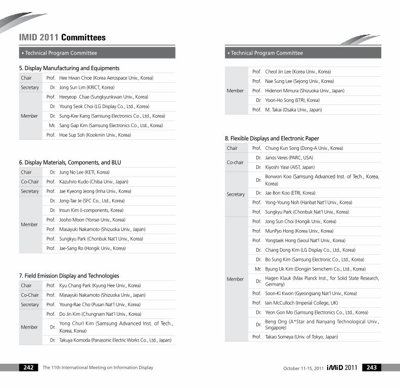
The 11th International Meeting on Information Display242 October 11-15, 2011 243
IMID 2011 Committees
5. Display Manufacturing and Equipments
Chair Prof. Hee Hwan Choe (Korea Aerospace Univ., Korea)
Secretary Dr. Jong Sun Lim (KRICT, Korea)
Member
Prof. Heeyeop Chae (Sungkyunkwan Univ., Korea)
Dr. Young Seok Choi (LG Display Co., Ltd., Korea)
Dr. Sung-Kee Kang (Samsung Electronics Co., Ltd., Korea)
Mr. Sang Gap Kim (Samsung Electronics Co., Ltd., Korea)
Prof. Hoe Sup Soh (Kookmin Univ., Korea)
6. Display Materials, Components, and BLU
Chair Dr. Jung No Lee (KETI, Korea)
Co-Chair Prof. Kazuhiro Kudo (Chiba Univ., Japan)
Secretary Prof. Jae Kyeong Jeong (Inha Univ., Korea)
Member
Dr. Jong-Tae Je (SFC Co., Ltd., Korea)
Dr. Insun Kim (i-components, Korea)
Prof. Jooho Moon (Yonsei Univ., Korea)
Prof. Masayuki Nakamoto (Shizuoka Univ., Japan)
Prof. Sungkyu Park (Chonbuk Nat'l Univ., Korea)
Prof. Jae-Sang Ro (Hongik Univ., Korea)
7. Field Emission Display and Technologies
Chair Prof. Kyu Chang Park (Kyung Hee Univ., Korea)
Co-Chair Prof. Masayuki Nakamoto (Shizuoka Univ., Japan)
Secretary Prof. Young-Rae Cho (Pusan Nat'l Univ., Korea)
Member
Prof. Do Jin Kim (Chungnam Nat'l Univ., Korea)
Dr.Yong Churl Kim (Samsung Advanced Inst. of Tech., Korea, Korea)
Dr. Takuya Komoda (Panasonic Electric Works Co., Ltd., Japan)
Technical Program Committee
Member
Prof. Cheol Jin Lee (Korea Univ., Korea)
Prof. Nae Sung Lee (Sejong Univ., Korea)
Prof. Hidenori Mimura (Shizuoka Univ., Japan)
Dr. Yoon-Ho Song (ETRI, Korea)
Prof. M. Takai (Osaka Univ., Japan)
8. Flexible Displays and Electronic Paper
Chair Prof. Chung Kun Song (Dong-A Univ., Korea)
Co-chairDr. Janos Veres (PARC, USA)
Dr. Kiyoshi Yase (AIST, Japan)
Secretary
Dr.Bonwon Koo (Samsung Advanced Inst. of Tech., Korea, Korea)
Dr. Jae Bon Koo (ETRI, Korea)
Prof. Yong-Young Noh (Hanbat Nat'l Univ., Korea)
Prof. Sungkyu Park (Chonbuk Nat'l Univ., Korea)
Member
Prof. Jong Sun Choi (Hongik Univ., Korea)
Prof. MunPyo Hong (Korea Univ., Korea)
Prof. Yongtaek Hong (Seoul Nat'l Univ., Korea)
Dr. Chang Dong Kim (LG Display Co., Ltd., Korea)
Dr. Bo Sung Kim (Samsung Electronic Co., Ltd., Korea)
Mr. Byung Uk Kim (Dongjin Semichem Co., Ltd., Korea)
Dr.Hagen Klauk (Max Planck Inst., for Solid State Research, Germany)
Prof. Soon-Ki Kwon (Gyeongsang Nat'l Univ., Korea)
Prof. Iain McCulloch (Imperial College, UK)
Dr. Yeon Gon Mo (Samsung Electronics Co., Ltd., Korea)
Dr.Beng Ong (A*Star and Nanyang Technological Univ., Singapore)
Prof. Takao Someya (Univ. of Tokyo, Japan)
Technical Program Committee

The 11th International Meeting on Information Display244 October 11-15, 2011 245
IMID 2011 Committees
9. LC Technologies
Chair Prof. Jong Hyun Kim (Chungnam Nat'l Univ., Korea)
Co-chairProf. Munehiro Kimura (Nagaoka Univ. of Tech., Japan)
Prof. Lachezar Komitov (Univ. of Gothenburg, Sweden)
Secretary Prof. Chang-Jae Yu (Hanyang Univ., Korea)
Member
Prof. Liang-Chy Chien (Kent State Univ., USA)
Prof.Vladimir G. Chigrinov (The Hong Kong Univ. of Science and Tech., Hong Kong)
Prof. Suk-Won Choi (Kyung Hee Univ., Korea)
Prof. Wolfgang Haase (Darmstadt Univ. of Tech., Germany)
Prof. Daeseung Kang (Soongsil Univ., Korea)
Prof. Jae-Hoon Kim (Hanyang Univ., Korea)
Prof. Hak-Rin Kim (Kyungpook Nat'l Univ., Korea)
Prof. Gi-Dong Lee (Dong-A Univ., Korea)
Prof. Myong-Hoon Lee (Chonbuk Nat'l Univ., Korea)
Prof. Seung Hee Lee (Chonbuk Nat'l Univ., Korea)
Dr. Seung-Eun Lee (Merckgroup, Korea)
Prof. Masanori Ozaki (Osaka Univ., Japan)
Dr. Kyunil Rah (LG Chem., Korea)
Prof. Qiong-Hua Wang (Sichuan Univ., China)
Dr.Oleg Yaroshchuk (Nat’l Academy of Sciences of Ukraine Inst. of Physics, Ukraine)
10. LED
Chair Prof. Young Mun Yu (Pukyong Nat'l Univ., Korea)
Member
Dr. Jong Hyeob Baek (KOPTI, Korea)
Dr. Sangsu Hong (Samsung Electro-Mechanics Co.,Ltd., Korea)
Prof. Ja-Soon Jang (Yeungnam Univ., Korea)
Dr. Tae Gyu Kang (ETRI, Korea)
Mr. Won Kuk Son (POSCO LED, Korea)
Technical Program Committee
11. Lighting and Extraction Technologies
Chair Prof. Byoungchoo Park (Kwangwoon Univ., Korea)
Secretary Prof. Sung Min Cho (Sungkyunkwan Univ., Korea)
Member
Dr. Tae Hyun Ban (Kumho Electric, Inc., Korea)
Dr. Mee Ryoung Cho (KILT, Korea)
Dr. Won-gun Jang (KOPTI, Korea)
Prof. Youngkyoo Kim (Kyungpook Nat'l Univ., Korea)
Dr. Mihye Lee (KRICT, Korea)
Prof. S.-T. Lee (City Univ. of Hong Kong, Hong Kong)
Prof. Tae-Woo Lee (Pohang Univ. of Science and Tech., Korea)
Prof. Liang-Sheng Liao (Soochow Univ., China)
Prof. Dong Myung Shin (Hongik Univ., Korea)
12. MEMS and Emerging Technologies
Chair Prof. Jun Bo Yoon (KAIST, Korea)
Member
Prof. Jinnil Choi (Korea Univ., Korea)
Prof. Mi Sook Chung (Korea Polytechnic Univ., Korea)
Prof. Byeong Hee Kim (Kangwon Nat'l Univ., Korea)
Prof. Daekeun Kim (Dankook Univ., Korea)
Prof. Sunghoon Kwon (Seoul Nat'l Univ., Korea)
Prof. Jeong Bong Lee (UT Dallas, USA)
Prof. Wounjhang Park (Colorado Univ., USA)
Prof. Jae-Hyoung Park (Dankook Univ., Korea)
Dr. Hyun Joon Shin (KIST, Korea)
Dr. Nan Ei Yu (GIST, Korea)
Technical Program Committee

The 11th International Meeting on Information Display246 October 11-15, 2011 247
IMID 2011 Committees
13. OLED
Chair Prof. Chang-Hee Lee (Seoul Nat'l Univ., Korea)
Co-chair Dr. Julie Brown (UDC, USA)
Secretary Prof. Min Chul Suh (Kyung Hee Univ., Korea)
Member
Prof. Chihaya Adachi (Kyushu Univ., Japan)
Dr. Jan Blochwitz-Nimoth (NOVALED AG, Germany)
Prof. Do-Hoon Hwang (Pusan Nat'l Univ., Korea)
Prof. Changsoon Kim (Seoul Nat'l Univ., Korea)
Dr. Ji-Seon Kim (Imperial College London, UK)
Prof. Jang Hyuk Kwon (Kyung Hee Univ., Korea)
Prof. Jun Yeob Lee (Dankook Univ., Korea)
Dr. Jeong-Ik Lee (ETRI, Korea)
Dr. Bjorn Lussem (Technische Universitat Dresden, Germany)
Prof. Dae-Gyu Moon (Soonchunhyang Univ., Korea)
Prof. Yongsup Park (Kyung Hee Univ., Korea)
Prof. Franky So (Univ. of Florida, USA)
Prof. Chung-Chih Wu (Nat'l Taiwan Univ., Taiwan)
Dr. Joong Hwan Yang (LG Display Co., Ltd., Korea)
Prof. Seunghyup Yoo (KAIST, Korea)
14. PDP
Chair Prof. Ho-Jun Lee (Pusan Nat'l Univ., Korea)
Co-chair Prof. Hiroshi Kajiyama (Hiroshima Univ., Japan)
Secretary
Prof.Joong Kyun Kim (Seoul Nat'l Univ. of Science and Tech., Korea)
Prof. Jeong-Hyun Seo (Incheon Univ, Korea)
Prof. Bhum Jae Shin (Sejong Univ., Korea)
Technical Program Committee
Member
Prof. Kyung Cheol Choi (KAIST, Korea)
Dr. Woo Joon Chung (Samsung SDI, Korea)
Dr. Yunkwon Jung (LG Electronics Inc., Korea)
Prof. Hae June Lee (Pusan Nat'l Univ., Korea)
Dr. Ryuichi Murai (Panasonic, Japan)
Dr. Hyoungbin Park (Samsung SDI Co.,Ltd., Korea)
Prof. Heung-Sik Tae (Kyungpook Nat'l Univ., Korea)
Prof. Harm Tolner (Tolner Technology, The Netherlands)
Dr.Qun Yan (Changhong COC Display Devices Co. Inc., China)
15. Phosphors
Chair Prof. Kee-Sun Sohn (Sunchon Nat'l Univ., Korea)
Co-chair Dr. Rong-Jun Xie (NIMS, Japan)
Secretary Prof. Ji Sik Kim (Kyungpook Nat'l Univ., Korea)
Member
Prof. Seong-Hyeon Hong (Seoul Nat'l Univ., Korea)
Prof. Won Bin Im (Chonnam Nat'l Univ., Korea)
Prof. Duk Young Jeon (KAIST, Korea)
Prof. Lin Jun (Changchun Inst. of Applied Chemistry, China)
Dr. Ha-Kyun Jung (KRICT, Korea)
Prof. Masato Kakihana (Tohoku Univ., Japan)
Prof. You Hyuk Kim (Dankook Univ., Korea)
Prof. Ru-Shi Liu (Nat'l Taiwan Univ., Taiwan)
Prof. Kenji Toda (Niigata Univ., Japan)
Dr. Chao-Nan Xu (AIST, Japan)
Prof. Heesun Yang (Hongik Univ., Korea)
Dr. Chulsoo Yoon (Samsung LED, Korea)
Technical Program Committee

The 11th International Meeting on Information Display248 October 11-15, 2011 249
IMID 2011 Committees
16. Photovoltaics
Chair Prof. Nam-Gyu Park (Sungkyunkwan Univ., Korea)
Co-chair Prof. Hiroshi Segawa (The Univ. of Tokyo, Japan)
Secretary Prof. Hyun Suk Jung (Kookmin Univ., Korea)
Member
Prof. Yi-Bing Cheng (Monash Univ., Australia)
Prof. Yong Soo Cho (Yonsei Univ., Korea)
Dr. Song yuan Dai (Chinese Academy of Sciences, China)
Prof. Shuzi Hayase (Kyushu Institute of Tech., Japan)
Prof. Seigo Ito (Univ. of Hyogo, Japan)
Prof. Yongseok Jun (UNIST, Korea)
Prof. Do-Heyoung Kim (Chonnam Nat'l Univ., Korea)
Prof. Bumjoon Kim (KAIST, Korea)
Dr. Min Jae Ko (KIST, Korea)
Prof. Qingbo Meng (Chinese Academy of Science, China)
Prof. Jong Hyeok Park (Sungkyunkwan Univ., Korea)
17. Projection and Public Display
Chair Dr. Byeongdae Choi (DGIST, Korea)
Co-chair Dr. Koichi Wani (TAZMO, Japan)
Secretary Dr. Jaewook Jeong (DGIST, Korea)
Member
Prof. Hoon Ju Chung (Kumho Nat’l Inst. of Tech., Korea)
Dr. Yoocharn Jeon (HP, USA)
Dr. Sergey Kargapoltsev (LG TCM, Russia)
Mr. Takeda Keigo (SEIKO EPSON, Japan)
Prof. Igor Kompanets (Lebedev Physical Inst., Moscow, Russia)
Prof. Youngtak Lee (GIST, Korea)
Prof. Seoung-Hwan Park (Catholic Univ. of Daegu, Korea)
Dr. Eitoku Shiba (3M, Singapore)
Dr Jungwoo Kim (Samsung Advanced Inst. of Tech., Korea)
Technical Program Committee
MemberProf. Myungchul Yoon (Dankook Univ., Korea)
Prof. Jae Su Yu (Kyung Hee Univ., Korea)
18. Touch and Input Technologies
Chair Prof. Changsik Yoo (Hanyang Univ., Korea)
Co-chair Dr. Tohru Nishibe (Toshiba Matsushita Display, Japan)
Secretary Prof. Sungkyung Park (Pusan Nat'l Univ., Korea)
MemberProf. Kang-Yoon Lee (Konkuk Univ., Korea)
Prof. Yong Sam Moon (Univ. of Seoul, Korea)
Technical Program Committee
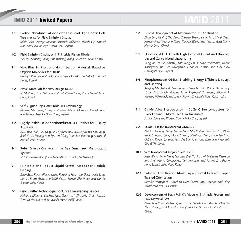
The 11th International Meeting on Information Display250
IMID 2011 Invited Papers
October 11-15, 2011 251
1-1 Carbon Nanotube Cathode with Laser and High Electric Field Treatments for Field Emission Display
Mikio Takai, Tomoya Manabe, Tomoaki Takikawa, Hiroshi Oki, Satoshi Abo, and Fujio Wakaya (Osaka Univ., Japan)
1-2 Field Emission Display with Printable Planar Triode Wei Lei, Xiaobing Zhang, and Baoping Wang (Southeast Univ., China)
2-1 New Blue Emitters and Hole Injection Materials Based on Organic Molecules for OLEDs
Beomjin Kim, Youngil Park, and Jongwook Park (The Catholic Univ. of Korea, Korea)
2-2 Novel Materials for New Design OLED K. M. Fung, S. Y. Ching, and K. W. Cheah (Hong Kong Baptist Univ.,
Hong Kong)
3-1 Self-Aligned Top-Gate Oxide TFT Technology Narihiro Morosawa, Yoshiyuki Oshima, Mitsuo Morooka, Toshiaki Arai,
and Tetsuya Sasaoka (Sony Corp., Japan)
3-2 Highly Stable Oxide Semiconductor TFT Devices for Display Applications
Joon Seok Park, Tae Sang Kim, Kyoung Seok Son, Hyun-Suk Kim, Jong-Baek Seon, Myungkwan Ryu, and Sang Yoon Lee (Samsung Advanced Inst. of Tech., Korea)
4-1 Solar Energy Conversion by Dye Sensitized Mesoscopic Systems
Md. K. Nazeeruddin (Swiss Federal Inst. of Tech., Switzerland)
6-1 Printable and Robust Liquid Crystal Modes for Flexible Displays
Soon-Bum Kwon (Hoseo Univ., Korea), Ji-Hoon Lee (Pusan Nat’l Univ., Korea), Burm-Young Lee (NDIS Corp., Korea), Zhe Hong, and Yan Jin (Hoseo Univ., Korea)
7-1 Field Emitter Technologies for Ultra Fine Imaging Devices Hidenori Mimura, Yoichiro Neo, Toru Aoki (Shizuoka Univ., Japan),
Tomoya Yoshida, and Masayoshi Nagao (AIST, Japan)
7-2 Recent Development of Materials for FED Application Zhuo Sun, Huili Li, Tao Feng, Zhejuan Zhang, Likun Pan, Yiwei Chen,
Xianqin Piao, Xiaohong Chen, Xiaojun Wang, and Ting Lu (East China Normal Univ., China)
8-1 Fluorescent OLEDs with High External Quantum Efficiency beyond Conventional Upper Limit
Yong-Jin Pu, Go Nakata, Jian-Yong Hu, Yusuke Yamashita, Kenta Kobayashi, Daisuke Yokoyama, Hisahiro Sasabe, and Junji Kido (Yamagata Univ., Japan)
8-4 Phosphorescent OLEDs: Enabling Energy Efficient Displays and Lighting
Ruiqing Ma, Peter A. Levermore, Alexey Dyatkin, Zeinab Elshenawy, Vadim Adamovich, Huiqing Pang, Raymond C. Kwong, Michael S. Weaver, Mike Hack, and Julie J. Brown (Universal Display Corp., USA)
9-1 Cu-Mn Alloy Electrodes on In-Ga-Zn-O Semiconductors for Back-Channel-Etched Thin Film Transistors
Junichi Koike and Pil Sang Yun (Tohoku Univ., Japan)
9-2 Oxide TFTs for Transparent AMOLED Chi-Sun Hwang, Sang-Hee Ko Park, Min Ki Ryu, Himchan Oh, Woo-
Seok Cheong, Sung Mook Chung, Shinhyuk Yang, Doo-Hee Cho, OhSang Kwon, Eunsook Park, Jae Eun Pi, In Yong Eom, and Kyeong-Ik Cho (ETRI, Korea)
10-1 Semitransparent Organic Solar Cells Xizu Wang, Ging Meng Ng, Jian Wei Ho (Inst. of Materials Research
and Engineering, Singapore), Tam Hoi Lam, and Furong Zhu (Hong Kong Baptist Univ., Hong Kong)
12-1 Polarizer Free Reverse-Mode Liquid Crystal Gels with Super Twisted Orientation
Rumiko Yamaguchi, Koichiro Goto (Akita Univ., Japan), and Oleg Yaroshchuk (NASU, Ukraine)
12-2 Development of Push-Pull VA Mode with Simple Process and Low Material Cost
Chao Ping Chen, Yanbing Qiao, Lili Liu, Chia-Te Liao, Yu-Wen Chiu, Te-Chen Chung, and Tean-Sen Jen (Infovision Optoelectronics Co. Ltd., China)

The 11th International Meeting on Information Display252
IMID 2011 Invited Papers
October 11-15, 2011 253
13-1 Hafnium Nitride Thin Film Cold Cathode for Field Emitter Arrays
Yasuhito Gotoh and Hiroshi Tsuji (Kyoto Univ., Japan)
13-2 Application of One-Dimensional Nanomaterial Field Emitter in Field Emission Display
Jun Chen, Shaozhi Deng, Ningsheng Xu, Jie Luo, Liyuan Liu, Guofu Zhang, Yanlin Ke, Baohong Li, Yuxiang Chen, Kai Huang, Jian Chen, and Gengxing Liu (Sun Yat-Sen Univ., China)
14-1 Considerations in Designing Efficient Organic Light Emitting Diodes at High Brightness
Z. B. Wang, M. G. Helander, J. Qiu, and Z. H. Lu (Univ. of Toronto, Canada)
14-2 Applications and Physics of Transition Metal Oxides for Organic Light-Emitting Devices
Wolfgang Kowalsk, Sami Hamwi, Katrin Schultheiß, Daniela Donhauser, and Michael Kröger (Technische Universität Braunschweig, Germany)
14-5 Low Power, Red, Green and Blue Carbon Nanotube Enabled Vertical Organic Light Emitting Transistors for Active Matrix OLED Displays
Mitchell A. McCarthy, Bo Liu, Evan P. Donoghue (Univ. of Florida, USA), Ivan Kravchenko (Oak Ridge Nat’l Lab., USA), Do Young Kim, Franky So, and Andrew G. Rinzler (Univ. of Florida, USA)
15-1 Density of Trap States of Measured by Photo-Excited Charge-Collection Spectroscopy into Oxide Thin-Film Transistors
Seongil Im, Youn-Gyoung Chang (Yonsei Univ., Korea), Tae Woong Moon (LG Display Co., Ltd., Korea), Kimoon Lee (Tokyo Inst. of Tech., Japan), and Jae Hoon Kim (Yonsei Univ., Korea)
16-1 Nanocrystalline-TiO2 Electrodes for Dye-Sensitized, Compound (CuInS2) and Extremely-Thin-Absorber (Sb2S3) Solar Cells
Seigo Ito (Univ. of Hyogo, Japan)
16-2 Non-Vacuum Process of Cu-In-Ga-Se/S Thin Film Photovoltaic Cells
Ji-Hyun Cha, Juyeon Chang, Yeji Lee (Sungkyunkwan Univ., Korea), Jong Hyeon Lee (The Catholic Univ. of Korea, Korea), and Duk-Young Jung (Sungkyunkwan Univ., Korea)
17-1 World’s First 70” UD 240Hz LCD TV for 3D Application Bong Hyun You (Seoul Nat’l Univ., Korea), Jae Sung Bae, Dong Won
Park, and Sung Tae Shin (Samsung Electronics Co., Ltd., Korea)
17-2 Switchable and Tunable Liquid Crystal Lens for Autostereo-scopic 3D Displays
Brian Li, Yinwei Chen, and Xiaoda Gong (SuperD Co., Ltd., China)
17-3 Zero-Zero-Birefringence Polymers and Their Applications to LCD
Akihiro Tagaya and Yasuhiro Koike (Keio Univ., Japan)
17-4 Organic Microdisplays for Head-Mounted Display Applications Karsten Fehse, Christian Schmidt, Rigo Herold, Bernd Richter, and Uwe
Vogel (Fraunhofer IPMS, Germany)
18-1 Biaxial Nature of Laterally-Connected Nematic Liquid Crystal Isa Nishiyama (DIC Corp., Japan), Yuka Tabe (Waseda Univ., Japan), Jun
Yamamoto, Yoichi Takanishi, Yoko Ishii (Kyoto Univ., Japan), and Hiroshi Yokoyama (Kent State Univ., USA)
18-2 Microlens Array Based on Electronic Pattering Method Using Electrohydrodynamic Instability
You-Jin Lee, Young Wook Kim, Chang-Jae Yu, and Jae-Hoon Kim (Hanyang Univ., Korea)
19-1 Field Emitter Array Technologies Developed in AIST Masayoshi Nagao and Tomoya Yoshida (AIST, Japan)
19-2 Defect-Related Photoluminescence in Silica, Magnesia, and Alumina
Takashi Uchino (Kobe Univ., Japan)
20-1 Advancements in PIN-OLED Stack Design for AM-OLED Displays Highlighting Inverted OLEDs for Easy N-Channel Backplane Integration
Andreas Haldi, Qiang Huang, Oliver Langguth, Tobias Canzler, and Jan Birnstock (Novaled AG, Germany)
20-2 Enhanced Charge Injection Caused by Molecular Orientation at Organic/Organic Interface
Toshinori Matsushima and Hideyuki Murata (Japan Advanced Inst. of Science and Tech., Japan)
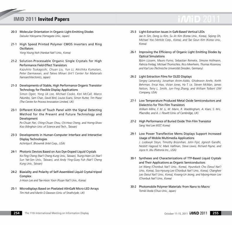
The 11th International Meeting on Information Display254
IMID 2011 Invited Papers
October 11-15, 2011 255
20-3 Molecular Orientation in Organic Light-Emitting Diodes Daisuke Yokoyama (Yamagata Univ., Japan)
21-1 High Speed Printed Polymer CMOS Inverters and Ring Oscillators
Yong-Young Noh (Hanbat Nat’l Univ., Korea)
21-2 Solution-Processable Organic Single Crystals for High Performance Field-Effect Transistors
Kazuhito Tsukagoshi, Chuan Liu, Yun Li, Akichika Kumatani, Peter Darmawan, and Takeo Minari (Int’l Center for Materials Nanoarchitectonics, Japan)
21-3 Developments of Stable, High Performance Organic Transistor Technology for Flexible Display Applications
Simon Ogier, Yong Uk Lee, Michael Cooke, Keri McCall, Marco Palumbo, Sam Chan, David Bird, Louise Evans, Simon Rutter, Tim Pease (The Centre for Process Innovation Limited, UK)
23-1 Different Kinds of Touch Panel with the Signal Detecting Method for the Present and Future Technology and Development
Po-Chuan Pan, Ching-Chuan Chou, Chi-Hwa Cheng, and Horng-Show Koo (Minghsin Univ. of Science and Tech., Taiwan)
23-3 Developments in Human-Computer Interface and Interactive Display Technologies
Achintya K. Bhowmik (Intel Corp., USA)
24-1 Photonic Devices Based on Azo Dye-Doped Liquid Crystals Ko-Ting Cheng (Nat’l Cheng Kung Univ., Taiwan), Tsung-Hsien Lin (Nat’l
Sun Yat-Sen Univ., Taiwan), and Andy Ying-Guey Fuh (Nat’l Cheng Kung Univ., Taiwan)
24-2 Biaxiality and Polarity of Self-Assembled Liquid Crystal-tripod Complex
Ji-Hoon Lee and Tae-Hoon Yoon (Pusan Nat’l Univ., Korea)
25-1 Microdisplays Based on Pixelated AlInGaN Micro-LED Arrays Tim Holt and Martin D Dawson (Univ. of Strathclyde, UK)
25-3 Light-Extraction Issues in GaN-Based Vertical LEDs Jae In Sim, Dong Ju Kim, Su Jin Kim (Korea Univ., Korea), Sejong Oh,
Michael Yoo (Verticle Corp., Korea), and Tae Geun Kim (Korea Univ., Korea)
26-1 Improving the Efficiency of Organic Light Emitting Diodes by Optical Simulations
Björn Lüssem, Mauro Furno, Sebastian Reineke, Simone Hofmann, Patricia Freitag, Michael Thomschke, Rico Meerheim, Thomas Rosenow, and Karl Leo (Technische Universität Dresden, Germany)
26-2 Light Extraction Films for OLED Displays Sergey Lamansky, Jonathan Anim-Addo, Ghidewon Arefe, Keith
Behrman, Encai Hao, Vivian Jones, Ha T. Le, Steven McMan, James Nelson, Terry L. Smith, Jun-Ying Zhang, and William Tolbert (3M Company, USA)
27-1 Low Temperature Produced Metal Oxide Semiconductors and Dielectrics for Thin Film Transistors
William Milne, F. M. Li, M. Mann, R. Waddingham, A. Kiani, S. M-L. Pfaendler, and A. J. Flewitt (Univ. of Cambridge, UK)
27-2 High Performance of Buried Oxide Thin Film Transistor Sang Yeol Lee (KIST, Korea)
29-1 Low Power Transflective Mems Displays Support Increased Usage of Mobile Multimedia Applications
J. Lodewyk Steyn, Timothy Brosnihan, John Fijol, Jignesh Gandhi, Nesbitt Hagood IV, Mark Halfman, Steve Lewis, Richard Payne, and Joyce H. Wu (Pixtronix Inc., USA)
30-1 Syntheses and Characterizations of TTF-Based Liquid Crystals and Their Applications as Organic Semiconductors
Lei Wang (Chonbuk Nat’l Univ., Korea), Hyunduck Cho (Seoul Nat’l Univ., Korea), Soo-Hyoung Lee (Chonbuk Nat’l Univ., Korea), Changhee Lee (Seoul Nat’l Univ., Korea), Kwang-Un Jeong, and Myong-Hoon Lee (Chonbuk Nat’l Univ., Korea)
30-2 Photomobile Polymer Materials: from Nano to Macro Tomiki Ikeda (Chuo Univ., Japan)

The 11th International Meeting on Information Display256
IMID 2011 Invited Papers
October 11-15, 2011 257
32-1 Strong Microcavity Effects in Organic Light-Emitting Diodes Jonghee Lee, Simone Hofmann, Michael Thomschke, Mauro Furno,
Yong Hyun Kim, Björn Lüssem, and Karl Leo (Technische Universität Dresden, Germany)
32-4 Outcoupling Efficiency in ITO and Graphene Based Organic Light Emitting Diodes
Jang-Joo Kim and Sei-Yong Kim (Seoul Nat’l Univ., Korea)
33-1 Downscaling Issues and Drain Filed Relief Architectures in Polysilicon TFTs
G. Fortunato, M. Cuscunà, L. Maiolo, L. Mariucci, M. Rapisarda, A. Pecora, A. Valletta (IMM-CNR, Italy), and S. D. Brotherton (TFT Consultant, UK)
33-2 Wireless-Communication to the Display Panel and TFTs on Heat-Resistant Transparent Film
Mutsuko Hatano (Tokyo Inst. of Tech., Japan) , Takashi Hattori, Futoshi Furuta (Hitachi Ltd., Japan), and Makoto Ohkura (Hitachi Displays Ltd., Japan)
34-1 Comparison of 2D and 3D Vision Gaze with Simultaneous Measurements of Accommodation and Convergence among Young and Middle-Aged Subjects
Masaru Miyao, Tomoki Shiomi, Hiroki Hori, Akira Hasegawa (Nagoya Univ., Japan), Hiroki Takada (Univ. of Fukui, Japan), and Satoshi Hasegawa (Nagoya Bunri Univ., Japan)
35-1 New Phosphate Phosphors for Lighting Application Kenji Toda (Niigata Univ., Japan)
35-2 High Efficiency Phosphor LEDs for Full Spectrum Solid State Lighting Technologies
Partha Dutta, Aloka Khanna, and Adam Gennett (Rensselaer Polytechnic Inst., USA)
36-1 A Transflective Blue-Phase Liquid Crystal Display with Single Cell Gap
Qiong-Hua Wang, Feng Zhou, Jian-Peng Cui, and Di Wu (Sichuan Univ., China)
37-1 Organic Transistors Optimized for Channel Materials and Interfaces
Yu Xia, Damien Boudinet, He Yan, Zhihua Chen, Yan Zheng, Jordan Quinn, and Antonio Facchetti (Polyera Corp., USA)
37-2 Lamination Process and Organic Transparent Electrodes for New Organic Light-Emitting Diode Applications
Wataru Mizutani, Kiyomi Tsukagoshi (AIST, Japan), Kazumi Aoba, Hideki Sakai, Takashi Ohmori, Hayato Hyakutake (Denshi Kako, Co.,Ltd., Japan), and Heeyeop Chae (Sungkyunkwan Univ., Korea)
37-4 Ink-Jet Printing of Active and Passive Layers for Flexible Organic Electronic Devices
A. Wedel, B. Fischer, S. Kreissl, A. Lange, and C. Boeffel (Fraunhofer-Inst. for Applied Polymer Research, Germany)
38-1 White OLEDs for Next Generation Solid State Lighting Takuya Komoda, Nobuhiro Ide, Hiroya Tsuji, Kazuyuki Yamae, Yuko
Matsuhisa, and Varutt Kittichungchit (Panasonic Electric Works Co., Ltd., Japan)
38-2 OLED-Based Safe Lighting Source for Display and Lighting at Night
Jwo-Huei Jou, Shih-Ming Shen (Nat’l Tsing Hua Univ., Taiwan), Szu-Hao Chen, Chien-Chih Chen, and Ching-Chiun Wang (ITRI, Taiwan)
39-1 Next Generation Display Fabricated by Bio Nano Process Yukiharu Uraoka, Yosuke Tojo, Kosuke Ohara, Yasuaki Ishikawa, and
Ichiro Yamashita (Nara Inst. of Science and Tech., Japan)
39-2 Effective Annealing of Si Films as a New LTPS Takashi Noguchi, Jean D. Mugiraneza, Toshiharu Suzuki, Katsuya Shirai,
Tatsuya Okada (Univ. of the Ryukyus, Japan), Hideki Matsushima, Takao Hashimoto, Yoshiaki Ogino, Eiji Sahoto (Hitachi Computer Peripherals Co. Ltd., Japan)
40-1 See-Through Display via Polymer Grating Fabricated on Single Substrate
H. T. Dai and X. W. Sun (Tianjin Univ., China)
41-1 (Oxy) Nitride Phosphors Synthesized by Spark Plasma Sintering Seong-Hyeon Hong, Sung-Woo Choi, Eun-Hee Kang, and Yi-Seul Kim
(Seoul Nat’l Univ., Korea)

The 11th International Meeting on Information Display258
IMID 2011 Invited Papers
October 11-15, 2011 259
41-2 Synthesis of Phosphor Materials Using Ordinary Pressure Ammonia
Tadashi Ishigaki, Shinnosuke Kamei, Kazuyoshi Uematsu, Kenji Toda, and Mineo Sato (Niigata Univ., Japan)
41-3 A Novel Low Temperature Process for Synthesizing Nitride Phosphors
Tomoaki Watanabe, Kazumichi Nonaka (Meiji Univ., Japan), Jinwang Li, and Masahiro Yoshimura (Tokyo Inst. of Tech., Japan)
42-1 Investigation of Interaction between Liquid Crystals and Polyimide Alignment Film
Yukio Hirano (Chisso Petrochemical Corp., Japan)
42-2 Nanoscale Imaging of Anisotropic Material by Optical Nanotomography
Yoonseuk Choi (Hanbat Nat’l Univ., Korea) and Charles Rosenblatt (Case Western Reserve Univ., USA)
43-1 Energy Level Engineering at Flexible Organic/Electrode and Organic/Organic Interfaces
Norbert Koch (Humboldt-Universität zu Berlin, Germany)
43-3 Direct Writing Techniques for the Fabrication of Complemen-tary Organic Field-Effect Transistors
Mario Caironi, Sadir Bucella, Krishna Chaitanya Vishunubhatla (Istituto Italiano di Tecnologia, Italy), Enrico Gili, and Henning Sirringhaus (Cavendish Lab., UK)
43-4 Flexible Universal Plane Technology for Active-Matrix Displays Yu-Yang Chang, Jia-Chong Ho, Glory Chen, Liang-You Jiang, Jing-Yi
Yan, Chun-Wei Su, Chyi-Ming Leu, and Cheng-Chung Lee (ITRI, Taiwan)
44-1 OLEDs for Custom Specific Lighting and Signage Applications M. Toerker, J. Hesse, A. Philipp, M. Jahnel, O. Hild, and Ch. May
(Fraunhofer-IPMS, Germany)
44-4 Advances in Monochrome and Full Color SMOLED-On-Silicon Micro-Displays
Tariq A. Ali, Ilyas I. Khayrullin, and Amalkumar P. Ghosh (eMagin Corp., USA)
45-1 PDP Efficiency Vladimir Nagorny (Plasma Dynamics, USA)
45-2 Improvement of Luminous Efficiency Using New Structure in AC-PDPs
Shunsuke Kawai, Koichi Mizuno, Shinichiro Hori, Tomohiro Murakoso, Eichiro Otani, Kimio Amemiya, and Ryuichi Murai (Panasonic Plasma Display Co., Ltd., Japan)
45-3 Characteristics of High Efficiency PDP with MgO-CaO Cathode Layer
Ki-Woong Whang, Tae-Ho Lee, Hee-Woon Cheong, Min-Soo Yoon, and Sang-Ho Park (Seoul Nat’l Univ., Korea)
46-1 The Effect of Display Luminance, Crosstalk and 3D Display Type on Visual Fatigue and Perceived Display Quality
Hyung-Chul O. Li and Jong-Jin Park (Kwangwoon Univ., Korea)
46-2 The 3-D Vision Training Apparatus in the Form of Diffractive Raster Spectacles
Irina G. Palchikova (Technological Design Inst. of Scientific Instrument Engineering, Russia)
47-1 β-SiAlON:Pr3+: a Thermal Stable Red Oxynitride Phosphor Ru-Shi Liu and Tzu-Chen Liu (Nat’l Taiwan Univ., Taiwan)
47-2 New Efficient Solid-Solution Phosphors: Correlation between Crystal Structure and Optical Properties for Solid-State Lighting
Won Bin Im and Kyoung Hwa Lee (Chonnam Nat’l Univ., Korea)
48-1 Human Factors of Stereoscopic 3D TV under Various Ambient Illuminations
Pei-Li Sun, Tai-Hsiang Tseng, Ting-Yuan Chang (Nat’l Taiwan Univ. of Science and Tech., Taiwan), and Ronnier Luo (Univ. of Leeds, UK)
49-1 Ink-Jet Printed Polymer Transistor Arrays for Flexible Reflective Display
Jiyoul Lee, Joo-Young Kim, Byung Wook Yoo, Do Hwan Kim, Bang-Lin Lee, Jeong-Il Park, Jong Won Chung, JiYoung Jung, Bon-Won Koo, Jung Woo Kim, Byunggun Song, Myung Hoon Jung, Jaeeun Jang, and Yong Wan Jin (Samsung Advanced Inst. of Tech., Korea)

The 11th International Meeting on Information Display260
IMID 2011 Invited Papers
October 11-15, 2011 261
49-4 Development of High Resolution and Low-Temperature Printing Techniques for Flexible TFT Device Fabrication
Toshihide Kamata, Manabu Yoshida, Sei Uemura, and Takehito Kodzasa (AIST, Japan)
50-1 Developing CaxMg1-xO (CMO) Protecting Layer for High Luminous Efficacy PDP
Qun (Frank) Yan, Zhengxiang Lu, Fangli Xing, Xing Zhang, Cuizhen Tang, Liguo Chen, Xinqun Deng (Sichuan Shiji shuanghong Display Device Co. Ltd., China), Bin Li, and Dequan Peng (Sichuan Changhong Electric Co.,Ltd. China)
50-2 Exo-Electrons from MgO Nano-Crystals for AC PDPs Keun-Ho Choi and Yong-Seog Kim (Hongik Univ., Korea)
51-1 Low-Cost Manufacturing Process for OLEDs: Solution Printing Marie O’Regan, Reid Chesterfield, and Jonathan Ziebarth (DuPont
Displays, Inc., Canada)
54-1 Quantification of Display Non-Uniformity by Psychophysical Experiment
Byungseok Min (Samsung Electronics Co., Ltd., Korea)
55-1 Organic Semiconductor Morphology and Mobility Modulated by Dielectric Surface Chemistry
Myung-Han Yoon, Su Jin Sung, Gi-Cheol Son (GIST, Korea), Antonio Facchetti, and Tobin J. Marks (Northwestern Univ., Korea)
56-2 Highly Stable Polymer-TFT Devices for Flexible Displays Shizuo Tokito and Daisuke Kumaki (Yamagata Univ., Japan)
58-1 Three-Dimensional Imaging and Display by Integral Photography
Manuel Martínez-Corral, Héctor Navarro, Genaro Saavedra (Univ. of Valencia, Spain), and Bahram Javidi (Univ. of Connecticut, USA)
59-1 Development of Mechanoluminescence Technology for Diagnosis
Chao-Nan Xu (AIST, Japan)
59-2 Research and Development of Quantum Dots as a Wavelength Converter for White LEDs
Byoung-Hwa Kwon, Hyunki Kim, Youngsun Kim, and Duk Young Jeon (KAIST, Korea)
60-1 Power-Constrained Image Processing Techniques for Emissive and Non-Emissive Displays
Chulwoo Lee, Chul Lee, and Chang-Su Kim (Korea Univ., Korea)
62-1 Solution-Processable and Physicochemically Stable Gate Dielectrics for Organic Field-Effect Transistor Applications
Mi Jang and Hoichang Yang (Inha Univ., Korea)
63-2 Improvement of the Light Extraction Efficiency in the GaN Based LED by Motheye Structure
Motoaki Iwaya, Toshiyuki Kondo, Akihiro Ishihara (Meijo Univ., Japan), Tsukasa Kitano, Koichi Naniwae (ELSEED Corp., Japan), Tetsuya Takeuchi, Satoshi Kamiyama, and Isamu Akasaki (Meijo Univ., Japan)
64-1 Virtual Touched 3D Optical Touch System Yi-Pai Huang, Guo-Zhen Wang, Ming-Ching Ma, Shang-Yu Tung, Shu-
Yi Huang (Nat’l Chiao Tung Univ., Taiwan), Hung-Wei Tseng, Chung-Hong Kuo, and Chun-Huai Li (AU Optronics Corp., Taiwan)
65-1 Computational Design of Eu2+-Doped Phosphors: Relationship between Crystal Structure, Electronic Structure, and Emission Property
Hiroaki Onuma, Ryo Nagumo, Ryuji Miura, Ai Suzuki, Hideyuki Tsuboi, Nozomu Hatakeyama, Hiromitsu Takaba, and Akira Miyamoto (Tohoku Univ., Japan)
65-2 Reducing Tb and Eu Usage in Phosphors Tomoko Akai (AIST, Japan)
65-3 Development of High Photoluminescence Nanostructured ZnO Thin Film Phosphor at Low Temperature
Chaoyang Li, Dapeng Wang, Toshiyuki Kawaharamura, Mamoru Furuta, and Akimitsu Hatta (Kochi Univ. of Tech., Japan)
66-1 High Performance Pico-Projection Module Integrated with RGB LED Array and SVGA LCoS Panel
Yong Tak Lee, Sung Jun Jang (GIST, Korea), and Byung Dae Choi (DGIST, Korea)
66-3 Thermal Analysis and Modeling of Light Emitting Diode Array Structures for Projection Applications
Jae Su Yu and Hee Kwan Lee (Kyung Hee Univ., Korea)

The 11th International Meeting on Information Display262
IMID 2011 Invited Papers
October 11-15, 2011 263
67-1 Inkjet Printing of ITO Transparent Electrodes Dania Alsaid, Margaret Joyce, Erika Rebrosova, Marian Rebros, and
Massood Atashbar (Western Michigan Univ., USA)
67-2 High Resolution Electrohydrodynamic Inkjet Printing for Electronics
Jang-Ung Park (Ulsan Nat’l Inst. of Science and Tech., Korea)
68-1 High Efficiency Plasmonic Color Filters for Display Applications Ting Xu, Alex F. Kaplan, Yi-Kuei Wu, and L. Jay Guo (The Univ. of
Michigan, USA)
69-1 Enhanced Light out-Coupling in OLEDs with Microlens Arrays Jin-Peng Yang, Qin-Ye Bao, Yan-Qing Li, Shuit-Tong Lee, and Jian-Xin
Tang (Soochow Univ., China)
71-1 Nanocomposite Scintillator Development and Potential Applications
Brent K. Wagner and Zhitao Kang (Georgia Inst. of Tech., USA)
71-2 Fabrication of Transparent Panels of Plasma Display Using Hydrothermally Synthesized Green, Red, Blue Nanophosphors
Woo-Seuk Song, Ki-Heon Lee, and Heesun Yang (Hongik Univ., Korea)
Awards of Minister of Education, Science and Technology Fabrication of Lateral and Stacked Color Patterns by
Selective Wettability for Display Applications Jong-Ho Hong, Jun-Hee Na, Hongmei Li, and Sin-Doo Lee (Seoul
Nat’l Univ., Korea)
Merck Grand Awards 15-2 Drain Bias Induced Instability Characteristics in Oxide Thin
Film Transistors Shinhyuk Yang, Jun Yong Bak (ETRI, Korea), Sung-Min Yoon (Kyung
Hee Univ., Korea), Min Ki Ryu, Himchan Oh, Chi-Sun Hwang, Sang-Hee Ko Park (ETRI, Korea), and Jin Jang (Kyung Hee Univ., Korea)
············································································································ p 47
24-4 Direct Switching Between Planar and Focal Conic States of a Bistable Dual Frequency Cholesteric Liquid Crystal Light Shutter
Pankaj Kumar, Suck Jae Shin, Myong-Hoon Lee, Seung Hee Lee, and Shin-Woong Kang (Chonbuk Nat’l Univ., Korea)
············································································································ p 67
53-2 Synthes i s of the High Luminescence Yel low (Sr,Ba)2SiO4:Eu2+ Phosphor Using a Novel Water Soluble Silicon Compound
Satoko Tezuka, Hideki Kato (Tohoku Univ., Japan), Yuji Takatuka (Sumitomo Metal Mining Co., Ltd., Japan), and Masato Kakihana (Tohoku Univ., Japan)
·········································································································· p 162
Merck Young Scientists Awards 22-1 Effect of the Active Layer Thickness on the Short-Circuit
Current Analyzed by the Generalized Transfer Matrix Method
Sungyeop Jung (Kyunghee Univ., Korea), Yeon-Il Lee, Jun-Ho Youn, Hie-Tae Moon (KAIST, Korea), Jin Jang, and Jungho Kim (Kyunghee Univ., Korea)
············································································································ p 63
62-3 Color Tunable Surface Using Superparamagnetic Nanocomposite Material
Jiyun Kim, Howon Lee, and Sunghoon Kwon (Seoul Nat’l Univ., Korea)
·········································································································· p 181
IMID 2011 Awarded Papers

The 11th International Meeting on Information Display264 October 11-15, 2011 265
IMID 2011 Awarded Papers IMID 2011 Awarded Papers
KIDS Awards (Sponsored by Samsung Electronics) Gold 42-4 Pretilt Angle Control from Homogeneous to Homeotropic
Using Photocurable Monomer Jeong-Hun Lee (Soongsil Univ., Korea), Hyo Kang (Samsung Advanced
Inst. of Tech., Korea), Jin Seol Park, and Daeseung Kang (Soongsil Univ., Korea)
········································································································· p 101
Silver 15-4 Zirconium-Zinc-Tin Oxide Thin-Film Transistors Using a
Solution Process You Seung Rim, Dong Lim Kim, Woong Hee Jeong, Hyun Soo Lim,
and Hyun Jae Kim (Yonsei Univ., Korea) ………………………………………………………………………… p 48
KIDS Awards (Sponsored by LG Display) Gold 20-5 Universal Low Optimum Doping Concentration in
PHOLEDs by Managing Charge Transport Materials Chang Woo Seo and Jun Yeob Lee (Dankook Univ., Korea)
………………………………………………………………………… p 59
Silver 63-3 Highly Efficient, Phosphorescent White Organic Light-
Emitting Diodes (WOLEDs) Fabricated by Solution Processes
Mi-Ri Choi, Tae-Hee Han (POSTECH, Korea), Dae Hwan Oh, Yun-Hi Kim (Gyeongsang Nat’l Univ., Korea), Soon-Ki Kwon (Gyeongsang Nat’l Univ., Korea), and Tae-Woo Lee (POSTECH, Korea)
………………………………………………………………………… p 183
Outstanding Poster Paper Award P1-7 Stability of Solution-Processed LaInZnO Thin-Film Transistors Si Joon Kim, Doo Na Kim, Dong Lim Kim, Doo Hyun Yoon, and Hyun
Jae Kim (Yonsei Univ., Korea) ·········································································································· p 115
P1-54 Wide-Viewing Vertically-Aligned Liquid Crystal Displays with Surface Microstructure Formation Using Colloidal Particles
Seung Chul Park, Jun-Hee Na, and Sin-Doo Lee (Seoul Nat’l Univ., Korea)
·········································································································· p 137
P1-68 Thermal Stability of Blue Phase I Doped with Bent-Core Molecules
Sung-Taek Hur and Suk-Won Choi (Kyung Hee Univ., Korea) p 143
P1-82 Metal Oxide Nanoparticles as an Electron Extraction Layer for Inverted Polymer Solar Cells
Seunguk Noh, Jun Young Kim, Donggu Lee, and Changhee Lee (Seoul Nat’l Univ., Korea)
·········································································································· p 148
P2-4 Techniques to Enhance the Sense of Depth Using Visual Perception Characteristics
Ji Young Hong, Ho Young Lee, Du Sik Park, and Chang Yeong Kim (Samsung Advanced Inst. of Tech., Korea)
·········································································································· p 204
P2-21 Fabrication of Nano-Scale and Large-Area Single-Crystal Silicon Structures by the Printing Method
Jung Ho Park (Korea Univ., Korea), Jung-Hun Seo (Univ. of Wisconsin-Madison, USA), Tae-Yeon Oh, Seongpil Chang (Korea Univ., Korea), Zhenqiang Ma (Univ. of Wisconsin-Madison, USA), and Byeong-Kwon Ju (Korea Univ., Korea)
·········································································································· p 211
P2-43 Surface-Mediated Inkjet Printing Process and Its Application for High Resolution Thin Film Transistor
Dai Geon Yoon and Byung Doo Chin (Dankook Univ., Korea) ·········································································································· p 219
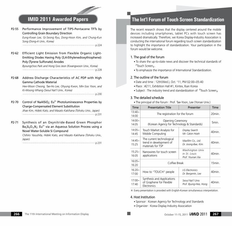
The 11th International Meeting on Information Display266 October 11-15, 2011 267
IMID 2011 Awarded Papers
The recent research shows that the display centered around the mobile devices including smartphones, tablet PCs with touch screen has increased dramatically. Therefore, we Korea Display-Industry Association is conducting the international forum regarding touch screen standardization to highlight the importance of standardization. Your participation in the forum would be welcome.
1. The goal of the forum To share the up-to-state news and discover the technical standards of
『Touch Screen』. To emphasize the importance of International Standardization.
2. The outline of the forum Date and time : 12th(Wed.), Oct. ‘11, PM 02:00~05:40 Place : #211, Exhibition Hall #1, Kintex, Ilsan Korea Subject : The industry trend and standardization of『Touch Screen』
3. The detailed schedule The principal of the forum : Prof. Tae-Yoon, Lee (Yonsei Univ.)
Time Presentation Title Presenter Time13:40~14:00
The registration for the forum 20min.
14:00~14:05
Opening Ceremony(Korean Agency for Technology & Standards) 5min.
14:05~14:45
Touch Market Analysis for Mobile Computing
Display SearchMr. Calvin Hsieh
40min.
14:45~15:25
The current technological trend in development of materials for TSP
Maxfilm Co., Ltd.Dr. Joong-Bae, Kim
40min.
15:25~16:05
Nanowires for touch screen applications
Washington Univ. in St. LouisProf. Younan Xia
40min.
16:05~16:20
Coffee Break 15min.
16:20~17:00
How to “TOUCH” peopleLG ElectronicsDr. Benjamin, Lee
40min.
17:00~17:40
Synthesis and Applications of Graphene for Flexible Electronics
Seoul Nat'l Univ.Prof. Byung-Hee, Hong
40min.
※ Every presentation is provided with English-Korean simultaneous interpretation.
4. Host Institution Sponsor : Korean Agency for Technology and Standards Organizer : Korea Display Industry Association
The Int’l Forum of Touch Screen Standardization
P2-55 Performance Improvement of TIPS-Pentacene TFTs by Controlling Grain Boundary Direction
Eung-Kwan Lee, Gi-Seong Ryu, Dong-Hoon Kim, and Chung-Kun Song (Dong-A Univ., Korea)
·········································································································· p 224
P2-62 Efficient Light Emission from Flexible Organic Light-Emitting Diodes Having Poly (3,4-Ethylenedioxythiophene): Poly (Tyrene Sulfonate) Anodes
Byoungchoo Park and Hong Goo Jeon (Kwangwoon Univ., Korea) ·········································································································· p 228
P2-68 Address Discharge Characteristics of AC PDP with High Gamma Cathode Material
Hee-Woon Cheong, Tae-Ho Lee, Ohyung Kwon, Min-Soo Yoon, and Ki-Woong Whang (Seoul Nat’l Univ., Korea)
·········································································································· p 230
P2-70 Control of NaAlSiO4: Eu2+ Photoluminescence Properties by Charge-Compensated Element Substitution
Jihae Kim, Hideki Kato, and Masato Kakihana (Tohoku Univ., Japan) ·········································································································· p 231
P2-71 Synthesis of an Oxynitride-Based Green Phosphor Ba3Si6O12N2: Eu2+ via an Aqueous Solution Process using a Novel Water-Soluble Si Compound
Chihiro Yasushita, Hideki Kato, and Masato Kakihana (Tohoku Univ., Japan)
·········································································································· p 231

The 11th International Meeting on Information Display268 October 11-15, 2011 269
IMID 2011 ExhibitorsBooth No. Company
1007 OSUNG LST CO., LTD.1009 Display Sector Counsil1010 Canon Semiconductor Engineering Korea Inc.1015 SUNGDO ENG1015 STI1023 Chisso Korea. Co., Ltd1029 LIG ADP Co,. Ltd.1035 LG Display2001 New Gen Tech2001 SP Technology Co., Ltd2002 MAXFILM Corporation2002 Electronic Display Industrial Research Association & Korea2006 Radiant Solution2008 Sanayi System Co., Ltd.2009 Jung Won Corporation2010 TOYO Corporation2012 FINETECH JAPAN / FilmTech JAPAN2014 DISPLAY TAIWAN 20122016 SEPOONG2017 NANOTEK,INC2018 GJM2019 Nikkei Business Publications, Inc.2020 Korea Display Industry Association2021 Shenihen Flat Panel Display Industry Association2023 DAOUXILICON2024 DAEIL SYSTEMS CO.,LTD2025 WOOJOO HI-TECH2026 SUKWON CO.,Ltd.2029 Terasemicon Corporation2033 Wizoptics2034 YTS CO.,LTD2038 sewooincorporation2039 VBKOREA (KURABO)2041 UNILAM Co.,Ltd2042 i-components2045 Metariver Technology Co., Ltd.2046 SUNIC SYSTEM, LTD2047 Mcsicence Inc.2050 Semisysco Co., Ltd.2051 ATS Engineering Co.,Ltd.2054 SNU Precision Co.,Ltd.2058 Toray Engineering Co.,Ltd/TEK Korea Co.,Ltd2059 ISELTEK Co.,Ltd.2064 DAEJOO ELECTRONIC MATERIALS CO.,LTD2066 Merck Advanced Technologies Ltd.3001 LeCroy Korea3002 NAPSON KOREA
Eminent leaders from industries, schools and institutes will give presentations
[Name] : Mr. Calvin Hsieh[Academic background] : M.D. Nat’l Chiao-Tung Univ. (Taiwan)[Company] : Display Search Taiwan[Presentation title] : Touch Market Analys i s for Mobi le
Computing
[Presentation Summary]Hsieh will give a whole picture on touch industry, applications and market status as well as the future trends and critical happening issues with 4 sections.
[Name] : Dr. Joong-Bae, Kim[Academic background] : Ph.D. Bielefeld Univ. (Germany)[Company] : Maxfilm Corporation[Presentation title] : The current technological trend in
development of materials for TSP
[Presentation Summary]The characteristics and technological trends of ITO films and base films, which are widely used as TCOs, will be presented as well as the problems in realization of Narrow Bezel-based technologies.
[Name] : Prof. Younan Xia[Academic background] : Ph.D. Harvard Univ. (US)[Company] : Washington Univ. in St. Louis[Presentation title] : Nanowires for touch screen applications
[Presentation Summary]The presentation will be focused on the experimental issues related to the chemical synthesis of metallic nanowires via solution-phase methods as well as evaluating the potential of current methods and examining the feasibility of new methods.
[Name] : Dr. Benjamin Lee[Academic background] : Ph.D. Seoul Nat’l Univ. (Korea)[Company] : LG Electronics[Presentation title] : How to “Touch” people
[Presentation Summary]Although “Touch” is one of the main features for mobile electronic devices such as smartphones and tablets, it is not a simple story to make touch-enabled devices users satisfied. The presentation will be focused on how to make the users satisfied.
[Name] : Prof. Byung-Hee, Hong[Academic background] : Ph.D. POSTECH (Korea)[Company] : Seoul Nat’l Univ.[Presentation title] : Synthesis & applications of Graphene for
Flexible Electronics
[Presentation Summary]The recent advances in graphene synthesis and applications will be presented together with the future directions of graphene research and development.
The Int’l Forum of Touch Screen Standardization
The 11th International Meeting on Information Display270 October 11-15, 2011 271
AAbo, Satoshi 1-1Adachi, Chihaya 8-2Adamovich, Vadim 8-4Ageno, Scott 61-3Ahn, Byung Du P1-2Ahn, Hyun-A 5-1Ahn, Joo-Seob P1-4Ahn, Seungkwon Keynote ⅠAhn, Sung Il 55-2Ahn, Sung Il P1-41Ahn, Taek P1-77Ahn, Taek P2-85Akai, Tomoko 65-2Akasaki, Isamu 63-2Ali, TariqA. 44-4Alsaid, Dania 67-1Amemiya, Kimio 45-2An, Ho Myoung P1-49An, Hyun Chul P1-30Andou, Takumi 68-2Anim-Addo, Jonathan 26-2Aoba, Kazumi 37-2Aoki, Toru 7-1Arai, Toshiaki 3-1Arefe, Ghidewon 26-2Ashall, Daniel T. 51-4Atashbar, Massood 67-1Avis, Christophe P2-37
BBae, B. S. 23-5Bae, Byung Seong P2-81Bae, Byungseong P2-58Bae, Hyo won P2-66Bae, Hyo won P2-67Bae, Jae Sung 17-1Bae, Jin-Ju P1-80Bae, Jong-Uk 21-4Bae, Jong-Uk 27-3Bae, Jong-Uk 3-3Bae, Jong-Uk 33-3Bae, JongUk P1-14Bae, Jong-Uk P2-27Bae, Jung-Mok 58-3Bae, Kwang-Soo 61-1Bae, Kwang-Soo P1-62Bae, Woo Mi 13-3
Bae, Woo Mi P1-38Bae, Yun-Ju P2-35Baeg, Kang-Jun 49-2Baek, Chang-Hwan 54-4Baek, Ji Hye P2-1Baek, Jong Hyeob P1-42Baek, Jong Hyeob P1-46Baek, Jong Hyeob P1-47Baek, S. H. 23-5Bahlke, Matthias E. 51-4Baik, Kwang Hyeon P1-50Bak, Jun Yong 15-2Bak, Jun Yong P1-10Balaguer, Eva Salvador 70-5Baldo, Marc A. 51-4Bang, Hyung-seok 40-4Bao, Qin-Ye 69-1Baumgarten, Judith 23-4Beccard, Birgit 44-2Beck, Patricia 37-3Behrman, Keith 26-2Bhattacharyya, Surjya Sarathi P2-79Bhowmik, Achintya K. 23-3Bignon, Thibault 34-2Bignon, Thibault 34-3Bird, David 21-3Birnstock, Jan 20-1Blanc, Pierre 34-2Boeffel, C. 37-4Boher, Pierre 34-2Boher, Pierre 34-3Bonucci, Antonio 62-2Boudinet, Damien 37-1Braymen, Steve 67-4Brosnihan, Timothy 29-1Brotherton, S. D. 33-1Brown, Julie J. 8-4Brug, James 67-4Bu, Lyong Sun P1-29Bucella, Sadir 43-3Bunning, Timothy J. 24-3Byeon, Jin-A 70-1Byun, Gui Sob P1-39Byun, Seok Young 70-4Byun, Seok-Joo 70-4
CCaironi, Mario 43-3Canzler, Tobias 20-1
Author IndexIMID 2011 ExhibitorsBooth No. Company
3006 HyBus Co., Ltd.3007 BRUSHBANK3008 CLEAN SYSTEMS KOREA.Inc3010 Ube Material Industries, Ltd.3013 TOPCON KOREA CORPORATION3017 VITRON Co., LTD.3018 Delta ES Co., Ltd.3019 mihro.co.kr3020 BEGATECHNOLOGIES3022 SEKWANG3023 General System Co.3025 DONGA BRUSH3027 OPTICOM CO., LTD3028 ECONY CO.,LTD3031 LMS Corporation3032 ZEON CORPORATION3037 JSR MICRO KOREA3043 SEMYUNG EVER ENERGY CO.,LTD.3045 Rorze Systems Corporation3049 SFA ENGINEERING CORP.3055 Samsung Corning Precision Materials4001 DONGJIN SEMICHEM CO.,LTD.4009 Shinsung FA4041 Wiseplanet Co., Ltd.4045 International Metrology Systems4049 Xyntakem4049 adt Deutschland GmbH4049 AIXTRON Korea Co., Ltd4049 PVA Tepla AG4049 AIXTRON AG4049 Poly IC GmbH & Co.KG4049 FHI fur Photonische Mikrosysteme (IPMS)4049 Fuhrmann Consulting Network4049 Landesmesse Stuttgart GmbH4055 Young Poong CMC Co.,Ltd.4063 Henkel Technologies4065 SHIN Corporation4067 NITTO DENKO4073 TOPTEC Co., Ltd4075 Air Products HYT Inc.4075 Air Products Korea Inc.4081 K-MAC4085 SEHO ROBOT IND.,LTD.4089 SAMSUNG Electronics T.E.S (True Engineering Solution) K.C.Tech SEMES CO.,LTD.
The 11th International Meeting on Information Display272
The 11th International Meeting on Inform
ation Display
October 11-15, 2011 273
Cao, Zhan Feng P1-6Cha, Ji-Hyun 16-2Chae, Hee Yeop P1-30Chae, Heeyeop 37-2Chae, Heeyeop P1-24Chae, Heeyeop P1-25Chae, Heeyeop P1-43Chae, Sung-Min P2-11Chan, Sam 21-3Chandramohan, S. P1-51Chang, Juyeon 16-2Chang, Seongpil P1-18Chang, Seongpil P2-21Chang, Ting-Yuan 48-1Chang, Youn-Gyoung 15-1Chang, Yu-Yang 43-4Cheah, K. W. 2-2Cheah, Kok Wai P1-34Chen, Chao Ping 12-2Chen, Chia-Yu 15-3Chen, Chien-Chih 38-2Chen, Chien-Tao 15-3Chen, Chien-Yue 46-3Chen, Fu-Hao 64-2Chen, Glory 43-2Chen, Glory 43-4Chen, Guohai 7-3Chen, Jian 13-2Chen, Jun 13-2Chen, Kuang-Jung P2-50Chen, Kuan-Ming P1-58Chen, Liguo 50-1Chen, Ni P2-5Chen, Po Hung 11-3Chen, Szu-Hao 38-2Chen, Tian-Yuan P2-59Chen, Tian-Yuan P2-7Chen, Wu-Li 64-2Chen, Xiaohong 7-2Chen, Xu P2-45Chen, Yan-Yu P1-66Chen, Yinwei 17-2Chen, Yiwei 7-2Chen, Yuan-Di 42-3Chen, Yu-Hung 15-3Chen, Yuxiang 13-2Chen, Zhihua 10-2Chen, Zhihua 37-1Cheng, Chi-Hwa 23-1Cheng, Chi-Hwa P2-78
Cheng, Chi-Hwa P2-86Cheng, Horng-Long P1-11Cheng, Hui-Chuan 36-2Cheng, Kai-Chung 15-3Cheng, Ko-Ting 24-1Cheng, Ko-Ting 42-3Cheng, Kung-Yu 43-2Cheong, Hee-Woon 45-3Cheong, Hee-Woon P2-68Cheong, Woo-Seok 9-2Chesterfield, Reid 51-1Chin, Byung Doo 44-3Chin, Byung Doo P2-43Ching, S. Y. 2-2Chiu, Liang-Yun P1-11Chiu, Yu-Wen 12-2Cho, Chuhyun P1-60Cho, Dong Jun P1-65Cho, Doo-Hee 32-2Cho, Doo-Hee 38-3Cho, Doo-Hee 69-2Cho, Doo-Hee 69-3Cho, Doo-Hee 9-2Cho, Hee-Suck P1-85Cho, Hyun Min P1-44Cho, Hyunduck 30-1Cho, Hyunduck P1-17Cho, Hyung Nyuck P1-8Cho, Hyunseok 70-4Cho, Kyeong-Ik 9-2Cho, Kyuman 70-4Cho, Minjun P1-24Cho, Nam Ho 18-3Cho, Sang Hee P1-28Cho, Sung Min P1-29Cho, Sung Min P1-30Cho, Sunghwan P1-24Cho, Yang-ho P2-3Cho, Yang-Ho P2-6Cho, Yong Soo 4-2Cho, Yong Soo 55-3Choi, Byeong Dae 66-2Choi, Byeong-Dae P2-77Choi, Byung Dae 66-1Choi, Byung Gook 3-3Choi, Chung Sock 26-3Choi, Chung Sock 26-4Choi, Heejin 52-4Choi, Heejin 70-1Choi, Hong Kyw 32-2
Author IndexChoi, Hong Rak 55-3Choi, Hyun Chul 52-2Choi, Hyun-Ju P1-37Choi, Ik Jin 4-2Choi, Jin Hwan P1-89Choi, Jin-Hwan P1-37Choi, Jong Sun P2-51Choi, Jong Sun P2-53Choi, Jung Hwan 66-4Choi, Jun-Hyuk 69-4Choi, Keun-Ho 50-2Choi, Ki-Seong P2-56Choi, Kwang Yeol 50-3Choi, Kyu-Hwan 58-3Choi, Kyung Cheol 26-3Choi, Kyung Cheol 26-4Choi, Kyung Cheol 55-2Choi, Kyung Cheol 69-4Choi, Kyung Cheol 71-3Choi, Kyung Cheol P1-89Choi, Kyung Ho P2-49Choi, Kyung Ho P2-52Choi, Kyunghee P2-58Choi, Min Hee 49-3Choi, Mi-Ri 63-3Choi, Seong-Hwan P1-77Choi, Seong-Hwan P2-85Choi, Seongwoo 69-2Choi, Seongwoo 69-3Choi, Seung Chan P1-8Choi, Seung Jin P1-53Choi, SeungChan 3-3Choi, Seung-jin P2-25Choi, Suk-Won 36-4Choi, Suk-Won P1-68Choi, Sungho P2-73Choi, Sungho P2-74Choi, Sungnam P1-90Choi, Sung-Woo 41-1Choi, Sung-Yool 32-2Choi, Sungyoul 19-3Choi, Woo Seok P1-8Choi, Woon-Seop P1-3Choi, Woon-Seop P2-23Choi, Woon-Seop P2-47Choi, Yoonseuk 42-2Choi, Yoon-Sun 58-3Chol, Jinnil P1-39Chou, Ching-Chuan 23-1Chou, Wei-Yang P1-11Chu, Hye Yong 32-2Chu, Hye Yong 38-3Chu, Hye Yong 69-2Chu, Hye Yong 69-3Chuang, Young-Ran 36-2
Chung, Ho Kyun P1-29Chung, Hoon-ju 66-2Chung, Jong Won 49-1Chung, Kwun Bum P1-2Chung, Lung-Pin P2-59Chung, Lung-Yuan P2-78Chung, Lung-Yuan P2-86Chung, Sung Mook 9-2Chung, Te-Chen 12-2Chung, Te-Chen P2-2Chung, Tsung-Ying 34-4Chung, Tsung-Ying 46-3Cooke, Michael 21-3Cremer, Claudia 44-2Cui, Hongqing P2-2Cui, Jian-Peng 36-1Cuscunà, M. 33-1
DDai, H. T. 40-1Darmawan, Peter 21-2Dawson, Martin D. 25-1Deng, Shaozhi 13-2Deng, Xinqun 50-1Diehl, Donald 68-4Dodabalapur, Ananth 21-5Doh, Yoo Jin 14-3Doh, Yoo Jin 8-3Doh, Yoo Jin P1-27Dong, Xin 51-2Donhauser, Daniela 14-2Donoghue, Evan P. 14-5Drees, Martin 10-2Ducin, Izabela P2-76Dutta, Partha 35-2Dyatkin, Alexey 8-4
EElder, Richard 67-4Elshenawy, Zeinab 8-4Eom, In Yong 9-2Eom, Young Ju 13-3Eom, Young Ju P1-38Evans, Louise 21-3Evsevichev, Denis P2-24
FFacchetti, Antonio 10-2Facchetti, Antonio 37-1Facchetti, Antonio 55-1Fan, Kang-Cheng P2-7

The 11th International Meeting on Information Display274
The 11th International Meeting on Inform
ation Display
October 11-15, 2011 275
Fang, Shou-Wei 15-3Feenstra, Johan Keynote ⅢFehse, Karsten 17-4Feng, Tao 7-2Fijol, John 29-1Fischer, B. 37-4Flewitt, A. J. 27-1Fortunato, G. 33-1Freitag, Patricia 26-1Fruehauf, Norbert 5-3Fuh, Andy Ying-Guey 24-1Fuh, Andy Ying-Guey 42-3Fuh, Andy Ying-Guey P1-55Fuh, Andy Ying-Guey P1-66Fujii, Mami P1-84Fujimoto, Kazuhiro P2-82Fujiwara, Isao 68-2Fung, K. M. 2-2Fung, Ka Man P1-34Furno, Mauro 26-1Furno, Mauro 32-1Furuta, Futoshi 33-2Furuta, Mamoru 65-3
GGandhi, Jignesh 29-1Garcia, Robert 67-4Geisow, Adrian 61-3Gennett, Adam 35-2Gersdorff, Markus 44-2Ghosh, Amalkumar P. 44-4Giannantonio, Roberto 62-2Gili, Enrico 43-3Gong, Xiaoda 17-2González, Carlos 70-5Goo, Namhee 52-1Gopi, Baskar 44-2Goto, Koichiro 12-1Gotoh, Yasuhito 13-1Greco, Tonino 59-3Guibourg, Nicolas P2-17Guo, L. Jay 68-1Gupta, Dipti 61-4Gvozdovskyy, Igor P1-72Gwag, Jin Seog P1-71
HHa, An Na 13-3Ha, An Na P1-38Ha, Seunga Kang 54-3Ha, Sung bong P1-86Ha, Sung Bong P1-87
Ha, Tae-Jun 21-5Ha, Yeong-Ho 48-3Ha, Yong-Min 6-3Hack, Mike 8-4Hagood IV, Nesbitt 29-1Hahn, Joonku 58-2Haijun, Qiu P2-14Haldi, Andreas 20-1Halfman, Mark 29-1Hamilton, Sheila 57-1Hamwi, Sami 14-2Han, Chul Jong P1-90Han, Dong Biao 70-1Han, Jeong-In P1-78Han, Jeong-In P2-48Han, Jun-Han 32-2Han, Jun-Han 38-3Han, Jun-Han 69-2Han, Jun-Han 69-3Han, Nam P1-51Han, Tae-Hee 63-3Hao, Encai 26-2Hasegawa, Akira 34-1Hasegawa, Satoshi 34-1Hashimoto, Takao 39-2Hatakeyama, Nozomu 65-1Hatano, Mutsuko 33-2Hatta, Akimitsu 65-3Hattori, Reiji 23-2Hattori, Takashi 33-2Hauschildt, Jason 67-4Helander, M. G. 14-1Helms, Gesa 56-3Henze, Richard 37-3Heo, Jae-Sang P2-40Heo, Ji-Min P2-11Heo, Jun 45-4Heo, Young-Woo P1-15Herold, Rigo 17-4Herrmann, Marcus 5-3Hesse, J. 44-1Heuken, Michael 44-2Hild, O. 44-1Hino, Aya 9-3Hirano, Yukio 42-1Hirata, Takayuki P2-9Ho, Jia-Chong 43-4Ho, Jian Wei 10-1Hofmann, Simone 26-1Hofmann, Simone 32-1Holland, Edward 67-4Holt, Tim 25-1Hong, Chang-Hee 25-2Hong, Chang-Hee P1-51Hong, Chang-Hee P1-52
Hong, Ji Young P2-4Hong, Jisoo 40-2Hong, Jisoo 70-1Hong, Keehoon 70-2Hong, Lin-Ann 2-5Hong, MunPyo 22-2Hong, MunPyo 27-4Hong, MunPyo 67-3Hong, MunPyo P1-13Hong, MunPyo P2-57Hong, MunPyo P2-58Hong, Seong-Hyeon 41-1Hong, Seung Ho 18-3Hong, Seung Ho 36-3Hong, Wan-Shick 57-2Hong, Wan-Shick 57-3Hong, Yongtaek 61-2Hong, Yongtaek 61-4Hong, Zhe 6-1Hong, Zhe P1-85Hongju, Yu P2-14Hori, Hiroki 34-1Hori, Shinichiro 45-2Horita, Masahiro 39-4Horita, Masahiro P1-84Hsieh, Pao-Ju P1-58Hsin, Lung-Pao 15-3Hsu, Heng-Shou 11-3Hsu, Shau-Wei 34-4Hu, Jian-Yong 8-1Huang, Chun-Chieh P2-50Huang, Kai 13-2Huang, Nan Xiong 11-3Huang, Qiang 20-1Huang, Shu-Hao P1-66Huang, Shu-Yi 64-1Huang, Yau-Han P1-55Huang, Yi-Pai 64-1Huh, Jin Woo 32-2Huh, Jin Woo 38-3Huh, Jin Woo 69-2Huh, Jin Woo 69-3Huh, Yoon Ho P2-63Hui, Guan Bao P1-53Hui, Guan Bao P1-6Hur, Seung-Yeol P1-56Hur, Sung-Taek 36-4Hur, Sung-Taek P1-68Hwang , Yong Kee 3-3Hwang, Chi-Sun 15-2Hwang, Chi-Sun 9-2Hwang, Chi-Sun P1-10Hwang, Do-Hoon P1-23Hwang, Gyoung Seok 44-3Hwang, Hye Rim 49-3
Hwang, Joohyun 32-2Hwang, Joohyun 38-3Hwang, Joohyun 69-2Hwang, Joohyun 69-3Hwang, Jung-Won P2-54Hwang, Kyu-young P2-3Hwang, Kyu-Young P2-6Hwang, Sung-Min P1-50Hwang, Wontae P1-24Hwang, Wontae P1-25Hwang, Yong Kee 21-4Hwang, Yong Kee 27-3Hwang, Yong Kee P1-8Hwang, Yong Kee P2-27Hwang, Yong Seok 70-3Hwang, Yong-Kee 29-2Hwang, Yong-Kee 40-4Hwang, YongKee P1-14Hyakutake, Hayato 37-2
IIde, Nobuhiro 38-1Ikeda, Tomiki 30-2Ikenoue, Hiroshi 39-4Im, Chang-Gyu P1-37Im, Dongmo P2-19Im, Hee-Jin 29-2Im, Hee-Jin 40-4Im, Seongil 15-1Im, Won Bin 47-2Ippen, Christian 59-3Ishigaki, Tadashi 41-2Ishiguro, Makoto 68-3Ishihara, Akihiro 63-2Ishii, Yoko 18-1Ishikawa, Yasuaki 39-1Ishikawa, Yasuaki 39-3Ishikawa, Yasuaki 39-4Ishikawa, Yasuaki P1-84Ishinabe, Takahiro 36-2Ito, Seigo 16-1Ito, Yoji 68-2Iwase, Satoshi P2-9Iwaya, Motoaki 63-2
JJackson, Warren 67-4Jahnel, M. 44-1Jam, Mehrban 67-4Jang , Jin 3-4Jang, Chang-Jae 6-3Jang, Cheol 55-2
The 11th International Meeting on Information Display276
The 11th International Meeting on Inform
ation Display
October 11-15, 2011 277
Jang, Il-Soon 31-2Jang, In Kyu P1-42Jang, Jaeeun 49-1Jang, Ja-Soon 31-1Jang, Ji Yun P1-91Jang, Jin Nyoung 22-2Jang, Jin 15-2Jang, Jin 22-1Jang, Jin 49-3Jang, Jing 13-3Jang, Jin P1-38Jang, Jin P2-37Jang, Lee-Woon P1-47Jang, Mi 62-1Jang, Seon-Ho 31-1Jang, Seunghyun 33-5Jang, Sung Jun 66-1Jang, Yong Ho P1-8Jang, YunSung 67-3Jang, YunSung P2-57Javidi, Bahram 58-1Jeans, Albert 67-4Jeffrey, Frank 67-4Jen, T. S. P2-2Jen, Tean-Sen 12-2Jeon, Dae-Woo P1-47Jeon, Duk Young 59-2Jeon, Eun-Young P1-70Jeon, Hong Goo P2-62Jeon, Il P2-46Jeon, Jaeha 72-2Jeon, Ju-Won P1-47Jeon, Myung Jae 50-3Jeon, SangYeop P2-18Jeon, Seong-Ran P1-47Jeon, Taehee 72-2Jeon, Woo Sik 14-3Jeon, Woo Sik 8-3Jeon, Woo Sik P1-27Jeon, Woo Sik P1-83Jeon, Yoocharn 37-3Jeong, Heon 36-3Jeong, Jae Kyeong 9-4Jeong, Jae Kyeong P1-16Jeong, Jaewook 61-2Jeong, Jaewook 66-2Jeong, Jin Doo 31-2Jeong, Jin-Woo 19-3Jeong, Kwang Un P1-61Jeong, Kwang-Un 30-1Jeong, Kwang-Un P1-64Jeong, Kwang-Un P2-79Jeong, Kwnag-Un P2-35Jeong, Kyeong-Min 70-1Jeong, O-Young P1-37
Jeong, Seung Yong P2-49Jeong, Seung Yong P2-52Jeong, Su Seong P2-30Jeong, Won-Ik P1-76Jeong, Won-Ik P1-79Jeong, Woong Hee 15-4Jeong, YeonTaek 27-4Jeong, Youn Hak P1-59Jeong, Young Chul P2-39Ji, Kwang Hwan 9-4Ji, Kwang Hwan P1-16Jian, Ren P2-14Jiang, Liang-You 43-2Jiang, Liang-You 43-4Jin, Haifeng P2-81Jin, Huilian P1-57Jin, Hyun Suk P1-91Jin, Yan 6-1Jin, Yan P1-85Jin, Yong Wan 49-1Jo, Kwang-Min P1-15Jo, Min-Gyeong P1-69Jo, Min-Ji P1-20Jo, Minjun P1-25Jo, Soo In 12-3Jo, Yeon Hwa 4-2Jones, Vivian 26-2Joo, Chul Woong 32-2Joo, Chul Woong 38-3Joo, Chul Woong 69-2Joo, Chul Woong 69-3Joo, Kyung-Il P1-73Jou, Jwo-Huei 38-2Joyce, Margaret 67-1Ju, Byeong Kwon P1-39Ju, Byeong-Kwon 69-2Ju, Byeong-Kwon P1-18Ju, Byeong-Kwon P1-37Ju, Byeong-Kwon P1-89Ju, Byeong-Kwon P2-21Ju, Jin-Woo P1-47Juang, Fuh-Shyang 2-5Jun, Eun P1-30Jun, Myungchul 21-4Jun, Myungchul 27-3Jun, Myungchul 3-3Jun, Myung-Chul 33-3Jun, Myungchul P1-14Jun, Myungchul P1-8Jun, Myungchul P2-27Jung, Duk-Young 16-2Jung, Eun P1-29Jung, Ha-kyun P2-73Jung, Ha-Kyun P2-74Jung, Hong Yoon 9-4
Jung, Hong Yoon P1-16Jung, Jae-Hyun 52-4Jung, Jae-Hyun 58-2Jung, Jae-Hyun 64-4Jung, Jae-Hyun 70-2Jung, JiYoung 49-1Jung, Joohye 16-3Jung, Junghun 46-4Jung, Keum-Dong 33-5Jung, Mee-Suk P2-11Jung, Myung Hoon 49-1Jung, Sang-Duk 5-4Jung, Seung Won P2-22Jung, Sungyeop 22-1Jung, Taeil 63-1Jung, Un-Sung P1-85Jung, Young Jin 63-1Jung, Young-Ho 5-1Junge, Kelly 67-4Junguo, Liu P2-14
KKakarenko, Karol P2-76Kakihana, Masato 53-1Kakihana, Masato 53-2Kakihana, Masato P2-70Kakihana, Masato P2-71Kakihana, Masato P2-72Kamata, Toshihide 49-4Kamei, Shinnosuke 41-2Kamiyama, Satoshi 63-2Kang, Byoung-Ho P1-21Kang, Byoung-Ho P1-80Kang, Chan-mo P1-17Kang, Daeseung 42-4Kang, Dong Han 3-4Kang, Dong-Hoon 48-2Kang, Eun-Hee 41-1Kang, Heon Seok P1-63Kang, Hyo 42-4Kang, Il P1-32Kang, Ji Hye P1-51Kang, Jin-Seong 11-4Kang, Jun-Tae 19-3Kang, S. K. 23-5Kang, Shin Woong P1-64Kang, Shin-Won P1-21Kang, Shin-Won P1-73Kang, Shin-Won P1-80Kang, Shin-Woong 24-4Kang, Shin-Woong P2-79Kang, Sin-Young 57-2Kang, Sin-Young 57-3Kang, So-Hee P1-33
Kang, Tae-gyu 31-2Kang, Taegyu P2-65Kang, Wan Seok 52-2Kang, Wan Seok P1-56Kang, Young Eun P1-62Kang, Zhitao 71-1Kaplan, Alex F. 68-1Kato, Hideki 53-1Kato, Hideki 53-2Kato, Hideki P2-70Kato, Hideki P2-71Kato, Hideki P2-72Kato, Kunihisa P1-19Kawaharamura, Toshiyuki 65-3Kawai, Shunsuke 45-2Ke, Ming-Da 46-3Ke, Yanlin 13-2Keiper, Dietmar 44-2Keum, Chang Min P2-81Keum, Ki-Su 57-2Keum, Ki-Su 57-3Khan, Asad 68-4Khanna, Aloka 35-2Khayrullin, IlyasI. 44-4Ki, Hak Koo P1-89Kiani, A. 27-1Kido, Junji 8-1Kim, Ari 60-2Kim, Beom Jun P2-81Kim, Beomjin 2-1Kim, Beomjin P1-35Kim, Beomjin P1-36Kim, Boram 52-1Kim, BoSung 27-4Kim, Bo-Sung P1-45Kim, Byeong Kon 4-2Kim, Byeong Koo P1-86Kim, Byeong Koo P1-87Kim, Byeong Koo P1-91Kim, Byeong-Koo 52-2Kim, Byeong-Koo 5-4Kim, Byoung Suk P2-17Kim, Byung Soon 49-3Kim, Byunguk P2-58Kim, Chang Dong 33-3Kim, Chang Yeong P2-4Kim, Chang-Dong 21-4Kim, Chang-Dong 27-3Kim, Chang-Dong 3-3Kim, ChangDong P1-14Kim, Chang-Dong P1-8Kim, Chang-Dong P2-27Kim, Chang-Su 60-1Kim, Chi Wan P2-27Kim, Choon-Woo 60-3

The 11th International Meeting on Information Display278
The 11th International Meeting on Inform
ation Display
October 11-15, 2011 279
Kim, Chul Young P1-33Kim, Chung-Gi P1-77Kim, Chung-Gi P2-85Kim, Dae Ho 31-2Kim, Dae Hun 50-3Kim, Dae Hyun P1-59Kim, Dae Hyun P1-61Kim, Dae Hyun P1-86Kim, Dae Hyun P1-87Kim, Dae Kyu P1-86Kim, Dae Kyu P1-87Kim, Dae-Chul 48-3Kim, Dae-Hwan 27-3Kim, Dae-Hwan 3-3Kim, Dae-Kuk P2-80Kim, Dal-Young P2-1Kim, Deok Gi P1-46Kim, Deok-Myeong P2-84Kim, Do Hwan 49-1Kim, Do Young 14-5Kim, Do Young P2-1Kim, Dong Ho P1-48Kim, Dong Ju 25-3Kim, Dong Lim 15-4Kim, Dong Lim 16-3Kim, Dong Lim P1-7Kim, Dong W. 28-2Kim, Dong Wook P2-53Kim, Dong Yoon P1-48Kim, Dong-Hoon P2-55Kim, Dong-Hyun 45-4Kim, Donghyun 61-2Kim, Dong-Hyun P2-69Kim, Dongwook P2-51Kim, DongWoo P1-13Kim, Doo Na P1-7Kim, Doohyun 27-4Kim, Eun Hye P2-39Kim, Eun Kyoung P2-49Kim, Eun Kyoung P2-52Kim, Eun Soo 70-3Kim, Eungtaek 55-2Kim, Ga-Hee 60-3Kim, Gyeong Woo 14-3Kim, Gyeong Woo P1-83Kim, H. J. P2-83Kim, H. K. 23-5Kim, Hak Rin P2-28Kim, Hakkoo P1-37Kim, Hak-Rin 36-4Kim, Hak-Rin P1-73Kim, Hak-Su 5-4Kim, Han-Eol 60-3Kim, Han-Jun 67-4Kim, Han-Pil 70-4
Kim, Han-Pil P2-16Kim, Hee Cheol P1-6Kim, Hee Seop P1-59Kim, Hee Yun P1-51Kim, Hee-Dae P1-77Kim, Hee-Dae P2-85Kim, Hee-Jeong P2-75Kim, Hee-Seung 70-1Kim, Hong-Suk 54-4Kim, Hong-suk 60-2Kim, Hyo Jin P2-39Kim, Hyo Jung 10-3Kim, HyoungJin P1-13Kim, Hyuk Nyun P2-10Kim, Hyuk Nyun P2-22Kim, Hyuk P2-60Kim, Hyuk P2-61Kim, Hyun Jae 15-4Kim, Hyun Jae 16-3Kim, Hyun Jae P1-12Kim, Hyun Jae P1-7Kim, Hyun Jae P1-81Kim, Hyun Kyu P1-51Kim, Hyun-Eui 70-1Kim, Hyung Gu P1-51Kim, Hyunki 59-2Kim, Hyun-Suk 3-2Kim, Insu 31-2Kim, Insu P2-65Kim, Jae Hoon 15-1Kim, Jae Hyun P2-34Kim, Jae Seon P2-54Kim, Jae-Hoon 12-3Kim, Jae-Hoon 18-2Kim, Jae-Hoon 61-1Kim, Jae-Hoon P1-60Kim, Jae-Hoon P1-62Kim, Jae-Ho P2-1Kim, Jaehyun 54-2Kim, Jae-Il P2-16Kim, Jae-Woo 19-3Kim, Jang Ryang P2-10Kim, Jang Ryang P2-22Kim, Jang-Joo 10-3Kim, Jang-Joo 14-4Kim, Jang-Joo 20-4Kim, Jang-Joo 32-3Kim, Jang-Joo 32-4Kim, Jang-Joo 38-4Kim, Jang-Joo P1-76Kim, Jang-Joo P1-79Kim, Jeong Kyu 14-3Kim, Jeong-Joo P1-15Kim, Jeong-kyu P1-83Kim, Ji Ha P1-8
Kim, Ji Whan 10-3Kim, Jigon 63-1Kim, Jihae P2-70Kim, Ji-Hoon P1-23Kim, Ji-Hoon P1-50Kim, Ji-In 9-4Kim, Ji-In P1-16Kim, Jin Yeong 69-4Kim, Jin Yong P2-10Kim, Jin-Chul 31-1Kim, Jisun 11-2Kim, Jiwan P1-90Kim, Jiyoon P2-32Kim, Jiyun 62-3Kim, Jongbin 5-2Kim, Jonghyun 58-2Kim, Jonghyun 70-2Kim, Jong-Hyun P1-74Kim, Jongil 70-4Kim, Jong-Il P2-16Kim, Jong-Man 5-2Kim, JoonDong 11-2Kim, Joo-Young 49-1Kim, Jun Young P1-82Kim, Jung Woo 49-1Kim, Junghan P2-27Kim, Jungho 22-1Kim, Jung-Hye P2-77Kim, Junhoi P2-44Kim, Ki-Han 6-4Kim, Ki-Han P1-57Kim, Ki-Han P1-70Kim, Ki-tae 33-3Kim, Ki-yong P2-25Kim, Kukjoo 55-2Kim, Kwan 6-3Kim, Kwang-Ho P2-40Kim, Kwang-Joon 5-2Kim, Kyeong Hyeon P1-59Kim, Kyu-Jin P1-80Kim, Kyung Min P2-27Kim, Min Chang 70-3Kim, Minsoo 61-2Kim, Min-Sun P1-44Kim, Moon-Seok P2-60Kim, Moon-Seok P2-61Kim, Myoung P1-47Kim, Nam 70-1Kim, Ran P1-32Kim, Sang Mook P1-42Kim, Sang-Ho 6-3Kim, Sang-kee P2-25Kim, SangYoul 51-3Kim, Sei-Min 31-1Kim, Sei-Yong 32-3
Kim, Sei-Yong 32-4Kim, Sei-Yong P1-76Kim, Seok Won P2-39Kim, Seung-Ryul 5-2Kim, Se-Yun P1-15Kim, Si Joon P1-12Kim, Si Joon P1-7Kim, Su Jin 25-3Kim, Su Jin P1-48Kim, Sul Ong P1-31Kim, Sung Hoon 49-3Kim, Sung Ki 33-3Kim, Sung Min P1-52Kim, Sung-Ho 5-4Kim, Sung-Kyu 58-4Kim, Sung-Kyu 72-1Kim, Tae Geun 25-3Kim, Tae Geun P1-48Kim, Tae Geun P1-49Kim, Tae Hyun P2-34Kim, Tae Sang 3-2Kim, Taegeun 40-3Kim, Tae-Min 10-3Kim, Tae-Min 12-3Kim, Tae-Min P1-79Kim, Wan Kyu P1-41Kim, Won Rae P2-10Kim, Woong Sun P2-33Kim, Yeon Gou P2-37Kim, Yi-Seul 41-1Kim, Yong Hyun 32-1Kim, Yong-Hoon P1-5Kim, Yong-Hoon P1-78Kim, Yong-Hoon P2-40Kim, Yong-Hoon P2-48Kim, Yong-Hun 36-4Kim, Yong-Hun P2-28Kim, Yong-Seog 50-2Kim, You Seok 40-3Kim, Youjin 31-2Kim, Youn Jin 54-3Kim, Young Baek P2-63Kim, Young Jin P1-42Kim, Young Kuk P1-63Kim, Young Kwan P1-22Kim, Young Min 46-4Kim, Young Wook 18-2Kim, YoungMin 27-4Kim, Youngmin 64-4Kim, Young-Seok P2-80Kim, Youngsun 59-2Kim, Youngwoo P1-75Kim, Young-Woo P2-36Kim, Younjin 54-2Kim, YounKyung 11-2
The 11th International Meeting on Information Display280
The 11th International Meeting on Inform
ation Display
October 11-15, 2011 281
Kim, YounKyung 72-2Kim, Yun-Gi 45-4Kim, Yun-Hi 63-3Kim, Yun-Hi P1-31Kim, Yun-Hi P1-32Kim, Yun-Hi P1-33Kim, Yun-Jae 52-1Kim, Yun-Joo P2-1Kimball, Brian R. 24-3Kitano, Tsukasa 63-2Kitson, Stephen 61-3Kittichungchit, Varutt 38-1Ko, Jae-Hyeon P2-30Ko, Jae-Hyeon P2-31Ko, Jae-Hyeon P2-34Ko, Jeong Hoon P1-91Ko, Jieun 55-4Ko, Kang-Bok P1-51Ko, Shih-Wei P1-55Ko, Shih-Wei P1-66Kobayashi, Kenta 8-1Koch, Norbert 43-1Kodama, Yuuki P1-88Kodzasa, Takehito 49-4Koh, Jai-wan P2-25Koike, Junichi 9-1Koike, Yasuhiro 17-3Kolodziejczyk, Andrzej P2-76Komoda, Takuya 38-1Kondo, Takeshi P1-19Kondo, Toshiyuki 63-2Koo, Bonseok 54-2Koo, Bon-Won 49-1Koo, Horng-Show 23-1Koo, Horng-Show P2-78Koo, Horng-Show P2-86Koo, HyungJoon P2-46Koo, Min-Sik P1-77Koo, Min-Sik P2-85Kowalsk, Wolfgang 14-2Kravchenko, Ivan 14-5Kreis, Juergen 44-2Kreissl, S. 37-4Kröger, Michael 14-2Ku, Sung-Yu 8-2Kudo, Kazuhiro 56-4Kugimiya, Toshihiro 9-3Kulshreshtha, Chandramouli P1-83Kumaki, Daisuke 56-2Kumar, Pankaj 24-4Kumatani, Akichika 21-2Kunat, Martin 44-2Kunida, Yoshiki P2-9Kuo, Cheng-Ching P2-86Kuo, Chung-Hong 64-1
Kwack, Young Jin P2-23Kwack, Young-Jin P1-3Kwack, Young-Jin P2-47Kwak, Min-Gi P2-80Kwak, Seong Kwon P1-45Kwak, Youngshin 54-2Kwon, Byoung-Hwa 59-2Kwon, Dae-Hyuk P1-21Kwon, Ho Joong 49-3Kwon, Hyunkyung 52-4Kwon, Jae Wook 66-4Kwon, Jang Hyuk 14-3Kwon, Jang Hyuk 8-3Kwon, Jang Hyuk P1-27Kwon, Jang Hyuk P1-83Kwon, Ji-Hye P1-4Kwon, Jin Hyuk P1-71Kwon, Oh-Kyong 11-4Kwon, Oh-Kyong 5-1Kwon, OhSang 9-2Kwon, Ohseung 67-4Kwon, Ohyung P2-60Kwon, Ohyung P2-61Kwon, Ohyung P2-64Kwon, Ohyung P2-68Kwon, So Young P2-49Kwon, So Young P2-52Kwon, Soon-Bum 6-1Kwon, Soon-Bum P1-85Kwon, Soon-Ki 63-3Kwon, Soon-Ki P1-31Kwon, Soon-Ki P1-32Kwon, Soon-Ki P1-33Kwon, Sunghoon 62-3Kwon, Sunghoon P2-44Kwon, Tae-Woo P1-77Kwon, Tae-Woo P2-85Kwon, Yong-Moo 72-1Kwong, Raymond C. 8-4Kyoung, Kyuwon 23-2Kyu, Lee Seong P2-14
LLa, Young Min P1-5Lagerwall, Jan 55-4Lai, Chang-Jun 2-5Lai, Kuang-Chih 2-5Lai, Yu-Cheng P1-58Lai, Yueh-Yi 34-4Lai, Yueh-Yi 46-3Lam, Tam Hoi 10-1Lamansky, Sergey 26-2Lan, Linfeng P1-1Lange, A. 37-4
Langguth, Oliver 20-1Larson, Don 67-4Le, Ha T. 26-2Lee, Bang-Lin 49-1Lee, Bonju 22-2Lee, Burm-Young 6-1Lee, Byoungho 40-2Lee, Byoungho 52-4Lee, Byoungho 58-2Lee, Byoungho 64-4Lee, Byoungho 70-1Lee, Byoungho 70-2Lee, Byoungho P2-5Lee, Byoung-Jun 52-1Lee, Chang-Chun P2-50Lee, Changhee 30-1Lee, Changhee 61-4Lee, Changhee P1-17Lee, Changhee P1-82Lee, Cheng-Chung 43-2Lee, Cheng-Chung 43-4Lee, Cheol Jin 7-3Lee, Cheol Jin P1-40Lee, Choong Ho P2-52Lee, Chul Kwon P1-8Lee, Chul 60-1Lee, Chulwoo 60-1Lee, Do Hyung P2-53Lee, Dong Hyeok 22-2Lee, Dong Wook P1-45Lee, Donggu P1-82Lee, Dong-Hun P1-77Lee, Dong-Hun P2-85Lee, Eun Hye 13-3Lee, Eun Hye P1-38Lee, Eun Ji P1-45Lee, Eung-Kwan P2-55Lee, Gi-Dong 52-2Lee, Gi-Dong P1-56Lee, Guen-Sik 29-2Lee, Guen-Sik 40-4Lee, Gwang Jun 66-2Lee, Gwang-Jun P2-77Lee, Hae June 45-4Lee, Hae June P2-66Lee, Hae June P2-67Lee, Hae June P2-69Lee, Hak Soo P1-30Lee, Hee Kwan 66-3Lee, Ho Jun P2-28Lee, Ho Young P2-4Lee, Ho-Dong 28-2Lee, Ho-Jun 45-4Lee, Ho-Jun P2-66Lee, Ho-Jun P2-67
Lee, Ho-Jun P2-69Lee, Hong-Seok 58-3Lee, Howon 62-3Lee, Ho-young P2-3Lee, Ho-Young P2-6Lee, Hyeok Jin 36-3Lee, Hyuck Jin 18-3Lee, Hyun Hwi 10-3Lee, Hyun Jun P1-89Lee, Hyung Jin P1-26Lee, Hyung Joo P1-42Lee, Hyun-Jun P1-37Lee, Hyun-Ki 31-1Lee, In-Hwan P1-47Lee, Jaeho 33-5Lee, Jaehong 33-5Lee, Jae-Hyun 32-3Lee, Jaejoon 28-1Lee, Jaewon 63-1Lee, Jangkyo 70-4Lee, Je-Hun P1-2Lee, Jen-Yu 15-3Lee, Jeong Yeol P1-6Lee, Jeong-Hun 42-4Lee, Jeong-Hwan 14-4Lee, Jeong-Hwan 20-4Lee, Jeong-Hwan 32-3Lee, Jeong-Ik 32-2Lee, Jeong-Ik 38-3Lee, Jeong-Ik 69-2Lee, Jeong-Ik 69-3Lee, Ji-Hoon 24-2Lee, Ji-Hoon 6-1Lee, Ji-Hoon P1-69Lee, Jiyoul 49-1Lee, Jong Hyeon 16-2Lee, Jong Min P1-26Lee, Jonghee 32-1Lee, Jonghee P1-23Lee, Jongmo P2-58Lee, Jong-Yoon 52-1Lee, Joo Won 38-3Lee, Joon-Hyung P1-15Lee, Joun Ho P1-86Lee, Joun Ho P1-87Lee, Joun Ho P1-91Lee, Joun-Ho 52-2Lee, Jun Hak 50-3Lee, Jun Seok P1-3Lee, Jun Seok P2-47Lee, Jun Yeob 20-5Lee, Jun Yeob 2-3Lee, Jung Eun 21-4Lee, Jung Yeol P1-53Lee, Jung Yeol P2-66
The 11th International Meeting on Information Display282
The 11th International Meeting on Inform
ation Display
October 11-15, 2011 283
Lee, Jung Yeol P2-67Lee, JungEun P1-14Lee, Jung-Hoon P2-8Lee, Junghun P2-58Lee, Jungyeal P2-12Lee, Jungyeal P2-13Lee, Jungyeal P2-15Lee, JunYoung 67-3Lee, JunYoung P2-57Lee, Ki-Heon 71-2Lee, Kimoon 15-1Lee, Kwang Cheol P1-42Lee, Kwang-Cheol P1-46Lee, Kyong Soo P1-39Lee, Kyoung Hwa 47-2Lee, Kyoung-Min 57-2Lee, Kyoung-Min 57-3Lee, Min Kyung P1-86Lee, Min Kyung P1-87Lee, Mongryong P1-65Lee, Myong-Hoon 24-4Lee, Myong-Hoon 30-1Lee, Myong-Hoon P1-63Lee, Myong-Hoon P1-64Lee, Myong-Hoon P2-35Lee, Myong-Hoon P2-79Lee, S. K. P2-45Lee, Sang Keun 66-4Lee, Sang Mun P1-45Lee, Sang Yeol 27-2Lee, Sang Yoon 3-2Lee, Sang-Gul 6-3Lee, Sang-Ho 61-2Lee, Sang-Hyuk P2-26Lee, Sangkug P2-49Lee, Sangkug P2-52Lee, Sang-Won P1-21Lee, Seok Jae P1-22Lee, Seok 28-1Lee, Seong Eui P1-41Lee, Seong Min 71-3Lee, Seung Gyu 66-4Lee, Seung Hee 18-3Lee, Seung Hee 24-4Lee, Seung Hee 36-3Lee, Seung Hee P1-59Lee, Seung Hee P1-61Lee, Seung Hee P2-79Lee, Seung Min 4-2Lee, Seung-Jae P1-47Lee, Seungsin 28-1Lee, Seung-Woo 5-2Lee, Shuit-Tong 69-1Lee, Sin-Doo P1-54Lee, Sin-Doo P2-32
Lee, Soo-Hyoung 30-1Lee, Soojin P1-46Lee, Sooyeon 54-2Lee, Su Woong 13-3Lee, Su Woong P1-38Lee, Sul 27-3Lee, Sul 3-3Lee, Sung Woo P2-38Lee, Sung Woo P2-53Lee, Sunghun 14-4Lee, Sung-Min 26-3Lee, Sungwoo P2-51Lee, Sunyoung P1-23Lee, Tae-Ho 45-3Lee, Tae-Ho P2-68Lee, Tae-Hyoung 48-3Lee, Tae-Woo 63-3Lee, Taeyoon P1-90Lee, Wei 12-4Lee, Won Hee P1-41Lee, Woo Seok P1-49Lee, Yang Doo P1-39Lee, Yang-Eun P1-76Lee, Yeji 16-2Lee, Yeon-Il 22-1Lee, Yong Tak 66-1Lee, Yong Uk 21-3Lee, Yoon-Gyoo 60-3Lee, You-Jin 12-3Lee, You-Jin 18-2Lee, You-Jin P1-60Lee, You-Jin P1-62Lee, YouJong 67-3Lee, YouJong P2-57Lee, Young-Hoon P2-16Lee, Young-Hwan 66-2Leem, HongKyun 11-2Leem, HongKyun 72-2Lei, Wei 1-2Leo, Karl 26-1Leo, Karl 32-1Leroux, Thierry 34-2Leroux, Thierry 34-3Leu, Chyi-Ming 43-4Levandoski, M. 56-1Levermore, Peter A. 8-4Lewis, Steve 29-1Li, Baohong 13-2Li, Bin 50-1Li, Brian 17-2Li, C. 56-1Li, Chaoyang 65-3Li, Chun-Huai 64-1Li, Da-Hai 64-3Li, F. M. 27-1
Li, Hsin-Hung 15-3Li, Huijun 51-2Li, Huili 7-2Li, Hyung-Chul O. 46-1Li, Jinwang 41-3Li, Min P1-1Li, Qijia 51-2Li, Xiao-Fang 64-3Li, Yan P1-58Li, Yan-Qing 69-1Li, Yiming 11-1Li, Yiming 33-4Li, Yun 21-2Liao, Chia-Te 12-2Liao, Yuan-Chang P1-58Lim, Chang-Yoon P2-48Lim, Dae Chul 14-3Lim, Dae Chul 8-3Lim, Dong Hwan P1-22Lim, Dong-Eon P1-56Lim, Hong Youl P1-86Lim, Hong Youl P1-87Lim, Hyun Bin P1-26Lim, Hyun Soo 15-4Lim, Junhwan 6-2Lim, Junhwan P2-29Lim, Kyoung-Moon 29-2Lim, Kyoung-Moon 40-4Lim, Myung Sub 26-3Lim, Myung Sub 26-4Lim, Sang-Kyu 31-2Lim, Se Hyun P1-59Lim, Se Hyun P1-61Lim, Young Jin 18-3Lin, Chih-Yuan 15-3Lin, Ching-Huan 36-2Lin, Chu-Hsun P2-59Lin, Chun-Chuan P2-59Lin, Chun-Chuan P2-7Lin, Feng-Ching 12-4Lin, Guan-Yu 15-3Lin, J. 56-1Lin, Po-Jui 11-1Lin, Po-Jui 33-4Lin, Tsung-Hsien 24-1Lin, Tsung-Hsien P1-55Lin, Tsung-Hsien P1-66Lin, Yu-Hsin 15-3Litke, A. 56-1Liu, Bo 14-5Liu, Cheng-Kai 42-3Liu, Chuan 21-2Liu, Don Gey 11-3Liu, Gengxing 13-2Liu, Lili 12-2
Liu, Liyuan 13-2Liu, Ru-Shi 47-1Liu, Shih-Hsien P1-58Liu, Tzu-Chen 47-1Liu, Xing-Yang P2-86Lo, Hsin-Hsiang P2-59Lo, Hsin-Hsiang P2-7Lo, I-Hsiu 11-1Lo, I-Hsiu 33-4Long, Michael 44-2Lu, D. 56-1Lu, Hsiung-Hsing 15-3Lu, Jiaoming P2-15Lu, Ting 7-2Lu, Z. H. 14-1Lu, Zhengxiang 50-1Luo, Dongxiang P1-1Luo, Hao 67-4Luo, Jie 13-2Luo, Ronnier 48-1Lüssem, Björn 26-1Lüssem, Björn 32-1Lysak, Volodymyr-V. P1-51Lyum, KyoungHun 51-3
MMa, JunCai P2-45Ma, Ming-Ching 64-1Ma, Ruiqing 8-4Ma, Xiaofeng P2-15Ma, Zhenqiang P2-21Machida, Emi 39-4Maeda, Takeaki 9-3Maiolo, L. 33-1Makowski, Michal P2-76Maksimova, Oksana P2-24Malanaph, P. 56-1Maltabes, John 67-4Manabe, Tomoya 1-1Mann, M. 27-1Marinković, Marko 56-3Mariucci, L. 33-1Marks, Tobin J. 55-1Martínez-Corral, Manuel 58-1Mathai, Mathew 2-4Mativenga, Mallory 3-4Matsuhisa, Yuko 38-1Matsushima, Hideki 39-2Matsushima, Toshinori 20-2Matsuura, Yasuyuki P2-9May, Ch. 44-1McCall, Keri 21-3McCarthy, Mitchell A. 14-5McMan, Steven 26-2
The 11th International Meeting on Information Display284
The 11th International Meeting on Inform
ation Display
October 11-15, 2011 285
Meerheim, Rico 26-1Mei, Ping 61-3Mei, Ping 67-4Mendoza, Hiroshi A. 51-4Mihayashi, Keiji 68-2Mihayashi, Keiji 68-3Milne, William 27-1Mimura, Hidenori 7-1Min, Byungseok 54-1Min, Sung-Wook 40-2Min, Sung-Wook 46-4Min, Sung-Wook 58-2Min, T. Y. P2-45Minari, Takeo 21-2Mitchell, Robert 2-4Miura, Atsushi 39-3Miura, Ryuji 65-1Miyamoto, Akira 65-1Miyao, Masaru 34-1Miyao, Masaru P2-9Mizuno, Koichi 45-2Mizutani, Wataru 37-2Mizutani, Wataru P1-43Mohanty, Bhaskar Chandra 55-3Mohanty, BhaskarChandra 4-2Montbach, Erica 68-4Moon, Dae-Gyu P1-20Moon, Enhyuk 72-2Moon, Hanul P2-19Moon, Hie-Tae 22-1Moon, Jaehyun 32-2Moon, Jaehyun 38-3Moon, Jaehyun 69-2Moon, Jaehyun 69-3Moon, Jooho P1-75Moon, Jooho P2-36Moon, Seong Hak 50-3Moon, Seung Jae P2-81Moon, Seung-Hwan 52-1Moon, Tae Woong 15-1Moon, Tae Woong P1-8Moon, Yeon Keon P2-33Moon, Yeon-Kyu 12-3Morita, Shinya 9-3Morooka, Mitsuo 3-1Morosawa, Narihiro 3-1Morton, David Keynote ⅡMugiraneza, Jean D. 39-2Mun, Byung-June 52-2Mun, Byung-June P1-56Murai, Ryuichi 45-2Murakami, Kiichi P2-9Murakoso, Tomohiro 45-2Murata, Hideyuki 20-2Musyaffa, Fathoni Arief 72-1
Muto, Tsuyoshi P1-19
NNa, Hung Il 21-4Na, Hyungil P1-14Na, Jun-Hee P1-54Na, Jun-Hee P2-32Nagamoto, Koichi P1-19Nagao, Masayoshi 19-1Nagao, Masayoshi 7-1Nagorny, Vladimir 45-1Nagumo, Ryo 65-1Nahm, Sahn P2-74Nakagawa, Tetsuya 8-2Nakamura, Masayoshi P2-72Nakata, Go 8-1Nam, Ki-Soo 5-1Nam, Kyong-Han 70-4Nam, Kyoung-Han P2-16Naniwae, Koichi 63-2Navarro, Héctor 58-1Nayek, Prasenjit 18-3Nayek, Prasenjit 36-3Nazeeruddin, Md. K. 4-1Nelson, James 26-2Neo, Yoichiro 7-1Nersisyan, Sarik R. 24-3Ng, Ging Meng 10-1Nishiyama, Isa 18-1Noguchi, Takashi 39-2Noguchi, Takashi P2-81Noh, Hee Yeon P1-73Noh, Jeong Cheol P2-53Noh, Seunguk P1-82Noh, Yong-Young 21-1Noh, Yong-Young 49-2Nonaka, Kazumichi 41-3
OO’Regan, Marie 51-1Ogier, Simon 21-3Ogino, Yoshiaki 39-2Oh, Byung Joo P2-64Oh, Chang Seok P2-39Oh, Dae Hwan 63-3Oh, Himchan 15-2Oh, Himchan 9-2Oh, Hwa Sub P1-42Oh, HwanSool 11-2Oh, HwanSool 72-2Oh, Jin P1-63Oh, Jin P1-64
Oh, Min Suk P1-5Oh, Min-Suk P2-40Oh, Sang Hoon 16-3Oh, Sang Hoon P1-61Oh, Sang Hoon P1-81Oh, Sang Hoon P2-79Oh, Sang Jun P1-5Oh, Sang-Hyeon P2-11Oh, Sejong 25-3Oh, Sejong P1-49Oh, Tae-Yeon P2-21Oh, Youngsik 63-1Ohara, Kosuke 39-1Ohkura, Makoto 33-2Ohmori, Takashi 37-2Ohmuro, Katsufumi 68-3Ok, Kyung-Chul P1-2Okada, Tatsuya 39-2Oki, Hiroshi 1-1Onuma, Hiroaki 65-1Orte, Marlis 56-3Oshima, Yoshiyuki 3-1Otani, Eichiro 45-2
PPalchikova, Irina G. 46-2Palumbo, Marco 21-3Pan, Chunyan P2-2Pan, Likun 7-2Pan, Po-Chuan 23-1Pan, Po-Chuan P2-78Pan, Po-Chuan P2-86Pancorbo, Fernando Gomez 67-4Pang, Huiqing 8-4Pang, Hyung-seok 29-2Park , Jongwook 2-1Park, Byoungchoo P2-62Park, Byoungchoo P2-63Park, Byung Wok 6-4Park, Chang Bum 21-4Park, Chang Bum P2-27Park, ChangBum P1-14Park, Chang-sub P1-73Park, Chul P2-39Park, Do Hyuk 36-4Park, Dong Won 17-1Park, Dong-Kyu P1-77Park, Dong-Kyu P2-85Park, Du Sik P2-4Park, Dusik 28-1Park, Du-sik P2-3Park, Du-Sik P2-6Park, Eunsook 9-2Park, Han Jun P1-53
Park, Hyojoo P2-58Park, Hyun Tae P1-31Park, Hyung-Dol 20-4Park, Hyung-Dol 32-3Park, In-Sun P2-26Park, Jae Kyun 44-3Park, Jaehoon P2-51Park, Jae-Hyeung 70-1Park, Jae-Hyeung P2-5Park, Jae-Woo P1-47Park, Jang-Ung 67-2Park, Jeahoon P2-53Park, Jeong-Il 49-1Park, Ji Hoon P1-42Park, Ji Hyun P1-67Park, Jin Seol 42-4Park, Jin-Seong P1-2Park, Ji-Sub 36-4Park, Jong Wan P2-33Park, Jong-Jin 46-1Park, Jong-Seung P2-56Park, Jongwook P1-35Park, Jongwook P1-36Park, Jongwook P2-42Park, Joon Seok 3-2Park, June Mo P1-42Park, Jung Ho P1-50Park, Jung Ho P2-21Park, Jung Soo 14-3Park, Jung Soo 8-3Park, Jung Soo P1-27Park, Jung-Hoon 57-2Park, Jung-Hoon 57-3Park, Junghyo P2-42Park, Jun-Ki P1-78Park, Jun-Ki P2-48Park, KeeChan 11-2Park, KeeChan 72-2Park, Kwon-Shik P1-8Park, Kyoung Ho P1-86Park, Kyoung Ho P1-87Park, Kyu Chang 13-3Park, Kyu Chang P1-38Park, Kyung-Woo 36-4Park, Kyung-Woo P2-28Park, Lee Soon P1-26Park, Lee Soon P1-45Park, Lee Soon P2-39Park, Min Soo P1-71Park, Min-Chul 28-2Park, Min-Jung 31-1Park, Min-Kyu P1-73Park, Mun-Soo 33-5Park, Munsoo 67-5Park, Myeongjin P1-17

The 11th International Meeting on Information Display286
The 11th International Meeting on Inform
ation Display
October 11-15, 2011 287
Park, Myung-Jong 5-4Park, Na Rae P1-22Park, O Ok 26-3Park, Sang-Gyu P2-20Park, Sang-Hee Ko 11-2Park, Sang-Hee Ko 15-2Park, Sang-Hee Ko 72-2Park, Sang-Hee Ko 9-2Park, Sang-Hee Ko P1-10Park, Sang-Ho 45-3Park, SangUk 51-3Park, Se Hee 27-3Park, Se Hyeok 54-3Park, Se Yeob 9-4Park, Se Yeob P1-16Park, Se-Hun P2-69Park, Sehyeok 54-2Park, Seong-hee 31-2Park, Seonghee P2-65Park, Seong-Je 69-4Park, Seung Chul P1-54Park, Seung Ran 54-3Park, Seung-Ok 54-4Park, Seung-ok 60-2Park, So Yeon 66-4Park, Soojin 67-5Park, Soon-gi 40-2Park, Soon-gi 58-2Park, Sun Woo P1-59Park, Sun Woo P1-61Park, Sung Jin P1-31Park, Sung Kyu P1-78Park, Sung Kyu P2-40Park, Sung Kyu P2-48Park, Sun-Woo P1-39Park, Tae Hyun 69-2Park, Tae Hyun P1-89Park, Tae-Hyun P1-37Park, Tai-Soon P2-20Park, Yoon-Jong P2-56Park, Young Jae P1-51Park, Young Wook 69-2Park, Young Wook P1-89Park, Youngil 2-1Park, Youngil P1-35Park, Youngil P1-36Park, Youngil P2-42Park, Young-Seo 38-4Park, Young-Wook P1-37Park, Yunhwan 61-4Payne, Richard 29-1Pease, Tim 21-3Pecora, A. 33-1Peng, Dequan 50-1Peng, Junbiao P1-1
Perlov, Craig 67-4Pfaendler, S. M-L. 27-1Philipp, A. 44-1Pi, Jae Eun 9-2Pi, JaeEun 11-2Pi, JaeEun 72-2Piao, Xianqin 7-2Pla, Filiberto 70-5Pong, Bao-Jen 34-4Pschenitzka, Florian 2-4Pu, Yong-Jin 8-1
QQiao, Yanbing 12-2Qing, Haigang 6-2Qiu, J. 14-1Qiu, Yun 6-2Quan, Zhe 51-2Quinn, Jordan 37-1
RRa, Joong Min 50-3Rao, Linghui P1-58Rapisarda, M. 33-1Ray, Sudeshna 53-1Rebros, Marian 67-1Rebrosova, Erika 67-1Reineke, Sebastian 26-1Ren, Tao 11-2Rhee, Jeong-hun P2-25Rho, B. G. 23-5Richter, Bernd 17-4Richter, Bernd 23-4Rim, You Seung 15-4Rim, You Seung P1-81Rinzler, Andrew G. 14-5Roh, Jeongkyun P1-17Rosenblatt, Charles 42-2Rosenow, Thomas 26-1Rudin, John 61-3Rui, Li P2-14Rutter, Simon 21-3Ryu, B. Y. P2-45Ryu, Beo Deul P1-51Ryu, Gi-Seong P2-54Ryu, Gi-Seong P2-55Ryu, Gweon Young P1-22Ryu, Ho Sung P1-42Ryu, Jae Hyoung P1-51Ryu, Jai Il P1-53Ryu, Jai Il P1-6Ryu, Min Ki 11-2
Ryu, Min Ki 15-2Ryu, Min Ki 72-2Ryu, Min Ki 9-2Ryu, Myungkwan 3-2Ryu, Sung Bin P1-8
SSaavedra, Genaro 58-1Sahoto, Eiji 39-2Saitoh, Yukito 68-3Sakai, Hideki 37-2Sakai, Masatoshi 56-4Sakamoto, Kunio P1-88Sakamoto, Kunio P2-82Samohvalov, Mikhail P2-24Sasabe, Hisahiro 8-1Sasaoka, Tetsuya 3-1Sato, Mineo 41-2Saveljev, Vladimir 58-4Sawanobori, J. 56-1Saxena, Saurabh 33-3Scalia, Giusy P1-67Schalberger, Patrick 5-3Schmidt, Christian 17-4Schuchert, Tobias 23-4Schultheiß, Katrin 14-2Schwambera, Markus 44-2Scott, Eli 2-4Seo, Bo-Hyun P2-26Seo, Chang Woo 20-5Seo, Jae Seok P2-31Seo, Jeong-Hyun P2-84Seo, Jong Hyun P2-26Seo, Jung-Hun P2-21Seo, Jung-Hyun P2-74Seo, Seung Woo P1-29Seo, Seung Woo P1-30Seo, Yoon-Sik P1-80Seo, Yu-Seok P1-20Seon, Jong-Baek 3-2Seong, Hyeon Jun P1-63Seong, Si-Yeon P1-20Serenson, J. 56-1Sheen, Dongwoo 70-4Shen, Cheng-Han 11-1Shen, Cheng-Han 33-4Shen, Shih-Ming 38-2Shen, Zheng-Guo 6-4Shiau, Miin Shyue 11-3Shih, Ping-I 43-2Shih, Tsung-Hsiang 15-3Shih, Yan-Shin P2-50Shim, DaeJin P1-43Shim, Seung Bo P2-66
Shim, Seung Bo P2-67Shin, D. M. P2-83Shin, Dong Hoon 7-3Shin, Dong Hoon P1-40Shin, Dong Myung P2-38Shin, Gyo jic P2-49Shin, Gyo jic P2-52Shin, Hyungcheol 33-5Shin, Ji Hong 7-3Shin, Ji Hong P1-40Shin, Jin-Wook 32-2Shin, Jin-Wook 38-3Shin, Jin-Wook 69-2Shin, Jin-Wook 69-3Shin, Ki Seob P1-48Shin, Ki Seob P1-49Shin, Mi Hee 33-3Shin, Min-Gi P1-31Shin, Sae Young P2-33Shin, Sangmin 67-5Shin, Se Joong P1-89Shin, Se-Joong P1-37Shin, Seung-Han P2-35Shin, Suck Jae 18-3Shin, Suck Jae 24-4Shin, Sung Tae 17-1Shin, Sung-Tae 18-3Shin, Sung-Tae 36-3Shinr, Dong Myung P1-22Shiomi, Tomoki 34-1Shirai, Katsuya 39-2Shiu, Jyh-Wen P1-58Siemion, Andrzej P2-76Sim, Jae In 25-3Sim, Jae In P1-48Sim, Jae In P1-49Sirringhaus, Henning 43-3Smith, Mark 67-4Smith, Terry L. 26-2So, Franky 14-5So, Hyun Wook 22-2So, HyunWook P1-13Sohn, Kee-Sun 53-3Son, Gi-Cheol 55-1Son, Hyoun Sung P1-91Son, Jung-Young 28-2Son, Kyoung Seok 3-2Son, Sung Hun P1-48Son, Young Hoon 14-3Son, Young Hoon 8-3Son, Young Hoon P1-27Sonar, Prashant 21-5Song, Byoung-Sub 46-4Song, Byunggun 49-1Song, Chung-Kun P2-54

The 11th International Meeting on Information Display288
The 11th International Meeting on Inform
ation Display
October 11-15, 2011 289
Song, Chung-Kun P2-55Song, Chung-Kun P2-56Song, Dae-Ho 70-4Song, Dong Han P1-69Song, Eun Ho P1-89Song, Eun-Ho P1-37Song, Hoon 58-3Song, Hyo Sik P1-86Song, Hyo Sik P1-87Song, Jang-Kun 48-2Song, Jang-Kun P2-8Song, Kigook P1-65Song, Minwook 70-4Song, S. H. P2-45Song, Seong-Kyu P2-77Song, Woo-Seuk 71-2Song, Woo-Seuk P2-75Song, Yenan 7-3Song, Yenan P1-40Song, Yoon-Ho 19-3Song, Young Suk P1-53Song, Young Suk P1-6Song, Younghoon P2-44Sotoca, José M. 70-5Steeves, Diane M. 24-3Steyn, J. Lodewyk 29-1Stieler, Dan 67-4Su, Chun-Wei 43-4Suga, Yoichi 68-3Suh, Min Chul 14-3Suh, Min Chul P1-28Suh, Min Chul P1-83Sun, Pei-Li 48-1Sun, X. W. 40-1Sun, Yuning 7-3Sun, Yuning P1-40Sun, Zhuo 7-2Sung, Hwan Jun P1-48Sung, Sang-Yun P1-15Sung, Su Jin 55-1Suzuki, Ai 65-1Suzuki, Teruaki P2-15Suzuki, Toshiharu 39-2Sypek, Maciej P2-76
TTabe, Yuka 18-1Tabiryan, Nelson V. 24-3Tagaya, Akihiro 17-3Tai, Tsai-Lin P2-7Takaba, Hiromitsu 65-1Takada, Hiroki 34-1Takada, Hiroki P2-9Takada, Masumi P2-9
Takahashi, Yuuta 68-3Takai, Mikio 1-1Takaki, Yasuhiro 52-3Takanishi, Yoichi 18-1Takatsuka, Yuji P2-72Takatuka, Yuji 53-2Takeda, Jun 68-2Takeuchi, Tetsuya 63-2Takikawa, Tomoaki 1-1Tang, Cuizhen 50-1Tang, Jian-Xin 69-1Tang, Xianzhu P2-2Tao, Hong P1-1Taussig, Carl 67-4Tezuka, Satoko 53-2Thangaraju, K. P1-33Thomschke, Michael 26-1Thomschke, Michael 32-1Toda, Kenji 35-1Toda, Kenji 41-2Toerker, M. 44-1Tojo, Yosuke 39-1Tojo, Yosuke 39-3Tokito, Shizuo 56-2Tolbert, William 26-2Tominetti, Stefano 62-2Tomylko, Sergiy P1-72Tooyama, Hirofumi 68-2Tsai, Chao-Hsu 64-2Tsai, Chia-Hao P2-50Tsai, He-Ting 15-3Tsai, Yu-Sheng 2-5Tseng, Hung-Wei 64-1Tseng, Tai-Hsiang 48-1Tsuboi, Hideyuki 65-1Tsuji, Hiroshi 13-1Tsuji, Hiroya 38-1Tsukagoshi, Kazuhito 21-2Tsukagoshi, Kiyomi 37-2Tung, Shang-Yu 64-1Tuttle, Richard 2-4
UUchino, Takashi 19-2Ueda, Tatsuya 52-3Uematsu, Kazuyoshi 41-2Uemura, Sei 49-4Uraoka, Yukiharu 39-1Uraoka, Yukiharu 39-3Uraoka, Yukiharu 39-4Uraoka, Yukiharu P1-84
VVacca, Paolo 62-2Valletta, A. 33-1Vishunubhatla, Krishna Chaitanya 43-3Vogel, Uwe 17-4
WW. Trovinger, Steven 67-4Waddingham, R. 27-1Wagner, BrentK. 71-1Wagner, Veit 56-3Wakaya, Fujio 1-1Wang, Ai-Hong 64-3Wang, Baoping 1-2Wang, Carl 63-4Wang, Ching-Chiun 38-2Wang, Dapeng 65-3Wang, Guo-Zhen 64-1Wang, J. 56-1Wang, Lei 30-1Wang, Lei P1-1Wang, Po-Sheng 20-4Wang, Qiong-Hua 36-1Wang, Qiong-Hua 64-3Wang, Shun-Hsi 2-5Wang, Xiaojun 7-2Wang, Xizu 10-1Wang, Z. B. 14-1Wartenberg, Philipp 23-4Watanabe, Jun 68-3Watanabe, Tomoaki 41-3Weaver, Michael S. 8-4Wedel, A. 37-4Wedel, Armin 59-3West, John 68-4Westerman, Philip 68-4Wey, Hocheon 28-1Whang, Ki-Woong 45-3Whang, Ki-Woong P2-60Whang, Ki-Woong P2-61Whang, Ki-woong P2-64Whang, Ki-Woong P2-68White, Timothy J. 24-3Wi, Sung-Suk P2-69Winkler, Joerg P2-26Wong, Ken-Tsung 8-2Woo, Chang Woo P2-79Woo, Hee Chul 13-3Woo, Hee Chul P1-38Woo, Kyoohee P1-75Woo, Kyoohee P2-36Workman, Macia Almanza 67-4
Wu, Chih-I 20-4Wu, Chun-Ming P1-58Wu, Di 36-1Wu, Hong-Chong 11-3Wu, Jian-Lin 43-2Wu, Joyce H. 29-1Wu, Mihye P2-73Wu, Shin-Tson 36-2Wu, Yi-Kuei 68-1
XXia, Yu 37-1Xiao, Ang P2-45Xing, Fangli 50-1Xu, Chao-Nan 59-1Xu, Hua P1-1Xu, Miao P1-1Xu, Ningsheng 13-2Xu, Ting 68-1Xu, Xiao Ling P1-53Xu, Xiaoling P2-13Xue, Jian She P1-53Xue, Jian Yi P1-6
YYakuphanoglu, Fahrettin P1-18Yamae, Kazuyuki 38-1Yamaguchi, Rumiko 12-1Yamaguchi, Rumiko P1-72Yamamoto, Jun 18-1Yamashita, Ichiro 39-1Yamashita, Ichiro 39-3Yamashita, Yusuke 8-1Yamauchi, Hiroshi 56-4Yan, He 10-2Yan, He 37-1Yan, Jin 36-2Yan, Jing-Yi 43-4Yan, Qun(Frank) 50-1Yang , Kee Jeong 66-2Yang, Chin-Wei 15-3Yang, Chun-Ming 15-3Yang, Falu 6-2Yang, Gyu Hyung 36-3Yang, Heesun 71-2Yang, Heesun P1-4Yang, Heesun P2-75Yang, Hoichang 62-1Yang, Hye-Jin P2-35Yang, Jeong Suk P1-81Yang, Jin-Peng 69-1Yang, Kee-Jeong P2-77
The 11th International Meeting on Information Display290
The 11th International Meeting on Inform
ation Display
October 11-15, 2011 291
Yang, Kiyoul 26-4Yang, Shin Hyuk P1-10Yang, Shinhyuk 11-2Yang, Shinhyuk 15-2Yang, Shinhyuk 72-2Yang, Shinhyuk 9-2Yang, Si Yeol P2-49Yang, Si Yeol P2-52Yao, Qi P1-6Yaroshchuk, Oleg 12-1Yaroshchuk, Oleg P1-72Yasushita, Chihiro P2-71Ye, Jae-Hun 5-1Yeh, Pei-Hsun 2-5Yeh, Shu-Tang 43-2Yeh, Shu-Tang P2-50Yen, Kai-Hsiang 63-4Yeol, Ryu Bong P2-14Yeom, Jiwoon 58-2Yeom, Jiwoon 64-4Yeom, Jiwoon P2-5Yeom, Se-Hyuk P1-80Yeon, Deuk Ho 4-2Yi, Jonghoon P1-71Yi, M. H. P2-83Yim, Hoon 27-3Yim, Hoon 3-3Yokoyama, Daisuke 20-3Yokoyama, Daisuke 8-1Yokoyama, Hiroshi 18-1Yoo, Byung Wook 49-1Yoo, Han-Jae P2-11Yoo, Kyoung Soo 2-3Yoo, Michael 25-3Yoo, Michael P1-49Yoo, Moon-Hyun 33-5Yoo, Moonhyun 67-5Yoo, Seong Yeol P1-53Yoo, Seong Yeol P1-6Yoo, Seunghyup P2-19Yoo, Seung-Jin 11-4Yoo, Suk Jae 22-2Yoo, Tae Wook P1-45Yoon, Chan Young 66-4Yoon, Dae Jeong P2-52Yoon, Dai Geon 44-3Yoon, Dai Geon P2-43Yoon, Doo Hyun P1-12Yoon, Doo Hyun P1-7Yoon, Doo Hyun P1-81Yoon, HeeDong P2-18Yoon, HeeKyu 51-3Yoon, Howon P2-58Yoon, Jhin-Yeong P1-77Yoon, Jhin-Yeong P2-85
Yoon, Min-Soo 45-3Yoon, Min-Soo P2-68Yoon, MinSung P2-46Yoon, Myung-Han 55-1Yoon, Soobok 27-4Yoon, So-Ra P2-35Yoon, Sukin 36-3Yoon, Sung Min P1-10Yoon, Sung-Min 15-2Yoon, Tae-Hoon 24-2Yoon, Tae-Hoon 6-4Yoon, Tae-Hoon P1-57Yoon, Tae-Hoon P1-69Yoon, Tae-Hoon P1-70Yoshida, Manabu 49-4Yoshida, Tomoya 19-1Yoshida, Tomoya 7-1Yoshimura, Masahiro 41-3You, Bong Hyun 17-1You, Jae Geon P2-12You, Jae Yong P1-8You, Jaegeon P2-13You, Jaegeon P2-15You, JaeHee P2-18You, Tae-Yang P1-21Youn, Jun-Ho 22-1Yu, Byounggon 11-2Yu, Byounggon 72-2Yu, Chang-Jae 12-3Yu, Chang-Jae 18-2Yu, Chang-Jae 61-1Yu, Chang-Jae P1-60Yu, Chang-Jae P1-62Yu, Han Sung P1-31Yu, Jae Su 66-3Yu, Jeong Seon P1-74Yuan, J. 56-1Yuge, Katsunori 23-2Yun, Ji Eun P1-74Yun, Pil Sang 9-1Yun, Young-Don P2-16Yup, Min Tae P2-14
ZZeng, Huan-Sheng P2-86Zhang, Feng P1-53Zhang, Guofu 13-2Zhang, Junrui 6-2Zhang, Junrui P2-29Zhang, Jun-Ying 26-2Zhang, Peilin P2-12Zhang, Peilin P2-13Zhang, R. 56-1Zhang, Xiaobing 1-2
Zhang, Xing 50-1Zhang, Zhejuan 7-2Zhao, Lei 68-4Zhao, Lihua 67-4Zheng, Yan 37-1Zhou, Feng 36-1Zhou, Zhang-Lin 37-3Zhu, Furong 10-1Zhu, HaiBo P2-45Zhu, Jianlei P2-12Zhu, Jianlei P2-13Ziebarth, Jonathan 51-1Zilio, Stefano 62-2Zou, Jianhua P1-1Zuo, Xiongcan P2-29

October 11-15, 2011 293The 11th International Meeting on Information Display292
MemoMemo
The 11th International Meeting on Information DisplayThe 11th International Meeting on Information Display

October 11-15, 2011 295The 11th International Meeting on Information Display294
MemoMemo
The 11th International Meeting on Information DisplayThe 11th International Meeting on Information Display

October 11-15, 2011KINTEX, Seoul, Korea
The 11th International Meeting on Information Display