oa-07 current feedback op amp applications circuit … · by increasing the inverting input...
TRANSCRIPT
OBSOLETE
Application ReportSNOA365C–May 1988–Revised April 2013
OA-07 Current Feedback Op Amp ApplicationsCircuit Guide
.....................................................................................................................................................
ABSTRACT
This application report illustrates design techniques utilizing current-feedback op amps and the practicalcircuits where they are used.
Contents1 Introduction .................................................................................................................. 22 Inverting Gain ................................................................................................................ 23 Non-Inverting Gain .......................................................................................................... 24 Summing Amplifier .......................................................................................................... 35 Differential Amplifier ........................................................................................................ 36 Differential Line Receiver .................................................................................................. 47 Coaxial Cable Driver ........................................................................................................ 48 Distribution Amplifier ........................................................................................................ 59 Driving Capacitive Loads ................................................................................................... 510 Output Current Booster .................................................................................................... 611 Simple Offset Adjustment .................................................................................................. 712 Composite Amplifier for Low Offset and Drift (#1) ...................................................................... 813 Composite Amplifier for Low Offset and Drift (#2) ...................................................................... 814 Non-Inverting Composite Amplifier ....................................................................................... 915 FET-Input Circuit ............................................................................................................ 916 AC-coupled Amplifier (with Single-Supply Biasing) ................................................................... 1017 Reducing Bandwidth ...................................................................................................... 1018 Adjustable Bandwidth ..................................................................................................... 1119 Reducing Frequency-Response Peaking .............................................................................. 1120 Adjustable Gain Using a FET ............................................................................................ 1221 Adjustable Gain Using a Photoresistor ................................................................................. 1222 Integrator (#1) .............................................................................................................. 1323 Integrator (#2) .............................................................................................................. 1324 Integrator with Zero ....................................................................................................... 1425 Active Filter Circuits ....................................................................................................... 1526 Low-Pass Filter (10MHz, Q = 5) ......................................................................................... 1527 High-Pass Filter (1MHz, Q = 2) .......................................................................................... 1628 Band-Pass Filter (40MHz, Q = 4) ....................................................................................... 1729 Band-Stop Filter (4MHz, Q = 4) ......................................................................................... 1830 Photodiode Amplifier ...................................................................................................... 1831 D/A Converted Buffer Amplifier .......................................................................................... 1932 Tunnel Diode Detector Amplifier ......................................................................................... 1933 Non-Linear Transfer Functions .......................................................................................... 2034 Peak Detector .............................................................................................................. 2135 References ................................................................................................................. 21
All trademarks are the property of their respective owners.
1SNOA365C–May 1988–Revised April 2013 OA-07 Current Feedback Op Amp Applications Circuit GuideSubmit Documentation Feedback
Copyright © 1988–2013, Texas Instruments Incorporated

OBSOLETE
Introduction www.ti.com
1 Introduction
No two high-speed applications are the same – or at least it seems that way. Nonetheless, while everysystem has its particular requirements, many of the design techniques are common among differentdesigns. The circuits should work well with any Comlinear op amp, if appropriate adjustments are madefor different feedback resistance values.
2 Inverting Gain
As with voltage-feedback op amps, the ratio of the feedback resistor to the gain-setting resistordetermines the voltage gain in current-feedback op amp circuits. With current feedback, however, dynamicperformance is largely independent of the voltage gain. (See AN-300 Simple Circuit Detects Loss of 4-20mA Signal (SNOA605) for a technical discussion of current-feedback.) Also, the optimum feedbackresistor value for a current-feedback op amp is indicated in the datasheet.
3 Non-Inverting Gain
2 OA-07 Current Feedback Op Amp Applications Circuit Guide SNOA365C–May 1988–Revised April 2013Submit Documentation Feedback
Copyright © 1988–2013, Texas Instruments Incorporated
OBSOLETE
www.ti.com Summing Amplifier
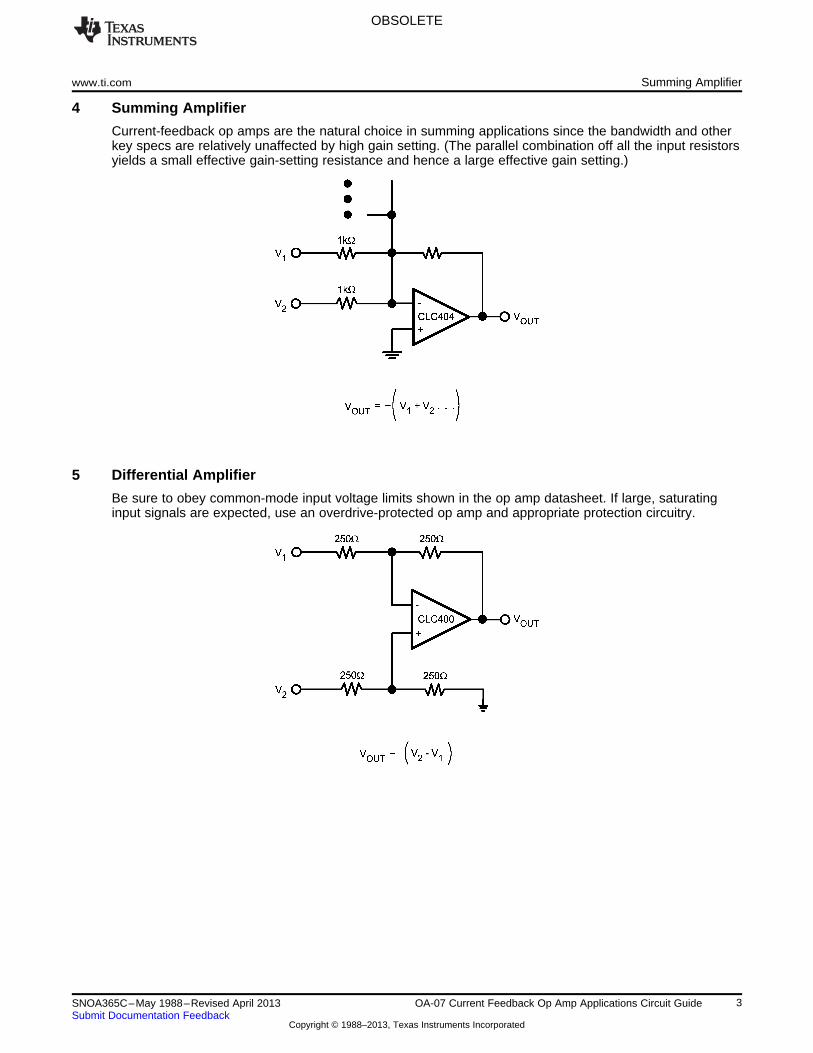
4 Summing Amplifier
Current-feedback op amps are the natural choice in summing applications since the bandwidth and otherkey specs are relatively unaffected by high gain setting. (The parallel combination off all the input resistorsyields a small effective gain-setting resistance and hence a large effective gain setting.)
5 Differential Amplifier
Be sure to obey common-mode input voltage limits shown in the op amp datasheet. If large, saturatinginput signals are expected, use an overdrive-protected op amp and appropriate protection circuitry.
3SNOA365C–May 1988–Revised April 2013 OA-07 Current Feedback Op Amp Applications Circuit GuideSubmit Documentation Feedback
Copyright © 1988–2013, Texas Instruments Incorporated
OBSOLETE
Differential Line Receiver www.ti.com
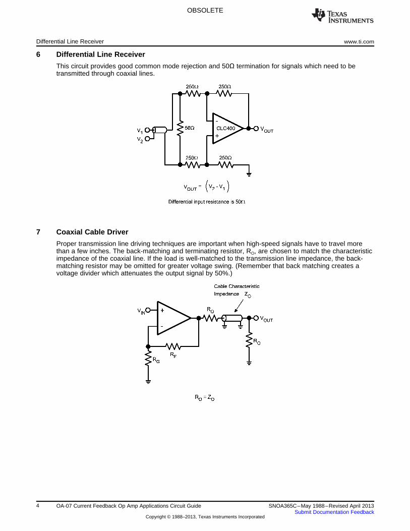
6 Differential Line Receiver
This circuit provides good common mode rejection and 50Ω termination for signals which need to betransmitted through coaxial lines.
7 Coaxial Cable Driver
Proper transmission line driving techniques are important when high-speed signals have to travel morethan a few inches. The back-matching and terminating resistor, RO, are chosen to match the characteristicimpedance of the coaxial line. If the load is well-matched to the transmission line impedance, the back-matching resistor may be omitted for greater voltage swing. (Remember that back matching creates avoltage divider which attenuates the output signal by 50%.)
4 OA-07 Current Feedback Op Amp Applications Circuit Guide SNOA365C–May 1988–Revised April 2013Submit Documentation Feedback
Copyright © 1988–2013, Texas Instruments Incorporated
OBSOLETE
www.ti.com Distribution Amplifier
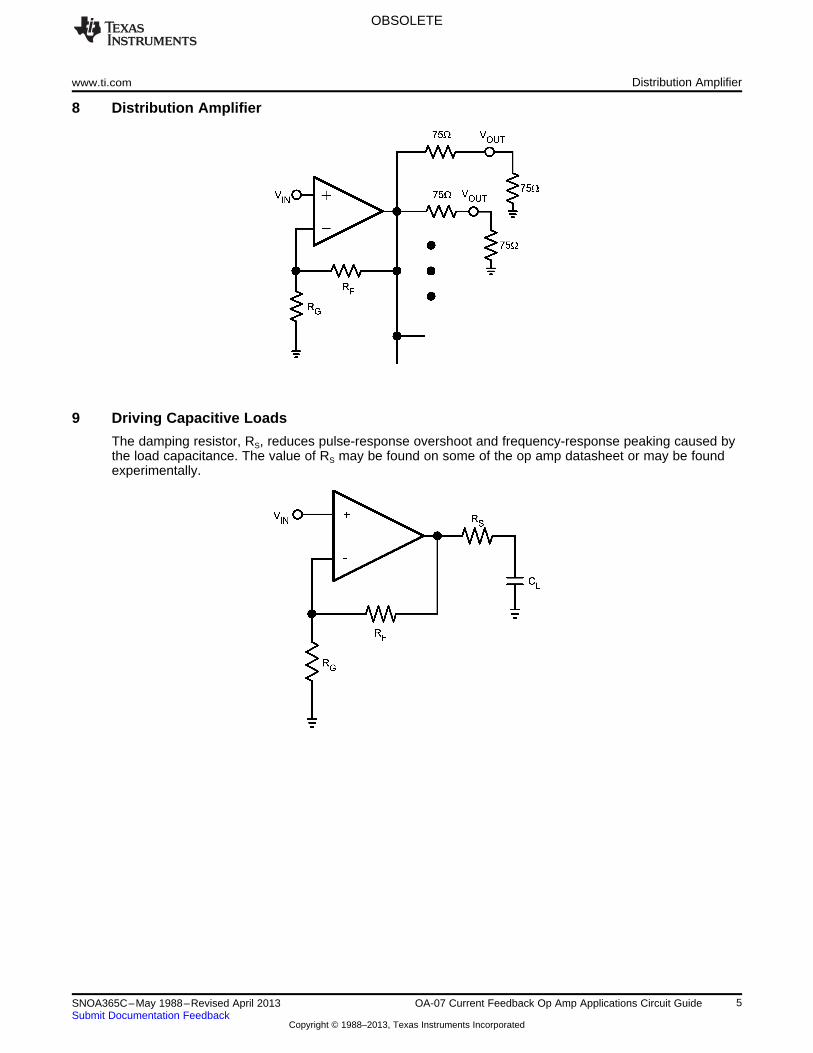
8 Distribution Amplifier
9 Driving Capacitive Loads
The damping resistor, RS, reduces pulse-response overshoot and frequency-response peaking caused bythe load capacitance. The value of RS may be found on some of the op amp datasheet or may be foundexperimentally.
5SNOA365C–May 1988–Revised April 2013 OA-07 Current Feedback Op Amp Applications Circuit GuideSubmit Documentation Feedback
Copyright © 1988–2013, Texas Instruments Incorporated
OBSOLETE
Output Current Booster www.ti.com
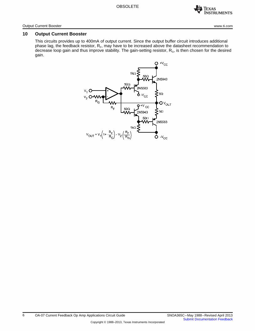
10 Output Current Booster
This circuits provides up to 400mA of output current. Since the output buffer circuit introduces additionalphase lag, the feedback resistor, RF, may have to be increased above the datasheet recommendation todecrease loop gain and thus improve stability. The gain-setting resistor, RG, is then chosen for the desiredgain.
6 OA-07 Current Feedback Op Amp Applications Circuit Guide SNOA365C–May 1988–Revised April 2013Submit Documentation Feedback
Copyright © 1988–2013, Texas Instruments Incorporated

OBSOLETE
www.ti.com Simple Offset Adjustment
11 Simple Offset Adjustment
The Zener diode biasing resistor, R, should be chosen to provide a diode current of 7.5mA.
7SNOA365C–May 1988–Revised April 2013 OA-07 Current Feedback Op Amp Applications Circuit GuideSubmit Documentation Feedback
Copyright © 1988–2013, Texas Instruments Incorporated

OBSOLETE
Composite Amplifier for Low Offset and Drift (#1) www.ti.com
12 Composite Amplifier for Low Offset and Drift (#1)
This composite circuit provides both high speed and good DC performance and unlike most compositecircuits, it provides good settling performance (17ns to 0.1%). In operation, the OP-27 op amp drives itsoutput such that the summing node is driven to 0V (which is the normal case for an inverting gain circuits).Thus, the circuit output takes on the high performance DC characteristics of the OP-27. At highfrequencies, the high-speed op amp takes over to provide good AC performance.
13 Composite Amplifier for Low Offset and Drift (#2)
This composite circuit is useful with those products which have the feedback resistor connected internallyto both the input and output. RB is adjusted for minimum output voltage at the OP-27 when VOUT is a70kHz square wave of 10VPP centered at 0V.
(1)
8 OA-07 Current Feedback Op Amp Applications Circuit Guide SNOA365C–May 1988–Revised April 2013Submit Documentation Feedback
Copyright © 1988–2013, Texas Instruments Incorporated
OBSOLETE
www.ti.com Non-Inverting Composite Amplifier
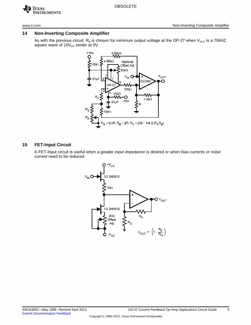
14 Non-Inverting Composite Amplifier
As with the previous circuit, RB is chosen for minimum output voltage at the OP-27 when VOUT is a 70kHZsquare wave of 10VPP center at 0V.
15 FET-Input Circuit
A FET-input circuit is useful when a greater input impedance is desired or when bias currents or noisecurrent need to be reduced.
9SNOA365C–May 1988–Revised April 2013 OA-07 Current Feedback Op Amp Applications Circuit GuideSubmit Documentation Feedback
Copyright © 1988–2013, Texas Instruments Incorporated

OBSOLETE
AC-coupled Amplifier (with Single-Supply Biasing) www.ti.com
16 AC-coupled Amplifier (with Single-Supply Biasing)
The voltage divider circuit at the non-inverting input biases the op amp input and output at the supplymidpoint. For those op amps having a bias pin, these pins should also connect to the supply midpoint biascircuit.
17 Reducing Bandwidth
Bandwidth and loop stability is controlled by RF. Increasing RF reduces bandwidth according to theapproximate relationship:
10 OA-07 Current Feedback Op Amp Applications Circuit Guide SNOA365C–May 1988–Revised April 2013Submit Documentation Feedback
Copyright © 1988–2013, Texas Instruments Incorporated

OBSOLETE
www.ti.com Adjustable Bandwidth
18 Adjustable Bandwidth
By increasing the inverting input impedance (which is normally very low) of a current feedback op amp,the bandwidth of the op amp can be reduced. The bandwidth of the circuit below can be varied over arange of 60MHz to 160MHz.
19 Reducing Frequency-Response Peaking
(due to stray capacitance in parallel with RG)
The low-pass filter at the non-inverting input cancels the frequency-response zero caused by CSTRAY. Atlow non-inverting gains, the CLC231 or CLC400 will provide a flatter frequency response without the needfor the low-pass filter (because they can be used with lower feedback resistor values).
11SNOA365C–May 1988–Revised April 2013 OA-07 Current Feedback Op Amp Applications Circuit GuideSubmit Documentation Feedback
Copyright © 1988–2013, Texas Instruments Incorporated

OBSOLETE
Adjustable Gain Using a FET www.ti.com
20 Adjustable Gain Using a FET
This circuit provides a 26dB adjustment range and a gain flatness of 1dB from DC to 50MHz. An SD210FET provides low on-resistance with minimal capacitive loading.
21 Adjustable Gain Using a Photoresistor
This circuit provides a 12dB adjustment range and a gain flatness of 1dB from DC to 20MHz. The 741circuit improves temperature stability and repeatability of the photoresistor circuit.
12 OA-07 Current Feedback Op Amp Applications Circuit Guide SNOA365C–May 1988–Revised April 2013Submit Documentation Feedback
Copyright © 1988–2013, Texas Instruments Incorporated

OBSOLETE
www.ti.com Integrator (#1)
22 Integrator (#1)
With current-feedback op amps, it is importance to keep large capacitance values out of the invertingfeedback loop in order to maintain stability.
(2)
23 Integrator (#2)
This integrator provides higher DC gain than #1. For values shown, the DC gain is 55dB. Higher valuescan be obtained by reducing RG, however, the ratio of RG to R1 should remain constant for adequate loopstability. Much of the output noise is directly proportional to R1 so that the higher DC gain is obtained atthe expense of higher noise. This circuit does not have the stability problem that is related to resistormatching as does integrator #1.
13SNOA365C–May 1988–Revised April 2013 OA-07 Current Feedback Op Amp Applications Circuit GuideSubmit Documentation Feedback
Copyright © 1988–2013, Texas Instruments Incorporated

OBSOLETE
Integrator with Zero www.ti.com
24 Integrator with Zero
In this circuit, feedback capacitance is acceptable because the op amp relies upon the value of thefeedback resistor for stability.
14 OA-07 Current Feedback Op Amp Applications Circuit Guide SNOA365C–May 1988–Revised April 2013Submit Documentation Feedback
Copyright © 1988–2013, Texas Instruments Incorporated
OBSOLETE
www.ti.com Active Filter Circuits
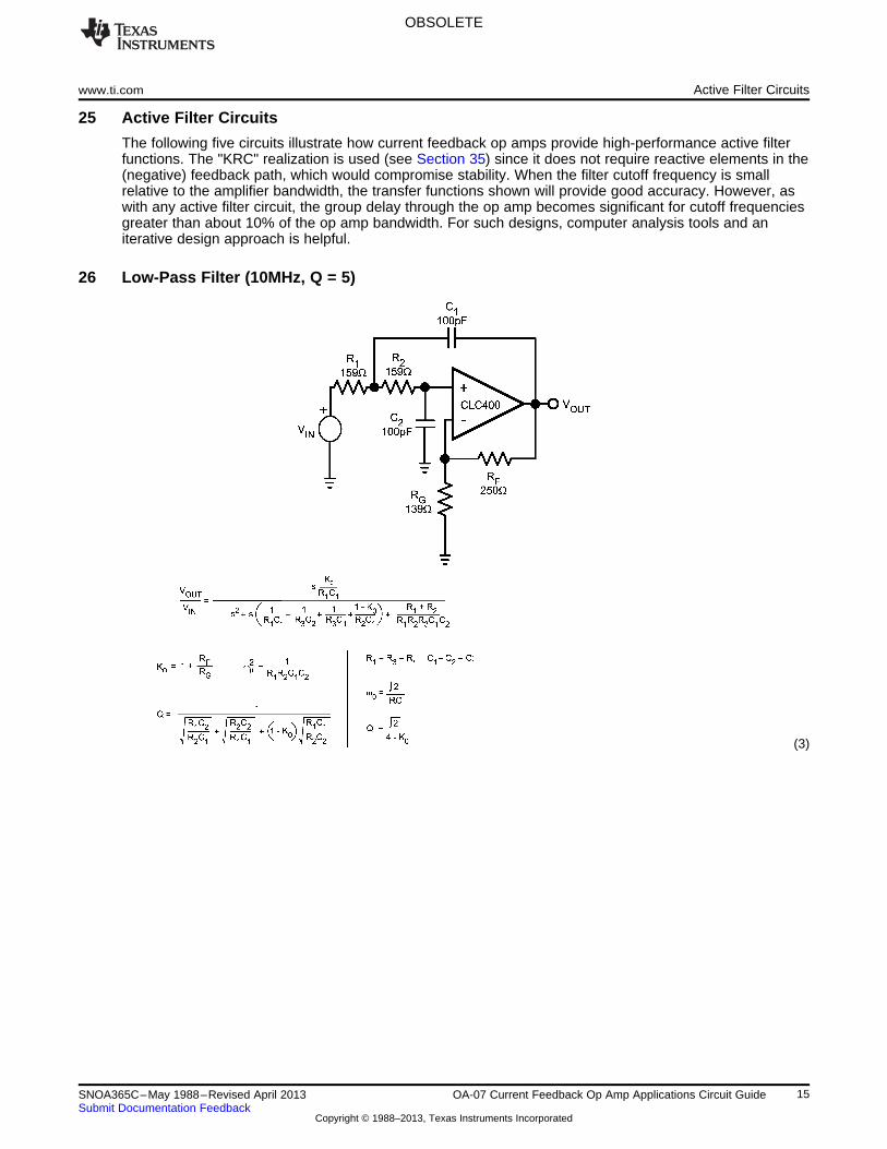
25 Active Filter Circuits
The following five circuits illustrate how current feedback op amps provide high-performance active filterfunctions. The "KRC" realization is used (see Section 35) since it does not require reactive elements in the(negative) feedback path, which would compromise stability. When the filter cutoff frequency is smallrelative to the amplifier bandwidth, the transfer functions shown will provide good accuracy. However, aswith any active filter circuit, the group delay through the op amp becomes significant for cutoff frequenciesgreater than about 10% of the op amp bandwidth. For such designs, computer analysis tools and aniterative design approach is helpful.
26 Low-Pass Filter (10MHz, Q = 5)
(3)
15SNOA365C–May 1988–Revised April 2013 OA-07 Current Feedback Op Amp Applications Circuit GuideSubmit Documentation Feedback
Copyright © 1988–2013, Texas Instruments Incorporated

OBSOLETE
High-Pass Filter (1MHz, Q = 2) www.ti.com
27 High-Pass Filter (1MHz, Q = 2)
(4)
16 OA-07 Current Feedback Op Amp Applications Circuit Guide SNOA365C–May 1988–Revised April 2013Submit Documentation Feedback
Copyright © 1988–2013, Texas Instruments Incorporated
OBSOLETE
www.ti.com Band-Pass Filter (40MHz, Q = 4)
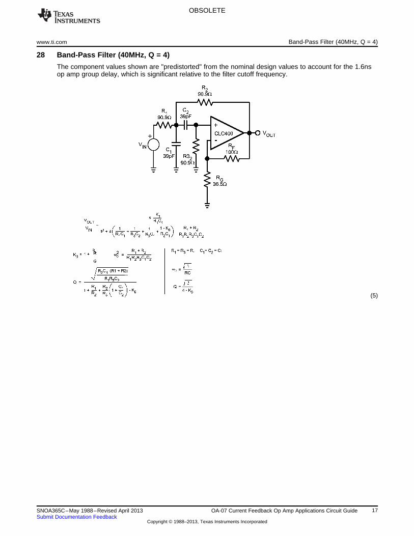
28 Band-Pass Filter (40MHz, Q = 4)
The component values shown are "predistorted" from the nominal design values to account for the 1.6nsop amp group delay, which is significant relative to the filter cutoff frequency.
(5)
17SNOA365C–May 1988–Revised April 2013 OA-07 Current Feedback Op Amp Applications Circuit GuideSubmit Documentation Feedback
Copyright © 1988–2013, Texas Instruments Incorporated
OBSOLETE
Band-Stop Filter (4MHz, Q = 4) www.ti.com
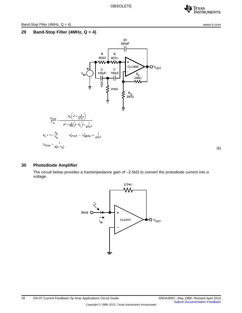
29 Band-Stop Filter (4MHz, Q = 4)
(6)
30 Photodiode Amplifier
The circuit below provides a transimpedance gain of –2.5kΩ to convert the protodiode current into avoltage.
18 OA-07 Current Feedback Op Amp Applications Circuit Guide SNOA365C–May 1988–Revised April 2013Submit Documentation Feedback
Copyright © 1988–2013, Texas Instruments Incorporated

OBSOLETE
www.ti.com D/A Converted Buffer Amplifier
31 D/A Converted Buffer Amplifier
Most high-speed, current-output D/A converters provide the best performance when driving little or no loadimpedance. The circuit below meets this requirement while also providing a transimpedance gain thatconverts the D/A output current into a Voltage. The variable capacitor in the feedback loop should beadjusted for desired pulse response to compensate for the D/A output capacitance, which otherwisecaused frequency-response peaking or instability. The 50Ω and 500Ω resistors reduce the effective valueof the feedback capacitance so that a reasonable value capacitor may be used.
For example, with the CLC401, RF = 2.5kΩ and a D/A output capacitance of 20pF, C ≅ 5pF.
32 Tunnel Diode Detector Amplifier
See the D/A converter buffer circuit for circuit highlights.
19SNOA365C–May 1988–Revised April 2013 OA-07 Current Feedback Op Amp Applications Circuit GuideSubmit Documentation Feedback
Copyright © 1988–2013, Texas Instruments Incorporated

OBSOLETE
Non-Linear Transfer Functions www.ti.com
33 Non-Linear Transfer Functions
Current-feedback op amps are particularly useful in non-linear transfer function circuits. Since bandwidthand other key specifications are independent of gain-the dynamic performance is relatively independent ofsignal level.
In analyzing the circuit, it is useful to identify the three input signal paths that contribute to the outputvoltage (the 1kΩ resistor and the two diode bridges). Each of these paths terminates at the invertinginput–a point that is at virtual ground. Due to feedback, the current through the feedback resistor is equalto the sum of these input currents. The output voltage, therefore, is the product of the feedback resistorand the sum of the input current.
The individual input currents are equal to the input voltage divided by the respective gain-setting resistor.However, in the signal paths containing the bridges, the current follows this linear relationship until it limitsat 12V/16kΩ. This is what leads to the non-linear gain. A more accurate analysis requires that the diodebulk and dynamic resistance be included.
20 OA-07 Current Feedback Op Amp Applications Circuit Guide SNOA365C–May 1988–Revised April 2013Submit Documentation Feedback
Copyright © 1988–2013, Texas Instruments Incorporated
OBSOLETE
www.ti.com Peak Detector
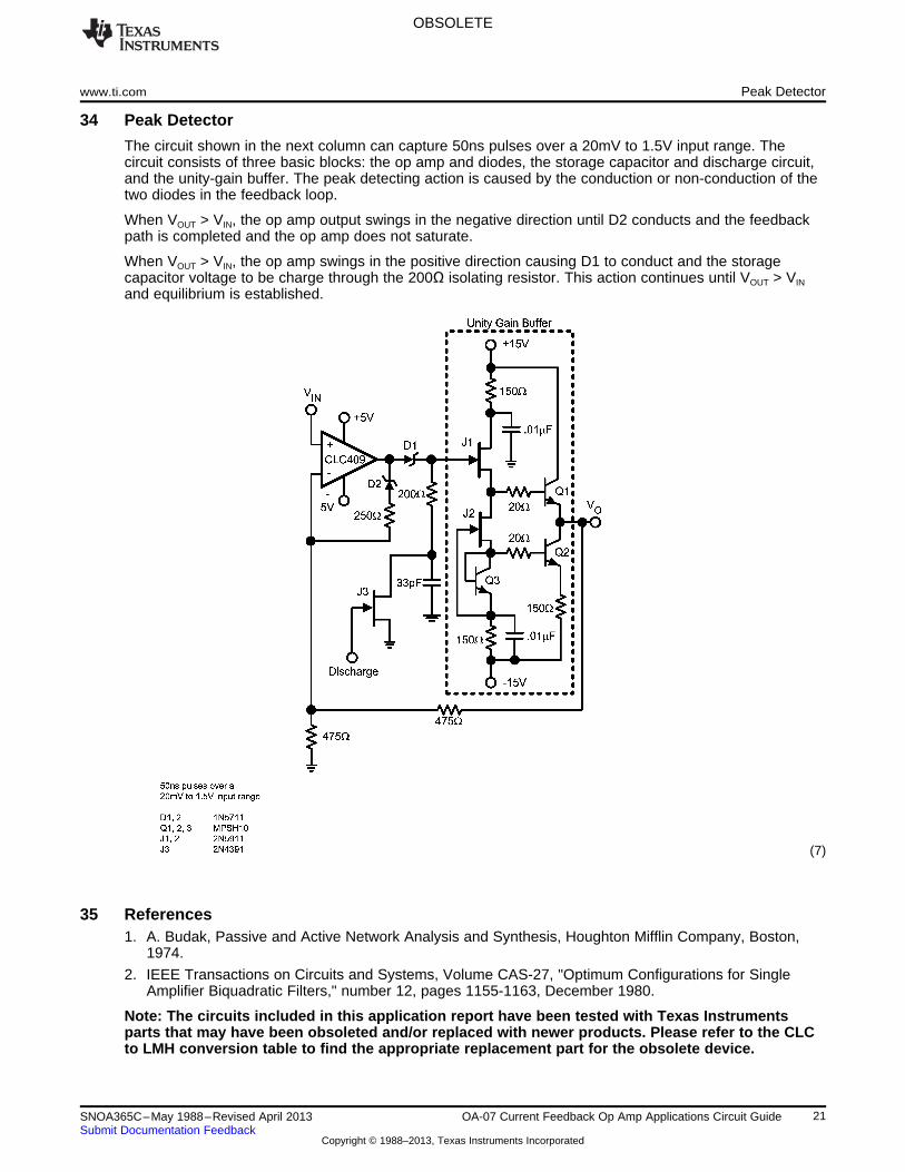
34 Peak Detector
The circuit shown in the next column can capture 50ns pulses over a 20mV to 1.5V input range. Thecircuit consists of three basic blocks: the op amp and diodes, the storage capacitor and discharge circuit,and the unity-gain buffer. The peak detecting action is caused by the conduction or non-conduction of thetwo diodes in the feedback loop.
When VOUT > VIN, the op amp output swings in the negative direction until D2 conducts and the feedbackpath is completed and the op amp does not saturate.
When VOUT > VIN, the op amp swings in the positive direction causing D1 to conduct and the storagecapacitor voltage to be charge through the 200Ω isolating resistor. This action continues until VOUT > VIN
and equilibrium is established.
(7)
35 References1. A. Budak, Passive and Active Network Analysis and Synthesis, Houghton Mifflin Company, Boston,
1974.
2. IEEE Transactions on Circuits and Systems, Volume CAS-27, "Optimum Configurations for SingleAmplifier Biquadratic Filters," number 12, pages 1155-1163, December 1980.
Note: The circuits included in this application report have been tested with Texas Instrumentsparts that may have been obsoleted and/or replaced with newer products. Please refer to the CLCto LMH conversion table to find the appropriate replacement part for the obsolete device.
21SNOA365C–May 1988–Revised April 2013 OA-07 Current Feedback Op Amp Applications Circuit GuideSubmit Documentation Feedback
Copyright © 1988–2013, Texas Instruments Incorporated

IMPORTANT NOTICE
Texas Instruments Incorporated and its subsidiaries (TI) reserve the right to make corrections, enhancements, improvements and otherchanges to its semiconductor products and services per JESD46, latest issue, and to discontinue any product or service per JESD48, latestissue. Buyers should obtain the latest relevant information before placing orders and should verify that such information is current andcomplete. All semiconductor products (also referred to herein as “components”) are sold subject to TI’s terms and conditions of salesupplied at the time of order acknowledgment.
TI warrants performance of its components to the specifications applicable at the time of sale, in accordance with the warranty in TI’s termsand conditions of sale of semiconductor products. Testing and other quality control techniques are used to the extent TI deems necessaryto support this warranty. Except where mandated by applicable law, testing of all parameters of each component is not necessarilyperformed.
TI assumes no liability for applications assistance or the design of Buyers’ products. Buyers are responsible for their products andapplications using TI components. To minimize the risks associated with Buyers’ products and applications, Buyers should provideadequate design and operating safeguards.
TI does not warrant or represent that any license, either express or implied, is granted under any patent right, copyright, mask work right, orother intellectual property right relating to any combination, machine, or process in which TI components or services are used. Informationpublished by TI regarding third-party products or services does not constitute a license to use such products or services or a warranty orendorsement thereof. Use of such information may require a license from a third party under the patents or other intellectual property of thethird party, or a license from TI under the patents or other intellectual property of TI.
Reproduction of significant portions of TI information in TI data books or data sheets is permissible only if reproduction is without alterationand is accompanied by all associated warranties, conditions, limitations, and notices. TI is not responsible or liable for such altereddocumentation. Information of third parties may be subject to additional restrictions.
Resale of TI components or services with statements different from or beyond the parameters stated by TI for that component or servicevoids all express and any implied warranties for the associated TI component or service and is an unfair and deceptive business practice.TI is not responsible or liable for any such statements.
Buyer acknowledges and agrees that it is solely responsible for compliance with all legal, regulatory and safety-related requirementsconcerning its products, and any use of TI components in its applications, notwithstanding any applications-related information or supportthat may be provided by TI. Buyer represents and agrees that it has all the necessary expertise to create and implement safeguards whichanticipate dangerous consequences of failures, monitor failures and their consequences, lessen the likelihood of failures that might causeharm and take appropriate remedial actions. Buyer will fully indemnify TI and its representatives against any damages arising out of the useof any TI components in safety-critical applications.
In some cases, TI components may be promoted specifically to facilitate safety-related applications. With such components, TI’s goal is tohelp enable customers to design and create their own end-product solutions that meet applicable functional safety standards andrequirements. Nonetheless, such components are subject to these terms.
No TI components are authorized for use in FDA Class III (or similar life-critical medical equipment) unless authorized officers of the partieshave executed a special agreement specifically governing such use.
Only those TI components which TI has specifically designated as military grade or “enhanced plastic” are designed and intended for use inmilitary/aerospace applications or environments. Buyer acknowledges and agrees that any military or aerospace use of TI componentswhich have not been so designated is solely at the Buyer's risk, and that Buyer is solely responsible for compliance with all legal andregulatory requirements in connection with such use.
TI has specifically designated certain components as meeting ISO/TS16949 requirements, mainly for automotive use. In any case of use ofnon-designated products, TI will not be responsible for any failure to meet ISO/TS16949.
Products Applications
Audio www.ti.com/audio Automotive and Transportation www.ti.com/automotive
Amplifiers amplifier.ti.com Communications and Telecom www.ti.com/communications
Data Converters dataconverter.ti.com Computers and Peripherals www.ti.com/computers
DLP® Products www.dlp.com Consumer Electronics www.ti.com/consumer-apps
DSP dsp.ti.com Energy and Lighting www.ti.com/energy
Clocks and Timers www.ti.com/clocks Industrial www.ti.com/industrial
Interface interface.ti.com Medical www.ti.com/medical
Logic logic.ti.com Security www.ti.com/security
Power Mgmt power.ti.com Space, Avionics and Defense www.ti.com/space-avionics-defense
Microcontrollers microcontroller.ti.com Video and Imaging www.ti.com/video
RFID www.ti-rfid.com
OMAP Applications Processors www.ti.com/omap TI E2E Community e2e.ti.com
Wireless Connectivity www.ti.com/wirelessconnectivity
Mailing Address: Texas Instruments, Post Office Box 655303, Dallas, Texas 75265Copyright © 2013, Texas Instruments Incorporated