ny 11973-5000 - bnl.gov · signed to read out signals from a pixelated silicon drift detector...
TRANSCRIPT

Pres. 2007 Nuclear Science Symp. Honolulu, HI, 10/27-I 1/3/2007
BNL- 7 9 5 5 8- 2 0 0 7 - C P
FRONT-END ASIC FOR HIGH RESOLUTION X-RAY SPECTROMETERS*
Gianluigi De Geronimo, Wei Chen, Jack Fried, Zheng Li, Donald A. Pinelli, Pave1 Rehak, and Emerson Verson
Brookhaven National Laboratory Upton, NY 11973-5000
* * *
Jessica A. Gaskin and Brian D. Ramsey
Marshall Space Flight Center Huntsville, AL
* * *
Giovanni Anelli
LEM SA Plans-les-Ouates, Geneva, Switzerland
October, 2007
*This manuscript has been authored by Brookhaven Science Associates, LLC under Contract No. DE-AC02-98CH10886 with the U.S. Department of Energy. The United States Government retains, and the publisher, by accepting the article for publication, acknowledges, a world-wide license to publish or reproduce the published form of this manuscript, or allow others to do so, for the United States Government purposes.

DISCLAIMER
This work was prepared as an account of work sponsored by an agency of the United States Government. Neither the United States Government nor any agency thereoJI nor any of their employees, nor any of their contractors, subcontractors, or their employees, makes any warranty, express or implied, or assumes any legal liability or responsibility for the accuracy, completeness, or any third party's use or the results of such use of any information, apparatus, product, or process disclosed, or represents that its use would not infringe privately owned rights. Reference herein to any specific commercial product, process, or service by trade name, trademark, manufacturer, or otherwise, does not necessarily constitute or imply its endorsement, recommendation, or favoring by the United States Government or any agency thereof or its contractors or subcontractors. The views and opinions of authors expressed herein do not necessarily state or reflect those of the United States Government or any agency thereo$
Front-end ASIC for High Resolution X-Ray Spectrometers
Gianluigi De Geronimo, Wei Chen, Jack Fried, Zheng Li, Donald A. Pinelli, Pave1 Rehak, Emerson Vernon, Jessica A. Gaskin, Brian D. Ramsey, and Giovanni Anelli
Abstract -- We present an application specific integrated circuit (ASIC) for high-resolution x-ray spectrometers. The ASIC is de- signed to read out signals from a pixelated silicon drift detector (SDD). Each hexagonal pixel has an area of 15 mmz and an anode capacitance of less than 100 fF. There is no integrated Field Effect transistor (FET) in the pixel, rather, the readout is done by wire- bonding the anodes to the inputs of the ASIC. The ASIC provides 14 channels of low-noise charge amplification, high-order shaping with baseline stabilization, and peak detection with analog mem- ory. The readout is sparse and based on low voltage differential signaling. An interposer provides all the interconnections required to bias and operate the system. The channel dissipates 1.6 mW. The complete 14-pixel unit covers an area of 210 mm’, dissipates 12 mW cm-’, and can be tiled to cover an arbitrarily large detec- tion area. We measured a preliminary resolution of 172 eV at -35 C on the 6 keV peak of a 55Fe source.
I. INTRODUCTION The work discussed here is part of a joint effort between the
NASA Marshall Space Flight Center (MSFC) and Brookhaven National Laboratory (BNL) to develop a prototype high- resolution x-ray spectrometer (XRS) able to measure the abun- dances of light elements fluoresced by ambient radiation. There are two possible uses being explored for this effort. The first application involves mapping the lunar surface from a low- altitude orbiter [1,2]. The second application is mapping the elemental composition of the surface of Europa [2,3].
A lunar mission requires a detector area of 500 cm2, and able to offer an energy resolution better than 170 eV at 2 keV for rates up to few thousand counts s” cm-’ in a power budget of 20 mW cm-’. The Europa application requires a detector area of 10 cm’, and able to offer an energy resolution better than 130 eV at 280 eV for rates up to one million of counts s-’ cm-’ in a power budget of 80 mW cm.’. Detector cooling, not included in the power budget, can be provided in both cases for operations
The stringent requirements on the detector’s area, resolution, rate, and power suggest either using standard silicon diodes with high pixelation (a pixel area of few hundred pm’) and bump-bonded front-end electronics, or employing silicon drift detectors (SDDs) [4], [5] with moderate pixelation (a pixel area of few tens of mm’) and wire-bonded fiont-end electronics. As discussed in the next Section, the latter solution appears more attractive in terms of resolution, interconnects, and charge shar-
Other research groups reported promising results in terms of rate and resolution with pixelated SDDs with the input transis- tor (e.g. junction field effect transistor, JFET) integrated with each pixel [8-131. However, intergrating the FET imposes an additional technological challenge, might impose a lower limit
down to -35 C.
ing.
G. De Geronimo, W. Chen, J. Fried, Z. Li, D. A. Pinelli, and E. Vernon are with the In- strumentation Division, Brookhaven National Laboratory, Upton, NY. J. A. Gaskin and B. D. Ramsey are with the Marshall Space Flight Center, Huntsville, AL. G. Anelli was with CERN, Geneva, Switzerland. He is now with LEM SA, Plans-les- Ouates, Geneve, Switzerland.
in the power dissipation (some mW in the JFET itself), and requires somewhat higher complexity in the fiont-end electron- ics and interconnects to achieve the required stability, espe- cially at high count rates [14-201.
We propose an XRS prototype based on a pixelated SDD sensor without an integrated FET. The anodes of the SDD array are directly wire-bonded to the inputs of the low-noise multi- channel application specific integrated circuit (ASIC) as pre- sented here.
In Section I1 we discuss the criteria for choosing the sensor, and in Section I11 we introduce the detector’s architecture. Sec- tion IV illustrates the ASIC architecture along with some details of the circuit. Section V reports some preliminary experimental results.
11. CRITERIA FOR SELECTING THE SENSOR
To be compatible with both the lunar and Europa applica- tions the X R S must satisfy the following requirements: area 500 cm’, resolution 130 eV at 280 eV, and rate 1 Mcps/cm’, with a power budget of 20 mWIcm’. An advantage for both cases is that the XRS can be operated at temperatures down to -35 C.
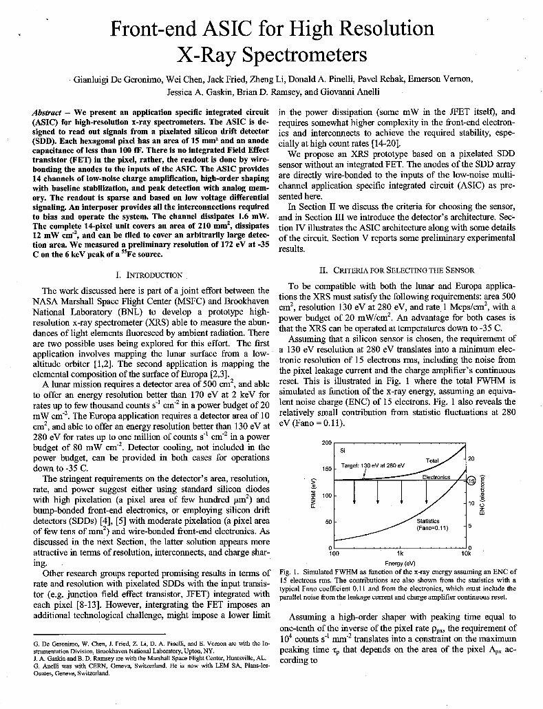
Assuming that a silicon sensor is chosen, the requirement of a 130 eV resolution at 280 eV translates into a minimum elec- tronic resolution of 15 electrons rms, including the noise fiom the pixel leakage current and the charge amplifier’s continuous reset. This is illustrated in Fig. 1 where the total FWHM is simulated as fimction of the x-ray energy, assuming an equiva- lent noise charge (ENC) of 15 electrons. Fig. 1 also reveals the relatively small contribution fiom statistic fluctuations at 280 eV (Fano = 0.1 1).
200 I I si n
Statistics (Fano=O.ll)
100 I k 10k Energy (eV)
Fig. 1. Simulated FWHM as hnction of the x-ray energy assuming an ENC of 15 electrons rms. The contributions are also shown fiom the statistics with a typical Fano coefficient 0.1 1 and fiom the electronics, which must include the parallel noise ffom the leakage current and charge amplifier continuous reset.
Assuming a high-order shaper with peaking time equal to one-tenth of the inverse of the pixel rate pP, the requirement of io4 counts s-’ mm-’ translates into a constramt on the maximum peaking time rP that depends on the area of the pixel Apx ac- cording to
For example, for a pixel of 10 mm' the peaking time should not exceed 1 ps.
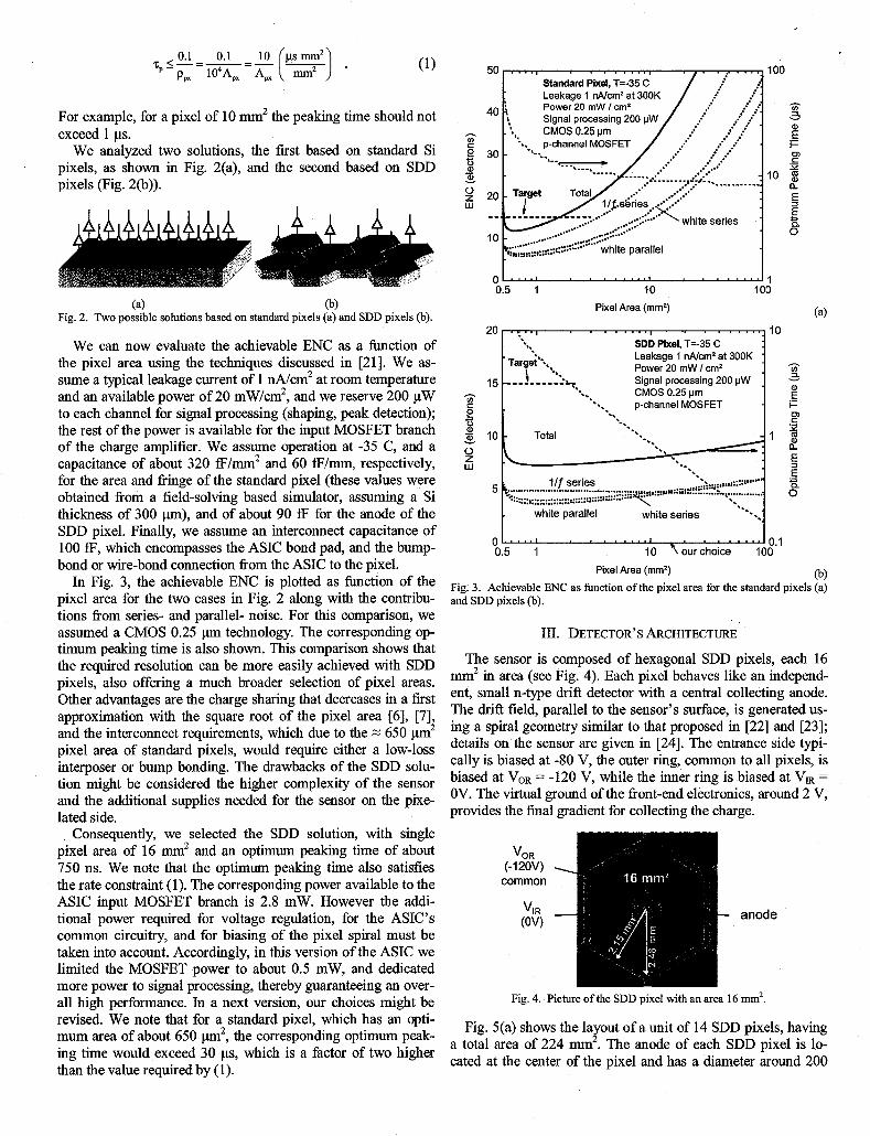
We analyzed two solutions, the first based on standard Si pixels, as shown in Fig. 2(a), and the second based on SDD pixels (Fig. 2(b)).
20 ' ".,' ' I .... I
SDD Pixel, T=-35 C Leakage I nA/cmZ at 300K Power 20 mW I cmz Signal processing 200 WW CMOS 0.25 Wm
. Targei't \ '*-,,
--.. p-channel MOSFET -. 15 _________:
h .. v) K
'- -. e +
( 4 (b) Fig. 2. Two possible solutions based on standard pixels (a) and SDD pixels (b).
We can now evaluate the achievable ENC as a function of the pixel area using the techniques discussed in [21]. We as- sume a typical leakage current of 1 nA/cm' at room temperature and an available power of 20 mWIcm', and we reserve 200 pW to each channel for signal processing (shaping, peak detection); the rest of the power is available for the input MOSFET branch of the charge amplifier. We assume operation at -35 C, and a capacitance of about 320 fFlmm2 and 60 fFlmm, respectively, for the area and fiinge of the standard pixel (these values were obtained fiom a field-solving based simulator, assuming a Si thickness of 300 pm), and of about 90 fF for the anode of the SDD pixel. Finally, we assume an interconnect capacitance of 100 E, which encompasses the ASIC bond pad, and the bump- bond or wire-bond connection fiom the ASIC to the pixel.
In Fig. 3, the achievable ENC is plotted as function of the pixel area for the two cases in Fig. 2 along with the contribu- tions fiom series- and parallel- noise. For this comparison, we assumed a CMOS 0.25 pm technology. The corresponding op- timum peaking time is also shown. This comparison shows that the required resolution can be more easily achieved with SDD pixels, also offering a much broader selection of pixel areas. Other advantages are the charge sharing that decreases in a first approximation with the square root of the pixel area [6], [7], and the interconnect requirements, which due to the = 650 pm2 pixel area of standard pixels, would require either a low-loss interposer or bump bonding. The drawbacks of the SDD solu- tion might be considered the higher complexity of the sensor and the additional supplies needed for the sensor on the pixe- lated side.
Consequently, we selected the SDD solution, with single pixel area of 16 mm2 and an optimum peaking time of about 750 ns. We note that the optimum peaking time also satisfies the rate constraint (1). The corresponding power available to the ASIC input MOSFET branch is 2.8 mW. However the addi- tional power required for voltage regulation, for the ASIC's common circuitry, and for biasing of the pixel spiral must be taken into account. Accordingly, in this version of the ASIC we limited the MOSFET power to about 0.5 mW, and dedicated more power to signal processing, thereby guaranteeing an over- all high performance. In a next version, our choices might be revised. We note that for a standard pixel, which has an opti- mum area of about 650 pm', the corresponding optimum peak- ing time would exceed 30 ps, which is a factor of two higher than the value required by (1).
10
- - u) a v
E - i =
m
... '., -. white parallel white series
c l/f series ...... ................................................... *,..b',,: ...... ..... :..
7 .-
111. DETECTOR'S ARCHITECTURE
The sensor is composed of hexagonal SDD pixels, each 16 mm2 in area (see Fig. 4). Each pixel behaves like an independ- ent, small n-type drift detector with a central collecting anode. The drift field, parallel to the sensor's surface, is generated us- ing a spiral geometry similar to that proposed in [22] and [23]; details on the sensor are given in [24]. The entrance side typi- cally is biased at -80 V, the outer ring, common to all pixels, is biased at VoR = -120 V, while the inner ring is biased at VR = OV. The virtual ground of the fiont-end electronics, around 2 V, provides the final gradient for collecting the charge.
VOR (-12OV) common
VIR anode (OV)
Fig. 4. Picture of the SDD pixel with an area 16 mm2
Fig. 5(a) shows the layout of a unit of 14 SDD pixels, having a total area of 224 mm'. The anode of each SDD pixel is lo- cated at the center of the pixel and has a diameter around 200
pm (Fig. 4). The pixelated side of the unit is attached to one side of an interposer with a zz 2 mm hole in correspondence with each anode. There is a 1Cchannel ASIC on the other side of the interposer. Each anode is wire-bonded through the holes to one input of the 14 channels of the ASIC, as shown in Fig 5(b). Through the same holes the inner ring of the pixel is wire- bonded to the line that provides VR (depicted by the small dot near each hole in Fig. 5(b). One additional hole, in the upper left, provides the wire bond for VoR. It can be easily verified that the resulting 14-element SDD-ASIC unit can be tiled to cover an arbitrarily large sensitive area. Since the ASIC dissi- pates about 25 mW, this represents 25 mW I 224 mm2 = 11 mWlcm2, a value well within the requirement for the applica- tion.
( 4 (b) Fig. 5. Layout of the unit of 14 SDD pixels (a), with total area 224 mm', and picture of the interposer (b) with the SDD unit attached on the back side, with the ASIC, measuring 2 x 4.6 mm2, attached on the front side. The 14 inputs of the ASIC are wire-bonded to the pixel anodes through 2 mm holes.
The electrons generated by the ionizing event are collected by the anode and read out by the ASIC that performs low-noise charge amplification, filtering, discrimination, peak detection with analog memory, and sparse readout. In the next Section, we describe the architecture of the ASIC.
Iv . ARCHITECTURE OF THE ASIC
Fig. 6 is a block diagram illustrating the architecture of the ASIC. The ASIC implements 14 front-end channels, multiplex- ers, common bias circuitry, registers, DACs, and control and readout logic.
; dual-stage charge amplifier
I
ENA CLK
PDO
FLG
ADR
MON mux
Fig. 6. Block diagram of the ASIC.
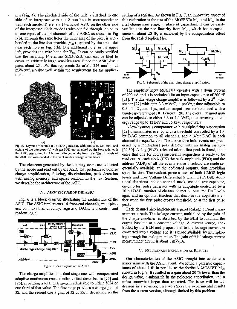
The charge amplifier is a dual-stage one with compensated adaptive continuous reset, similar to that described in [25] and [26], providing a total charge-gain adjustable to either 1024 or one third of that value. The fist stage provides a charge gain of 32, and the second one a gain of 32 or 3213, depending on the
setting of a register. As shown in Fig. 7, an innovative aspect of this realization is the use of the MOSFETs Mcl and Ma in the first charge gain stage, in place of capacitors. It can be easily verified that the non-linearity fiom Mcl, which has a capaci- tance of about 20 fF, is canceled by the compensation effect from the scaled replica Mcz.
CZ CPNZ II II ,
to shaper
- from
anode Fig. 7. Schematic ofthe dual-stage charge amplification.
The amplifier input MOSFET operates with a drain current of 200 yA and it is optimized for an input capacitance of 200 fF [21]. The dual-stage charge amplifier is followed by a 5'h order shaper [27] with gain 3.3 mV/E, a peaking time adjustable to 0.5-, I-, 2-, and 4-p, and an output baseline stabilized with a band-gap-referenced BLH circuit [28]. The overall channel gain can be adjusted to either 3.3 or 1.1 VIE, thus covering an en- ergy range up to 12 keV and 36 keV, respectively.
A low-hysteresis comparator with multiple-firing suppression [29] discriminates events, with a threshold controlled by a 10- bit DAC common to all channels, and a 3-bit DAC in each channel for equalization. The above-threshold events are proc- essed by a multi-phase peak detector with an analog memory [29,30]. A flag (FLG), released after a first peak is found, indi- cates that one (or more) successhl acquisition is ready to be read out. At each clock (CK) the peak amplitude (PDO) and the address (ADR) of all the events above threshold are made se- quentially available at the dedicated outputs, thus providing sparsification. The readout process uses of both CMOS logic levels and Low Voltage Differential Signaling (LVDS). Addi- tional fimctions include channel mask, channel test capacitor, on-chip test pulse generator with its amplitude controlled by a 10-bit DAC, monitor of channel shaper outputs and DAC volt- ages, and an optional h c t i o n that disables the acquisition ei- ther when the first pulse crosses threshold, or at the first pulse peak.
Each channel also implements a pixel leakage current meas- urement circuit. The leakage current, multiplied by the gain of the charge amplifier, is absorbed by the BLH to maintain the output baseline at a constant voltage. A current source, con- trolled by the BLH and proportional to the leakage current, is converted into a voltage and it is made available by multiplex- ing through the analog monitor. The gain of this leakage current measurement circuit is about 1 mV1pA.
v. PRELIMINARY EXPERIMENTAL RESULTS
Our characterization of the ASIC brought into evidence a major issue with the ASIC layout. We found a parasitic capaci- tance of about 4 fF in parallel to the feedback MOSFET Wl shown in Fig. 7. It resulted in a gain about 20 % lower than the design value, a mismatch in the pole-zero cancellation, and a noise somewhat larger than expected. The issue will be ad- dressed in a revision; here we report the experimental results from the current version, although limited by this problem.

Fig. 8 shows the simulated- (lines) and measured- (symbols) ENC as function of the peaking time. The blue triangles and red circles represent measurements taken with the rms voltmeter connected to the analog monitor of the channel. The black dia- monds signify measurements from a test pulse set at 0.3 fC (6.75 kev). All measurements were done at -35 C.
The blue triangles correspond to the case where the sensor was not connected to the input and with the internal 1.6 pA in- put current generator enabled. The blue line is the correspond- ing simulation; the difference between them is mainly due to the lower gain, with consequent increase of the contribution fiom the shaper.
The red circles correspond to the case with the sensor con- nected to the input and biased. The internal 1.6 pA input current generator is disabled. A leakage current of about 2.6 pA was extracted, and directly confirmed by measurements using the leakage current measurement circuit. The red line is the corre- sponding simulation, shown in Fig. 8 with the dominant noise contributions, viz., charge amplifier, leakage current (this in- cludes the reset current), and shaper. In correspondence with the input capacitive load only the contribution from the charge am- plifier increases, while the shaper’s contribution remains the same (assuming a negligible drop in the gain with the input capacitive load).
The black diamonds are measurements acquired using the complete signal processing chain, i.e., encompassing the dis- criminator, peak detector, and multiplexing as described in the previous Section. The additional noise contribution is mainly related to the increase in current through the reset MOSFET during the discharge of the feedback capacitor after an event; it depends on the injected charge Qm (Le., the energy of the event) [25]. In this case, the increase is of the order of 5.5 e‘ rms at 0.3 fC (6.75 kev) although it is expected to be negligible at the few hundred eV spectral lines.
25
T = -35 C 0 16 mmz SDD pixel biased (120 fF, 2.6 PA) .
- v No SDD pixel (internal 1.6 PA) - + ... with pulse at 0.3 fC (6.7 keV), 20 kcps
I
0.1 1 10 Peaking Time [PSI
Fig. 8. Simulated and measured ENC versus peaking time without the sensor and with sensor connected and biased. The measurement with the test pulse peak at 6 keV is included. The dominant contributions to the ENC also are shown.
In Fig. 9 illustrates the ENC versus injected charge Qm (en- ergy equivalent in Si), measured using the test pulse at 0.5 ps peaking time. The increase appears negligible when compared with the statistical fluctuations in the charge generated by the ionizing events, also depicted in Fig. 9. It can be seen that, due to the discussed = 20 % deficit in gain, a charge corresponding
to 16 keV could be injected, despite the design limit, at this gain setting, being just above 12 keV. An integral linearity error be- low +/- 0.4% was measured over the entire signal range of 2V.
30 . I . , . I . , . , . , . , . , .-Total ENC
0 0 2 4 6 8 10 12 14 16
Energy [key Fig. 9. ENC versus injected charge (energy equivalent in Si) measured using the test pulse. The simulated contribution due to statistical fluctuations (Fano limited), and the corresponding total ENC are included.
Fig. 10 shows the spectrum fiom an uncollimated 55Fe source, measured at - 35 C, using the whole system with a peaking time of 1 ps, and a rate of 20 kcps. A resolution of 172 eV at 69.5 keV is observed, corresponding to 20.5 e-. The con- tribution from the electronics is about 14.3 e-, while Fano (0.1 1) contributes with 13.4 e-. The residual 6.0 e-, related to the sen- sor, still is being investigated.
Fig. 10 also illustrates a peak to background ratio of about 300 that was limited, in large amount, by charge sharing be- tween the SDD pixels.
SDD pixel 16 mm2 Fe, T = -35C
Rate = 20 kcps (electronics 14.3 e-)
1 0 2 4 6 8 10
Energy (keV) Fig. 10. Spectrum at -35 C, kom a 55Fe source measured with a peaking time of 1 ps, and a rate of 20 kcps.
Fig. 1 l(a) shows the spectra of 55Fe at different rates ranging from 20 kcps up to 400 kcps, measured with a peaking time of 0.5 ps. There is considerable degradation at 400 kcps. Fig. 1 l(b) shows the corresponding FWHM for 0.5- and 1-ps peak- ing time. These measurements are affected by the poor pole- zero cancellation and are expected to improve in a revision.
We note that, given the pixel area of 16 mm’, the require- ment of 1 Mcps/cm’ translates into about 150 kcpdpixel. At this rate, a resolution on the order of 170 keV at 6 keV appears achievable in a revision.

Fe 55
T = -35C Peaktime 0.5 p s
10kk . I - I . I . 1 ’ 1 ’
: SDD Dixel 16 mm2
I k :
100 :
10 :
1 - 0 2 4 6 8 10 12 14
Energy (keV)
I I I I A
600 - SDD pixel 16 mmz
500 - =Fe
- 400 - 3
I I I I 1 A
600 - SDD pixel 16 mmz
500 - =Fe
- 400 - 3
l o o / , I 1 1 , !target
I , ‘ I 0 0 100 200 300 400
Rate (kcps) Fig. 11. Spectrum (a) at -35 C, from a 55Fe source measured with a peaking time 0.5 ys, at rates fiom of 20- to 400-kcps; FWHM (b), at the k, spectral line, with peaking times of0.5- and 1-ys.
VI. CONCLUSIONS AND FUTURE WORK
We developed and characterized the first prototype of a high resolution x-ray spectrometer, based on SDD pixels with direct readout through a low-noise ASIC, has been developed and characterized. Promising resolution was obtained. The ASIC requires a revision to eliminate some parasitic effects affecting the gain and pole-zero cancellation. With the current system, cooled at -35 C, resolutions of 173 eV and 200 eV at 59.5 keV can be achieved at pixel rates of 20 kcps and 150 kcps respec- tively.
ACKNOWLEDGMENTS
The authors are grateful to Kim Ackley, Rolf Beuttenmuller, and John Triolo, from BNL, for the continuous assistance with the development. The authors are also indebted to Jeffrey Keis- ter and Peter D. Siddons, from the NSLS and Albert0 Fazzi, from Milan Polytechnic. A special acknowledgment goes to Avril D. Woodhead for assistance with editing.
This manuscript has been authored by employees of Brook- haven Science Associates, LLC under Contract No. DE-AC02- 98CH10886 with the U.S. Department of Energy. The publisher by accepting the manuscript for publication acknowledges that the United States Government retains a non-exclusive, paid-up,
irrevocable, world-wide license to publish or reproduce the published form of this manuscript, or allow others to do so, for United States Government purposes.
REFERENCES
[ 11 http://lro.larc.nasa.gov/ [2] M. W. Davidson “Moon rocks under the microscope,” (Oct. 2001), available at http://micro.magnet.fsu.edu/publications/pagesrocks.html. [3] http://sse.iul.nasa.gov/missionsprofile.cfm?MCode=EGE [4] E. Gatti and P. Rehak, “Semiconductor drift chamber - an application of a novel charge transport scheme”, Nucl. Insfrum. Mefh. 225, pp. 608-614,1984. [5] E. Gatti and P. Rehak, “Review of semiconductor drift detectors”, Nucl. Insfrum. Meth. 541, pp. 47-60,2005. [6] C. Rossington Tull, B. A. Ludewigt, and D. Lewak, “Spectral response of mulit-element silicon X-ray detectors”, IEEE Trans. Nucl. Sci., vol. 45, pp. 421 - 426,2002. [7] K. Mathieson, M. S. Passmore, P. Seller, M. L. Prydderch, V. O’Shea, R. L. Bates, K. M. Smith, and M. Rahman, “Charge sharing in silicon pixel detectors”, Nucl. Insfrum. Meth., A 487, pp. 113-122,2002. [8] C. Fiorini, A. Longoni, F. Perotti, C. Labanti, E. Rossi, P. Lechner, H. Soltau, and Lothar Struder, “A monolithic array of silicon drift detectors for high-resolution gamma-ray imaging”, IEEE Trans. Nucl. Sci., vol. 49, pp. 995- 1000,2002. [9] J. Sonsky, R. Koomneef, J. Huizenga, R. W. Hollander, L. K. Nanver, T. Scholtes, F. Roozenboom, and C. W. E, van Eijk, “Novel low-temperature processing of low-noise SDDs with ondetector electronics”, Nucl. Insfrum. Mefh., 517, pp. 301-312,2004. [lo] P. Lechner, C. Fiorini, A. Longoni, G. Lutz, A. Pahlke, H. Soltau, and L. Struder, “Silicon drift detectors for high resolution, high count rate X-ray spectroscopy at room temperature”, Advances in X-ray Analysis, vol. 47, pp. 53- 58,2004 [l 11 T. Eggert, 0. Boslau, P. Goldstrass, and J. Kemmer, ”Silicon drift detectors with enlarged sensitivity areas”, X-Ray Specfrometry, vol. 33, pp. 246-252, 2004. [12] W. Metzger, J. Engdahl, W. Rossner, 0. Boslau, and J. Kemmer, ”Large- area silicon drift detectors for new applications in nuclear medicine imaging”, IEEE Trans. Nucl. Sci., vol. 51,pp. 1631-1635,2004. [13] A. Longoni, C. Fiorini, C. Guazzoni, S. Buzzetti, M. Bellini, L. Struder, P. Lechner, A. Bjeoumikhov, and J. Kemmer, “XRF spectrometers based on monolithic arrays of silicon drift detectors: elemental mapping analyses and advanced detector structures”, IEEE Trans. Nucl. Sci., vol. 53, pp. 641-647, 2006. [ 141 C. Fiorini and P. Lechner, “Charge-sensitive preamplifier with continuous reset by means of the gate-to-drain current of the JFET integrated on the detector”, IEEE Trans. Nucl. ScL, vol. 49, no.3, pp. 1147-1151, Jun. 2002. [15] K. Hansen and C. Recklenben, “Spectral peak shift of Si-drift detectors with integrated JFET”, IEEE Trans. Nucl. Sci., vol. 51, pp. 1283-1288, Jun. 2004. [16] C. Fiorini, “A charge sensitive preamplifier for high peak stability in spectroscopic measurements at high count rates”, IEEE Trans. Nucl. Sci., vol.
[17] A. Niculae, P. Lechner, H. Soltau, G. Lutz, L. Struder, C. Fiorini, and A. Longoni, “Optimized readout methods of silicon drift detectors for high- resolution X-ray spectroscopy”, Nucl. Instrum. Mefh., 568, pp. 336-342,2006. [18] C. Fiorini, T. Frizzi, A. Longoni, and M. Porro, “A CMOS readout circuit for silicon drift detectors with on-chip JFET and feedback capacitor”, IEEE Trans. Nucl. Sci., vol. 53, pp. 2196-2203,2006. [19] C. Fiorini, M. Porro, and T. Frizzi, “An 8-channel DRAG0 readout circuit for silicon detectors with integrated fiont-end JFET”, IEEE Trans. Nucl. Sci.,
[20] T. Frizzi, L. Bombelli, C. Fiorini, and A. Longoni, “The SIDDHARTA chip: a CMOS multi-channel circuit for silicon drift detectors readout in exotic atoms research”, 2006 IEEE Nucl. Sci. Symp. Con$ Record, pp. 850456,2007. [21] G. De Geronimo and P. O’Connor, “MOSFET optimization in deep submicron technology for charge amplifiers”, IEEE Trans. Nucl. Sci., vol. 52,
[22] P. Rehak, E. Gatti, Al. Longoni, M. Sampietro, P. Holl, G. Lutz, J. Kemmer, U. Prechtel, and T. Ziemann, “Spiral silicon drift detectors”, IEEE Trans. Nucl. Sci, vol. 36, pp. 203-209,2004. [23] W. Chen, E. Gatti, and P. Rehak, “P-type one-sided hexagonal spiral drift detectors”, IEEE Trans. Nucl. Sci, vol. 51, pp. 989-994,2004. [24] W. Chen, G. Carini, J. A. Gaskin, G. De Geronimo, J. Keister, Z. Li, B. D. Ramsey, and P. Rehak, “Development of a thin-window silicon drift detector for x-ray spectroscopy”, Proc. 2007 IEEE Nucl. Sci. Symp., Hawii, Oct. 2007.
52, pp. 1603-1610,2005.
VO~. 53, pp. 2998-3003,2006.
pp. 3223-3232,2005.

[25] G. De Geronimo and P. O’Connor, “A CMOS hlly compensated continuous reset system”, IEEE Trans. Nucl. Sci., vol. 47, pp. 1458-1462,2000. [26] G. De Geronimo, J. Fried, P. O’Connor, V. Radeka, G. C. Smith, C. Thorn, and B. Yu, “Front-end ASIC for a GEM based time projection chamber”, IEEE Trans. Nucl. Sci., vol. 51, pp. 1312-1317,2004. [27] S. Okhawa, M. Yoshizawa, and K. Husimi, “Direct synthesis of the Gaussian filter for nuclear pulse amplifiers”, Nucl. Instrum. Meth., 138, pp. 85- 92, 1976.
[28] G. De Geronimo, P. O‘Connor, and J. Grosholz, “A CMOS baseline holder (BLH) for readout ASKS”, IEEE Trans. Nucl. Sci., vol. 47, pp. 818-822,2000. [29] G. De Geronimo, “Low-noise electronics for radiation sensors” in Circuits for Emerging Technologies, K. Iniewski editor, to be published. [30] G. De Geronimo, P. O’Connor, and A. Kandasamy, “Analog CMOS peak detect and hold circuits - Part 2. The two-phase offset-free and derandomizing configuration”, Nucl. Instrum. Mefh., A484, pp. 544-556,2002.