ntsc/pal/secam 4x10-bit digital video decoder with ... · tvp5146 ntsc/pal/secam 4x10-bit digital...
TRANSCRIPT

TVP5146NTSC/PAL/SECAM 4x10-Bit Digital Video Decoder WithMacrovision Detection, YPbPr/RGB Inputs,5-Line Comb Filter, and SCART Support
August 2007 Digital Audio Video
Data Manual
SLES084C


iii
ContentsSection Title Page
1 Introduction 1. . . . . . . . . . . . . . . . . . . . . . . . . . . . . . . . . . . . . . . . . . . . . . . . . . . . . . 1.1 Detailed Functionality 2. . . . . . . . . . . . . . . . . . . . . . . . . . . . . . . . . . . . . . . . 1.2 Applications 3. . . . . . . . . . . . . . . . . . . . . . . . . . . . . . . . . . . . . . . . . . . . . . . . 1.3 Related Products 3. . . . . . . . . . . . . . . . . . . . . . . . . . . . . . . . . . . . . . . . . . . . 1.4 Ordering Information 3. . . . . . . . . . . . . . . . . . . . . . . . . . . . . . . . . . . . . . . . . 1.5 Functional Block Diagram 4. . . . . . . . . . . . . . . . . . . . . . . . . . . . . . . . . . . . 1.6 Terminal Assignments 5. . . . . . . . . . . . . . . . . . . . . . . . . . . . . . . . . . . . . . . . 1.7 Terminal Functions 6. . . . . . . . . . . . . . . . . . . . . . . . . . . . . . . . . . . . . . . . . .
2 Functional Description 9. . . . . . . . . . . . . . . . . . . . . . . . . . . . . . . . . . . . . . . . . . . . 2.1 Analog Processing and A/D Converters 9. . . . . . . . . . . . . . . . . . . . . . . .
2.1.1 Video Input Switch Control 9. . . . . . . . . . . . . . . . . . . . . . . . . . . 2.1.2 Analog Input Clamping 10. . . . . . . . . . . . . . . . . . . . . . . . . . . . . . 2.1.3 Automatic Gain Control 10. . . . . . . . . . . . . . . . . . . . . . . . . . . . . . 2.1.4 Analog-to-Digital Converters (ADCs) 10. . . . . . . . . . . . . . . . . .
2.2 Digital Video Processing 10. . . . . . . . . . . . . . . . . . . . . . . . . . . . . . . . . . . . . . 2.2.1 2 Decimation Filter 11. . . . . . . . . . . . . . . . . . . . . . . . . . . . . . . . . 2.2.2 Composite Processor 11. . . . . . . . . . . . . . . . . . . . . . . . . . . . . . . 2.2.3 Luminance Processing 15. . . . . . . . . . . . . . . . . . . . . . . . . . . . . . 2.2.4 Component Video Processor 16. . . . . . . . . . . . . . . . . . . . . . . . . 2.2.5 Color Space Conversion 17. . . . . . . . . . . . . . . . . . . . . . . . . . . . .
2.3 Clock Circuits 17. . . . . . . . . . . . . . . . . . . . . . . . . . . . . . . . . . . . . . . . . . . . . . . 2.4 Real-Time Control (RTC) 17. . . . . . . . . . . . . . . . . . . . . . . . . . . . . . . . . . . . . 2.5 Output Formatter 18. . . . . . . . . . . . . . . . . . . . . . . . . . . . . . . . . . . . . . . . . . . .
2.5.1 Fast Switches for SCART 19. . . . . . . . . . . . . . . . . . . . . . . . . . . . 2.5.2 Separate Syncs 19. . . . . . . . . . . . . . . . . . . . . . . . . . . . . . . . . . . . 2.5.3 Embedded Syncs 24. . . . . . . . . . . . . . . . . . . . . . . . . . . . . . . . . . .
2.6 I2C Host Interface 24. . . . . . . . . . . . . . . . . . . . . . . . . . . . . . . . . . . . . . . . . . . 2.6.1 Reset and I2C Bus Address Selection 25. . . . . . . . . . . . . . . . . 2.6.2 I2C Operation 25. . . . . . . . . . . . . . . . . . . . . . . . . . . . . . . . . . . . . . 2.6.3 VBUS Access 25. . . . . . . . . . . . . . . . . . . . . . . . . . . . . . . . . . . . . . 2.6.4 I2C Timing Requirements 27. . . . . . . . . . . . . . . . . . . . . . . . . . . .
2.7 VBI Data Processor 27. . . . . . . . . . . . . . . . . . . . . . . . . . . . . . . . . . . . . . . . . . 2.7.1 VBI FIFO and Ancillary Data in Video Stream 28. . . . . . . . . . . 2.7.2 VBI Raw Data Output 29. . . . . . . . . . . . . . . . . . . . . . . . . . . . . . .
2.8 Reset and Initialization 29. . . . . . . . . . . . . . . . . . . . . . . . . . . . . . . . . . . . . . . 2.9 Adjusting External Syncs 30. . . . . . . . . . . . . . . . . . . . . . . . . . . . . . . . . . . . . 2.10 Internal Control Registers 30. . . . . . . . . . . . . . . . . . . . . . . . . . . . . . . . . . . . 2.11 Register Definitions 35. . . . . . . . . . . . . . . . . . . . . . . . . . . . . . . . . . . . . . . . . .
2.11.1 Input Select Register 35. . . . . . . . . . . . . . . . . . . . . . . . . . . . . . . . 2.11.2 AFE Gain Control Register 36. . . . . . . . . . . . . . . . . . . . . . . . . . . 2.11.3 Video Standard Register 36. . . . . . . . . . . . . . . . . . . . . . . . . . . . .

iv
2.11.4 Operation Mode Register 37. . . . . . . . . . . . . . . . . . . . . . . . . . . . 2.11.5 Autoswitch Mask Register 37. . . . . . . . . . . . . . . . . . . . . . . . . . . 2.11.6 Color Killer Register 38. . . . . . . . . . . . . . . . . . . . . . . . . . . . . . . . . 2.11.7 Luminance Processing Control 1 Register 38. . . . . . . . . . . . . . 2.11.8 Luminance Processing Control 2 Register 39. . . . . . . . . . . . . . 2.11.9 Luminance Processing Control 3 Register 39. . . . . . . . . . . . . . 2.11.10 Luminance Brightness Register 39. . . . . . . . . . . . . . . . . . . . . . . 2.11.11 Luminance Contrast Register 40. . . . . . . . . . . . . . . . . . . . . . . . . 2.11.12 Chrominance Saturation Register 40. . . . . . . . . . . . . . . . . . . . . 2.11.13 Chroma Hue Register 40. . . . . . . . . . . . . . . . . . . . . . . . . . . . . . . 2.11.14 Chrominance Processing Control 1 Register 41. . . . . . . . . . . 2.11.15 Chrominance Processing Control 2 Register 41. . . . . . . . . . . 2.11.16 Component Pr Saturation Register 41. . . . . . . . . . . . . . . . . . . . 2.11.17 Component Y Contrast Register 42. . . . . . . . . . . . . . . . . . . . . . 2.11.18 Component Pb Saturation Register 43. . . . . . . . . . . . . . . . . . . 2.11.19 Component Y Brightness Register 43. . . . . . . . . . . . . . . . . . . . 2.11.20 AVID Start Pixel Register 43. . . . . . . . . . . . . . . . . . . . . . . . . . . . 2.11.21 AVID Stop Pixel Register 44. . . . . . . . . . . . . . . . . . . . . . . . . . . . 2.11.22 HSYNC Start Pixel Register 44. . . . . . . . . . . . . . . . . . . . . . . . . . 2.11.23 HSYNC Stop Pixel Register 44. . . . . . . . . . . . . . . . . . . . . . . . . . 2.11.24 VSYNC Start Line Register 45. . . . . . . . . . . . . . . . . . . . . . . . . . 2.11.25 VSYNC Stop Line Register 45. . . . . . . . . . . . . . . . . . . . . . . . . . . 2.11.26 VBLK Start Line Register 45. . . . . . . . . . . . . . . . . . . . . . . . . . . . 2.11.27 VBLK Stop Line Register 45. . . . . . . . . . . . . . . . . . . . . . . . . . . . 2.11.28 Fast-Switch Control Register 46. . . . . . . . . . . . . . . . . . . . . . . . . 2.11.29 Fast-Switch SCART Delay Register 46. . . . . . . . . . . . . . . . . . . 2.11.30 SCART Delay Register 46. . . . . . . . . . . . . . . . . . . . . . . . . . . . . . 2.11.31 CTI Delay Register 47. . . . . . . . . . . . . . . . . . . . . . . . . . . . . . . . . . 2.11.32 CTI Control Register 47. . . . . . . . . . . . . . . . . . . . . . . . . . . . . . . . 2.11.33 RTC Register 47. . . . . . . . . . . . . . . . . . . . . . . . . . . . . . . . . . . . . . 2.11.34 Sync Control Register 48. . . . . . . . . . . . . . . . . . . . . . . . . . . . . . . 2.11.35 Output Formatter 1 Register 48. . . . . . . . . . . . . . . . . . . . . . . . . . 2.11.36 Output Formatter 2 Register 49. . . . . . . . . . . . . . . . . . . . . . . . . . 2.11.37 Output Formatter 3 Register 49. . . . . . . . . . . . . . . . . . . . . . . . . . 2.11.38 Output Formatter 4 Register 50. . . . . . . . . . . . . . . . . . . . . . . . . . 2.11.39 Output Formatter 5 Register 51. . . . . . . . . . . . . . . . . . . . . . . . . . 2.11.40 Output Formatter 6 Register 52. . . . . . . . . . . . . . . . . . . . . . . . . . 2.11.41 Clear Lost Lock Detect Register 52. . . . . . . . . . . . . . . . . . . . . . 2.11.42 Status 1 Register 53. . . . . . . . . . . . . . . . . . . . . . . . . . . . . . . . . . . 2.11.43 Status 2 Register 54. . . . . . . . . . . . . . . . . . . . . . . . . . . . . . . . . . . 2.11.44 AGC Gain Status Register 54. . . . . . . . . . . . . . . . . . . . . . . . . . . 2.11.45 Video Standard Status Register 55. . . . . . . . . . . . . . . . . . . . . . 2.11.46 GPIO Input 1 Register 55. . . . . . . . . . . . . . . . . . . . . . . . . . . . . . . 2.11.47 GPIO Input 2 Register 56. . . . . . . . . . . . . . . . . . . . . . . . . . . . . . .

v
2.11.48 Vertical Line Count Register 56. . . . . . . . . . . . . . . . . . . . . . . . . . 2.11.49 AFE Coarse Gain for CH 1 Register 57. . . . . . . . . . . . . . . . . . . 2.11.50 AFE Coarse Gain for CH 2 Register 57. . . . . . . . . . . . . . . . . . . 2.11.51 AFE Coarse Gain for CH 3 Register 58. . . . . . . . . . . . . . . . . . . 2.11.52 AFE Coarse Gain for CH 4 Register 58. . . . . . . . . . . . . . . . . . . 2.11.53 AFE Fine Gain for Pb_B Register 59. . . . . . . . . . . . . . . . . . . . . 2.11.54 AFE Fine Gain for Y_G_Chroma Register 59. . . . . . . . . . . . . . 2.11.55 AFE Fine Gain for R_Pr Register 60. . . . . . . . . . . . . . . . . . . . . 2.11.56 AFE Fine Gain for CVBS_Luma Register 60. . . . . . . . . . . . . . 2.11.57 ROM Version Register 60. . . . . . . . . . . . . . . . . . . . . . . . . . . . . . . 2.11.58 AGC White Peak Processing Register 61. . . . . . . . . . . . . . . . . 2.11.59 AGC Increment Speed Register 62. . . . . . . . . . . . . . . . . . . . . . 2.11.60 AGC Increment Delay Register 63. . . . . . . . . . . . . . . . . . . . . . . 2.11.61 Chip ID MSB Register 63. . . . . . . . . . . . . . . . . . . . . . . . . . . . . . . 2.11.62 Chip ID LSB Register 63. . . . . . . . . . . . . . . . . . . . . . . . . . . . . . . 2.11.63 VDP TTX Filter And Mask Registers 64. . . . . . . . . . . . . . . . . . . 2.11.64 VDP TTX Filter Control Register 65. . . . . . . . . . . . . . . . . . . . . . 2.11.65 VDP FIFO Word Count Register 66. . . . . . . . . . . . . . . . . . . . . . 2.11.66 VDP FIFO Interrupt Threshold Register 67. . . . . . . . . . . . . . . . 2.11.67 VDP FIFO Reset Register 67. . . . . . . . . . . . . . . . . . . . . . . . . . . 2.11.68 VDP FIFO Output Control Register 67. . . . . . . . . . . . . . . . . . . . 2.11.69 VDP Line Number Interrupt Register 67. . . . . . . . . . . . . . . . . . 2.11.70 VDP Pixel Alignment Register 68. . . . . . . . . . . . . . . . . . . . . . . . 2.11.71 VDP Line Start Register 68. . . . . . . . . . . . . . . . . . . . . . . . . . . . . 2.11.72 VDP Line Stop Register 68. . . . . . . . . . . . . . . . . . . . . . . . . . . . . 2.11.73 VDP Global Line Mode Register 68. . . . . . . . . . . . . . . . . . . . . . 2.11.74 VDP Full Field Enable Register 69. . . . . . . . . . . . . . . . . . . . . . . 2.11.75 VDP Full Field Mode Register 69. . . . . . . . . . . . . . . . . . . . . . . . 2.11.76 VBUS Data Access With No VBUS Address Increment
Register 69. . . . . . . . . . . . . . . . . . . . . . . . . . . . . . . . . . . . . . . . . . . 2.11.77 VBUS Data Access With VBUS Address Increment
Register 69. . . . . . . . . . . . . . . . . . . . . . . . . . . . . . . . . . . . . . . . . . . 2.11.78 FIFO Read Data Register 70. . . . . . . . . . . . . . . . . . . . . . . . . . . . 2.11.79 VBUS Address Access Register 70. . . . . . . . . . . . . . . . . . . . . . 2.11.80 Interrupt Raw Status 0 Register 71. . . . . . . . . . . . . . . . . . . . . . . 2.11.81 Interrupt Raw Status 1 Register 72. . . . . . . . . . . . . . . . . . . . . . . 2.11.82 Interrupt Status 0 Register 73. . . . . . . . . . . . . . . . . . . . . . . . . . . 2.11.83 Interrupt Status 1 Register 74. . . . . . . . . . . . . . . . . . . . . . . . . . . 2.11.84 Interrupt Mask 0 Register 75. . . . . . . . . . . . . . . . . . . . . . . . . . . . 2.11.85 Interrupt Mask 1 Register 76. . . . . . . . . . . . . . . . . . . . . . . . . . . . 2.11.86 Interrupt Clear 0 Register 77. . . . . . . . . . . . . . . . . . . . . . . . . . . . 2.11.87 Interrupt Clear 1 Register 78. . . . . . . . . . . . . . . . . . . . . . . . . . . .
2.12 VBUS Register Definitions 79. . . . . . . . . . . . . . . . . . . . . . . . . . . . . . . . . . . . 2.12.1 VDP Closed Caption Data Register 79. . . . . . . . . . . . . . . . . . .

vi
2.12.2 VDP WSS Data Register 79. . . . . . . . . . . . . . . . . . . . . . . . . . . . 2.12.3 VDP VITC Data Register 80. . . . . . . . . . . . . . . . . . . . . . . . . . . . 2.12.4 VDP V-Chip TV Rating Block 1 Register 80. . . . . . . . . . . . . . . 2.12.5 VDP V-Chip TV Rating Block 2 Register 80. . . . . . . . . . . . . . . 2.12.6 VDP V-Chip TV Rating Block 3 Register 81. . . . . . . . . . . . . . . 2.12.7 VDP V-Chip MPAA Rating Data Register 81. . . . . . . . . . . . . . . 2.12.8 VDP General Line Mode and Line Address Register 82. . . . . 2.12.9 VDP VPS/Gemstar Data Register 83. . . . . . . . . . . . . . . . . . . . . 2.12.10 VDP FIFO Read Register 83. . . . . . . . . . . . . . . . . . . . . . . . . . . . 2.12.11 Interrupt Configuration Register 84. . . . . . . . . . . . . . . . . . . . . . .
3 Electrical Specifications 85. . . . . . . . . . . . . . . . . . . . . . . . . . . . . . . . . . . . . . . . . . . 3.1 Absolute Maximum Ratings 85. . . . . . . . . . . . . . . . . . . . . . . . . . . . . . . . . . . 3.2 Recommended Operating Conditions 85. . . . . . . . . . . . . . . . . . . . . . . . . .
3.2.1 Crystal Specifications 85. . . . . . . . . . . . . . . . . . . . . . . . . . . . . . . 3.3 Electrical Characteristics 86. . . . . . . . . . . . . . . . . . . . . . . . . . . . . . . . . . . . .
3.3.1 DC Electrical Characteristics 86. . . . . . . . . . . . . . . . . . . . . . . . . 3.3.2 Analog Processing and A/D Converters 86. . . . . . . . . . . . . . . . 3.3.3 Timing 87. . . . . . . . . . . . . . . . . . . . . . . . . . . . . . . . . . . . . . . . . . . . .
4 Example Register Settings 89. . . . . . . . . . . . . . . . . . . . . . . . . . . . . . . . . . . . . . . . 4.1 Example 1 89. . . . . . . . . . . . . . . . . . . . . . . . . . . . . . . . . . . . . . . . . . . . . . . . . .
4.1.1 Assumptions 89. . . . . . . . . . . . . . . . . . . . . . . . . . . . . . . . . . . . . . . 4.1.2 Recommended Settings 89. . . . . . . . . . . . . . . . . . . . . . . . . . . . .
4.2 Example 2 90. . . . . . . . . . . . . . . . . . . . . . . . . . . . . . . . . . . . . . . . . . . . . . . . . . 4.2.1 Assumptions 90. . . . . . . . . . . . . . . . . . . . . . . . . . . . . . . . . . . . . . . 4.2.2 Recommended Settings 90. . . . . . . . . . . . . . . . . . . . . . . . . . . . .
4.3 Example 3 91. . . . . . . . . . . . . . . . . . . . . . . . . . . . . . . . . . . . . . . . . . . . . . . . . . 4.3.1 Assumptions 91. . . . . . . . . . . . . . . . . . . . . . . . . . . . . . . . . . . . . . . 4.3.2 Recommended Settings 91. . . . . . . . . . . . . . . . . . . . . . . . . . . . .
5 Application Information 93. . . . . . . . . . . . . . . . . . . . . . . . . . . . . . . . . . . . . . . . . . . 5.1 Application Example 93. . . . . . . . . . . . . . . . . . . . . . . . . . . . . . . . . . . . . . . . . 5.2 Designing With PowerPAD 94. . . . . . . . . . . . . . . . . . . . . . . . . . . . . . . . . . . .

vii
List of IllustrationsFigure Title Page
1−1 Functional Block Diagram 4. . . . . . . . . . . . . . . . . . . . . . . . . . . . . . . . . . . . . . . . 1−2 Terminal Assignments Diagram 5. . . . . . . . . . . . . . . . . . . . . . . . . . . . . . . . . . . 2−1 Analog Processors and A/D Converters 9. . . . . . . . . . . . . . . . . . . . . . . . . . . . 2−2 Digital Video Processor Block Diagram 11. . . . . . . . . . . . . . . . . . . . . . . . . . . . 2−3 Composite and S-Video Processor Block Diagram 12. . . . . . . . . . . . . . . . . . 2−4 Color Low-Pass Filter Frequency Response 13. . . . . . . . . . . . . . . . . . . . . . . . 2−5 Color Low-Pass Filter With Filter Frequency Response, NTSC Square
Pixel Sampling 13. . . . . . . . . . . . . . . . . . . . . . . . . . . . . . . . . . . . . . . . . . . . . . . . . 2−6 Color Low-Pass Filter With Filter Characteristics,
NTSC/PAL ITU-R BT.601 Sampling 13. . . . . . . . . . . . . . . . . . . . . . . . . . . . . . . 2−7 Color Low-Pass Filter With Filter Characteristics, PAL Square Pixel
Sampling 13. . . . . . . . . . . . . . . . . . . . . . . . . . . . . . . . . . . . . . . . . . . . . . . . . . . . . . 2−8 Chroma Trap Filter Frequency Response, NTSC Square Pixel
Sampling 14. . . . . . . . . . . . . . . . . . . . . . . . . . . . . . . . . . . . . . . . . . . . . . . . . . . . . . 2−9 Chroma Trap Filter Frequency Response, NTSC ITU-R BT.601
Sampling 14. . . . . . . . . . . . . . . . . . . . . . . . . . . . . . . . . . . . . . . . . . . . . . . . . . . . . . 2−10 Chroma Trap Filter Frequency Response, PAL ITU-R BT.601
Sampling 14. . . . . . . . . . . . . . . . . . . . . . . . . . . . . . . . . . . . . . . . . . . . . . . . . . . . . . 2−11 Chroma Trap Filter Frequency Response, PAL Square Pixel
Sampling 14. . . . . . . . . . . . . . . . . . . . . . . . . . . . . . . . . . . . . . . . . . . . . . . . . . . . . . 2−12 Luminance Edge-Enhancer Peaking Block Diagram 15. . . . . . . . . . . . . . . . . 2−13 Peaking Filter Response, NTSC Square Pixel Sampling 15. . . . . . . . . . . . . 2−14 Peaking Filter Response, NTSC/PAL ITU-R BT.601 Sampling 15. . . . . . . . 2−15 Peaking Filter Response, PAL Square Pixel Sampling 16. . . . . . . . . . . . . . . 2−16 Y Component Gain, Offset, Limit 16. . . . . . . . . . . . . . . . . . . . . . . . . . . . . . . . . . 2−17 CbCr Component Gain, Offset, Limit 17. . . . . . . . . . . . . . . . . . . . . . . . . . . . . . 2−18 Reference Clock Configurations 17. . . . . . . . . . . . . . . . . . . . . . . . . . . . . . . . . . 2−19 RTC Timing 18. . . . . . . . . . . . . . . . . . . . . . . . . . . . . . . . . . . . . . . . . . . . . . . . . . . . 2−20 Vertical Synchronization Signals for 525-Line System 20. . . . . . . . . . . . . . . . 2−21 Vertical Synchronization Signals for 625-Line System 21. . . . . . . . . . . . . . . . 2−22 Horizontal Synchronization Signals for 10-Bit 4:2:2 Mode 22. . . . . . . . . . . . 2−23 Horizontal Synchronization Signals for 20-Bit 4:2:2 Mode 23. . . . . . . . . . . . 2−24 VSYNC Position With Respect to HSYNC 24. . . . . . . . . . . . . . . . . . . . . . . . . . 2−25 VBUS Access 26. . . . . . . . . . . . . . . . . . . . . . . . . . . . . . . . . . . . . . . . . . . . . . . . . . 2−26 Reset Timing 29. . . . . . . . . . . . . . . . . . . . . . . . . . . . . . . . . . . . . . . . . . . . . . . . . . . 2−27 Teletext Filter Function 66. . . . . . . . . . . . . . . . . . . . . . . . . . . . . . . . . . . . . . . . . . 3−1 Clocks, Video Data, and Sync Timing 87. . . . . . . . . . . . . . . . . . . . . . . . . . . . . .

viii
3−2 I2C Host Port Timing 88. . . . . . . . . . . . . . . . . . . . . . . . . . . . . . . . . . . . . . . . . . . . 5−1 Application Example 93. . . . . . . . . . . . . . . . . . . . . . . . . . . . . . . . . . . . . . . . . . . .
List of TablesTable Title Page
1−1 Terminal Functions 6. . . . . . . . . . . . . . . . . . . . . . . . . . . . . . . . . . . . . . . . . . . . . . 2−1 Output Format 18. . . . . . . . . . . . . . . . . . . . . . . . . . . . . . . . . . . . . . . . . . . . . . . . . . 2−2 Summary of Line Frequencies, Data Rates, and Pixel/Line Counts 19. . . . 2−3 EAV and SAV Sequence 24. . . . . . . . . . . . . . . . . . . . . . . . . . . . . . . . . . . . . . . . . 2−4 I2C Host Interface Terminal Description 25. . . . . . . . . . . . . . . . . . . . . . . . . . . . 2−5 I2C Address Selection 25. . . . . . . . . . . . . . . . . . . . . . . . . . . . . . . . . . . . . . . . . . . 2−6 Supported VBI Systems 27. . . . . . . . . . . . . . . . . . . . . . . . . . . . . . . . . . . . . . . . . 2−7 Ancillary Data Format and Sequence 28. . . . . . . . . . . . . . . . . . . . . . . . . . . . . . 2−8 VBI Raw Data Output Format 29. . . . . . . . . . . . . . . . . . . . . . . . . . . . . . . . . . . . 2−9 Reset Sequence 29. . . . . . . . . . . . . . . . . . . . . . . . . . . . . . . . . . . . . . . . . . . . . . . . 2−10 Register Summary 31. . . . . . . . . . . . . . . . . . . . . . . . . . . . . . . . . . . . . . . . . . . . . . 2−11 VBUS Register Summary 34. . . . . . . . . . . . . . . . . . . . . . . . . . . . . . . . . . . . . . . . 2−12 Analog Channel and Video Mode Selection 35. . . . . . . . . . . . . . . . . . . . . . . .

1SLES084C − August 2007 TVP5146
1 Introduction
The TVP5146 device is a high quality, single-chip digital video decoder that digitizes anddecodes all popular baseband analog video formats into digital component video. The TVP5146decoder supports the analog-to-digital (A/D) conversion of component RGB and YPbPr signals,as well as the A/D conversion and decoding of NTSC, PAL, and SECAM composite and S-videointo component YCbCr. This decoder includes four 10-bit 30-MSPS A/D converters (ADCs).Preceding each ADC in the device, the corresponding analog channel contains an analog circuitthat clamps the input to a reference voltage and applies a programmable gain and offset. A totalof 10 video input terminals can be configured to a combination of RGB, YPbPr, CVBS, orS-video video inputs.
Component, composite, or S-video signals are sampled at 2× the square-pixel or ITU-R BT.601clock frequency, line-locked, and are then decimated to the 1× pixel rate. CVBS decodingutilizes five-line adaptive comb filtering for both the luma and chroma data paths to reduce bothcross-luma and cross-chroma artifacts. A chroma trap filter is also available. On CVBS andS-video inputs, the user can control video characteristics such as contrast, brightness,saturation, and hue via an I2C host port interface. Furthermore, luma peaking (sharpness) withprogrammable gain is included, as well as a patented chroma transient improvement (CTI)circuit.
A built-in color space converter is applied to decoded component RGB data.
The following output formats can be selected: 20-bit 4:2:2 YCbCr or 10-bit 4:2:2 YCbCr.
The TVP5146 decoder generates synchronization, blanking, field, active video window,horizontal and vertical syncs, clock, genlock (for downstream video encoder synchronization),host CPU interrupt and programmable logic I/O signals, in addition to digital video outputs.
The TVP5146 decoder includes methods for advanced vertical blanking interval (VBI) dataretrieval. The VBI data processor (VDP) slices, parses, and performs error checking on teletext,closed caption (CC), and other VBI data. A built-in FIFO stores up to 11 lines of teletext data,and with proper host port synchronization, full-screen teletext retrieval is possible. The TVP5146decoder can pass through the output formatter 2× the sampled raw luma data for host-basedVBI processing.
The decoder provides the option for concurrent processing of pixel-locked CVBS andRGB/YPbPr input formats.
The main blocks of the TVP5146 decoder include:
• Robust sync detection for weak and noisy signals as well as VCR trick modes
• Y/C separation by 2-D, 5-line, adaptive comb or chroma trap filter
• Fast-switch input for pixel-by-pixel switching between CVBS and YPbPr/RGB component video inputs(SCART support)
• Four 10-bit, 30-MSPS A/D converters with analog preprocessors [clamp and automatic gain control(AGC)]
• Luminance processor
• Chrominance processorMacrovision is a trademark of Macrovision Corporation.Gemstar is a trademark of Gemstar-TV Guide International.PowerPAD is a trademark of Texas Instruments.Other trademarks are the property of their respective owners.
2 SLES084C − August 2007TVP5146
• Component processor
• Clock/timing processor and power-down control
• Software-controlled power-saving standby mode
• Output formatter
• I2C host port interface
• VBI data processor
• Macrovision copy protection detection circuit (Type 1, 2, 3, and separate color stripe detection)
• 3.3-V tolerant digital I/O ports
1.1 Detailed Functionality
• Four 30-MSPS, 10-bit A/D channels with programmable gain control
• Supports NTSC (J, M, 4.43), PAL (B, D, G, H, I, M, N, Nc, 60), SECAM (B, D, G, K, K1, L), CVBS, andS-video
• Supports analog component SD YPbPr/RGB video formats with embedded sync
• 10 analog video input terminals for multisource connection
• User-programmable video output formats
− 10-bit ITU-R BT.656 4:2:2 YCbCr with embedded syncs
− 10-bit 4:2:2 YCbCr with separate syncs
− 20-bit 4:2:2 YCbCr with separate syncs
− 2× sampled raw VBI data in active video during a vertical blanking period
− Sliced VBI data during a vertical blanking period or active video period (full field mode)
• HSYNC/VSYNC outputs with programmable position, polarity, and width, and FID (field ID) output
• Component video processing
− Gain (contrast) and offset (brightness) adjustments
− Automatic component video detection (525/625)
− Color space conversion from RGB to YCbCr
• Composite and S-video processing
− Adaptive 2-D, 5-line, adaptive comb filter for composite video inputs; chroma trap available
− Automatic video standard detection (NTSC/PAL/SECAM) and switching
− Luma-peaking with programmable gain
− Patented CTI circuit
− Patented architecture for locking to weak, noisy, or unstable signals
− Single 14.31818-MHz reference crystal for all standards (ITU-R.BT601 and square pixel)
− Line-locked internal pixel sampling clock generation with horizontal- and vertical-lock signal outputs
− Genlock output [real-time control (RTC] format) for downstream video encoder synchronization
• Certified Macrovision copy protection detection

3SLES084C − August 2007 TVP5146
• VBI data processor
− Teletext (NABTS, WST)
− CC and extended data service (EDS)
− Wide screen signaling (WSS)
− Copy generation management system (CGMS)
− Video program system (VPS/PDC)
− Vertical interval time code (VITC)
− Gemstar 1×/2× electronic program guide compatible mode
− Register readback of CC, WSS (CGMS), VPS/PDC, VITC, and Gemstar 1×/2× sliced data
• I2C host port interface
• Reduced power consumption: 1.8-V digital core, 3.3-V for digital I/O, and 1.8-V analog core withpower-save and power-down modes
• 80-terminal TQFP PowerPAD package
1.2 Applications• Digital TV
• LCD TV/monitors
• DVD-R
• PVR
• PC video cards
• Video capture/video editing
• Video conferencing
1.3 Related Products• TVP5150A/TVP5150AM1 Ultralow Power NTSC/PAL/SECAM Video Decoder With Robust Sync
Detector, (SLES098)
1.4 Ordering Information
TPACKAGED DEVICES
TA80-TERMINAL PLASTIC FLAT-PACK PowerPADTM
0°C to 70°C TVP5146PFP

4 SLES084C − August 2007TVP5146
1.5 Functional Block Diagram
Composite and S-Video Processor
Y/CSeparation
5-lineAdaptive
Comb
LumaProcessing
ChromaProcessing
ADC1
ADC2
ADC3
ADC4
M
U
X ComponentProcessor
CVBS/Y
C
Y/G
Pb/B
Pr/RGain/Offset
ColorSpace
Conversion
C
Y
OutputFormatter
Y[9:0]
YCbCr
VBIDataSlicer
CopyProtectionDetector
C[9:0]
HostInterface
Timing ProcessorWith Sync Detector
VI_1_AVI_1_B
VI_1_C
VI_2_A
VI_2_B
VI_2_C
VI_3_A
VI_3_B
VI_3_C
VI_4_A
CVBS/Y/G
CVBS/Pb/B/C
CVBS/Pr/R/C
CVBS/Y
CVBS/Y/G
Analog Front End
SamplingClock
GPIO
FSS
HS
/CS
VS
/VB
LK
FID
AV
ID
XTA
L1
XTA
L2
DA
TAC
LK
RE
SE
TB
GL
CO
PW
DN
SC
L
SD
A
YCbCr
Figure 1−1. Functional Block Diagram

5SLES084C − August 2007 TVP5146
1.6 Terminal Assignments
22 23
C_6/GPIOC_7/GPIOC_8/GPIOC_9/GPIODGNDDVDDY_0Y_1Y_2Y_3Y_4IOGNDIOVDDY_5Y_6Y_7Y_8Y_9DGNDDVDD
60
59
58
57
56
55
54
53
52
51
50
49
48
47
46
45
44
43
42
4124
1
2
3
4
5
6
7
8
9
10
11
12
13
14
15
16
17
18
19
20
VI_1_BVI_1_C
CH1_A33GNDCH1_A33VDDCH2_A33VDDCH2_A33GND
VI_2_AVI_2_BVI_2_C
CH2_A18GNDCH2_A18VDDA18VDD_REFA18GND_REFCH3_A18VDDCH3_A18GND
VI_3_AVI_3_BVI_3_C
CH3_A33GNDCH3_A33VDD
25 26 27 28
PFP PACKAGE(TOP VIEW)
79 78 77 76 7580 74 72 71 7073
29 30 31 32 33
69 68
21
67 66 65 64
34 35 36 37 38 39 40
63 62 61V
I_1_
AC
H1_
A18
GN
DC
H1_
A18
VD
DP
LL_A
18G
ND
PLL
_A18
VD
DX
TAL2
XTA
L1V
S/V
BLK
/GP
IOH
S/C
S/G
PIO
FID
/GP
IOC
_0/G
PIO
C_1
/GP
IOD
GN
DD
VD
DC
_2/G
PIO
C_3
/GP
IOC
_4/G
PIO
C_5
/GP
IOIO
GN
DIO
VD
D
CH
4_A
33V
DD
CH
4_A
33G
ND
VI_
4_A
CH
4_A
18G
ND
CH
4_A
18V
DD
AG
ND
DG
ND
SC
LS
DA
INT
RE
QD
VD
DD
GN
DP
WD
NR
ES
ET
BF
SS
/GP
IOA
VID
/GP
IOG
LCO
/I2C
AIO
VD
DIO
GN
DD
ATA
CLK
Figure 1−2. Terminal Assignments Diagram

6 SLES084C − August 2007TVP5146
1.7 Terminal FunctionsTable 1−1. Terminal Functions
TERMINALI/O DESCRIPTION
NAME NUMBERI/O DESCRIPTION
Analog Video
VI_1_A
VI_1_B
VI_1_C
VI_2_A
VI_2_B
VI_2_C
VI_3_A
VI_3_B
VI_3_C
VI_4_A
80
1
2
7
8
9
16
17
18
23
I
VI_1_x: Analog video input for CVBS/Pb/B/C
VI_2_x: Analog video input for CVBS/Y/G
VI_3_x: Analog video input for CVBS/Pr/R/C
VI_4_A: Analog video input for CVBS/Y
Up to 10 composite, 4 S-video, and 2 composite or 3 component video inputs (or a combination thereof)can be supported.
The inputs must be ac-coupled. The recommended coupling capacitor is 0.1 µF.
The possible input configurations are listed in the input select register at I2C subaddress 00h (see Section2.11.1).
Clock Signals
DATACLK 40 O Line-locked data output clock
XTAL1 74 IExternal clock reference input. It can be connected to an external oscillator with a 1.8-V compatible clocksignal or to a 14.31818-MHz crystal oscillator.
XTAL2 75 O External clock reference output. Not connected if XTAL1 is driven by an external single-ended oscillator.
Digital Video
C_[9:0]/GPIO
57, 58,59, 60,63, 64,65, 66,69, 70
O
Digital video output of CbCr, C_9 is MSB and C_0 is LSB. Unused outputs can be left unconnected. Also,these terminals can be programmable general-purpose I/O.
For the 8-bit mode, the two LSBs are ignored.
C1 needs a pulldown resistor (see Figure 5−1).
Y_[9:0]
43, 44,45, 46,47, 50,51, 52,53, 54
ODigital video output of Y/YCbCr, Y_9 is MSB and Y_0 is LSB.
For the 8-bit mode, the two LSBs are ignored. Unused outputs can be left unconnected.
Miscellaneous Signals
FSS/GPIO 35 I/OFast-switch (blanking) input. Switching signal between the synchronous component video (YPbPr/RGB)and the composite video input.
Programmable general-purpose I/O
GLCO/I2CA 37 I/OGenlock control output (GLCO)
During reset, this terminal is an input used to program the I2C address LSB.
INTREQ 30 O Interrupt request
PWDN 33 IPower-down input:1 = Power down0 = Normal mode
RESETB 34 I Reset input, active low

7SLES084C − August 2007 TVP5146
Table 1−1. Terminal Functions (Continued)
TERMINALI/O DESCRIPTION
NAME NUMBERI/O DESCRIPTION
Host Interface
SCL 28 I I2C clock input
SDA 29 I/O I2C data bus
Power Supplies
AGND 26 I Analog ground. Connect to analog ground.
A18GND_REF 13 I Analog 1.8-V return
A18VDD_REF 12 I Analog power for reference 1.8 V
CH1_A18GNDCH2_A18GNDCH3_A18GNDCH4_A18GND
79101524
I Analog 1.8-V return
CH1_A18VDDCH2_A18VDDCH3_A18VDDCH4_A18VDD
78111425
I Analog power. Connect to 1.8 V.
CH1_A33GNDCH2_A33GNDCH3_A33GNDCH4_A33GND
361922
I Analog 3.3-V return
CH1_A33VDDCH2_A33VDDCH3_A33VDDCH4_A33VDD
452021
I Analog power. Connect to 3.3 V.
DGND27, 32, 42,
56, 68I Digital return
DVDD31, 41, 55,
67I Digital power. Connect to 1.8 V.
IOGND 39, 49, 62 I Digital power return
IOVDD 38, 48, 61 I Digital power. Connect to 3.3 V or less for reduced noise.
PLL_A18GND 77 I Analog power return
PLL_A18VDD 76 I Analog power. Connect to 1.8 V.
Sync Signals
HS/CS/GPIO 72 I/OHorizontal sync output or digital composite sync outputProgrammable general-purpose I/O
VS/VBLK/GPIO 73 I/OVertical sync output (for modes with dedicated VSYNC) or VBLK output Programmable general-purpose I/O
FID/GPIO 71 I/OOdd/even field indicator output. This terminal needs a pulldown resistor (see Figure 5−1).Programmable general-purpose I/O
AVID/GPIO 36 I/OActive video indicator outputProgrammable general-purpose I/O

8 SLES084C − August 2007TVP5146

9SLES084C − August 2007 TVP5146
2 Functional Description
2.1 Analog Processing and A/D Converters
Figure 2−1 shows a functional diagram of the analog processors and ADCs. This block providesthe analog interface to all video inputs. It accepts up to 10 inputs and performs source selection,video clamping, video amplification, A/D conversion, and gain and offset adjustments to centerthe digitized video signal.
Clamp PGA10-BitADC
CH4 A/D
PGA
CH1 A/D
PGA
CH2 A/D
PGA
CH3 A/D
Line-Locked
Sampling Clock
TVP5146 Analog Front End
VI_4_A
MUX
VI_1_A
VI_1_B
VI_1_C
MUX
VI_2_A
VI_2_B
VI_2_C
MUX
VI_3_A
VI_3_B
VI_3_C
10-BitADC
10-BitADC
10-BitADC
Clamp
Clamp
Clamp
Figure 2−1. Analog Processors and A/D Converters
2.1.1 Video Input Switch Control
The TVP5146 decoder has 4 analog channels that accept up to 10 video inputs. The user canconfigure the internal analog video switches via the I2C interface. The 10 analog video inputscan be used for different input configurations, some of which are:
• Up to 10 selectable individual composite video inputs
• Up to four selectable S-video inputs
• Up to three selectable analog YPbPr/RGB video inputs and one CVBS input
• Up to two selectable analog YPbPr/RGB video inputs, two S-video inputs, and two CVBS inputs
The input selection is performed by the input select register at I2C subaddress 00h (see Section2.11.1).

10 SLES084C − August 2007TVP5146
2.1.2 Analog Input Clamping
An internal clamping circuit restores the ac-coupled video signal to a fixed dc level. Theclamping circuit provides line-by-line restoration of the video sync level to a fixed dc referencevoltage. The selection between bottom and mid clamp is performed automatically by theTVP5146 decoder.
2.1.3 Automatic Gain Control
The TVP5146 decoder uses four programmable gain amplifiers (PGAs), one per channel. ThePGA can scale a signal with a voltage-input compliance of 0.5-VPP to 2-VPP to a full-scale 10-bitA/D output code range. A 4-bit code sets the coarse gain with individual adjustment per channel.Minimum gain corresponds to a code 0x0 (2-VPP full-scale input, –6-dB gain) while maximumgain corresponds to code 0xF (0.5 VPP full scale, +6-dB gain). The TVP5146 decoder also has12-bit fine gain controls for each channel and applies independently to coarse gain controls. Forcomposite video, the input video signal amplitude can vary significantly from the nominal level of1 VPP. The TVP5146 decoder can adjust its PGA setting automatically: an AGC can be enabledand can adjust the signal amplitude such that the maximum range of the ADC is reached withoutclipping. Some nonstandard video signals contain peak white levels that saturate the ADC. Inthese cases, the AGC automatically cuts back gain to avoid clipping. If the AGC is on, then theTVP5146 decoder can read the gain currently being used.
The TVP5146 AGC comprises the front-end AGC before Y/C separation and the back-end AGCafter Y/C separation. The back-end AGC restores the optimum system gain whenever anamplitude reference such as the composite peak (which is only relevant before Y/C separation)forces the front-end AGC to set the gain too low. The front-end and back-end AGC algorithmscan use up to four amplitude references: sync height, color burst amplitude, composite peak,and luma peak.
The specific amplitude references being used by the front-end and back-end AGC algorithmscan be independently controlled using the AGC white peak processing register located atsubaddress 74h. The TVP5146 gain increment speed and gain increment delay can becontrolled using the AGC increment speed register located at subaddress 78h and the AGCincrement delay register located at subaddress 79h, respectively.
2.1.4 Analog-to-Digital Converters (ADCs)
All ADCs have a resolution of 10 bits and can operate up to 30 MSPS. All A/D channels receivean identical clock from the on-chip phase-locked loop (PLL) at a frequency between 24 MHz and30 MHz. All ADC reference voltages are generated internally.
2.2 Digital Video Processing
Figure 2−2 is a block diagram of the TVP5146 digital video decoder processor. This processorreceives digitized video signals from the ADCs and performs composite processing for CVBSand S-video inputs, YCbCr signal enhancements for CVBS and S-video inputs, and YPbPr/RGBprocessing for component video inputs. It also generates horizontal and vertical syncs and otheroutput control signals such as genlock for CVBS and S-video inputs. Additionally, it can providefield identification, horizontal and vertical lock, vertical blanking, and active video windowindication signals. The digital data output can be programmed to two formats: 20-bit 4:2:2 withexternal syncs or 10-bit 4:2:2 with embedded/separate syncs. The circuit detects pseudosyncpulses, AGC pulses, and color striping in Macrovision-encoded copy-protected material.Information present in the VBI interval can be retrieved and either inserted in the ITU-R BT.656output as ancillary data or stored in internal FIFO and/or registers for retrieval via the host portinterface.

11SLES084C − August 2007 TVP5146
CopyProtectionDetector
VBI DataProcessor
OutputFormatter
CompositeProcessor
CVBS/Y
CYCbCr
Y[9:0]
TimingProcessor
AVID
FID
GLCO
XTAL1
XTAL2
RESETB
ComponentProcessor
CH1 A/D
CH2 A/D
CH3 A/D
Pr/R
Pb/B
Y/G
YCbCr
FSS
HS/CS
VS/VBLK
DATACLK
C[9:0]
CH4 A/D
CVBS/Y/G
HostInterface
SCL
SDA
Slice VBI Data
2Decimation
PWDN
2Decimation
2Decimation
2Decimation
Figure 2−2. Digital Video Processor Block Diagram
2.2.1 2 Decimation Filter
All input signals are oversampled by a factor of 2 (27 MHz). The A/D outputs first pass throughdecimation filters that reduce the data rate to 1× the pixel rate. The decimation filter is ahalf-band filter. Oversampling and decimation filtering can effectively increase the overallsignal-to-noise ratio by 3 dB.
2.2.2 Composite Processor
Figure 2−3 is a block diagram of the TVP5146 digital composite video processing circuit. Thiscircuit receives a digitized composite or S-video signal from the ADCs and performs Y/Cseparation (bypassed for S-video input), chroma demodulation for PAL/NTSC and SECAM, andYUV signal enhancements.
The 10-bit composite video is multiplied by the subcarrier signals in the quadrature demodulatorto generate color difference signals U and V. The U and V signals are then sent to low-passfilters to achieve the desired bandwidth. An adaptive 5-line comb filter separates UV from Ybased on the unique property of color phase shifts from line to line. The chroma is remodulatedthrough a quadrature modulator and subtracted from line-delayed composite video to generateluma. This form of Y/C separation is completely complementary, thus there is no loss ofinformation. However, in some applications, it is desirable to limit the U/V bandwidth to avoidcrosstalk. In that case, notch filters can be turned on. To accommodate some viewingpreferences, a peaking filter is also available in the luma path. Contrast, brightness, sharpness,hue, and saturation controls are programmable through the host port.

12 SLES084C − August 2007TVP5146
LineDelay –
Peaking
NTSC/PALRemodulation
NTSC/PALDemodulation
NotchFilter
Color LPF↓ 2
5-LineAdaptive
CombFilter
NotchFilter
NotchFilter
NotchFilter
ContrastBrightnessSaturation
Adjust
Cr
Y
Cb
Y
BurstAccumulator
(U)
U
SECAMColor
Demodulation
V
DelayCVBS/Y
SECAM Luma
CVBS
CVBS/C
Color LPF↓ 2
BurstAccumulator
(V)U
V
Delay
Delay
Figure 2−3. Composite and S-Video Processor Block Diagram

13SLES084C − August 2007 TVP5146
2.2.2.1 Color Low-Pass Filter
High filter bandwidth preserves sharp color transitions and produces crisp color boundaries.However, for video sources that have asymmetrical U and V side bands, it is desirable to limitthe filter bandwidth to avoid UV crosstalk. The color low-pass filter bandwidth is programmableto enable one of the three notch filters. Figure 2−4 through Figure 2−7 represent the frequencyresponses of the wideband color low-pass filters.
Figure 2−4. Color Low-Pass Filter FrequencyResponse
Figure 2−5. Color Low-Pass Filter With FilterFrequency Response, NTSC Square Pixel
Sampling
f – Frequency – MHz
−70
−60
−50
−40
−30
−20
−10
0
10
0.0 0.5 1.0 1.5 2.0 2.5 3.0 3.5 4.0
PAL SQP –3 dB@ 1.55 MHz
NTSC SQP –3 dB@ 1.29 MHz
ITU-R BT.601 –3 dB@ 1.42 MHzA
mp
litu
de
− d
B
f – Frequency – MHz
−70
−60
−50
−40
−30
−20
−10
0
10
0.0 0.5 1.0 1.5 2.0 2.5 3.0 3.5 4.0
Am
plit
ud
e −
dB
Filter 0–3 dB @ 1.29 MHz
Filter 1–3 dB
@ 936 kHz
Filter 3–3 dB @ 504 kHz
Filter 2–3 dB @ 767 kHz
−70
−60
−50
−40
−30
−20
−10
0
10
0.0 0.5 1.0 1.5 2.0 2.5 3.0 3.5 4.0
Figure 2−6. Color Low-Pass Filter With FilterCharacteristics, NTSC/PAL ITU-R BT.601
Sampling
Figure 2−7. Color Low-Pass Filter With FilterCharacteristics, PAL Square Pixel Sampling
f – Frequency – MHz
−70
−60
−50
−40
−30
−20
−10
0
10
0.0 0.5 1.0 1.5 2.0 2.5 3.0 3.5 4.0
Am
plit
ud
e −
dB
Filter 3–3 dB @ 554 kHz
Filter 2–3 dB @ 844 kHz
Filter 1–3 dB
@ 1.03 MHz
Filter 0–3 dB @ 1.41 MHz
f – Frequency – MHz
Am
plit
ud
e −
dB
Filter 3–3 dB
@ 605 kHz
Filter 0–3 dB @ 1.55 MHz
Filter 2–3 dB @ 922 kHz
Filter 1–3 dB
@ 1.13 MHz

14 SLES084C − August 2007TVP5146
2.2.2.2 Y/C Separation
Y/C separation can be done using adaptive 5-line (5-H delay) comb filters or a chroma trap filter.The comb filter can be selectively bypassed in the luma or chroma path. If the comb filter isbypassed in the luma path, then chroma trap filters are used which are shown in Figure 2−8through Figure 2−11. TI’s patented adaptive comb filter algorithm reduces artifacts such ashanging dots at color boundaries. It detects and properly handles false colors in high frequencyluminance images, such as a multiburst pattern or circle pattern. Adaptive comb filtering is therecommended mode of operation.
−40
−35
−30
−25
−20
−15
−10
−5
0
5
10
0 1 2 3 4 5 6 7
f – Frequency – MHz
No Notch Filter
Notch 3 Filter
Notch 2 Filter
Am
plit
ud
e −
dB
Figure 2−8. Chroma Trap Filter FrequencyResponse, NTSC Square Pixel Sampling
Notch 1 Filter
f – Frequency – MHz
−40
−35
−30
−25
−20
−15
−10
−5
0
5
10
0 1 2 3 4 5 6 7
No Notch Filter
Notch 3 Filter
Notch 1 Filter
Am
plit
ud
e −
dB
Figure 2−9. Chroma Trap Filter FrequencyResponse, NTSC ITU-R BT.601 Sampling
Notch 2 Filter
−40
−35
−30
−25
−20
−15
−10
−5
0
5
10
0 1 2 3 4 5 6 7
Figure 2−10. Chroma Trap Filter FrequencyResponse, PAL ITU-R BT.601 Sampling
Figure 2−11. Chroma Trap Filter FrequencyResponse, PAL Square Pixel Sampling
f – Frequency – MHz
Am
plit
ud
e −
dB
No Notch Filter
Notch 2 Filter
Notch 1 Filter
Notch 3 Filter
f – Frequency – MHz
−40
−35
−30
−25
−20
−15
−10
−5
0
5
10
0 1 2 3 4 5 6 7
Am
plit
ud
e −
dB
No Notch Filter
Notch 2 Filter
Notch 1 Filter
Notch 3 Filter

15SLES084C − August 2007 TVP5146
2.2.3 Luminance Processing
The digitized composite video signal passes through either a luminance comb filter or a chromatrap filter, either of which removes chrominance information from the composite signal togenerate a luminance signal. The luminance signal is then fed into the input of a peaking circuit.Figure 2−12 illustrates the basic functions of the luminance data path. In the case of S-video, theluminance signal bypasses the comb filter or chroma trap filter and is fed directly to the circuit.High-frequency components of the luminance signal are enhanced by a peaking filter(sharpness). Figure 2−13, Figure 2−14, and Figure 2−15 show the characteristics of the peakingfilter at four different gain settings that are programmable via the host port.
BandpassFilter x
Gain
PeakingFilterIN
+ OUTDelay
PeakDetector
Figure 2−12. Luminance Edge-Enhancer Peaking Block Diagram
f – Frequency – MHz
−1
0
1
2
3
4
5
6
7
0 1 2 3 4 5 6 7
Gain = 0
Gain = 2
Gain = 1
Gain = 0.5
Peak atf = 2.40 MHz
Am
plit
ud
e −
dB
f – Frequency – MHz
−1
0
1
2
3
4
5
6
7
0 1 2 3 4 5 6 7
Gain = 0
Gain = 2
Gain = 1
Gain = 0.5
Peak atf = 2.64 MHz
Am
plit
ud
e −
dB
Figure 2−13. Peaking Filter Response, NTSCSquare Pixel Sampling
Figure 2−14. Peaking Filter Response,NTSC/PAL ITU-R BT.601 Sampling

16 SLES084C − August 2007TVP5146
f – Frequency – MHz
−1
0
1
2
3
4
5
6
7
0 1 2 3 4 5 6 7
Gain = 0
Gain = 2
Peak atf = 2.89 MHz
Gain = 0.5
Gain = 1
Am
plit
ud
e −
dB
Figure 2−15. Peaking Filter Response, PAL Square Pixel Sampling
2.2.3.1 Color Transient Improvement
Color transient improvement (CTI) enhances horizontal color transients by delay modulation forboth color difference signals. The operation must be performed only on YCbCr-formatted data.The color difference signal transition points are maintained, but the edges are enhanced forsignals which have bandwidth-limited color components (for example, CVBS and S-video).
2.2.4 Component Video Processor
The component video processing block supports a user-selectable contrast, brightness, andsaturation adjustment in YCbCr output formats. For YCbCr output formats, gain and offsetvalues are applied to the luma data path in order to map the pixel values to the correct outputrange (for 10-bit Ymin = 64 and Ymax = 940), and to provide a means of adjusting contrast andbrightness. For Y, digital contrast (gain) and brightness (offset) factors can vary from 0 to 255.The contrast control adjusts the amplitude range of the Y output centered at the midpoint of theoutput code range. The limit block limits the output to the ITU-R BT.601 range (Ymin to Ymax) oran extended range, depending on a user setting.
x
Gain
Y YLimit+
Offset
Figure 2−16. Y Component Gain, Offset, Limit

17SLES084C − August 2007 TVP5146
For CbCr components, a saturation (gain) factor is applied to the CbCr inputs in order to mapthem to the CbCr output code range and provide saturation control. Similarly, the limit block canlimit CbCr outputs to a valid range:
Cb,Crmin = 64 / Cb,Crmax = 960
x
Gain
CbCr CbCrLimit
Figure 2−17. CbCr Component Gain, Offset, Limit
2.2.5 Color Space Conversion
The formulas for RGB to YCbCr conversion are given as:Y = 0.299 × R + 0.587 × G + 0.114 × B
Cb = –0.172 × R – 0.339 × G + 0.511 × B + 512
Cr = 0.511 × R – 0.428 × G – 0.083 × B + 512
2.3 Clock Circuits
An internal line-locked PLL generates the system and pixel clocks. A 14.31818-MHz clock isrequired to drive the PLL. This can be input to the TVP5146 decoder at the 1.8-V level onterminal 74 (XTAL1), or a crystal of 14.31818-MHz fundamental resonant frequency can beconnected across terminals 74 and 75 (XTAL2). If a parallel resonant circuit is used as shown inFigure 2−18, then the external capacitors must have the following relationship:
CL1 = CL2 = 2CL – CSTRAY,
where CSTRAY is the terminal capacitance with respect to ground. Figure 2−18 shows thereference clock configurations. The TVP5146 decoder generates the DATACLK signal used forclocking data.
TVP5146
74XTAL1
14.31818-MHzCrystal
75XTAL2
TVP5146
74XTAL1
75XTAL2
CL1
CL2
14.31818-MHzClock
Figure 2−18. Reference Clock Configurations
2.4 Real-Time Control (RTC)
Although the TVP5146 decoder is a line-locked system, the color burst information is used todetermine accurately the color subcarrier frequency and phase. This ensures proper operationwith nonstandard video signals that do not follow exactly the required frequency multiplebetween color subcarrier frequency and video line frequency. The frequency control word of theinternal color subcarrier PLL and the subcarrier reset bit are transmitted via terminal 37 (GLCO)for optional use in an end system (for example, by a video encoder). The frequency control wordis a 23-bit binary number.

18 SLES084C − August 2007TVP5146
The instantaneous frequency of the color subcarrier can be calculated from the followingequation:
FPLL Fctrl
223 Fsclk
where FPLL is the frequency of the subcarrier PLL, Fctrl is the 23-bit PLL frequency control word,and Fsclk is two times the pixel frequency. Figure 2−19 shows the detailed timing diagram.
RTC
45 CLK18 CLK
LSB
0
3 CLK128 CLK23-Bit Fsc PLL Increment
StartBit
1 CLK
RS
InvalidSample
ValidSample
MSB
22
Reserved
NOTE: RTC Reset bit (R) is active low, Sequence bit (S) PAL:1 = (R-Y) line normal, 0 = (R-Y) line inverted, NTSC: 1 = no change
Figure 2−19. RTC Timing
2.5 Output Formatter
The output formatter sets how the data is formatted for output on the TVP5146 output buses.Table 2−1 shows the available output modes.
Table 2−1. Output Format
TERMINALNAME
TERMINALNUMBER 10-Bit 4:2:2 YCbCr
20-Bit 4:2:2YCbCr
Y_9 43 Cb9, Y9, Cr9 Y9
Y_8 44 Cb8, Y8, Cr8 Y8
Y_7 45 Cb7, Y7, Cr7 Y7
Y_6 46 Cb6, Y6, Cr6 Y6
Y_5 47 Cb5, Y5, Cr5 Y5
Y_4 50 Cb4, Y4, Cr4 Y4
Y_3 51 Cb3, Y3, Cr3 Y3
Y_2 52 Cb2, Y2, Cr2 Y2
Y_1 53 Cb1, Y1, Cr1 Y1
Y_0 54 Cb0, Y0, Cr0 Y0
C_9 57 Cb9, Cr9
C_8 58 Cb8, Cr8
C_7 59 Cb7, Cr7
C_6 60 Cb6, Cr6
C_5 63 Cb5, Cr5
C_4 64 Cb4, Cr4
C_3 65 Cb3, Cr3
C_2 66 Cb2, Cr2
C_1 69 Cb1, Cr1
C_0 70 Cb0, Cr0

19SLES084C − August 2007 TVP5146
Table 2−2. Summary of Line Frequencies, Data Rates, and Pixel/Line Counts
STANDARDSPIXELS PER
LINEACTIVE PIXELS
PER LINELINES PER
FRAME
PIXELFREQUENCY
(MHz)
COLORSUBCARRIER
FREQUENCY (MHz)
HORIZONTALLINE RATE (kHz)
601 sampling
NTSC-J, M 858 720 525 13.5 3.579545 15.73426
NTSC-4.43 858 720 525 13.5 4.43361875 15.73426
PAL-M 858 720 525 13.5 3.57561149 15.73426
PAL-60 858 720 525 13.5 4.43361875 15.73426
PAL-B, D, G, H, I 864 720 625 13.5 4.43361875 15.625
PAL-N 864 720 625 13.5 4.43361875 15.625
PAL-Nc 864 720 625 13.5 3.58205625 15.625
SECAM 864 720 625 13.5Dr = 4.406250Db = 4.250000
15.625
Square sampling
NTSC-J, M 780 640 525 12.2727 3.579545 15.73426
NTSC-4.43 780 640 525 12.2727 4.43361875 15.73426
PAL-M 780 640 525 12.2727 3.57561149 15.73426
PAL-60 780 640 525 12.2727 4.43361875 15.73426
PAL-B, D, G, H, I 944 768 625 14.75 4.43361875 15.625
PAL-N 944 768 625 14.75 4.43361875 15.625
PAL-Nc 944 768 625 14.75 3.58205625 15.625
SECAM 944 768 625 14.75Dr = 4.406250Db = 4.250000
15.625
2.5.1 Fast Switches for SCART
The TVP5146 decoder supports the SCART interface used in European audio/video endequipment to carry composite video, S-video, and RGB video on the same cable. In the eventthat composite video and RGB video are present simultaneously on the video terminalsassigned to a SCART interface, the TVP5146 decoder assumes they are pixel synchronous toeach other. The timing for both composite video and RGB video is obtained from the compositesource, and its derived clock is used to sample RGB video as well. The fast-switch input terminalallows switching between these two input video sources on a pixel-by-pixel basis. The fastswitch is a hard switch; there is no alpha blending between both sources.
2.5.2 Separate Syncs
VS, HS, and VBLK are independently software programmable to a 1× pixel count. This allowsany possible alignment to the internal pixel count and line count. The default settings for 525-lineand 625-line video outputs are given as examples below. FID changes at the same transienttime when the trailing edge of vertical sync occurs. The polarity of FID is programmable by anI2C interface.

20 SLES084C − August 2007TVP5146
First Field Video
525
VS
VBLK
FID
1 2 3 4 5 6 7 8 9 10 11 21 22
525-Line
HS
VS Start VS Stop
CS
VBLK Start VBLK Stop
Second Field Video
262
VS
VBLK
FID
263 264 265 266 267 268 269 270 271 272 273 284 285
HS
VS Start VS Stop
CS
VBLK Start VBLK Stop
NOTE: Line numbering conforms to ITU-R BT.470
Figure 2−20. Vertical Synchronization Signals for 525-Line System

21SLES084C − August 2007 TVP5146
First Field Video
VS
VBLK
FID
625-Line
HS
VS Start VS Stop
CS
VBLK Start VBLK Stop
Second Field Video
310
VS
VBLK
FID
311 312 313 314 315 316 317 318 319 320 321 336 337
HS
VS Start VS Stop
CS
VBLK Start VBLK Stop
622 623 624 625 1 2 3 4 5 6 7 23 24 258
338
NOTE: Line numbering conforms to ITU-R BT.470
Figure 2−21. Vertical Synchronization Signals for 625-Line System

22 SLES084C − August 2007TVP5146
NTSC 601 106
PAL 601
NTSC Sqp
PAL Sqp
112
108
144
128
128
128
128
42
48
44
80
276
288
280
352
Y[9:0]
DATACLK = 2 Pixel Clock
Mode A B C D
Cb
DATACLK
EAV1Y Cr Y
EAV2
EAV3
EAV4
SAV1
SAV2
SAV3
SAV4 Cb0 Y0 Cr0 Y1
0
HS Start
Horizontal Blanking
HS
HS Stop
A C
B
AVID
D
AVID Stop AVID Start
NOTE: ITU-R BT.656 10-bit 4:2:2 timing with 2× pixel clock reference
Figure 2−22. Horizontal Synchronization Signals for 10-Bit 4:2:2 Mode
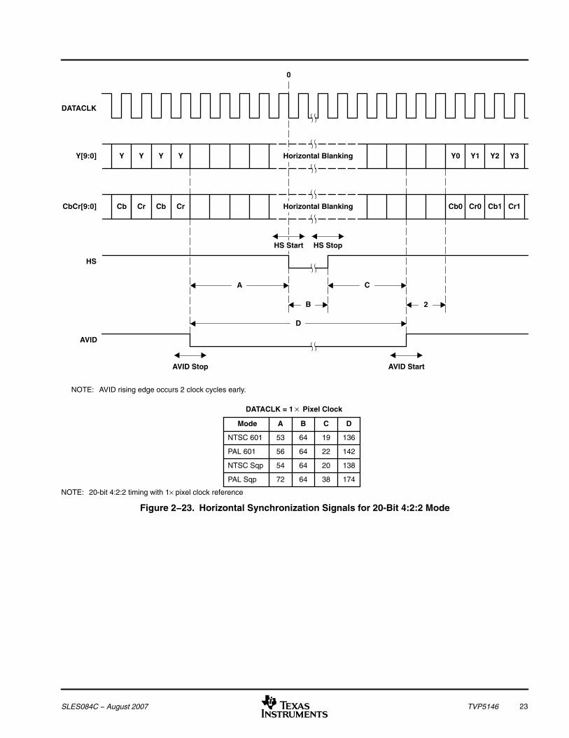
23SLES084C − August 2007 TVP5146
54
72
64
64
20
38
138
174
22
53 64 19
56
CbCr[9:0]
NTSC 601
PAL 601
DATACLK = 1 Pixel Clock
NTSC Sqp
PAL Sqp
64
Mode A B C
136
142
D
Cb
DATACLK
Cr Cb Cr Cb0 Cr0 Cb1 Cr1
0
HS Start
Horizontal Blanking
HS
HS Stop
A C
B
AVID
D
NOTE: AVID rising edge occurs 2 clock cycles early.
Y[9:0] Y Y Y Y Y0 Y1 Y2 Y3Horizontal Blanking
2
AVID Stop AVID Start
NOTE: 20-bit 4:2:2 timing with 1× pixel clock reference
Figure 2−23. Horizontal Synchronization Signals for 20-Bit 4:2:2 Mode

24 SLES084C − August 2007TVP5146
NTSC 601 64
PAL 601
10-Bit (PCLK = 2 Pixel Clock)
NTSC Sqp
PAL Sqp
64
64
64
ModeB/2
First Field B/2
858
864
780
944
H/2
32
20-Bit (PCLK = 1 Pixel Clock)
32
32
32
B/2
429
432
390
472
H/2
HS
VS
Second Field
HS
VS
B/2
H/2 + B/2 H/2 + B/2
Figure 2−24. VSYNC Position With Respect to HSYNC
2.5.3 Embedded SyncsStandards with embedded syncs insert the SAV and EAV codes into the data stream on therising and falling edges of AVID. These codes contain the V and F bits which also define verticaltiming. Table 2−3 gives the format of the SAV and EAV codes.
H equals 1 always indicates EAV. H equals 0 always indicates SAV. The alignment of V and F tothe line and field counter varies depending on the standard.
The P bits are protection bits:
P3 = V xor H; P2 = F xor H; P1 = F xor V; P0 = F xor V xor H
Table 2−3. EAV and SAV Sequence
D9 (MSB) D8 D7 D6 D5 D4 D3 D2 D1 D0
Preamble 1 1 1 1 1 1 1 1 1 1
Preamble 0 0 0 0 0 0 0 0 0 0
Preamble 0 0 0 0 0 0 0 0 0 0
Status word 1 F V H P3 P2 P1 P0 0 0
2.6 I2C Host InterfaceCommunication with the TVP5146 decoder is via an I2C host interface. The I2C standardconsists of two signals, the serial input/output data (SDA) line and the serial input clock line(SCL), which carry information between the devices connected to the bus. A third signal (I2CA)is used for slave address selection. Although an I2C system can be multimastered, the TVP5146decoder functions as a slave device only.

25SLES084C − August 2007 TVP5146
Because SDA and SCL are kept open-drain at a logic-high output level or when the bus is notdriven, the user must connect SDA and SCL to a positive supply voltage via a pullup resistor onthe board. The slave-address select signal, terminal 37 (I2CA), enables the use of two TVP5146decoders tied to the same I2C bus by controlling the least significant bit of the I2C deviceaddress.
Table 2−4. I2C Host Interface Terminal Description
SIGNAL TYPE DESCRIPTION
I2CA I Slave address selection
SCL I Input clock line
SDA I/O Input/output data line
2.6.1 Reset and I2C Bus Address Selection
The TVP5146 decoder can respond to two possible chip addresses. The address selection ismade at reset by an externally supplied level on the I2CA terminal. The TVP5146 decodersamples the level of terminal 37 at power up or at the trailing edge of RESETB and configuresthe I2C bus address bit A0. The I2CA terminal has an internal pulldown resistor to pull theterminal low to set a zero.
Table 2−5. I2C Address Selection
A6 A5 A4 A3 A2 A1 A0 (I2CA) R/W HEX
1 0 1 1 1 0 0 (default) 1/0 B9/B8
1 0 1 1 1 0 1 † 1/0 BB/BA† If terminal 37 is strapped to DVDD via a 2.2-kΩ resistor, I2C device address A0 is set to 1.
2.6.2 I2C Operation
S 1011 1000 ACK Subaddress ACK Send data ACK P
Data transfers occur using the following illustrated formats.
Read from I2C control registers
S 1011 1000 ACK Subaddress ACK S 1011 1001 ACK Receive data NAK P
S = I2C bus start conditionP = I2C bus stop conditionACK = Acknowledge generated by the slaveNAK = Acknowledge generated by the master, for multiple-byte read master with ACK for each byte except last byteSubaddrress = Subaddress byteData = Data byte, if more than one byte of data is transmitted (read and write), the subaddress pointer is automatically incremented.I2C bus address = Example showing that I2CA is in default mode. Write (B8h), read (B9h)
2.6.3 VBUS Access
The TVP5146 decoder has additional internal registers accessible through an indirect access toan internal 24-bit address wide VBUS. Figure 2−25 shows the VBUS registers access.

26 SLES084C − August 2007TVP5146
Single Byte
B8S ACK E8 ACK VA0 ACK VA1 ACK VA2 ACK P
VBUS Write
B8S ACK E0 ACK Send Data ACK P
Multiple Bytes
B8S ACK E8 ACK VA0 ACK VA1 ACK VA2 ACK P
B8S ACK E1 ACK Send Data ACK ACK PSend Data• • •
Single Byte
B8S ACK E8 ACK VA0 ACK VA1 ACK VA2 ACK P
VBUS Read
B8S ACK E0 ACK ACK
Multiple Bytes
B8S ACK E8 ACK VA0 ACK VA1 ACK VA2 ACK P
B8S ACK E1 ACK ACK NAK PRead Data• • •
Read Data NAK PS B9
S B9 ACK Read Data
HOSTProcessor I2C
VBUSData
I2C Registers
00h
E0h
E1h
VBUSAddress
E8h
EAh
FFh
VBUS[23:0]
LineMode
VBUS Registers
00 0000h
FIFO
VPS
VITC
WSS
CC 80 051Ch
80 0520h
80 052Ch
80 0600h
80 0700h
90 1904h
FF FFFFh
NOTE: Examples use default I2C address.ACK = Acknowledge generated by the slaveNAK = No Acknowledge generated by the master
Figure 2−25. VBUS Access

27SLES084C − August 2007 TVP5146
2.6.4 I2C Timing Requirements
The TVP5146 decoder requires delays in the I2C accesses to accommodate the internalprocessor timing. In accordance with I2C specifications, the TVP5146 decoder holds the I2Cclock line (SCL) low to indicate the wait period to the I2C master. If the I2C master is notdesigned to check for the I2C clock line held-low condition, then the maximum delays mustalways be inserted where required. These delays are of variable length; maximum delays areindicated in the following diagram:
Normal register
S 1011 1000 ACK Subaddress ACK Send data ACK Wait 64 µs P
2.7 VBI Data Processor
The TVP5146 VBI data processor (VDP) slices various data services like teletext (WST,NABTS), closed caption (CC), wide screen signaling (WSS), program delivery control (PDC),vertical interval time code (VITC), video program system (VPS), copy generation managementsystem (CGMS) data, and electronic program guide (Gemstar) 1x/2x. Table 2−6 shows thesupported VBI system.
These services are acquired by programming the VDP to enable the reception of one or moreVBI data standard(s) in the VBI. The VDP can be programmed on a line-per-line basis to enablesimultaneous reception of different VBI formats, one per line. The results are stored in a FIFOand/or registers. Because of its high data bandwidth, the teletext results are stored in FIFO only.The TVP5146 decoder provides fully decoded V-CHIP data to the dedicated registers atsubaddresses 800540h–800543h (see Sections 2.12.4 through 2.12.7).
Table 2−6. Supported VBI Systems
VBI SYSTEM STANDARD LINE NUMBER NUMBER OF BYTES
Teletext WST A SECAM 6–23 (Fields 1 and 2) 38
Teletext WST B PAL 6–22 (Fields 1 and 2) 43
Teletext NABTS C NTSC 10–21 (Fields 1 and 2) 34
Teletext NABTS D NTSC-J 10–21 (Fields 1 and 2) 35
Closed caption PAL 22 (Fields 1 and 2) 2
Closed caption NTSC 21 (Fields 1 and 2) 2
WSS PAL 23 (Fields 1 and 2) 14 bits
WSS-CGMS NTSC 20 (Fields 1 and 2) 20 bits
VITC PAL 6–22 9
VITC NTSC 10–20 9
VPS (PDC) PAL 16 13
V-CHIP (decoded) NTSC 21 (Field 2) 2
Gemstar 1× NTSC 2
Gemstar 2× NTSC 5 with frame byte
User Any Programmable Programmable
28 SLES084C − August 2007TVP5146
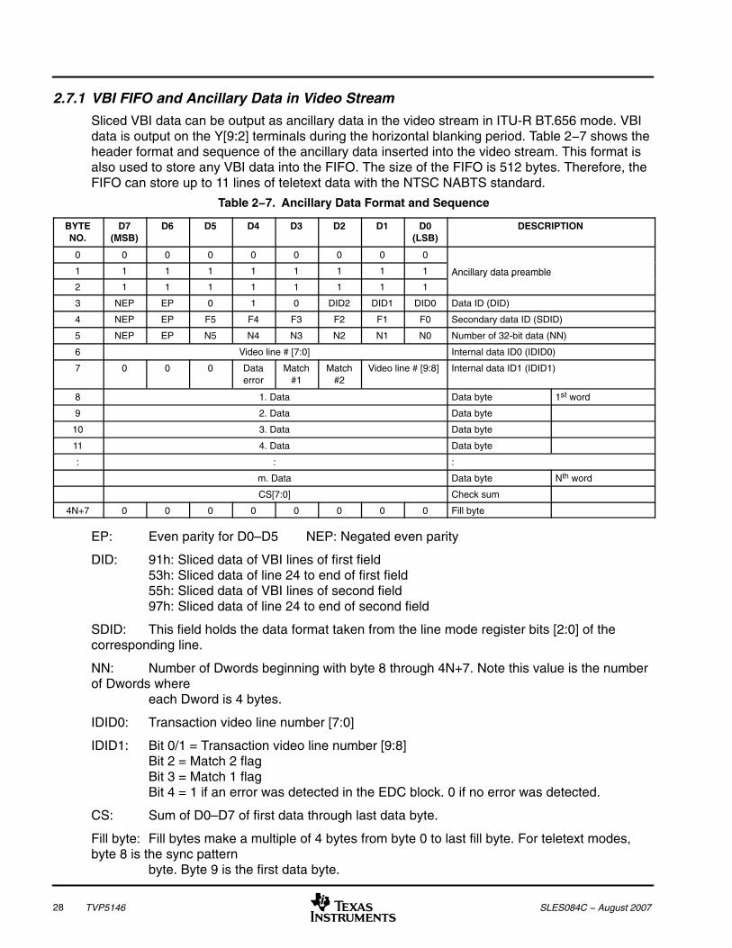
2.7.1 VBI FIFO and Ancillary Data in Video Stream
Sliced VBI data can be output as ancillary data in the video stream in ITU-R BT.656 mode. VBIdata is output on the Y[9:2] terminals during the horizontal blanking period. Table 2−7 shows theheader format and sequence of the ancillary data inserted into the video stream. This format isalso used to store any VBI data into the FIFO. The size of the FIFO is 512 bytes. Therefore, theFIFO can store up to 11 lines of teletext data with the NTSC NABTS standard.
Table 2−7. Ancillary Data Format and Sequence
BYTENO.
D7(MSB)
D6 D5 D4 D3 D2 D1 D0(LSB)
DESCRIPTION
0 0 0 0 0 0 0 0 0
1 1 1 1 1 1 1 1 1 Ancillary data preamble
2 1 1 1 1 1 1 1 1
Ancillary data preamble
3 NEP EP 0 1 0 DID2 DID1 DID0 Data ID (DID)
4 NEP EP F5 F4 F3 F2 F1 F0 Secondary data ID (SDID)
5 NEP EP N5 N4 N3 N2 N1 N0 Number of 32-bit data (NN)
6 Video line # [7:0] Internal data ID0 (IDID0)
7 0 0 0 Dataerror
Match#1
Match#2
Video line # [9:8] Internal data ID1 (IDID1)
8 1. Data Data byte 1st word
9 2. Data Data byte
10 3. Data Data byte
11 4. Data Data byte
: : :
m. Data Data byte Nth word
CS[7:0] Check sum
4N+7 0 0 0 0 0 0 0 0 Fill byte
EP: Even parity for D0–D5 NEP: Negated even parity
DID: 91h: Sliced data of VBI lines of first field53h: Sliced data of line 24 to end of first field55h: Sliced data of VBI lines of second field97h: Sliced data of line 24 to end of second field
SDID: This field holds the data format taken from the line mode register bits [2:0] of thecorresponding line.
NN: Number of Dwords beginning with byte 8 through 4N+7. Note this value is the numberof Dwords where
each Dword is 4 bytes.
IDID0: Transaction video line number [7:0]
IDID1: Bit 0/1 = Transaction video line number [9:8]Bit 2 = Match 2 flagBit 3 = Match 1 flagBit 4 = 1 if an error was detected in the EDC block. 0 if no error was detected.
CS: Sum of D0–D7 of first data through last data byte.
Fill byte: Fill bytes make a multiple of 4 bytes from byte 0 to last fill byte. For teletext modes,byte 8 is the sync pattern
byte. Byte 9 is the first data byte.

29SLES084C − August 2007 TVP5146
2.7.2 VBI Raw Data Output
The TVP5146 decoder can output raw A/D video data at twice the sampling rate for external VBIslicing. This is transmitted as an ancillary data block, although somewhat differently from theway the sliced VBI data is transmitted in the FIFO format as described in Section 2.7.1. Thesamples are transmitted during the active portion of the line. VBI raw data uses ITU-R BT.656format having only luma data. The chroma samples are replaced by luma samples. TheTVP5146 decoder inserts a four-byte preamble 000h 3FFh 3FFh 180h before data start. Thereare no checksum bytes and fill bytes in this mode.
Table 2−8. VBI Raw Data Output Format
BYTENO.
D9(MSB)
D8 D7 D6 D5 D4 D3 D2 D1 D0(LSB)
DESCRIPTION
0 0 0 0 0 0 0 0 0 0 0
1 1 1 1 1 1 1 1 1 1 1VBI raw data preamble
2 1 1 1 1 1 1 1 1 1 1VBI raw data preamble
3 0 1 1 0 0 0 0 0 0 0
4 1. Data
5 2. Data2 i l t l d t
: :2× pixel rate luma data(i e NTSC 601: n = 1707)
n–1 n–5. Data(i.e., NTSC 601: n = 1707)
n n–4. Data
2.8 Reset and Initialization
Reset is initiated at power up or any time terminal 34 (RESETB) is brought low. Table 2−9describes the status of the TVP5146 terminals during and immediately after reset.
Table 2−9. Reset Sequence
SIGNAL NAME DURING RESET RESET COMPLETED
Y[9:0], C[9:0], DATACLK Input High-impedance
RESETB, PWDN, SDA, SCL, FSS,AVID, GLCO, HS, VS, FID
Input Input
INTREQ Input Output
DATACLK Output High-impedance
TI recommends the following power-up sequence.
3 ms (min)
RESETB(Terminal 34)
1 ms (min)
Invalid I2C Cycle Valid
Normal Operation
100 s
SDA(Terminal 29)
Power (1.8 V)
Power (3.3 V)
Reset
NOTE: All times shown are minimum values. Maximum time between 1.8 V and 3.3 V should be no longer than 1 second.
Figure 2−26. Reset Timing

30 SLES084C − August 2007TVP5146
The TVP5146 requires that terminal 69 (C_1/GPIO) be held LOW. If using the 20-/16-bit modeor using this terminal as GPIO, then this terminal must be pulled low through a 2.2-kΩ pulldownresistor (see Figure 5−1). If unused, this terminal can be shorted to ground. (Note: If using the20-/16-bit mode and only using the 16 MSBs, it is possible to short terminal 69 to GND, but thecurrent for IOVDD will increase by 2 or 3 mA.)
After reset, the user must write the following I2C commands to the TVP5146:
STEP I2C SUBADDRESS I2C DATA
1 0xE8 0x02
2 0xE9 0x00
3 0xEA 0x80
4 0xE0 0x01
5 0xE8 0x60
6 0xE9 0x00
7 0xEA 0xB0
8 0xE0 0x01
9 0xE0 0x00
10 0x03 0x01
11 0x03 0x00
Afterward, the user programs the device as usual.
2.9 Adjusting External Syncs
The proper sequence to program the following external syncs is:
• To set NTSC, PAL-M, NTSC 443, PAL60 (525-line modes):
− Set the video standard to NTSC (register 02h)
− Set HSYNC, VSYNC, VBLK, and AVID external syncs (registers 16h through 24h)
• To set PAL, PAL-N, SECAM (625-line modes):
− Set the video standard to PAL (register 02h)
− Set HSYNC, VSYNC, VBLK, and AVID external syncs (registers 16h through 24h)
• For autoswitch, set the video standard to autoswitch (register 02h)
2.10 Internal Control Registers
The TVP5146 decoder is initialized and controlled by a set of internal registers that define theoperating parameters of the entire decoder. Communication between the external controller andthe TVP5146 decoder is through a standard I2C host port interface, as described earlier.Table 2−10 shows the summary of these registers. Detailed programming information for eachregister is described in the following sections. Additional registers are accessible through anindirect procedure involving access to an internal 24-bit address wide VBUS. Table 2−11 showsthe summary of the VBUS registers.
NOTE: Do not write to reserved registers. Reserved bits in any defined register must be writtenwith 0s, unless otherwise noted.

31SLES084C − August 2007 TVP5146
Table 2−10. Register Summary
REGISTER NAME I2C SUBADDRESS DEFAULT R/W
Input select 00h 00h R/W
AFE gain control 01h 0Fh R/W
Video standard 02h 00h R/W
Operation mode 03h 00h R/W
Autoswitch mask 04h 23h R/W
Color killer 05h 10h R/W
Luminance processing control 1 06h 00h R/W
Luminance processing control 2 07h 00h R/W
Luminance processing control 3 08h 02h R/W
Luminance brightness 09h 80h R/W
Luminance contrast 0Ah 80h R/W
Chrominance saturation 0Bh 80h R/W
Chroma hue 0Ch 00h R/W
Chrominance processing control 1 0Dh 00h R/W
Chrominance processing control 2 0Eh 0Eh R/W
Reserved 0Fh
Component Pr saturation 10h 80h R/W
Component Y contrast 11h 80h R/W
Component Pb saturation 12h 80h R/W
Reserved 13h
Component Y brightness 14h 80h R/W
Reserved 15h
AVID start pixel 16h–17h 055h R/W
AVID stop pixel 18h–19h 325h R/W
HSYNC start pixel 1Ah–1Bh 000h R/W
HSYNC stop pixel 1Ch–1Dh 040h R/W
VSYNC start line 1Eh–1Fh 004h R/W
VSYNC stop line 20h–21h 007h R/W
VBLK start line 22h–23h 001h R/W
VBLK stop line 24h–25h 015h R/W
NOTE: R = Read onlyW = Write onlyR/W = Read and writeReserved register addresses must not be written to.

32 SLES084C − August 2007TVP5146
Table 2−10. Registers Summary (Continued)
REGISTER NAME I2C SUBADDRESS DEFAULT R/W
Reserved 26h–27h
Fast-switch control 28h CCh R/W
Reserved 29h
Fast-switch SCART delay 2Ah 00h R/W
Reserved 2Bh
SCART delay 2Ch 00h R/W
CTI delay 2Dh 00h R/W
CTI control 2Eh 00h R/W
Reserved 2Fh–30h
RTC 31h 05h R/W
Sync control 32h 00h R/W
Output formatter 1 33h 40h R/W
Output formatter 2 34h 00h R/W
Output formatter 3 35h FFh R/W
Output formatter 4 36h FFh R/W
Output formatter 5 37h FFh R/W
Output formatter 6 38h FFh R/W
Clear lost lock detect 39h 00h R/W
Status 1 3Ah R
Status 2 3Bh R
AGC gain status 3Ch–3Dh R
Reserved 3Eh
Video standard status 3Fh R
GPIO input 1 40h R
GPIO input 2 41h R
Vertical line count 42h–43h R
Reserved 44h–45h R
AFE coarse gain for CH1 46h 20h R/W
AFE coarse gain for CH2 47h 20h R/W
AFE coarse gain for CH3 48h 20h R/W
AFE coarse gain for CH4 49h 20h R/W
AFE fine gain for Pb_B 4Ah–4Bh 900h R/W
AFE fine gain for Y_G_Chroma 4Ch–4Dh 900h R/W
AFE fine gain for Pr_R 4Eh–4Fh 900h R/W
AFE fine gain for CVBS_Luma 50h–51h 900h R/W
Reserved 52h–6Fh
ROM version 70h R
Reserved 71h–73h
AGC white peak processing 74h 00h R/W
Reserved 75h–77h
NOTE: R = Read onlyW = Write onlyR/W = Read and writeReserved register addresses must not be written to.
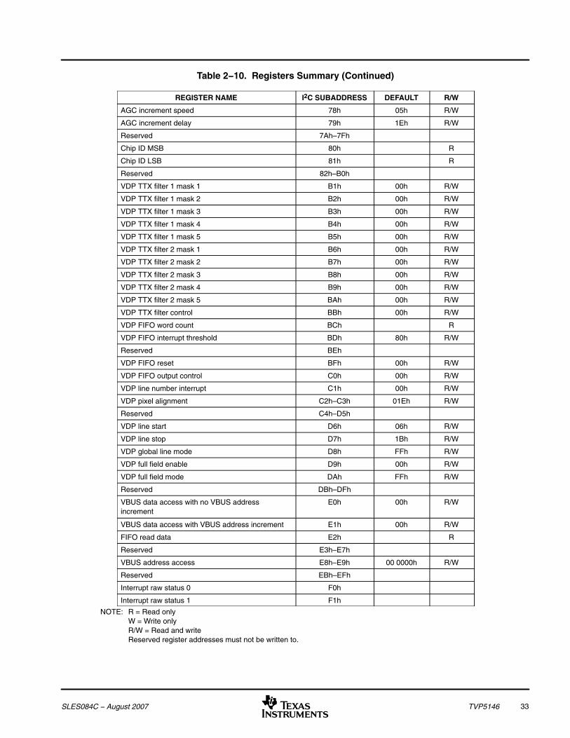
33SLES084C − August 2007 TVP5146
Table 2−10. Registers Summary (Continued)
REGISTER NAME I2C SUBADDRESS DEFAULT R/W
AGC increment speed 78h 05h R/W
AGC increment delay 79h 1Eh R/W
Reserved 7Ah–7Fh
Chip ID MSB 80h R
Chip ID LSB 81h R
Reserved 82h–B0h
VDP TTX filter 1 mask 1 B1h 00h R/W
VDP TTX filter 1 mask 2 B2h 00h R/W
VDP TTX filter 1 mask 3 B3h 00h R/W
VDP TTX filter 1 mask 4 B4h 00h R/W
VDP TTX filter 1 mask 5 B5h 00h R/W
VDP TTX filter 2 mask 1 B6h 00h R/W
VDP TTX filter 2 mask 2 B7h 00h R/W
VDP TTX filter 2 mask 3 B8h 00h R/W
VDP TTX filter 2 mask 4 B9h 00h R/W
VDP TTX filter 2 mask 5 BAh 00h R/W
VDP TTX filter control BBh 00h R/W
VDP FIFO word count BCh R
VDP FIFO interrupt threshold BDh 80h R/W
Reserved BEh
VDP FIFO reset BFh 00h R/W
VDP FIFO output control C0h 00h R/W
VDP line number interrupt C1h 00h R/W
VDP pixel alignment C2h–C3h 01Eh R/W
Reserved C4h–D5h
VDP line start D6h 06h R/W
VDP line stop D7h 1Bh R/W
VDP global line mode D8h FFh R/W
VDP full field enable D9h 00h R/W
VDP full field mode DAh FFh R/W
Reserved DBh–DFh
VBUS data access with no VBUS addressincrement
E0h 00h R/W
VBUS data access with VBUS address increment E1h 00h R/W
FIFO read data E2h R
Reserved E3h–E7h
VBUS address access E8h–E9h 00 0000h R/W
Reserved EBh–EFh
Interrupt raw status 0 F0h
Interrupt raw status 1 F1h
NOTE: R = Read onlyW = Write onlyR/W = Read and writeReserved register addresses must not be written to.

34 SLES084C − August 2007TVP5146
Table 2−10. Registers Summary (Continued)
REGISTER NAME I2C SUBADDRESS DEFAULT R/W
Interrupt status 0 F2h R/W
Interrupt status 1 F3h R/W
Interrupt mask 0 F4h 00h R/W
Interrupt mask 1 F5h 00h R/W
Interrupt clear 0 F6h 00h R/W
Interrupt clear 1 F7h 00h R/W
Reserved F8h–FFh
NOTE: R = Read onlyW = Write onlyR/W = Read and writeReserved register addresses must not be written to.
Table 2−11. VBUS Register Summary
REGISTER NAME I2C SUBADDRESS DEFAULT R/W
Reserved 00 0000h–80 051Bh
VDP closed caption data 80 051Ch–80 051Fh R
VDP WSS data 80 0520h–80 0526h R
Reserved 80 0527h–80 052Bh
VDP VITC data 80 052Ch–80 0534h R
Reserved 80 0535h–80 053Fh
VDP V-Chip data 80 0540h–80 0543h R
Reserved 80 0544h–80 05FFh
VDP general line mode and line address 80 0600h–80 0611h 00h, FFh R/W
Reserved 80 0612h–80 06FFh
VDP VPS/Gemstar data 80 0700h–80 070Ch R
Reserved 80 070Dh–90 1903h
VDP FIFO read 90 1904h R
Reserved 90 1905h–B0 005Fh
Interrupt configuration B0 0060h 00h R/W
Reserved B0 0061h–FF FFFFh
NOTE: Writing any value to a reserved register may cause erroneous operation of the TVP5146 decoder.It is recommended not to access any data to/from reserved registers.

35SLES084C − August 2007 TVP5146
2.11 Register Definitions
2.11.1 Input Select RegisterSubaddress 00h
Default 00h
7 6 5 4 3 2 1 0
Input select [7:0]
Table 2−12. Analog Channel and Video Mode Selection
MODE INPUT(S) SELECTEDINPUT SELECT [7:0]
MODE INPUT(S) SELECTED7 6 5 4 3 2 1 0 HEX
CVBS VI_1_A (default) 0 0 0 0 0 0 0 0 00
VI_1_B 0 0 0 0 0 0 0 1 01
VI_1_C 0 0 0 0 0 0 1 0 02
VI_2_A 0 0 0 0 0 1 0 0 04
VI_2_B 0 0 0 0 0 1 0 1 05
VI_2_C 0 0 0 0 0 1 1 0 06
VI_3_A 0 0 0 0 1 0 0 0 08
VI_3_B 0 0 0 0 1 0 0 1 09
VI_3_C 0 0 0 0 1 0 1 0 0A
VI_4_A 0 0 0 0 1 1 0 0 0C
S-video VI_2_A(Y), VI_1_A(C) 0 1 0 0 0 1 0 0 44
VI_2_B(Y), VI_1_B(C) 0 1 0 0 0 1 0 1 45
VI_2_C(Y), VI_1_C(C) 0 1 0 0 0 1 1 0 46
VI_2_A(Y), VI_3_A(C) 0 1 0 1 0 1 0 0 54
VI_2_B(Y), VI_3_B(C) 0 1 0 1 0 1 0 1 55
VI_2_C(Y), VI_3_C(C) 0 1 0 1 0 1 1 0 56
VI_4_A(Y), VI_1_A(C) 0 1 0 0 1 1 0 0 4C
VI_4_A(Y), VI_1_B(C) 0 1 0 0 1 1 0 1 4D
VI_4_A(Y), VI_1_C(C) 0 1 0 0 1 1 1 0 4E
VI_4_A(Y), VI_3_A(C) 0 1 0 1 1 1 0 0 5C
VI_4_A(Y), VI_3_B(C) 0 1 0 1 1 1 0 1 5D
VI_4_A(Y), VI_3_C(C) 0 1 0 1 1 1 1 0 5E
RGB VI_1_A(B), VI_2_A(G), VI_3_A(R) 1 0 0 0 0 1 0 0 84
VI_1_B(B), VI_2_B(G), VI_3_B(R) 1 0 0 0 0 1 0 1 85
VI_1_C(B), VI_2_C(G), VI_3_C(R) 1 0 0 0 0 1 1 0 86
YPbPr VI_1_A(Pb), VI_2_A(Y), VI_3_A(Pr) 1 0 0 1 0 1 0 0 94
VI_1_B(Pb), VI_2_B(Y), VI_3_B(Pr) 1 0 0 1 0 1 0 1 95
VI_1_C(Pb), VI_2_C(Y), VI_3_C(Pr) 1 0 0 1 0 1 1 0 96
SCART VI_1_A(B), VI_2_A(G), VI_3_A(R), VI_4_A(CVBS) 1 1 0 0 1 1 0 0 CC
VI_1_B(B), VI_2_B(G), VI_3_B(R), VI_4_A(CVBS) 1 1 0 0 1 1 0 1 CD
VI_1_C(B), VI_2_C(G), VI_3_C(R), VI_4_A(CVBS) 1 1 0 0 1 1 1 0 CE
VI_1_A(Pb), VI_2_A(Y), VI_3_A(Pr), VI_4_A(CVBS) 1 1 0 1 1 1 0 0 DC
VI_1_B(Pb), VI_2_B(Y), VI_3_B(Pr), VI_4_A(CVBS) 1 1 0 1 1 1 0 1 DD
VI_1_C(Pb), VI_2_C(Y), VI_3_C(Pr), VI_4_A(CVBS) 1 1 0 1 1 1 1 0 DE
Ten input terminals can be configured to support composite, S-video, and componentYPbPr/RGB or SCART as listed in Table 2−12. Users must follow this table properly for S-videoand component applications because only the terminal configurations listed in Table 2−12 aresupported.

36 SLES084C − August 2007TVP5146
2.11.2 AFE Gain Control RegisterSubaddress 01h
Default 0Fh
7 6 5 4 3 2 1 0
Reserved 1 1 AGC chroma AGC luma
Bit 3: 1 must be written to this bit.
Bit 2: 1 must be written to this bit.
AGC chroma: Controls automatic gain in the chroma/B/R/PbPr channel:
0 = Manual (if AGC luma is set to manual, AGC chroma is forced to be in manual)1 = Enabled auto gain, applies a gain value acquired from the sync channel for S-video and component
mode. When AGC luma is set, this state is valid. (default)
AGC luma: Controls automatic gain in the embedded sync channel of CVBS, S-video,component video:
0 = Manual gain, AFE coarse and fine gain frozen to the previous gain value set by a AGC when this bit isset to 0.1 = Enabled auto gain applies only to the embedded sync channel (default)
These settings only affect the analog front-end (AFE). The brightness and contrast ofcomponent, CVBS are not affected by these settings.
2.11.3 Video Standard RegisterSubaddress 02h
Default 00h
7 6 5 4 3 2 1 0
Reserved Video standard [2:0]
Video standard [2:0]:
CVBS and S-Video Component Video000 = Autoswitch mode (default) Autoswitch mode (default)001 = (M, J) NTSC Component 525010 = (B, D, G, H, I, N) PAL Component 625011 = (M) PAL Reserved100 = (Combination-N) PAL Reserved101 = NTSC 4.43 Reserved110 = SECAM Reserved111 = PAL 60 Reserved
NOTE: PAL60 is not included in autoswitch mode.
With the autoswitch code running, the user can force the decoder to operate in a particular videostandard mode by writing the appropriate value into this register. Changing these bits causes theregister settings to be reinitialized.
NOTE: Sampling rate (either square pixel or ITU-R BT.601) can be set by bit 7 (sampling rate) in the outputformatter 1 register at I2C subaddress 33h (see Section 2.11.35).

37SLES084C − August 2007 TVP5146
2.11.4 Operation Mode RegisterSubaddress 03h
Default 00h
7 6 5 4 3 2 1 0
Reserved Power save
Power save:
0 = Normal operation (default) 1 = Power-save mode. Reduces the clock speed of the internal processor and switches off the ADCs. I2C
interface is active and all current operating settings are preserved.
2.11.5 Autoswitch Mask RegisterSubaddress 04h
Default 23h
7 6 5 4 3 2 1 0
Reserved SECAM NTSC 4.43 (Nc) PAL (M) PAL PAL (M, J) NTSC
Autoswitch mode mask: Limits the video formats between which autoswitch is possible.
SECAM:
0 = Autoswitch does not include SECAM1 = Autoswitch includes SECAM (default)
NTSC 4.43:
0 = Autoswitch does not include NTSC 4.43 (default)1 = Autoswitch includes NTSC 4.43
(Nc) PAL:
0 = Autoswitch does not include (Nc) PAL (default)1 = Autoswitch includes (Nc) PAL
(M) PAL:
0 = Autoswitch does not include (M) PAL (default)1 = Autoswitch includes (M) PAL
PAL:
0 = Reserved1 = Autoswitch includes (B, D, G, H, I, N) PAL (default)
(M, J ) NTSC:
0 = Reserved1 = Autoswitch includes (M, J) NTSC (default)
NOTE: Bits 1 and 0 must always be 1.

38 SLES084C − August 2007TVP5146
2.11.6 Color Killer RegisterSubaddress 05h
Default 10h
7 6 5 4 3 2 1 0
Reserved Automatic color killer Color killer threshold [4:0]
Automatic color killer:
00 = Automatic mode (default)01 = Reserved10 = Color killer enabled, the C terminals are forced to a zero color state.11 = Color killer disabled
Color killer threshold [4:0]:
1 1111 = 31 (maximum)1 0000 = 16 (default)0 0000 = 0 (minimum)
2.11.7 Luminance Processing Control 1 RegisterSubaddress 06h
Default 00h
7 6 5 4 3 2 1 0
Reserved Pedestal not present Reserved VBI raw Luminance signal delay [3:0]
Pedestal not present:
0 = 7.5 IRE pedestal is present on the analog video input signal (default)1 = Pedestal is not present on the analog video input signal
VBI raw:
0 = Disabled (default)1 = Enabled
During the duration of the vertical blanking as defined by the VBLK start and stop line registersat subaddresses 22h through 25h (see Sections 2.11.26 and 2.11.27), the chroma samples arereplaced by luma samples. This feature can be used to support VBI processing performed by anexternal device during the VBI. In order to use this bit, the output format must be 10-bit ITU-RBT.656 mode.
Luminance signal delay [3:0]: Luminance signal delays with respect to the chroma signal in 1×pixel clock increments.
0111 = Reserved0110 = 6-pixel delay0001 = 1-pixel delay0000 = 0 delay (default)1111 = –1-pixel delay1000 = –8-pixel delay
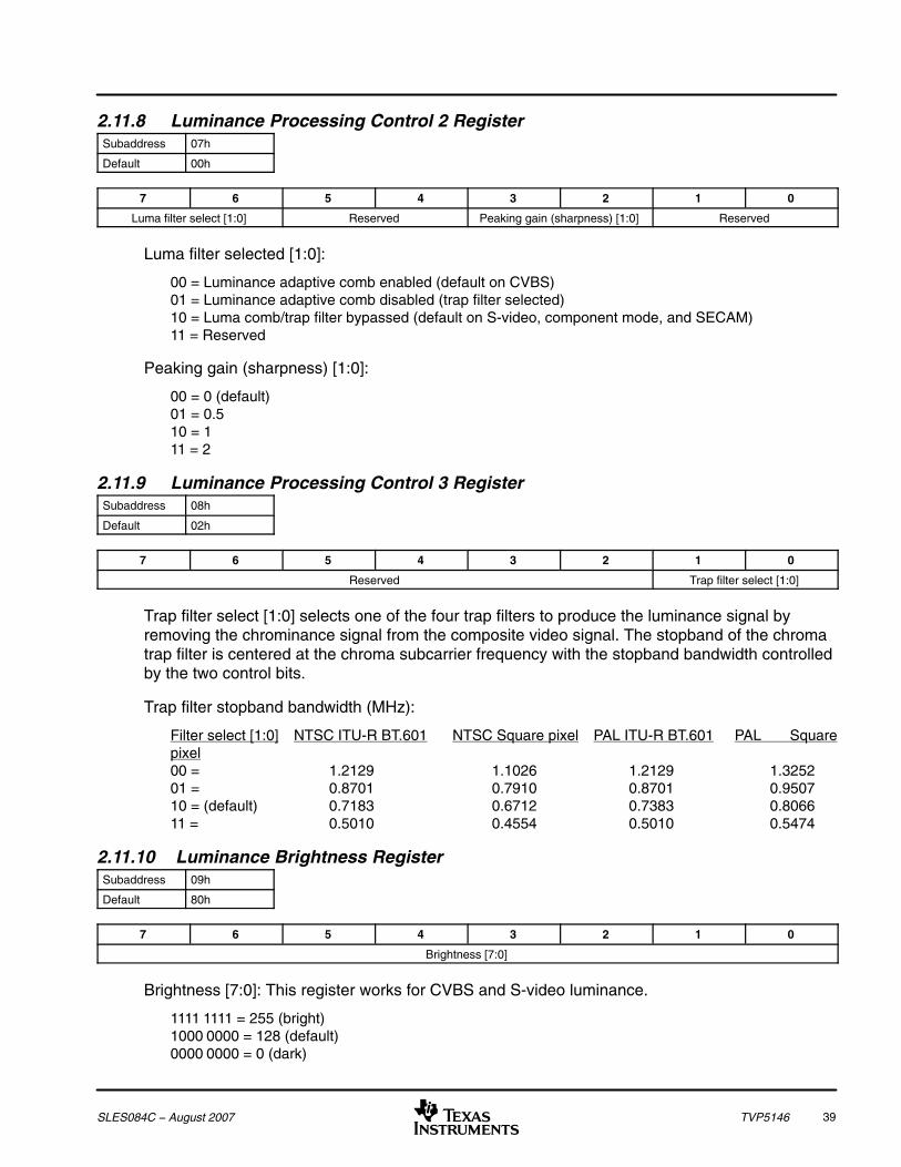
39SLES084C − August 2007 TVP5146
2.11.8 Luminance Processing Control 2 RegisterSubaddress 07h
Default 00h
7 6 5 4 3 2 1 0
Luma filter select [1:0] Reserved Peaking gain (sharpness) [1:0] Reserved
Luma filter selected [1:0]:
00 = Luminance adaptive comb enabled (default on CVBS)01 = Luminance adaptive comb disabled (trap filter selected)10 = Luma comb/trap filter bypassed (default on S-video, component mode, and SECAM)11 = Reserved
Peaking gain (sharpness) [1:0]:
00 = 0 (default)01 = 0.510 = 111 = 2
2.11.9 Luminance Processing Control 3 RegisterSubaddress 08h
Default 02h
7 6 5 4 3 2 1 0
Reserved Trap filter select [1:0]
Trap filter select [1:0] selects one of the four trap filters to produce the luminance signal byremoving the chrominance signal from the composite video signal. The stopband of the chromatrap filter is centered at the chroma subcarrier frequency with the stopband bandwidth controlledby the two control bits.
Trap filter stopband bandwidth (MHz):
Filter select [1:0] NTSC ITU-R BT.601 NTSC Square pixel PAL ITU-R BT.601 PAL Squarepixel 00 = 1.2129 1.1026 1.2129 1.325201 = 0.8701 0.7910 0.8701 0.950710 = (default) 0.7183 0.6712 0.7383 0.806611 = 0.5010 0.4554 0.5010 0.5474
2.11.10 Luminance Brightness RegisterSubaddress 09h
Default 80h
7 6 5 4 3 2 1 0
Brightness [7:0]
Brightness [7:0]: This register works for CVBS and S-video luminance.
1111 1111 = 255 (bright)1000 0000 = 128 (default)0000 0000 = 0 (dark)

40 SLES084C − August 2007TVP5146
2.11.11 Luminance Contrast RegisterSubaddress 0Ah
Default 80h
7 6 5 4 3 2 1 0
Contrast [7:0]
Contrast [7:0]: This register works for CVBS and S-video luminance.
1111 1111 = 255 (maximum contrast)1000 0000 = 128 (default)0000 0000 = 0 (minimum contrast)
2.11.12 Chrominance Saturation RegisterSubaddress 0Bh
Default 80h
7 6 5 4 3 2 1 0
Saturation [7:0]
Saturation [7:0]: This register works for CVBS and S-video chrominance.
1111 1111 = 255 (maximum)1000 0000 = 128 (default)0000 0000 = 0 (no color)
2.11.13 Chroma Hue RegisterSubaddress 0Ch
Default 00h
7 6 5 4 3 2 1 0
Hue [7:0]
Hue [7:0] (does not apply to a component video): This register works for CVBS and S-videochrominance.
0111 1111 = +180 degrees0000 0000 = 0 degrees (default)1000 0000 = –180 degrees

41SLES084C − August 2007 TVP5146
2.11.14 Chrominance Processing Control 1 RegisterSubaddress 0Dh
Default 00h
7 6 5 4 3 2 1 0
Reserved Color PLL resetChrominance adaptive
comb enableReserved Automatic color gain control [1:0]
Color PLL reset:
0 = Color subcarrier PLL not reset (default)1 = Color subcarrier PLL reset
Chrominance adaptive comb enable: This bit is effective on composite video only.
0 = Enabled (default)1 = Disabled
Automatic color gain control (ACGC) [1:0]:
00 = ACGC enabled (default)01 = Reserved10 = ACGC disabled, ACGC set to the nominal value11 = ACGC frozen to the previous set value
2.11.15 Chrominance Processing Control 2 RegisterSubaddress 0Eh
Default 0Eh
7 6 5 4 3 2 1 0
Reserved PAL compensation WCF Chrominance filter select [1:0]
PAL compensation:
0 = Disabled1 = Enabled (default)
WCF: Wideband chroma LPF filter
0 = Disabled1 = Enabled (default)
Chrominance filter select [1:0]:
00 = Disabled01 = Notch 110 = Notch 2 (default)11 = Notch 3See Figure 2−8 through Figure 2−11 for characteristics.
2.11.16 Component Pr Saturation RegisterSubaddress 10h
Default 80h
7 6 5 4 3 2 1 0
Pr saturation [7:0]
Pr saturation [7:0]: This register works only with YPbPr component video. For RGB video, usermust use the AFE gain registers.
1111 1111 = 255 (maximum)1000 0000 = 128 (default)0000 0000 = 0 (minimum)

42 SLES084C − August 2007TVP5146
2.11.17 Component Y Contrast RegisterSubaddress 11h
Default 80h
7 6 5 4 3 2 1 0
Y contrast [7:0]
Y contrast [7:0]: This register works only with YPbPr component video. For RGB video, usermust use the AFE gain registers.
1111 1111 = 255 (maximum)1000 0000 = 128 (default)0000 0000 = 0 (minimum)

43SLES084C − August 2007 TVP5146
2.11.18 Component Pb Saturation RegisterSubaddress 12h
Default 80h
7 6 5 4 3 2 1 0
Pb saturation [7:0]
Pb saturation [7:0]: This register works only with YPbPr component video. For RGB video, usermust use the AFE gain registers.
1111 1111 = 255 (maximum)1000 0000 =128 (default)0000 0000 = 0 (minimum)
2.11.19 Component Y Brightness RegisterSubaddress 14h
Default 80h
7 6 5 4 3 2 1 0
Y brightness [7:0]
Y brightness [7:0]: This register works only with YPbPr component video.
1111 1111 = 255 (maximum)1000 0000 = 128 (default)0000 0000 = 0 (minimum)
2.11.20 AVID Start Pixel RegisterSubaddress 16h–17h
Default 055h
Subaddress 7 6 5 4 3 2 1 0
16h AVID start [7:0]
17h Reserved AVID active Reserved AVID start [9:8]
AVID active:
0 = AVID out active in VBLK (default) 1 = AVID out inactive in VBLK
AVID start [9:0]: AVID start pixel number, this is a absolute pixel location from HSYNC start pixel0.
NTSC 601 NTSC Sqp PAL 601 PAL Sqp default 85 (55h) 86 (56h) 88 (58h) 103 (67h)
The TVP5146 decoder updates the AVID start only when the AVID start MSB byte is written to. Ifthe user changes these registers, then the TVP5146 decoder retains values in different modesuntil this decoder resets. The AVID start pixel register also controls the position of the SAV code.

44 SLES084C − August 2007TVP5146
2.11.21 AVID Stop Pixel RegisterSubaddress 18h–19h
Default 325h
Subaddress 7 6 5 4 3 2 1 0
18h AVID stop [7:0]
19h Reserved AVID stop [9:8]
AVID stop [9:0]: AVID stop pixel number. The number of pixels of active video must be an evennumber. This is an absolute pixel location from HSYNC start pixel 0.
NTSC 601 NTSC Sqp PAL 601 PAL Sqp default 805 (325h) 726 (2D6h) 808 (328h) 696 (2B8h)
The TVP5146 decoder updates the AVID stop only when the AVID stop MSB byte is written to. Ifthe user changes these registers, then the TVP5146 decoder retains values in different modesuntil this decoder resets. The AVID start pixel register also controls the position of the EAV code.
2.11.22 HSYNC Start Pixel RegisterSubaddress 1Ah–1Bh
Default 000h
Default (000h)
Subaddress 7 6 5 4 3 2 1 0
1Ah HSYNC start [7:0]
1Bh Reserved HSYNC start [9:8]
HSYNC start pixel [9:0]: This is an absolute pixel location from HSYNC start pixel 0.The TVP5146 decoder updates the HSYNC start only when the HSYNC start MSB byte iswritten to. If the user changes these registers, then the TVP5146 decoder retains values indifferent modes until this decoder resets.
2.11.23 HSYNC Stop Pixel RegisterSubaddress 1Ch–1Dh
Default 040h
Subaddress 7 6 5 4 3 2 1 0
1Ch HSYNC stop [7:0]
1Dh Reserved HSYNC stop [9:8]
HSYNC stop [9:0]: This is an absolute pixel location from HSYNC start pixel 0.The TVP5146 decoder updates the HSYNC stop only when the HSYNC Stop MSB byte iswritten to. If the user changes these registers, then the TVP5146 decoder retains values indifferent modes until this decoder resets.

45SLES084C − August 2007 TVP5146
2.11.24 VSYNC Start Line RegisterSubaddress 1Eh–1Fh
Default 004h
Subaddress 7 6 5 4 3 2 1 0
1Eh VSYNC start [7:0]
1Fh Reserved VSYNC start [9:8]
VSYNC start [9:0]: This is an absolute line number. The TVP5146 decoder updates the VSYNCstart only when the VSYNC start MSB byte is written to. If the user changes these registers, thenthe TVP5146 decoder retains values in different modes until this decoder resets.NTSC: default 004h, PAL: default 001h
2.11.25 VSYNC Stop Line RegisterSubaddress 20h–21h
Default 007h
Subaddress 7 6 5 4 3 2 1 0
20h VSYNC stop [7:0]
21h Reserved VSYNC stop [9:8]
VSYNC stop [9:0]: This is an absolute line number. The TVP5146 decoder updates the VSYNCstop only when the VSYNC stop MSB byte is written to. If the user changes these registers, theTVP5146 decoder retains values in different modes until this decoder resets.NTSC: default 007h, PAL: default 004h
2.11.26 VBLK Start Line RegisterSubaddress 22h–23h
Default 001h
Subaddress 7 6 5 4 3 2 1 0
22h VBLK start [7:0]
23h Reserved VBLK start [9:8]
VBLK start [9:0]: This is an absolute line number. The TVP5146 decoder updates the VBLK startline only when the VBLK start MSB byte is written to. If the user changes these registers, theTVP5146 decoder retains values in different modes until this decoder resets.NTSC: default 001h, PAL: default 623 (26Fh)
2.11.27 VBLK Stop Line RegisterSubaddress 24h–25h
Default 015h
Subaddress 7 6 5 4 3 2 1 0
24h VBLK stop [7:0]
25h Reserved VBLK stop [9:8]
VBLK stop [9:0]: This is an absolute line number. The TVP5146 decoder updates the VBLK stoponly when the VBLK stop MSB byte is written to. If the user changes these registers, then theTVP5146 decoder retains values in different modes until this decoder resets.NTSC: default 21 (15h), PAL: default 23 (17h)
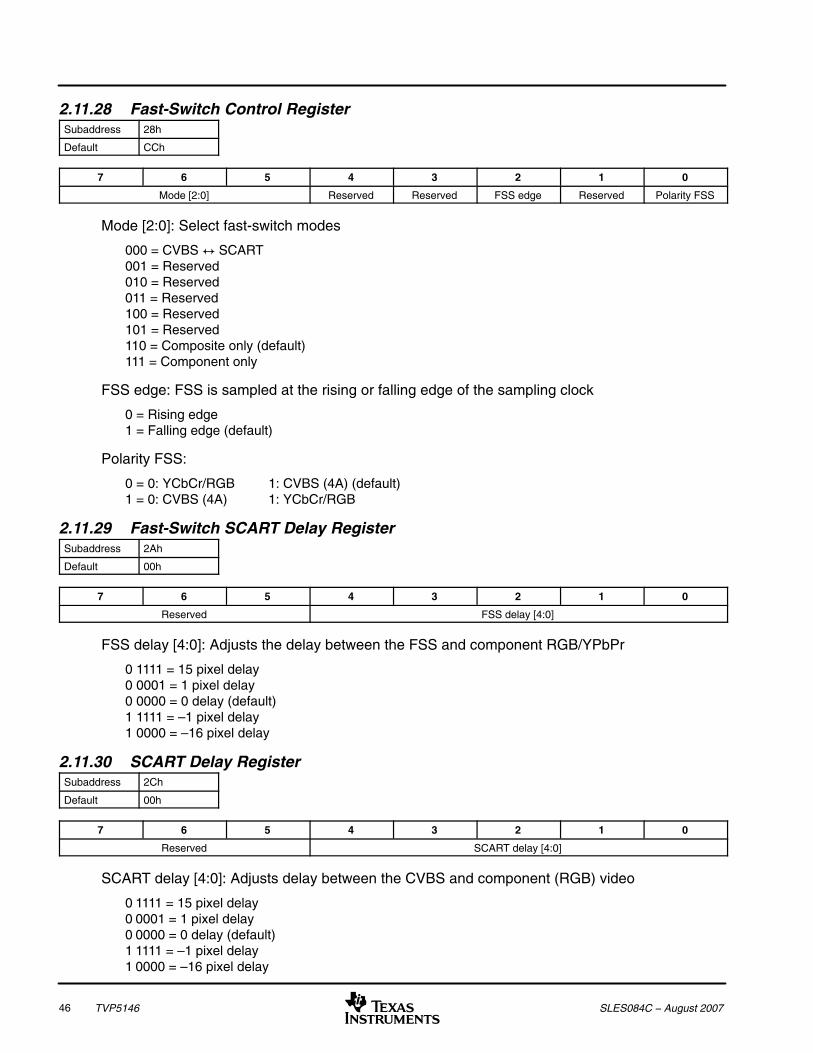
46 SLES084C − August 2007TVP5146
2.11.28 Fast-Switch Control RegisterSubaddress 28h
Default CCh
7 6 5 4 3 2 1 0
Mode [2:0] Reserved Reserved FSS edge Reserved Polarity FSS
Mode [2:0]: Select fast-switch modes
000 = CVBS SCART001 = Reserved010 = Reserved011 = Reserved100 = Reserved101 = Reserved110 = Composite only (default)111 = Component only
FSS edge: FSS is sampled at the rising or falling edge of the sampling clock
0 = Rising edge1 = Falling edge (default)
Polarity FSS:
0 = 0: YCbCr/RGB 1: CVBS (4A) (default)1 = 0: CVBS (4A) 1: YCbCr/RGB
2.11.29 Fast-Switch SCART Delay RegisterSubaddress 2Ah
Default 00h
7 6 5 4 3 2 1 0
Reserved FSS delay [4:0]
FSS delay [4:0]: Adjusts the delay between the FSS and component RGB/YPbPr
0 1111 = 15 pixel delay0 0001 = 1 pixel delay0 0000 = 0 delay (default)1 1111 = –1 pixel delay1 0000 = –16 pixel delay
2.11.30 SCART Delay RegisterSubaddress 2Ch
Default 00h
7 6 5 4 3 2 1 0
Reserved SCART delay [4:0]
SCART delay [4:0]: Adjusts delay between the CVBS and component (RGB) video
0 1111 = 15 pixel delay0 0001 = 1 pixel delay0 0000 = 0 delay (default)1 1111 = –1 pixel delay1 0000 = –16 pixel delay

47SLES084C − August 2007 TVP5146
2.11.31 CTI Delay RegisterSubaddress 2Dh
Default 00h
7 6 5 4 3 2 1 0
Reserved CTI delay [2:0]
CTI delay [2:0]: Sets the delay of the Y channel with respect to Cb/Cr in the CTI block
011 = 3 pixel delay001 = 1 pixel delay000 = 0 delay (default)111 = –1 pixel delay100 = –4 pixel delay
2.11.32 CTI Control RegisterSubaddress 2Eh
Default 00h
7 6 5 4 3 2 1 0
CTI coring [3:0] CTI gain [3:0]
CTI coring [3:0]: 4-bit CTI coring limit control value, unsigned linear control range from 0 to ±60,step size = 4
1111 = ±600001 = ±40000 = 0 (default)
CTI gain [3:0]: 4-bit CTI gain control values, unsigned linear control range from 0 to 15/16, stepsize = 1/16
1111 = 15/160001 = 1/160000 = 0 disabled (default)
2.11.33 RTC RegisterSubaddress 31h
Default 05h
7 6 5 4 3 2 1 0
Reserved Genlock [2:0]
Genlock [2:0]:
000 = Reserved001 = Reserved010 = Reserved011 = Reserved100 = Reserved101 = RTC mode110 = Reserved111 = Reserved

48 SLES084C − August 2007TVP5146
2.11.34 Sync Control RegisterSubaddress 32h
Default 00h
7 6 5 4 3 2 1 0
Reserved Polarity FID Polarity VS Polarity HS VS/VBLK HS/CS
Polarity FID: determines polarity of FID terminal
0 = First field high, second field low (default)1 = First field low, second field high
Polarity VS: determines polarity of VS terminal
0 = Active low (default)1 = Active high
Polarity HS: determines polarity of HS terminal
0 = Active low (default)1 = Active high
VS/VBLK:
0 = VS terminal outputs vertical sync (default)1 = VS terminal outputs vertical blank
HS/CS:
0 = HS terminal outputs horizontal sync (default)1 = HS terminal outputs composite sync
2.11.35 Output Formatter 1 RegisterSubaddress 33h
Default 40h
7 6 5 4 3 2 1 0
Sampling rate YCbCr code range CbCr code Reserved Output format [2:0]
Sampling rate (changing this bit causes the register settings to be reinitialized):
0 = ITU-R BT.601 sampling rate (default)1 = Square pixel sampling rate
YCbCr code range:
0 = ITU-R BT.601 coding range (Y ranges from 64 to 940. Cb and Cr range from 64 to 960.)1 = Extended coding range (Y, Cb, and Cr range from 4 to 1016) (default)
CbCr code:
0 = Offset binary code (2s complement + 512) (default)1 = Straight binary code (2s complement)
Output format [2:0]:
000 = 10-bit 4:2:2 (2× pixel rate) with embedded syncs (ITU-R BT.656) (default)001 = 20-bit 4:2:2 (pixel rate) with separate syncs010 = Reserved011 = 10-bit 4:2:2 with separate syncs100–111= Reserved
NOTE: 10-bit mode is also used for the raw VBI output mode when bit 4 (VBI raw) in theluminance processing control 1 register at subaddress 06h is set (see Section 2.11.7).
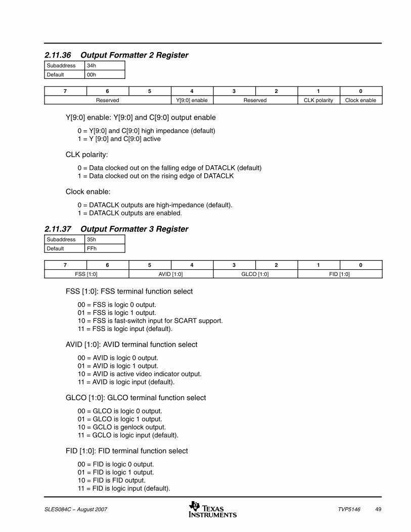
49SLES084C − August 2007 TVP5146
2.11.36 Output Formatter 2 RegisterSubaddress 34h
Default 00h
7 6 5 4 3 2 1 0
Reserved Y[9:0] enable Reserved CLK polarity Clock enable
Y[9:0] enable: Y[9:0] and C[9:0] output enable
0 = Y[9:0] and C[9:0] high impedance (default)1 = Y [9:0] and C[9:0] active
CLK polarity:
0 = Data clocked out on the falling edge of DATACLK (default)1 = Data clocked out on the rising edge of DATACLK
Clock enable:
0 = DATACLK outputs are high-impedance (default).1 = DATACLK outputs are enabled.
2.11.37 Output Formatter 3 RegisterSubaddress 35h
Default FFh
7 6 5 4 3 2 1 0
FSS [1:0] AVID [1:0] GLCO [1:0] FID [1:0]
FSS [1:0]: FSS terminal function select
00 = FSS is logic 0 output.01 = FSS is logic 1 output.10 = FSS is fast-switch input for SCART support.11 = FSS is logic input (default).
AVID [1:0]: AVID terminal function select
00 = AVID is logic 0 output.01 = AVID is logic 1 output.10 = AVID is active video indicator output.11 = AVID is logic input (default).
GLCO [1:0]: GLCO terminal function select
00 = GLCO is logic 0 output.01 = GLCO is logic 1 output.10 = GCLO is genlock output.11 = GCLO is logic input (default).
FID [1:0]: FID terminal function select
00 = FID is logic 0 output.01 = FID is logic 1 output.10 = FID is FID output.11 = FID is logic input (default).
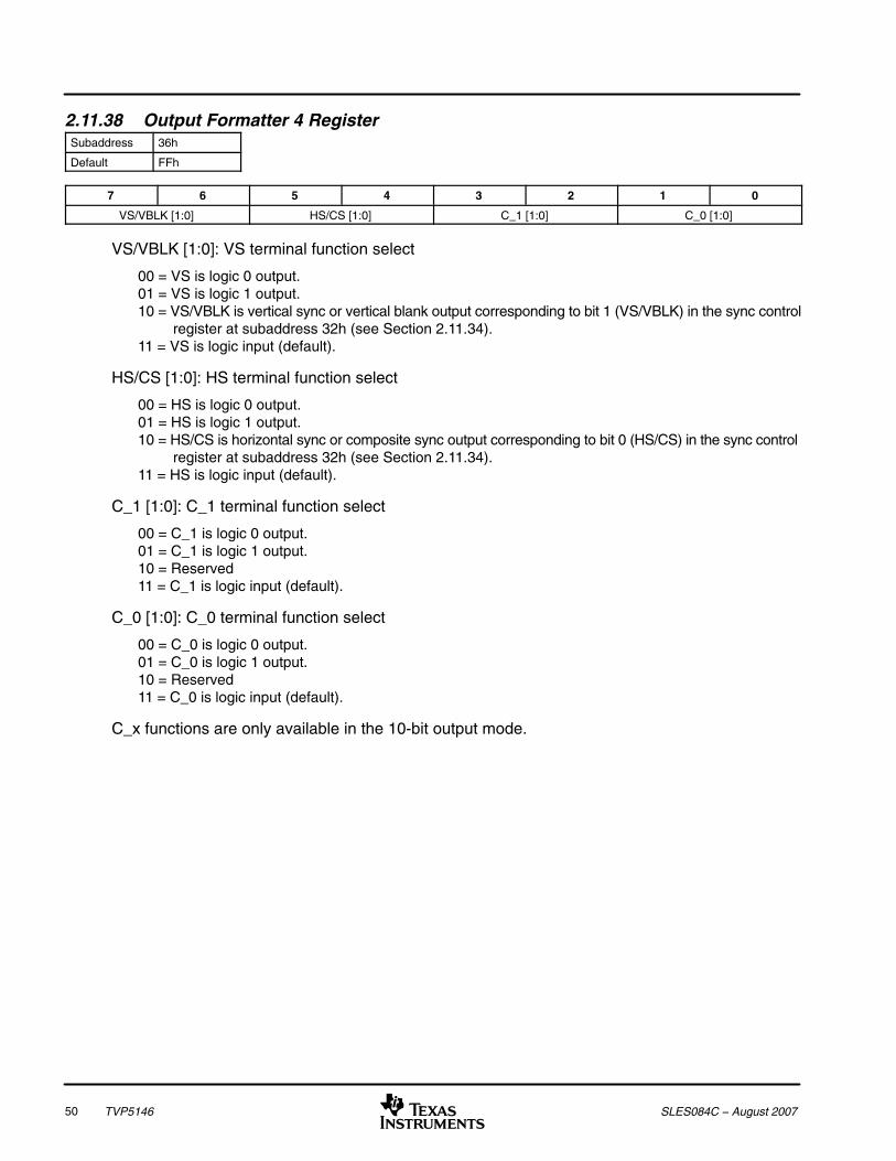
50 SLES084C − August 2007TVP5146
2.11.38 Output Formatter 4 RegisterSubaddress 36h
Default FFh
7 6 5 4 3 2 1 0
VS/VBLK [1:0] HS/CS [1:0] C_1 [1:0] C_0 [1:0]
VS/VBLK [1:0]: VS terminal function select
00 = VS is logic 0 output.01 = VS is logic 1 output.10 = VS/VBLK is vertical sync or vertical blank output corresponding to bit 1 (VS/VBLK) in the sync control
register at subaddress 32h (see Section 2.11.34).11 = VS is logic input (default).
HS/CS [1:0]: HS terminal function select
00 = HS is logic 0 output.01 = HS is logic 1 output.10 = HS/CS is horizontal sync or composite sync output corresponding to bit 0 (HS/CS) in the sync control
register at subaddress 32h (see Section 2.11.34).11 = HS is logic input (default).
C_1 [1:0]: C_1 terminal function select
00 = C_1 is logic 0 output.01 = C_1 is logic 1 output.10 = Reserved11 = C_1 is logic input (default).
C_0 [1:0]: C_0 terminal function select
00 = C_0 is logic 0 output.01 = C_0 is logic 1 output.10 = Reserved11 = C_0 is logic input (default).
C_x functions are only available in the 10-bit output mode.

51SLES084C − August 2007 TVP5146
2.11.39 Output Formatter 5 RegisterSubaddress 37h
Default FFh
7 6 5 4 3 2 1 0
C_5 [1:0] C_4 [1:0] C_3 [1:0] C_2 [1:0]
C_5 [1:0]: C_5 terminal function select
00 = C_5 is logic 0 output.01 = C_5 is logic 1 output.10 = Reserved11 = C_5 is logic input (default).
C_4 [1:0]: C_4 terminal function select
00 = C_4 is logic 0 output.01 = C_4 is logic 1 output.10 = Reserved11 = C_4 is logic input (default).
C_3 [1:0]: C_3 terminal function select
00 = C_3 is logic 0 output.01 = C_3 is logic 1 output.10 = Reserved11 = C_3 is logic input (default)
C_2 [1:0]: C_2 terminal function select
00 = C_2 is logic 0 output.01 = C_2 is logic 1 output.10 = Reserved11 = C_2 is logic input (default).
C_x functions are only available in the 10-bit output mode.

52 SLES084C − August 2007TVP5146
2.11.40 Output Formatter 6 RegisterSubaddress 38h
Default FFh
7 6 5 4 3 2 1 0
C_9 [1:0] C_8 [1:0] C_7 [1:0] C_6 [1:0]
C_9 [1:0]: C_9 terminal function select
00 = C_9 is logic 0 output.01 = C_9 is logic 1 output.10 = Reserved 11 = C_9 is logic input (default).
C_8 [1:0]: C_8 terminal function select
00 = C_8 is logic 0 output.01 = C_8 is logic 1 output.10 = Reserved 11 = C_8 is logic input (default).
C_7 [1:0]: C_7 terminal function select
00 = C_7 is logic 0 output.01 = C_7 is logic 1 output.10 = Reserved 11 = C_7 is logic input (default).
C_6 [1:0]: C_6 terminal function select
00 = C_6 is logic 0 output.01 = C_6 is logic 1 output.10 = Reserved 11 = C_6 is logic input (default).
C_x functions are only available in the 10-bit output mode.
2.11.41 Clear Lost Lock Detect RegisterSubaddress 39h
Default 00h
7 6 5 4 3 2 1 0
Reserved Clear lost lock detect
Clear lost lock detect: Clear bit 4 (lost lock detect) in the status 1 register at subaddress 3Ah(see Section 2.11.42).
0 = No effect (default)1 = Clears bit 4 in the status 1 register

53SLES084C − August 2007 TVP5146
2.11.42 Status 1 RegisterSubaddress 3Ah
Read only
7 6 5 4 3 2 1 0
Peak whitedetect status
Line-alternatingstatus
Field ratestatus
Lost lockdetect
Color subcarrierlock status
Vertical synclock status
Horizontal synclock status
TV/VCRstatus
Peak white detect status:
0 = Peak white is not detected.1 = Peak white is detected.
Line-alternating status:
0 = Nonline-alternating1 = Line-alternating
Field rate status:
0 = 60 Hz1 = 50 Hz
Lost lock detect:
0 = No lost lock since this bit was cleared1 = Lost lock since this bit was cleared.
Color subcarrier lock status:
0 = Color subcarrier is not locked.1 = Color subcarrier is locked.
Vertical sync lock status:
0 = Vertical sync is not locked.1 = Vertical sync is locked.
Horizontal sync lock status:
0 = Horizontal sync is not locked.1 = Horizontal sync is locked.
TV/VCR status:
0 = TV1 = VCR

54 SLES084C − August 2007TVP5146
2.11.43 Status 2 RegisterSubaddress 3Bh
Read only
7 6 5 4 3 2 1 0
Reserved Weak signal detection PAL switch polarity Field sequence status Reserved Macrovision detection [2:0]
Weak signal detection:
0 = No weak signal1 = Weak signal mode
PAL switch polarity of first line of odd field:
0 = PAL switch is zero.1 = PAL switch is one.
Field sequence status:
0 = Even field1 = Odd field
Macrovision detection [2:0]:
000 = No copy protection 001 = AGC pulses/pseudo syncs present (type 1)010 = 2-line colorstripe only present011 = AGC pulses/pseudo syncs and 2-line colorstripe present (type 2)100 = Reserved101 = Reserved110 = 4-line colorstripe only present111 = AGC pulses/pseudo syncs and 4-line colorstripe present (type 3)
2.11.44 AGC Gain Status RegisterSubaddress 3Ch–3Dh
Read only
Subaddress 7 6 5 4 3 2 1 0
3Ch Fine gain [7:0]
3Dh Coarse gain [3:0] Fine gain [11:8]
Fine gain [11:0]: This register provides the fine gain value of sync channel. See FGAIN 1 [11:0]in the AFE fine gain for Pb_B register at subaddress 4Ah–4Bh (see Section 2.11.53).
1111 1111 1111 = 1.99951000 0000 0000 = 10010 0000 0000 = 0.5
Coarse gain [3:0]: This register provides the coarse gain value of sync channel. See CGAIN 1[3:0] in the AFE coarse gain for CH1 register at subaddress 46h (see Section 2.11.49).
1111 = 20101 = 10000 = 0.5
These AGC gain status registers are updated automatically by the TVP5146 decoder with AGCon. In manual gain control mode these register values are not updated by the TVP5146 decoder.

55SLES084C − August 2007 TVP5146
2.11.45 Video Standard Status RegisterSubaddress 3Fh
Read only
7 6 5 4 3 2 1 0
Autoswitch Reserved Video standard [2:0]
Autoswitch mode:
0 = Stand-alone (forced video standard) mode1 = Autoswitch mode
Video standard [2:0]:
CVBS and S-video Component video000 = Reserved Reserved001 = (M, J) NTSC Component 525010 = (B, D, G, H, I, N) PAL Component 625011 = (M) PAL Reserved100 = (Combination-N) PAL Reserved101 = NTSC 4.43 Reserved110 = SECAM Reserved111 = PAL 60 Reserved
This register contains information about the detected video standard that the decoder iscurrently operating. When autoswitch code is running, this register must be tested to determinewhich video standard has been detected.
2.11.46 GPIO Input 1 RegisterSubaddress 40h
Read only
7 6 5 4 3 2 1 0
C_7 C_6 C_5 C_4 C_3 C_2 C_1 C_0
C_x input status:
0 = Input is a low.1 = Input is a high.
These status bits are only valid when terminals are used as inputs and their states updated atevery line.

56 SLES084C − August 2007TVP5146
2.11.47 GPIO Input 2 RegisterSubaddress 41h
Read only
7 6 5 4 3 2 1 0
FSS AVID GLCO VS HS FID C_9 C_8
FSS input terminal status:
0 = Input is a low.1 = Input is a high.
AVID input terminal status:
0 = Input is a low.1 = Input is a high.
GLCO input terminal status:
0 = Input is a low1 = Input is a high.
VS input terminal status:
0 = Input is a low.1 = Input is a high.
HS input status:
0 = Input is a low.1 = Input is a high.
FID input status:
0 = Input is a low.1 = Input is a high.
C_x input status:
0 = Input is a low.1 = Input is a high.
These status bits are only valid when terminals are used as inputs and their states updated atevery line.
2.11.48 Vertical Line Count RegisterSubaddress 42h–43h
Read only
Subaddress 7 6 5 4 3 2 1 0
42h V_CNT[7:0]
43h Reserved V_CNT[9:8]
V_CNT[9:0] represents the detected total number of lines from the previous frame.

57SLES084C − August 2007 TVP5146
2.11.49 AFE Coarse Gain for CH 1 RegisterSubaddress 46h
Default 20h
7 6 5 4 3 2 1 0
CGAIN 1 [3:0] Reserved
CGAIN 1 [3:0]: Coarse_Gain = 0.5 + (CGAIN 1)/10, where 0 CGAIN 1 15This register works only in manual gain control mode. When AGC is active, writing to any valueis ignored.
1111 = 21110 = 1.91101 = 1.81100 = 1.71011 = 1.61010 = 1.51001 = 1.41000 = 1.30111 = 1.20110 = 1.10101 = 10100 = 0.90011 = 0.80010 = 0.7 (default)0001 = 0.60000 = 0.5
2.11.50 AFE Coarse Gain for CH 2 RegisterSubaddress 47h
Default 20h
7 6 5 4 3 2 1 0
CGAIN 2 [3:0] Reserved
CGAIN 2 [3:0]: Coarse_Gain = 0.5 + (CGAIN 2)/10, where 0 CGAIN 2 15This register works only in manual gain control mode. When AGC is active, writing to any valueis ignored.
1111 = 21110 = 1.91101 = 1.81100 = 1.71011 = 1.61010 = 1.51001 = 1.41000 = 1.30111 = 1.20110 = 1.10101 = 10100 = 0.90011 = 0.80010 = 0.7 (default)0001 = 0.60000 = 0.5

58 SLES084C − August 2007TVP5146
2.11.51 AFE Coarse Gain for CH 3 RegisterSubaddress 48h
Default 20h
7 6 5 4 3 2 1 0
CGAIN 3 [3:0] Reserved
CGAIN 3 [3:0]: Coarse_Gain = 0.5 + (CGAIN 3)/10, where 0 CGAIN 3 15This register works only in the manual gain control mode. When AGC is active, writing to anyvalue is ignored.
1111 = 21110 = 1.91101 = 1.81100 = 1.71011 = 1.61010 = 1.51001 = 1.41000 = 1.30111 = 1.20110 = 1.10101 = 10100 = 0.90011 = 0.80010 = 0.7 (default)0001 = 0.60000 = 0.5
2.11.52 AFE Coarse Gain for CH 4 RegisterSubaddress 49h
Default 20h
7 6 5 4 3 2 1 0
CGAIN 4 [3:0] Reserved
CGAIN 4 [3:0]: Coarse_Gain = 0.5 + (CGAIN 4)/10, where 0 CGAIN 4 15This register works only in the manual gain control mode. When AGC is active, writing to anyvalue is ignored.
1111 = 21110 = 1.91101 = 1.81100 = 1.71011 = 1.61010 = 1.51001 = 1.41000 = 1.30111 = 1.20110 = 1.10101 = 10100 = 0.90011 = 0.80010 = 0.7 (default)0001 = 0.60000 = 0.5

59SLES084C − August 2007 TVP5146
2.11.53 AFE Fine Gain for Pb_B RegisterSubaddress 4Ah–4Bh
Default 900h
Subaddress 7 6 5 4 3 2 1 0
4Ah FGAIN 1 [7:0]
4Bh Reserved FGAIN 1 [11:8]
FGAIN 1 [11:0]: This fine gain applies to component Pb/B.
Fine_Gain = (1/2048) * FGAIN 1, where 0 FGAIN 1 4095
This register works only in manual gain control mode. When AGC is active, writing to any valueis ignored.
1111 1111 1111 = 1.99951100 0000 0000 = 1.51001 0000 0000 = 1.125 (default)1000 0000 0000 = 10100 0000 0000 = 0.50011 1111 1111 to 0000 0000 0000 = Reserved
2.11.54 AFE Fine Gain for Y_G_Chroma RegisterSubaddress 4Ch–4Dh
Default 900h
Subaddress 7 6 5 4 3 2 1 0
4Ch FGAIN 2 [7:0]
4Dh Reserved FGAIN 2 [11:8]
FGAIN 2 [11:0]: This gain applies to component Y/G channel or S-video chroma.
Fine_Gain = (1/2048) * FGAIN 2, where 0 FGAIN 2 4095
This register works only in manual gain control mode. When AGC is active, writing to any valueis ignored.
1111 1111 1111 = 1.99951100 0000 0000 = 1.51001 0000 0000 = 1.125 (default)1000 0000 0000 = 10100 0000 0000 = 0.50011 1111 1111 to 0000 0000 0000 = Reserved

60 SLES084C − August 2007TVP5146
2.11.55 AFE Fine Gain for R_Pr RegisterSubaddress 4Eh–4Fh
Default 900h
Subaddress 7 6 5 4 3 2 1 0
4Eh FGAIN 3 [7:0]
4Fh Reserved FGAIN 3 [11:8]
FGAIN 3 [11:0]: This fine gain applies to component Pb/B.
Fine_Gain = (1/2048) * FGAIN 3, where 0 FGAIN 3 4095
This register works only in manual gain control mode. When AGC is active, writing to any valueis ignored.
1111 1111 1111 = 1.99951100 0000 0000 = 1.51001 0000 0000 = 1.125 (default)1000 0000 0000 = 10100 0000 0000 = 0.50011 1111 1111 to 0000 0000 0000 = Reserved
2.11.56 AFE Fine Gain for CVBS_Luma RegisterSubaddress 50h–51h
Default 900h
Subaddress 7 6 5 4 3 2 1 0
50h FGAIN 4 [7:0]
51h Reserved FGAIN 4 [11:8]
FGAIN 4 [11:0]: This fine gain applies to CVBS or S-video luma.
Fine_Gain = (1/2048) * FGAIN 4, where 0 FGAIN 4 4095
This register works only in manual gain control mode. When AGC is active, writing to any valueis ignored.
1111 1111 1111 = 1.99951100 0000 0000 = 1.51001 0000 0000 = 1.125 (default)1000 0000 0000 = 10100 0000 0000 = 0.50011 1111 1111 to 0000 0000 0000 = Reserved
2.11.57 ROM Version RegisterSubaddress 70h
Read only
7 6 5 4 3 2 1 0
ROM version [7:0]
ROM Version [7:0]: ROM revision number

61SLES084C − August 2007 TVP5146
2.11.58 AGC White Peak Processing RegisterSubaddress 74h
Default 00h
7 6 5 4 3 2 1 0
Luma peak A Reserved Color burst A Sync height A Luma peak B Composite peak Color burst B Sync height B
Luma peak A: Use of the luma peak as a video amplitude reference for the back-endfeed-forward type AGC algorithm.
0 = Enabled (default)1 = Disabled
Color burst A: Use of the color burst amplitude as a video amplitude reference for the back-end.
NOTE: Not available for SECAM, component, and B/W video sources.
0 = Enabled (default)1 = Disabled
Sync height A: Use of the sync height as a video amplitude reference for the back-endfeed-forward type AGC algorithm.
0 = Enabled (default)1 = Disabled

62 SLES084C − August 2007TVP5146
Luma peak B: Use of the luma peak as a video amplitude reference for the front-end feedbacktype AGC algorithm.
0 = Enabled (default)1 = Disabled
Composite peak: Use of the composite peak as a video amplitude reference for the front-endfeedback type AGC algorithm.
NOTE: Required for CVBS and SCART (with color burst) video sources.
0 = Enabled (default)1 = Disabled
Color burst B: Use of the color burst amplitude as a video amplitude reference for the front-endfeedback type AGC algorithm.
NOTE: Not available for SECAM, component, and B/W video sources.
0 = Enabled (default)1 = Disabled
Sync height B: Use of the sync height as a video amplitude reference for the front-end feedbacktype AGC algorithm.
0 = Enabled (default)1 = Disabled
NOTE: If all 4 bits of the lower nibble are set to logic 1 (that is, no amplitude reference selected),then the front-end analog and digital gains are automatically set to nominal values of 2 and2304, respectively.
If all 4 bits of the upper nibble are set to logic 1 (that is, no amplitude reference selected), thenthe back-end gain is set automatically to unity.
If the input sync height is greater than 100% and the AGC-adjusted output video amplitudebecomes less than 100%, then the back-end scale factor attempts to increase the contrast in theback end to restore the video amplitude to 100%.
2.11.59 AGC Increment Speed RegisterSubaddress 78h
Default 06h
7 6 5 4 3 2 1 0
Reserved AGC increment speed [3:0]
AGC increment speed: Adjusts gain increment speed.
111 = 7 (slowest)110 = 6 (default)
000 = 0 (fastest)

63SLES084C − August 2007 TVP5146
2.11.60 AGC Increment Delay RegisterSubaddress 79h
Default 1Eh
7 6 5 4 3 2 1 0
AGC increment delay [7:0]
AGC increment delay: Number of frames to delay gain increments
1111 1111 = 255
0001 1110 = 30 (default)
0000 0000 = 0
2.11.61 Chip ID MSB RegisterSubaddress 80h
Read only
7 6 5 4 3 2 1 0
Chip ID MSB [7:0]
Chip ID MSB [7:0]: This register identifies the MSB of the device ID. Value = 51h
2.11.62 Chip ID LSB RegisterSubaddress 81h
Read only
7 6 5 4 3 2 1 0
Chip ID LSB [7:0]
Chip ID LSB [7:0]: This register identifies the LSB of the device ID. Value = 46h

64 SLES084C − August 2007TVP5146
2.11.63 VDP TTX Filter And Mask RegistersSubaddress B1h B2h B3h B4h B5h B6h B7h B8h B9h BAh
Default 00h 00h 00h 00h 00h 00h 00h 00h 00h 00h
Subaddress 7 6 5 4 3 2 1 0
B1h Filter 1 mask 1 Filter 1 pattern 1
B2h Filter 1 mask 2 Filter 1 pattern 2
B3h Filter 1 mask 3 Filter 1 pattern 3
B4h Filter 1 mask 4 Filter 1 pattern 4
B5h Filter 1 mask 5 Filter 1 pattern 5
B6h Filter 2 mask 1 Filter 2 pattern 1
B7h Filter 2 mask 2 Filter 2 pattern 2
B8h Filter 2 mask 3 Filter 2 pattern 3
B9h Filter 2 mask 4 Filter 2 pattern 4
BAh Filter 2 mask 5 Filter 2 pattern 5
For an NABTS system, the packet prefix consists of five bytes. Each byte contains 4 data bits(D[3:0]) interlaced with 4 Hamming protection bits (H[3:0]):
Bit 7 Bit 6 Bit 5 Bit 4 Bit 3 Bit 2 Bit 1 Bit 0
D3 H3 D2 H2 D1 H1 D0 H0
Only data portion D[3:0] from each byte is applied to a teletext filter function with correspondingpattern bits P[3:0] and mask bits M[3:0] (see Figure 2−27). The filter ignores the Hammingprotection bits.
For WST system (PAL or NTSC), the packet prefix consists of two bytes. The two bytes containthree bits of magazine number (M[2:0]) and five bits of row address (R[4:0]), interlaced with eightHamming protection bits H[7:0]:
Bit 7 Bit 6 Bit 5 Bit 4 Bit 3 Bit 2 Bit 1 Bit 0
R0 H3 M2 H2 M1 H1 M0 H0
R4 H7 R3 H6 R2 H5 R1 H4
The mask bits enable filtering using the corresponding bit in the pattern register. For example, a1 in the LSB of mask 1 means that the filter module must compare the LSB of nibble 1 in thepattern register to the first data bit on the transaction. If these match, then a true result isreturned. A 0 in a mask bit means that the filter module must ignore that data bit of thetransaction. If all 0s are programmed in the mask bits, then the filter matches all patternsreturning a true result (default 00h).

65SLES084C − August 2007 TVP5146
2.11.64 VDP TTX Filter Control RegisterSubaddress BBh
Default 00h
7 6 5 4 3 2 1 0
Reserved Filter logic [1:0] Mode TTX filter 2 enable TTX filter 1 enable
Filter logic [1:0]: Allows different logic to be applied when combining the decision of filter 1 andfilter 2 as follows:
00 = NOR (default)01 = NAND10 = OR11 = AND
Mode: Indicates which teletext mode is in use.
0 = Teletext filter applies to 2 header bytes (default)1 = Teletext filter applies to 5 header bytes
TTX filter 2 enable: Provides for enabling the teletext filter function within the VDP.
0 = Disabled (default)1 = Enabled
TTX filter 1 enable: Provides for enabling the teletext filter function within the VDP.
0 = Disabled (default)1 = Enabled
If the filter matches or if the filter mask is all 0s, then a true result is returned.

66 SLES084C − August 2007TVP5146
1P1[3]
1M1[0]
1M1[1]
1M1[2]
1M1[3]
NIBBLE 1
FILTER 2
FILTER 1
00
01
10
11
PASS 1
Filter 1Enable
2
Filter Logic
PASS
1P1[2]
1P1[1]
1P1[0]
D1[3]
D1[2]
D1[1]
D1[0]
NIBBLE 2
D2[3:0]
1P2[3:0]
1M2[3:0]
NIBBLE 3
NIBBLE 4
NIBBLE 5
D3[3:0]
1P3[3:0]
1M3[3:0]
D4[3:0]
1P4[3:0]
1M4[3:0]
D5[3:0]
1P5[3:0]
1M5[3:0]
D1..D5
2P1..2P5
2M1..2M5
PASS 2
Filter 2Enable
Figure 2−27. Teletext Filter Function
2.11.65 VDP FIFO Word Count RegisterSubaddress BCh
Read only
7 6 5 4 3 2 1 0
FIFO word count [7:0]
FIFO word count [7:0]: This register provides the number of words in the FIFO.
NOTE: 1 word equals 2 bytes.

67SLES084C − August 2007 TVP5146
2.11.66 VDP FIFO Interrupt Threshold RegisterSubaddress BDh
Default 80h
7 6 5 4 3 2 1 0
Threshold [7:0]
Threshold [7:0]: This register is programmed to trigger an interrupt when the number of words inthe FIFO exceeds this value.
NOTE: 1 word equals 2 bytes.
2.11.67 VDP FIFO Reset RegisterSubaddress BFh
Default 00h
7 6 5 4 3 2 1 0
Reserved FIFO reset
FIFO reset: Writing any data to this register clears the FIFO and VDP data registers (CC, WSS,VITC and VPS). After clearing them, this register is automatically cleared.
2.11.68 VDP FIFO Output Control RegisterSubaddress C0h
Default 00h
7 6 5 4 3 2 1 0
Reserved Host access enable
Host access enable: This register is programmed to allow the host port access to the FIFO or toallow all VDP data to go out the video output.
0 = Output FIFO data to the video output Y[9:2] (default)1 = Allow host port access to the FIFO data
2.11.69 VDP Line Number Interrupt RegisterSubaddress C1h
Default 00h
7 6 5 4 3 2 1 0
Field 1 enable Field 2 enable Line number [5:0]
Field 1 enable:
0 = Interrupt disabled (default)1 = Interrupt enabled
Field 2 enable:
0 = Interrupt disabled (default)1 = Interrupt enabled
Line number [5:0]: Interrupt line number (default 00h)
This register is programmed to trigger an interrupt when the video line number exceeds thisvalue in bits [5:0]. This interrupt must be enabled at address F4h.
NOTE: The line number value of 0 or 1 is invalid and does not generate an interrupt.

68 SLES084C − August 2007TVP5146
2.11.70 VDP Pixel Alignment RegisterSubaddress C2h–C3h
Default 01Eh
Subaddress 7 6 5 4 3 2 1 0
C2h Pixel alignment [7:0]
C3h Reserved Pixel alignment [9:8]
Pixel alignment [9:0]: These registers form a 10-bit horizontal pixel position from the falling edgeof horizontal sync, where the VDP controller initiates the program from one line standard to thenext line standard. For example, the previous line of teletext to the next line of closed caption.This value must be set so that the switch occurs after the previous transaction has cleared thedelay in the VDP, but early enough to allow the new values to be programmed before the currentsettings are required.
The default value is 0x1E and has been tested with every standard supported here. A new valueis needed only if a custom standard is in use.
2.11.71 VDP Line Start RegisterSubaddress D6h
Default 06h
7 6 5 4 3 2 1 0
VDP line start [7:0]
VDP line start [7:0]: Sets the VDP line starting addressThis register must be set properly before enabling the line mode registers. VDP processor worksonly in the VBI region set by this register and the VDP line stop register at subaddress D7h (seeSection 2.11.72).
2.11.72 VDP Line Stop RegisterSubaddress D7h
Default 1Bh
7 6 5 4 3 2 1 0
VDP line stop [7:0]
VDP line stop [7:0]: Sets the VDP stop line address
2.11.73 VDP Global Line Mode RegisterSubaddress D8h
Default FFh
7 6 5 4 3 2 1 0
Global line mode [7:0]
Global line mode [7:0]: VDP processing for multiple lines set by the VDP start line register atsubaddress D6h and the VDP stop line register at subaddress D7h.Global line mode register has the same bit definition as the general line mode registers.General line mode has priority over the global line mode.

69SLES084C − August 2007 TVP5146
2.11.74 VDP Full Field Enable RegisterSubaddress D9h
Default 00h
7 6 5 4 3 2 1 0
Reserved Full field enable
Full field enable:
0 = Disabled full field mode (default)1 = Enabled full field mode
This register enables the full field mode. In this mode, all lines outside the vertical blank areaand all lines in the line mode register programmed with FFh are sliced with the definition of theVDP full field mode register at subaddress DAh. Values other than FFh in the line moderegisters allow a different slice mode for that particular line.
2.11.75 VDP Full Field Mode RegisterSubaddress DAh
Default FFh
7 6 5 4 3 2 1 0
Full field mode [7:0]
Full field mode [7:0]:
This register programs the specific VBI standard for full field mode. It can be any VBI standard.Individual line settings take priority over the full field register. This allows each VBI line to beprogrammed independently but have the remaining lines in full field mode. The full field moderegister has the same bit definition as line mode registers (default FFh).Global line mode has priority over the full field mode.
2.11.76 VBUS Data Access With No VBUS Address Increment RegisterSubaddress E0h
Default 00h
7 6 5 4 3 2 1 0
VBUS data [7:0]
VBUS data [7:0]: VBUS data register for VBUS single byte read/write transaction.
2.11.77 VBUS Data Access With VBUS Address Increment RegisterSubaddress E1h
Default 00h
7 6 5 4 3 2 1 0
VBUS data [7:0]
VBUS data [7:0]: VBUS data register for VBUS multibyte read/write transaction. VBUS addressis autoincremented after each data byte read/write.

70 SLES084C − August 2007TVP5146
2.11.78 FIFO Read Data RegisterSubaddress E2h
Read only
7 6 5 4 3 2 1 0
FIFO read data [7:0]
FIFO read data [7:0]: This register is provided to access VBI FIFO data through the host port. Allforms of teletext data come directly from the FIFO, while all other forms of VBI data can beprogrammed to come from registers or from the FIFO. If the host port is to be used to read datafrom the FIFO, then bit 0 (host access enable) in the VDP FIFO output control register atsubaddress C0h must be set to 1 (see Section 2.11.68).
2.11.79 VBUS Address Access RegisterSubaddress E8h E9h EAh
Default 00h 00h 00h
Subaddress 7 6 5 4 3 2 1 0
E8h VBUS address [7:0]
E9h VBUS address [15:8]
EAh VBUS address [23:16]
VBUS address [23:0]: VBUS is a 24-bit wide internal bus. The user must program in theseregisters the 24-bit address of the internal register to be accessed via host port indirect accessmode.

71SLES084C − August 2007 TVP5146
2.11.80 Interrupt Raw Status 0 RegisterSubaddress F0h
Read only
7 6 5 4 3 2 1 0
FIFO THRS TTX WSS VPS VITC CC F2 CC F1 Line
FIFO THRS: FIFO threshold passed, unmasked
0 = Not passed1 = Passed
TTX: Teletext data available unmasked
0 = Not available1 = Available
WSS: WSS data available unmasked
0 = Not available1 = Available
VPS: VPS data available unmasked
0 = Not available1 = Available
VITC: VITC data available unmasked
0 = Not available1 = Available
CC F2: CC field 2 data available unmasked
0 = Not available1 = Available
CC F1: CC field 1 data available unmasked
0 = Not available1 = Available
Line: Line number interrupt unmasked
0 = Not available1 = Available
See also the interrupt raw status 1 register at subaddress F1h (see Section 2.11.81).
The host interrupt raw status 0 and 1 registers represent the interrupt status without applyingmask bits.

72 SLES084C − August 2007TVP5146
2.11.81 Interrupt Raw Status 1 RegisterSubaddress F1h
Read only
7 6 5 4 3 2 1 0
Reserved Macrovision status changed Standard changed FIFO full
Macrovision status changed: unmasked
0 = Macrovision status unchanged1 = Macrovision status changed
Standard changed: unmasked
0 = Video standard unchanged1 = Video standard changed
FIFO full: unmasked
0 = FIFO not full1 = FIFO was full during write to FIFO
The FIFO full error flag is set when the current line of VBI data cannot enter the FIFO. Forexample, if the FIFO has only 10 bytes left and teletext is the current VBI line, then the FIFO fullerror flag is set, but no data is written because the entire teletext line does not fit. However, if thenext VBI line is closed caption requiring only 2 bytes of data plus the header, then this goes intothe FIFO even if the full error flag is set.

73SLES084C − August 2007 TVP5146
2.11.82 Interrupt Status 0 RegisterSubaddress F2h
Read only
7 6 5 4 3 2 1 0
FIFO THRS TTX WSS VPS VITC CC F2 CC F1 Line
FIFO THRS: FIFO threshold passed, masked
0 = Not passed1 = Passed
TTX: Teletext data available masked
0 = Not available1 = Available
WSS: WSS data available masked
0 = Not available1 = Available
VPS: VPS data available masked
0 = Not available1 = Available
VITC: VITC data available masked
0 = Not available1 = Available
CC F2: CC field 2 data available masked
0 = Not available1 = Available
CC F1: CC field 1 data available masked
0 = Not available1 = Available
Line: Line number interrupt masked
0 = Not available1 = Available
See also the interrupt status 1 register at subaddress F3h (see Section 2.11.83).
The interrupt status 0 and 1 registers represent the interrupt status after applying mask bits.Therefore, the status bits are the result of a logical AND between the raw status and mask bits.The external interrupt terminal is derived from this register as an OR function of all nonmaskedinterrupts in this register.
Reading data from the corresponding register does not clear the status flags automatically.These flags are reset using the corresponding bits in interrupt clear 0 and 1 registers.

74 SLES084C − August 2007TVP5146
2.11.83 Interrupt Status 1 RegisterSubaddress F3h
Read only
7 6 5 4 3 2 1 0
Reserved Macrovsion status changed Standard changed FIFO full
Macrovision status changed: Macrovision status changed masked
0 = Macrovision status not changed1 = Macrovision status changed
Standard changed: Standard changed masked
0 = Video standard not changed1 = Video standard changed
FIFO full: Full status of FIFO masked
0 = FIFO not full1 = FIFO was full during write to FIFO, see the interrupt mask 1 register at subaddress F5h for details (see
Section 2.11.85)

75SLES084C − August 2007 TVP5146
2.11.84 Interrupt Mask 0 RegisterSubaddress F4h
Default 00h
7 6 5 4 3 2 1 0
FIFO THRS TTX WSS VPS VITC CC F2 CC F1 Line
FIFO THRS: FIFO threshold passed mask
0 = Disabled (default)1 = Enabled FIFO_THRES interrupt
TTX: Teletext data available mask
0 = Disabled (default)1 = Enabled TTX available interrupt
WSS: WSS data available mask
0 = Disabled (default)1 = Enabled WSS available interrupt
VPS: VPS data available mask
0 = Disabled (default)1 = Enabled VPS available interrupt
VITC: VITC data available mask
0 = Disabled (default)1 = Enabled VITC available interrupt
CC F2: CC field 2 data available mask
0 = Disabled (default)1 = Enabled CC_field 2 available interrupt
CC F1: CC field 1 data available mask
0 = Disabled (default)1 = Enabled CC_field 1 available interrupt
Line: Line number interrupt mask
0 = Disabled (default)1 = Enabled Line_INT interrupt
See also the interrupt mask 1 register at subaddress F5h (see Section 2.11.85).
The host interrupt mask 0 and 1 registers can be used by the external processor to maskunnecessary interrupt sources for the interrupt status 0 and 1 register bits, and for the externalinterrupt terminal. The external interrupt is generated from all nonmasked interrupt flags.

76 SLES084C − August 2007TVP5146
2.11.85 Interrupt Mask 1 RegisterSubaddress F5h
Default 00h
7 6 5 4 3 2 1 0
Reserved Macrovision status changed Standard changed FIFO full
Macrovision status changed: Macrovision status changed mask
0 = Macrovision status unchanged1 = Macrovision status changed
Standard changed: Standard changed mask
0 = Disabled (default)1 = Enabled video standard changed
FIFO full: FIFO full mask
0 = Disabled (default)1 = Enabled FIFO full interrupt

77SLES084C − August 2007 TVP5146
2.11.86 Interrupt Clear 0 RegisterSubaddress F6h
Default 00h
7 6 5 4 3 2 1 0
FIFO THRS TTX WSS VPS VITC CC F2 CC F1 Line
FIFO THRS: FIFO threshold passed clear
0 = No effect (default)1 = Clear bit 7 (FIFO_THRS) in the interrupt status 0 register at subaddress F2h
TTX: Teletext data available clear
0 = No effect (default)1 = Clear bit 6 (TTX available) in the interrupt status 0 register at subaddress F2h
WSS: WSS data available clear
0 = No effect (default)1 = Clear bit 5 (WSS available) in the interrupt status 0 register at subaddress F2h
VPS: VPS data available clear
0 = No effect (default)1 = Clear bit 4 (VPS available) in the interrupt status 0 register at subaddress F2h
VITC: VITC data available clear
0 = Disabled (default)1 = Clear bit 3 (VITC available) in the interrupt status 0 register at subaddress F2h
CC F2: CC field 2 data available clear
0 = Disabled (default) 1 = Clear bit 2 (CC field 2 available) in the interrupt status 0 register at subaddress F2h
CC F1: CC field 1 data available clear
0 = Disabled (default)1 = Clear bit 1 (CC field 1 available) in the interrupt status 0 register at subaddress F2h
Line: Line number interrupt clear
0 = Disabled (default)1 = Clear bit 0 (line interrupt available) in the interrupt status 0 register at subaddress F2h
See also the interrupt clear 1 register at subaddress F7h (see Section 2.11.87).
The host interrupt clear 0 and 1 registers are used by the external processor to clear theinterrupt status bits in the host interrupt status 0 and 1 registers. When no nonmasked interruptsremain set in the registers, the external interrupt terminal also becomes inactive.

78 SLES084C − August 2007TVP5146
2.11.87 Interrupt Clear 1 RegisterSubaddress F7h
Default 00h
7 6 5 4 3 2 1 0
Reserved Macrovision status changed Standard changed FIFO full
Macrovision status changed: Clear Macrovision status changed flag
0 = No effect (default)1 = Clear bit 2 (Macrovision status changed) in the interrupt status 1 register at subaddress F3h and the interrupt raw status 1 register at subaddress F1h
Standard changed: Clear standard changed flag
0 = No effect (default)1 = Clear bit 1 (video standard changed) in the interrupt status 1 register at subaddress F3h and theinterrupt raw status 1 register at subaddress F1h
FIFO full: Clear FIFO full flag
0 = No effect (default)1 = Clear bit 0 (FIFO full flag) in the interrupt status 1 register at subaddress F3h and the interrupt rawstatus 1 register at subaddress F1h

79SLES084C − August 2007 TVP5146
2.12 VBUS Register Definitions
2.12.1 VDP Closed Caption Data RegisterSubaddress 80 051Ch–80 051Fh
Read only
Subaddress 7 6 5 4 3 2 1 0
80 051Ch Closed caption field 1 byte 1
80 051Dh Closed caption field 1 byte 2
80 051Eh Closed caption field 2 byte 1
80 051Fh Closed caption field 2 byte 2
These registers contain the closed caption data arranged in bytes per field.
2.12.2 VDP WSS Data RegisterSubaddress 80 0520h–80 0526h
WSS NTSC (CGMS):
Read only
Subaddress 7 6 5 4 3 2 1 0 Byte
80 0520h b5 b4 b3 b2 b1 b0 WSS field 1 byte 1
80 0521h b13 b12 b11 b10 b9 b8 b7 b6 WSS field 1 byte 2
80 0522h b19 b18 b17 b16 b15 b14 WSS field 1 byte 3
80 0523h Reserved
80 0524h b5 b4 b3 b2 b1 b0 WSS field 2 byte 1
80 0525h b13 b12 b11 b10 b9 b8 b7 b6 WSS field 2 byte 2
80 0526h b19 b18 b17 b16 b15 b14 WSS field 2 byte 3
These registers contain the wide screen signaling data for NTSC.
Bits 0–1 represent word 0, aspect ratio.Bits 2–5 represent word 1, header code for word 2.Bits 6–13 represent word 2, copy control.Bits 14–19 represent word 3, CRC.
PAL/SECAM:
Read only
Subaddress 7 6 5 4 3 2 1 0 Byte
80 0520h b7 b6 b5 b4 b3 b2 b1 b0 WSS field 1 byte 1
80 0521h b13 b12 b11 b10 b9 b8 WSS field 1 byte 2
80 0522h Reserved
80 0523h Reserved
80 0524h b7 b6 b5 b4 b3 b2 b1 b0 WSS field 2 byte 1
80 0525h b13 b12 b11 b10 b9 b8 WSS field 2 byte 2
80 0526h Reserved
PAL/SECAM:
Bits 0–3 represent group 1, aspect ratio.Bits 4–7 represent group 2, enhanced services.Bits 8–10 represent group 3, subtitles.Bits 11–13 represent group 4, others.

80 SLES084C − August 2007TVP5146
2.12.3 VDP VITC Data RegisterSubaddress 80 052Ch–80 0534h
Read only
Subaddress 7 6 5 4 3 2 1 0
80 052Ch VITC frame byte 1
80 052Dh VITC frame byte 2
80 052Eh VITC seconds byte 1
80 052Fh VITC seconds byte 2
80 0530h VITC minutes byte 1
80 0531h VITC minutes byte 2
80 0532h VITC hours byte 1
80 0533h VITC hours byte 2
80 0534h VITC CRC byte
These registers contain the VITC data.
2.12.4 VDP V-Chip TV Rating Block 1 RegisterSubaddress 80 0540h
Read only
7 6 5 4 3 2 1 0
Reserved 14-D PG-D Reserved MA-L 14-L PG-L Reserved
TV parental guidelines rating block 1:
14-D: When incoming video program is TV-14-D rated, then this bit is set high
PG-D: When incoming video program is TV-PG-D rated, then this bit is set high
MA-L: When incoming video program is TV-MA-L rated, then this bit is set high
14-L: When incoming video program is TV-14-L rated, then this bit is set high
PG-L: When incoming video program is TV-PG-L rated, then this bit is set high
2.12.5 VDP V-Chip TV Rating Block 2 RegisterSubaddress 80 0541h
Read only
7 6 5 4 3 2 1 0
MA-S 14-S PG-S Reserved MA-V 14-V PG-V Y7-FV
TV parental guidelines rating block 2:
MA-S: When incoming video program is TV-MA-S rated, then this bit is set high
14-S: When incoming video program is TV-14-S rated, then this bit is set high
PG-S: When incoming video program is TV-PG-S rated, then this bit is set high
MA-V: When incoming video program is TV-MA-V rated, then this bit is set high
14-V: When incoming video program is TV-14-V rated, then this bit is set high
PG-V: When incoming video program is TV-PG-S rated, then this bit is set high
Y7-FV: When incoming video program is TV-Y7-FV rated, then this bit is set high

81SLES084C − August 2007 TVP5146
2.12.6 VDP V-Chip TV Rating Block 3 RegisterSubaddress 80 0542h
Read only
7 6 5 4 3 2 1 0
None TV-MA TV-14 TV-PG TV-G TV-Y7 TV-Y None
TV parental guidelines rating block 3:
None: No block intended
TV-MA: When incoming video program is TV-MA rated in TV Parental Guidelines Rating, then this bit is sethigh
TV-14: When incoming video program is TV-14 rated in TV Parental Guidelines Rating, then this bit is sethigh
TV-PG: When incoming video program is TV-PG rated in TV Parental Guidelines Rating, then this bit is sethigh
TV-G: When incoming video program is TV-G rated in TV Parental Guidelines Rating, then this bit is sethigh
TV-Y7: When incoming video program is TV-Y7 rated in TV Parental Guidelines Rating, then this bit is sethigh
TV-Y: When incoming video program is TV-G rated in TV Parental Guidelines Rating, then this bit is sethigh
None: No block intended
2.12.7 VDP V-Chip MPAA Rating Data RegisterSubaddress 80 0543h
Read only
7 6 5 4 3 2 1 0
Not Rated X NC-17 R PG-13 PG G N/A
MPAA rating block (E5h):
Not Rated: When incoming video program is Not Rated rated in MPAA Rating, then this bit is set high
X: When incoming video program is X rated in MPAA Rating, then this bit is set high
NC-17: When incoming video program is NC-17 rated in MPAA Rating, then this bit is set high
R: When incoming video program is R rated in MPAA Rating, then this bit is set high
PG-13: When incoming video program is PG-13 rated in MPAA Rating, then this bit is set high
PG: When incoming video program is PG rated in MPAA Rating, then this bit is set high
G: When incoming video program is G rated in MPAA Rating, then this bit is set high
N/A: When incoming video program is N/A rated in MPAA Rating, then this bit is set high

82 SLES084C − August 2007TVP5146
2.12.8 VDP General Line Mode and Line Address RegisterSubaddress 80 0600h–80 0611h
(default line mode = FFh, address = 00h)
Subaddress 7 6 5 4 3 2 1 0
80 0600h Line address 1
80 0601h Line mode 1
80 0602h Line address 2
80 0603h Line mode 2
80 0604h Line address 3
80 0605h Line mode 3
80 0606h Line address 4
80 0607h Line mode 4
80 0608h Line address 5
80 0609h Line mode 5
80 060Ah Line address 6
80 060Bh Line mode 6
80 060Ch Line address 7
80 060Dh Line mode 7
80 060Eh Line address 8
80 060Fh Line mode 8
80 0610h Line address 9
80 0611h Line mode 9
Line address x [7:0]: Line number to be processed by a VDP set by a line mode register (default00h)Line mode x [7:0]:
Bit 7: 0 = Disabled filters1 = Enabled filters for teletext and CC (Null byte filter) (default)
Bit 6: 0 = Send sliced VBI data to registers only (default)1 = Send sliced VBI data to FIFO and registers, teletext data only goes to FIFO
(default)
Bit 5: 0 = Allow VBI data with errors in the FIFO1 = Do not allow VBI data with errors in the FIFO (default)
Bit 4: 0 = Disabled error detection and correction1 = Enabled error detection and correction (teletext only) (default)
Bit 3: 0 = Field 11 = Field 2 (default)
Bits [2:0]: 000 = Teletext (WST625, Chinese teletext, NABTS 525)001 = CC (US, Europe, Japan, China)010 = WSS (525, 625)011 = VITC100 = VPS (PAL only), EPG (NTSC only)101 = USER 1110 = USER 2111 = Reserved (active video) (default)

83SLES084C − August 2007 TVP5146
2.12.9 VDP VPS/Gemstar Data RegisterSubaddress 80 0700h–80 070Ch
VPS: Read only
Subaddress 7 6 5 4 3 2 1 0
80 0700h VPS byte 1
80 0701h VPS byte 2
80 0702h VPS byte 3
80 0703h VPS byte 4
80 0704h VPS byte 5
80 0705h VPS byte 6
80 0706h VPS byte 7
80 0707h VPS byte 8
80 0708h VPS byte 9
80 0709h VPS byte 10
80 070Ah VPS byte 11
80 070Bh VPS byte 12
80 070Ch VPS byte 13
These registers contain the entire VPS data line except the clock run-in code or the start code.
Gemstar: Read only
Subaddress 7 6 5 4 3 2 1 0
80 0700h Gemstar frame code
80 0701h Gemstar byte 1
80 0702h Gemstar byte 2
80 0703h Gemstar byte 3
80 0704h Gemstar byte 4
80 0705h Reserved
80 0706h Reserved
80 0707h Reserved
80 0708h Reserved
80 0709h Reserved
80 070Ah Reserved
80 070Bh Reserved
80 070Ch Reserved
2.12.10 VDP FIFO Read RegisterSubaddress 90 1904h
Read only
7 6 5 4 3 2 1 0
FIFO data [7:0]
FIFO data [7:0]: This register is provided to access VBI FIFO data through the host port. Allforms of teletext data come directly from the FIFO, while all other forms of VBI data can beprogrammed to come from registers or from the FIFO. If the host port is to be used to read datafrom the FIFO, then bit 0 (host access enable) in the FIFO output control register at subaddressC0h must be set to 1.

84 SLES084C − August 2007TVP5146
2.12.11 Interrupt Configuration RegisterSubaddress B0 0060h
Default 00h
7 6 5 4 3 2 1 0
Reserved Polarity Reserved
Polarity: Interrupt terminal polarity
0 = Active high (default)1 = Active low

85SLES084C − August 2007 TVP5146
3 Electrical Specifications
3.1 Absolute Maximum Ratings†
Supply voltage range: IOVDD to I/O GND 0.5 V to 4 V. . . . . . . . . . . . . . . . . . . . . . . . . . . . . . . . . . . . . . . . . . . . . DVDD to DGND −0.2 V to 2 V. . . . . . . . . . . . . . . . . . . . . . . . . . . . . . . . . . . . . . . . . . . . . . A33VDD (see Note 1) to A18GND (see Note 2) −0.3 V to 3.6 V. . . . . . . . . . . . . . . . A18VDD (see Note 3) to A33GND (see Note 4) −0.2 V to 2 V. . . . . . . . . . . . . . . . . .
Digital input voltage, VI to DGND −0.5 V to 4.5 V. . . . . . . . . . . . . . . . . . . . . . . . . . . . . . . . . . . . . . . . . . . . . . . . . . . Digital output voltage, VO to DGND −0.5 V to 4.5 V. . . . . . . . . . . . . . . . . . . . . . . . . . . . . . . . . . . . . . . . . . . . . . . . . Analog input voltage range AIN to AGND −0.2 V to 2 V. . . . . . . . . . . . . . . . . . . . . . . . . . . . . . . . . . . . . . . . . . . . . Operating free-air temperature, TA 0°C to 70°C. . . . . . . . . . . . . . . . . . . . . . . . . . . . . . . . . . . . . . . . . . . . . . . . . . . . Storage temperature, Tstg −65°C to 150°C. . . . . . . . . . . . . . . . . . . . . . . . . . . . . . . . . . . . . . . . . . . . . . . . . . . . . . . . .
† Stresses beyond those listed under “Absolute Maximum Ratings” may cause permanent damage to the device. These are stress ratings only andfunctional operation of the device at these or any other conditions beyond those indicated under “recommended operating conditions” is notimplied. Exposure to absolute-maximum-rated conditions for extended periods may affect device reliability.
NOTES: 1. CH1_A33VDD, CH2_A33VDD, CH3_A33VDD, CH4_A33VDD2. CH1_A33GND, CH2_A33GND, CH3_A33GND, CH4_A33GND3. CH1_A18VDD, CH2_A18VDD, CH3_A18VDD, CH4_A18VDD, A18VDD_REF, PLL_A18VDD4. CH1_A18GND, CH2_A18GND, CH3_A18GND, CH4_A18GND
3.2 Recommended Operating ConditionsMIN NOM MAX UNIT
IOVDD Digital supply voltage 3 3.3 3.6 V
DVDD Digital supply voltage 1.65 1.8 1.95 V
AVDD33 Analog supply voltage 3 3.3 3.6 V
AVDD18 Analog supply voltage 1.65 1.8 1.95 V
VI(P-P) Analog input voltage (ac-coupling necessary) 0.5 1 2 V
VIH Digital input voltage high (Note 1) 0.7 IOVDD V
VIL Digital input voltage low (Note 2) 0.3 IOVDD V
IOH Output current, Vout = 2.4 V −4 −8 mA
IOL Output current, Vout = 0.4 V 6 8 mA
TA Operating free-air temperature 0 70 °C
NOTES: 1. Exception: 0.7 AVDD18 for XTAL1 terminal2. Exception: 0.3 AVDD18 for XTAL1 terminal
3.2.1 Crystal SpecificationsCRYSTAL SPECIFICATIONS MIN NOM MAX UNIT
Frequency 14.31818 MHz
Frequency tolerance ±50 ppm

86 SLES084C − August 2007TVP5146
3.3 Electrical Characteristics
For minimum/maximum values: IOVDD = 3.0 V to 3.6 V, DVDD = 1.65 V to 1.95 V, AVDD33 = 3.0V to 3.6 V, AVDD18 = 1.65 V to 1.95 V, TA = 0°C to 70°C
For typical values: IOVDD = 3.3 V, DVDD = 1.8 V, AVDD33 = 3.3 V, AVDD18 = 1.8 V, TA = 25°C
3.3.1 DC Electrical CharacteristicsPARAMETER TEST CONDITIONS MIN TYP MAX UNIT
I 3 3 V IO digital supply currentCVBS 6
mAIDDIO(D) 3.3-V IO digital supply currentRGB and CVBS 6
mA
I 1 8 V digital supply currentCVBS 66.2
mAIDD(D) 1.8-V digital supply currentRGB and CVBS 67
mA
I 3 3 V analog supply currentCVBS 16
mAIDD33(A) 3.3-V analog supply currentRGB and CVBS 47.8
mA
I 1 8 V analog supply currentCVBS 79.3
mAIDD18(A) 1.8-V analog supply currentRGB and CVBS 240
mA
P Total power dissipation (normal operation)CVBS 334.5
mWPTOT Total power dissipation (normal operation)RGB and CVBS 730
mW
PSAVE Total power dissipation (power save) 100 mW
PDOWN Total power dissipation (power down) 11 mW
Ilkg Input leakage current 10 µA
Ci Input capacitance By design 8 pF
VOH Output voltage high 0.8 IOVDD V
VOL Output voltage low 0.2 IOVDD V
NOTE 1: Measured with a load of 10 kΩ in parallel to 15 pF.
3.3.2 Analog Processing and A/D ConvertersPARAMETER TEST CONDITIONS MIN TYP MAX UNIT
Zi Input impedance, analog video inputs By design 200 kΩ
Ci Input capacitance, analog video inputs By design 10 pF
Vi(pp) Input voltage range Ccoupling = 47 nF 0.50 1 2 V
∆G Gain control range −6 6 dB
DNL Differential nonlinearity AFE only 0.75 1.0 LSB
INL Integral nonlinearity AFE only 1 2.5 LSB
Fr Frequency response Multiburst (60 IRE) −0.9 dB
XTALK Crosstalk 1 MHz −50 dB
SNR Signal-to-noise ratio, all channels 1 MHz, 1.0 VP-P 54 dB
GM Gain match (Note 1) Full scale, 1 MHz 1.1% 1.5%
NS Noise spectrum Luma ramp (100 kHz to full, tilt-null) −58 dB
DP Differential phase Modulated ramp 0.5 °
DG Differential gain Modulated ramp ±1.5%
NOTE 1: Component inputs only

87SLES084C − August 2007 TVP5146
3.3.3 Timing
3.3.3.1 Clocks, Video Data, Sync Timing
PARAMETER TEST CONDITIONS(see Note 1) MIN TYP MAX UNIT
Duty cycle DATACLK 45% 50% 55%
t1 High time, DATACLK 18.5 ns
t2 Low time, DATACLK 18.5 ns
t3 Fall time, DATACLK 90% to 10% 4 ns
t4 Rise time, DATACLK 10% to 90% 4 ns
t5 Output delay time 10 ns
NOTE 1: CL = 15 pF
t1
DATACLK
Y, C, AVID, VS, HS, FID
t4
t2
t3
t5
VOH
VOL
Valid Data Valid Data
VOH
VOL
Figure 3−1. Clocks, Video Data, and Sync Timing

88 SLES084C − August 2007TVP5146
3.3.3.2 I2C Host Port TimingPARAMETER TEST CONDITIONS MIN TYP MAX UNIT
t1 Bus free time between STOP and START 1.3 µs
t2 Data hold time 0 0.9 µs
t3 Data setup time 100 ns
t4 Setup time for a (repeated) START condition 0.6 µs
t5 Setup time for a STOP condition 0.6 ns
t6 Hold time (repeated) START condition 0.6 µs
t7 Rise time VC1(SDA) and VC0(SCL) signal 250 ns
t8 Fall time VC1(SDA) and VC0(SCL) signal 250 ns
Cb Capacitive load for each bus line 400 pF
fI2C I2C clock frequency 400 kHz
t5
Stop Start
VC1 (SDA)
t1t6
t7t2
t8
t3t4
t6
VC0 (SCL)
Data
Stop
ChangeData
Figure 3−2. I2C Host Port Timing

89SLES084C − August 2007 TVP5146
4 Example Register Settings
The following example register settings are provided only as a reference. These settings, giventhe assumed input connector, video format, and output format, set up the TVP5146 decoder andprovide video output. Example register settings for other features and the VBI data processorare not provided here.
4.1 Example 1
4.1.1 Assumptions
Input connector: Composite (VI_1_A) (default)
Video format: NTSC (J, M), PAL (B, G, H, I, N) or SECAM (default)
NOTE: NTSC-443, PAL-Nc, and PAL-M are masked from the autoswitch process by default.See the autoswitch mask register at address 04h.
Output format: 10-bit ITU-R BT.656 with embedded syncs (default)
4.1.2 Recommended Settings
Recommended I2C writes: For the given assumptions, only one write is required. All otherregisters are set up by default.
I2C register address 08h = Luminance processing control 3 register
I2C data 00h = Optimizes the trap filter selection for NTSC and PAL
I2C register address 0Eh = Chrominance processing control 3 register
I2C data 04h = Optimizes the chrominance filter selection for NTSC and PAL
I2C register address 34h = Output formatter 2 register
I2C data 11h = Enables YCbCr output and the clock output
NOTE: HS/CS, VS/VBLK, AVID, FID, and GLCO are logic inputs by default. See outputformatter 3 and 4 registers at addresses 35h and 36h, respectively.

90 SLES084C − August 2007TVP5146
4.2 Example 2
4.2.1 Assumptions
Input connector: S-video [VI_2_C (luma), VI_1_C (chroma)]
Video format: NTSC (J, M, 443), PAL (B, G, H, I, M, N, Nc) and SECAM
Output format: 10-bit 4:2:2 YCbCr with discrete sync outputs
4.2.2 Recommended Settings
Recommended I2C writes: This setup requires additional writes to output the discrete sync 10-bit4:2:2 data, HS, and VS, and to autoswitch between all video formats mentioned above.
I2C register address 00h = Input select register
I2C data 46h = Sets luma to VI_2_C and chroma to VI_1_C
I2C register address 04h = Autoswitch mask register
I2C data 3Fh = Includes NTSC 443 and PAL (M, Nc) in the autoswitch
I2C register address 08h = Luminance processing control 3 register
I2C data 00h = Optimizes the trap filter selection for NTSC and PAL
I2C register address 0Eh = Chrominance processing control 2 register
I2C data 04h = Optimizes the chrominance filter selection for NTSC and PAL
I2C register address 33h = Output formatter 1 register
I2C data 43h = Selects the 10-bit 4:2:2 output format
I2C register address 34h = Output formatter 2 register
I2C data 11h = Enables YCbCr output and the clock output
I2C register address 36h = Output formatter 4 register
I2C data AFh = Enables HS and VS sync outputs

91SLES084C − August 2007 TVP5146
4.3 Example 3
4.3.1 Assumptions
Input connector: Component [VI_1_B (Pb), VI_2_B (Y), VI_3_B (Pr)]
Video format: NTSC (J, M, 443), PAL (B, G, H, I, M, N, Nc) and SECAM
Output format: 20-bit 4:2:2 YCbCr with discrete sync outputs
4.3.2 Recommended Settings
Recommended I2C writes: This setup requires additional writes to output the discrete sync 20-bit4:2:2 data, HS, and VS, and to autoswitch between all video formats mentioned above.
I2C register address 00h = Input select register
I2C data 95h = Sets Pb to VI_1_B, Y to VI_2_B, and Pr to VI_3_B
I2C register address 04h = Autoswitch mask register
I2C data 3Fh = Includes NTSC 443 and PAL (M, Nc) in the autoswitch
I2C register address 08h = Luminance processing control 3 register
I2C data 00h = Optimizes the trap filter selection for NTSC and PAL
I2C register address 0Eh = Chrominance processing control 2 register
I2C data 04h = Optimizes the chrominance filter selection for NTSC and PAL
I2C register address 33h = Output formatter 1 register
I2C data 41h = Selects the 20-bit 4:2:2 output format
I2C register address 34h = Output formatter 2 register
I2C data 11h = Enables YCbCr output and the clock output
I2C register address 36h = Output formatter 4 register
I2C data AFh = Enables HS and VS sync outputs

92 SLES084C − August 2007TVP5146

93SLES084C − August 2007 TVP5146
5 Application Information
5.1 Application Example
NOTE: If XTAL1 is connected to clock source, input voltage high must be 1.8 V.Terminals 69 and 71 must be connected to ground through pulldown resistors.
TVP5146PFP
VI_
1_A
CH
1_A
18G
ND
CH
1_A
18V
DD
PLL
_A18
GN
DP
LL_A
18V
DD
XTA
L2X
TAL1
VS
/VB
LKH
S/C
SF
IDC
_0C
_1D
GN
D
DV
DD
C_2
C_3
C_4
C_5
IOG
ND
IOV
DD
80 79 78 77 76 75 74 73 72 71 70 69 68 67 66 65 64 63 62 61
C_6/REDC_7/GREEN
C_8/BLUEC_9/FSO
DGNDDVDD
Y_0Y_1Y_2Y_3
Y_4IOGND
IOVDD
Y_5Y_6Y_7Y_8Y_9
DGNDDVDD
605958575655
54535251
5049
484746454443
4241
12
3456789
1011
15161718
12
1314
1920
VI_1_B
VI_1_CCH1_A33GNDCH1_A33VDDCH2_A33VDDCH2_A33GNDVI_2_AVI_2_BVI_2_CCH2_A18GND
CH2_A18VDDA18VDD_REFA18GND_REFCH3_A18VDDCH3_A18GND
VI_3_AVI_3_BVI_3_C
CH3_A33GNDCH3_A33VDD
CH
4_A
33V
DD
CH
4_A
33G
ND
VI_
4AC
H4_
A18
GN
DC
H4_
A18
VD
D
AG
ND
DG
ND
SC
LS
DA
INT
RE
QD
VD
DD
GN
DP
WD
NR
ES
ET
BF
SS
AV
IDG
LCO
/I2C
AIO
VD
D
IOG
ND
DA
TAC
LK4039383736353433323130292221 282726252423
A3.3VDD
GND
C_7C_8C_9
FID
VS/VBLK
DATACLKGLCO/I2CA
VI_1BVI_1C
VI_2A
VI_2B
VI_3AVI_3B
VI_2C
VI_3C
VI_4A
AVIDFSSRESETBPWDN
CL1 CL2
14.31818 MHz
INTREQSDASCL
Y_0Y_1Y_2Y_3Y_4
Y_5Y_6Y_7Y_8
Y_9
C_6
C_3C_4C_5
C_2C_1
C_0
VI_1A
HS/CS
XTAL1
XTAL2
XTAL1
XTAL2
A1.8VDD
12
3
I2C Address selection
1−2 Base Addr. 0xBA
2−3 Base Addr. 0xB8
GLCO/I2CA
DVDD1.8V
IOVDD3.3V
IOVDD
2.2 kΩ (2)75 Ω
75 Ω (3)
75 Ω (3)
75 Ω (3)
2.2 kΩ
10 kΩ
10 kΩ
0.1 µF
0.1 µF (2)
0.1 µF
0.1 µF (2)
0.1 µF
0.1 µF
0.1 µF (3)
0.1 µF
0.1 µF (2)
0.1 µF
0.1 µF
0.1 µF (3)
0.1 µF (3)
0.1 µF (3)
0.1 µF
0.1 µF
2.2 kΩ
Figure 5−1. Application Example

94 SLES084C − August 2007TVP5146
5.2 Designing With PowerPAD Devices
The TVP5146 device is housed in a high-performance, thermally enhanced, 80-terminalPowerPAD package (TI package designator: 80PFP). Use of the PowerPAD package does notrequire any special considerations except to note that the thermal pad, which is an exposed diepad on the bottom of the device, is a metallic thermal and electrical conductor. Therefore, if notimplementing the PowerPAD PCB features, the use of solder masks (or other assemblytechniques) may be required to prevent any inadvertent shorting by the exposed thermal pad ofconnection etches or vias under the package. The recommended option, however, is not to runany etches or signal vias under the device, but to have only a grounded thermal land asexplained in the following paragraphs. Although the actual size of the exposed die pad may vary,the minimum size required for the keep-out area for the 80-terminal PFP PowerPAD package is8 mm × 8 mm.
It is recommended that there be a thermal land, which is an area of solder-tinned copper,underneath the PowerPAD package. The thermal land varies in size, depending on thePowerPAD package being used, the PCB construction, and the amount of heat that needs to beremoved. In addition, the thermal land may or may not contain numerous thermal viasdepending on PCB construction.
Other requirements for using thermal lands and thermal vias are detailed in the PowerPAD
Thermally Enhanced Package technical brief, TI literature number SLMA002, available via the TIWeb pages at URL http://www.ti.com.
For the TVP5146 device, this thermal land must be grounded to the low-impedance groundplane of the device. This improves not only thermal performance but also the electricalgrounding of the device. It is also recommended that the device ground terminal landing pads beconnected directly to the grounded thermal land. The land size must be as large as possiblewithout shorting device signal terminals. The thermal land may be soldered to the exposedthermal pad using standard reflow soldering techniques.
While the thermal land may be electrically floated and configured to remove heat to an externalheat sink, it is recommended that the thermal land be connected to the low impedance groundplane for the device. More information can be obtained from the TI Recommendations for PHYLayout applicaton report, TI literature number SLLA020.
PowerPAD is a trademark of Texas Instruments.

PACKAGE OPTION ADDENDUM
www.ti.com 11-Oct-2010
Addendum-Page 1
PACKAGING INFORMATION
Orderable Device Status (1) Package Type PackageDrawing
Pins Package Qty Eco Plan (2) Lead/Ball Finish
MSL Peak Temp (3) Samples
(Requires Login)
TVP5146PFP NRND HTQFP PFP 80 96 Green (RoHS& no Sb/Br)
CU NIPDAU Level-3-260C-168 HR Replaced by TVP5146M2PFP
TVP5146PFPR NRND HTQFP PFP 80 1000 Green (RoHS& no Sb/Br)
CU NIPDAU Level-3-260C-168 HR Replaced byTVP5146M2PFPR
(1) The marketing status values are defined as follows:ACTIVE: Product device recommended for new designs.LIFEBUY: TI has announced that the device will be discontinued, and a lifetime-buy period is in effect.NRND: Not recommended for new designs. Device is in production to support existing customers, but TI does not recommend using this part in a new design.PREVIEW: Device has been announced but is not in production. Samples may or may not be available.OBSOLETE: TI has discontinued the production of the device.
(2) Eco Plan - The planned eco-friendly classification: Pb-Free (RoHS), Pb-Free (RoHS Exempt), or Green (RoHS & no Sb/Br) - please check http://www.ti.com/productcontent for the latest availabilityinformation and additional product content details.TBD: The Pb-Free/Green conversion plan has not been defined.Pb-Free (RoHS): TI's terms "Lead-Free" or "Pb-Free" mean semiconductor products that are compatible with the current RoHS requirements for all 6 substances, including the requirement thatlead not exceed 0.1% by weight in homogeneous materials. Where designed to be soldered at high temperatures, TI Pb-Free products are suitable for use in specified lead-free processes.Pb-Free (RoHS Exempt): This component has a RoHS exemption for either 1) lead-based flip-chip solder bumps used between the die and package, or 2) lead-based die adhesive used betweenthe die and leadframe. The component is otherwise considered Pb-Free (RoHS compatible) as defined above.Green (RoHS & no Sb/Br): TI defines "Green" to mean Pb-Free (RoHS compatible), and free of Bromine (Br) and Antimony (Sb) based flame retardants (Br or Sb do not exceed 0.1% by weightin homogeneous material)
(3) MSL, Peak Temp. -- The Moisture Sensitivity Level rating according to the JEDEC industry standard classifications, and peak solder temperature.
Important Information and Disclaimer:The information provided on this page represents TI's knowledge and belief as of the date that it is provided. TI bases its knowledge and belief on informationprovided by third parties, and makes no representation or warranty as to the accuracy of such information. Efforts are underway to better integrate information from third parties. TI has taken andcontinues to take reasonable steps to provide representative and accurate information but may not have conducted destructive testing or chemical analysis on incoming materials and chemicals.TI and TI suppliers consider certain information to be proprietary, and thus CAS numbers and other limited information may not be available for release.
In no event shall TI's liability arising out of such information exceed the total purchase price of the TI part(s) at issue in this document sold by TI to Customer on an annual basis.

TAPE AND REEL INFORMATION
*All dimensions are nominal
Device PackageType
PackageDrawing
Pins SPQ ReelDiameter
(mm)
ReelWidth
W1 (mm)
A0(mm)
B0(mm)
K0(mm)
P1(mm)
W(mm)
Pin1Quadrant
TVP5146PFPR HTQFP PFP 80 1000 330.0 24.4 15.0 15.0 1.5 20.0 24.0 Q2
PACKAGE MATERIALS INFORMATION
www.ti.com 14-Jul-2012
Pack Materials-Page 1

*All dimensions are nominal
Device Package Type Package Drawing Pins SPQ Length (mm) Width (mm) Height (mm)
TVP5146PFPR HTQFP PFP 80 1000 367.0 367.0 45.0
PACKAGE MATERIALS INFORMATION
www.ti.com 14-Jul-2012
Pack Materials-Page 2


IMPORTANT NOTICE
Texas Instruments Incorporated and its subsidiaries (TI) reserve the right to make corrections, enhancements, improvements and otherchanges to its semiconductor products and services per JESD46C and to discontinue any product or service per JESD48B. Buyers shouldobtain the latest relevant information before placing orders and should verify that such information is current and complete. Allsemiconductor products (also referred to herein as “components”) are sold subject to TI’s terms and conditions of sale supplied at the timeof order acknowledgment.
TI warrants performance of its components to the specifications applicable at the time of sale, in accordance with the warranty in TI’s termsand conditions of sale of semiconductor products. Testing and other quality control techniques are used to the extent TI deems necessaryto support this warranty. Except where mandated by applicable law, testing of all parameters of each component is not necessarilyperformed.
TI assumes no liability for applications assistance or the design of Buyers’ products. Buyers are responsible for their products andapplications using TI components. To minimize the risks associated with Buyers’ products and applications, Buyers should provideadequate design and operating safeguards.
TI does not warrant or represent that any license, either express or implied, is granted under any patent right, copyright, mask work right, orother intellectual property right relating to any combination, machine, or process in which TI components or services are used. Informationpublished by TI regarding third-party products or services does not constitute a license to use such products or services or a warranty orendorsement thereof. Use of such information may require a license from a third party under the patents or other intellectual property of thethird party, or a license from TI under the patents or other intellectual property of TI.
Reproduction of significant portions of TI information in TI data books or data sheets is permissible only if reproduction is without alterationand is accompanied by all associated warranties, conditions, limitations, and notices. TI is not responsible or liable for such altereddocumentation. Information of third parties may be subject to additional restrictions.
Resale of TI components or services with statements different from or beyond the parameters stated by TI for that component or servicevoids all express and any implied warranties for the associated TI component or service and is an unfair and deceptive business practice.TI is not responsible or liable for any such statements.
Buyer acknowledges and agrees that it is solely responsible for compliance with all legal, regulatory and safety-related requirementsconcerning its products, and any use of TI components in its applications, notwithstanding any applications-related information or supportthat may be provided by TI. Buyer represents and agrees that it has all the necessary expertise to create and implement safeguards whichanticipate dangerous consequences of failures, monitor failures and their consequences, lessen the likelihood of failures that might causeharm and take appropriate remedial actions. Buyer will fully indemnify TI and its representatives against any damages arising out of the useof any TI components in safety-critical applications.
In some cases, TI components may be promoted specifically to facilitate safety-related applications. With such components, TI’s goal is tohelp enable customers to design and create their own end-product solutions that meet applicable functional safety standards andrequirements. Nonetheless, such components are subject to these terms.
No TI components are authorized for use in FDA Class III (or similar life-critical medical equipment) unless authorized officers of the partieshave executed a special agreement specifically governing such use.
Only those TI components which TI has specifically designated as military grade or “enhanced plastic” are designed and intended for use inmilitary/aerospace applications or environments. Buyer acknowledges and agrees that any military or aerospace use of TI componentswhich have not been so designated is solely at the Buyer's risk, and that Buyer is solely responsible for compliance with all legal andregulatory requirements in connection with such use.
TI has specifically designated certain components which meet ISO/TS16949 requirements, mainly for automotive use. Components whichhave not been so designated are neither designed nor intended for automotive use; and TI will not be responsible for any failure of suchcomponents to meet such requirements.
Products Applications
Audio www.ti.com/audio Automotive and Transportation www.ti.com/automotive
Amplifiers amplifier.ti.com Communications and Telecom www.ti.com/communications
Data Converters dataconverter.ti.com Computers and Peripherals www.ti.com/computers
DLP® Products www.dlp.com Consumer Electronics www.ti.com/consumer-apps
DSP dsp.ti.com Energy and Lighting www.ti.com/energy
Clocks and Timers www.ti.com/clocks Industrial www.ti.com/industrial
Interface interface.ti.com Medical www.ti.com/medical
Logic logic.ti.com Security www.ti.com/security
Power Mgmt power.ti.com Space, Avionics and Defense www.ti.com/space-avionics-defense
Microcontrollers microcontroller.ti.com Video and Imaging www.ti.com/video
RFID www.ti-rfid.com
OMAP Mobile Processors www.ti.com/omap TI E2E Community e2e.ti.com
Wireless Connectivity www.ti.com/wirelessconnectivity
Mailing Address: Texas Instruments, Post Office Box 655303, Dallas, Texas 75265Copyright © 2012, Texas Instruments Incorporated

Mouser Electronics
Authorized Distributor
Click to View Pricing, Inventory, Delivery & Lifecycle Information: Texas Instruments:
TVP5146EVM